navchip interface control document (icd)...icd-0031 rev. c 07 july 2020 information on this page is...
TRANSCRIPT
Thales Visionix a division of Thales Defense & Security, Inc.
700 Technology Park Drive – Suite 102
Billerica, MA 01821
NavChip Series 3
Interface Control Document
ICD-0031 (C)
Restriction on Disclosure and Use of Data
PROPRIETARY NOTICE: This document contains information proprietary to Thales Visionix. No such use may be made of this
document, either directly or indirectly without the prior written consent of Thales Visionix.
ICD-0031
Rev. C
07 July 2020
Information on this page is subject to the disclosure notice on the title page 2
Table of Contents
Table of Contents ....................................................................................................................................................................................... 2
Introduction ...................................................................................................................................................................................... 4 NavChip Interfaces & Modes ........................................................................................................................................................... 5
Interface Overview ................................................................................................................................................................... 5 UART .............................................................................................................................................................................. 5 SPI ................................................................................................................................................................................... 5 I2C .................................................................................................................................................................................... 6
Synchronization ........................................................................................................................................................................ 9 Modes ..................................................................................................................................................................................... 10
Bootloader Mode ........................................................................................................................................................... 10 Operating Mode ............................................................................................................................................................. 10
Communications protocol .............................................................................................................................................................. 11 Command Structure ................................................................................................................................................................ 11 Reply Structure ....................................................................................................................................................................... 11 Data and baud rates ................................................................................................................................................................ 12 Command Set ......................................................................................................................................................................... 13 Error & Status Reporting (QBIT/TBIT/CBIT) ....................................................................................................................... 15 Data Packet Items ................................................................................................................................................................... 15
PacketID ........................................................................................................................................................................ 15 Packet Transmission Latency (PTL) .............................................................................................................................. 15 DeltaTheta ..................................................................................................................................................................... 15 DeltaV ............................................................................................................................................................................ 16 Temperature ................................................................................................................................................................... 16 Vin .................................................................................................................................................................................. 16 Discrete flag byte ........................................................................................................................................................... 17
Boresight Matrix..................................................................................................................................................................... 17 Data Packet Types .................................................................................................................................................................. 17
Packet Type 3: Compensated and V (default)........................................................................................................ 18 Packet Type 5: Euler angles........................................................................................................................................... 19
Configuration Register Set (CRS) .................................................................................................................................................. 20 Configuration Register Map ................................................................................................................................................... 21 Configuration Register Details ............................................................................................................................................... 24
ICD-0031
Rev. C
07 July 2020
Information on this page is subject to the disclosure notice on the title page 3
Figures Figure 1: SPI packet timing diagram ......................................................................................................................................................... 6 Figure 2: SPI byte timing diagram ............................................................................................................................................................. 6 Figure 3: I2C Packet Timing ...................................................................................................................................................................... 7 Figure 4: I2C Read and Write Operations .................................................................................................................................................. 8 Figure 5: External synchronization timing diagram ................................................................................................................................... 9 Figure 6: External Sync timing .................................................................................................................................................................. 9 Figure 7: NavChip mode transition diagram ............................................................................................................................................ 10 Figure 8: Packet Transmission Latency & Output Latency ..................................................................................................................... 15
Tables
Table 1: SPI signal descriptions ................................................................................................................................................................. 5 Table 2: SPI timing .................................................................................................................................................................................... 6 Table 3: I2C signal descriptions ................................................................................................................................................................. 7 Table 4: External Sync timing ................................................................................................................................................................... 9 Table 5: NavChip start-up sequence timing ............................................................................................................................................. 10 Table 6: Command packet structure ....................................................................................................................................................... 11 Table 7: Reply packet structure ............................................................................................................................................................... 11 Table 8: NavChip data output rate ........................................................................................................................................................... 12 Table 9: NavChip baud rates .................................................................................................................................................................... 12 Table 10: NavChip Command Set ........................................................................................................................................................... 14 Table 11: Discrete flag byte description .................................................................................................................................................. 17 Table 12: NavChip Packet Type 3 ........................................................................................................................................................... 18 Table 14: NavChip Packet Type 5 ........................................................................................................................................................... 19
ICD-0031
Rev. C
07 July 2020
Information on this page is subject to the disclosure notice on the title page 4
Introduction This document defines the software protocol interface of the NavChip Series 3 Inertial Measurement Unit
(IMU). Electrical and mechanical interfaces are described separately in the NavChip datasheet (PDS-0003),
which should be used in conjunction with this ICD.
NavChip command and response syntax is described in section 3.4. For basic operation, one needs only to
apply power, and then send the Start Streaming command, which will cause the NavChip to start streaming out
the default data packet type (type 3) at the default data rate (200 Hz). Optionally, before entering streaming mode,
the Set Register command can be used to configure a different output data packet type, data rate, baud rate, etc.
ICD-0031
Rev. C
07 July 2020
Information on this page is subject to the disclosure notice on the title page 5
NavChip Interfaces & Modes
Interface Overview
NavChip supports UART, SPI and I2C interfaces for communications with external host systems operating
at 3V TTL levels. All commands, acknowledgements, and data packet messages are formatted identically for all
interfaces. The NavChip will automatically switch between interfaces based on incoming traffic and will service
all interfaces in a round-robin fashion. The default interface is the UART and will be used automatically when
the NavChip is configured to begin streaming on startup.
UART
The NavChip UART host communication interface is a full-duplex serial communication port. The default
baud rate is 115,200 bps with 1 start bit, 1 stop bit, and no parity. The UART receives commands on the RX pin,
and transmits outgoing messages on the TX pin, including both command replies and streaming data packets.
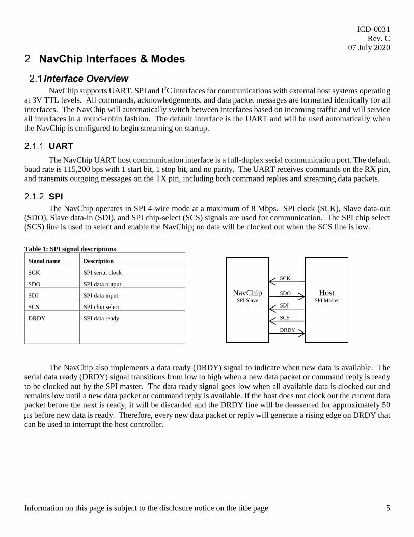
SPI
The NavChip operates in SPI 4-wire mode at a maximum of 8 Mbps. SPI clock (SCK), Slave data-out
(SDO), Slave data-in (SDI), and SPI chip-select (SCS) signals are used for communication. The SPI chip select
(SCS) line is used to select and enable the NavChip; no data will be clocked out when the SCS line is low.
Table 1: SPI signal descriptions
Signal name Description
SCK SPI serial clock
SDO SPI data output
SDI SPI data input
SCS SPI chip select
DRDY SPI data ready
The NavChip also implements a data ready (DRDY) signal to indicate when new data is available. The
serial data ready (DRDY) signal transitions from low to high when a new data packet or command reply is ready
to be clocked out by the SPI master. The data ready signal goes low when all available data is clocked out and
remains low until a new data packet or command reply is available. If the host does not clock out the current data
packet before the next is ready, it will be discarded and the DRDY line will be deasserted for approximately 50
s before new data is ready. Therefore, every new data packet or reply will generate a rising edge on DRDY that
can be used to interrupt the host controller.
NavChip SPI Slave
Host SPI Master
SCK
SDO
SDI
SCS
DRDY
ICD-0031
Rev. C
07 July 2020
Information on this page is subject to the disclosure notice on the title page 6
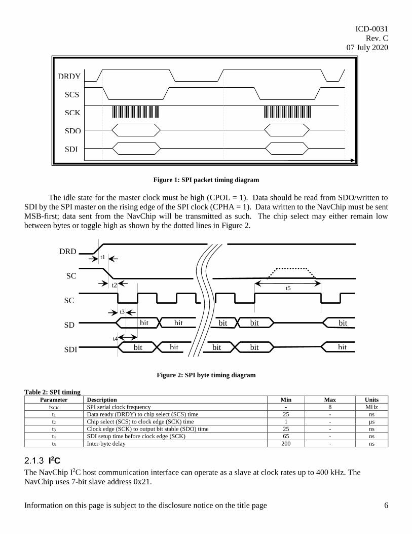
Figure 1: SPI packet timing diagram
The idle state for the master clock must be high (CPOL = 1). Data should be read from SDO/written to
SDI by the SPI master on the rising edge of the SPI clock (CPHA = 1). Data written to the NavChip must be sent
MSB-first; data sent from the NavChip will be transmitted as such. The chip select may either remain low
between bytes or toggle high as shown by the dotted lines in Figure 2.
Figure 2: SPI byte timing diagram
Table 2: SPI timing
Parameter Description Min Max Units
fSCK SPI serial clock frequency - 8 MHz
t1 Data ready (DRDY) to chip select (SCS) time 25 - ns
t2 Chip select (SCS) to clock edge (SCK) time 1 - µs
t3 Clock edge (SCK) to output bit stable (SDO) time 25 - ns
t4 SDI setup time before clock edge (SCK) 65 - ns
t5 Inter-byte delay 200 - ns
I2C
The NavChip I2C host communication interface can operate as a slave at clock rates up to 400 kHz. The
NavChip uses 7-bit slave address 0x21.
DRDY
SCS
SCK
SDO
SDI
DRD
Y
SC
S
SC
K
SD
O
SDI
t1
t3
t4
t5 t2
bit bit bit
1
bit
0
bit
7
bit bit
1
bit
0
bit
7
bit
ICD-0031
Rev. C
07 July 2020
Information on this page is subject to the disclosure notice on the title page 7
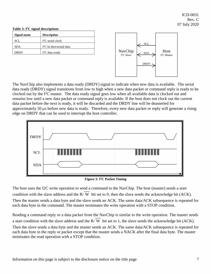
Table 3: I2C signal descriptions
Signal name Description
SCL I2C serial clock
SDA I2C bi-directional data
DRDY I2C data ready
The NavChip also implements a data ready (DRDY) signal to indicate when new data is available. The serial
data ready (DRDY) signal transitions from low to high when a new data packet or command reply is ready to be
clocked out by the I2C master. The data ready signal goes low when all available data is clocked out and
remains low until a new data packet or command reply is available. If the host does not clock out the current
data packet before the next is ready, it will be discarded and the DRDY line will be deasserted for
approximately 50 s before new data is ready. Therefore, every new data packet or reply will generate a rising
edge on DRDY that can be used to interrupt the host controller.
Figure 3: I2C Packet Timing
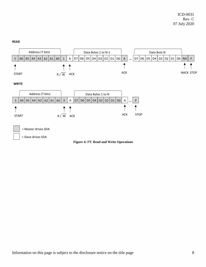
The host uses the I2C write operation to send a command to the NavChip. The host (master) sends a start
condition with the slave address and the R/ W bit set to 0, then the slave sends the acknowledge bit (ACK).
Then the master sends a data byte and the slave sends an ACK. The same data/ACK subsequence is repeated for
each data byte in the command. The master terminates the write operation with a STOP condition.
Reading a command reply or a data packet from the NavChip is similar to the write operation. The master sends
a start condition with the slave address and the R/ W bit set to 1, the slave sends the acknowledge bit (ACK).
Then the slave sends a data byte and the master sends an ACK. The same data/ACK subsequence is repeated for
each data byte in the reply or packet except that the master sends a NACK after the final data byte. The master
terminates the read operation with a STOP condition.
NavChip I2C Slave
Host I2C Master
SCL
SDA
DRDY
DRDY
SCL
SDA
ICD-0031
Rev. C
07 July 2020
Information on this page is subject to the disclosure notice on the title page 8
Figure 4: I2C Read and Write Operations
S A6 A5 A4 A3 A2 A1 A0 1
= Master drives SDA
= Slave drives SDA
READ
START R / W
Address (7 bits)
A
ACK Master
D7 D6 D5 D4 D3 D2 D1 D0 A
Data Bytes 1 to N-1
ACK Master
P
STOP
S A6 A5 A4 A3 A2 A1 A0 0
WRITE
START Master
R / W
Address (7 bits)
A
ACK Master
D7 D6 D5 D4 D3 D2 D1 D0 A
Data Bytes 1 to N
ACK Master
P
STOP
…
…
D7 D6 D5 D4 D3 D2 D1 D0 NA
Data Byte N
NACK Master
ICD-0031
Rev. C
07 July 2020
Information on this page is subject to the disclosure notice on the title page 9
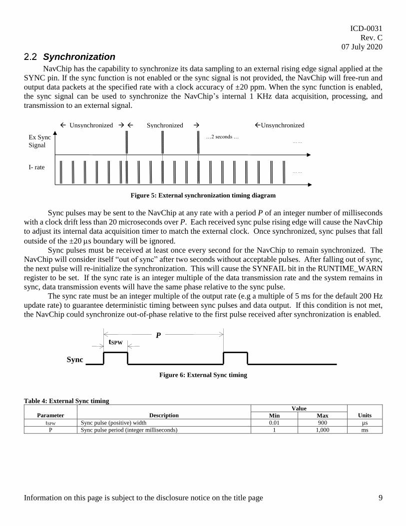
Synchronization
NavChip has the capability to synchronize its data sampling to an external rising edge signal applied at the
SYNC pin. If the sync function is not enabled or the sync signal is not provided, the NavChip will free-run and
output data packets at the specified rate with a clock accuracy of ±20 ppm. When the sync function is enabled,
the sync signal can be used to synchronize the NavChip’s internal 1 KHz data acquisition, processing, and
transmission to an external signal.
Figure 5: External synchronization timing diagram
Sync pulses may be sent to the NavChip at any rate with a period P of an integer number of milliseconds
with a clock drift less than 20 microseconds over P. Each received sync pulse rising edge will cause the NavChip
to adjust its internal data acquisition timer to match the external clock. Once synchronized, sync pulses that fall
outside of the ±20 s boundary will be ignored.
Sync pulses must be received at least once every second for the NavChip to remain synchronized. The
NavChip will consider itself “out of sync” after two seconds without acceptable pulses. After falling out of sync,
the next pulse will re-initialize the synchronization. This will cause the SYNFAIL bit in the RUNTIME_WARN
register to be set. If the sync rate is an integer multiple of the data transmission rate and the system remains in
sync, data transmission events will have the same phase relative to the sync pulse.
The sync rate must be an integer multiple of the output rate (e.g a multiple of 5 ms for the default 200 Hz
update rate) to guarantee deterministic timing between sync pulses and data output. If this condition is not met,
the NavChip could synchronize out-of-phase relative to the first pulse received after synchronization is enabled.
Figure 6: External Sync timing
Table 4: External Sync timing
Parameter
Description
Value
Units Min Max
tSPW Sync pulse (positive) width 0.01 900 µs
P Sync pulse period (integer milliseconds) 1 1,000 ms
Ex Sync
Signal
I- rate
Unsynchronized Synchronized Unsynchronized
…2 seconds …
… …
…
… …
…
tSPW
Sync
P
ICD-0031
Rev. C
07 July 2020
Information on this page is subject to the disclosure notice on the title page 10
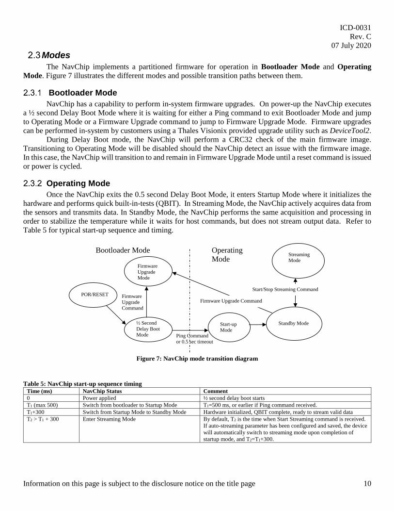
Modes
The NavChip implements a partitioned firmware for operation in Bootloader Mode and Operating
Mode. Figure 7 illustrates the different modes and possible transition paths between them.
Bootloader Mode
NavChip has a capability to perform in-system firmware upgrades. On power-up the NavChip executes
a ½ second Delay Boot Mode where it is waiting for either a Ping command to exit Bootloader Mode and jump
to Operating Mode or a Firmware Upgrade command to jump to Firmware Upgrade Mode. Firmware upgrades
can be performed in-system by customers using a Thales Visionix provided upgrade utility such as DeviceTool2.
During Delay Boot mode, the NavChip will perform a CRC32 check of the main firmware image.
Transitioning to Operating Mode will be disabled should the NavChip detect an issue with the firmware image.
In this case, the NavChip will transition to and remain in Firmware Upgrade Mode until a reset command is issued
or power is cycled.
Operating Mode
Once the NavChip exits the 0.5 second Delay Boot Mode, it enters Startup Mode where it initializes the
hardware and performs quick built-in-tests (QBIT). In Streaming Mode, the NavChip actively acquires data from
the sensors and transmits data. In Standby Mode, the NavChip performs the same acquisition and processing in
order to stabilize the temperature while it waits for host commands, but does not stream output data. Refer to
Table 5 for typical start-up sequence and timing.
Figure 7: NavChip mode transition diagram
Table 5: NavChip start-up sequence timing
Time (ms) NavChip Status Comment
0 Power applied ½ second delay boot starts
T1 (max 500) Switch from bootloader to Startup Mode T1=500 ms, or earlier if Ping command received.
T1+300 Switch from Startup Mode to Standby Mode Hardware initialized, QBIT complete, ready to stream valid data
T2 > T1 + 300
Enter Streaming Mode By default, T2 is the time when Start Streaming command is received.
If auto-streaming parameter has been configured and saved, the device
will automatically switch to streaming mode upon completion of
startup mode, and T2=T1+300.
Firmware
Upgrade Command
Firmware
Upgrade Mode
Ping Command
or 0.5 sec timeout
POR/RESET
½ Second
Delay Boot Mode
Streaming Mode
Standby Mode
Firmware Upgrade Command
Bootloader Mode
Operating
Mode
Start-up Mode
Start/Stop Streaming Command
ICD-0031
Rev. C
07 July 2020
Information on this page is subject to the disclosure notice on the title page 11
Communications protocol
Command Structure
Commands begin with a start byte and a header byte formatted as shown in Table 6. Some commands
include a body, typically containing additional command parameters and data. A Two’s Complement checksum
of all preceding bytes is added to the end of the command. Little-endian format is used for multi-byte words for
communication and addressing within the NavChip. All signed integers use the two’s complement format.
The start byte is always 0xA5. The header byte consists of an address nibble and a command nibble.
Address specifies the recipient device; in the future a feature may be added to allow up to 8 unique devices to
communicate on a single communication port. Until then, there is no reason to change the address from its default
value of zero.
Table 6: Command packet structure
Bit 7 Bit 6 Bit 5 Bit 4 Bit 3 Bit 2 Bit 1 Bit 0
0xA 0x5
Spare Address (0-7) Command (0-15)
Body (command-dependent)
Checksum
The commands supported by the NavChip are listed in section 3.4.
Reply Structure
Replies start with an echo of the command header byte and may be followed by additional data bytes
depending on the command. Replies that include a body (typically containing data) also have a checksum
appended, which includes all preceding bytes.
Table 7: Reply packet structure
Bit 7 Bit 6 Bit 5 Bit 4 Bit 3 Bit 2 Bit 1 Bit 0
Command header echo
Reply data byte(s)*
Checksum*
Note: *Present only when reply includes a body.
ICD-0031
Rev. C
07 July 2020
Information on this page is subject to the disclosure notice on the title page 12
Data and baud rates
The NavChip always updates internally at exactly 1000 Hz (+/- 0.05 Hz) but is capable of transmitting
data at any rate listed in Table 8.
Table 8: NavChip data output rate
data rate = data rate max/divisor
data rate divisor output data rate
1 1000.000 Hz
2 500.000 Hz
3 333.333 Hz
4 250.000 Hz
5 200.000 Hz (default)
6 166.667 Hz
7 142.857 Hz
8 125.000 Hz
9 111.111 Hz
10 100.000 Hz
Communication can occur at a maximum baud rate of 921,600 or any other rate listed in Table 9. Other
divisors will not be rejected (and will set the baud rate to the expected rate), but only the divisors listed in Table
9 are officially supported (they are guaranteed to have under 1% error from the actual rate).
Table 9: NavChip baud rates
baud rate = baud rate max/divisor
baud rate divisor output baud rate
1 921,600
2 460,800
4 230,400
8 115,200 (default)
24 38,400
Beware when programming the communications parameters that the baud rate must be high enough to
support the chosen data rate and packet type combination. For a packet type with total length N bytes, the length
will be 10*N bits (including the start and stop bit), so the baud rate should be at least 20% higher than 10*N*data
rate. If not, the NavChip will drop data packets whenever the serial port transmission cannot keep up with the
rate at which new data is being generated. Higher data rates will cause the NavChip to draw more current (consult
the datasheet for details).
ICD-0031
Rev. C
07 July 2020
Information on this page is subject to the disclosure notice on the title page 13
Command Set
Please refer to the key below for notation frequently used in the command syntax.
Key:
<s> Start byte s=0xA5
<ax> Header byte where a=device address, x=command
<d> Data byte
<ct> Total number of bytes in a command, including header and checksum
<cs> Checksum byte (negative sum of all preceding bytes)
<ma> Represents a register address
For example, the command to obtain the results of register 0 would be the four hex-format bytes A5 01
00 5A (the get register format is <s><a1><ma><cs>).
Note that a small number of simple commands are used to interface with and control the NavChip, and
that all configuration is performed by setting registers. Configuration and status information can be obtained by
reading registers directly, or via information streamed out along with the data itself in data packets.
Streaming status includes the presence or absence of a fault condition, the magnetometer axis being
reported (for devices with magnetometers), and an “S” bit in the discrete status byte (see Table 11) that may be
used to construct registers 0-31 after a complete frame (256 records). These registers include a temperature
register, runtime warning flags and synchronization status.
All commands – with the exception of Diagnostics, Set Register (<ma> = 0xFF), and Set NVRAM (<ma>
= 0xFFFF) – will execute within 5 milliseconds. Invalid commands or commands with invalid parameters are
not executed or acknowledged.
ICD-0031
Rev. C
07 July 2020
Information on this page is subject to the disclosure notice on the title page 14
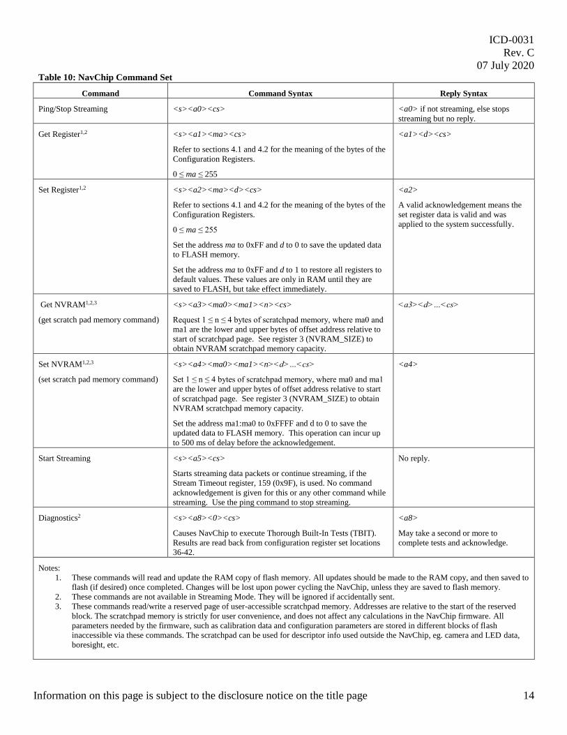
Table 10: NavChip Command Set
Command Command Syntax Reply Syntax
Ping/Stop Streaming <s><a0><cs> <a0> if not streaming, else stops
streaming but no reply.
Get Register1,2
<s><a1><ma><cs>
Refer to sections 4.1 and 4.2 for the meaning of the bytes of the
Configuration Registers.
0 ≤ ma ≤ 255
<a1><d><cs>
Set Register1,2
<s><a2><ma><d><cs>
Refer to sections 4.1 and 4.2 for the meaning of the bytes of the
Configuration Registers.
0 ≤ ma ≤ 255
Set the address ma to 0xFF and d to 0 to save the updated data
to FLASH memory.
Set the address ma to 0xFF and d to 1 to restore all registers to
default values. These values are only in RAM until they are
saved to FLASH, but take effect immediately.
<a2>
A valid acknowledgement means the
set register data is valid and was
applied to the system successfully.
Get NVRAM1,2,3
(get scratch pad memory command)
<s><a3><ma0><ma1><n><cs>
Request 1 ≤ n ≤ 4 bytes of scratchpad memory, where ma0 and
ma1 are the lower and upper bytes of offset address relative to
start of scratchpad page. See register 3 (NVRAM_SIZE) to
obtain NVRAM scratchpad memory capacity.
<a3><d>…<cs>
Set NVRAM1,2,3
(set scratch pad memory command)
<s><a4><ma0><ma1><n><d>…<cs>
Set 1 ≤ n ≤ 4 bytes of scratchpad memory, where ma0 and ma1
are the lower and upper bytes of offset address relative to start
of scratchpad page. See register 3 (NVRAM_SIZE) to obtain
NVRAM scratchpad memory capacity.
Set the address ma1:ma0 to 0xFFFF and d to 0 to save the
updated data to FLASH memory. This operation can incur up
to 500 ms of delay before the acknowledgement.
<a4>
Start Streaming <s><a5><cs>
Starts streaming data packets or continue streaming, if the
Stream Timeout register, 159 (0x9F), is used. No command
acknowledgement is given for this or any other command while
streaming. Use the ping command to stop streaming.
No reply.
Diagnostics2
<s><a8><0><cs>
Causes NavChip to execute Thorough Built-In Tests (TBIT).
Results are read back from configuration register set locations
36-42.
<a8>
May take a second or more to
complete tests and acknowledge.
Notes:
1. These commands will read and update the RAM copy of flash memory. All updates should be made to the RAM copy, and then saved to
flash (if desired) once completed. Changes will be lost upon power cycling the NavChip, unless they are saved to flash memory.
2. These commands are not available in Streaming Mode. They will be ignored if accidentally sent.
3. These commands read/write a reserved page of user-accessible scratchpad memory. Addresses are relative to the start of the reserved
block. The scratchpad memory is strictly for user convenience, and does not affect any calculations in the NavChip firmware. All
parameters needed by the firmware, such as calibration data and configuration parameters are stored in different blocks of flash
inaccessible via these commands. The scratchpad can be used for descriptor info used outside the NavChip, eg. camera and LED data,
boresight, etc.
ICD-0031
Rev. C
07 July 2020
Information on this page is subject to the disclosure notice on the title page 15
Error & Status Reporting (QBIT/TBIT/CBIT)
The NavChip has several mechanisms for reporting errors: QBIT (Quick Built-In Test), CBIT (Continuous
Built-In Test) and TBIT (Thorough Built-In Test). Once performed, tests provide results by updating
Configuration Registers 36-42 to provide details of the problem.
CBIT results persist until the end of the frame in which they appear (up to 256 packets, depending on the
packet ID when they first appear). The specific packet which contains the CBIT error is indicated by the fault
(`F`) flag in the packet’s discrete flag byte (if enabled). CBIT results are cleared at the start of each frame. These
tests update registers 23, 38, 39, and 42.
TBIT – initiated with the Diagnostic command – performs a detailed test of all internal inertial sensors.
TBIT is able to detect serious issues with the internal sensors, such as mechanical or electrical failures, though it
does require the sensor to be stationary in order to accurately report failures. If failures are indicated, please
provide a brief logged data file (which includes all registers) to allow Technical Support to assist in
troubleshooting the issue. These tests update registers 36 and 37.
QBIT is always executed once upon initialization and only checks for basic issues that can arise during
system initialization. These tests update registers 36, 37, 40, and 41.
Data Packet Items
PacketID
PacketID is an 8-bit sequence counter of the packet number relative to the start of this 256-record data
frame. This can be used to decode the Configuration Registers one bit or one byte at a time during streaming
mode (see the S flag description in Table 11).
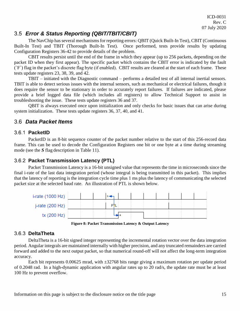
Packet Transmission Latency (PTL)
Packet Transmission Latency is a 16-bit unsigned value that represents the time in microseconds since the
final i-rate of the last data integration period (whose integral is being transmitted in this packet). This implies
that the latency of reporting is the integration cycle time plus 1 ms plus the latency of communicating the selected
packet size at the selected baud rate. An illustration of PTL is shown below.
Figure 8: Packet Transmission Latency & Output Latency
DeltaTheta
DeltaTheta is a 16-bit signed integer representing the incremental rotation vector over the data integration
period. Angular integrals are maintained internally with higher precision, and any truncated remainders are carried
forward and added to the next output packet, so that numerical round-off will not affect the long-term integration
accuracy.
Each bit represents 0.00625 mrad, with ±32768 bits range giving a maximum rotation per update period
of 0.2048 rad. In a high-dynamic application with angular rates up to 20 rad/s, the update rate must be at least
100 Hz to prevent overflow.
ICD-0031
Rev. C
07 July 2020
Information on this page is subject to the disclosure notice on the title page 16
DeltaV
DeltaV is a 16-bit signed integer representing the integral of accelerometer measurements over the data
integration period. Velocity integrals are maintained internally with higher precision, and any truncated
remainders are carried forward and added to the next output packet, so that numerical round-off will not affect
the long-term integration accuracy.
Each bit represents 39.0625e-6 m/s, with ±32768 bits range, giving a maximum velocity change per
update period of 1.28 m/s. In a high dynamic application with linear accelerations up to the maximum 120
m/s/s that the NavChip can measure, the update rate must be at least 100 Hz to prevent overflow.
Temperature
Temperature is the current temperature of the NavChip, typically several degrees warmer than the ambient
air. The value is a 16-bit signed integer, and each bit represents 0.05 °C. This is the same value reported by the
ENVIRO_2 and ENVIRO_1 registers (27 and 26), but can be streamed continuously in packet type 20 (see section
3.8.3) to allow continuous monitoring of the sensor temperature without stopping data streaming. Note that while
this is reported as a 12-bit value in the registers, it is reported as a 16-bit value as an output item. The resolution
is the same in both cases.
Vin
Vin is a 16-bit unsigned integer representing the NavChip’s input voltage (reported up to a maximum of
6V). Resolution of this field is 2.336e-3 V/LSB. This is the same value reported by the ENVIRO_1 and
ENVIRO_0 registers (26 and 25), but can be streamed continuously in packet type 20 (see section 3.8.3) to allow
continuous monitoring of the sensor voltage without stopping data streaming. Note that while this is reported as
a 12-bit value in the registers, it is reported as a 16-bit value as an output item; the resolution is the same in both.
ICD-0031
Rev. C
07 July 2020
Information on this page is subject to the disclosure notice on the title page 17
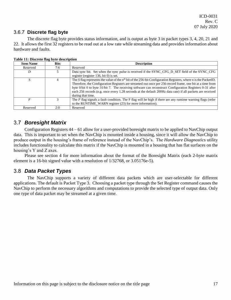
Discrete flag byte
The discrete flag byte provides status information, and is output as byte 3 in packet types 3, 4, 20, 21 and
22. It allows the first 32 registers to be read out at a low rate while streaming data and provides information about
hardware and faults.
Table 11: Discrete flag byte description
Item Name Bits Description
Reserved 7:6 Reserved
D 5 Data sync bit. Set when the sync pulse is received if the SYNC_CFG_D_SET field of the SYNC_CFG
register (register 136, bit 0) is set.
S 4 The S flag represents the value of the nth bit of the 256-bit Configuration Registers, where n is the PacketID.
Therefore, the Configuration Registers are streamed out once per 256-record frame, one bit at a time from
byte 0/bit 0 to byte 31/bit 7. The receiving software can reconstruct Configuration Registers 0-31 after
each 256 records (e.g. once every 1.28 seconds at the default 200Hz data rate) if all packets are received
during that time.
F 3 The F flag signals a fault condition. The F flag will be high if there are any runtime warning flags (refer
to the RUNTIME_WARN register (23) for more information).
Reserved 2:0 Reserved
Boresight Matrix
Configuration Registers 44 – 61 allow for a user-provided boresight matrix to be applied to NavChip output
data. This is important to set when the NavChip is mounted inside a housing, since it will allow the NavChip to
produce output in the housing’s frame of reference instead of the NavChip’s. The Hardware Diagnostics utility
includes functionality to calculate this matrix if the NavChip is mounted in a housing that has flat surfaces on the
housing’s Y and Z axes.
Please see section 4 for more information about the format of the Boresight Matrix (each 2-byte matrix
element is a 16-bit signed value with a resolution of 1/32768, or 3.05176e-5).
Data Packet Types
The NavChip supports a variety of different data packets which are user-selectable for different
applications. The default is Packet Type 3. Choosing a packet type through the Set Register command causes the
NavChip to perform the necessary algorithms and computations to provide the selected type of output data. Only
one type of data packet may be streamed at a given time.
ICD-0031
Rev. C
07 July 2020
Information on this page is subject to the disclosure notice on the title page 18
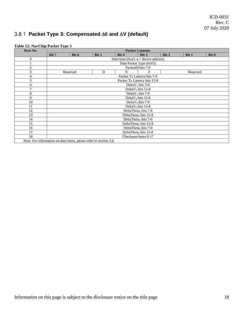
Packet Type 3: Compensated and V (default)
Table 12: NavChip Packet Type 3
Byte No. Packet Contents
Bit 7 Bit 6 Bit 5 Bit 4 Bit 3 Bit 2 Bit 1 Bit 0
0 Start byte (0xa5, a = device address)
1 Data Packet Type (0x03)
2 PacketID bits 7-0
3 Reserved D S F Reserved
4 Packet Tx Latency bits 7-0
5 Packet Tx Latency bits 15-8
6 DeltaVx bits 7-0
7 DeltaVx bits 15-8
8 DeltaVy bits 7-0
9 DeltaVy bits 15-8
10 DeltaVz bits 7-0
11 DeltaVz bits 15-8
12 DeltaThetax bits 7-0
13 DeltaThetax bits 15-8
14 DeltaThetay bits 7-0
15 DeltaThetay bits 15-8
16 DeltaThetaz bits 7-0
17 DeltaThetaz bits 15-8
18 Checksum bytes 0-17
Note: For information on data items, please refer to section 3.6.
ICD-0031
Rev. C
07 July 2020
Information on this page is subject to the disclosure notice on the title page 19
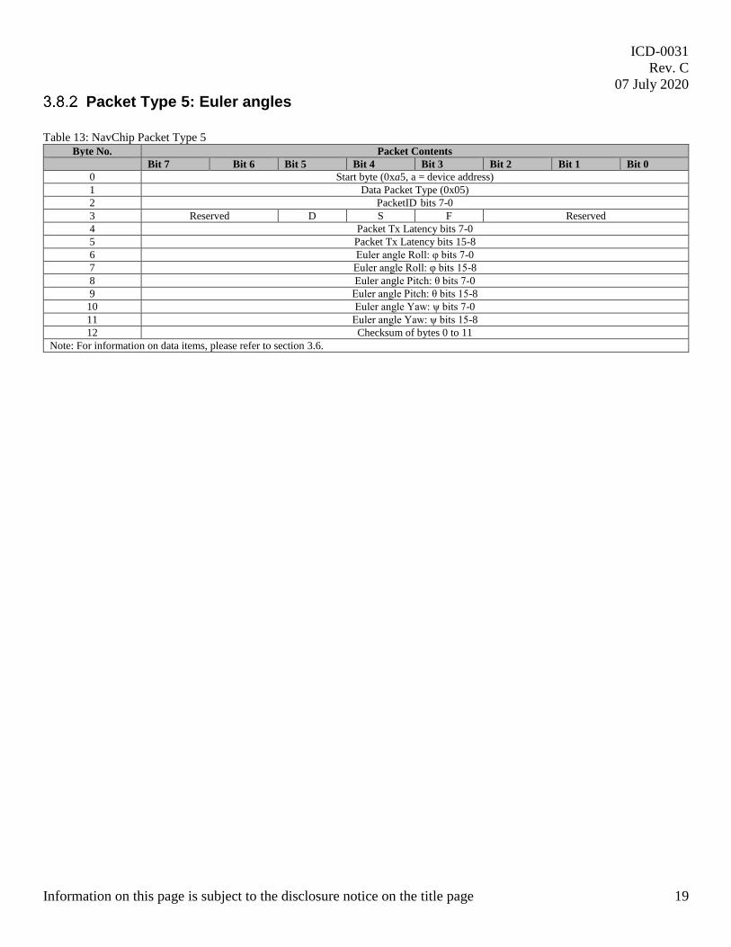
Packet Type 5: Euler angles
Table 13: NavChip Packet Type 5
Byte No. Packet Contents
Bit 7 Bit 6 Bit 5 Bit 4 Bit 3 Bit 2 Bit 1 Bit 0
0 Start byte (0xa5, a = device address)
1 Data Packet Type (0x05)
2 PacketID bits 7-0
3 Reserved D S F Reserved
4 Packet Tx Latency bits 7-0
5 Packet Tx Latency bits 15-8
6 Euler angle Roll: φ bits 7-0
7 Euler angle Roll: φ bits 15-8
8 Euler angle Pitch: θ bits 7-0
9 Euler angle Pitch: θ bits 15-8
10 Euler angle Yaw: ψ bits 7-0
11 Euler angle Yaw: ψ bits 15-8
12 Checksum of bytes 0 to 11
Note: For information on data items, please refer to section 3.6.
ICD-0031
Rev. C
07 July 2020
Information on this page is subject to the disclosure notice on the title page 20
Configuration Register Set (CRS) The Configuration Register Set is a 256-byte block of memory containing all of the NavChip’s current
operating state information, including constants, user-configured parameters, and built-in self-test results. There
are multiple ways to read information out of the Configuration Registers:
1) Get Register command reads out any byte(s) in any order.
2) In Streaming Mode, packet types 3, 4, 20, 21 and 22 contain an “S”-bit which cycles through the first
256 bits (32 bytes) of the Configuration Register Set, allowing the receiving program to reconstruct the
most important status information once per 256-packet frame.
ICD-0031
Rev. C
07 July 2020
Information on this page is subject to the disclosure notice on the title page 21
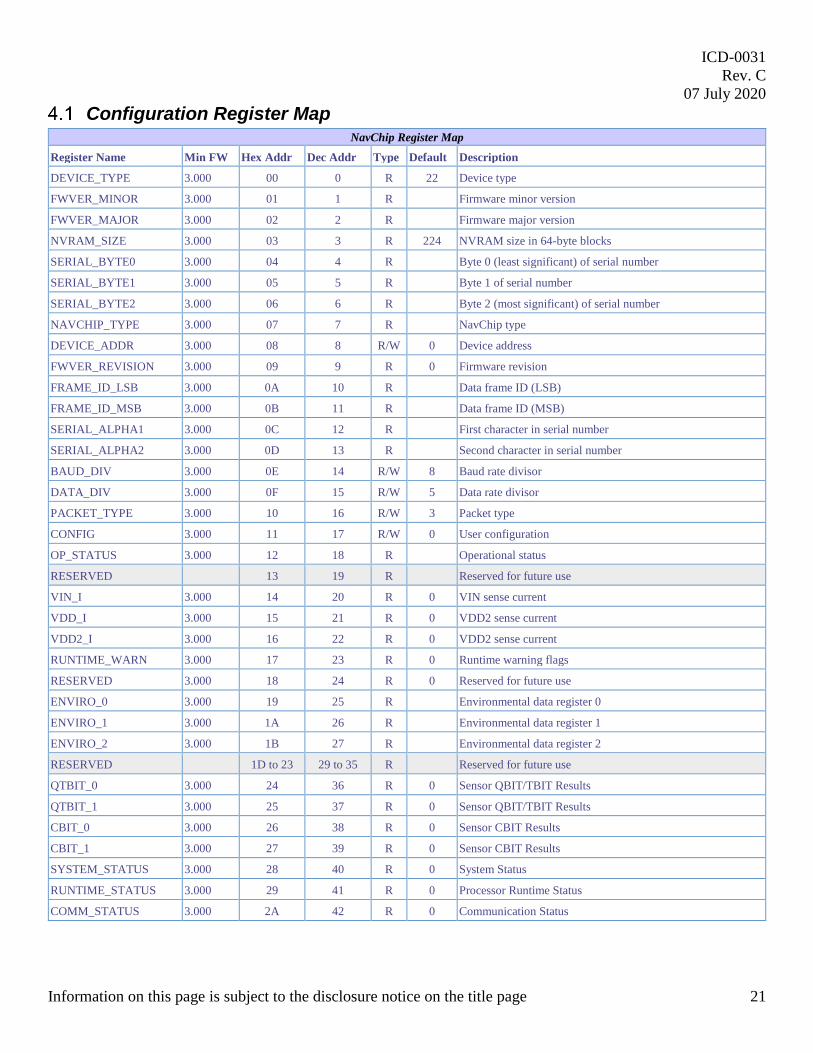
Configuration Register Map NavChip Register Map
Register Name Min FW Hex Addr Dec Addr Type Default Description
DEVICE_TYPE 3.000 00 0 R 22 Device type
FWVER_MINOR 3.000 01 1 R
Firmware minor version
FWVER_MAJOR 3.000 02 2 R
Firmware major version
NVRAM_SIZE 3.000 03 3 R 224 NVRAM size in 64-byte blocks
SERIAL_BYTE0 3.000 04 4 R
Byte 0 (least significant) of serial number
SERIAL_BYTE1 3.000 05 5 R
Byte 1 of serial number
SERIAL_BYTE2 3.000 06 6 R
Byte 2 (most significant) of serial number
NAVCHIP_TYPE 3.000 07 7 R
NavChip type
DEVICE_ADDR 3.000 08 8 R/W 0 Device address
FWVER_REVISION 3.000 09 9 R 0 Firmware revision
FRAME_ID_LSB 3.000 0A 10 R
Data frame ID (LSB)
FRAME_ID_MSB 3.000 0B 11 R
Data frame ID (MSB)
SERIAL_ALPHA1 3.000 0C 12 R
First character in serial number
SERIAL_ALPHA2 3.000 0D 13 R
Second character in serial number
BAUD_DIV 3.000 0E 14 R/W 8 Baud rate divisor
DATA_DIV 3.000 0F 15 R/W 5 Data rate divisor
PACKET_TYPE 3.000 10 16 R/W 3 Packet type
CONFIG 3.000 11 17 R/W 0 User configuration
OP_STATUS 3.000 12 18 R
Operational status
RESERVED
13 19 R
Reserved for future use
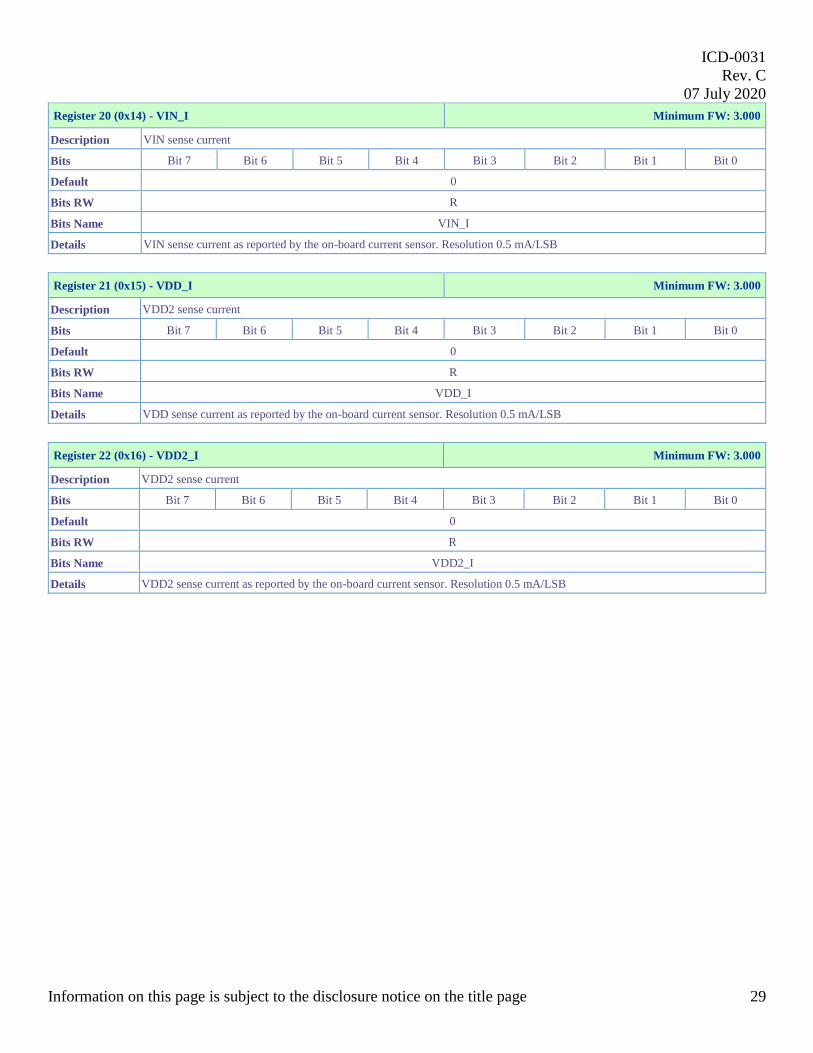
VIN_I 3.000 14 20 R 0 VIN sense current
VDD_I 3.000 15 21 R 0 VDD2 sense current
VDD2_I 3.000 16 22 R 0 VDD2 sense current
RUNTIME_WARN 3.000 17 23 R 0 Runtime warning flags
RESERVED 3.000 18 24 R 0 Reserved for future use
ENVIRO_0 3.000 19 25 R
Environmental data register 0
ENVIRO_1 3.000 1A 26 R
Environmental data register 1
ENVIRO_2 3.000 1B 27 R
Environmental data register 2
RESERVED
1D to 23 29 to 35 R
Reserved for future use
QTBIT_0 3.000 24 36 R 0 Sensor QBIT/TBIT Results
QTBIT_1 3.000 25 37 R 0 Sensor QBIT/TBIT Results
CBIT_0 3.000 26 38 R 0 Sensor CBIT Results
CBIT_1 3.000 27 39 R 0 Sensor CBIT Results
SYSTEM_STATUS 3.000 28 40 R 0 System Status
RUNTIME_STATUS 3.000 29 41 R 0 Processor Runtime Status
COMM_STATUS 3.000 2A 42 R 0 Communication Status
ICD-0031
Rev. C
07 July 2020
Information on this page is subject to the disclosure notice on the title page 22
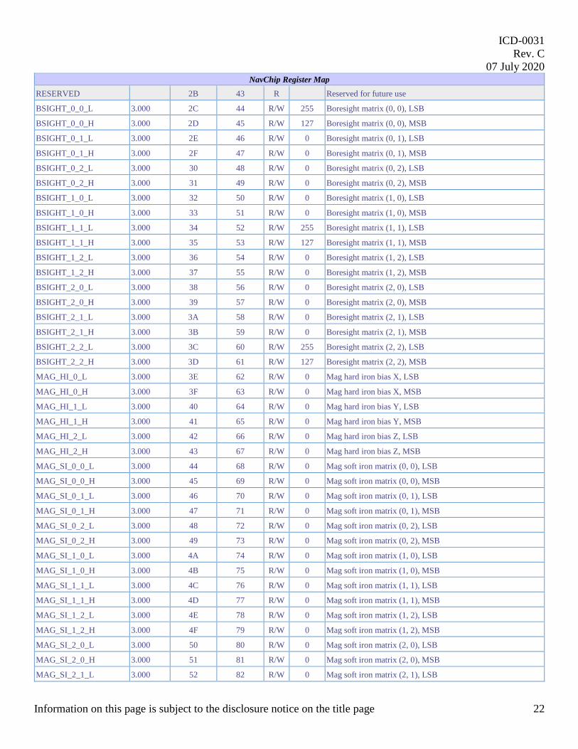
NavChip Register Map
RESERVED
2B 43 R
Reserved for future use
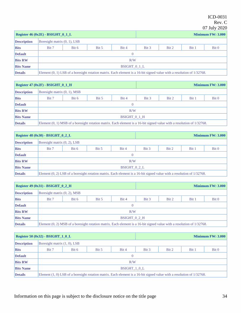
BSIGHT_0_0_L 3.000 2C 44 R/W 255 Boresight matrix (0, 0), LSB
BSIGHT_0_0_H 3.000 2D 45 R/W 127 Boresight matrix (0, 0), MSB
BSIGHT_0_1_L 3.000 2E 46 R/W 0 Boresight matrix (0, 1), LSB
BSIGHT_0_1_H 3.000 2F 47 R/W 0 Boresight matrix (0, 1), MSB
BSIGHT_0_2_L 3.000 30 48 R/W 0 Boresight matrix (0, 2), LSB
BSIGHT_0_2_H 3.000 31 49 R/W 0 Boresight matrix (0, 2), MSB
BSIGHT_1_0_L 3.000 32 50 R/W 0 Boresight matrix (1, 0), LSB
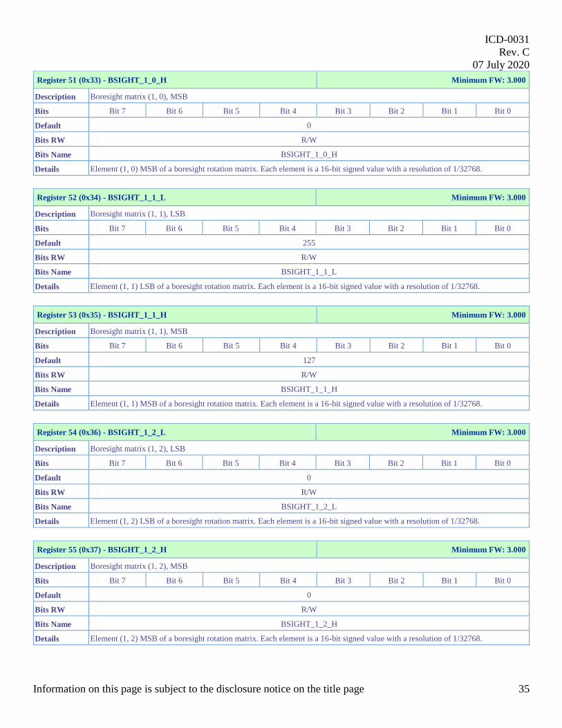
BSIGHT_1_0_H 3.000 33 51 R/W 0 Boresight matrix (1, 0), MSB
BSIGHT_1_1_L 3.000 34 52 R/W 255 Boresight matrix (1, 1), LSB
BSIGHT_1_1_H 3.000 35 53 R/W 127 Boresight matrix (1, 1), MSB
BSIGHT_1_2_L 3.000 36 54 R/W 0 Boresight matrix (1, 2), LSB
BSIGHT_1_2_H 3.000 37 55 R/W 0 Boresight matrix (1, 2), MSB
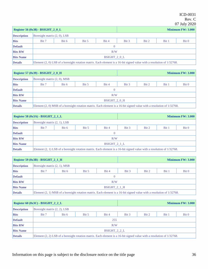
BSIGHT_2_0_L 3.000 38 56 R/W 0 Boresight matrix (2, 0), LSB
BSIGHT_2_0_H 3.000 39 57 R/W 0 Boresight matrix (2, 0), MSB
BSIGHT_2_1_L 3.000 3A 58 R/W 0 Boresight matrix (2, 1), LSB
BSIGHT_2_1_H 3.000 3B 59 R/W 0 Boresight matrix (2, 1), MSB
BSIGHT_2_2_L 3.000 3C 60 R/W 255 Boresight matrix (2, 2), LSB
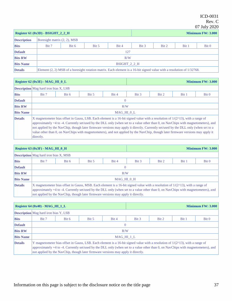
BSIGHT_2_2_H 3.000 3D 61 R/W 127 Boresight matrix (2, 2), MSB
MAG_HI_0_L 3.000 3E 62 R/W 0 Mag hard iron bias X, LSB
MAG_HI_0_H 3.000 3F 63 R/W 0 Mag hard iron bias X, MSB
MAG_HI_1_L 3.000 40 64 R/W 0 Mag hard iron bias Y, LSB
MAG_HI_1_H 3.000 41 65 R/W 0 Mag hard iron bias Y, MSB
MAG_HI_2_L 3.000 42 66 R/W 0 Mag hard iron bias Z, LSB
MAG_HI_2_H 3.000 43 67 R/W 0 Mag hard iron bias Z, MSB
MAG_SI_0_0_L 3.000 44 68 R/W 0 Mag soft iron matrix (0, 0), LSB
MAG_SI_0_0_H 3.000 45 69 R/W 0 Mag soft iron matrix (0, 0), MSB
MAG_SI_0_1_L 3.000 46 70 R/W 0 Mag soft iron matrix (0, 1), LSB
MAG_SI_0_1_H 3.000 47 71 R/W 0 Mag soft iron matrix (0, 1), MSB
MAG_SI_0_2_L 3.000 48 72 R/W 0 Mag soft iron matrix (0, 2), LSB
MAG_SI_0_2_H 3.000 49 73 R/W 0 Mag soft iron matrix (0, 2), MSB
MAG_SI_1_0_L 3.000 4A 74 R/W 0 Mag soft iron matrix (1, 0), LSB
MAG_SI_1_0_H 3.000 4B 75 R/W 0 Mag soft iron matrix (1, 0), MSB
MAG_SI_1_1_L 3.000 4C 76 R/W 0 Mag soft iron matrix (1, 1), LSB
MAG_SI_1_1_H 3.000 4D 77 R/W 0 Mag soft iron matrix (1, 1), MSB
MAG_SI_1_2_L 3.000 4E 78 R/W 0 Mag soft iron matrix (1, 2), LSB
MAG_SI_1_2_H 3.000 4F 79 R/W 0 Mag soft iron matrix (1, 2), MSB
MAG_SI_2_0_L 3.000 50 80 R/W 0 Mag soft iron matrix (2, 0), LSB
MAG_SI_2_0_H 3.000 51 81 R/W 0 Mag soft iron matrix (2, 0), MSB
MAG_SI_2_1_L 3.000 52 82 R/W 0 Mag soft iron matrix (2, 1), LSB
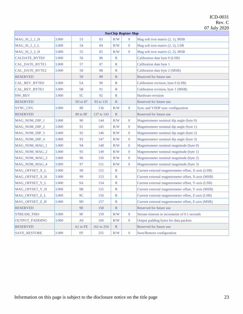
ICD-0031
Rev. C
07 July 2020
Information on this page is subject to the disclosure notice on the title page 23
NavChip Register Map
MAG_SI_2_1_H 3.000 53 83 R/W 0 Mag soft iron matrix (2, 1), MSB
MAG_SI_2_2_L 3.000 54 84 R/W 0 Mag soft iron matrix (2, 2), LSB
MAG_SI_2_2_H 3.000 55 85 R/W 0 Mag soft iron matrix (2, 2), MSB
CALDATE_BYTE0 3.000 56 86 R
Calibration date byte 0 (LSB)
CAL_DATE_BYTE1 3.000 57 87 R
Calibration date byte 1
CAL_DATE_BYTE2 3.000 58 88 R
Calibration date byte 2 (MSB)
RESERVED
59 89 R
Reserved for future use
CAL_REV_BYTE0 3.000 5A 90 R
Calibration revision, byte 0 (LSB)
CAL_REV_BYTE1 3.000 5B 91 R
Calibration revision, byte 1 (MSB)
HW_REV 3.000 5C 92 R
Hardware revision
RESERVED
5D to 87 93 to 135 R
Reserved for future use
SYNC_CFG 3.000 88 136 R/W 0 Sync and VSDP sync configuration
RESERVED
89 to 8F 137 to 143 R
Reserved for future use
MAG_NOM_DIP_1 3.000 90 144 R/W 0 Magnetometer nominal dip angle (byte 0)
MAG_NOM_DIP_2 3.000 91 145 R/W 0 Magnetometer nominal dip angle (byte 1)
MAG_NOM_DIP_3 3.000 92 146 R/W 0 Magnetometer nominal dip angle (byte 2)
MAG_NOM_DIP_4 3.000 93 147 R/W 0 Magnetometer nominal dip angle (byte 3)
MAG_NOM_MAG_1 3.000 94 148 R/W 0 Magnetometer nominal magnitude (byte 0)
MAG_NOM_MAG_2 3.000 95 149 R/W 0 Magnetometer nominal magnitude (byte 1)
MAG_NOM_MAG_3 3.000 96 150 R/W 0 Magnetometer nominal magnitude (byte 2)
MAG_NOM_MAG_4 3.000 97 151 R/W 0 Magnetometer nominal magnitude (byte 3)
MAG_OFFSET_X_L 3.000 98 152 R
Current external magnetometer offset, X-axis (LSB)
MAG_OFFSET_X_H 3.000 99 153 R
Current external magnetometer offset, X-axis (MSB)
MAG_OFFSET_Y_L 3.000 9A 154 R
Current external magnetometer offset, Y-axis (LSB)
MAG_OFFSET_Y_H 3.000 9B 155 R
Current external magnetometer offset, Y-axis (MSB)
MAG_OFFSET_Z_L 3.000 9C 156 R
Current external magnetometer offset, Z-axis (LSB)
MAG_OFFSET_Z_H 3.000 9D 157 R
Current external magnetometer offset, Z-axis (MSB)
RESERVED
9E 158 R
Reserved for future use
STREAM_TMO 3.000 9F 159 R/W 0 Stream timeout in increments of 0.1 seconds
OUTPUT_PADDING 3.000 A0 160 R/W 0 Output padding bytes for data packets
RESERVED
A1 to FE 161 to 254 R
Reserved for future use
SAVE_RESTORE 3.000 FF 255 R/W 0 Save/Restore configuration
ICD-0031
Rev. C
07 July 2020
Information on this page is subject to the disclosure notice on the title page 24
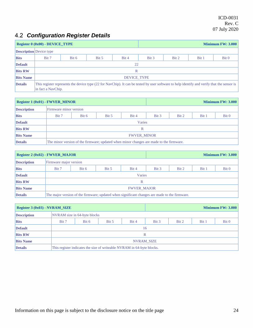
Configuration Register Details
Register 0 (0x00) - DEVICE_TYPE Minimum FW: 3.000
Description Device type
Bits Bit 7 Bit 6 Bit 5 Bit 4 Bit 3 Bit 2 Bit 1 Bit 0
Default 22
Bits RW R
Bits Name DEVICE_TYPE
Details This register represents the device type (22 for NavChip). It can be tested by user software to help identify and verify that the sensor is
in fact a NavChip.
Register 1 (0x01) - FWVER_MINOR Minimum FW: 3.000
Description Firmware minor version
Bits Bit 7 Bit 6 Bit 5 Bit 4 Bit 3 Bit 2 Bit 1 Bit 0
Default Varies
Bits RW R
Bits Name FWVER_MINOR
Details The minor version of the firmware; updated when minor changes are made to the firmware.
Register 2 (0x02) - FWVER_MAJOR Minimum FW: 3.000
Description Firmware major version
Bits Bit 7 Bit 6 Bit 5 Bit 4 Bit 3 Bit 2 Bit 1 Bit 0
Default Varies
Bits RW R
Bits Name FWVER_MAJOR
Details The major version of the firmware; updated when significant changes are made to the firmware.
Register 3 (0x03) - NVRAM_SIZE Minimum FW: 3.000
Description NVRAM size in 64-byte blocks
Bits Bit 7 Bit 6 Bit 5 Bit 4 Bit 3 Bit 2 Bit 1 Bit 0
Default 16
Bits RW R
Bits Name NVRAM_SIZE
Details This register indicates the size of writeable NVRAM in 64-byte blocks.
ICD-0031
Rev. C
07 July 2020
Information on this page is subject to the disclosure notice on the title page 25
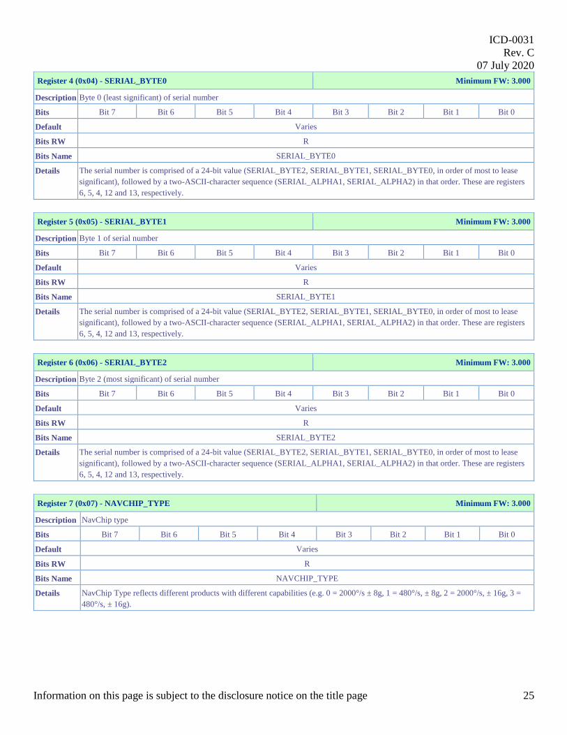
Register 4 (0x04) - SERIAL_BYTE0 Minimum FW: 3.000
Description Byte 0 (least significant) of serial number
Bits Bit 7 Bit 6 Bit 5 Bit 4 Bit 3 Bit 2 Bit 1 Bit 0
Default Varies
Bits RW R
Bits Name SERIAL_BYTE0
Details The serial number is comprised of a 24-bit value (SERIAL_BYTE2, SERIAL_BYTE1, SERIAL_BYTE0, in order of most to lease
significant), followed by a two-ASCII-character sequence (SERIAL_ALPHA1, SERIAL_ALPHA2) in that order. These are registers
6, 5, 4, 12 and 13, respectively.
Register 5 (0x05) - SERIAL_BYTE1 Minimum FW: 3.000
Description Byte 1 of serial number
Bits Bit 7 Bit 6 Bit 5 Bit 4 Bit 3 Bit 2 Bit 1 Bit 0
Default Varies
Bits RW R
Bits Name SERIAL_BYTE1
Details The serial number is comprised of a 24-bit value (SERIAL_BYTE2, SERIAL_BYTE1, SERIAL_BYTE0, in order of most to lease
significant), followed by a two-ASCII-character sequence (SERIAL_ALPHA1, SERIAL_ALPHA2) in that order. These are registers
6, 5, 4, 12 and 13, respectively.
Register 6 (0x06) - SERIAL_BYTE2 Minimum FW: 3.000
Description Byte 2 (most significant) of serial number
Bits Bit 7 Bit 6 Bit 5 Bit 4 Bit 3 Bit 2 Bit 1 Bit 0
Default Varies
Bits RW R
Bits Name SERIAL_BYTE2
Details The serial number is comprised of a 24-bit value (SERIAL_BYTE2, SERIAL_BYTE1, SERIAL_BYTE0, in order of most to lease
significant), followed by a two-ASCII-character sequence (SERIAL_ALPHA1, SERIAL_ALPHA2) in that order. These are registers
6, 5, 4, 12 and 13, respectively.
Register 7 (0x07) - NAVCHIP_TYPE Minimum FW: 3.000
Description NavChip type
Bits Bit 7 Bit 6 Bit 5 Bit 4 Bit 3 Bit 2 Bit 1 Bit 0
Default Varies
Bits RW R
Bits Name NAVCHIP_TYPE
Details NavChip Type reflects different products with different capabilities (e.g. 0 = 2000°/s ± 8g, 1 = 480°/s, ± 8g, 2 = 2000°/s, ± 16g, 3 =
480°/s, ± 16g).
ICD-0031
Rev. C
07 July 2020
Information on this page is subject to the disclosure notice on the title page 26
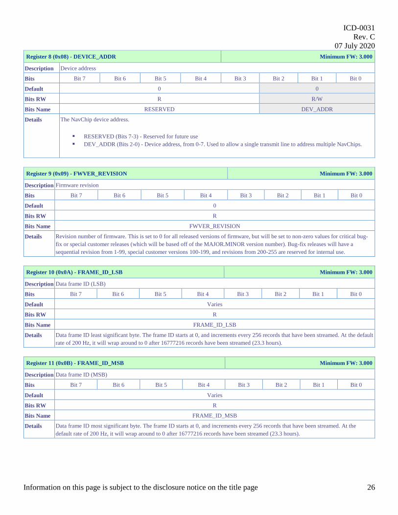
Register 8 (0x08) - DEVICE_ADDR Minimum FW: 3.000
Description Device address
Bits Bit 7 Bit 6 Bit 5 Bit 4 Bit 3 Bit 2 Bit 1 Bit 0
Default 0 0
Bits RW R R/W
Bits Name RESERVED DEV_ADDR
Details The NavChip device address.
RESERVED (Bits 7-3) - Reserved for future use
DEV_ADDR (Bits 2-0) - Device address, from 0-7. Used to allow a single transmit line to address multiple NavChips.
Register 9 (0x09) - FWVER_REVISION Minimum FW: 3.000
Description Firmware revision
Bits Bit 7 Bit 6 Bit 5 Bit 4 Bit 3 Bit 2 Bit 1 Bit 0
Default 0
Bits RW R
Bits Name FWVER_REVISION
Details Revision number of firmware. This is set to 0 for all released versions of firmware, but will be set to non-zero values for critical bug-
fix or special customer releases (which will be based off of the MAJOR.MINOR version number). Bug-fix releases will have a
sequential revision from 1-99, special customer versions 100-199, and revisions from 200-255 are reserved for internal use.
Register 10 (0x0A) - FRAME_ID_LSB Minimum FW: 3.000
Description Data frame ID (LSB)
Bits Bit 7 Bit 6 Bit 5 Bit 4 Bit 3 Bit 2 Bit 1 Bit 0
Default Varies
Bits RW R
Bits Name FRAME_ID_LSB
Details Data frame ID least significant byte. The frame ID starts at 0, and increments every 256 records that have been streamed. At the default
rate of 200 Hz, it will wrap around to 0 after 16777216 records have been streamed (23.3 hours).
Register 11 (0x0B) - FRAME_ID_MSB Minimum FW: 3.000
Description Data frame ID (MSB)
Bits Bit 7 Bit 6 Bit 5 Bit 4 Bit 3 Bit 2 Bit 1 Bit 0
Default Varies
Bits RW R
Bits Name FRAME_ID_MSB
Details Data frame ID most significant byte. The frame ID starts at 0, and increments every 256 records that have been streamed. At the
default rate of 200 Hz, it will wrap around to 0 after 16777216 records have been streamed (23.3 hours).
ICD-0031
Rev. C
07 July 2020
Information on this page is subject to the disclosure notice on the title page 27
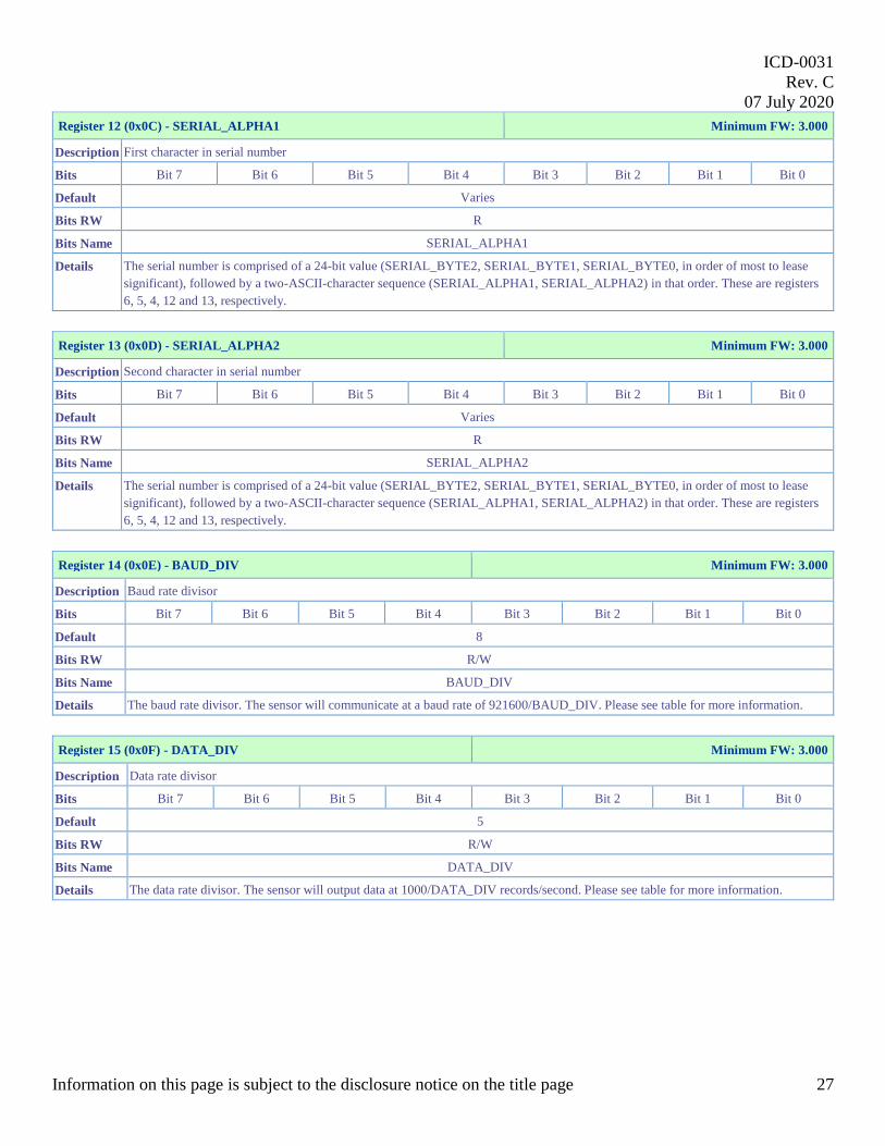
Register 12 (0x0C) - SERIAL_ALPHA1 Minimum FW: 3.000
Description First character in serial number
Bits Bit 7 Bit 6 Bit 5 Bit 4 Bit 3 Bit 2 Bit 1 Bit 0
Default Varies
Bits RW R
Bits Name SERIAL_ALPHA1
Details The serial number is comprised of a 24-bit value (SERIAL_BYTE2, SERIAL_BYTE1, SERIAL_BYTE0, in order of most to lease
significant), followed by a two-ASCII-character sequence (SERIAL_ALPHA1, SERIAL_ALPHA2) in that order. These are registers
6, 5, 4, 12 and 13, respectively.
Register 13 (0x0D) - SERIAL_ALPHA2 Minimum FW: 3.000
Description Second character in serial number
Bits Bit 7 Bit 6 Bit 5 Bit 4 Bit 3 Bit 2 Bit 1 Bit 0
Default Varies
Bits RW R
Bits Name SERIAL_ALPHA2
Details The serial number is comprised of a 24-bit value (SERIAL_BYTE2, SERIAL_BYTE1, SERIAL_BYTE0, in order of most to lease
significant), followed by a two-ASCII-character sequence (SERIAL_ALPHA1, SERIAL_ALPHA2) in that order. These are registers
6, 5, 4, 12 and 13, respectively.
Register 14 (0x0E) - BAUD_DIV Minimum FW: 3.000
Description Baud rate divisor
Bits Bit 7 Bit 6 Bit 5 Bit 4 Bit 3 Bit 2 Bit 1 Bit 0
Default 8
Bits RW R/W
Bits Name BAUD_DIV
Details The baud rate divisor. The sensor will communicate at a baud rate of 921600/BAUD_DIV. Please see table for more information.
Register 15 (0x0F) - DATA_DIV Minimum FW: 3.000
Description Data rate divisor
Bits Bit 7 Bit 6 Bit 5 Bit 4 Bit 3 Bit 2 Bit 1 Bit 0
Default 5
Bits RW R/W
Bits Name DATA_DIV
Details The data rate divisor. The sensor will output data at 1000/DATA_DIV records/second. Please see table for more information.
ICD-0031
Rev. C
07 July 2020
Information on this page is subject to the disclosure notice on the title page 28
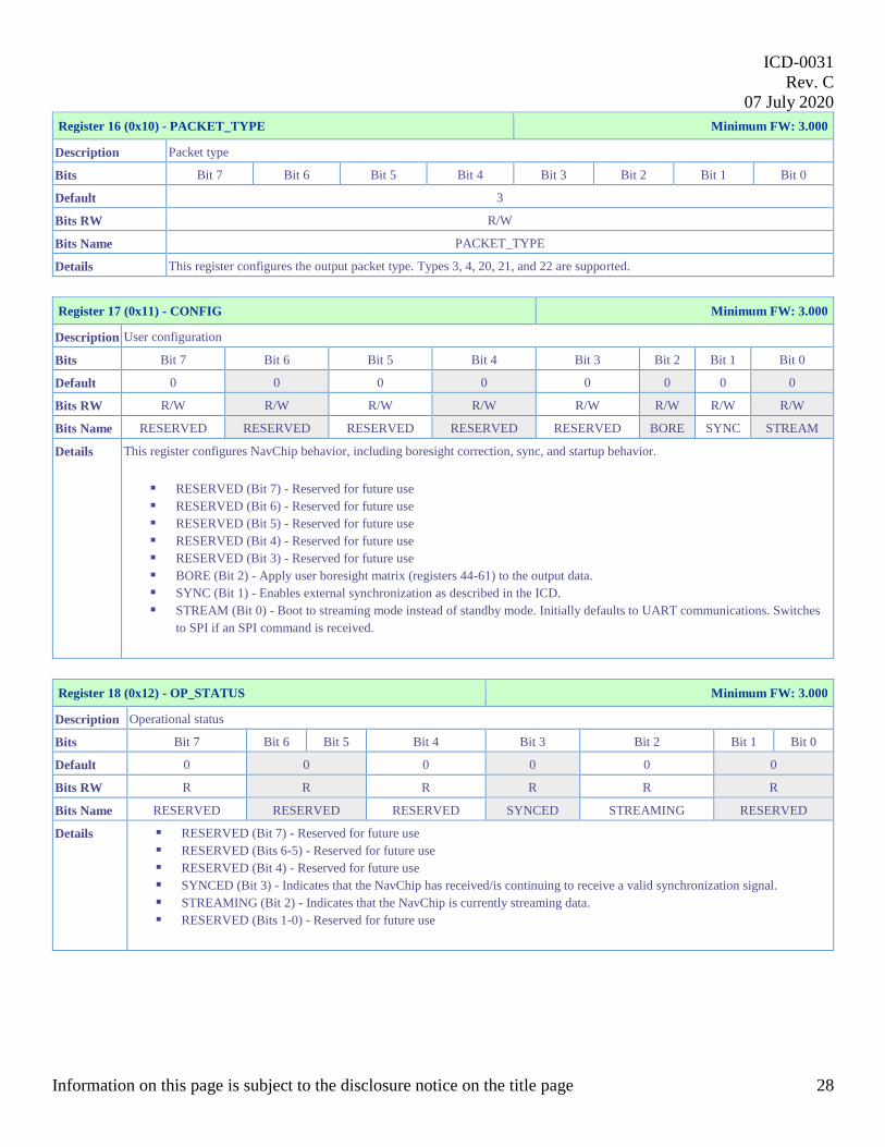
Register 16 (0x10) - PACKET_TYPE Minimum FW: 3.000
Description Packet type
Bits Bit 7 Bit 6 Bit 5 Bit 4 Bit 3 Bit 2 Bit 1 Bit 0
Default 3
Bits RW R/W
Bits Name PACKET_TYPE
Details This register configures the output packet type. Types 3, 4, 20, 21, and 22 are supported.
Register 17 (0x11) - CONFIG Minimum FW: 3.000
Description User configuration
Bits Bit 7 Bit 6 Bit 5 Bit 4 Bit 3 Bit 2 Bit 1 Bit 0
Default 0 0 0 0 0 0 0 0
Bits RW R/W R/W R/W R/W R/W R/W R/W R/W
Bits Name RESERVED RESERVED RESERVED RESERVED RESERVED BORE SYNC STREAM
Details This register configures NavChip behavior, including boresight correction, sync, and startup behavior.
RESERVED (Bit 7) - Reserved for future use
RESERVED (Bit 6) - Reserved for future use
RESERVED (Bit 5) - Reserved for future use
RESERVED (Bit 4) - Reserved for future use
RESERVED (Bit 3) - Reserved for future use
BORE (Bit 2) - Apply user boresight matrix (registers 44-61) to the output data.
SYNC (Bit 1) - Enables external synchronization as described in the ICD.
STREAM (Bit 0) - Boot to streaming mode instead of standby mode. Initially defaults to UART communications. Switches
to SPI if an SPI command is received.
Register 18 (0x12) - OP_STATUS Minimum FW: 3.000
Description Operational status
Bits Bit 7 Bit 6 Bit 5 Bit 4 Bit 3 Bit 2 Bit 1 Bit 0
Default 0 0 0 0 0 0
Bits RW R R R R R R
Bits Name RESERVED RESERVED RESERVED SYNCED STREAMING RESERVED
Details RESERVED (Bit 7) - Reserved for future use
RESERVED (Bits 6-5) - Reserved for future use
RESERVED (Bit 4) - Reserved for future use
SYNCED (Bit 3) - Indicates that the NavChip has received/is continuing to receive a valid synchronization signal.
STREAMING (Bit 2) - Indicates that the NavChip is currently streaming data.
RESERVED (Bits 1-0) - Reserved for future use
ICD-0031
Rev. C
07 July 2020
Information on this page is subject to the disclosure notice on the title page 29
Register 20 (0x14) - VIN_I Minimum FW: 3.000
Description VIN sense current
Bits Bit 7 Bit 6 Bit 5 Bit 4 Bit 3 Bit 2 Bit 1 Bit 0
Default 0
Bits RW R
Bits Name VIN_I
Details VIN sense current as reported by the on-board current sensor. Resolution 0.5 mA/LSB
Register 21 (0x15) - VDD_I Minimum FW: 3.000
Description VDD2 sense current
Bits Bit 7 Bit 6 Bit 5 Bit 4 Bit 3 Bit 2 Bit 1 Bit 0
Default 0
Bits RW R
Bits Name VDD_I
Details VDD sense current as reported by the on-board current sensor. Resolution 0.5 mA/LSB
Register 22 (0x16) - VDD2_I Minimum FW: 3.000
Description VDD2 sense current
Bits Bit 7 Bit 6 Bit 5 Bit 4 Bit 3 Bit 2 Bit 1 Bit 0
Default 0
Bits RW R
Bits Name VDD2_I
Details VDD2 sense current as reported by the on-board current sensor. Resolution 0.5 mA/LSB

ICD-0031
Rev. C
07 July 2020
Information on this page is subject to the disclosure notice on the title page 30
Register 23 (0x17) - RUNTIME_WARN Minimum FW: 3.000
Description Runtime warning flags
elayBits Bit 7 Bit 6 Bit 5 Bit 4 Bit 3 Bit 2 Bit 1 Bit 0
Default 0 0 0 0 0 0 0 0
Bits RW R R R R R R R R
Bits Name CURRENT SYNCFAIL INTEG VOLT TEMP MAG ACCEL GYRO
Details Runtime warning flags indicate that a problem has occurred with the NavChip (not a typical occurrence), or provide status information
in the case of the two sync bits. In some cases, such as a failure of gyro or accelerometer data, this may cause the output data to stop
updating (this could happen if the NavChip was physically damaged by an extreme impact, for instance). It is recommended that this
register be read periodically (i.e. using the S-bits that are output once per frame) to detect any problems soon after they occur.
CURRENT (Bit 7) - Indicates an overcurrent condition has been detected. Clears automatically upon current returning to
acceptable range.
SYNCFAIL (Bit 6) - Indicates a fault with synchronization (sync is enabled, but the sync signal has been missing or invalid
for a period of time).
INTEG (Bit 5) - Indicates an internal fault with sensor sampling. Accel/gyro/mag data may be invalid.
VOLT (Bit 4) - Indicates that the supply voltage is out of range. Streaming output will be suppressed or terminated. Clears
automatically upon voltage returning to factory-calibrated range.
TEMP (Bit 3) - Indicates that the temperature has exceeded the calibrated temperature range. Streaming output will be
suppressed or terminated. Clears automatically upon temperature returning to factory-calibrated range.
MAG (Bit 2) - Indicates that a problem has been detected with magnetometer data during CBIT.
ACCEL (Bit 1) - Indicates that a problem has been detected with accelerometer data during CBIT.
GYRO (Bit 0) - Indicates that a problem has been detected with gyroscope data during CBIT.
Register 25 (0x19) - ENVIRO_0 Minimum FW: 3.000
Description Environmental data register 0
Bits Bit 7 Bit 6 Bit 5 Bit 4 Bit 3 Bit 2 Bit 1 Bit 0
Default Varies
Bits RW R
Bits Name VIN_BITS_7_0
Details Contains information about the environment the sensor is operating in.
VIN_BITS_7_0 (Bits 7-0) - A portion of the 12-bit input voltage data. Input voltage (maximum of 6.0V) is 1.4648e-3 *
((VIN_BITS_11_4 << 4) | VIN_BITS_3_0).
ICD-0031
Rev. C
07 July 2020
Information on this page is subject to the disclosure notice on the title page 31
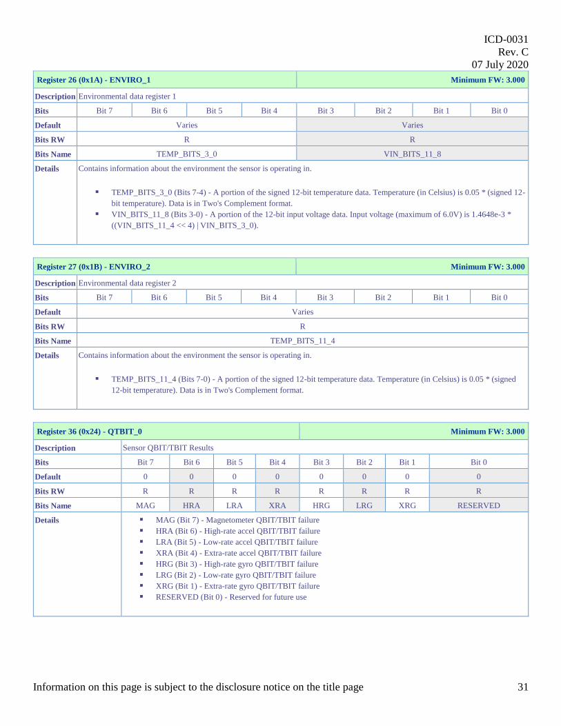
Register 26 (0x1A) - ENVIRO_1 Minimum FW: 3.000
Description Environmental data register 1
Bits Bit 7 Bit 6 Bit 5 Bit 4 Bit 3 Bit 2 Bit 1 Bit 0
Default Varies Varies
Bits RW R R
Bits Name TEMP_BITS_3_0 VIN_BITS_11_8
Details Contains information about the environment the sensor is operating in.
TEMP_BITS_3_0 (Bits 7-4) - A portion of the signed 12-bit temperature data. Temperature (in Celsius) is 0.05 * (signed 12-
bit temperature). Data is in Two's Complement format.
VIN_BITS_11_8 (Bits 3-0) - A portion of the 12-bit input voltage data. Input voltage (maximum of 6.0V) is 1.4648e-3 *
((VIN_BITS_11_4 << 4) | VIN_BITS_3_0).
Register 27 (0x1B) - ENVIRO_2 Minimum FW: 3.000
Description Environmental data register 2
Bits Bit 7 Bit 6 Bit 5 Bit 4 Bit 3 Bit 2 Bit 1 Bit 0
Default Varies
Bits RW R
Bits Name TEMP_BITS_11_4
Details Contains information about the environment the sensor is operating in.
TEMP_BITS_11_4 (Bits 7-0) - A portion of the signed 12-bit temperature data. Temperature (in Celsius) is 0.05 * (signed
12-bit temperature). Data is in Two's Complement format.
Register 36 (0x24) - QTBIT_0 Minimum FW: 3.000
Description Sensor QBIT/TBIT Results
Bits Bit 7 Bit 6 Bit 5 Bit 4 Bit 3 Bit 2 Bit 1 Bit 0
Default 0 0 0 0 0 0 0 0
Bits RW R R R R R R R R
Bits Name MAG HRA LRA XRA HRG LRG XRG RESERVED
Details MAG (Bit 7) - Magnetometer QBIT/TBIT failure
HRA (Bit 6) - High-rate accel QBIT/TBIT failure
LRA (Bit 5) - Low-rate accel QBIT/TBIT failure
XRA (Bit 4) - Extra-rate accel QBIT/TBIT failure
HRG (Bit 3) - High-rate gyro QBIT/TBIT failure
LRG (Bit 2) - Low-rate gyro QBIT/TBIT failure
XRG (Bit 1) - Extra-rate gyro QBIT/TBIT failure
RESERVED (Bit 0) - Reserved for future use
ICD-0031
Rev. C
07 July 2020
Information on this page is subject to the disclosure notice on the title page 32
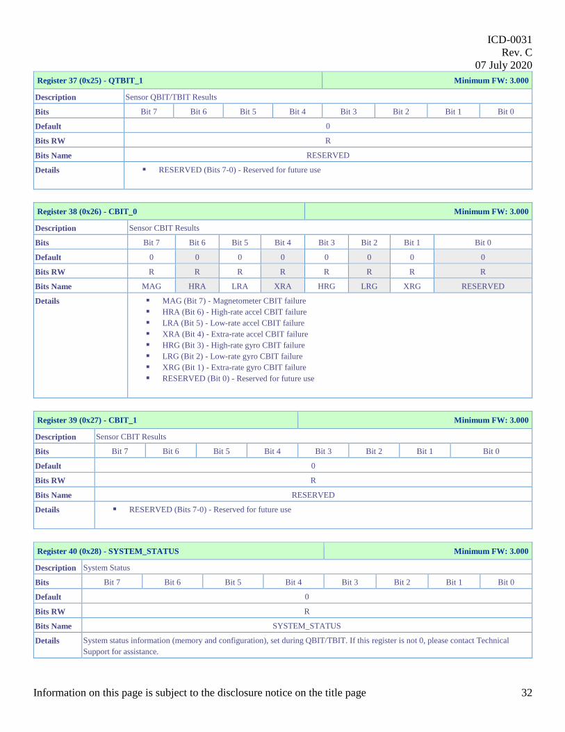
Register 37 (0x25) - QTBIT_1 Minimum FW: 3.000
Description Sensor QBIT/TBIT Results
Bits Bit 7 Bit 6 Bit 5 Bit 4 Bit 3 Bit 2 Bit 1 Bit 0
Default 0
Bits RW R
Bits Name RESERVED
Details RESERVED (Bits 7-0) - Reserved for future use
Register 38 (0x26) - CBIT_0 Minimum FW: 3.000
Description Sensor CBIT Results
Bits Bit 7 Bit 6 Bit 5 Bit 4 Bit 3 Bit 2 Bit 1 Bit 0
Default 0 0 0 0 0 0 0 0
Bits RW R R R R R R R R
Bits Name MAG HRA LRA XRA HRG LRG XRG RESERVED
Details MAG (Bit 7) - Magnetometer CBIT failure
HRA (Bit 6) - High-rate accel CBIT failure
LRA (Bit 5) - Low-rate accel CBIT failure
XRA (Bit 4) - Extra-rate accel CBIT failure
HRG (Bit 3) - High-rate gyro CBIT failure
LRG (Bit 2) - Low-rate gyro CBIT failure
XRG (Bit 1) - Extra-rate gyro CBIT failure
RESERVED (Bit 0) - Reserved for future use
Register 39 (0x27) - CBIT_1 Minimum FW: 3.000
Description Sensor CBIT Results
Bits Bit 7 Bit 6 Bit 5 Bit 4 Bit 3 Bit 2 Bit 1 Bit 0
Default 0
Bits RW R
Bits Name RESERVED
Details RESERVED (Bits 7-0) - Reserved for future use
Register 40 (0x28) - SYSTEM_STATUS Minimum FW: 3.000
Description System Status
Bits Bit 7 Bit 6 Bit 5 Bit 4 Bit 3 Bit 2 Bit 1 Bit 0
Default 0
Bits RW R
Bits Name SYSTEM_STATUS
Details System status information (memory and configuration), set during QBIT/TBIT. If this register is not 0, please contact Technical
Support for assistance.
ICD-0031
Rev. C
07 July 2020
Information on this page is subject to the disclosure notice on the title page 33
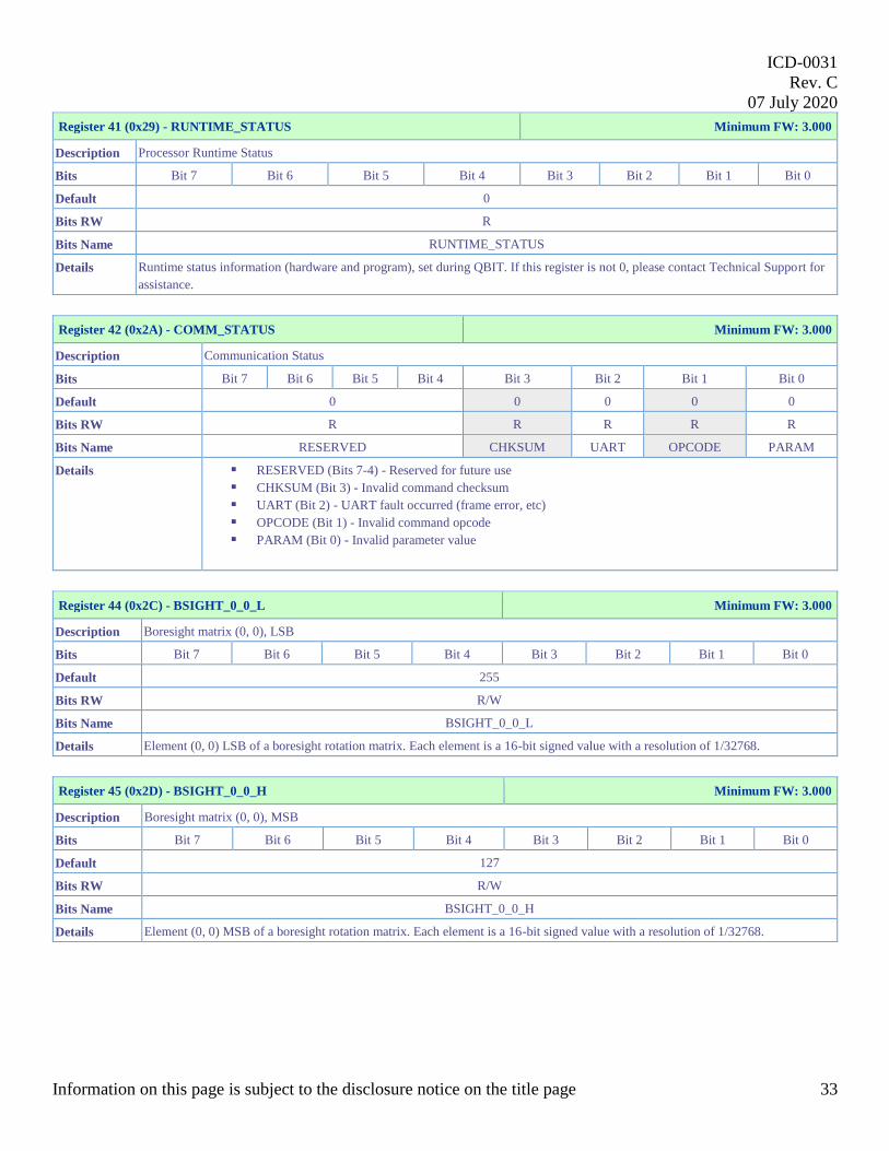
Register 41 (0x29) - RUNTIME_STATUS Minimum FW: 3.000
Description Processor Runtime Status
Bits Bit 7 Bit 6 Bit 5 Bit 4 Bit 3 Bit 2 Bit 1 Bit 0
Default 0
Bits RW R
Bits Name RUNTIME_STATUS
Details Runtime status information (hardware and program), set during QBIT. If this register is not 0, please contact Technical Support for
assistance.
Register 42 (0x2A) - COMM_STATUS Minimum FW: 3.000
Description Communication Status
Bits Bit 7 Bit 6 Bit 5 Bit 4 Bit 3 Bit 2 Bit 1 Bit 0
Default 0 0 0 0 0
Bits RW R R R R R
Bits Name RESERVED CHKSUM UART OPCODE PARAM
Details RESERVED (Bits 7-4) - Reserved for future use
CHKSUM (Bit 3) - Invalid command checksum
UART (Bit 2) - UART fault occurred (frame error, etc)
OPCODE (Bit 1) - Invalid command opcode
PARAM (Bit 0) - Invalid parameter value
Register 44 (0x2C) - BSIGHT_0_0_L Minimum FW: 3.000
Description Boresight matrix (0, 0), LSB
Bits Bit 7 Bit 6 Bit 5 Bit 4 Bit 3 Bit 2 Bit 1 Bit 0
Default 255
Bits RW R/W
Bits Name BSIGHT_0_0_L
Details Element (0, 0) LSB of a boresight rotation matrix. Each element is a 16-bit signed value with a resolution of 1/32768.
Register 45 (0x2D) - BSIGHT_0_0_H Minimum FW: 3.000
Description Boresight matrix (0, 0), MSB
Bits Bit 7 Bit 6 Bit 5 Bit 4 Bit 3 Bit 2 Bit 1 Bit 0
Default 127
Bits RW R/W
Bits Name BSIGHT_0_0_H
Details Element (0, 0) MSB of a boresight rotation matrix. Each element is a 16-bit signed value with a resolution of 1/32768.
ICD-0031
Rev. C
07 July 2020
Information on this page is subject to the disclosure notice on the title page 34
Register 46 (0x2E) - BSIGHT_0_1_L Minimum FW: 3.000
Description Boresight matrix (0, 1), LSB
Bits Bit 7 Bit 6 Bit 5 Bit 4 Bit 3 Bit 2 Bit 1 Bit 0
Default 0
Bits RW R/W
Bits Name BSIGHT_0_1_L
Details Element (0, 1) LSB of a boresight rotation matrix. Each element is a 16-bit signed value with a resolution of 1/32768.
Register 47 (0x2F) - BSIGHT_0_1_H Minimum FW: 3.000
Description Boresight matrix (0, 1), MSB
Bits Bit 7 Bit 6 Bit 5 Bit 4 Bit 3 Bit 2 Bit 1 Bit 0
Default 0
Bits RW R/W
Bits Name BSIGHT_0_1_H
Details Element (0, 1) MSB of a boresight rotation matrix. Each element is a 16-bit signed value with a resolution of 1/32768.
Register 48 (0x30) - BSIGHT_0_2_L Minimum FW: 3.000
Description Boresight matrix (0, 2), LSB
Bits Bit 7 Bit 6 Bit 5 Bit 4 Bit 3 Bit 2 Bit 1 Bit 0
Default 0
Bits RW R/W
Bits Name BSIGHT_0_2_L
Details Element (0, 2) LSB of a boresight rotation matrix. Each element is a 16-bit signed value with a resolution of 1/32768.
Register 49 (0x31) - BSIGHT_0_2_H Minimum FW: 3.000
Description Boresight matrix (0, 2), MSB
Bits Bit 7 Bit 6 Bit 5 Bit 4 Bit 3 Bit 2 Bit 1 Bit 0
Default 0
Bits RW R/W
Bits Name BSIGHT_0_2_H
Details Element (0, 2) MSB of a boresight rotation matrix. Each element is a 16-bit signed value with a resolution of 1/32768.
Register 50 (0x32) - BSIGHT_1_0_L Minimum FW: 3.000
Description Boresight matrix (1, 0), LSB
Bits Bit 7 Bit 6 Bit 5 Bit 4 Bit 3 Bit 2 Bit 1 Bit 0
Default 0
Bits RW R/W
Bits Name BSIGHT_1_0_L
Details Element (1, 0) LSB of a boresight rotation matrix. Each element is a 16-bit signed value with a resolution of 1/32768.
ICD-0031
Rev. C
07 July 2020
Information on this page is subject to the disclosure notice on the title page 35
Register 51 (0x33) - BSIGHT_1_0_H Minimum FW: 3.000
Description Boresight matrix (1, 0), MSB
Bits Bit 7 Bit 6 Bit 5 Bit 4 Bit 3 Bit 2 Bit 1 Bit 0
Default 0
Bits RW R/W
Bits Name BSIGHT_1_0_H
Details Element (1, 0) MSB of a boresight rotation matrix. Each element is a 16-bit signed value with a resolution of 1/32768.
Register 52 (0x34) - BSIGHT_1_1_L Minimum FW: 3.000
Description Boresight matrix (1, 1), LSB
Bits Bit 7 Bit 6 Bit 5 Bit 4 Bit 3 Bit 2 Bit 1 Bit 0
Default 255
Bits RW R/W
Bits Name BSIGHT_1_1_L
Details Element (1, 1) LSB of a boresight rotation matrix. Each element is a 16-bit signed value with a resolution of 1/32768.
Register 53 (0x35) - BSIGHT_1_1_H Minimum FW: 3.000
Description Boresight matrix (1, 1), MSB
Bits Bit 7 Bit 6 Bit 5 Bit 4 Bit 3 Bit 2 Bit 1 Bit 0
Default 127
Bits RW R/W
Bits Name BSIGHT_1_1_H
Details Element (1, 1) MSB of a boresight rotation matrix. Each element is a 16-bit signed value with a resolution of 1/32768.
Register 54 (0x36) - BSIGHT_1_2_L Minimum FW: 3.000
Description Boresight matrix (1, 2), LSB
Bits Bit 7 Bit 6 Bit 5 Bit 4 Bit 3 Bit 2 Bit 1 Bit 0
Default 0
Bits RW R/W
Bits Name BSIGHT_1_2_L
Details Element (1, 2) LSB of a boresight rotation matrix. Each element is a 16-bit signed value with a resolution of 1/32768.
Register 55 (0x37) - BSIGHT_1_2_H Minimum FW: 3.000
Description Boresight matrix (1, 2), MSB
Bits Bit 7 Bit 6 Bit 5 Bit 4 Bit 3 Bit 2 Bit 1 Bit 0
Default 0
Bits RW R/W
Bits Name BSIGHT_1_2_H
Details Element (1, 2) MSB of a boresight rotation matrix. Each element is a 16-bit signed value with a resolution of 1/32768.
ICD-0031
Rev. C
07 July 2020
Information on this page is subject to the disclosure notice on the title page 36
Register 56 (0x38) - BSIGHT_2_0_L Minimum FW: 3.000
Description Boresight matrix (2, 0), LSB
Bits Bit 7 Bit 6 Bit 5 Bit 4 Bit 3 Bit 2 Bit 1 Bit 0
Default 0
Bits RW R/W
Bits Name BSIGHT_2_0_L
Details Element (2, 0) LSB of a boresight rotation matrix. Each element is a 16-bit signed value with a resolution of 1/32768.
Register 57 (0x39) - BSIGHT_2_0_H Minimum FW: 3.000
Description Boresight matrix (2, 0), MSB
Bits Bit 7 Bit 6 Bit 5 Bit 4 Bit 3 Bit 2 Bit 1 Bit 0
Default 0
Bits RW R/W
Bits Name BSIGHT_2_0_H
Details Element (2, 0) MSB of a boresight rotation matrix. Each element is a 16-bit signed value with a resolution of 1/32768.
Register 58 (0x3A) - BSIGHT_2_1_L Minimum FW: 3.000
Description Boresight matrix (2, 1), LSB
Bits Bit 7 Bit 6 Bit 5 Bit 4 Bit 3 Bit 2 Bit 1 Bit 0
Default 0
Bits RW R/W
Bits Name BSIGHT_2_1_L
Details Element (2, 1) LSB of a boresight rotation matrix. Each element is a 16-bit signed value with a resolution of 1/32768.
Register 59 (0x3B) - BSIGHT_2_1_H Minimum FW: 3.000
Description Boresight matrix (2, 1), MSB
Bits Bit 7 Bit 6 Bit 5 Bit 4 Bit 3 Bit 2 Bit 1 Bit 0
Default 0
Bits RW R/W
Bits Name BSIGHT_2_1_H
Details Element (2, 1) MSB of a boresight rotation matrix. Each element is a 16-bit signed value with a resolution of 1/32768.
Register 60 (0x3C) - BSIGHT_2_2_L Minimum FW: 3.000
Description Boresight matrix (2, 2), LSB
Bits Bit 7 Bit 6 Bit 5 Bit 4 Bit 3 Bit 2 Bit 1 Bit 0
Default 255
Bits RW R/W
Bits Name BSIGHT_2_2_L
Details Element (2, 2) LSB of a boresight rotation matrix. Each element is a 16-bit signed value with a resolution of 1/32768.
ICD-0031
Rev. C
07 July 2020
Information on this page is subject to the disclosure notice on the title page 37
Register 61 (0x3D) - BSIGHT_2_2_H Minimum FW: 3.000
Description Boresight matrix (2, 2), MSB
Bits Bit 7 Bit 6 Bit 5 Bit 4 Bit 3 Bit 2 Bit 1 Bit 0
Default 127
Bits RW R/W
Bits Name BSIGHT_2_2_H
Details Element (2, 2) MSB of a boresight rotation matrix. Each element is a 16-bit signed value with a resolution of 1/32768.
Register 62 (0x3E) - MAG_HI_0_L Minimum FW: 3.000
Description Mag hard iron bias X, LSB
Bits Bit 7 Bit 6 Bit 5 Bit 4 Bit 3 Bit 2 Bit 1 Bit 0
Default 0
Bits RW R/W
Bits Name MAG_HI_0_L
Details X magnetometer bias offset in Gauss, LSB. Each element is a 16-bit signed value with a resolution of 1/(2^13), with a range of
approximately +4 to -4. Currently set/used by the DLL only (when set to a value other than 0, on NavChips with magnetometers), and
not applied by the NavChip, though later firmware versions may apply it directly. Currently set/used by the DLL only (when set to a
value other than 0, on NavChips with magnetometers), and not applied by the NavChip, though later firmware versions may apply it
directly.
Register 63 (0x3F) - MAG_HI_0_H Minimum FW: 3.000
Description Mag hard iron bias X, MSB
Bits Bit 7 Bit 6 Bit 5 Bit 4 Bit 3 Bit 2 Bit 1 Bit 0
Default 0
Bits RW R/W
Bits Name MAG_HI_0_H
Details X magnetometer bias offset in Gauss, MSB. Each element is a 16-bit signed value with a resolution of 1/(2^13), with a range of
approximately +4 to -4. Currently set/used by the DLL only (when set to a value other than 0, on NavChips with magnetometers), and
not applied by the NavChip, though later firmware versions may apply it directly.
Register 64 (0x40) - MAG_HI_1_L Minimum FW: 3.000
Description Mag hard iron bias Y, LSB
Bits Bit 7 Bit 6 Bit 5 Bit 4 Bit 3 Bit 2 Bit 1 Bit 0
Default 0
Bits RW R/W
Bits Name MAG_HI_1_L
Details Y magnetometer bias offset in Gauss, LSB. Each element is a 16-bit signed value with a resolution of 1/(2^13), with a range of
approximately +4 to -4. Currently set/used by the DLL only (when set to a value other than 0, on NavChips with magnetometers), and
not applied by the NavChip, though later firmware versions may apply it directly.
ICD-0031
Rev. C
07 July 2020
Information on this page is subject to the disclosure notice on the title page 38
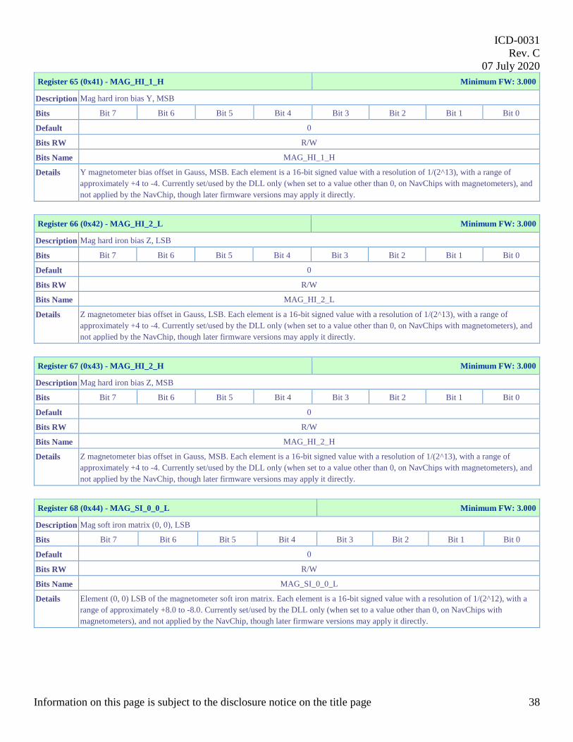
Register 65 (0x41) - MAG_HI_1_H Minimum FW: 3.000
Description Mag hard iron bias Y, MSB
Bits Bit 7 Bit 6 Bit 5 Bit 4 Bit 3 Bit 2 Bit 1 Bit 0
Default 0
Bits RW R/W
Bits Name MAG_HI_1_H
Details Y magnetometer bias offset in Gauss, MSB. Each element is a 16-bit signed value with a resolution of 1/(2^13), with a range of
approximately +4 to -4. Currently set/used by the DLL only (when set to a value other than 0, on NavChips with magnetometers), and
not applied by the NavChip, though later firmware versions may apply it directly.
Register 66 (0x42) - MAG_HI_2_L Minimum FW: 3.000
Description Mag hard iron bias Z, LSB
Bits Bit 7 Bit 6 Bit 5 Bit 4 Bit 3 Bit 2 Bit 1 Bit 0
Default 0
Bits RW R/W
Bits Name MAG_HI_2_L
Details Z magnetometer bias offset in Gauss, LSB. Each element is a 16-bit signed value with a resolution of 1/(2^13), with a range of
approximately +4 to -4. Currently set/used by the DLL only (when set to a value other than 0, on NavChips with magnetometers), and
not applied by the NavChip, though later firmware versions may apply it directly.
Register 67 (0x43) - MAG_HI_2_H Minimum FW: 3.000
Description Mag hard iron bias Z, MSB
Bits Bit 7 Bit 6 Bit 5 Bit 4 Bit 3 Bit 2 Bit 1 Bit 0
Default 0
Bits RW R/W
Bits Name MAG_HI_2_H
Details Z magnetometer bias offset in Gauss, MSB. Each element is a 16-bit signed value with a resolution of 1/(2^13), with a range of
approximately +4 to -4. Currently set/used by the DLL only (when set to a value other than 0, on NavChips with magnetometers), and
not applied by the NavChip, though later firmware versions may apply it directly.
Register 68 (0x44) - MAG_SI_0_0_L Minimum FW: 3.000
Description Mag soft iron matrix (0, 0), LSB
Bits Bit 7 Bit 6 Bit 5 Bit 4 Bit 3 Bit 2 Bit 1 Bit 0
Default 0
Bits RW R/W
Bits Name MAG_SI_0_0_L
Details Element (0, 0) LSB of the magnetometer soft iron matrix. Each element is a 16-bit signed value with a resolution of 1/(2^12), with a
range of approximately +8.0 to -8.0. Currently set/used by the DLL only (when set to a value other than 0, on NavChips with
magnetometers), and not applied by the NavChip, though later firmware versions may apply it directly.
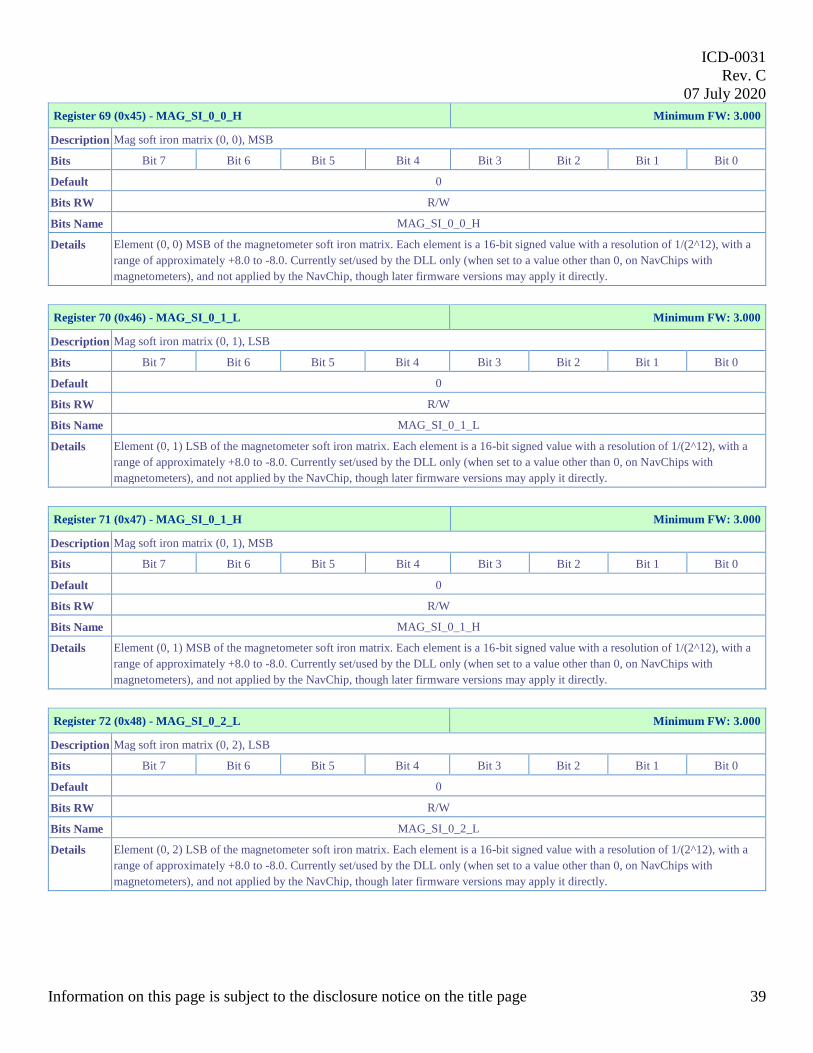
ICD-0031
Rev. C
07 July 2020
Information on this page is subject to the disclosure notice on the title page 39
Register 69 (0x45) - MAG_SI_0_0_H Minimum FW: 3.000
Description Mag soft iron matrix (0, 0), MSB
Bits Bit 7 Bit 6 Bit 5 Bit 4 Bit 3 Bit 2 Bit 1 Bit 0
Default 0
Bits RW R/W
Bits Name MAG_SI_0_0_H
Details Element (0, 0) MSB of the magnetometer soft iron matrix. Each element is a 16-bit signed value with a resolution of 1/(2^12), with a
range of approximately +8.0 to -8.0. Currently set/used by the DLL only (when set to a value other than 0, on NavChips with
magnetometers), and not applied by the NavChip, though later firmware versions may apply it directly.
Register 70 (0x46) - MAG_SI_0_1_L Minimum FW: 3.000
Description Mag soft iron matrix (0, 1), LSB
Bits Bit 7 Bit 6 Bit 5 Bit 4 Bit 3 Bit 2 Bit 1 Bit 0
Default 0
Bits RW R/W
Bits Name MAG_SI_0_1_L
Details Element (0, 1) LSB of the magnetometer soft iron matrix. Each element is a 16-bit signed value with a resolution of 1/(2^12), with a
range of approximately +8.0 to -8.0. Currently set/used by the DLL only (when set to a value other than 0, on NavChips with
magnetometers), and not applied by the NavChip, though later firmware versions may apply it directly.
Register 71 (0x47) - MAG_SI_0_1_H Minimum FW: 3.000
Description Mag soft iron matrix (0, 1), MSB
Bits Bit 7 Bit 6 Bit 5 Bit 4 Bit 3 Bit 2 Bit 1 Bit 0
Default 0
Bits RW R/W
Bits Name MAG_SI_0_1_H
Details Element (0, 1) MSB of the magnetometer soft iron matrix. Each element is a 16-bit signed value with a resolution of 1/(2^12), with a
range of approximately +8.0 to -8.0. Currently set/used by the DLL only (when set to a value other than 0, on NavChips with
magnetometers), and not applied by the NavChip, though later firmware versions may apply it directly.
Register 72 (0x48) - MAG_SI_0_2_L Minimum FW: 3.000
Description Mag soft iron matrix (0, 2), LSB
Bits Bit 7 Bit 6 Bit 5 Bit 4 Bit 3 Bit 2 Bit 1 Bit 0
Default 0
Bits RW R/W
Bits Name MAG_SI_0_2_L
Details Element (0, 2) LSB of the magnetometer soft iron matrix. Each element is a 16-bit signed value with a resolution of 1/(2^12), with a
range of approximately +8.0 to -8.0. Currently set/used by the DLL only (when set to a value other than 0, on NavChips with
magnetometers), and not applied by the NavChip, though later firmware versions may apply it directly.

ICD-0031
Rev. C
07 July 2020
Information on this page is subject to the disclosure notice on the title page 40
Register 73 (0x49) - MAG_SI_0_2_H Minimum FW: 3.000
Description Mag soft iron matrix (0, 2), MSB
Bits Bit 7 Bit 6 Bit 5 Bit 4 Bit 3 Bit 2 Bit 1 Bit 0
Default 0
Bits RW R/W
Bits Name MAG_SI_0_2_H
Details Element (0, 2) MSB of the magnetometer soft iron matrix. Each element is a 16-bit signed value with a resolution of 1/(2^12), with a
range of approximately +8.0 to -8.0. Currently set/used by the DLL only (when set to a value other than 0, on NavChips with
magnetometers), and not applied by the NavChip, though later firmware versions may apply it directly.
Register 74 (0x4A) - MAG_SI_1_0_L Minimum FW: 3.000
Description Mag soft iron matrix (1, 0), LSB
Bits Bit 7 Bit 6 Bit 5 Bit 4 Bit 3 Bit 2 Bit 1 Bit 0
Default 0
Bits RW R/W
Bits Name MAG_SI_1_0_L
Details Element (1, 0) LSB of the magnetometer soft iron matrix. Each element is a 16-bit signed value with a resolution of 1/(2^12), with a
range of approximately +8.0 to -8.0. Currently set/used by the DLL only (when set to a value other than 0, on NavChips with
magnetometers), and not applied by the NavChip, though later firmware versions may apply it directly.
Register 75 (0x4B) - MAG_SI_1_0_H Minimum FW: 3.000
Description Mag soft iron matrix (1, 0), MSB
Bits Bit 7 Bit 6 Bit 5 Bit 4 Bit 3 Bit 2 Bit 1 Bit 0
Default 0
Bits RW R/W
Bits Name MAG_SI_1_0_H
Details Element (1, 0) MSB of the magnetometer soft iron matrix. Each element is a 16-bit signed value with a resolution of 1/(2^12), with a
range of approximately +8.0 to -8.0. Currently set/used by the DLL only (when set to a value other than 0, on NavChips with
magnetometers), and not applied by the NavChip, though later firmware versions may apply it directly.
Register 76 (0x4C) - MAG_SI_1_1_L Minimum FW: 3.000
Description Mag soft iron matrix (1, 1), LSB
Bits Bit 7 Bit 6 Bit 5 Bit 4 Bit 3 Bit 2 Bit 1 Bit 0
Default 0
Bits RW R/W
Bits Name MAG_SI_1_1_L
Details Element (1, 1) LSB of the magnetometer soft iron matrix. Each element is a 16-bit signed value with a resolution of 1/(2^12), with a
range of approximately +8.0 to -8.0. Currently set/used by the DLL only (when set to a value other than 0, on NavChips with
magnetometers), and not applied by the NavChip, though later firmware versions may apply it directly.

ICD-0031
Rev. C
07 July 2020
Information on this page is subject to the disclosure notice on the title page 41
Register 77 (0x4D) - MAG_SI_1_1_H Minimum FW: 3.000
Description Mag soft iron matrix (1, 1), MSB
Bits Bit 7 Bit 6 Bit 5 Bit 4 Bit 3 Bit 2 Bit 1 Bit 0
Default 0
Bits RW R/W
Bits Name MAG_SI_1_1_H
Details Element (1, 1) MSB of the magnetometer soft iron matrix. Each element is a 16-bit signed value with a resolution of 1/(2^12), with a
range of approximately +8.0 to -8.0. Currently set/used by the DLL only (when set to a value other than 0, on NavChips with
magnetometers), and not applied by the NavChip, though later firmware versions may apply it directly.
Register 78 (0x4E) - MAG_SI_1_2_L Minimum FW: 3.000
Description Mag soft iron matrix (1, 2), LSB
Bits Bit 7 Bit 6 Bit 5 Bit 4 Bit 3 Bit 2 Bit 1 Bit 0
Default 0
Bits RW R/W
Bits Name MAG_SI_1_2_L
Details Element (1, 2) LSB of the magnetometer soft iron matrix. Each element is a 16-bit signed value with a resolution of 1/(2^12), with a
range of approximately +8.0 to -8.0. Currently set/used by the DLL only (when set to a value other than 0, on NavChips with
magnetometers), and not applied by the NavChip, though later firmware versions may apply it directly.
Register 79 (0x4F) - MAG_SI_1_2_H Minimum FW: 3.000
Description Mag soft iron matrix (1, 2), MSB
Bits Bit 7 Bit 6 Bit 5 Bit 4 Bit 3 Bit 2 Bit 1 Bit 0
Default 0
Bits RW R/W
Bits Name MAG_SI_1_2_H
Details Element (1, 2) MSB of the magnetometer soft iron matrix. Each element is a 16-bit signed value with a resolution of 1/(2^12), with a
range of approximately +8.0 to -8.0. Currently set/used by the DLL only (when set to a value other than 0, on NavChips with
magnetometers), and not applied by the NavChip, though later firmware versions may apply it directly.
Register 80 (0x50) - MAG_SI_2_0_L Minimum FW: 3.000
Description Mag soft iron matrix (2, 0), LSB
Bits Bit 7 Bit 6 Bit 5 Bit 4 Bit 3 Bit 2 Bit 1 Bit 0
Default 0
Bits RW R/W
Bits Name MAG_SI_2_0_L
Details Element (2, 0) LSB of the magnetometer soft iron matrix. Each element is a 16-bit signed value with a resolution of 1/(2^12), with a
range of approximately +8.0 to -8.0. Currently set/used by the DLL only (when set to a value other than 0, on NavChips with
magnetometers), and not applied by the NavChip, though later firmware versions may apply it directly.
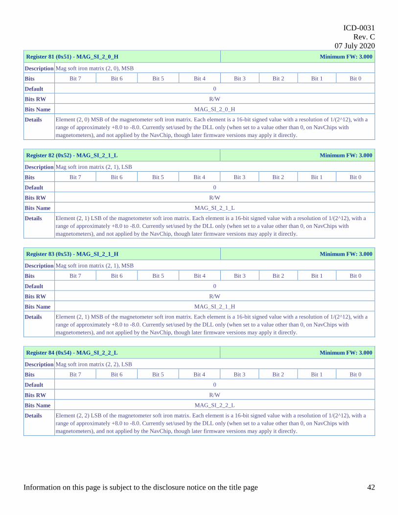
ICD-0031
Rev. C
07 July 2020
Information on this page is subject to the disclosure notice on the title page 42
Register 81 (0x51) - MAG_SI_2_0_H Minimum FW: 3.000
Description Mag soft iron matrix (2, 0), MSB
Bits Bit 7 Bit 6 Bit 5 Bit 4 Bit 3 Bit 2 Bit 1 Bit 0
Default 0
Bits RW R/W
Bits Name MAG_SI_2_0_H
Details Element (2, 0) MSB of the magnetometer soft iron matrix. Each element is a 16-bit signed value with a resolution of 1/(2^12), with a
range of approximately +8.0 to -8.0. Currently set/used by the DLL only (when set to a value other than 0, on NavChips with
magnetometers), and not applied by the NavChip, though later firmware versions may apply it directly.
Register 82 (0x52) - MAG_SI_2_1_L Minimum FW: 3.000
Description Mag soft iron matrix (2, 1), LSB
Bits Bit 7 Bit 6 Bit 5 Bit 4 Bit 3 Bit 2 Bit 1 Bit 0
Default 0
Bits RW R/W
Bits Name MAG_SI_2_1_L
Details Element (2, 1) LSB of the magnetometer soft iron matrix. Each element is a 16-bit signed value with a resolution of 1/(2^12), with a
range of approximately +8.0 to -8.0. Currently set/used by the DLL only (when set to a value other than 0, on NavChips with
magnetometers), and not applied by the NavChip, though later firmware versions may apply it directly.
Register 83 (0x53) - MAG_SI_2_1_H Minimum FW: 3.000
Description Mag soft iron matrix (2, 1), MSB
Bits Bit 7 Bit 6 Bit 5 Bit 4 Bit 3 Bit 2 Bit 1 Bit 0
Default 0
Bits RW R/W
Bits Name MAG_SI_2_1_H
Details Element (2, 1) MSB of the magnetometer soft iron matrix. Each element is a 16-bit signed value with a resolution of 1/(2^12), with a
range of approximately +8.0 to -8.0. Currently set/used by the DLL only (when set to a value other than 0, on NavChips with
magnetometers), and not applied by the NavChip, though later firmware versions may apply it directly.
Register 84 (0x54) - MAG_SI_2_2_L Minimum FW: 3.000
Description Mag soft iron matrix (2, 2), LSB
Bits Bit 7 Bit 6 Bit 5 Bit 4 Bit 3 Bit 2 Bit 1 Bit 0
Default 0
Bits RW R/W
Bits Name MAG_SI_2_2_L
Details Element (2, 2) LSB of the magnetometer soft iron matrix. Each element is a 16-bit signed value with a resolution of 1/(2^12), with a
range of approximately +8.0 to -8.0. Currently set/used by the DLL only (when set to a value other than 0, on NavChips with
magnetometers), and not applied by the NavChip, though later firmware versions may apply it directly.
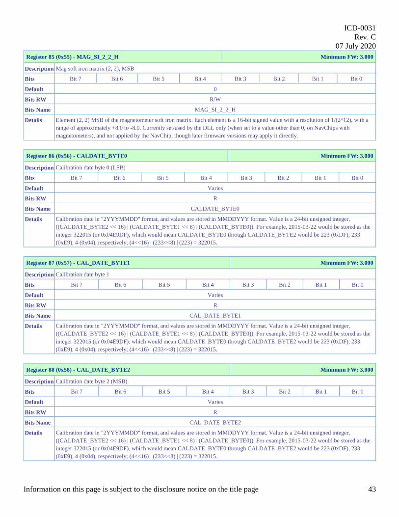
ICD-0031
Rev. C
07 July 2020
Information on this page is subject to the disclosure notice on the title page 43
Register 85 (0x55) - MAG_SI_2_2_H Minimum FW: 3.000
Description Mag soft iron matrix (2, 2), MSB
Bits Bit 7 Bit 6 Bit 5 Bit 4 Bit 3 Bit 2 Bit 1 Bit 0
Default 0
Bits RW R/W
Bits Name MAG_SI_2_2_H
Details Element (2, 2) MSB of the magnetometer soft iron matrix. Each element is a 16-bit signed value with a resolution of 1/(2^12), with a
range of approximately +8.0 to -8.0. Currently set/used by the DLL only (when set to a value other than 0, on NavChips with
magnetometers), and not applied by the NavChip, though later firmware versions may apply it directly.
Register 86 (0x56) - CALDATE_BYTE0 Minimum FW: 3.000
Description Calibration date byte 0 (LSB)
Bits Bit 7 Bit 6 Bit 5 Bit 4 Bit 3 Bit 2 Bit 1 Bit 0
Default Varies
Bits RW R
Bits Name CALDATE_BYTE0
Details Calibration date in "2YYYMMDD" format, and values are stored in MMDDYYY format. Value is a 24-bit unsigned integer,
((CALDATE_BYTE2 << 16) | (CALDATE_BYTE1 << 8) | (CALDATE_BYTE0)). For example, 2015-03-22 would be stored as the
integer 322015 (or 0x04E9DF), which would mean CALDATE_BYTE0 through CALDATE_BYTE2 would be 223 (0xDF), 233
(0xE9), 4 (0x04), respectively; (4<<16) | (233<<8) | (223) = 322015.
Register 87 (0x57) - CAL_DATE_BYTE1 Minimum FW: 3.000
Description Calibration date byte 1
Bits Bit 7 Bit 6 Bit 5 Bit 4 Bit 3 Bit 2 Bit 1 Bit 0
Default Varies
Bits RW R
Bits Name CAL_DATE_BYTE1
Details Calibration date in "2YYYMMDD" format, and values are stored in MMDDYYY format. Value is a 24-bit unsigned integer,
((CALDATE_BYTE2 << 16) | (CALDATE_BYTE1 << 8) | (CALDATE_BYTE0)). For example, 2015-03-22 would be stored as the
integer 322015 (or 0x04E9DF), which would mean CALDATE_BYTE0 through CALDATE_BYTE2 would be 223 (0xDF), 233
(0xE9), 4 (0x04), respectively; (4<<16) | (233<<8) | (223) = 322015.
Register 88 (0x58) - CAL_DATE_BYTE2 Minimum FW: 3.000
Description Calibration date byte 2 (MSB)
Bits Bit 7 Bit 6 Bit 5 Bit 4 Bit 3 Bit 2 Bit 1 Bit 0
Default Varies
Bits RW R
Bits Name CAL_DATE_BYTE2
Details Calibration date in "2YYYMMDD" format, and values are stored in MMDDYYY format. Value is a 24-bit unsigned integer,
((CALDATE_BYTE2 << 16) | (CALDATE_BYTE1 << 8) | (CALDATE_BYTE0)). For example, 2015-03-22 would be stored as the
integer 322015 (or 0x04E9DF), which would mean CALDATE_BYTE0 through CALDATE_BYTE2 would be 223 (0xDF), 233
(0xE9), 4 (0x04), respectively; (4<<16) | (233<<8) | (223) = 322015.
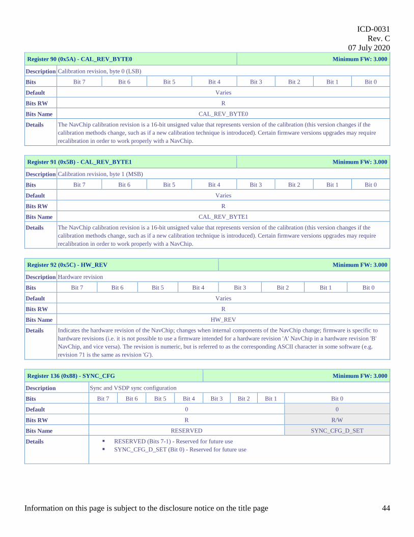
ICD-0031
Rev. C
07 July 2020
Information on this page is subject to the disclosure notice on the title page 44
Register 90 (0x5A) - CAL_REV_BYTE0 Minimum FW: 3.000
Description Calibration revision, byte 0 (LSB)
Bits Bit 7 Bit 6 Bit 5 Bit 4 Bit 3 Bit 2 Bit 1 Bit 0
Default Varies
Bits RW R
Bits Name CAL_REV_BYTE0
Details The NavChip calibration revision is a 16-bit unsigned value that represents version of the calibration (this version changes if the
calibration methods change, such as if a new calibration technique is introduced). Certain firmware versions upgrades may require
recalibration in order to work properly with a NavChip.
Register 91 (0x5B) - CAL_REV_BYTE1 Minimum FW: 3.000
Description Calibration revision, byte 1 (MSB)
Bits Bit 7 Bit 6 Bit 5 Bit 4 Bit 3 Bit 2 Bit 1 Bit 0
Default Varies
Bits RW R
Bits Name CAL_REV_BYTE1
Details The NavChip calibration revision is a 16-bit unsigned value that represents version of the calibration (this version changes if the
calibration methods change, such as if a new calibration technique is introduced). Certain firmware versions upgrades may require
recalibration in order to work properly with a NavChip.
Register 92 (0x5C) - HW_REV Minimum FW: 3.000
Description Hardware revision
Bits Bit 7 Bit 6 Bit 5 Bit 4 Bit 3 Bit 2 Bit 1 Bit 0
Default Varies
Bits RW R
Bits Name HW_REV
Details Indicates the hardware revision of the NavChip; changes when internal components of the NavChip change; firmware is specific to
hardware revisions (i.e. it is not possible to use a firmware intended for a hardware revision 'A' NavChip in a hardware revision 'B'
NavChip, and vice versa). The revision is numeric, but is referred to as the corresponding ASCII character in some software (e.g.
revision 71 is the same as revision 'G').
Register 136 (0x88) - SYNC_CFG Minimum FW: 3.000
Description Sync and VSDP sync configuration
Bits Bit 7 Bit 6 Bit 5 Bit 4 Bit 3 Bit 2 Bit 1 Bit 0
Default 0 0
Bits RW R R/W
Bits Name RESERVED SYNC_CFG_D_SET
Details RESERVED (Bits 7-1) - Reserved for future use
SYNC_CFG_D_SET (Bit 0) - Reserved for future use
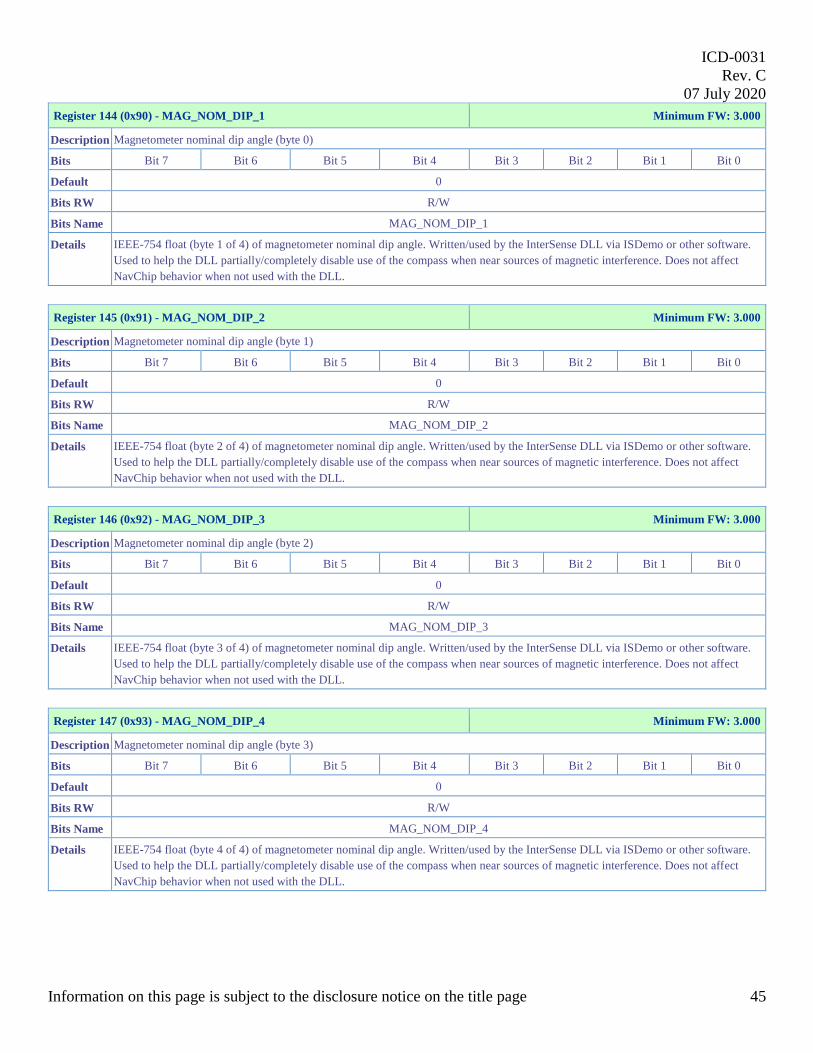
ICD-0031
Rev. C
07 July 2020
Information on this page is subject to the disclosure notice on the title page 45
Register 144 (0x90) - MAG_NOM_DIP_1 Minimum FW: 3.000
Description Magnetometer nominal dip angle (byte 0)
Bits Bit 7 Bit 6 Bit 5 Bit 4 Bit 3 Bit 2 Bit 1 Bit 0
Default 0
Bits RW R/W
Bits Name MAG_NOM_DIP_1
Details IEEE-754 float (byte 1 of 4) of magnetometer nominal dip angle. Written/used by the InterSense DLL via ISDemo or other software.
Used to help the DLL partially/completely disable use of the compass when near sources of magnetic interference. Does not affect
NavChip behavior when not used with the DLL.
Register 145 (0x91) - MAG_NOM_DIP_2 Minimum FW: 3.000
Description Magnetometer nominal dip angle (byte 1)
Bits Bit 7 Bit 6 Bit 5 Bit 4 Bit 3 Bit 2 Bit 1 Bit 0
Default 0
Bits RW R/W
Bits Name MAG_NOM_DIP_2
Details IEEE-754 float (byte 2 of 4) of magnetometer nominal dip angle. Written/used by the InterSense DLL via ISDemo or other software.
Used to help the DLL partially/completely disable use of the compass when near sources of magnetic interference. Does not affect
NavChip behavior when not used with the DLL.
Register 146 (0x92) - MAG_NOM_DIP_3 Minimum FW: 3.000
Description Magnetometer nominal dip angle (byte 2)
Bits Bit 7 Bit 6 Bit 5 Bit 4 Bit 3 Bit 2 Bit 1 Bit 0
Default 0
Bits RW R/W
Bits Name MAG_NOM_DIP_3
Details IEEE-754 float (byte 3 of 4) of magnetometer nominal dip angle. Written/used by the InterSense DLL via ISDemo or other software.
Used to help the DLL partially/completely disable use of the compass when near sources of magnetic interference. Does not affect
NavChip behavior when not used with the DLL.
Register 147 (0x93) - MAG_NOM_DIP_4 Minimum FW: 3.000
Description Magnetometer nominal dip angle (byte 3)
Bits Bit 7 Bit 6 Bit 5 Bit 4 Bit 3 Bit 2 Bit 1 Bit 0
Default 0
Bits RW R/W
Bits Name MAG_NOM_DIP_4
Details IEEE-754 float (byte 4 of 4) of magnetometer nominal dip angle. Written/used by the InterSense DLL via ISDemo or other software.
Used to help the DLL partially/completely disable use of the compass when near sources of magnetic interference. Does not affect
NavChip behavior when not used with the DLL.
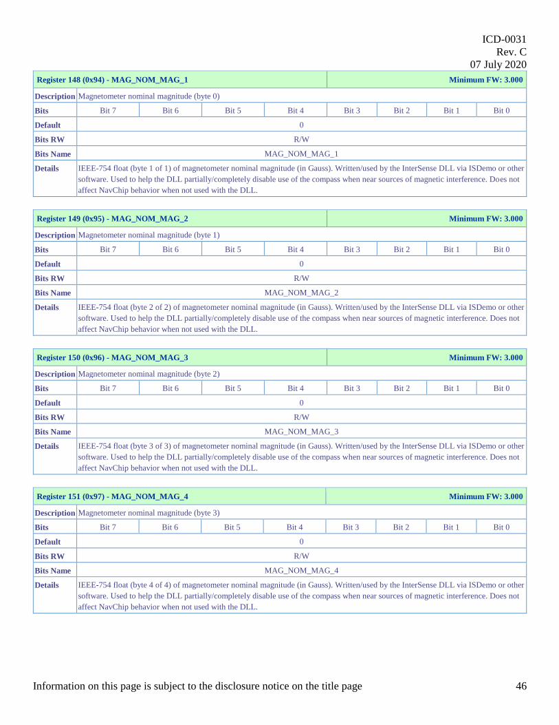
ICD-0031
Rev. C
07 July 2020
Information on this page is subject to the disclosure notice on the title page 46
Register 148 (0x94) - MAG_NOM_MAG_1 Minimum FW: 3.000
Description Magnetometer nominal magnitude (byte 0)
Bits Bit 7 Bit 6 Bit 5 Bit 4 Bit 3 Bit 2 Bit 1 Bit 0
Default 0
Bits RW R/W
Bits Name MAG_NOM_MAG_1
Details IEEE-754 float (byte 1 of 1) of magnetometer nominal magnitude (in Gauss). Written/used by the InterSense DLL via ISDemo or other
software. Used to help the DLL partially/completely disable use of the compass when near sources of magnetic interference. Does not
affect NavChip behavior when not used with the DLL.
Register 149 (0x95) - MAG_NOM_MAG_2 Minimum FW: 3.000
Description Magnetometer nominal magnitude (byte 1)
Bits Bit 7 Bit 6 Bit 5 Bit 4 Bit 3 Bit 2 Bit 1 Bit 0
Default 0
Bits RW R/W
Bits Name MAG_NOM_MAG_2
Details IEEE-754 float (byte 2 of 2) of magnetometer nominal magnitude (in Gauss). Written/used by the InterSense DLL via ISDemo or other
software. Used to help the DLL partially/completely disable use of the compass when near sources of magnetic interference. Does not
affect NavChip behavior when not used with the DLL.
Register 150 (0x96) - MAG_NOM_MAG_3 Minimum FW: 3.000
Description Magnetometer nominal magnitude (byte 2)
Bits Bit 7 Bit 6 Bit 5 Bit 4 Bit 3 Bit 2 Bit 1 Bit 0
Default 0
Bits RW R/W
Bits Name MAG_NOM_MAG_3
Details IEEE-754 float (byte 3 of 3) of magnetometer nominal magnitude (in Gauss). Written/used by the InterSense DLL via ISDemo or other
software. Used to help the DLL partially/completely disable use of the compass when near sources of magnetic interference. Does not
affect NavChip behavior when not used with the DLL.
Register 151 (0x97) - MAG_NOM_MAG_4 Minimum FW: 3.000
Description Magnetometer nominal magnitude (byte 3)
Bits Bit 7 Bit 6 Bit 5 Bit 4 Bit 3 Bit 2 Bit 1 Bit 0
Default 0
Bits RW R/W
Bits Name MAG_NOM_MAG_4
Details IEEE-754 float (byte 4 of 4) of magnetometer nominal magnitude (in Gauss). Written/used by the InterSense DLL via ISDemo or other
software. Used to help the DLL partially/completely disable use of the compass when near sources of magnetic interference. Does not
affect NavChip behavior when not used with the DLL.
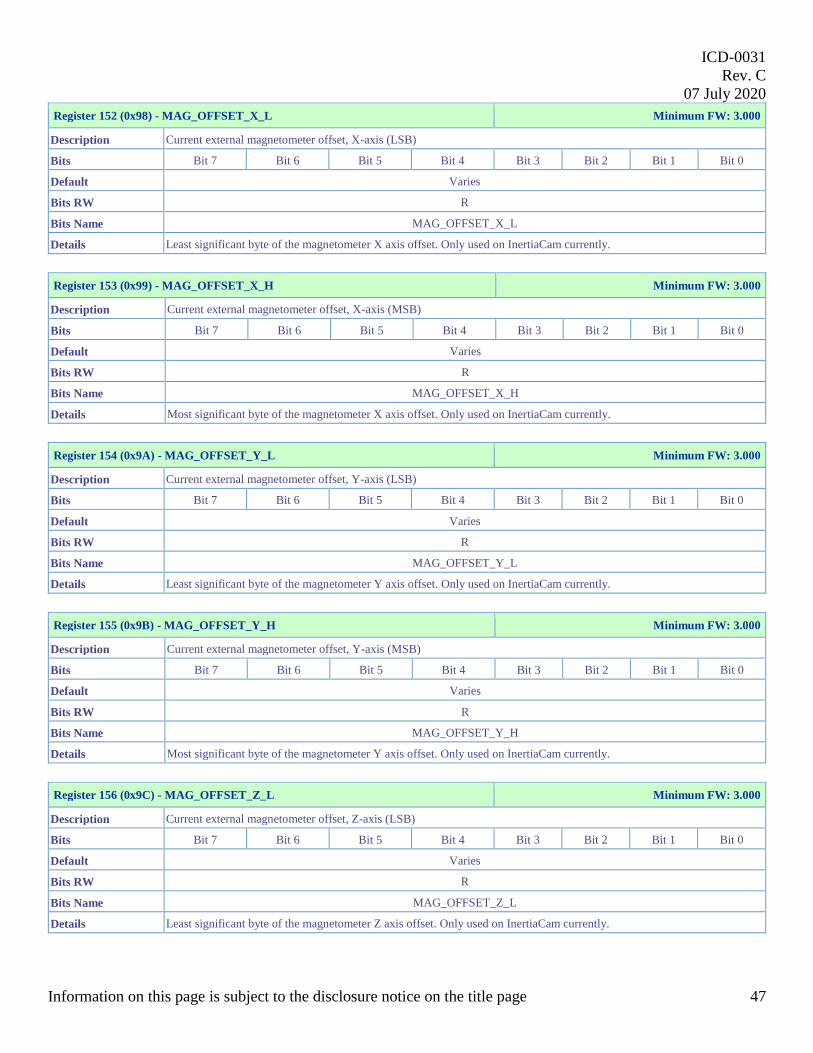
ICD-0031
Rev. C
07 July 2020
Information on this page is subject to the disclosure notice on the title page 47
Register 152 (0x98) - MAG_OFFSET_X_L Minimum FW: 3.000
Description Current external magnetometer offset, X-axis (LSB)
Bits Bit 7 Bit 6 Bit 5 Bit 4 Bit 3 Bit 2 Bit 1 Bit 0
Default Varies
Bits RW R
Bits Name MAG_OFFSET_X_L
Details Least significant byte of the magnetometer X axis offset. Only used on InertiaCam currently.
Register 153 (0x99) - MAG_OFFSET_X_H Minimum FW: 3.000
Description Current external magnetometer offset, X-axis (MSB)
Bits Bit 7 Bit 6 Bit 5 Bit 4 Bit 3 Bit 2 Bit 1 Bit 0
Default Varies
Bits RW R
Bits Name MAG_OFFSET_X_H
Details Most significant byte of the magnetometer X axis offset. Only used on InertiaCam currently.
Register 154 (0x9A) - MAG_OFFSET_Y_L Minimum FW: 3.000
Description Current external magnetometer offset, Y-axis (LSB)
Bits Bit 7 Bit 6 Bit 5 Bit 4 Bit 3 Bit 2 Bit 1 Bit 0
Default Varies
Bits RW R
Bits Name MAG_OFFSET_Y_L
Details Least significant byte of the magnetometer Y axis offset. Only used on InertiaCam currently.
Register 155 (0x9B) - MAG_OFFSET_Y_H Minimum FW: 3.000
Description Current external magnetometer offset, Y-axis (MSB)
Bits Bit 7 Bit 6 Bit 5 Bit 4 Bit 3 Bit 2 Bit 1 Bit 0
Default Varies
Bits RW R
Bits Name MAG_OFFSET_Y_H
Details Most significant byte of the magnetometer Y axis offset. Only used on InertiaCam currently.
Register 156 (0x9C) - MAG_OFFSET_Z_L Minimum FW: 3.000
Description Current external magnetometer offset, Z-axis (LSB)
Bits Bit 7 Bit 6 Bit 5 Bit 4 Bit 3 Bit 2 Bit 1 Bit 0
Default Varies
Bits RW R
Bits Name MAG_OFFSET_Z_L
Details Least significant byte of the magnetometer Z axis offset. Only used on InertiaCam currently.
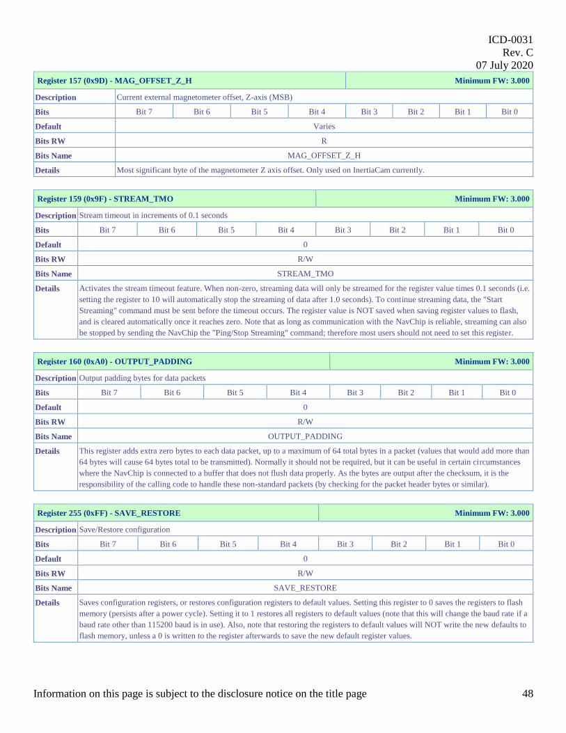
ICD-0031
Rev. C
07 July 2020
Information on this page is subject to the disclosure notice on the title page 48
Register 157 (0x9D) - MAG_OFFSET_Z_H Minimum FW: 3.000
Description Current external magnetometer offset, Z-axis (MSB)
Bits Bit 7 Bit 6 Bit 5 Bit 4 Bit 3 Bit 2 Bit 1 Bit 0
Default Varies
Bits RW R
Bits Name MAG_OFFSET_Z_H
Details Most significant byte of the magnetometer Z axis offset. Only used on InertiaCam currently.
Register 159 (0x9F) - STREAM_TMO Minimum FW: 3.000
Description Stream timeout in increments of 0.1 seconds
Bits Bit 7 Bit 6 Bit 5 Bit 4 Bit 3 Bit 2 Bit 1 Bit 0
Default 0
Bits RW R/W
Bits Name STREAM_TMO
Details Activates the stream timeout feature. When non-zero, streaming data will only be streamed for the register value times 0.1 seconds (i.e.
setting the register to 10 will automatically stop the streaming of data after 1.0 seconds). To continue streaming data, the "Start
Streaming" command must be sent before the timeout occurs. The register value is NOT saved when saving register values to flash,
and is cleared automatically once it reaches zero. Note that as long as communication with the NavChip is reliable, streaming can also
be stopped by sending the NavChip the "Ping/Stop Streaming" command; therefore most users should not need to set this register.
Register 160 (0xA0) - OUTPUT_PADDING Minimum FW: 3.000
Description Output padding bytes for data packets
Bits Bit 7 Bit 6 Bit 5 Bit 4 Bit 3 Bit 2 Bit 1 Bit 0
Default 0
Bits RW R/W
Bits Name OUTPUT_PADDING
Details This register adds extra zero bytes to each data packet, up to a maximum of 64 total bytes in a packet (values that would add more than
64 bytes will cause 64 bytes total to be transmitted). Normally it should not be required, but it can be useful in certain circumstances
where the NavChip is connected to a buffer that does not flush data properly. As the bytes are output after the checksum, it is the
responsibility of the calling code to handle these non-standard packets (by checking for the packet header bytes or similar).
Register 255 (0xFF) - SAVE_RESTORE Minimum FW: 3.000
Description Save/Restore configuration
Bits Bit 7 Bit 6 Bit 5 Bit 4 Bit 3 Bit 2 Bit 1 Bit 0
Default 0
Bits RW R/W
Bits Name SAVE_RESTORE
Details Saves configuration registers, or restores configuration registers to default values. Setting this register to 0 saves the registers to flash
memory (persists after a power cycle). Setting it to 1 restores all registers to default values (note that this will change the baud rate if a
baud rate other than 115200 baud is in use). Also, note that restoring the registers to default values will NOT write the new defaults to
flash memory, unless a 0 is written to the register afterwards to save the new default register values.