nbsir 76-846 nbs phase noise measurement system
TRANSCRIPT
NBSIR 76-846
AN NBS PHASE NOISE MEASUREMENT SYSTEM
BUILT FOR FREQUENCY DOMAIN MEASUREMENTS
ASSOCIATED WITH THE GLOBAL POSITIONING SYSTEM
S.R. Stein
Time and Frequency Division
Institute for Basic Standards
National Bureau of Standards
Boulder , Colorado 80302
August 1976

NBSIR 76-846
AN NBS PHASE NOISE MEASUREMENT SYSTEM
BUILT FOR FREQUENCY DOMAIN MEASUREMENTS
ASSOCIATED WITH THE GLOBAL POSITIONING SYSTEM
S.R. Stem
Time and Frequency Division
Institute for Basic Standards
National Bureau of Standards
Boulder, Colorado 80302
August 1976
U.S. DEPARTMENT OF COMMERCE, Elliot L. Richardson, Secretary
Edward 0. Vetter, Under Secretary
Dr. Betsy Ancker-Johnson , Assistant Secretary for Science and Technology
NATIONAL BUREAU OF STANDARDS, Ernest Ambler, Acting Director
AN NBS PHASE NOISE MEASUREMENT SYSTEM
BUILT FOR FREQUENCY DOMAIN MEASUREMENTS
ASSOCIATED WITH THE GLOBAL POSITIONING SYSTEM
S.R. Stein
ABSTRACT
A self-contained system is described which was constructed to perform phase noise
measurements for the first phase of the Global Positioning System (GPS). It is capable
of evaluating a pair of similar oscillators or a single oscillator and a frequency syn-
thesizer using the phase-lock technique. Three features have been included to simplify
the operation of the instrument: internal circuitry automatically detects an out-of-lock
condition; an optimized second order phase-lock loop reduces phase error by a factor of5
10 over a first order loop; selection of operating mode is made by a single front Danel
switch
.
KEY WORDS: Phase-locked loop, phase noise measurement system, spectral density
of phase, Global Positioning System.
I. INTRODUCTION
A phase noise measurement system (NBS-PNMS) has been designed and constructed which
permits the measurement of the spectral density of phase fluctuations S.(f) of a pair of
a pair of (10.23 MHz) oscillators. The basic principles of operation are discussed in Sections
I and II. Section III describes the recommended operating procedure. Section IV discusses
the interpretation of measurements and Section V gives actual noise floor measurements for
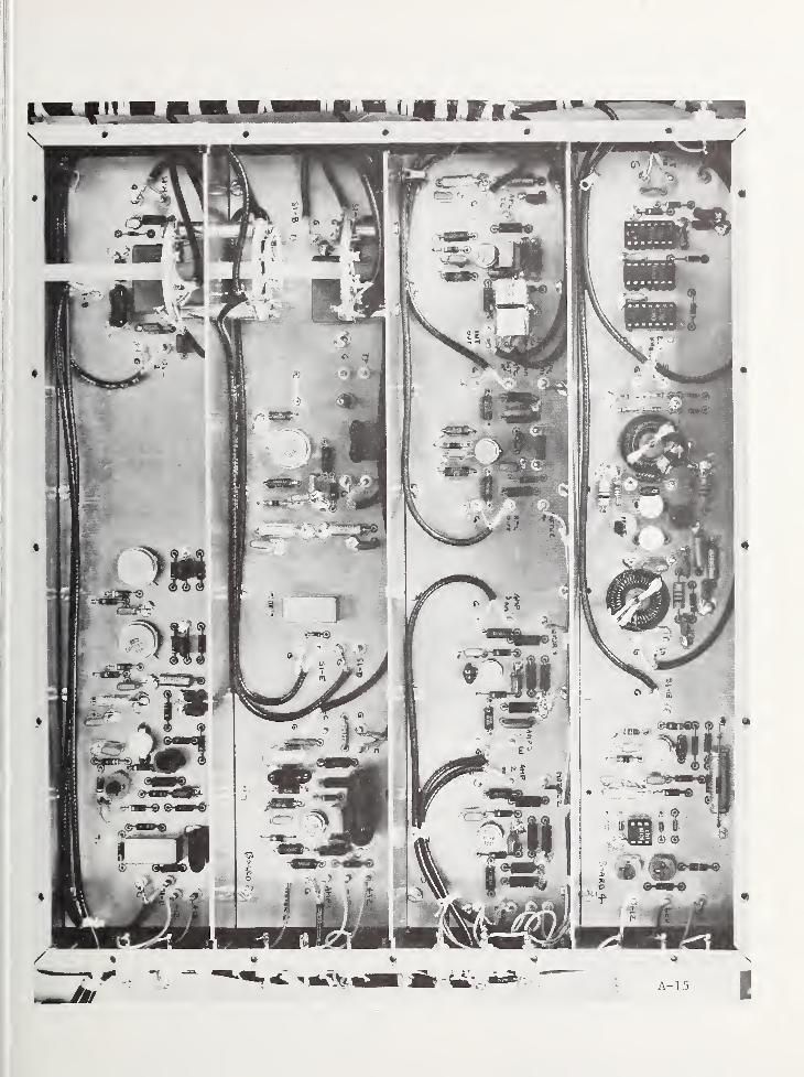
relatively low signal levels. The Appendix contains photographs of the instrument and the
detailed circuit diagrams.
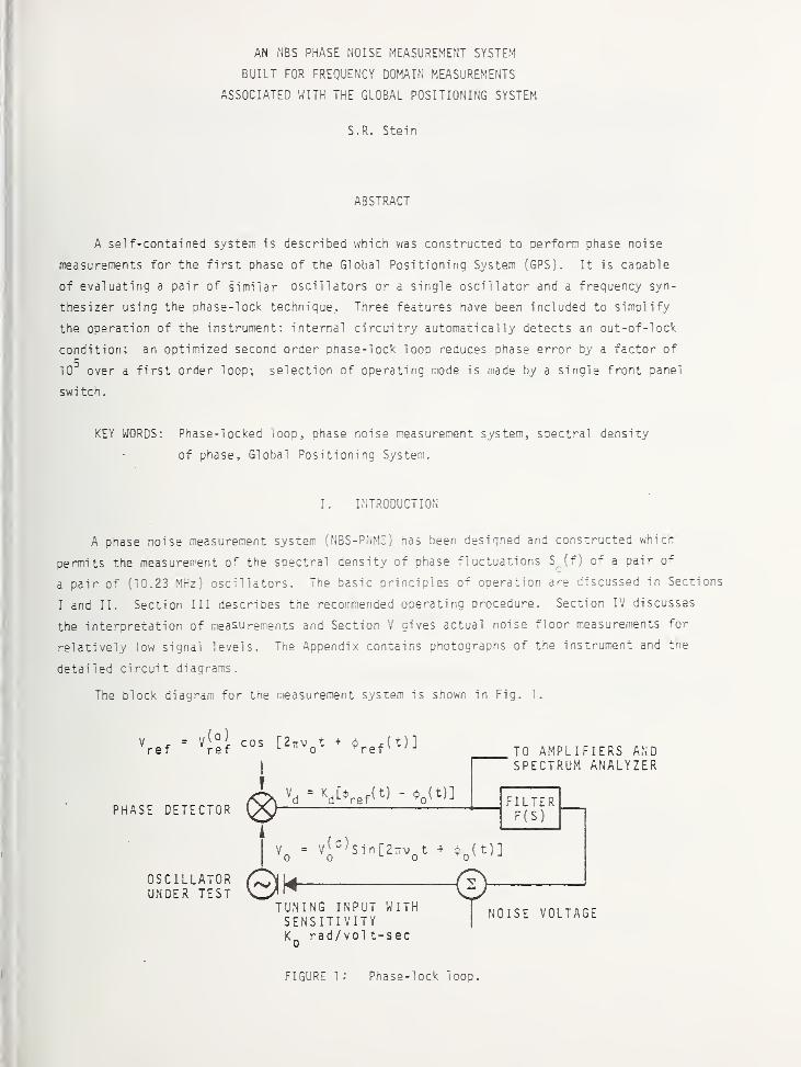
The block diagram for the measurement system is shown in Fig. 1.
Vref
Vref
" s t 2'V +^ref'
1^
)PHASE DETECTOR
Vd
- Kd[*ref
(t) - »0(t)]
TO AMPLIFIERS ANDSPECTRUM ANALYZER
FILTERF(S)
= vi0) Sin[2™ t + * ft
(t)]
OSCILLATORUNDER TEST 0*
TUNING INPUT WITHSENSITIVITYK rad/volt-sec
NOISE VOLTAGE
FIGURE 1 : Phase-lock loop.
The noise voltage summed into the loop is a schematic way of representing <j> (t)', the open
loop phase noise of the oscillator under test. Phase noise in the reference oscillator is
contained in the 4g-(t) term. This is the general block diagram for any phase-lock loop [1],
The purpose of using a phase-lock loop is simply to guarantee that the two oscillators
are on the average in phase quadrature. This condition is indicated by the sine and
cosine outputs of the two oscillators. When the oscillators are near quadrature the
voltage output of the phase detector is proportional to the difference in phase between
the two output signals.
Analysis of the phase-lock loop yields the result [2]
eq ' Vef v
G (s'eq
1 + Geq
(1)
where G (s) is the open-loop transfer function defined by
G (seq
K K, F (s)_ o d
v '
(2)
and 4n
(s) and A ^ (s) are the Laplace transforms of the corresponding time varying
quantities. We can also calculate the voltage output of the phase detector.
Vd(s)
Kd Kef (s) - +
1 + S fs)(3)
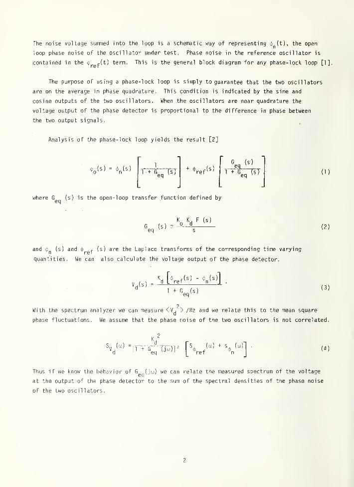
With the spectrum analyzer we can measure <V. > /Hz and we relate this to the mean square
phase fluctuations. We assume that the phase noise of the two oscillators is not correlated.
2
'
1
(4)Su
(co)vdm£w [\ef
("> + •>>]
Thus if we know the behavior of G (jto) we can relate the measured spectrum of the voltage
at the output of the phase detector to the sum of the spectral densities of the phase noise
of the two oscillators.
2
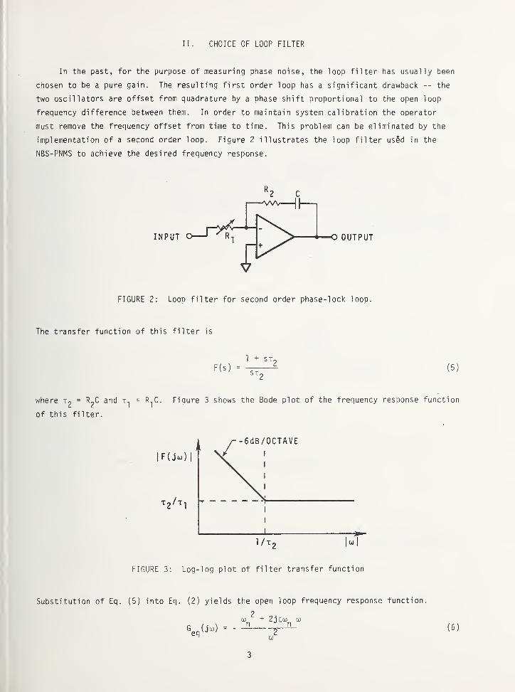
II. CHOICE OF LOOP FILTER
In the past, for the purpose of measuring phase noise, the loop filter has usually been
chosen to be a pure gain. The resulting first order loop has a significant drawback -- the
two oscillators are offset from quadrature by a phase shift proportional to the open loop
frequency difference between them. In order to maintain system calibration the operator
must remove the frequency offset from time to time. This problem can be eliminated by the
implementation of a second order loop. Figure 2 illustrates the loop filter used in the
NBS-PNMS to achieve the desired frequency response.
The transfer function of this filter is
where = R^C and t.| = R-jC. Figure 3 shows the Bode plot of the frequency response function
of this filter.
INPUT
V
FIGURE 2: Loop filter for second order phase-lock loop.
-6dB/0CTAVE
FIGURE 3: Log-log plot of filter transfer function
Substitution of Eq. (5) into Eq. (2) yields the open loop frequency response function.
2,
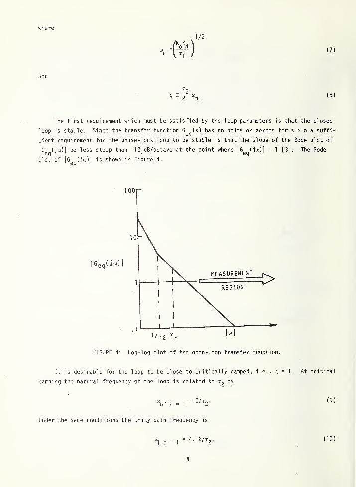
where
1/2
/o Kd \
(7)
and
The first requirement, which must be satisfied by the loop parameters is that .the closed
loop is stable. Since the transfer function Gg^(s) has no poles or zeroes for s > o a suffi-
cient requirement for the phase-lock loop to be stable is that the slope of the Bode plot of
|
G
g( joj) |
be less steep than -12 dB/octave at the point where |Geq(ju>)| = 1 [3]. The Bode
plot of (Geq(joj)| is shown in Figure 4.
G eq ( jw)
|
1/T2
FIGURE 4: Log-log plot of the open-loop transfer function.
It is desirable for the loop to be close to critically damped, i.e., 5 = 1 . At critical
damping the natural frequency of the loop is related to by
V c = 1
= 2/T 2- (9)
Under the same conditions the unity gain frequency is
"1,5 = 1
= 4J2/T 2' (10)
4
The second requirement which must be satisfied by the phase-lock loop relates to the
accuracy with which spectral density measurements may be made. Substitution of Eq. (6)
into Eq. (4) yields
K2 . A
d S. (u>) + S. (w)$ref *n
(ID
Since the proportionality factor has a high pass response, it is possible to use an essentially
constant calibration to relate Sy (co) and S (id). We require that
svd
(w) = Kd
2S. (u>) + S. (co)
*ref *n
(12)
with no more than 10% error for all Fourier frequencies greater than 27Trad/sec. For the
critically damped loop this reduces to a requirement on t^:
> 1.4 seconds
.
The NBS-PNMS has t„ = 12 seconds.
The third requirement on loop performance is that frequency offset between the two
oscillators produces negligible phase shift of the oscillators away from quadrature. In
the ideal loop the phase error for a frequency error Av introduced at time t = o is
'error
-oi t
= 2^Avt en
(13)
In the actual circuit there is a finite phase error due to the limited loop gain of the
5amplifier of Fig. 2. In the NBS-PNMS the phase error is reduced by 10 compared to its
value for a first order loop. Typically the error is less than the residual phase error
due to the voltage offset at the mixer output and should be much less than one degree.
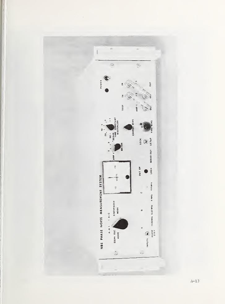
III. OPERATION
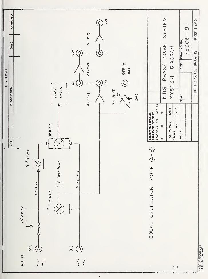
There are two modes of operation which permit either the comparison of two (equal)
oscillators at 10.23 MHz or the comparison of a single 10.23-MHz oscillator with a 5-MHz
oscillator and a synthesizer. The operating mode is selected by a single front panel
switch.
Equal oscillator mode
Turn the instrument on.
5
In this mode the total phase noise from two 10.23 MHz oscillators may be measured.
The two oscillators are connected to inputs A and B. The input voltage (7 dBm nominal)
should be as large as possible but the input current should not exceed 40 mA peak. The
beat between the two oscillators may be observed at the amplifier 1 output or, if it is
sufficiently slow, on the meter with the meter switch in position AMP 1. The out-of-lock
1 ight shoul d be on
.
With the Set Up-Lock switch in the Set Up position the varactor input of one oscillator
should be connected to the servo-output connector. Before making this connection check to
see if the polarity of the dc bias voltage is appropriate for the oscillator to be controlled
If necessary, it may be changed by throwing the SPDT switch mounted on the right side at the
front of the interior shield box. The varactor input of the other oscillator should be
grounded. Now the time constant switch should be set to minimum and the coarse and fine
bias controls adjusted to obtain a beat-period of approximately 10 seconds. Close the
Set Up-Lock switch and observe whether the beat disappears and the out-of-lock light goes
out. If phase-lock is not achieved with the time constant switch set to minimum, open the
loop and readjust the beat period to longer than 10 sec. Then repeat the above procedure.
When the loop is locked turn the time constant switch CCW to achieve the desired loop
response.
If the required slow beat frequencies are not obtained it may be necessary to (1) feed-
back to the other oscillator or (2) apply a bias voltage to the oscillator which is not in
the phase-lock loop.
Before making any phase noise measurements it is necessary to determine if the time
constant of the loop has the proper value, i.e., if the loop is near critically damping.
This is done by measuring the step response of the loop which should be an exponential
decay with a 1/e time constant of approximately 3 seconds. The step response of the loop
may be measured with the following procedure: Connect the output of amplifier #1 to a
strip chart recorder or an oscilloscope. With the loop locked and the strip chart recorder
running a nominal 10° phase step is introduced by throwing the phase-step switch. The
response of the loop is observed on the recorder. It should have the form of a single
exponential decay with 3 second time constant and not more than ^10% overshot.
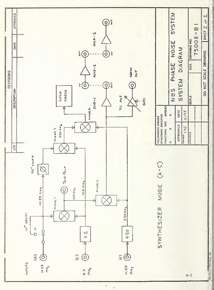
Synthesizer mode
Operation in this mode is essentially the same as in the equal oscillator mode. Only
the differences are described here.
A 10.23-MHz oscillator is connected to input A; a 5-MHz oscillator and a synthesizer are
connected to the appropriate inputs (C). The servo output is connected to the varactor
input of the 10.23-MHz oscillator. The set up procedure is the same except that the initial
10 second beat period is obtained by adjusting the synthesizer frequency near 11.5 MHz.
6
IV. PHASE NOISE MEASUREMENT TECHNIQUE
In Section II we established that there is a simple relationship between the spectral
density of the voltage fluctuations at the output of the phase detector and the spectral
density of the total phase fluctuations in the oscillators under test. We now denote the
total phase spectral density by S,(f):
Y Vef Tn
From Eq. (12) we then obtain
sv
(f)
y f> ~- -jj- (is)
where Kd
is the sensitivity of the phase detector in volts/rad. There is one measurement
amplifier (no. 1) permanently connected to the phase detector and two additional amplifiers
which may be connected in series via their front panel jacks. At the output of amplifier #1
S (f)
y f>
~-
ncj"2 ^
where K-| is the phase sensitivity at the output of amplifier no. 1 and is equal to gain of
amp 1 x K^. If amplfiers 2 and/or 3 are used to make the measurements the additional gain
is taken into account in the following manner
S ff)SV(f)
(17)
WTiere A is the total gain following amplifier #1 -
The spectral density of the output voltage, S^(f), is measured with a wave analyzer. With
such an instrument one measures the rms voltage, V , in some known bandwidth. Under thea rmsassumption that the spectral density varies slowly within the bandwidth, B, of the wave
analyzer it may be estimated to be
S..(f ) = V2 /B • (18.)
V ' rms v'
The final formula for S,(f) is
The measured spectral density of phase combines the phase noise from all the oscillators
involved in the measurement. However, sometimes prior knowledge is available which permits
further interpretation of the data. In the equal oscillator mode the two oscillators under
test often have identical design and construction and are therefore assumed to contribute
equally to the measured noise. In this case
S (f, one oscillator) = \ S.(f) (20)<j> 2 <f>
The phase noise measured using the synthesizer mode is interpreted as the noise of the single
oscillator under test. In this case
S^(f, one oscillator) = S,(f)
All such interpretations are subject to the restriction that S (f) exceeds the measured
noise of the NBS-PNMS by 6 dB.*
Cal ibration
Amplifiers 2 and 3 each have a nominal gain of 10 and bandwidth of 40 KHz. The only
calibration of the NBS-PNMS which must be performed -for each measurement set-up is , the
phase sensitivity at the output of amplifier #1 . The phase sensitivity is constant to 1 dB
up to 10 KHz. The recommended technique for measuring K^ is summarized below:
With the phase-lock loop open record the beat (output of amplifier #1) between the two
oscillators on a strip chart recorder. If necessary change only the bias voltage to obtain
a sufficiently short beat period (approximately 10 sec). The distance between adjacent
zero crossings on the chart determines tt rad and the slope of the line near the zero crossing
is K.| in volts/rad. It is important to use only the region within t tt/6 of the zero crossing
in order to limit to 5% the error due to the fact that sine 4> f <j>.
Two other methods may be used to determine K^ but they have large probability of
systematic error and are therefore not recommended for precise measurements. The first
of these methods is to measure \'p^.p» the peak-to-peak amplitude of beat between the two
oscillators at the output of amplifier #1 divided by the input phase shift is K^ . Reflec-
tions from the phase detector cause this technique to suffer systematic errors.
*In the past the quantity J (f) has been used to describe the phase noise of an individual
device, a" (f ) was defined as the ratio of the power per hertz bandwidth in one phase noise
sideband offset a frequency f from the carrier to the total signal power. For \§ > << 1
J (f) = i S If, one oscillator).2 d>
8
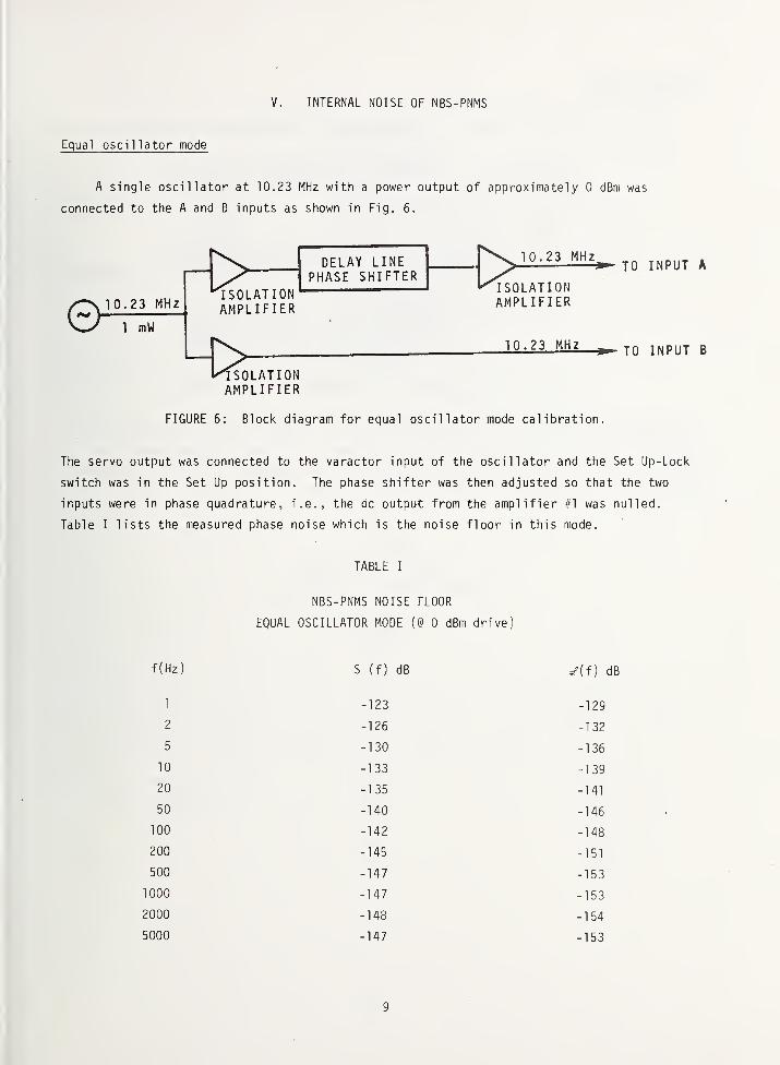
V. INTERNAL NOISE OF NBS-PNMS
Equal oscillator mode
A single oscillator at 10.23 MHz with a power output of approximately 0 dBm was
connected to the A and B inputs as shown in Fig. 6.
© 10.23 MHz
1 mW
DELAY LINE>
PHASE SHIFTER
10.23 MHzTO INPUT A
AMPLIFIER
ISOLATIONAMPLIFIER
^^0
10.23 MHz m TQ INp|JT B
ISOLATIONAMPLIFIER
FIGURE 6: Block diagram for equal oscillator mode calibration.
The servo output was connected to the varactor input of the oscillator and the Set Up-Lock
switch was in the Set Up position. The phase shifter was then adjusted so that the two
inputs were in phase quadrature, i.e., the dc output from the amplifier #1 was nulled.
Table I lists the measured phase noise which is the noise floor in this mode.
TABLE I
NBS-PNMS NOISE FLOOR
EQUAL OSCILLATOR MODE (@ 0 dBm drive)
f(Hz!
1
2
5
10
20
50
100
200
500
1000
2000
5000
S (f) dB
-123
-126
-130
-133
-135
-140
-142
-145
-147
-147
-148
-147
^(f) dB
-129
-132
-136
-139
-141
-146
-148
-151
-153
-153
-154
-153
9
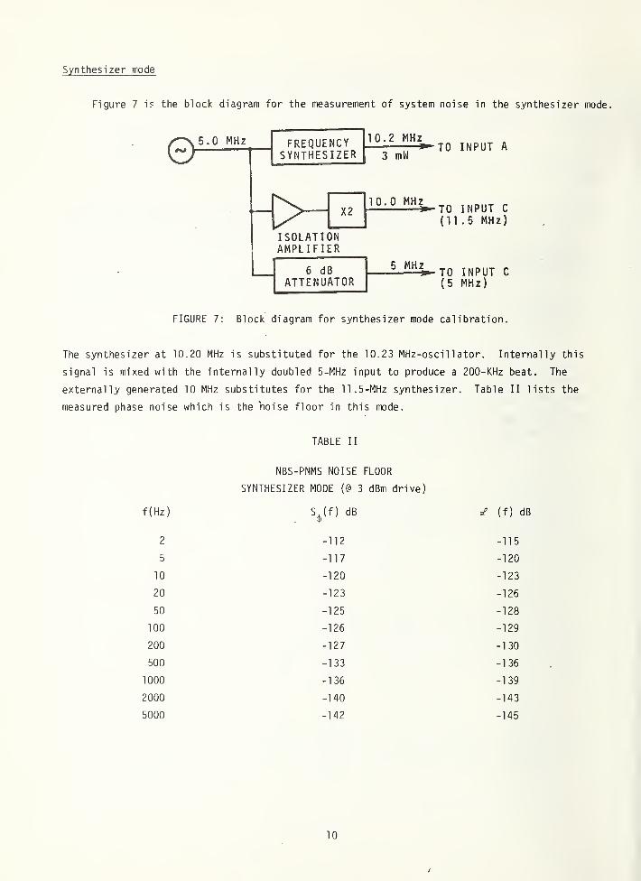
Synthesizer mode
Figure 7 is the block diagram for the measurement of system noise in the synthesizer mode.
© 5.0 MHz FREQUENCYSYNTHESIZER
X2
ISOLATIONAMPLIFIER
6 dBATTENUATOR
10.2 MHz
3 mW
10.0 MHz
5 MHz
TO INPUT A
TO INPUT C
(11.5 MHz)
TO INPUT C
(5 MHz)
FIGURE 7: Block diagram for synthesizer mode calibration.
The synthesizer at 10.20 MHz is substituted for the 10.23 MHz-oscillator. Internally this
signal is mixed with the internally doubled 5-MHz input to produce a 200-KHz beat. The
externally generated 10 MHz substitutes for the 11.5-MHz synthesizer. Table II lists the
measured phase noise which is the noise floor in this mode.
TABLE II
f(HZ;
NBS-PNMS NOISE FLOOR
SYNTHESIZER MODE (P 3 dBm drivel
SAf) dB J (f) dB
2
5
10
20
50
100
200
500
1000
2000
5000
-112
-117
-120
-123
-125
-126
-127
-133
-136
-140
-142
-115
-120
-123
-126
-128
-129
-130
-136
-139
-143
-145
10
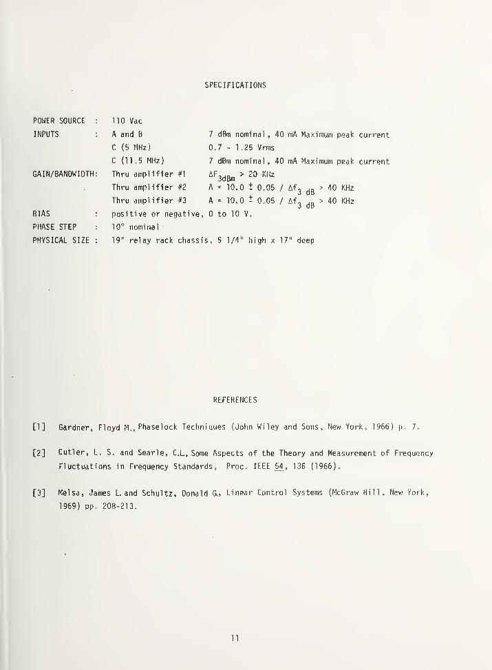
SPECIFICATIONS
POWER SOURCE
INPUTS
GAIN/BANDWIDTH:
BIAS
PHASE STEP
PHYSICAL SIZE
110 Vac
A and B
C (5 MHz)
C (11,5 MHz
)
Thru amplifier #1
Thru amplifier #2
Thru amplifier #3
positive or negative, 0 to 10 V.
10° nominal
19" relay rack chassis, 5 1/4" high x 17" deep
7 dBm nominal , 40 niA Maximum peak current
0.7 - 1 .25 Vrms
7 dBm nominal, 40 mA Maximum peak current
AF„ Jn_ > 20 KHz
40 KHz
3dBmA = 10.0 t 0.05 / Af
A = 10.03 dB
0.05 / Af 0 > 40 KHz3 dB
REFERENCES
[1] Gardner, Floyd M., Phaselock Techniques (John Wiley and Sons, New York, 1966) p. 7.
[2] Cutler, L. S. and Searle, C.L, Some Aspects of the Theory and Measurement of Frequency
Fluctuations in Frequency Standards, Proc. IEEE 54, 136 (1966).
[3] Melsa, James L and Schultz, Donald G., Linear Control Systems (McGraw Hill, New York,
1969) pp. 208-213.


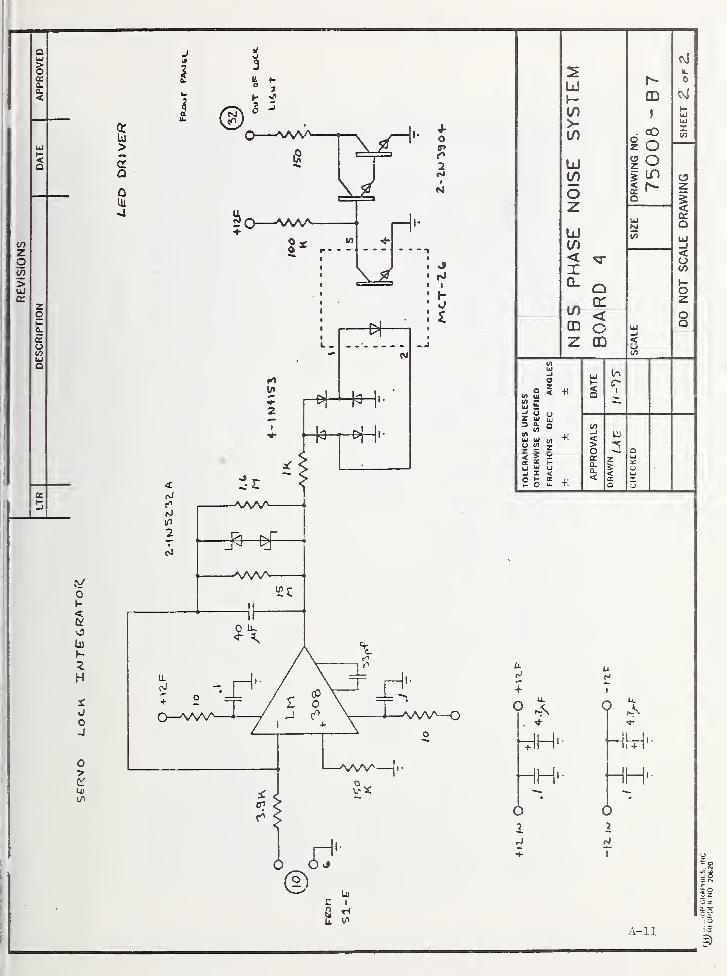
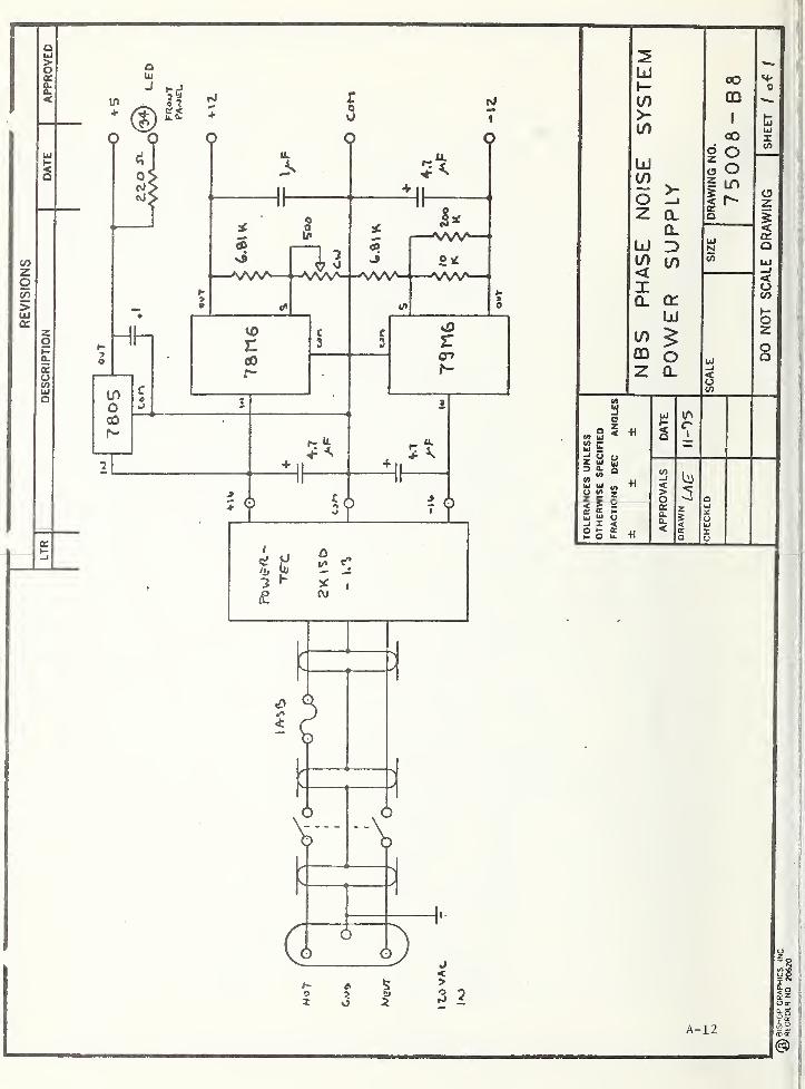
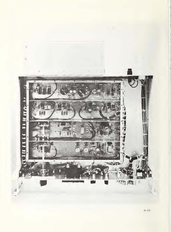
APPENDIX
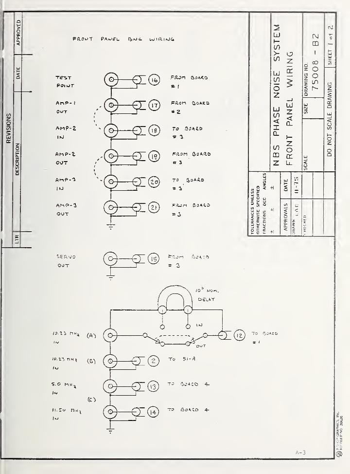
<
tozgco
>
poiur
AnP- I
Oct
AmP-2IkJ
AhP-10\JT
IO
Out
'-0—gr©
u 3
3
Ucn>- o10
u
oz
uC/l
<Q_
z
LxJ
z<CL
\—
zo
Z Ll
CD
cO
ooLT)
Q
Z lj
3 0.
U kJ
CJ (/}
< ISi2 5
z
<crQ
<OCO
OQ
OOT£1
* 3
SO MH^
<i.S"o riM:
0—^T©-QI©
-v^-Ql© To Cjacd
To Sl-fl
to 6ja:o 4-
T£> do A CD 4-
A-3
>oKa.a.
<
V)zgen
>LUq:
©15<31-A
zc
a.
U
©3?si
To
tt7_
- ©Sl-C
* 1©33
S WD
To r^jAZr>
€L©10.00 r*i
a©
To Go a ~_r>
2.
z
2ui—LO>-
LO
uCO
5 §zi
Id ULO H-
Q_
LO
CD
LO
l_d
QO
Dto u
_J x
nm
i Oa o
<
<
OQ
A-
5


>occa.a.<
cnzgCO
>LlI
cczc
crotoUJ
0
o
H
joj
o
Lu
I—I/)
>
UJ
O
u<IQ_
1/1
mcr<cCD
Ifl UJv> jr
z a a= ft
sMUJ Ul (flU <S> 2
K * hUi UJ u—i X <
zi
CD
I
. cO
i og os in
cvj
0
z
<Q
<oCO
OQ
a.
o A
HHHH'
6
u
9 :s
HH"
HH"62
i
38
li3i
A-ll
>o5S
k
s
COzOCO
>
oCOUJa
5UJI-t/)
>-
</)
UJ(/)
o ^Z Q_
CL
U 3^ t/)<tIOL a:
UJ
£D oZ CL
ovi u
J O oZ u u= 9z a
til u mo in S
<1 2K S Hu bi (j-J X <o h aO u.
< -H
oo
CD
I
oO
oO
OZ
Q<
UJ
y aUJ_i<oCO
1-ozo
UJ Q<oCO
A-12
(§>
A- 13
A-14
NBS-1 14A (REV. 7-73)
U.S. DEPT. OF COMM.BIBLIOGRAPHIC DATA
SHEET
1. PUBLIC A 1 ION OR REPORT NO.
NBSIR 76-846
2. Gov't AccessionNo.
3. Recipient's Accession No.
4. TITLE AND SUBTITLE
AN NBS PHASE NOISE MEASUREMENT SYSTEM BUILT FOR
FREQUENCY DOMAIN MEASUREMENTS ASSOCIATED WITH THEGLOBAL POSITIONING SYSTEM
5. Puhl i< at ion Date
August 19766. Performing Organization ('ode
?77 04
7. AUTHOR(S)
S. R. STEIN8. Performing Organ. Report No.
9. PERFORMING ORGANIZATION NAME AND ADDRESS
NATIONAL BUREAU OF STANDARDSDEPARTMENT OF COMMERCEWASHINGTON, D.C. 20234
10. Project/Task/Work Unit No.
11. < onlrac I Cirani No.
Contract #SMST0050
12. Sponsoring Organization Name and Complete Address (Street, City, State, ZIP) 13. 1 ype of Report & Period( (iv ered
14. Sponsoring Agenc y ( ode
15. SUPPLEMENTARY NOTES
16. ABSTRACT (A 200-word or less factual summary of most significant information. If document includes a significant
bibliography or literature survey, mention it here.)
A self-contained system is described which was constructed to performphase noise measurements for the first phase of the Global PositioningSystem (GPS). It is capable of evaluating a pair of similar oscillatorsor a single oscillator and a frequency synthesizer using the phase-locktechnique. Three features have been included to simplify the operation ofthe instrument: internal circuitry automatically detects an out-of-lockcondition; an optimized second order phase-lock loop reduces phase error by a
factor of 10^ over a first order loop; selection of operating mode is madeby a single front panel switch.
17. KEY WORDS (six to twelve entries; alphabetical order; capitalize only the first letter of the first key word unless a proper
name; separated by semicolons
)
Phase-locked loop, phase noise measurement system, spectral density of phase,
18. AVAILABILITY Unlimited 19. SECURITY CLASS(THIS REPORT)
21. NO. OF PAGES
|For Official Distribution. Do Not Release to NTIS
UNCLASSIFIED 29
_' Order From Sup. of Doc, U.S. Government Printing OfficeWashington. D.C. 20402. SD Cat. No. C13
20. SECURITY CLASS(THIS PAGE)
22. Price
P^? Order From National Technical Information Service (NTIS)Springfield, Virginia 22151 UNCLASSIFIED $4.00
USCOMM-DC 29042-P74