nbti-aware synthesis of digital circuits synthesis of digital circuits sanjay kumar chris kim sachin...
TRANSCRIPT

NBTI-Aware Synthesis
of Digital Circuits
Sanjay Kumar
Chris Kim
Sachin Sapatnekar
University of Minnesota
DAC 2007 – Session 20.3

2
Negative Bias Temperature Instability (NBTI)
Vdd
G
S
0
-Vdd
Vdd
0
VG = 0 VG = Vdd
SiH + h+ → Si+ + ½H2
Si H
Si H
Si H
H2
Substrate PolyOxide
VG = 0 VS = Vdd
D
VB
VD
B
G
oxide S
Stress Relaxation
Increase in PMOS Vth gradually over a few years
3
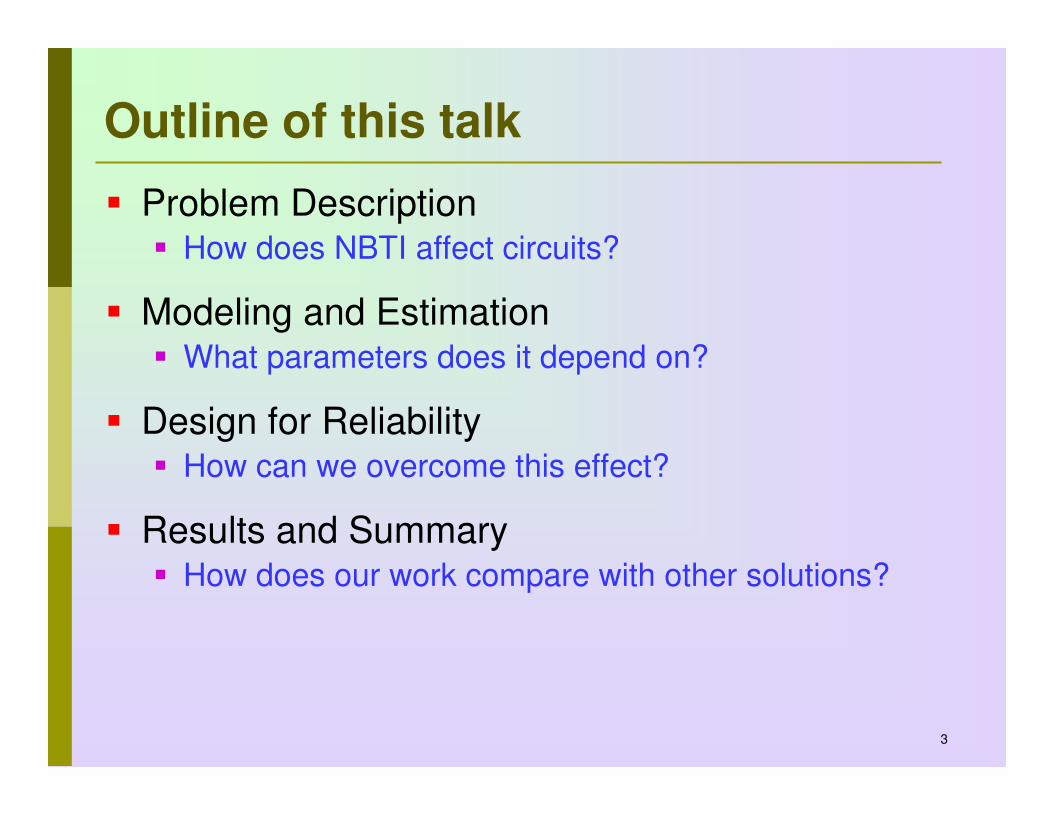
Outline of this talk
� Problem Description� How does NBTI affect circuits?
� Modeling and Estimation� What parameters does it depend on?
� Design for Reliability� How can we overcome this effect?
� Results and Summary� How does our work compare with other solutions?

4
Problem Statement
NBTI in PMOS devices
Aging - circuits become slower
Operate circuits at lower speeds
NBTI-aware robust circuit design
Design NBTI-resilient circuits with the least amount of overhead

5
Sizing for Reliability [DATE06, ICCD06, ISQED07]
Design sized accounting for aging
Still meets specs
Area overheadArea overhead Reliable designReliable design
Original design Gates become weak,target freq not met
After 10 years
After 10 years

6
“Worst Case” NBTI Assumption
� Worst case NBTI� All PMOS devices degrade
maximally
� Easy to estimate impact
� Conservative and pessimistic
� Actual Circuit Operation� NBTI effect based on Signal
Probability (SP)
� Each node has a certain SP
� Worst case can never happen
1
1
1
1
1
1
11
1
0.5
0.5
0.5
0.5
0.5
0.25
0.250.375
0.375

7
Limitations of Sizing based flow
Allows changes in gate sizes only
Synthesize circuits accounting for NBTI-induced delay degradation.
Nominal Timing
Spec = T0 ps.
10 years aging
10% delay increase
New Timing Spec
= 0.91T0 ps.
Sizing

8
Our Work
� Focus
� Incorporate NBTI-guard banding into synthesis during tech-mapping
� Reduce pessimism in estimation of aging effects
� Design best NBTI tolerant structures
� Requirements
� NBTI-aware library characterization
� Signal probability of primary inputs
� Suitable cost function (delay, area, power, etc) in tech-mapping
NBTI Modeling and Library Characterization
Key Results
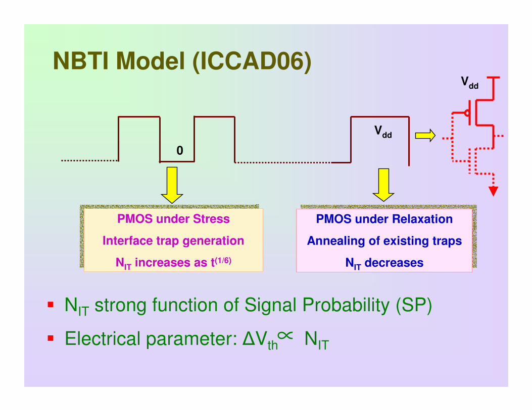
NBTI Model (ICCAD06)
� NIT strong function of Signal Probability (SP)
� Electrical parameter: ∆Vth NIT
Vdd
PMOS under Stress
Interface trap generation
NIT increases as t(1/6)
PMOS under Stress
Interface trap generation
NIT increases as t(1/6)
PMOS under Relaxation
Annealing of existing traps
NIT decreases
PMOS under Relaxation
Annealing of existing traps
NIT decreases
∝
0
Vdd

Vth Degradation
0.35
0.37
0.39
0.41
0.43
0.45
0.47
0 0.1 0.2 0.3 0.4 0.5 0.6 0.7 0.8 0.9 1
Signal Probability (SP)
Vth
(V
)
Signal Probability: Probability that the signal is low
Vthmax
Vdd
0
Vdd

12
Inverter Characterization
A
13
14
15
16
17
18
0 0.1 0.2 0.3 0.4 0.5 0.6 0.7 0.8 0.9 1
Signal Probability of A
Ris
e D
ela
y (
ps
)
Build a model of delay versus signal probability

13
NAND Gates
A
A
B
B16
19
22
25
28
0 0.1 0.2 0.3 0.4 0.5 0.6 0.7 0.8 0.9 1
Signal Probability
De
lay
(p
s)
Path from A
Path from B

14
NOR Gates – PMOS Stacking
A
A B
B
26
29
32
35
38
0 0.1 0.2 0.3 0.4 0.5 0.6 0.7 0.8 0.9 1
SP
Dela
y (
ps)
SP
of
A
SP of B
0
0.33
0.66
1
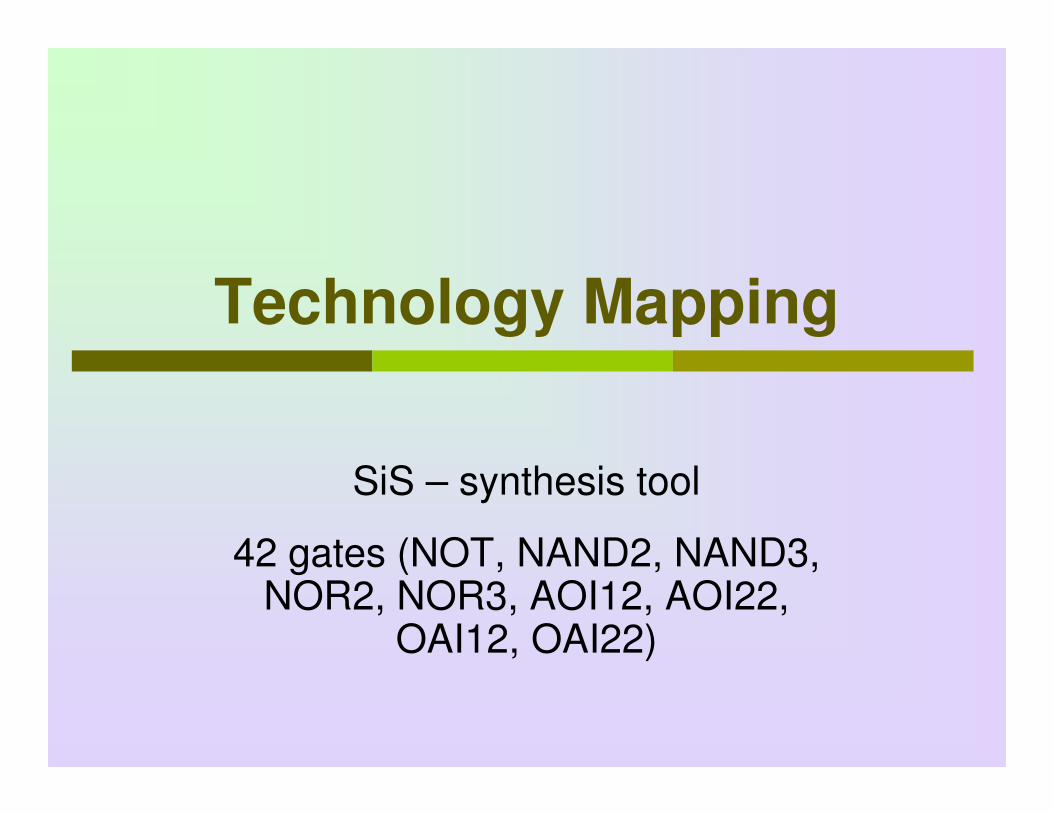
Technology Mapping
SiS – synthesis tool
42 gates (NOT, NAND2, NAND3, NOR2, NOR3, AOI12, AOI22,
OAI12, OAI22)

16
Nominal Synthesis
Library: Delay of gates characterized
assuming no NBTI (Nominal PMOS Vth)
Logic cone: Boolean function
realized at each node
Cost function: Minimum area
that meets the target delay
Compute delay of different candidate
blocks at each node
Choose the structure with the best cost function

17
Library : Delay of gates characterized
for each signal probability
Library: Delay of gates characterized
assuming no NBTI (Nominal PMOS Vth)
NBTI-Aware SP-based Synthesis
Logic cone: Signal
probability propagated from PIs to all nodes in
subject graph
Pick best candidate gate under a new metric for delay
Logic cone: Boolean function
realized at each node
Cost function: Minimum area
that meets the target delay
Compute delay of different candidate
blocks at each node
Choose the structure with the best cost function

18
Subject Graph
NAND-NOT Dual Representation of the Subject Graph
0.6 0.4
0.5 0.5
0.4 0.40.6
0.3 0.70.7
0.18
0.3 0.7
0.3
0.18
0.82
0.574
0.426
b
a
cdba +
c
d

19
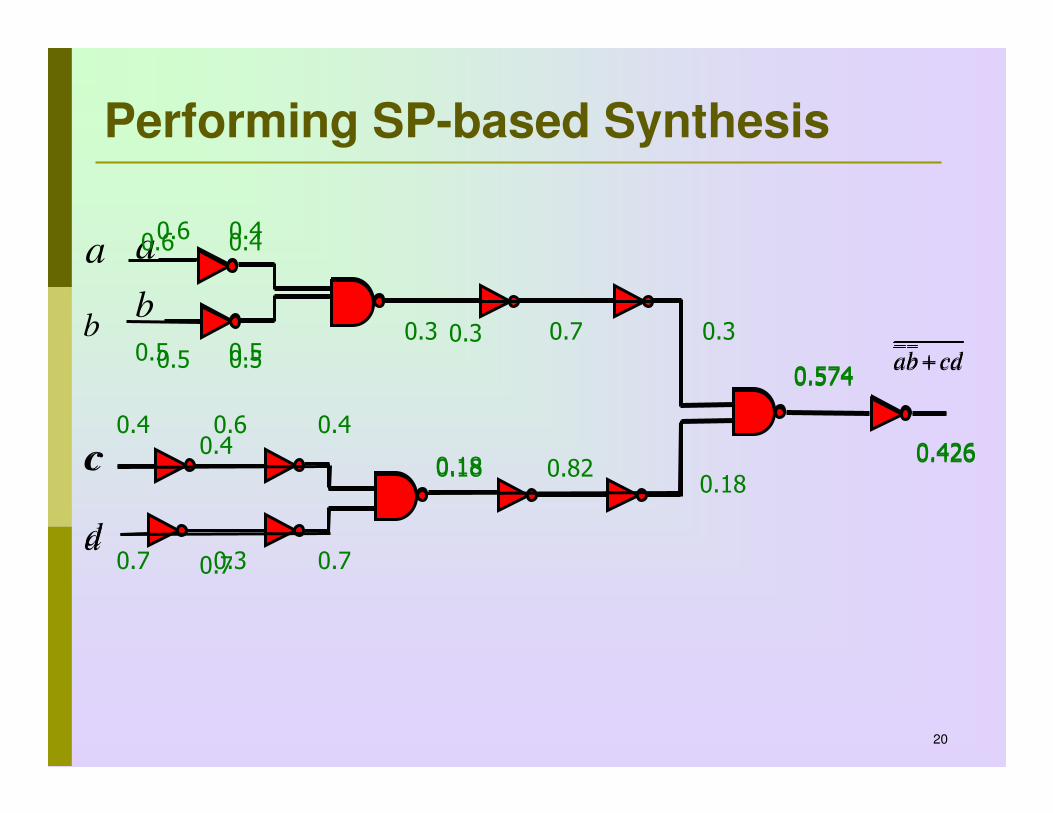
Performing SP-based Synthesis
0.7
a0.6
b0.5
0.3
0.18
0.574
cdba +
0.426
0.82
cdba +
0.426
ba0.6
0.5 0.5
0.4
0.3 0.7
0.4
0.7
0.18 0.82c
d
0.4 0.6
0.30.7
20
Performing SP-based Synthesis
0.6 0.4
0.5 0.5
0.4 0.40.6
0.3 0.70.7
0.18
0.3 0.7 0.3
0.180.82
0.574
0.426
b
a
cdba +
c
d
0.6 0.4
0.5 0.5
0.4
0.7
0.18
0.3
0.574
0.426
b
a
cdba +
c
d

21
Performing SP-based Synthesis
Pushing nodes with large SP inside the gates
0.60.4
0.5
0.5
0.4
0.7
0.18
0.3
0.574 0.426
0.6
0.6
0.3
0.7
0.70.5
0.82
0.4260.4
22
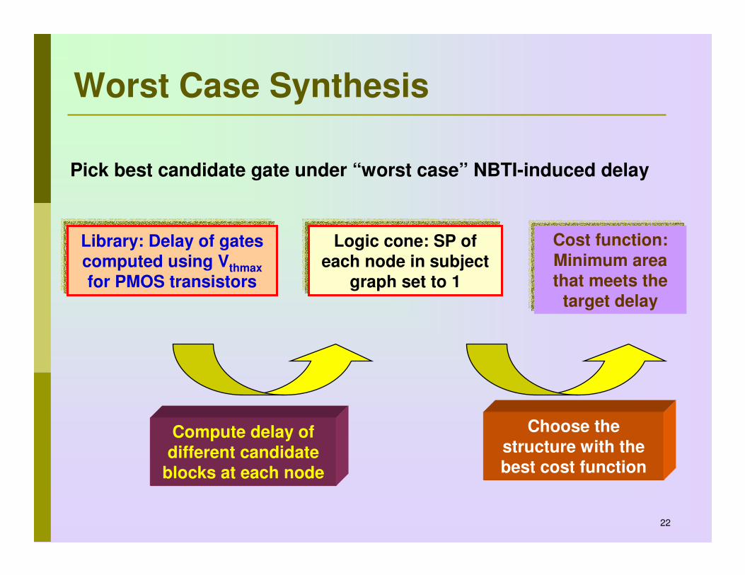
Worst Case Synthesis
Library: Delay of gates computed using Vthmax
for PMOS transistors
Logic cone: SP of each node in subject
graph set to 1
Cost function:
Minimum area that meets the
target delay
Compute delay of
different candidate blocks at each node
Choose the
structure with the best cost function
Pick best candidate gate under “worst case” NBTI-induced delay

C17 - Synthesis Results
Nominal synthesis
Area = 7.4µm
Worst case synthesis
Area = 11.6µm
SP-based synthesis
Area = 9.8µm
Incre
asin
g s
ize
Circuit fails with aging
Tspec = 70ps

24
Temporal Degradation of Circuits
Worst case
SP based
Nominal
10 y
ea
rs
Timing Spec
Data for Benchmark C432

25
Area Delay Curve – Benchmark b1
15
19
23
27
31
35
39
95 100 105 110 115 120 125 130
Delay (ps)
Are
a (
um
)
SP based
worst case

26
Overall Savings
8223619672432088480vda
151261313021491498940alu4
3866186578918738620des
1265969174760923alu2
1438728381744843563200C6288
2020620205725625701100C3540
4117311921221234860C1908
19991810521221282735C1355
Power Savings
(%)
Power (µW)
Area Savings
(%)
Area (µm)
Power (µW)
Area (µm)
Target Delay (ps)
Bench mark
SP basedWorst case

27
Distribution of Gate Types – Benchmark des
0
500
1000
1500
2000
2500
inve
rter
nand2
nand3
nor2nor3ao
i12
oai12
oai22
Gate Type
No
of
Gate
s
Nominal
Worst case
SP based

28
Summary
� NBTI (aging) in circuits causes delay degradation
� Need to relax timing or design NBTI-resilient circuits
� Area increase to counter effect of Vth degradation
� NBTI-aware optimal synthesis method presented
� Signal probability based design reduces pessimism, leads to area savings over “worst case” methods

Thank You
Questions and Comments

Backup

31
Synthesis versus Sizing
2121 XXXXY += X1
X2
Which one is better?
X1
X2
Dela
y
Time of operation (log scale) Target lifetime (log scale)
Are
aSpec
32
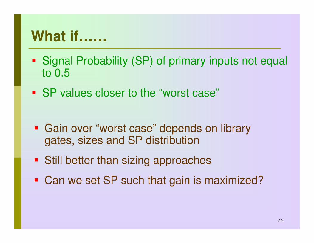
What if……
� Signal Probability (SP) of primary inputs not equal to 0.5
� SP values closer to the “worst case”
� Gain over “worst case” depends on library gates, sizes and SP distribution
� Still better than sizing approaches
� Can we set SP such that gain is maximized?

C17 – Synthesis with Different SP
Worst case synthesis
Area = 11.6µm
0.5 SP-based synthesis
Area = 9.8µm
Incre
asin
g s
ize
0.8 SP-based synthesis
Area = 10.8µm
Tspec = 70ps

34
Converting Random Waveforms to Deterministic Periodic Signals
(SP, AF)
Vdd
k
m k-m
k = m * SP
Vdd
Interface trap count for both these waveforms are equal “asymptotically”

35
Frequency Independence
Number of interface traps for both cases same
Trap generation independent of frequency
freq = f1
freq = f2
T1
T2
n1 cycles
n2 cycles
Vdd
Vdd

36
“sk” Notation – Multi-cycle Model
6/16)( qnsi +
sk=nq+i =
q
p q-p
p/q = SP
Vdd
0 < i ≤ p
5.0
5.0
21
2
−+
−+
+
i
pi
i
piss nqpnq
p < i ≤ q
NIT(kt0) = sk NIT(t0)