ncv4274 - 400 ma voltage regulator family
TRANSCRIPT

© Semiconductor Components Industries, LLC, 2013
November, 2018 − Rev. 161 Publication Order Number:
NCV4274/D
NCV4274, NCV4274A
Regulator Family, 400 mA, 2% and 4% Voltage
DescriptionThe NCV4274 and NCV4274A is a precision micro−power voltage
regulator with an output current capability of 400 mA available in theDPAK, D2PAK and SOT−223 packages.
The output voltage is accurate within ±2.0% or ±4.0% depending onthe version with a maximum dropout voltage of 0.5 V with an input upto 40 V. Low quiescent current is a feature drawing only 150 �A with a1 mA load. This part is ideal for automotive and all battery operatedmicroprocessor equipment.
The regulator is protected against reverse battery, short circuit, andthermal overload conditions. The device can withstand load dumptransients making it suitable for use in automotive environments.
Features• 2.5, 3.3 V, 5.0 V, 8.5 V, ±2.0% Output Options
• 2.5, 3.3 V, 5.0 V, ±4.0% Output Options
• Low 150 �A Quiescent Current at 1 mA load current
• 400 mA Output Current Capability
• Fault Protection
• +60 V Peak Transient Voltage with Respect to GND� −42 V Reverse Voltage� Short Circuit� Thermal Overload
• Very Low Dropout Voltage
• NCV Prefix for Automotive and Other Applications RequiringUnique Site and Control Change Requirements; AEC−Q100Qualified and PPAP Capable
• These are Pb−Free Devices
MARKING DIAGRAMS
DPAKDT SUFFIXCASE 369C
D2PAKDS SUFFIX
CASE 418AF
See detailed ordering and shipping information in the packagedimensions section on page 15 of this data sheet.
ORDERING INFORMATION
www.onsemi.com
74X−xxGALYWW
x
X = A or blankxx = Voltage RatingsA = Assembly LocationL, WL = Wafer LotY = YearWW, W = Work WeekG, � = Pb−Free Package
4
12
3
4
1 2 3
1 Input2, 4 Ground3 Output
1 Input2, 4 Ground3 Output
SOT−223ST SUFFIXCASE 318E 1
AYW74X−xx�
�
1 Input2, 4 Ground3 Output
2 3
4
NCV4274X−xxAWLYWWG
(Note: Microdot may be in either location)
NCV4274, NCV4274A
www.onsemi.com2
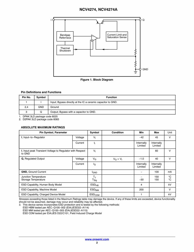
Figure 1. Block Diagram
−+
BandgapRefernece
ThermalShutdown
Current Limit andSaturation Sense
GND
QI
Pin Definitions and Functions
Pin No. Symbol Function
1 I Input; Bypass directly at the IC a ceramic capacitor to GND.
2,4 GND Ground
3 Q Output; Bypass with a capacitor to GND.
1. DPAK 3LD package code 60252. D2PAK 3LD package code 6083
ABSOLUTE MAXIMUM RATINGS
Pin Symbol, Parameter Symbol Condition Min Max Unit
I, Input−to−Regulator Voltage VI −42 45 V
Current II InternallyLimited
InternallyLimited
I, Input peak Transient Voltage to Regulator with Respectto GND
VI 60 V
Q, Regulated Output Voltage VQ VQ = VI −1.0 40 V
Current IQ InternallyLimited
InternallyLimited
GND, Ground Current IGND − 100 mA
Junction TemperatureStorage Temperature
TJTStg
−−50
150150
°C°C
ESD Capability, Human Body Model ESDHB 4 kV
ESD Capability, Machine Model ESDMM 200 V
ESD Capability, Charged Device Model ESDCDM 1 kV
Stresses exceeding those listed in the Maximum Ratings table may damage the device. If any of these limits are exceeded, device functionalityshould not be assumed, damage may occur and reliability may be affected.3. This device series incorporates ESD protection and is tested by the following methods:
ESD HBM tested per AEC−Q100−002 (EIA/JESD22−A114)ESD MM tested per AEC−Q100−003 (EIA/JESD22−A115)ESD CDM tested per EIA/JES D22/C101, Field Induced Charge Model
NCV4274, NCV4274A
www.onsemi.com3
OPERATING RANGE
Parameter Symbol Condition Min Max Unit
Input Voltage (8.5 V Version) VI 9.0 40 V
Input Voltage (5.0 V Version) VI 5.5 40 V
Input Voltage (3.3 V, and 2.5 V Version) VI 4.5 40 V
Junction Temperature TJ −40 150 °C
THERMAL RESISTANCE
Parameter Symbol Condition Min Max Unit
Junction−to−Ambient DPAK Rthja − 70(Note 4)
°C/W
Junction−to−Ambient D2PAK Rthja − 60(Note 4)
°C/W
Junction−to−Case DPAK Rthjc − 4 °C/W
Junction−to−Case D2PAK Rthjc − 3 °C/W
Junction−to−Tab SOT−223 �−JLX,�LX
− 14.5(Note 5)
°C/W
Junction−to−Ambient SOT−223 R�JA, �JA − 169.7(Note 5)
°C/W
4. Soldered in, minimal footprint, FR45. 1 oz copper, 5 mm2 copper area, FR4
LEAD FREE SOLDERING TEMPERATURE AND MSL
Parameter Symbol Condition Min Max Unit
Lead Free Soldering, (Note 6)Reflow (SMD styles only), Pb−Free
Tsld 60s − 150s Above 217s40s Max at Peak − 265 pk
°C
Moisture Sensitivity Level MSL DPAK and D2PAKSOT−223
13
−−
6. Per IPC/JEDEC J−STD−020C

NCV4274, NCV4274A
www.onsemi.com4
ELECTRICAL CHARACTERISTICS−40°C < TJ < 150°C; VI = 13.5 V unless otherwise noted.
Parameter Symbol Test Conditions
Min Typ Max Min Typ Max
UnitNCV4274A NCV4274
REGULATOR
Output Voltage (8.5 V Version) VQ 5 mA < IQ < 200 mA9.5 V < VI < 40 V
8.33 8.5 8.67 − − − V
Output Voltage (8.5 V Version) VQ 5 mA < IQ < 400 mA9.5 V < VI < 28 V
8.33 8.5 8.67 − − − V
Output Voltage (5.0 V Version) VQ 5 mA < IQ < 400 mA6 V < VI < 28 V
4.9 5.0 5.1 4.8 5.0 5.2 V
Output Voltage (5.0 V Version) VQ 5 mA < IQ < 200 mA6 V < VI < 40 V
4.9 5.0 5.1 4.8 5.0 5.2 V
Output Voltage (3.3 V Version) VQ 5 mA < IQ < 400 mA4.5 V < VI < 28 V
3.23 3.3 3.37 3.17 3.3 3.43 V
Output Voltage (3.3 V Version) VQ 5 mA < IQ < 200 mA4.5 V < VI < 40 V
3.23 3.3 3.37 3.17 3.3 3.43 V
Output Voltage (2.5 V Version) VQ 5 mA < IQ < 400 mA4.5 V < VI < 28 V
2.45 2.5 2.55 2.4 2.5 2.6 V
Output Voltage (2.5 V Version) VQ 5 mA < IQ < 200 mA4.5 V < VI < 40 V
2.45 2.5 2.55 2.4 2.5 2.6 V
Current Limit IQ − 400 600 − 400 600 − mA
Quiescent Current Iq IQ = 1 mAVQ = 8.5 VVQ = 5.0 VVQ = 3.3 VVQ = 2.5 V
IQ = 250 mAVQ = 8.5 VVQ = 5.0 VVQ = 3.3 VVQ = 2.5 V
IQ = 400 mAVQ = 8.5 VVQ = 5.0 VVQ = 3.3 VVQ = 2.5 V
−−−−
−−−−
−−−−
195190145140
10101312
20203028
250250250250
15152020
35354545
−−−−
−−−−
−−−−
−190145140
−101312
−203028
−250250250
−152020
−354545
�A�A�A�A
mAmAmAmA
mAmAmAmA
Dropout Voltage
8.5 V Version5.0 V Version3.3 V Version2.5 V Version
VDR IQ = 250 mA, VDR = VI − VQ
VI = 8.5 VVI = 5.0 VVI = 4.5 VVI = 4.5 V
−−−−
250250−−
5005001.272.05
−−−−
−250−−
−5001.332.1
mVmVVV
Load Regulation �VQ IQ = 5 mA to 400 mA − 7 20 − 7 30 mV
Line Regulation �VQ �VI = 12 V to 32 VIQ = 5 mA
− 10 25 − 10 25 mV
Power Supply Ripple Rejection PSRR ƒr = 100 Hz, Vr = 0.5 VPP
− 60 − − 60 − dB
Temperature output voltage drift �VQ/�T − 0.5 − − 0.5 − mV/K
Thermal Shutdown Temperature* TSD IQ = 5 mA 165 − 210 165 − 210 °C
*Guaranteed by design, not tested in production

NCV4274, NCV4274A
www.onsemi.com5
Figure 2. Measuring Circuit
NCV4274NCV4274A
RloadVQ
CQ10 �For22 �F
C12100 nF
C111.0 �F
VQIQQIII
VI
VI
IGND
GND
1 3
2,4
Figure 3. Application Circuit
OutputCQ*CI100 nF
GND
NCV4274NCV4274A
1 3
2,4
Input
VQVI
*CQ = 10 �F for VQ ≤ 3.3 V CQ = 22 �F for VQ ≥ 5 V
TYPICAL CHARACTERISTIC CURVES
Figure 4. ESR Characterization − 3.3 V, 5 V and8.5 V Versions
0.01
0.1
1
10
100
0 50 100 150 200 250
ES
R (�
)
LOAD CURRENT (mA)
Maximum ESRCOUT = 10 �F − 100 �F
300 350 400
Stable Region
VI = 13.5 V
Figure 5. ESR Characterization − 2.5 V Version
0.1
1.0
10
100
1000
0 5 20 60 100 140
ES
R (�
)
LOAD CURRENT (mA)
Maximum ESRCOUT = 1 �F − 100 �F
180 220 260 300 340 380 420
Minimum ESRCOUT = 1 �F
Stable Region
VI = 13.5 V
NCV4274, NCV4274A
www.onsemi.com6
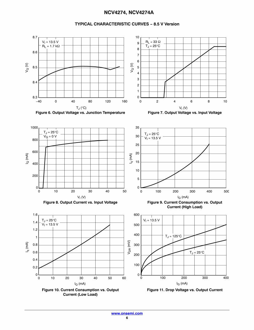
TYPICAL CHARACTERISTIC CURVES − 8.5 V Version
8.3
8.4
8.5
8.6
8.7
−40 0 40 80 120 160
VQ
(V
)
TJ (°C)
0
1
2
3
4
5
6
0 2 4 6 8 10
RL = 33 �TJ = 25°C
VI = 13.5 VRL = 1.7 k�
VQ
(V
)
VI (V)
Figure 6. Output Voltage vs. Junction Temperature
0
200
400
600
1000
0 10 20 30 40 50
I Q (
mA
)
VI (V)
Figure 7. Output Voltage vs. Input Voltage
TJ = 25°CVQ = 0 V
0
5
10
15
20
25
35
0 100 200 300 400 500
I q (
mA
)
IQ (mA)
Figure 8. Output Current vs. Input Voltage
TJ = 25°CVI = 13.5 V
0
0.2
0.4
0.6
0.8
1
1.2
1.4
1.6
0 10 20 30 40 50 60
I q (
mA
)
IQ (mA)
TJ = 25°CVI = 13.5 V
Figure 9. Current Consumption vs. OutputCurrent (High Load)
Figure 10. Current Consumption vs. OutputCurrent (Low Load)
Figure 11. Drop Voltage vs. Output Current
0
100
200
300
400
500
600
0 100 200 300 400
VD
R (
mV
)
IQ (mA)
TJ = 25°C
TJ = 125°C
7
8
9
10
80030
VI = 13.5 V
NCV4274, NCV4274A
www.onsemi.com7
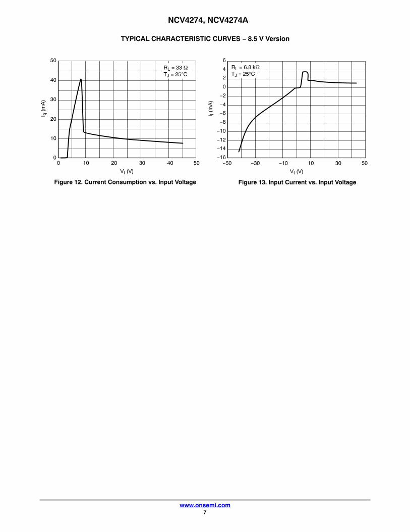
TYPICAL CHARACTERISTIC CURVES − 8.5 V Version
0
10
20
30
50
0 10 20 30 40 50
RL = 33 �TJ = 25°C
I q (
mA
)
VI (V)
−16
−14
−12
−10
−8
−6
−4
−2
0
2
4
6
−50 −30 −10 30 50
RL = 6.8 k�TJ = 25°C
I I (m
A)
VI (V)
Figure 12. Current Consumption vs. Input Voltage Figure 13. Input Current vs. Input Voltage
40
10

NCV4274, NCV4274A
www.onsemi.com8
TYPICAL CHARACTERISTIC CURVES − 5.0 V Version
4.8
4.9
5.0
5.1
5.2
−40 0 40 80 120 160
VQ
(V
)
TJ (°C)
0
1
2
3
4
5
6
0 2 4 6 8 10
RL = 20 �TJ = 25°C
VI = 13.5 VRL = 1 k�
VQ
(V
)
VI (V)
Figure 14. Output Voltage vs. JunctionTemperature
0
200
400
600
800
0 10 20 30 40 50
I Q (
mA
)
VI (V)
Figure 15. Output Voltage vs. Input Voltage
TJ = 25°CVQ = 0 V
0
10
20
30
40
50
60
0 100 200 300 400 500 600
I q (
mA
)
IQ (mA)
Figure 16. Output Current vs. Input Voltage
TJ = 25°CVI = 13.5 V
0
0.2
0.4
0.6
0.8
1
1.2
1.4
1.6
0 10 20 30 40 50 60
I q (
mA
)
IQ (mA)
TJ = 25°CVI = 13.5 V
Figure 17. Current Consumption vs. OutputCurrent (High Load)
Figure 18. Current Consumption vs. OutputCurrent (Low Load)
Figure 19. Drop Voltage vs. Output Current
0
100
200
300
400
500
600
0 100 200 300 400
VD
R (
mV
)
IQ (mA)
TJ = 25°C
TJ = 125°C

NCV4274, NCV4274A
www.onsemi.com9
TYPICAL CHARACTERISTIC CURVES − 5.0 V Version
0
10
20
30
40
0 10 20 30 40 50
RL = 20 �TJ = 25°C
I q (
mA
)
VI (V)
−16
−14
−12
−10
−8
−6
−4
−2
0
2
4
6
−50 −25 0 25 50
RL = 6.8 k�TJ = 25°C
I I (m
A)
VI (V)
Figure 20. Current Consumption vs. Input Voltage Figure 21. Input Current vs. Input Voltage

NCV4274, NCV4274A
www.onsemi.com10
TYPICAL CHARACTERISTIC CURVES − 3.3 V Version
2.9
3.0
3.1
3.4
3.5
−40 0 40 80 120 160
VQ
(V
)
TJ (°C)
0
1
2
3
4
5
6
0 1 3 4 5 6
RL = 20 �TJ = 25°C
VI = 6 VRL = 1 k�
VQ
(V
)
VI (V)
Figure 22. Output Voltage vs. JunctionTemperature
0
200
400
600
800
0 10 20 30 40 50
I Q (
mA
)
VI (V)
Figure 23. Output Voltage vs. Input Voltage
TJ = 25°CVQ = 0 V
0
10
20
30
40
50
60
0 100 200 300 400 500 600
I q (
mA
)
IQ (mA)
Figure 24. Output Current vs. Input Voltage
TJ = 25°CVI = 13.5 V
0
0.2
0.4
0.6
0.8
1.0
1.2
1.4
1.6
0 10 20 30 40 50 60
I q (
mA
)
IQ (mA)
TJ = 25°CVI = 13.5 V
Figure 25. Current Consumption vs. OutputCurrent (High Load)
Figure 26. Current Consumption vs. OutputCurrent (Low Load)
Figure 27. Voltage Drop vs. Output Current
1.14
1.16
1.18
1.20
1.22
1.24
1.26
0 100 200 300 400
VD
R (
V)
IQ (mA)
TJ = 25°C
TJ = 125°C
3.2
3.3
2
VDR = VI(min) − VQ
NCV4274, NCV4274A
www.onsemi.com11
TYPICAL CHARACTERISTIC CURVES − 3.3 V Version
0
1
4
5
7
0 10 20 30 40 50
RL = 20 �TJ = 25°C
I q (
mA
)
VI (V)
−16
−14
−12
−10
−8
−6
−4
−2
0
2
4
−50 −25 0 25 50
RL = 3.3 k�TJ = 25°C
I I (m
A)
VI (V)
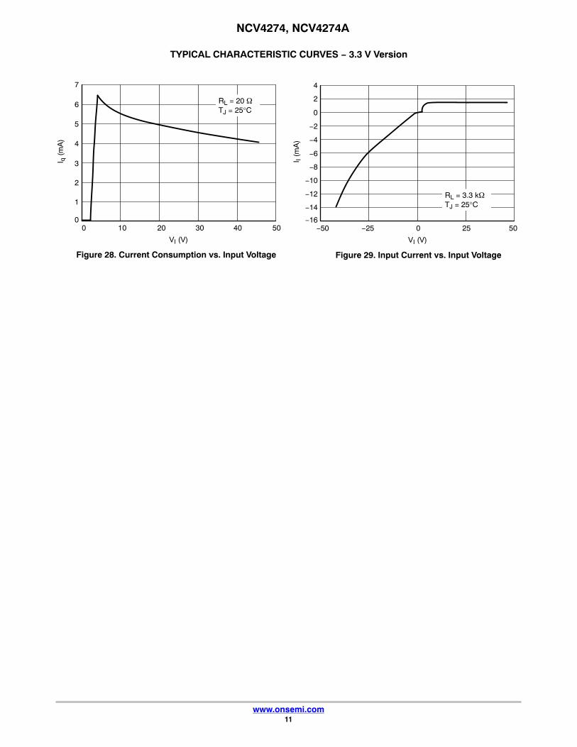
Figure 28. Current Consumption vs. Input Voltage Figure 29. Input Current vs. Input Voltage
2
3
6

NCV4274, NCV4274A
www.onsemi.com12
TYPICAL CHARACTERISTIC CURVES − 2.5 V Version
2.1
2.2
2.3
2.6
2.7
−40 0 40 80 120 160
VQ
(V
)
TJ (°C)
0
1.0
2.0
3.0
4.0
4.5
5.0
0 1 3 4 5 6
VI = 6 VRL = 1 k�
VQ
(V
)
VI (V)
Figure 30. Output Voltage vs. JunctionTemperature
0
200
400
600
800
0 10 20 30 40 50
I Q (
mA
)
VI (V)
Figure 31. Output Voltage vs. Input Voltage
TJ = 25°CVQ = 0 V
0
10
20
30
40
50
60
0 100 200 300 400 500 600
I q (
mA
)
IQ (mA)
Figure 32. Output Current vs. Input Voltage
TJ = 25°CVI = 13.5 V
0
0.2
0.4
0.6
0.8
1.0
1.2
1.4
1.6
0 10 20 30 40 50 60
I q (
mA
)
IQ (mA)
TJ = 25°CVI = 13.5 V
Figure 33. Current Consumption vs. OutputCurrent (High Load)
Figure 34. Current Consumption vs. OutputCurrent (Low Load)
Figure 35. Voltage Drop vs. Output Current
1.95
1.96
1.97
2.00
2.02
2.03
2.05
0 100 200 300 400
VD
R (
V)
IQ (mA)
TJ = 25°C
TJ = 125°C
2.4
2.5
2
VDR = VI(min) − VQ
3.5
0.5
1.5
2.5
1.98
1.99
2.01
2.04
NCV4274, NCV4274A
www.onsemi.com13
TYPICAL CHARACTERISTIC CURVES − 2.5 V Version
0
0.5
2.5
3.0
4.5
0 10 20 30 40 50
RL = 20 �TJ = 25°C
I q (
mA
)
VI (V)
−14
−12
−10
−8
−6
−4
−2
0
2
−50 −25 0 25 50
RL = 3.3 k�TJ = 25°C
I I (m
A)
VI (V)
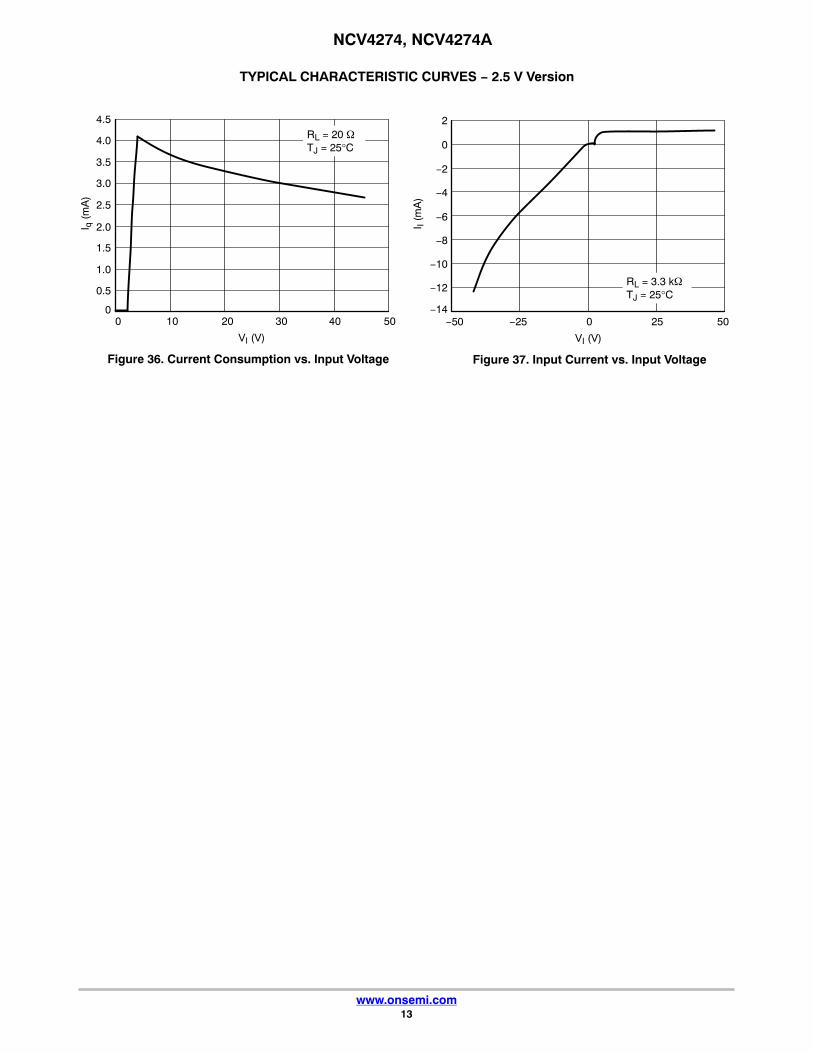
Figure 36. Current Consumption vs. Input Voltage Figure 37. Input Current vs. Input Voltage
1.0
1.5
4.0
2.0
3.5

NCV4274, NCV4274A
www.onsemi.com14
APPLICATION DESCRIPTION
Output RegulatorThe output is controlled by a precision trimmed reference
and error amplifier. The PNP output has saturation controlfor regulation while the input voltage is low, preventing oversaturation. Current limit and voltage monitors complementthe regulator design to give safe operating signals to theprocessor and control circuits.
Stability ConsiderationsThe input capacitor CI1 in Figure 2 is necessary for
compensating input line reactance. Possible oscillationscaused by input inductance and input capacitance can bedamped by using a resistor of approximately 1 � in serieswith CI2.
The output or compensation capacitor helps determinethree main characteristics of a linear regulator: startup delay,load transient response and loop stability.
The capacitor value and type should be based on cost,availability, size and temperature constraints. Thealuminum electrolytic capacitor is the least expensivesolution, but, if the circuit operates at low temperatures(−25°C to −40°C), both the value and ESR of the capacitorwill vary considerably. The capacitor manufacturer’s datasheet usually provides this information.
The value for the output capacitor CQ shown in Figure 2should work for most applications; however, it is notnecessarily the optimized solution. Stability is guaranteed atvalues CQ � 2.2 �F and an ESR � 2.5 � within theoperating temperature range. Actual limits are shown in agraph in the Typical Performance Characteristics section.
Calculating Power Dissipation in a Single OutputLinear Regulator
The maximum power dissipation for a single outputregulator (Figure 3) is:
PD(max) � [VI(max) � VQ(min)]IQ(max) � VI(max)Iq (eq. 1)
Where:VI(max) is the maximum input voltage,VQ(min) is the minimum output voltage,IQ(max) is the maximum output current for the application,andIq is the quiescent current the regulator consumes at IQ(max).
Once the value of PD(max) is known, the maximumpermissible value of R�JA can be calculated:
P�JA�
�150 C � TA�
PD
(eq. 2)
The value of R�JA can then be compared with those in thepackage section of the data sheet. Those packages withR�JA’s less than the calculated value in Equation 2 will keepthe die temperature below 150°C. In some cases, none of thepackages will be sufficient to dissipate the heat generated bythe IC, and an external heat sink will be required. The currentflow and voltages are shown in the Measurement CircuitDiagram.
Heat SinksA heat sink effectively increases the surface area of the
package to improve the flow of heat away from the IC andinto the surrounding air.
Each material in the heat flow path between the IC and theoutside environment will have a thermal resistance. Likeseries electrical resistances, these resistances are summed todetermine the value of R�JA:
R�JA � R�JC � R�CS � R�SA (eq. 3)
Where:R�JC = the junction−to−case thermal resistance,R�CS = the case−to−heat sink thermal resistance, andR�SA = the heat sink−to−ambient thermal resistance.R�JC appears in the package section of the data sheet.
Like R�JA, it too is a function of package type. R�CS andR�SA are functions of the package type, heat sink and theinterface between them. These values appear in data sheetsof heat sink manufacturers. Thermal, mounting, andheat sinking are discussed in the ON Semiconductorapplication note AN1040/D, available on theON Semiconductor Website.
NCV4274, NCV4274A
www.onsemi.com15
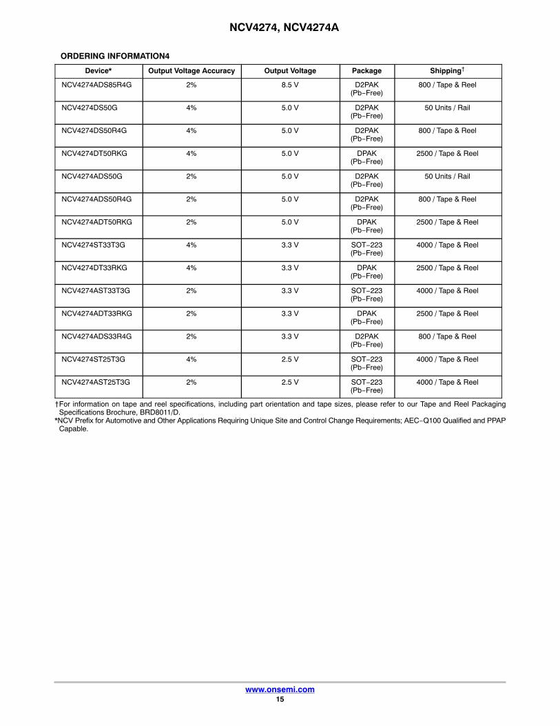
ORDERING INFORMATION4
Device* Output Voltage Accuracy Output Voltage Package Shipping†
NCV4274ADS85R4G 2% 8.5 V D2PAK(Pb−Free)
800 / Tape & Reel
NCV4274DS50G 4% 5.0 V D2PAK(Pb−Free)
50 Units / Rail
NCV4274DS50R4G 4% 5.0 V D2PAK(Pb−Free)
800 / Tape & Reel
NCV4274DT50RKG 4% 5.0 V DPAK(Pb−Free)
2500 / Tape & Reel
NCV4274ADS50G 2% 5.0 V D2PAK(Pb−Free)
50 Units / Rail
NCV4274ADS50R4G 2% 5.0 V D2PAK(Pb−Free)
800 / Tape & Reel
NCV4274ADT50RKG 2% 5.0 V DPAK(Pb−Free)
2500 / Tape & Reel
NCV4274ST33T3G 4% 3.3 V SOT−223(Pb−Free)
4000 / Tape & Reel
NCV4274DT33RKG 4% 3.3 V DPAK(Pb−Free)
2500 / Tape & Reel
NCV4274AST33T3G 2% 3.3 V SOT−223(Pb−Free)
4000 / Tape & Reel
NCV4274ADT33RKG 2% 3.3 V DPAK(Pb−Free)
2500 / Tape & Reel
NCV4274ADS33R4G 2% 3.3 V D2PAK(Pb−Free)
800 / Tape & Reel
NCV4274ST25T3G 4% 2.5 V SOT−223(Pb−Free)
4000 / Tape & Reel
NCV4274AST25T3G 2% 2.5 V SOT−223(Pb−Free)
4000 / Tape & Reel
†For information on tape and reel specifications, including part orientation and tape sizes, please refer to our Tape and Reel PackagingSpecifications Brochure, BRD8011/D.
*NCV Prefix for Automotive and Other Applications Requiring Unique Site and Control Change Requirements; AEC−Q100 Qualified and PPAPCapable.
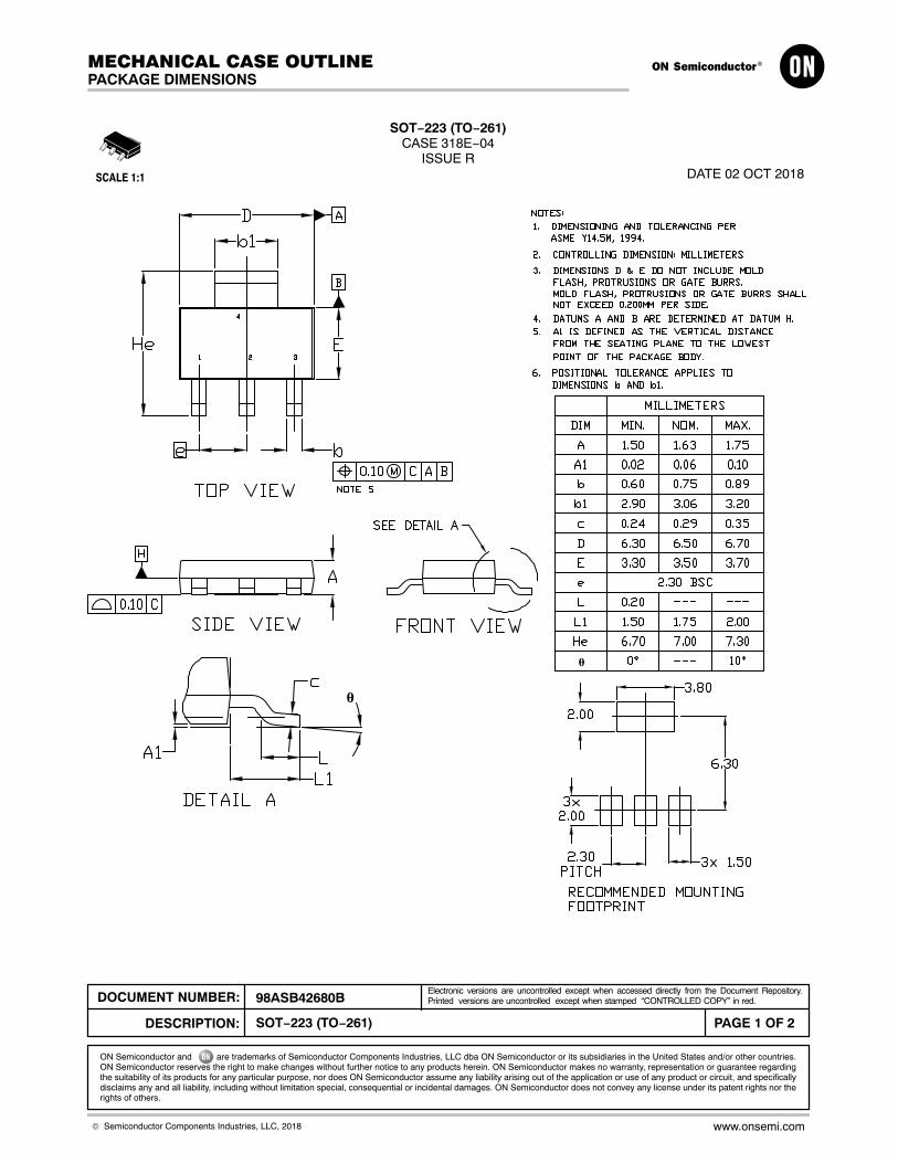
SOT−223 (TO−261)CASE 318E−04
ISSUE RDATE 02 OCT 2018SCALE 1:1
�
�
MECHANICAL CASE OUTLINE
PACKAGE DIMENSIONS
ON Semiconductor and are trademarks of Semiconductor Components Industries, LLC dba ON Semiconductor or its subsidiaries in the United States and/or other countries.ON Semiconductor reserves the right to make changes without further notice to any products herein. ON Semiconductor makes no warranty, representation or guarantee regardingthe suitability of its products for any particular purpose, nor does ON Semiconductor assume any liability arising out of the application or use of any product or circuit, and specificallydisclaims any and all liability, including without limitation special, consequential or incidental damages. ON Semiconductor does not convey any license under its patent rights nor therights of others.
98ASB42680BDOCUMENT NUMBER:
DESCRIPTION:
Electronic versions are uncontrolled except when accessed directly from the Document Repository.Printed versions are uncontrolled except when stamped “CONTROLLED COPY” in red.
PAGE 1 OF 2SOT−223 (TO−261)
© Semiconductor Components Industries, LLC, 2018 www.onsemi.com
SOT−223 (TO−261)CASE 318E−04
ISSUE RDATE 02 OCT 2018
STYLE 4:PIN 1. SOURCE
2. DRAIN3. GATE4. DRAIN
STYLE 6:PIN 1. RETURN
2. INPUT3. OUTPUT4. INPUT
STYLE 8:CANCELLED
STYLE 1:PIN 1. BASE
2. COLLECTOR3. EMITTER4. COLLECTOR
STYLE 10:PIN 1. CATHODE
2. ANODE3. GATE4. ANODE
STYLE 7:PIN 1. ANODE 1
2. CATHODE3. ANODE 24. CATHODE
STYLE 3:PIN 1. GATE
2. DRAIN3. SOURCE4. DRAIN
STYLE 2:PIN 1. ANODE
2. CATHODE3. NC4. CATHODE
STYLE 9:PIN 1. INPUT
2. GROUND3. LOGIC4. GROUND
STYLE 5:PIN 1. DRAIN
2. GATE3. SOURCE4. GATE
STYLE 11:PIN 1. MT 1
2. MT 23. GATE4. MT 2
STYLE 12:PIN 1. INPUT
2. OUTPUT3. NC4. OUTPUT
STYLE 13:PIN 1. GATE
2. COLLECTOR3. EMITTER4. COLLECTOR
1
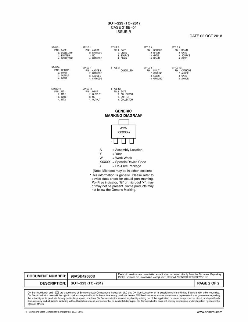
A = Assembly LocationY = YearW = Work WeekXXXXX = Specific Device Code� = Pb−Free Package
GENERICMARKING DIAGRAM*
AYWXXXXX�
�
(Note: Microdot may be in either location)*This information is generic. Please refer to
device data sheet for actual part marking.Pb−Free indicator, “G” or microdot “�”, mayor may not be present. Some products maynot follow the Generic Marking.
ON Semiconductor and are trademarks of Semiconductor Components Industries, LLC dba ON Semiconductor or its subsidiaries in the United States and/or other countries.ON Semiconductor reserves the right to make changes without further notice to any products herein. ON Semiconductor makes no warranty, representation or guarantee regardingthe suitability of its products for any particular purpose, nor does ON Semiconductor assume any liability arising out of the application or use of any product or circuit, and specificallydisclaims any and all liability, including without limitation special, consequential or incidental damages. ON Semiconductor does not convey any license under its patent rights nor therights of others.
98ASB42680BDOCUMENT NUMBER:
DESCRIPTION:
Electronic versions are uncontrolled except when accessed directly from the Document Repository.Printed versions are uncontrolled except when stamped “CONTROLLED COPY” in red.
PAGE 2 OF 2SOT−223 (TO−261)
© Semiconductor Components Industries, LLC, 2018 www.onsemi.com

DPAK (SINGLE GAUGE)CASE 369C
ISSUE FDATE 21 JUL 2015
SCALE 1:1
STYLE 1:PIN 1. BASE
2. COLLECTOR3. EMITTER4. COLLECTOR
STYLE 2:PIN 1. GATE
2. DRAIN3. SOURCE4. DRAIN
STYLE 3:PIN 1. ANODE
2. CATHODE3. ANODE4. CATHODE
STYLE 4:PIN 1. CATHODE
2. ANODE3. GATE4. ANODE
STYLE 5:PIN 1. GATE
2. ANODE3. CATHODE4. ANODE
STYLE 6:PIN 1. MT1
2. MT23. GATE4. MT2
STYLE 7:PIN 1. GATE
2. COLLECTOR3. EMITTER4. COLLECTOR
1 23
4
STYLE 8:PIN 1. N/C
2. CATHODE3. ANODE4. CATHODE
STYLE 9:PIN 1. ANODE
2. CATHODE3. RESISTOR ADJUST4. CATHODE
STYLE 10:PIN 1. CATHODE
2. ANODE3. CATHODE4. ANODE
b
D
E
b3
L3
L4b2
M0.005 (0.13) C
c2
A
c
C
Z
DIM MIN MAX MIN MAXMILLIMETERSINCHES
D 0.235 0.245 5.97 6.22E 0.250 0.265 6.35 6.73
A 0.086 0.094 2.18 2.38
b 0.025 0.035 0.63 0.89
c2 0.018 0.024 0.46 0.61
b2 0.028 0.045 0.72 1.14
c 0.018 0.024 0.46 0.61
e 0.090 BSC 2.29 BSC
b3 0.180 0.215 4.57 5.46
L4 −−− 0.040 −−− 1.01
L 0.055 0.070 1.40 1.78
L3 0.035 0.050 0.89 1.27
Z 0.155 −−− 3.93 −−−
NOTES:1. DIMENSIONING AND TOLERANCING PER ASME
Y14.5M, 1994.2. CONTROLLING DIMENSION: INCHES.3. THERMAL PAD CONTOUR OPTIONAL WITHIN DI-
MENSIONS b3, L3 and Z.4. DIMENSIONS D AND E DO NOT INCLUDE MOLD
FLASH, PROTRUSIONS, OR BURRS. MOLDFLASH, PROTRUSIONS, OR GATE BURRS SHALLNOT EXCEED 0.006 INCHES PER SIDE.
5. DIMENSIONS D AND E ARE DETERMINED AT THEOUTERMOST EXTREMES OF THE PLASTIC BODY.
6. DATUMS A AND B ARE DETERMINED AT DATUMPLANE H.
7. OPTIONAL MOLD FEATURE.
1 2 3
4
XXXXXX = Device CodeA = Assembly LocationL = Wafer LotY = YearWW = Work WeekG = Pb−Free Package
AYWWXXXXXXXXG
XXXXXXGALYWW
DiscreteIC
5.800.228
2.580.102
1.600.063
6.200.244
3.000.118
6.170.243
� mminches
�SCALE 3:1
GENERICMARKING DIAGRAM*
*This information is generic. Please referto device data sheet for actual partmarking.
*For additional information on our Pb−Free strategy and solderingdetails, please download the ON Semiconductor Soldering andMounting Techniques Reference Manual, SOLDERRM/D.
SOLDERING FOOTPRINT*
H 0.370 0.410 9.40 10.41
A1 0.000 0.005 0.00 0.13
L1 0.114 REF 2.90 REFL2 0.020 BSC 0.51 BSC
A1
HDETAIL A
SEATINGPLANE
A
B
C
L1L
H
L2 GAUGEPLANE
DETAIL AROTATED 90 CW�
eBOTTOM VIEW
Z
BOTTOM VIEW
SIDE VIEW
TOP VIEW
ALTERNATECONSTRUCTIONS
NOTE 7
Z
MECHANICAL CASE OUTLINE
PACKAGE DIMENSIONS
http://onsemi.com1
© Semiconductor Components Industries, LLC, 2002
October, 2002 − Rev. 0Case Outline Number:
XXX
DOCUMENT NUMBER:
STATUS:
NEW STANDARD:
DESCRIPTION:
98AON10527D
ON SEMICONDUCTOR STANDARD
REF TO JEDEC TO−252
DPAK SINGLE GAUGE SURFACE MOUNT
Electronic versions are uncontrolled except when accessed directly from the Document Repository. Printed versions are uncontrolled except when stamped “CONTROLLED COPY” in red.
PAGE 1 OF 2
DOCUMENT NUMBER:98AON10527D
PAGE 2 OF 2
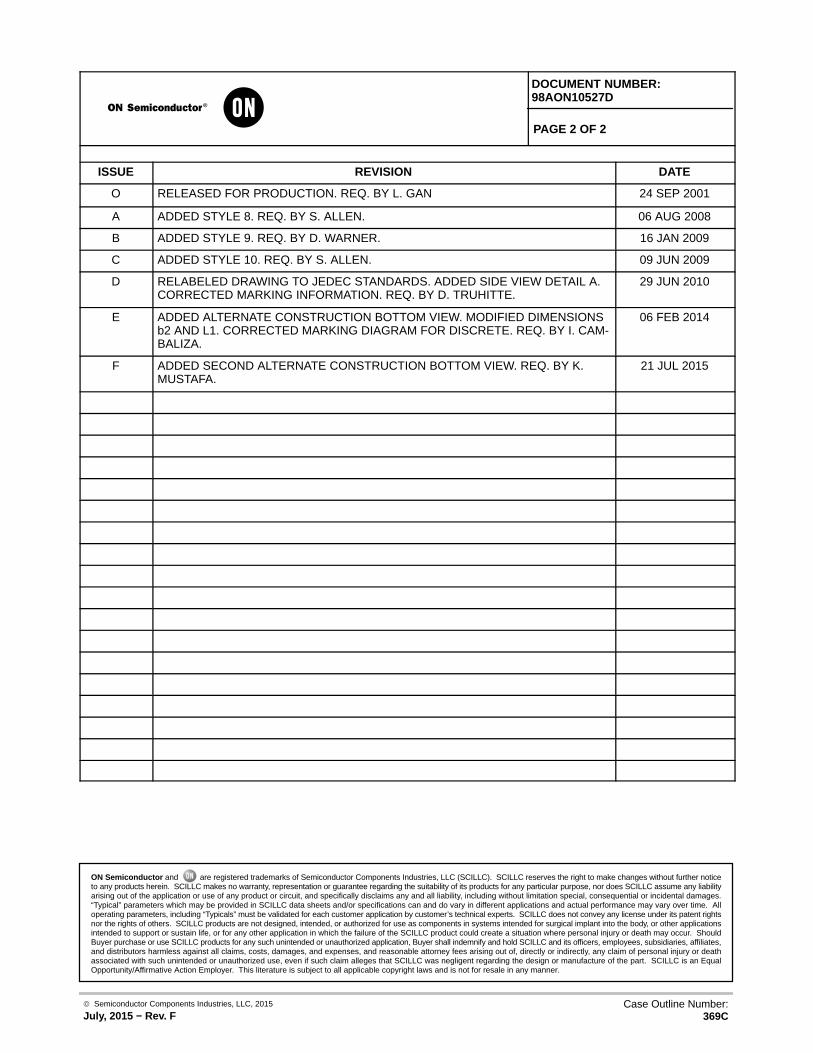
ISSUE REVISION DATE
O RELEASED FOR PRODUCTION. REQ. BY L. GAN 24 SEP 2001
A ADDED STYLE 8. REQ. BY S. ALLEN. 06 AUG 2008
B ADDED STYLE 9. REQ. BY D. WARNER. 16 JAN 2009
C ADDED STYLE 10. REQ. BY S. ALLEN. 09 JUN 2009
D RELABELED DRAWING TO JEDEC STANDARDS. ADDED SIDE VIEW DETAIL A.CORRECTED MARKING INFORMATION. REQ. BY D. TRUHITTE.
29 JUN 2010
E ADDED ALTERNATE CONSTRUCTION BOTTOM VIEW. MODIFIED DIMENSIONSb2 AND L1. CORRECTED MARKING DIAGRAM FOR DISCRETE. REQ. BY I. CAM-BALIZA.
06 FEB 2014
F ADDED SECOND ALTERNATE CONSTRUCTION BOTTOM VIEW. REQ. BY K.MUSTAFA.
21 JUL 2015
© Semiconductor Components Industries, LLC, 2015
July, 2015 − Rev. FCase Outline Number:
369C
ON Semiconductor and are registered trademarks of Semiconductor Components Industries, LLC (SCILLC). SCILLC reserves the right to make changes without further noticeto any products herein. SCILLC makes no warranty, representation or guarantee regarding the suitability of its products for any particular purpose, nor does SCILLC assume any liabilityarising out of the application or use of any product or circuit, and specifically disclaims any and all liability, including without limitation special, consequential or incidental damages.“Typical” parameters which may be provided in SCILLC data sheets and/or specifications can and do vary in different applications and actual performance may vary over time. Alloperating parameters, including “Typicals” must be validated for each customer application by customer’s technical experts. SCILLC does not convey any license under its patent rightsnor the rights of others. SCILLC products are not designed, intended, or authorized for use as components in systems intended for surgical implant into the body, or other applicationsintended to support or sustain life, or for any other application in which the failure of the SCILLC product could create a situation where personal injury or death may occur. ShouldBuyer purchase or use SCILLC products for any such unintended or unauthorized application, Buyer shall indemnify and hold SCILLC and its officers, employees, subsidiaries, affiliates,and distributors harmless against all claims, costs, damages, and expenses, and reasonable attorney fees arising out of, directly or indirectly, any claim of personal injury or deathassociated with such unintended or unauthorized use, even if such claim alleges that SCILLC was negligent regarding the design or manufacture of the part. SCILLC is an EqualOpportunity/Affirmative Action Employer. This literature is subject to all applicable copyright laws and is not for resale in any manner.

http://onsemi.com1
D2PAKCASE 418AF
ISSUE EDATE 15 SEP 2015
SCALE 1:1
XXXXXXXXXXXAWLYYWWG
XXXXX = Specific Device CodeA = Assembly LocationWL = Wafer LotYY = YearWW = Work WeekG = Pb−Free Package
GENERICMARKING DIAGRAM*
*This information is generic. Please referto device data sheet for actual partmarking. Pb−Free indicator, “G”, mayor not be present.
V
U
TERMINAL 4
NOTES:1. DIMENSIONING AND TOLERANCING PER ANSI
Y14.5M, 1982.2. CONTROLLING DIMENSION: INCHES.3. TAB CONTOUR OPTIONAL WITHIN DIMENSIONS
A AND K.4. DIMENSIONS U AND V ESTABLISH A MINIMUM
MOUNTING SURFACE FOR TERMINAL 4.5. DIMENSIONS A AND B DO NOT INCLUDE MOLD
FLASH OR GATE PROTRUSIONS. MOLD FLASHAND GATE PROTRUSIONS NOT TO EXCEED0.025 (0.635) MAXIMUM.
6. SINGLE GAUGE DESIGN WILL BE SHIPPEDAFTER FPCN EXPIRATION IN OCTOBER 2011.
DIMA
MIN MAX MIN MAXMILLIMETERS
0.386 0.403 9.804 10.236
INCHES
B 0.356 0.368 9.042 9.347C 0.170 0.180 4.318 4.572D 0.026 0.036 0.660 0.914E 0.045 0.055 1.143 1.397
F 0.051 REF 1.295 REFG 0.100 BSC 2.540 BSCH 0.539 0.579 13.691 14.707J 0.125 MAX 3.175 MAXK 0.050 REF 1.270 REFL 0.000 0.010 0.000 0.254M 0.088 0.102 2.235 2.591N 0.018 0.026 0.457 0.660P 0.058 0.078 1.473 1.981RS 0.116 REF 2.946 REFU 0.200 MIN 5.080 MINV 0.250 MIN 6.350 MIN
A
1 2 3
K
F
B
J
S
H
DM0.010 (0.254) T
EOPTIONALCHAMFER
BOTTOM VIEWOPTIONAL CONSTRUCTIONS
TOP VIEW
SIDE VIEWDUAL GAUGE
BOTTOM VIEW
L
T
P
R DETAIL C
SEATINGPLANE
3XG
N M
CONSTRUCTION
D
C
DETAIL C
EOPTIONALCHAMFER
SIDE VIEWSINGLE GAUGECONSTRUCTION
S
C
DETAIL C
TT
D
E 0.018 0.026 0.457 0.660S
*For additional information on our Pb−Free strategy and solderingdetails, please download the ON Semiconductor Soldering andMounting Techniques Reference Manual, SOLDERRM/D.
SOLDERING FOOTPRINT*
8.380
2.540
DIMENSIONS: MILLIMETERSPITCH
3X
16.155
1.0163X
10.490
3.504
0� 8� 0� 8�
MECHANICAL CASE OUTLINE
PACKAGE DIMENSIONS
http://onsemi.com1
© Semiconductor Components Industries, LLC, 2002
October, 2002 − Rev. 0Case Outline Number:
XXX
DOCUMENT NUMBER:
STATUS:
NEW STANDARD:
DESCRIPTION:
98AON21981D
ON SEMICONDUCTOR STANDARD
D2PAK, 3 LEAD, NON−CROPPED
Electronic versions are uncontrolled except when accessed directly from the Document Repository. Printed versions are uncontrolled except when stamped “CONTROLLED COPY” in red.
PAGE 1 OF 2

http://onsemi.com2
DOCUMENT NUMBER:98AON21981D
PAGE 2 OF 2
ISSUE REVISION DATE
O RELEASED FOR PRODUCTION. REQ. BY A. NOAH. 13 FEB 2006
A ADDED SOLDERING FOOTPRINT. REQ. BY M. FILLION. 18 JUN 2007
B ADDED SINGLE AND DUAL GAUGE SIDE VIEWS AND BOTTOM VIEW. REQ. BYJ. KREMMER.
08 NOV 2011
C CORRECTED SOLDERING FOOTPRINT TO VERSION FROM ISSUE A. REQ. BYJ. KREMMER.
13 APR 2012
D CORRECTED SOLDERING FOOTPRINT BACK TO VERSION FROM ISSUE B.REQ. BY J. KREMMER.
24 MAY 2012
E REVISED DIMENSION R FROM 5 DEGREES REFERENCE TO 0 & 8 DEGREESMIN & MAX. REQ. BY K. MUSTAFA.
15 SEP 2015
© Semiconductor Components Industries, LLC, 2015
September, 2015 − Rev. ECase Outline Number:
418AF
ON Semiconductor and are registered trademarks of Semiconductor Components Industries, LLC (SCILLC). SCILLC reserves the right to make changes without further noticeto any products herein. SCILLC makes no warranty, representation or guarantee regarding the suitability of its products for any particular purpose, nor does SCILLC assume anyliability arising out of the application or use of any product or circuit, and specifically disclaims any and all liability, including without limitation special, consequential or incidentaldamages. “Typical” parameters which may be provided in SCILLC data sheets and/or specifications can and do vary in different applications and actual performance may vary overtime. All operating parameters, including “Typicals” must be validated for each customer application by customer’s technical experts. SCILLC does not convey any license underits patent rights nor the rights of others. SCILLC products are not designed, intended, or authorized for use as components in systems intended for surgical implant into the body,or other applications intended to support or sustain life, or for any other application in which the failure of the SCILLC product could create a situation where personal injury or deathmay occur. Should Buyer purchase or use SCILLC products for any such unintended or unauthorized application, Buyer shall indemnify and hold SCILLC and its officers, employees,subsidiaries, affiliates, and distributors harmless against all claims, costs, damages, and expenses, and reasonable attorney fees arising out of, directly or indirectly, any claim ofpersonal injury or death associated with such unintended or unauthorized use, even if such claim alleges that SCILLC was negligent regarding the design or manufacture of the part.SCILLC is an Equal Opportunity/Affirmative Action Employer. This literature is subject to all applicable copyright laws and is not for resale in any manner.
ON Semiconductor and are trademarks of Semiconductor Components Industries, LLC dba ON Semiconductor or its subsidiaries in the United States and/or other countries.ON Semiconductor owns the rights to a number of patents, trademarks, copyrights, trade secrets, and other intellectual property. A listing of ON Semiconductor’s product/patentcoverage may be accessed at www.onsemi.com/site/pdf/Patent−Marking.pdf. ON Semiconductor reserves the right to make changes without further notice to any products herein.ON Semiconductor makes no warranty, representation or guarantee regarding the suitability of its products for any particular purpose, nor does ON Semiconductor assume any liabilityarising out of the application or use of any product or circuit, and specifically disclaims any and all liability, including without limitation special, consequential or incidental damages.Buyer is responsible for its products and applications using ON Semiconductor products, including compliance with all laws, regulations and safety requirements or standards,regardless of any support or applications information provided by ON Semiconductor. “Typical” parameters which may be provided in ON Semiconductor data sheets and/orspecifications can and do vary in different applications and actual performance may vary over time. All operating parameters, including “Typicals” must be validated for each customerapplication by customer’s technical experts. ON Semiconductor does not convey any license under its patent rights nor the rights of others. ON Semiconductor products are notdesigned, intended, or authorized for use as a critical component in life support systems or any FDA Class 3 medical devices or medical devices with a same or similar classificationin a foreign jurisdiction or any devices intended for implantation in the human body. Should Buyer purchase or use ON Semiconductor products for any such unintended or unauthorizedapplication, Buyer shall indemnify and hold ON Semiconductor and its officers, employees, subsidiaries, affiliates, and distributors harmless against all claims, costs, damages, andexpenses, and reasonable attorney fees arising out of, directly or indirectly, any claim of personal injury or death associated with such unintended or unauthorized use, even if suchclaim alleges that ON Semiconductor was negligent regarding the design or manufacture of the part. ON Semiconductor is an Equal Opportunity/Affirmative Action Employer. Thisliterature is subject to all applicable copyright laws and is not for resale in any manner.
PUBLICATION ORDERING INFORMATIONN. American Technical Support: 800−282−9855 Toll FreeUSA/Canada
Europe, Middle East and Africa Technical Support:Phone: 421 33 790 2910
LITERATURE FULFILLMENT:Literature Distribution Center for ON Semiconductor19521 E. 32nd Pkwy, Aurora, Colorado 80011 USAPhone: 303−675−2175 or 800−344−3860 Toll Free USA/CanadaFax: 303−675−2176 or 800−344−3867 Toll Free USA/CanadaEmail: [email protected]
ON Semiconductor Website: www.onsemi.com
Order Literature: http://www.onsemi.com/orderlit
For additional information, please contact your localSales Representative
◊