nemi cost analysis: optical versus copper...
TRANSCRIPT

NEMI Cost Analysis:Optical Versus Copper Backplanes
Part I: Benchmarking Copper
NEMI project teamAdam SingerAPEX 2004

Overview
• An apology – no optical comparison yet– But, if you leave your card, we’ll send you an update
• NEMI team goal
• Background on copper and optical technology
• Cost modeling methodology background
• Copper backplane cost analysis
• “The Metric”
• Future work

Optical PCBs – Needed Yet?
• Copper still finding ways to improve
• Market demand for next-gen telecomsystems slowed dramatically in 2001-3
• Cost crossover point not yet understood
Reason for NEMI projectÆ Develop cost models
Æ Compare Cu and optical costs

NEMI’s Goal
Crossover zone:changeover will not be
immediate, but will rangedepending on issues includingcost sensitivity, reliability, and
design limitations
Bandwidth x Distance
Rel
ativ
e C
ost Copper
PCB
Optical PCB
20042000

Photons• Zero Rest mass
• FxD > 1014 Hz x 100km
• Boson => Mult. Signals
• OE Conversion needed
Best for long distance,high speed
Electrons• 9.11 x 10⁻³¹kg
• FxD > 1010 Hz x 0.001km
• Fermion: One Signal
• No OE Conversion
Best for very short distance(<5 meters) at moderate tohigh speed
Optoelectronics Concepts
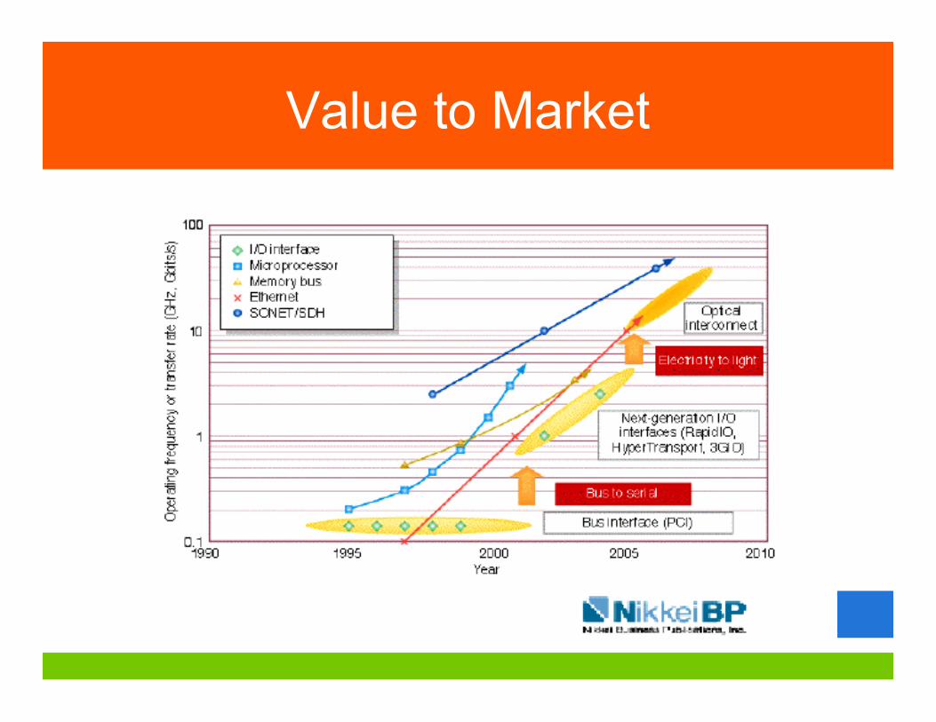
Value to Market

“Faster” Backplanes
• Making the copper thicker
• Making the dielectric layer thinner
• Using dielectrics with lower loss tangents
• Adding more signal layers
• Minimizing the signal length
• Maximizing distance between signals
• Making the board larger (wider and longer) tohandle more signals per layer

Copper Roadmap
Teradyne connectors HDM VHDM & VHDM L-series VHDM-HSD Gbk GBx
ERNI connectors ERmet Ermet Ermet ZD ERmetZD Ermet Zero XT
Tyco connectors HM-ZD Z-Pack HM-ZD Z-Pack HM-ZD
MultiGig RT-1 MultiGig RT-2 MultiGig RT-3
FCI Metral 2000 AirMax VS AirMax VS AirMax VS AirMax
Metral 4000
Fujitsu FCN-261Z00x FCN260D
Winchester Xcell SIP-1000 I platform
Molex Molex is a Teradyne licensee
Taps required
Velio GigaCore2
Shared Bus ?
Point to Point ?
Multi point ? Sub type?
Generic Copper Backplane Bandwidth Technology Roadmap
PTFE / Ceramic, Df = 0.002 - 0.0009FR-4, Df = 0.020 PPO / CE, Df = 0.015-0.008
BT / APPE, Df = 0.010
PTFE, Df = 0.009 - 0.003
1 Gbps ? 2.5 GBPS ? 3.125 Gbps ? 4.0 Gbps ? 6.125 Gbps ? 10 Gbps - 40Gbps
Materials
PCB Technology
Connector Launch Design
Transmission Line Design
Differential pair, length, type (Surface microstrip, embedded microstrip, stripline, edge coupled, broadside coupled), location in stack
Single transmission line, Length management
Processes
Standard processes Backdrilling ? Dual density drilling?
Bus Architecture
Receiver / Transmitter Signal Conditioning Chip
Set
Pad in via or PTH, micro vias, buried vias
Decrease PTH diameter, Remove non-functional pads, Increase anti-pad diameter (Clearance ring)
Connector Technology
Via Design
GigaCore
None Required One Two Multiple
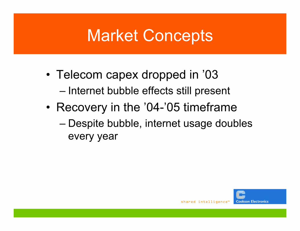
• Telecom capex dropped in ’03– Internet bubble effects still present
• Recovery in the ’04-’05 timeframe– Despite bubble, internet usage doubles
every year
Market Concepts
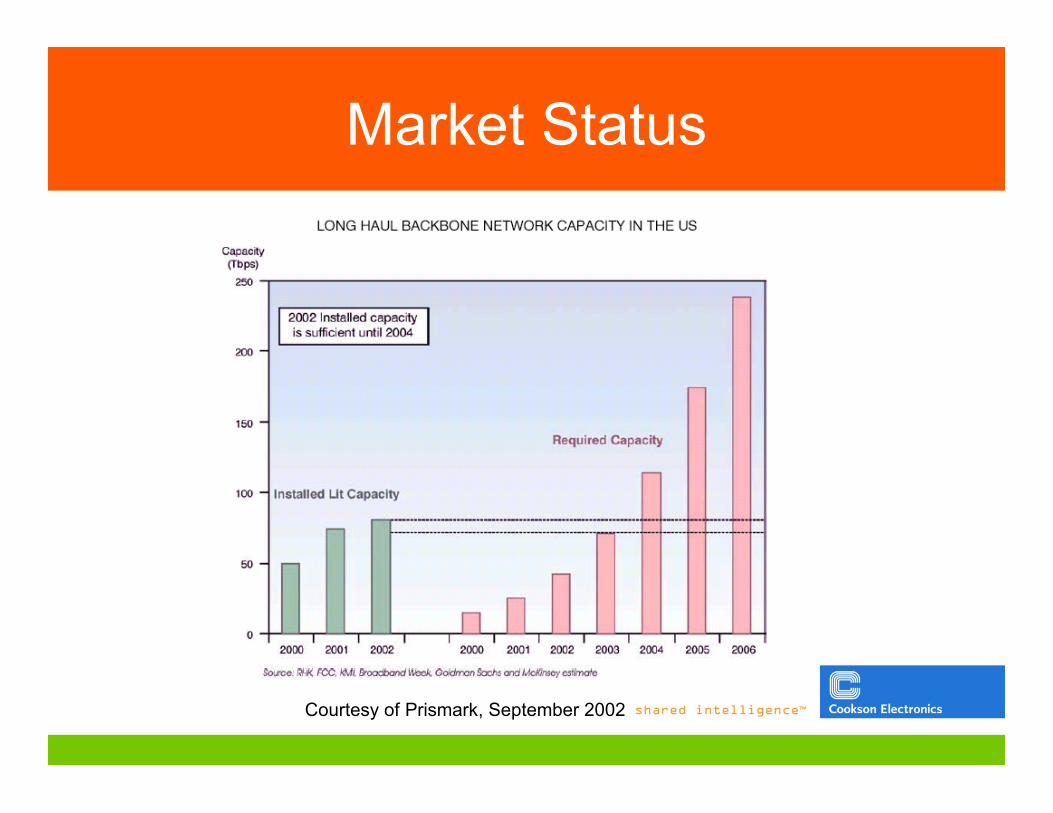
Courtesy of Prismark, September 2002
Market Status
Optical Backplanes
• Today: optical fibers / fiber mat on surface– Point-to-point limitation– Splice or connector required for each fiber end– Costly
• Future: planar optical waveguides– Patternable layer on or within PCB– Bus architecture– Laser/detector arrays “self-aligned” in assembly
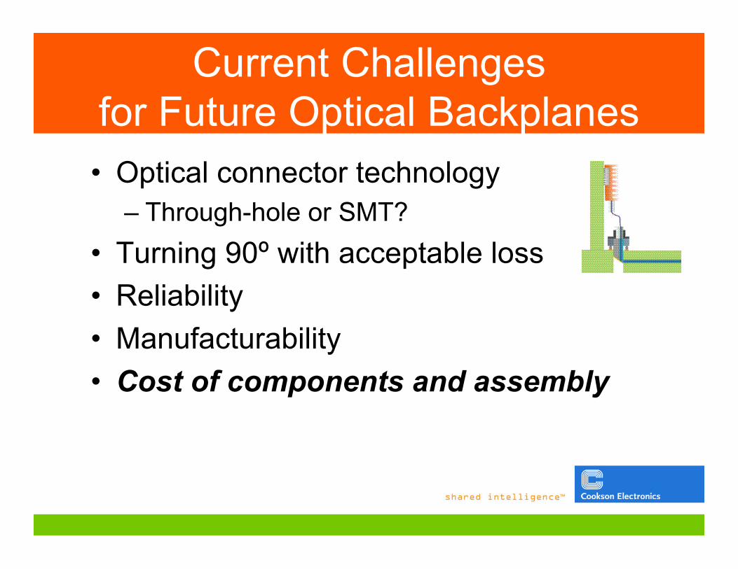
Current Challengesfor Future Optical Backplanes• Optical connector technology
– Through-hole or SMT?
• Turning 90º with acceptable loss
• Reliability
• Manufacturability
• Cost of components and assembly

The Cost Model
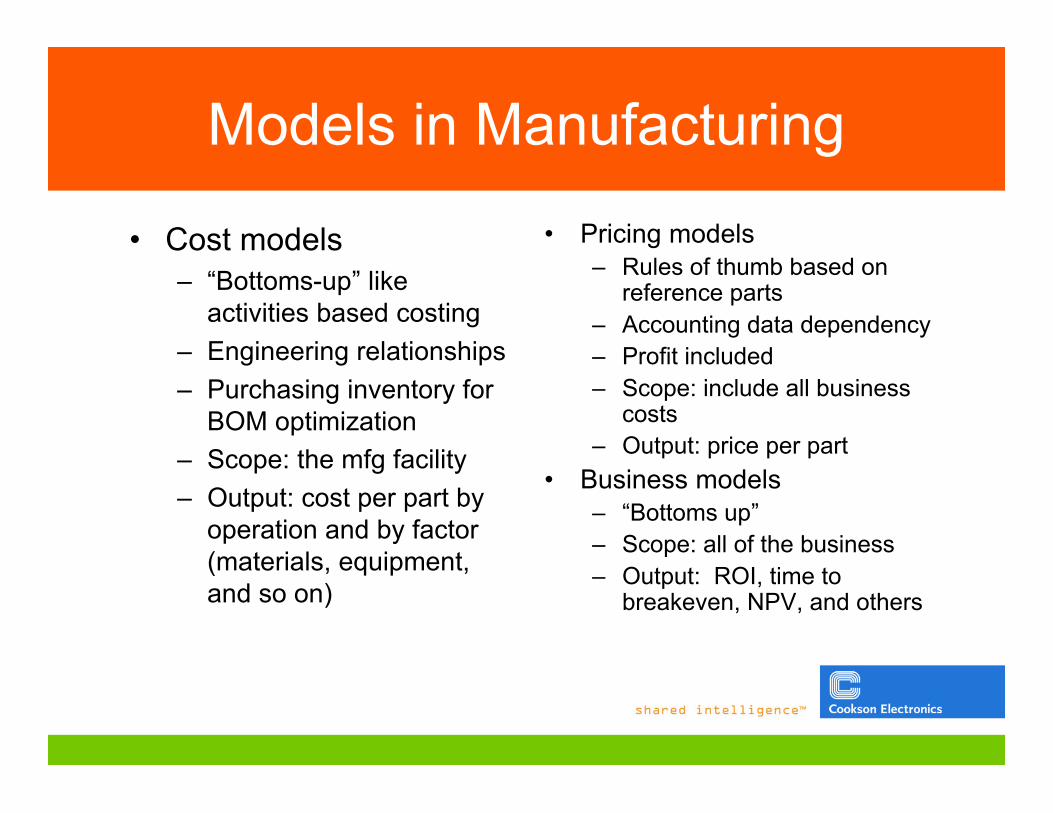
Models in Manufacturing
• Cost models– “Bottoms-up” like
activities based costing
– Engineering relationships
– Purchasing inventory forBOM optimization
– Scope: the mfg facility
– Output: cost per part byoperation and by factor(materials, equipment,and so on)
• Pricing models– Rules of thumb based on
reference parts– Accounting data dependency– Profit included– Scope: include all business
costs– Output: price per part
• Business models– “Bottoms up”– Scope: all of the business– Output: ROI, time to
breakeven, NPV, and others

Cost Modeling Method
• Based on Technical Cost Modeling, asdeveloped by IBIS Associates / MIT
• Activities Based Costing, plusengineering relationships– Cycle time = f(design, machine speed)
Design
Materials Processing
Design
Materials
MachineLimits
Cycle TimeCalculation
Equipment & Related
Inputs Cost output
Labor
Building
Utilities
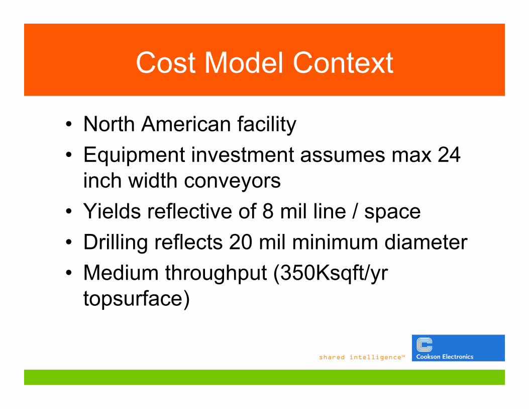
Cost Model Context
• North American facility
• Equipment investment assumes max 24inch width conveyors
• Yields reflective of 8 mil line / space
• Drilling reflects 20 mil minimum diameter
• Medium throughput (350Ksqft/yrtopsurface)

Facilities Assumptions
Direct Labor Wage $15.00 /hourIndirect Labor Salary $50,000 /year
Indirect Laborers:Direct Laborer Ratio 0.07 ilab/dlabIndirect Labor Shifts per Day 1.2 shift/day
Benefits on Wage/Salary 35.0%
Working Days per Year 360 d/yrWorking Hours per Day 24 h/d
Capital Recovery Rate 8% /yrWorking Capital Period 1 mo(s)
Equipment Depreciation Life 5 yrsBuilding Recovery Life 20 yrs
Total Space:Work Space Ratio 1.25 : 1Price of Electricity $0.110 /kWh
Dedicated Equipment? 0 [1=Y 0=N]
Equipment Investment Scaling Factor 100% of baseline
Non-Recurring Engineering $1,000 per design

Product Assumptions
• 32 metal layers
• No buried vias
• FR-4
• 24x20 inch panel
• 20x18 inch finished board
• 5,000 drilled holes per board
• ~1-3 Gbps performance

Process Flow
INNERLAYERRec1Cln1Pat1Pat2Pat3Pat4Pat5Pat6Pat7Ins1Prp1
Registration PunchAOIOxide Coating System
Photo PlotterDevelop Dry FilmEtch Cu - Strip ResistFilm Punch
Receive LaminateClean - ChemicalLaminate Dry FilmExpose Dry Film
OUTERLAYERLam1Lam2Lam3Lam4Lam5Lam6Drl1Drl2Drl4 DeburringDrl5 Auto Hole CheckDrl6 Desmear & Etchback - PMPlt1 Plate E'less CuPlt2 E'lytic Strike CuCln2 Clean - Pumice ScrubPat1 Laminate Dry FilmPat2 Expose Dry FilmPat3 Photo PlotterPat4 Develop Dry FilmPlt3 Plate E'lytic Cu & SnPat8 Strip Resist, Etch Cu, Strip SnDrl8 Manual Hole Size CheckIns1 AOIRep1 Repair Opens & ShortsCln1 Clean - ChemicalSma1 Flood Coat Solder Mask (DS Screening)Sma2 Tack CureSma3 Expose Solder MaskSma4 Develop Solder MaskSma5 UV CureSma6 CureHsl1 HASL & CleanNmn1 Nomenclature PrintFin1 Routing - DepanelingFin2 CleanIns2 Electrical TestIns3 Flying ProbeFin3 Find, Analyze, Repair, RetestIns4 Final Inspection & AuditFin2 CleanFin4 Final packaging & labelingWst1 Waste TreatmentNre1 Non-recurring Engineering
Deflash & IDPin Stack - Before DrillDrill Through Holes
Receive FoilKitting and Lay-up AreaLaminate Multilayer (Press)Routing - Depin and Debook
Receive Prepreg

Cost Summary
Cost Summary (per board)
Innerlayer Cost $416 74% $44.0 MMOuterlayer Cost $144 26% 23.0 K sqft
Total Cost $560 $2.1 MM
Cost/Sqin (Top Surface, Board) $1.55Cost/Sqin (Top Surface, Panel) $1.17
Cost/Sqin (Per Metal Layer) $0.036
Cost Factor Breakdown (per board)
Dir Labor Material Utilities Tooling Equip Bldg Ind Labor Maint CapitalInnerlayer Cost $86 $258 $2 $10 $34 $0 $9 $7 $10% of innerlayer 21% 62% 0% 2% 8% 0% 2% 2% 2%
Outerlayer Cost $33 $49 $1 $18 $25 $0 $5 $5 $7% of outerlayer 23% 34% 1% 13% 18% 0% 4% 4% 5%
Total Cost $119 $307 $3 $28 $59 $1 $14 $12 $17% of total 21% 55% 1% 5% 11% 0% 2% 2% 3%
Total Building Investment
Total Equipment InvestmentTotal Building Space
Validated by two backplane fabricators:+/- 10% of their costs

Cost Analysis
Cost perNo. of No. of Post Total Cost per Cost per Top Panel Total TotalDrilled Metal Lam'n Board Board Top Panel Surface Sqin Equipment BuildingHoles Layers Yield Cost Metal Layer Surface Sqin Metal Lyr Invest (MM) Space (Ksqft)
Baseline Case 5,000 32 88% $560 $17.49 $1.17 $0.036 $44 23.0
Holes Lower 2,500 32 88% $545 $17 $1.14 $0.036 $43 22.1Holes Higher 7,500 32 88% $574 $17.94 $1.20 $0.037 $45 24.2Holes Highest 10,000 32 88% $588 $18.39 $1.23 $0.038 $46 25.1
Layers Lower 5,000 24 91% $423 $17.61 $0.88 $0.037 $38 20.0Layers Higher 5,000 36 86% $634 $17.61 $1.32 $0.037 $47 24.4
Holes & Layers Lowest 2,500 24 91% $411 $17.14 $0.86 $0.036 $37 19.1Holes & Layers Highest 10,000 36 86% $668 $18.56 $1.39 $0.039 $49 26.5

“The Metric”
So far, cost has focused on board cost
But is that fair comparison for optical PCBs?– Performance will be at a different level– Connectors will be different– Assembly method probably different
So, what metric to use?

“The Metric”
• Cost per Gbps per top surface square inch: takes into account thenumber of metal layers (not including ground/power planes), maximumGbps per channel, and maximum channels per inch (as determined byminimum line/space rules)
• Cost per Gbps per channel per meter: takes into account losses perunit length and maximum Gbps per channel
• Cost per Gbps per board: takes into account design-dependentmaximum Gbps for all channels on the board at any one time
• Cost per Gbps per board cross-section: takes into accountmaximum Gbps per channel and the number of channels cut by across-section dividing the length of the board into equal parts
• Suggestions?
Crossover zone:changeover will not be
immediate, but will rangedepending on issues includingcost sensitivity, reliability, and
design limitations
Bandwidth x Distance
Rel
ativ
e C
ost Copper
PCB
Optical PCB
20042000

• Next generation copper PCB for 10Gbps
• Assembly costs
• Optical PCB technology– Embedded, edge-coupled
– Embedded, surface-coupled• Mirror/grating/in-via-coupling
• Bent waveguide
Future Work
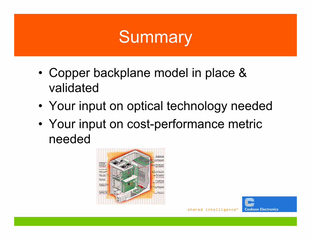
Summary
• Copper backplane model in place &validated
• Your input on optical technology needed
• Your input on cost-performance metricneeded