neuro-inspired processor design for on-chip … learning and classification with cmos and resistive...
TRANSCRIPT

1
Neuro-Inspired Processor Design for
On-Chip Learning and Classification
with CMOS and Resistive Synapses
Jae-sun Seo
School of ECEE, Arizona State University
The 13th Korea-U.S. Forum on Nanotechnology
September 26, 2016
2
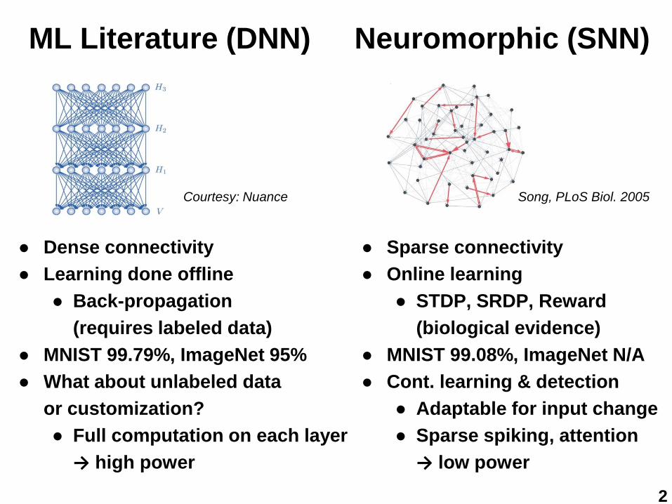
ML Literature (DNN) Neuromorphic (SNN)
Song, PLoS Biol. 2005 Courtesy: Nuance
● Dense connectivity
● Learning done offline
● Back-propagation
(requires labeled data)
● MNIST 99.79%, ImageNet 95%
● What about unlabeled data
or customization?
● Full computation on each layer
→ high power
● Sparse connectivity
● Online learning
● STDP, SRDP, Reward
(biological evidence)
● MNIST 99.08%, ImageNet N/A
● Cont. learning & detection
● Adaptable for input change
● Sparse spiking, attention
→ low power
3
2.05mm
2.0
5m
m
Base design Slim neuron
variant
4-b synapse
variantLow leakage
variant
64K
synapse
array
256K
synapse
array
64K
synapse
array
64K
synapse
array
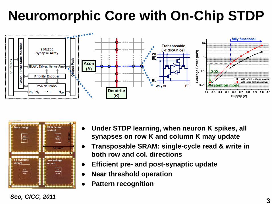
Neuromorphic Core with On-Chip STDP
● Under STDP learning, when neuron K spikes, all
synapses on row K and column K may update
● Transposable SRAM: single-cycle read & write in
both row and col. directions
● Efficient pre- and post-synaptic update
● Near threshold operation
● Pattern recognition
20X
fully functional
retention mode
Seo, CICC, 2011
4
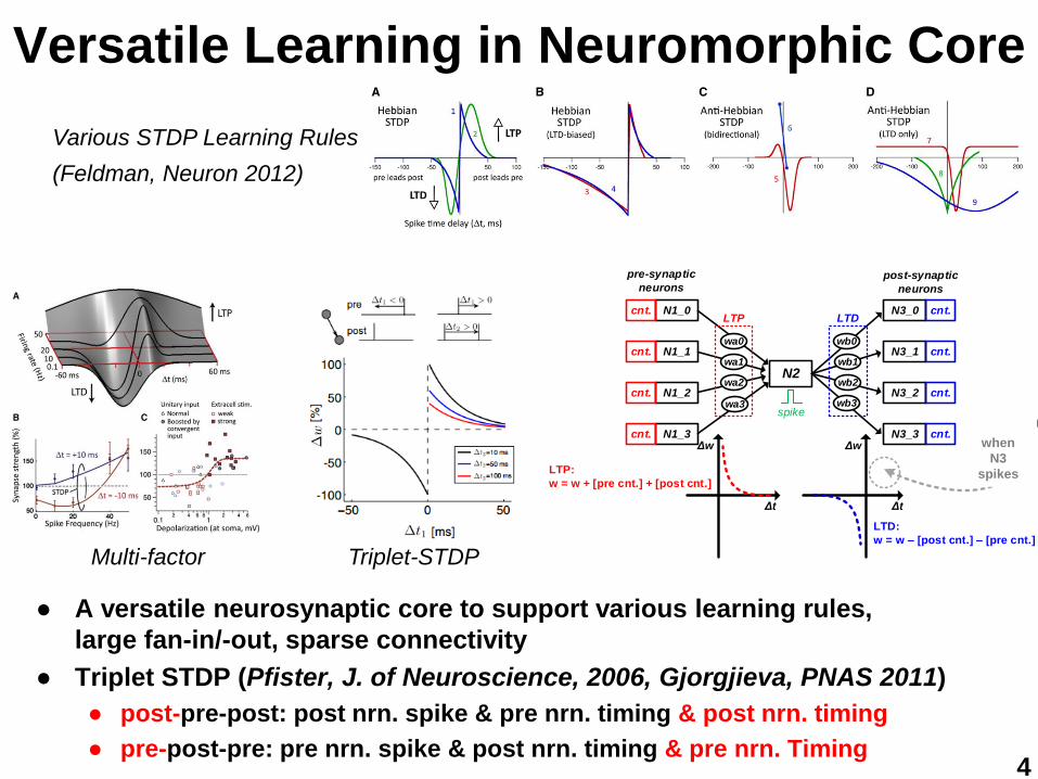
Versatile Learning in Neuromorphic Core
● A versatile neurosynaptic core to support various learning rules,
large fan-in/-out, sparse connectivity
● Triplet STDP (Pfister, J. of Neuroscience, 2006, Gjorgjieva, PNAS 2011)
● post-pre-post: post nrn. spike & pre nrn. timing & post nrn. timing
● pre-post-pre: pre nrn. spike & post nrn. timing & pre nrn. Timing
Various STDP Learning Rules
(Feldman, Neuron 2012)
Multi-factor Triplet-STDP
N2
N3_0
N3_1wb0
N3_2
N3_3
wb1
wb2
wb3
N1_0
N1_1wa0
N1_2
N1_3
wa1
wa2
wa3spike
LTDLTP
pre-synaptic
neuronspost-synaptic
neurons
cnt.
cnt.
cnt.
cnt.
cnt.
cnt.
cnt.
cnt.ΔwΔw
ΔtΔt
When N3 spikes,
wb* synapses are
subject to LTP
LTP:
w = w + [pre cnt.] + [post cnt.]
LTD:
w = w – [post cnt.] – [pre cnt.]
when
N3
spikes

5
de
co
de
r
A
xo
ns w
/ ti
min
g info
.
Synapse
Array
1024x256spike
packet
spike
packet
rec
urr
en
t c
on
nec
tio
n
Sy
na
ps
es
: T
X =
> In
hib
.
Inh.nrn
Synapses
Inh. => RX neuron
256 Neurons
spike timing info.
Layer (i) neurons
Layer (i+1) neurons
Inhibition
Feedforward Excitation & Inhibition
[1] Diehl, Front. of Neuroscience, 2015
● Joint feed-forward excitation and inhibition
● For a small number of inhibitory neurons,
add pre=>inh, inh=>post synapses
● Balance excitatory & inhibitory synaptic inputs
Vogels, Science, 2011
6
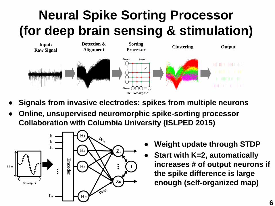
Neural Spike Sorting Processor
(for deep brain sensing & stimulation)
● Signals from invasive electrodes: spikes from multiple neurons
● Online, unsupervised neuromorphic spike-sorting processor
Collaboration with Columbia University (ISLPED 2015)
Input:
Raw Signal
Detection &
AlignmentClustering
Sorting
ProcessorOutput
neuromorphic
En
cod
er
H1
Z1
ZK
...H2
H3
HN
I...
I1
I2
I3
Im
8 bits
32 samples
● Weight update through STDP
● Start with K=2, automatically
increases # of output neurons if
the spike difference is large
enough (self-organized map)

7
Exp. Results: Clustering Accuracy
D2 D3 D4 D4* W-D1 W-D20
20
40
60
80
100
Accu
racy(%
)
Dataset
Proposed. Avg acc.= 91%
Osort based. Avg acc.=69%
Receptive field of dataset that contains 4 clusters in 3000 spikes
Spike sorting accuracy more
reliable than other low-complexity
algorithms such as O-sort
Avg. accuracy: 91% vs. 69%
Synapse
Array
Input
NeuronsOutput
Neurons
Output
Neurons
Others
Decoder
0.2 0.3 0.4 0.5 0.6 0.7 0.8 0.9 1.0 1.10.01
0.1
1
10
100
9.3W/ch
70 spikes/s/neuron ([4])
Fre
qu
en
cy(M
Hz)
VDD (V)
2.5 spikes/s/neuron
(D2, D3, D4, D4*)
26W/ch
• 65nm GP, high-Vth, 0.5x0.5mm2
• 9.3µW/ch at 0.3V
•Layout of the design is dominated by memory elements, as well as power.

8
Neuromorphic Computing w/ NVMs
● Emerging NVMs (e.g.
RRAM) could alleviate
power/area bottleneck
of conv. memories
● Read rows in parallel:
weighted sum current
● Peripheral CMOS read:
current-to-digital converter
130nm
RRAM array +
CMOS read circuits
(under testing)
0.50
0.53
0.0
1.5
1 2 3 4 5 6 7 8 1 2 3 4 5 6 7 8
RE RE
Vspike
Vspike
Vin
Vin
Time (ns)
Vo
ltag
e (
V)
Simulation results for 4ns read timing window

9
Summary
● Neuromorphic computing hardware
● 45nm testchip with on-chip STDP learning
● Versatile learning neuromorphic core & architecture
● 65nm spike clustering processor
● Emerging NVM arrays + peripheral read/write circuits
● Future research with circuit-device-architecture co-
design and optimization

10
Collaborators
● ASU
● Faculty: Yu Cao, Shimeng Yu, Chaitali Chakrabarti, Sarma
Vrudhula, Visar Berisha
● Students: Minkyu Kim, Deepak Kadetotad, Shihui Yin,
Abinash Mohanty, Yufei Ma
● Intel: Gregory Chen, Ram Krishnamurthy
● Columbia University: Mingoo Seok, Qi Wang