new approach to design a compact triband bandpass lter
TRANSCRIPT
Turk J Elec Eng & Comp Sci
(2017) 25: 4006 – 4012
c⃝ TUBITAK
doi:10.3906/elk-1609-129
Turkish Journal of Electrical Engineering & Computer Sciences
http :// journa l s . tub i tak .gov . t r/e lektr ik/
Research Article
New approach to design a compact triband bandpass filter using a multilayer
structure
Sohrab MAJIDIFAR1,∗, Mohsen HAYATI21Young Researchers and Elite Club, Kermanshah Branch, Islamic Azad University, Kermanshah, Iran
2Department of Electrical Engineering, Kermanshah Branch, Islamic Azad University, Kermanshah, Iran
Received: 14.09.2016 • Accepted/Published Online: 17.02.2017 • Final Version: 05.10.2017
Abstract: In this paper, a triband bandpass filter is presented using a dual-layer structure. Three H-shaped resonators
are utilized in the proposed structure. The first and third resonators are placed at the top and bottom layers, respectively.
The second resonator is divided into two parts: one half is on the top and the other half is at the bottom. The effective
permittivity at the first and second layers is different, resulting in different resonant frequencies. The fabricated triband
bandpass filter operates at 5.44/6.98/8.36 GHz, with fractional bandwidths of 6.6%/6%/2.9% and measured minimal
insertion losses of 1.9/1.7/2 dB.
Key words: Triband, multilayer structure, passband tuning
1. Introduction
Microstrip filters are in high demand in modern communication systems due to their significant features such
as compactness, planar structure, and ease of fabrication [1–21]. Multistandard communication systems require
multiband microwave filters. A variety of approaches to designing microstrip triband bandpass filters (BPF)
have been proposed [4–21]. Combining three single-band filters in parallel has been presented in [4]. In
this approach, each passband can be independently controlled, while the circuit size is not compact enough.
Asymmetric stepped-impedance resonators (SIRs) with only one discontinuity can also be used to construct
multiband BPFs with the merit of compact circuit size, low loss, and better design feasibility [5–8]. Creating a
transmission zero to split one passband of a dual-band BPF into two has been presented in another approach
[9]. This method achieves a controllable isolation between passbands, whereas the transition bands are not
sharp. Half-wavelength [10] and quarter-wavelength [11] SIRs have been utilized to design quadband or triband
BPFs. The trisection SIRs have been used to design triband filters in [12,13]. Another type of triband BPFs has
been designed using multimode resonators [14] such as stepped-impedance resonators or stub-loaded resonators
[15–18]. Using the higher modes of a dual-mode resonator has been reported in [19]. High performance and
compact size triband bandpass filters have been proposed using high-temperature superconducting structure
[20] and defected ground structure [21], respectively.
In this paper, a triband BPF is presented using a simple principle: different dielectric constant results
in different resonant frequencies. This hypothesis is tested by using a multilayer configuration. In order to
reduce the physical size and increase the isolation between passbands, the surface-coupling structure is modified
∗Correspondence: [email protected]
4006

MAJIDIFA and HAYATI/Turk J Elec Eng & Comp Sci
to coupling between the layers in the proposed dual-layer structure. Using the proposed structure has two
important advantages: reduction of physical size (almost 50%) and reduction of designer limitations through
access to the two substrates in a single structure. To validate the proposed method, a triband BPF prototype
has been designed, fabricated, and measured.
2. Filter design
The basic structure of the proposed triband bandpass filter and its simulation results are shown in Figures 1a and
1b, respectively. The dimensions of this structure, which is composed of three cascaded H-shaped resonators,
are as follows: a = 0.176 mm, b = 2.9 mm, c = 2.37 mm, d = 6.77 mm, e = 0.176 mm, h = 5.17 mm, i = 3 mm,
m = 1.17 mm, and n = 0.7 mm. The proposed structure was designed on RT/duroid 5880 with a dielectric
constant of 2.2 and a thickness of 0.381 mm. As illustrated in Figure 1b, the resonant frequencies of the basic
structure have been centered at 6.38 GHz, 6.88 GHz, and 7.4 GHz. There is no isolation between the passbands;
hence, passband control is not possible. Figure 2 shows the circuit model of the basic structure.
Figure 1. Basic structure of the proposed triband bandpass filter: a) layout, b) simulation results.
In this model, L i and C i are inductance and capacitance of input and output ports, respectively. C1 and
C2 introduce the body capacitance of the vertical lines in the H-shape resonator. Cg is the coupling capacitance
between vertical lines and L1 shows the inductance of the horizontal line in the H-shape resonator. Using Eqs.
(1)–(5) and certain optimization [2], these circuit parameters are calculated as follows: L i = 1 nH, C i = 0.61
4007

MAJIDIFA and HAYATI/Turk J Elec Eng & Comp Sci
Figure 2. Circuit model of the basic structure.
pF, L1 = 3.87 nH, C1 = 0.12 pF, C2 = 0.11 pF, and Cg = 0.073 pF.
C = [8.85(10)−12[εrwh
]1.08 + [2π(εr + 1
2)(
1
ln( 8hw + 1)− w
8h)]1.080.926]l (1)
L =lzcvp
(2)
vp =c
√εre
(3)
For w/h ≤ 1
εre =εr + 1
2+
εr − 1
2[1 + 12
h
w]−0.5 + 0.04[1− w
h]2, zc =
η
2π√εre
ln[8h
w+ 0.25
w
h] (4)
For w/h ≥ 1
εre =εr + 1
2+
εr − 1
2[1 + 12
h
w]−0.5, zc =
η√εre
wh
+ 1.393 + 0.677 ln[w
h+ 1.444]−1, (5)
where the equivalent capacitance and inductance of the resonator parts are introduced by C and L, zc and vp
characteristics impedance and phase velocity, respectively, w, l, h, and εre are line width, line length, substrate
thickness, and effective permittivity, respectively, η is a constant equal to 120πΩ, and c represents the light
speed.
Figure 3 shows the EM and circuit simulation results of the basic structure and its model. As shown in
Figure 3, this result is well matched with the EM simulation results.
To control the passbands and increase the isolation between them, a dual layer structure is used. In this
method, the proposed basic structure in Figure 1a is divided into two parts. The first resonator and half of
the second resonator remain unchanged on the top layer. The next half of the second resonator and the third
resonator are displaced from the top to the bottom layer, while the back of the bottom layer is metalized as
the ground plane. The input/output ports are assembled between the top layer/bottom layer and the ground
plane. The substrate thickness of the first resonator is double of a single layer and its effective permittivity is
1.7, while the effective permittivity of the third resonator is 2.2. Two parts of the second resonator, which are
designed on the top and bottom layers, are connected through a via hole and resonate between the resonant
frequencies of the first and third resonators.
4008

MAJIDIFA and HAYATI/Turk J Elec Eng & Comp Sci
Figure 3. EM and circuit simulation results of the basic structure and its model.
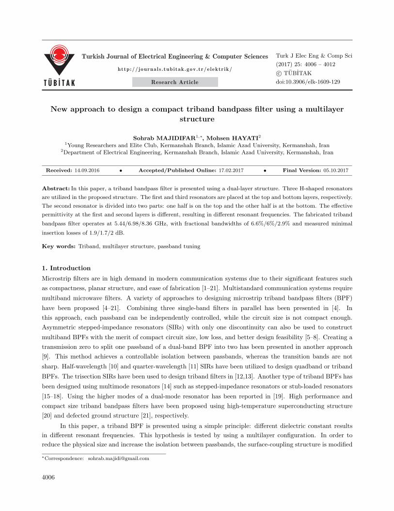
Figures 4a and 4b show the layout and simulation results of the proposed filter. As illustrated in Figure
4a, the dimensions of the resonators on the bottom layer have been scaled to control the passband frequencies.
Input and output lines are designed on both sides of the filter to be connected to 50-Ω SMA. The resonant
frequencies of the filter appear at 5.33 GHz, 6.88 GHz, and 8.27 GHz. The first passband is created by the third
resonator on the bottom layer due to increasing the scale of the third resonator, while the associated effective
dielectric constant remains unchanged and equals 2.2.
The second band is related to the second resonator, whose two parts (on the top and bottom layer) are
connected with a via hole. The third band is created by the first resonator on the top layer, where the effective
dielectric constant is no longer 2.2, but has changed to 1.7. This smaller effective permittivity shifts the resonant
frequency to higher frequencies. Hence, three fully tunable passbands are realized.
To improve passband isolation, two deep transmission zeros have been located at 6.07 GHz and 7.58 GHz
with magnitudes of –35 dB and –42 dB, respectively. Two out-of-band transmission zeros at 4.75 GHz and 8.68
GHz have been generated to realize sharp passband skirt performance. The simulation results of the proposed
filter in terms of insertion loss, return loss, and sharpness are shown in Table 1. Total size of the fabricated filter
without feed lines is 0.34 λg× 0.16 λg , where λg is the guided wavelength of the first passband. A comparison
between the total size of the filters (both in this work and in those reported in the introduction) is shown in
Table 2.
Table 1. Passbands specifications of the designed filter.
Passband Insertion Return Sharpness of the first/second transition
loss (dB) loss (dB) band of each passband (dB/GHz)
First 0.32 15 58.62/37.78
Second 0.39 16.65 36.17/43.59
Third 0.52 22.4 34.69/85
Table 2. Comparison between the total size of the filters.
Ref. no. [4] [7] [9] [11] [12] [13] [14]
Total size (λg × λg) 0.32 × 0.49 0.33 × 0.25 0.181 × 0.176 0.108 × 0.521 0.195 × 0.195 0.24 × 0.22 0.16 × 0.17
Ref. no. [15] [16] [17] [18] [20] [21] This work
Total size (λg × λg) 0.26 × 0.13 0.17 × 0.15 0.26 × 0.22 0.18 × 0.38 0.066 × 0.051 0.14 × 0.22 0.16 × 0.34
4009
MAJIDIFA and HAYATI/Turk J Elec Eng & Comp Sci
Figure 4. Proposed triband bandpass filter: a) layout, b) simulation results.
3. Fabrication and measurement
Figure 5 shows the pictures of the top layer, bottom layer, and final filter structure. The measurement and
simulation results of the filter are shown in Figure 6. The triband BPF operates at 5.44/6.98/8.36 GHz, with
fractional bandwidths of 6.6%/6%/2.9% and measured minimal insertion losses of 1.2/1.7/2 dB. Compared to
the simulation result, the measurement result shows a 110-MHz, 100-MHz, and 90-MHz frequency shift for the
first, second, and third passbands, respectively. This shift is mainly due to the gap between the two connected
layers (top and bottom layer), which is neglected in the simulation.
4010

MAJIDIFA and HAYATI/Turk J Elec Eng & Comp Sci
Figure 5. Pictures of the fabricated filter.
Figure 6. Simulation and measurement results of the proposed filter.
4. Conclusion
A compact adjustable triband bandpass filter is presented in this paper. In the presented approach, two stacked
layers of substrate are used to introduce two different effective permittivities to control the multiple resonant
frequencies. In this structure, each band can be independently controlled, which makes the proposed triband
filter suitable for multiband wireless communication systems.
4011

MAJIDIFA and HAYATI/Turk J Elec Eng & Comp Sci
References
[1] Demirel S, Uyank C. Design and analysis of a novel UWB bandpass filter using 3-D EM simulation-based neural
network model with HSA. Turk J Elec Eng & Comp Sci 2016; 3: 656-668.
[2] Majidifar S. High performance microstrip LPFs using dual taper loaded resonator. Optik 2016; 127: 3484-3488.
[3] Majidifar S. Design of high performance miniaturized lowpass filter using new approach of modeling. Appl Comput
Electrom 2016; 31: 52-57.
[4] Song F, Wei B, Zhu L, Feng Y, Wang R, Cao B. A novel tri-band superconducting filter using embedded stub-loaded
resonators. IEEE T Appl Supercon 2016; 26: 1502009.
[5] Chang YC, Kao CH, Weng MH, Yang RY. Design of the compact dual-band bandpass filter with high isolation for
GPS/WLAN applications. IEEE Microw Wirel Co 2009; 19: 780-782.
[6] Wu HW, Yang RY. A new quad-band bandpass filter using asymmetric stepped impedance resonators. IEEE Microw
Wirel Co 2011; 21: 203-205.
[7] Chen WY, Weng MH, Chang SJ, Kuan H, Su YH. A new tri-band bandpass filter for GSM, WiMAX and ultra-
wideband responses by using asymmetric stepped impedance resonators. Prog Electromagn Res 2012; 124: 365-381.
[8] Weng MH, Kao CH, Chang YC. A compact dual-band bandpass filter with high band selectivity using cross-coupled
asymmetric SIRs for WLANs. J Electromagnet Wave 2010; 24: 161-168.
[9] Ren LY. Tri-band bandpass ?lters based on dual-plane microstrip/DGS slot structure. IEEE Microw Wirel Co 2010;
20: 429-431.
[10] Yang CF, Chen YC, Kung CY, Lin JJ, Sun TP. Design and fabrication of a compact quad-band bandpass filter
using two different parallel positioned resonators. Prog Electromagn Res 2011; 115: 159-172.
[11] Zhang S, Zhu L. Compact tri-band bandpass filter based on λ/4 resonators with U- folded coupled-line. IEEE
Microw Wirel Co 2013; 23: 258-260.
[12] Chu QX, Lin XM. Advanced triple-band bandpass filter using tri-section SIR. Electron Lett 2008; 44: 295-296.
[13] Chen FC, Chu QX. Compact triple-band bandpass filter using pseudo interdigital trisection stepped impedance
resonators. Microw Opt Techn Let 2008; 50: 2462-2465.
[14] Li Q, Zhang YH, Feng X, Fan Y. Tri-band filter with multiple transmission zeros and controllable bandwidths. Int
J Microw Wirel Technol 2016; 8: 9-13.
[15] Lan SW, Wen MH, Chang SJ, Hung CY, Liu SK. A tri-band bandpass filter with wide stopband using asymmetric
stub-loaded resonators. IEEE Microw Wirel Co 2015; 25: 19-21.
[16] Wei F, Qin PY, Guo YJ, Shi XW. Design of multi-band bandpass filters based on stub loaded stepped-impedance
resonator with defected microstrip structure. IET Microw Antenna P 2015; 10: 1-7.
[17] Wu Q, Cui H, Sun P, Sun H, Sun X. On-chip tri-band bandpass filters using square ring open-stub loaded resonator
on GaAs substrate. Microw Opt Technol Lett 2016; 58: 1958-1961.
[18] Wei F, Guo YJ, Qin PY, Shi XW. Compact balanced dual- and tri-band bandpass filters based on stub loaded
resonators. IEEE Microw Wirel Co 2015; 25: 76-78.
[19] Luo S, Zhu L, Sun S. Compact dual-mode triple-band bandpass ?lters using three pairs of degenerate modes in a
ring resonator. IEEE T Microw Theory 2011; 59: 1222-1229.
[20] Liu H, Ren B, Zhan X, Guan X, Wen P, Zhu S, Peng Y, Ma Z. Tri-band high-temperature superconducting bandpass
filters using multimode resonators. IEEE T Microw Theory 2016; 26: 1501506.
[21] Wei F, Qin PY, Guo YJ, Ding C, Shi XW. Compact balanced dual- and tri-band BPFs based on coupled
complementary split-ring resonators (C-CSRR). IEEE Microw Wirel Co 2016; 26: 107-109.
4012