ni 6356 device specifications - national instruments · modes analog edge triggering, analog edge...
TRANSCRIPT
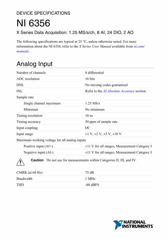
DEVICE SPECIFICATIONS
NI 6356X Series Data Acquisition: 1.25 MS/s/ch, 8 AI, 24 DIO, 2 AO
The following specifications are typical at 25 °C, unless otherwise noted. For moreinformation about the NI 6356, refer to the X Series User Manual available from ni.com/manuals.
Analog InputNumber of channels 8 differential
ADC resolution 16 bits
DNL No missing codes guaranteed
INL Refer to the AI Absolute Accuracy section.
Sample rate
Single channel maximum 1.25 MS/s
Minimum No minimum
Timing resolution 10 ns
Timing accuracy 50 ppm of sample rate
Input coupling DC
Input range ±1 V, ±2 V, ±5 V, ±10 V
Maximum working voltage for all analog inputs
Positive input (AI+) ±11 V for all ranges, Measurement Category I
Negative input (AI-) ±11 V for all ranges, Measurement Category I
Caution Do not use for measurements within Categories II, III, and IV.
CMRR (at 60 Hz) 75 dB
Bandwidth 1 MHz
THD -80 dBFS
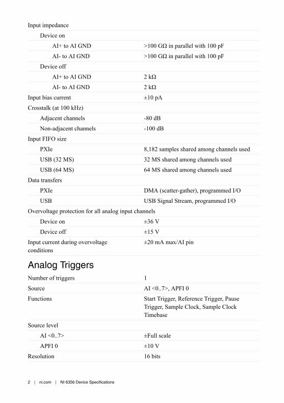
Input impedance
Device on
AI+ to AI GND >100 GΩ in parallel with 100 pF
AI- to AI GND >100 GΩ in parallel with 100 pF
Device off
AI+ to AI GND 2 kΩ
AI- to AI GND 2 kΩ
Input bias current ±10 pA
Crosstalk (at 100 kHz)
Adjacent channels -80 dB
Non-adjacent channels -100 dB
Input FIFO size
PXIe 8,182 samples shared among channels used
USB (32 MS) 32 MS shared among channels used
USB (64 MS) 64 MS shared among channels used
Data transfers
PXIe DMA (scatter-gather), programmed I/O
USB USB Signal Stream, programmed I/O
Overvoltage protection for all analog input channels
Device on ±36 V
Device off ±15 V
Input current during overvoltageconditions
±20 mA max/AI pin
Analog TriggersNumber of triggers 1
Source AI <0..7>, APFI 0
Functions Start Trigger, Reference Trigger, PauseTrigger, Sample Clock, Sample ClockTimebase
Source level
AI <0..7> ±Full scale
APFI 0 ±10 V
Resolution 16 bits
2 | ni.com | NI 6356 Device Specifications
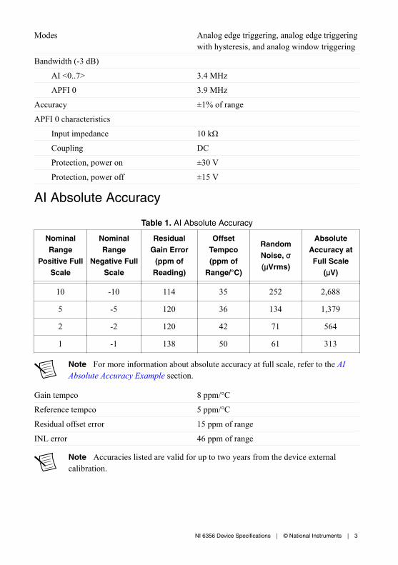
Modes Analog edge triggering, analog edge triggeringwith hysteresis, and analog window triggering
Bandwidth (-3 dB)
AI <0..7> 3.4 MHz
APFI 0 3.9 MHz
Accuracy ±1% of range
APFI 0 characteristics
Input impedance 10 kΩ
Coupling DC
Protection, power on ±30 V
Protection, power off ±15 V
AI Absolute Accuracy
Table 1. AI Absolute Accuracy
NominalRange
Positive FullScale
NominalRange
Negative FullScale
ResidualGain Error
(ppm ofReading)
OffsetTempco(ppm of
Range/°C)
RandomNoise, σ(μVrms)
AbsoluteAccuracy atFull Scale
(μV)
10 -10 114 35 252 2,688
5 -5 120 36 134 1,379
2 -2 120 42 71 564
1 -1 138 50 61 313
Note For more information about absolute accuracy at full scale, refer to the AIAbsolute Accuracy Example section.
Gain tempco 8 ppm/°C
Reference tempco 5 ppm/°C
Residual offset error 15 ppm of range
INL error 46 ppm of range
Note Accuracies listed are valid for up to two years from the device externalcalibration.
NI 6356 Device Specifications | © National Instruments | 3
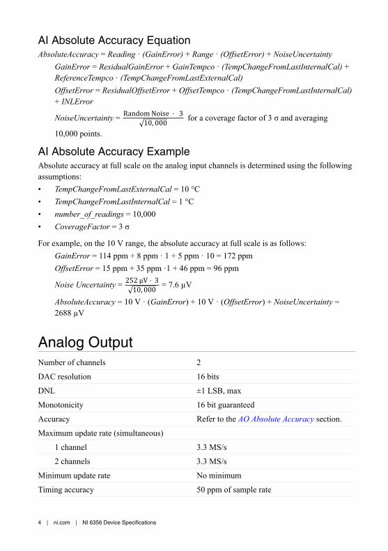
AI Absolute Accuracy EquationAbsoluteAccuracy = Reading · (GainError) + Range · (OffsetError) + NoiseUncertainty
GainError = ResidualGainError + GainTempco · (TempChangeFromLastInternalCal) +ReferenceTempco · (TempChangeFromLastExternalCal)OffsetError = ResidualOffsetError + OffsetTempco · (TempChangeFromLastInternalCal)+ INLError
NoiseUncertainty = RandomNoise ⋅ 310, 000 for a coverage factor of 3 σ and averaging
10,000 points.
AI Absolute Accuracy ExampleAbsolute accuracy at full scale on the analog input channels is determined using the followingassumptions:• TempChangeFromLastExternalCal = 10 °C• TempChangeFromLastInternalCal = 1 °C• number_of_readings = 10,000• CoverageFactor = 3 σ
For example, on the 10 V range, the absolute accuracy at full scale is as follows:GainError = 114 ppm + 8 ppm · 1 + 5 ppm · 10 = 172 ppmOffsetError = 15 ppm + 35 ppm ·1 + 46 ppm = 96 ppm
Noise Uncertainty = 252 μV ⋅ 310, 000 = 7.6 µV
AbsoluteAccuracy = 10 V · (GainError) + 10 V · (OffsetError) + NoiseUncertainty =2688 µV
Analog OutputNumber of channels 2
DAC resolution 16 bits
DNL ±1 LSB, max
Monotonicity 16 bit guaranteed
Accuracy Refer to the AO Absolute Accuracy section.
Maximum update rate (simultaneous)
1 channel 3.3 MS/s
2 channels 3.3 MS/s
Minimum update rate No minimum
Timing accuracy 50 ppm of sample rate
4 | ni.com | NI 6356 Device Specifications
Timing resolution 10 ns
Output range ±10 V, ±5 V, ±external reference on APFI 0
Output coupling DC
Output impedance 0.4 Ω
Output current drive ±5 mA
Overdrive protection ±25 V
Overdrive current 10 mA
Power-on state ±5 mV
Power on/off glitch
PXIe 1.5 V peak for 200 ms
USB 1.5 V peak for 200 ms, typical behavior1
Output FIFO size 8,191 samples shared among channels used
Data transfers
PXIe DMA (scatter-gather), programmed I/O
USB USB Signal Stream, programmed I/O
AO waveform modes Non-periodic waveform, periodic waveformregeneration mode from onboard FIFO,periodic waveform regeneration from hostbuffer including dynamic update
Settling time, full-scale step,15 ppm (1 LSB)
2 µs
Slew rate 20 V/µs
Glitch energy at midscale transition,±10 V range
6 nV · s
External ReferenceAPFI 0 characteristics
Input impedance 10 kΩ
Coupling DC
Protection, device on ±30 V
Protection, device off ± 15 V
1 Time period may be longer due to host system USB performance. Time period will be longerduring firmware updates.
NI 6356 Device Specifications | © National Instruments | 5
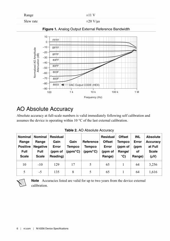
Range ±11 V
Slew rate ±20 V/μs
Figure 1. Analog Output External Reference Bandwidth
–90
–80
–70
–60
–50
–40
–30
–20
–10
0
10
100 1 k 10 k 100 k 1 M
Frequency (Hz)
Nor
mal
ized
AO
Am
plitu
deA
ttenu
atio
n (d
B)
DAC Output CODE (HEX)
FFFF
BFFF
8FFF
83FF
80FF
803F
800F
8003
AO Absolute AccuracyAbsolute accuracy at full-scale numbers is valid immediately following self calibration andassumes the device is operating within 10 °C of the last external calibration.
Table 2. AO Absolute Accuracy
NominalRange
PositiveFull
Scale
NominalRange
NegativeFull
Scale
ResidualGainError
(ppm ofReading)
GainTempco(ppm/°C)
ReferenceTempco(ppm/°C)
ResidualOffsetError
(ppm ofRange)
OffsetTempco(ppm ofRange/
°C)
INLError(ppm
ofRange)
AbsoluteAccuracy
at FullScale(μV)
10 -10 129 17 5 65 1 64 3,256
5 -5 135 8 5 65 1 64 1,616
Note Accuracies listed are valid for up to two years from the device externalcalibration.
6 | ni.com | NI 6356 Device Specifications
Digital I/O/PFI
Static CharacteristicsNumber of channels 24 total, 8 (P0.<0..7>),
16 (PFI <0..7>/P1, PFI <8..15>/P2)
Ground reference D GND
Direction control Each terminal individually programmable asinput or output
Pull-down resistor 50 kΩ typical, 20 kΩ minimum
Input voltage protection ±20 V on up to two pins
Caution Stresses beyond those listed under the Input voltage protectionspecification may cause permanent damage to the device.
Waveform Characteristics (Port 0 Only)Terminals used Port 0 (P0.<0..7>)
Port/sample size Up to 8 bits
Waveform generation (DO) FIFO 2,047 samples
Waveform acquisition (DI) FIFO 255 samples
DI Sample Clock frequency
PXIe 0 to 10 MHz, system and bus activitydependent
USB 0 to 1 MHz, system and bus activity dependent
DO Sample Clock frequency
PXIe
Regenerate from FIFO 0 to 10 MHz
Streaming from memory 0 to 10 MHz, system and bus activitydependent
USB
Regenerate from FIFO 0 to 10 MHz
Streaming from memory 0 to 1 MHz, system and bus activity dependent
Data transfers
PXIe DMA (scatter-gather), programmed I/O
USB USB Signal Stream, programmed I/O
Digital line filter settings 160 ns, 10.24 μs, 5.12 ms, disable
NI 6356 Device Specifications | © National Instruments | 7
PFI/Port 1/Port 2 FunctionalityFunctionality Static digital input, static digital output, timing
input, timing output
Timing output sources Many AI, AO, counter, DI, DO timing signals
Debounce filter settings 90 ns, 5.12 µs, 2.56 ms, custom interval,disable; programmable high and lowtransitions; selectable per input
Recommended Operating ConditionsInput high voltage (VIH)
Minimum 2.2 V
Maximum 5.25 V
Input low voltage (VIL)
Minimum 0 V
Maximum 0.8 V
Output high current (IOH)
P0.<0..7> -24 mA maximum
PFI <0..15>/P1/P2 -16 mA maximum
Output low current (IOL)
P0.<0..7> 24 mA maximum
PFI <0..15>/P1/P2 16 mA maximum
Digital I/O CharacteristicsPositive-going threshold (VT+) 2.2 V maximum
Negative-going threshold (VT-) 0.8 V minimum
Delta VT hysteresis (VT+ - VT-) 0.2 V minimum
IIL input low current (VIN = 0 V) -10 μA maximum
IIH input high current (VIN = 5 V) 250 μA maximum
8 | ni.com | NI 6356 Device Specifications
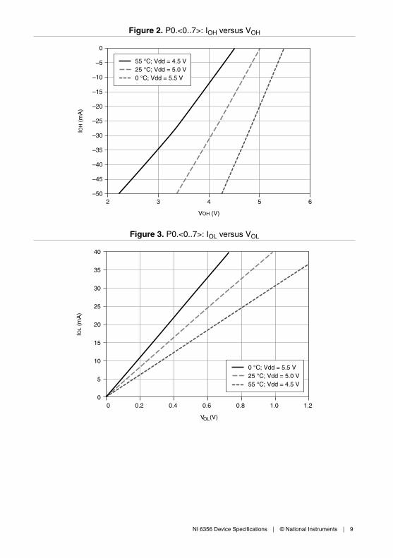
Figure 2. P0.<0..7>: IOH versus VOH
IOH
(m
A)
–30
–5
–10
–15
–20
–25
–35
–40
–45
VOH (V)
0
–50
55 °C; Vdd = 4.5 V25 °C; Vdd = 5.0 V0 °C; Vdd = 5.5 V
62 3 4 5
Figure 3. P0.<0..7>: IOL versus VOL
1.0
IOL
(mA
)
1.2
15
35
30
25
20
10
5
0 0.40.2 0.6 0.8
VOL (V)
40
0
0 °C; Vdd = 5.5 V25 °C; Vdd = 5.0 V55 °C; Vdd = 4.5 V
NI 6356 Device Specifications | © National Instruments | 9
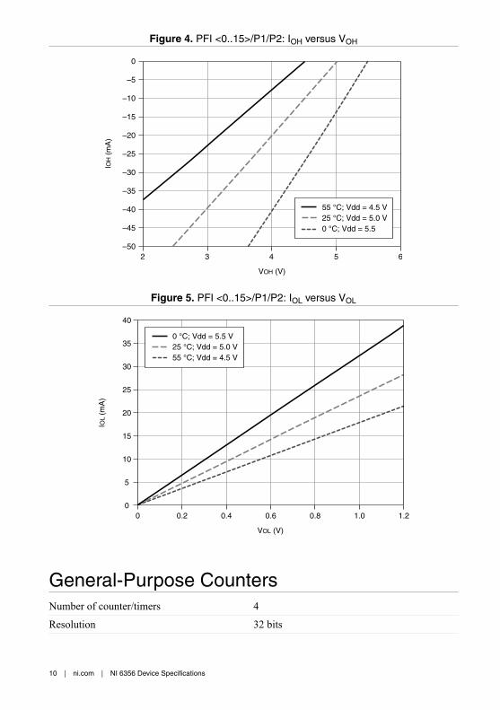
Figure 4. PFI <0..15>/P1/P2: IOH versus VOH
5
IOH
(m
A)
–30
–5
–10
–15
–20
–25
–35
–40
–45
2 3 4
VOH (V)
0
–506
55 °C; Vdd = 4.5 V25 °C; Vdd = 5.0 V0 °C; Vdd = 5.5
Figure 5. PFI <0..15>/P1/P2: IOL versus VOL
1.0
IOL
(mA
)
1.2
15
35
30
25
20
10
5
0 0.40.2 0.6 0.8
VOL (V)
0
0 °C; Vdd = 5.5 V25 °C; Vdd = 5.0 V55 °C; Vdd = 4.5 V
40
General-Purpose CountersNumber of counter/timers 4
Resolution 32 bits
10 | ni.com | NI 6356 Device Specifications
Counter measurements Edge counting, pulse, pulse width,semi-period, period, two-edge separation
Position measurements X1, X2, X4 quadrature encoding withChannel Z reloading; two-pulse encoding
Output applications Pulse, pulse train with dynamic updates,frequency division, equivalent time sampling
Internal base clocks 100 MHz, 20 MHz, 100 kHz
External base clock frequency
PXIe 0 MHz to 25 MHz; 0 MHz to 100 MHz onPXIe_DSTAR<A,B>
USB 0 MHz to 25 MHz
Base clock accuracy 50 ppm
Inputs Gate, Source, HW_Arm, Aux, A, B, Z,Up_Down, Sample Clock
Routing options for inputs
PXIe Any PFI, PXIe_DSTAR<A,B>, PXI_TRIG,PXI_STAR, analog trigger, many internalsignals
USB Any PFI, analog trigger, many internal signals
FIFO 127 samples per counter
Data transfers
PXIe Dedicated scatter-gather DMA controller foreach counter/timer, programmed I/O
USB USB Signal Stream, programmed I/O
Frequency GeneratorNumber of channels 1
Base clocks 20 MHz, 10 MHz, 100 kHz
Divisors 1 to 16
Base clock accuracy 50 ppm
Output can be available on any PFI terminal.
Phase-Locked Loop (PLL)Number of PLLs 1
NI 6356 Device Specifications | © National Instruments | 11
Table 3. Reference Clock Locking Frequencies
Reference Signal PXI Express Locking InputFrequency (MHz)
USB Locking InputFrequency (MHz)
PXIe_DSTAR<A,B> 10, 20, 100 —
PXI_STAR 10, 20 —
PXIe_CLK100 100 —
PXI_TRIG <0..7> 10, 20 —
PFI <0..15> 10, 20 10
Output of PLL 100 MHz Timebase; other signals derived from100 MHz Timebase including 20 MHz and100 kHz Timebases
External Digital TriggersSource
PXIe Any PFI, PXIe_DSTAR<A,B>, PXI_TRIG,PXI_STAR
USB Any PFI
Polarity Software-selectable for most signals
Analog input function Start Trigger, Reference Trigger, PauseTrigger, Sample Clock, Sample ClockTimebase
Analog output function Start Trigger, Pause Trigger, Sample Clock,Sample Clock Timebase
Counter/timer functions Gate, Source, HW_Arm, Aux, A, B, Z,Up_Down, Sample Clock
Digital waveform generation (DO)function
Start Trigger, Pause Trigger, Sample Clock,Sample Clock Timebase
Digital waveform acquisition (DI)function
Start Trigger, Reference Trigger, PauseTrigger, Sample Clock, Sample ClockTimebase
12 | ni.com | NI 6356 Device Specifications
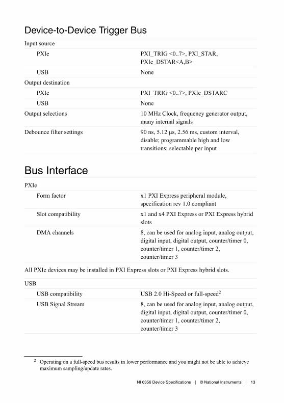
Device-to-Device Trigger BusInput source
PXIe PXI_TRIG <0..7>, PXI_STAR,PXIe_DSTAR<A,B>
USB None
Output destination
PXIe PXI_TRIG <0..7>, PXIe_DSTARC
USB None
Output selections 10 MHz Clock, frequency generator output,many internal signals
Debounce filter settings 90 ns, 5.12 μs, 2.56 ms, custom interval,disable; programmable high and lowtransitions; selectable per input
Bus InterfacePXIe
Form factor x1 PXI Express peripheral module,specification rev 1.0 compliant
Slot compatibility x1 and x4 PXI Express or PXI Express hybridslots
DMA channels 8, can be used for analog input, analog output,digital input, digital output, counter/timer 0,counter/timer 1, counter/timer 2,counter/timer 3
All PXIe devices may be installed in PXI Express slots or PXI Express hybrid slots.
USB
USB compatibility USB 2.0 Hi-Speed or full-speed2
USB Signal Stream 8, can be used for analog input, analog output,digital input, digital output, counter/timer 0,counter/timer 1, counter/timer 2,counter/timer 3
2 Operating on a full-speed bus results in lower performance and you might not be able to achievemaximum sampling/update rates.
NI 6356 Device Specifications | © National Instruments | 13
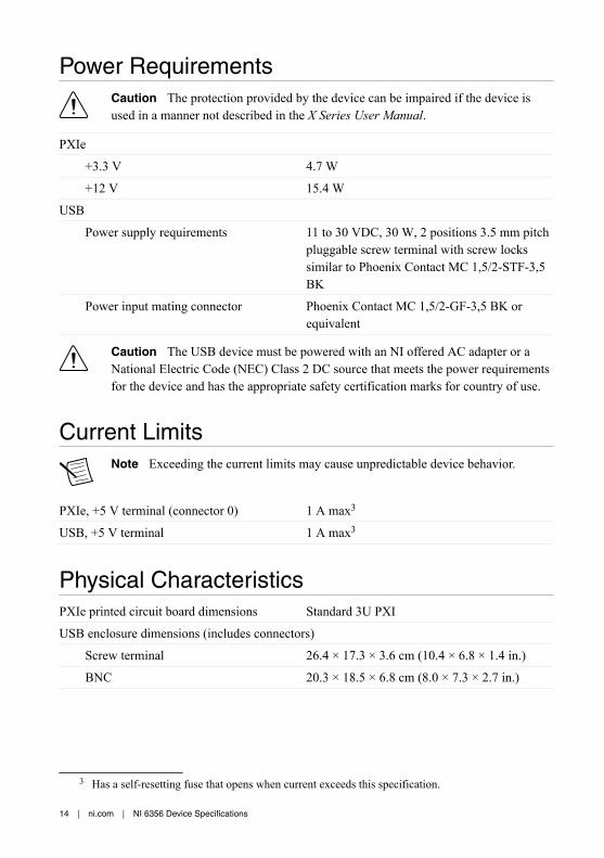
Power RequirementsCaution The protection provided by the device can be impaired if the device isused in a manner not described in the X Series User Manual.
PXIe
+3.3 V 4.7 W
+12 V 15.4 W
USB
Power supply requirements 11 to 30 VDC, 30 W, 2 positions 3.5 mm pitchpluggable screw terminal with screw lockssimilar to Phoenix Contact MC 1,5/2-STF-3,5BK
Power input mating connector Phoenix Contact MC 1,5/2-GF-3,5 BK orequivalent
Caution The USB device must be powered with an NI offered AC adapter or aNational Electric Code (NEC) Class 2 DC source that meets the power requirementsfor the device and has the appropriate safety certification marks for country of use.
Current LimitsNote Exceeding the current limits may cause unpredictable device behavior.
PXIe, +5 V terminal (connector 0) 1 A max3
USB, +5 V terminal 1 A max3
Physical CharacteristicsPXIe printed circuit board dimensions Standard 3U PXI
USB enclosure dimensions (includes connectors)
Screw terminal 26.4 × 17.3 × 3.6 cm (10.4 × 6.8 × 1.4 in.)
BNC 20.3 × 18.5 × 6.8 cm (8.0 × 7.3 × 2.7 in.)
3 Has a self-resetting fuse that opens when current exceeds this specification.
14 | ni.com | NI 6356 Device Specifications
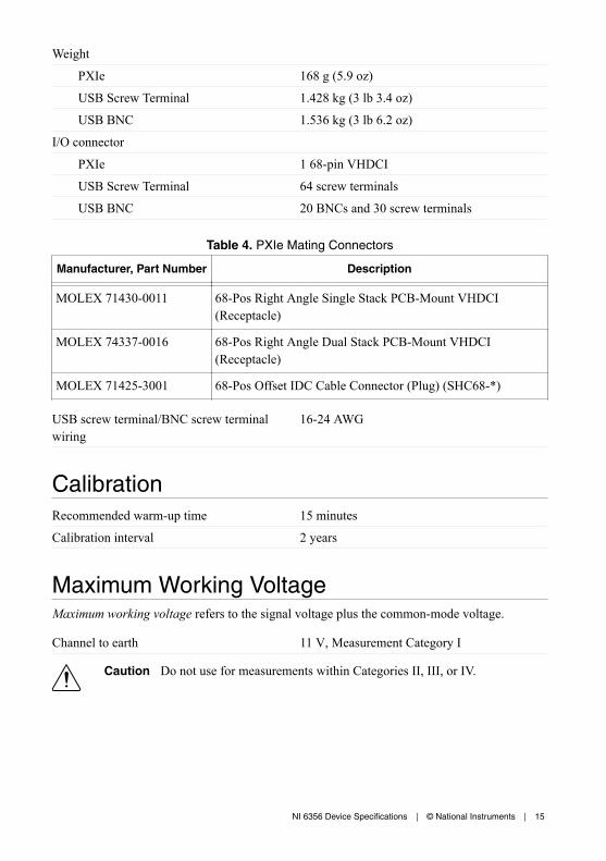
Weight
PXIe 168 g (5.9 oz)
USB Screw Terminal 1.428 kg (3 lb 3.4 oz)
USB BNC 1.536 kg (3 lb 6.2 oz)
I/O connector
PXIe 1 68-pin VHDCI
USB Screw Terminal 64 screw terminals
USB BNC 20 BNCs and 30 screw terminals
Table 4. PXIe Mating Connectors
Manufacturer, Part Number Description
MOLEX 71430-0011 68-Pos Right Angle Single Stack PCB-Mount VHDCI(Receptacle)
MOLEX 74337-0016 68-Pos Right Angle Dual Stack PCB-Mount VHDCI(Receptacle)
MOLEX 71425-3001 68-Pos Offset IDC Cable Connector (Plug) (SHC68-*)
USB screw terminal/BNC screw terminalwiring
16-24 AWG
CalibrationRecommended warm-up time 15 minutes
Calibration interval 2 years
Maximum Working VoltageMaximum working voltage refers to the signal voltage plus the common-mode voltage.
Channel to earth 11 V, Measurement Category I
Caution Do not use for measurements within Categories II, III, or IV.
NI 6356 Device Specifications | © National Instruments | 15
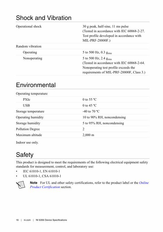
Shock and VibrationOperational shock 30 g peak, half-sine, 11 ms pulse
(Tested in accordance with IEC 60068-2-27.Test profile developed in accordance withMIL-PRF-28800F.)
Random vibration
Operating 5 to 500 Hz, 0.3 grms
Nonoperating 5 to 500 Hz, 2.4 grms(Tested in accordance with IEC 60068-2-64.Nonoperating test profile exceeds therequirements of MIL-PRF-28800F, Class 3.)
EnvironmentalOperating temperature
PXIe 0 to 55 ºC
USB 0 to 45 ºC
Storage temperature -40 to 70 ºC
Operating humidity 10 to 90% RH, noncondensing
Storage humidity 5 to 95% RH, noncondensing
Pollution Degree 2
Maximum altitude 2,000 m
Indoor use only.
SafetyThis product is designed to meet the requirements of the following electrical equipment safetystandards for measurement, control, and laboratory use:• IEC 61010-1, EN 61010-1• UL 61010-1, CSA 61010-1
Note For UL and other safety certifications, refer to the product label or the OnlineProduct Certification section.
16 | ni.com | NI 6356 Device Specifications
Electromagnetic CompatibilityThis product meets the requirements of the following EMC standards for electrical equipmentfor measurement, control, and laboratory use:• EN 61326-1 (IEC 61326-1): Class A emissions; Basic immunity• EN 55011 (CISPR 11): Group 1, Class A emissions• EN 55022 (CISPR 22): Class A emissions• EN 55024 (CISPR 24): Immunity• AS/NZS CISPR 11: Group 1, Class A emissions• AS/NZS CISPR 22: Class A emissions• FCC 47 CFR Part 15B: Class A emissions• ICES-001: Class A emissions
Note In the United States (per FCC 47 CFR), Class A equipment is intended foruse in commercial, light-industrial, and heavy-industrial locations. In Europe,Canada, Australia and New Zealand (per CISPR 11) Class A equipment is intendedfor use only in heavy-industrial locations.
Note Group 1 equipment (per CISPR 11) is any industrial, scientific, or medicalequipment that does not intentionally generate radio frequency energy for thetreatment of material or inspection/analysis purposes.
Note For EMC declarations and certifications, and additional information, refer tothe Online Product Certification section.
CE Compliance This product meets the essential requirements of applicable European Directives, as follows:• 2014/35/EU; Low-Voltage Directive (safety)• 2014/30/EU; Electromagnetic Compatibility Directive (EMC)
Online Product CertificationRefer to the product Declaration of Conformity (DoC) for additional regulatory complianceinformation. To obtain product certifications and the DoC for this product, visit ni.com/certification, search by model number or product line, and click the appropriate link in theCertification column.
NI 6356 Device Specifications | © National Instruments | 17
Environmental ManagementNI is committed to designing and manufacturing products in an environmentally responsiblemanner. NI recognizes that eliminating certain hazardous substances from our products isbeneficial to the environment and to NI customers.
For additional environmental information, refer to the Minimize Our Environmental Impactweb page at ni.com/environment. This page contains the environmental regulations anddirectives with which NI complies, as well as other environmental information not included inthis document.
Waste Electrical and Electronic Equipment (WEEE)EU Customers At the end of the product life cycle, all NI products must bedisposed of according to local laws and regulations. For more information abouthow to recycle NI products in your region, visit ni.com/environment/weee.
电子信息产品污染控制管理办法(中国 RoHS)中国客户 National Instruments 符合中国电子信息产品中限制使用某些有害物
质指令(RoHS)。关于 National Instruments 中国 RoHS 合规性信息,请登录
ni.com/environment/rohs_china。(For information about China RoHScompliance, go to ni.com/environment/rohs_china.)
18 | ni.com | NI 6356 Device Specifications
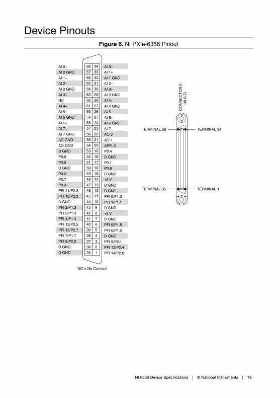
Device PinoutsFigure 6. NI PXIe-6356 Pinout
D GND
D GND
PFI 8/P2.0
PFI 7/P1.7
PFI 15/P2.7
PFI 13/P2.5
PFI 4/P1.4
PFI 3/P1.3
PFI 2/P1.2
D GND
PFI 10/P2.2
PFI 11/P2.3
P0.3
P0.7
P0.2
D GND
P0.5
P0.0
D GND
AO GND
AO GND
AI 7 GND
AI 7+
AI 6–
AI 5 GND
AI 5+
AI 4–
NC
AI 3–
AI 2 GND
AI 2+
AI 1–
AI 0 GND
AI 0+
PFI 14/P2.6
PFI 9/P2.1
D GND
PFI 5/P1.5
D GND
+5 V
D GND
PFI 12/P2.4
PFI 6/P1.6
PFI 1/P1.1
PFI 0/P1.0
D GND
D GND
+5 V
D GND
P0.6
P0.1
D GND
P0.4
APFI 0
AO 1
AO 0
AI 7–
AI 6 GND
AI 6+
AI 5–
AI 4 GND
AI 4+
AI 3 GND
AI 3+
AI 2–
AI 1 GND
AI 1+
AI 0–68 34
67 33
66 32
65 31
64 30
63 29
62 28
61 27
60 26
59 25
58 24
57 23
56 22
55 21
54 20
53 19
52 18
51 17
50 16
49 15
48 14
47 13
46 12
45 11
44 10
43 9
42 8
41 7
40 6
39 5
38 4
37 3
36 2
35 1
TERMINAL 34TERMINAL 68
TERMINAL 1TERMINAL 35
CO
NN
EC
TOR
0(A
I 0-7
)
NC = No Connect
NI 6356 Device Specifications | © National Instruments | 19
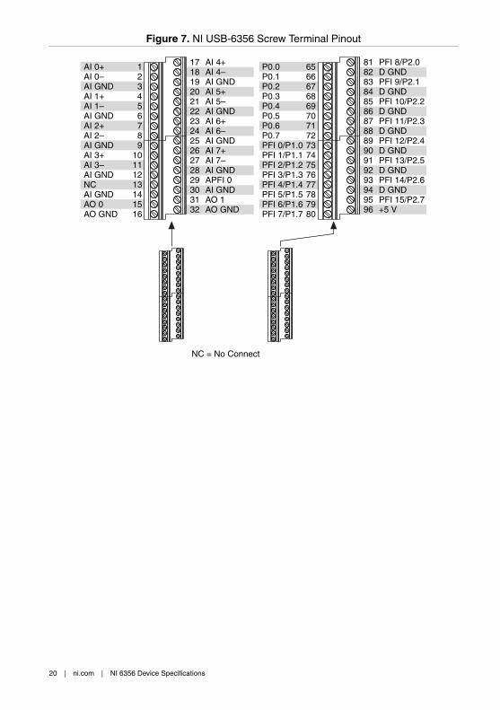
Figure 7. NI USB-6356 Screw Terminal Pinout
17181920212223242526272829303132
AI 4+AI 4–AI GNDAI 5+AI 5–AI GNDAI 6+AI 6–AI GNDAI 7+AI 7–AI GNDAPFI 0AI GNDAO 1AO GND
AI 0+AI 0–AI GNDAI 1+AI 1–AI GNDAI 2+AI 2–AI GNDAI 3+AI 3–AI GNDNCAI GNDAO 0AO GND
123456789
10111213141516
81828384858687888990919293949596
PFI 8/P2.0D GNDPFI 9/P2.1D GNDPFI 10/P2.2D GNDPFI 11/P2.3D GNDPFI 12/P2.4D GNDPFI 13/P2.5D GNDPFI 14/P2.6D GNDPFI 15/P2.7+5 V
P0.0P0.1P0.2P0.3P0.4P0.5P0.6P0.7PFI 0/P1.0PFI 1/P1.1PFI 2/P1.2PFI 3/P1.3PFI 4/P1.4PFI 5/P1.5PFI 6/P1.6PFI 7/P1.7
65666768697071727374757677787980
NC = No Connect
20 | ni.com | NI 6356 Device Specifications
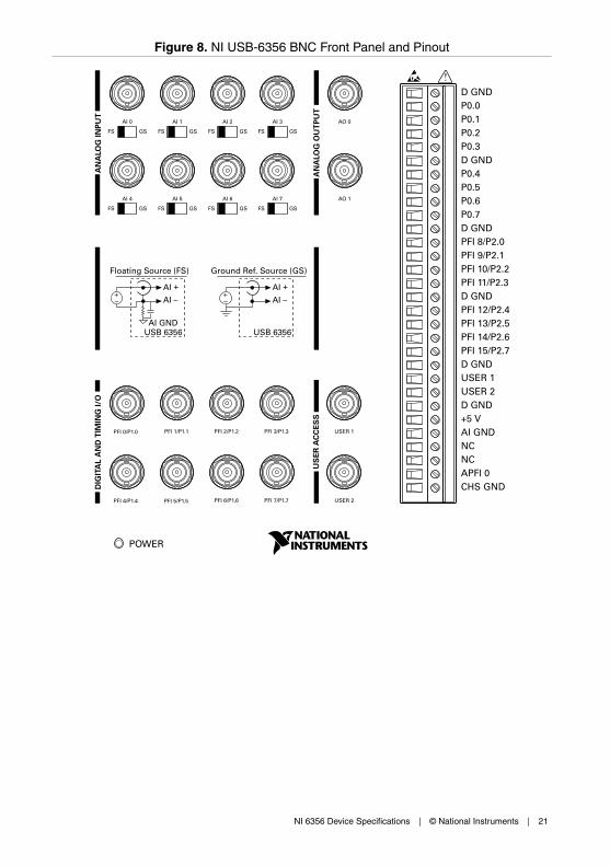
Figure 8. NI USB-6356 BNC Front Panel and Pinout
AN
ALO
G IN
PU
TD
IGIT
AL
AN
D T
IMIN
G I/
O
AN
ALO
G O
UT
PU
T
AI 0
FS GS
AI 1
FS GS
AI 2
FS GS
AI 3
FS GS
AO 0
D GNDP0.0P0.1P0.2P0.3
P0.4P0.5P0.6P0.7
D GND
D GND
D GND
D GND
D GND
AI GNDNCNCAPFI 0CHS GND
+5 V
USER 1USER 2
PFI 8/P2.0PFI 9/P2.1PFI 10/P2.2PFI 11/P2.3
PFI 12/P2.4PFI 13/P2.5PFI 14/P2.6PFI 15/P2.7
PFI 0/P1.0 PFI 1/P1.1 PFI 2/P1.2 PFI 3/P1.3 USER 1
PFI 4/P1.4
POWER
PFI 5/P1.5 PFI 6/P1.6 PFI 7/P1.7 USER 2
AI 4
FS GS
AI 5
FS GS
AI 6
FS GS
AI 7
FS GS
AO 1
US
ER
AC
CE
SS
Floating Source (FS)
AI GND
AI +
AI –+–
USB 6356
Ground Ref. Source (GS)
AI +
AI –+–
USB 6356
NI 6356 Device Specifications | © National Instruments | 21

Refer to the NI Trademarks and Logo Guidelines at ni.com/trademarks for information on NI trademarks. Other product andcompany names mentioned herein are trademarks or trade names of their respective companies. For patents covering NIproducts/technology, refer to the appropriate location: Help»Patents in your software, the patents.txt file on your media, or theNational Instruments Patent Notice at ni.com/patents. You can find information about end-user license agreements (EULAs)and third-party legal notices in the readme file for your NI product. Refer to the Export Compliance Information at ni.com/legal/export-compliance for the NI global trade compliance policy and how to obtain relevant HTS codes, ECCNs, and otherimport/export data. NI MAKES NO EXPRESS OR IMPLIED WARRANTIES AS TO THE ACCURACY OF THE INFORMATIONCONTAINED HEREIN AND SHALL NOT BE LIABLE FOR ANY ERRORS. U.S. Government Customers: The data contained inthis manual was developed at private expense and is subject to the applicable limited rights and restricted data rights as set forthin FAR 52.227-14, DFAR 252.227-7014, and DFAR 252.227-7015.
© 2015—2016 National Instruments. All rights reserved.
374452C-01 Jun16