nie effecrs of leakage inooctance on multi … · nie effecrs of leakage inooctance on multi-()(n...
TRANSCRIPT
nIE EFFEcrs OF LEAKAGE INOOCTANCE ON MULTI-()(n'fI{1r n.YBAa< CIRaJITS
Lloyd H. Dixon, Jr.
A similar topic dealing with buck-derived regulators was presented at previousUnitrode seminars (see Section P2). Leakage inductance is also the majorcause of poor cross-regulation in flyback circuits, but the circuit analysisis quite different. This topic shows how to predict and minimize the effectsof leakage inductance and wiring inductance in continuous and discontinuousmode flyback regulators.
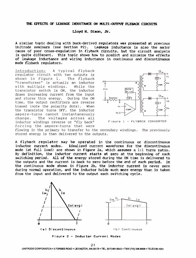
A flyback regulator may be operated in the continuous or discontinuousinductor current modes. Idealized current waveforms for the discontinuousmode (at full load) are shown in Figure 2a, which assumes a 1:1 turns ratio.By definition, the inductor current starts at zero at the beginning of eachswitching period. All of the energy stored during the ON time is delivered tothe outputs and the current is back to zero before the end of each period. Inthe continuous mode shown in Figure 2b, the inductor current is never zeroduring normal operation, and the inductor holds much more energy than is takenfrom the input and delivered to the output each switching cycle.
(a) Discontinuous
F;aure 2- Inductor Current Modes
2-1
UNITRODE CORPORATION. 5 FORBES ROAD. LEXINGTON, MA 02173 .TEL. (617) 861-6540. TWX (710) 326-6509 .TELEX 95-1064
These two inductor current operating modes have radically different operatingcharacteristics, with divergent opinions by experienced designers as to whichmode is better. Note that for the same average output current (same poweroutput), the discontinuous mode reaches nearly twice the peak current requiredin the continuous mode. However, as indicated by the relative inductorcurrent slopes, the continuous mode typically employs 10 times the inductancevalue and requires 10/1.82 = 3 times the inductor energy storage capability asthe discontinuous mode.
Non-Ideal Aspects: All flyback circuits depend upon inductive energy storage.This is usually accomplished by introducing a small non-magnetic gap in serieswith the inductor core. Unfortunately, the inductor windings cannot all beequally well coupled to the energy storage gap because of the physicalseparation between the windings. Additional amounts of magnetic energy arealso stored between and within the windings. These amounts of energy are
represented in the circuit as leakage inductances.
When the transistor turns off, leakage inductance between transformer primaryand secondaries will fight the transfer of current to the secondaries, causinga large voltage spike to occur across the transistor. This inductive spikemust be clamped to a voltage level less than the transistor rating or thetransistor will be destroyed. (Figure 1 does not show this necessary clamp.)There are many possible clamping methods --with some, the energy put into theclamp is lost, hurting circuit efficiency, with other methods the clamp energyis conserved. The two-transistor 150 Watt Flyback Regulator Design Review(Section A3) saves this energy by returning it to the input.
Leakage inductance between secondaries, together with wiring inductances fromeach secondary to its respective filter capacitor, are the main cause of poorcross-regulation between the outputs.
Circuit diagrams such as Figure 1 seldom show these many parasitic inductiveelements which play such an important role in flyback circuit performance.Circuit analysis becomes complex and confusing when all these elements areincluded, compounded by the differing turns ratios between the windings.
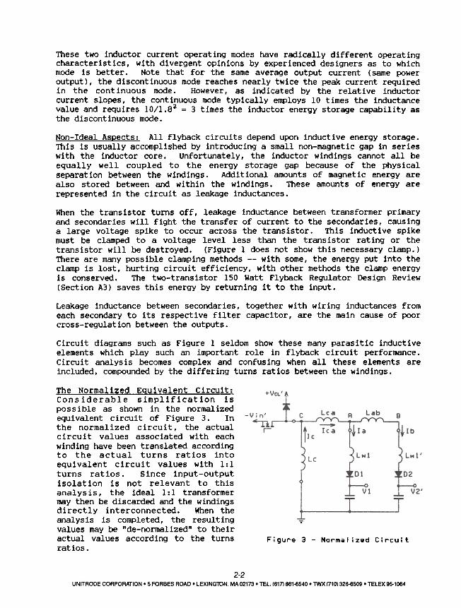
The Normalized Equivalent Circuit:Considerable simplification ispossible as shown in the normalizedequivalent circuit of Figure 3. Inthe normalized circuit, the actualcircuit values associated with eachwinding have been translated accordingto the actual turns ratios intoequivalent circuit values with 1:1
turns ratios. Since input-outputisolation is not relevant to thisanalysis, the ideal 1:1 transformermay then be discarded and the windingsdirectly interconnected. When theanalysis is completed, the resultingvalues may be "de-normalized" to theiractual values according to the turns
ratios.
":"
Figure 3- Norm.1 ized C;~cu;t
2-2
UNITRODE CORPORATION. 5 FORBES ROAD. LEXINGTON. MA 02173 .TEL. (617) 861-6540. TWX(710\ 326-6509 .TELEX 95-1064
For example, assume an off-line regulator with a 30:1 turns ratio betweenprimary and SV secondary, and a 3:1 turns ratio between lSV secondary and theSV secondary. Normalization may be with respect to any winding. In thiscase, all windings are normalized to the 5V winding by dividing each voltageand multiplying current by the actual turns ratio. Inductance and resistanceare divided and capacitance multiplied by the turns ratio squared. Referredto the 5V secondary, a Vin of 300V divided by the turns ratio of 30 translatesto Vin' of 10V. Primary inductance of 450~H divided by 302 becomes 0.5~H.The V2 of 15V at 4A secondary becomes V2' of 5V at 12A, etc.
The normalized circuit of Figure 3, mutual inductance Lc represents energystored in the gap, Lca represents leakage inductance between primary andsecondary A, and Lab is the leakage inductance between secondaries A and B.Mutual inductance Lc is connected directly to Vin' through the transistor orto VCL' through the clamp diode, whereas outputs Vl and V2' are coupled to Lcthrough leakage inductances and secondary wiring inductances Lwl and Lw2.Primary wiring inductance is negligible because it is divided by 302. ThisFigure 3 configuration applies when the primary winding is closest to the gap--either inside the secondaries with the centerleg gapped or outside thesecondaries with the outer leg gapped. If the primary were on the other sideof the secondaries opposite the gap, the equivalent circuit would have Lcconnected to point B instead of point C.
To further simplify the analysis, output ripple voltages are assumed to bezero. The error caused by this assumption is small in a practical powersupplyand its effect nearly averages out over a complete switching period.
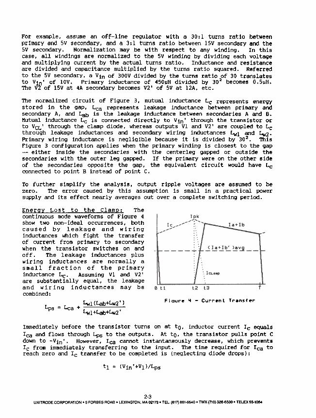
Enerqy Lost to the Clamp: Thecontinuous mode waveforms of Figure 4show two non-ideal occurrences, bothcaused by leakage and wiringinductances which fight the transferof current from primary to secondarywhen the transistor switches on and
off. The leakage inductances pluswiring inductances are normally asmall fraction of the primary
inductance Lc. Assuming VI and V2'are substantially equal, the leakageand wiring inductances may be
combined:F;aur~ ~ -Curr~nt Transt~rLps = Lca + ~l <Lab+Lw2 ' )
Lwl+Lab+Lw2'
Immediately before the transistor turns on at to, inductor current Ic equals
Ica and flows through Lps to the outputs. At to, the transistor pulls point Cdown to -Vin'. However, Ica cannot instantaneously decrease, which preventsIc from immediately transferring to the input. The time required for Ica toreach zero and Ic transfer to be completed is (neglecting diode drops):
tl = (Vin'+Vl>/Lps
2-3UNITRODE CORPORATION. 5 FORBES ROAD. LEXINGTON, MA 02173 .TEL. (617) 661-6540. TWX (710) 326-6509 .TELEX 95-1064
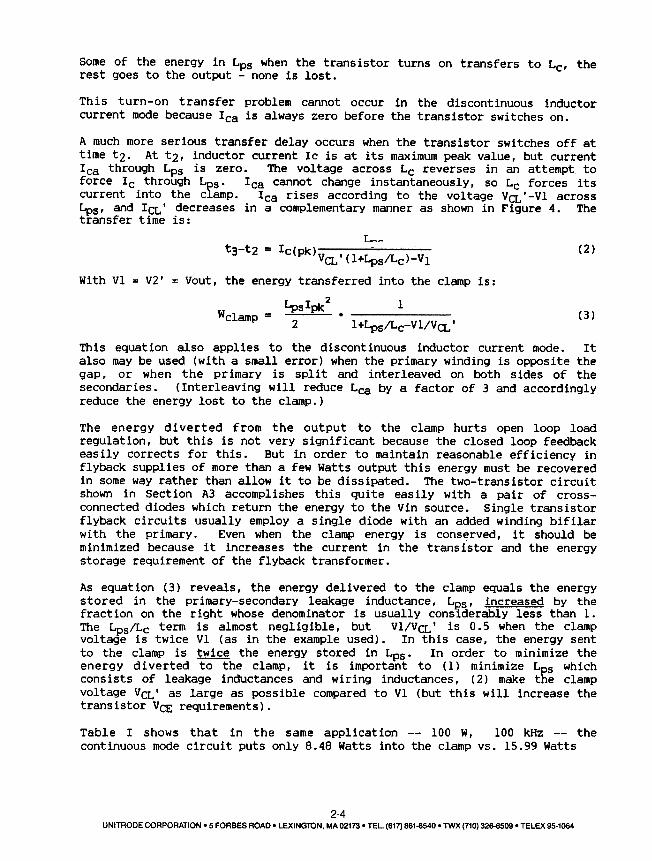
Some of the energy 1n Lps when the transistor turns on transfers to Lc, therest goes to the output -none 1s lost.
This turn-on transfer problem cannot occur in the discontinuous inductorcurrent mode because Ica is always zero before the transistor switches on.
A much more serious transfer delay occurs when the transistor switches off attime t2. At t2, inductor current Ic is at its maximum peak value, but currentIca through Lps is zero. The voltage across Lc reverses in an attempt toforce Ic through Los. Ica cannot change instantaneously, so Lc forces itscurrent into the clamp. Ica rises according to the voltage VCL'-Vl across~S' and ICL' decreases in a complementary manner as shown in Figure 4. Thetransfer time is:
Lp5t3-t2 = Ic(pk) (2)
VCL'(I+Lps/Lc)-VI
With VI = V2' = Vout, the energy transferred into the clamp is:
Lpslpk2 1Wclamp = 2 .I+Lps/Lc-VI/VCL ,
This equation also applies to the discontinuous inductor current mode. Italso may be used (with a small error) when the primary winding is opposite thegap, or when the primary is split and interleaved on both sides of thesecondaries. (Interleaving will reduce Lca by a factor of 3 and accordinglyreduce the energy lost to the clamp.)
(3)
The energy diverted from the output to the clamp hurts open loop loadregulation, but this is not very significant because the closed loop feedbackeasily corrects for this. But in order to maintain reasonable efficiency inflyback supplies of more than a few Watts output this energy must be recoveredin some way rather than allow it to be dissipated. The two-transistor circuitshown in Section A3 accomplishes this quite easily with a pair of cross-connected diodes which return the energy to the Vin source. Single transistorflyback circuits usually employ a single diode with an added winding bifilarwith the primary. Even when the clamp energy is cons~rved, it should beminimized because it increases the current in the transistor and the energystorage requirement of the flyback transformer.
As equation (3) reveals, the energy delivered to the clamp equals the energystored in the primary-secondary leakage inductance, Lps, increased by thefraction on the right whose denominator is usually considerably less than 1.The Lps/Lc term is almost negligible, but VI/VCL' is 0.5 when the clampvoltage is twice VI (as in the example used). In this case, the energy sentto the clamp is ~ the energy stored in Lps. In order to minimize theenergy diverted to the clamp, it is important to (1) minimize L s whichconsists of leakage inductances and wiring inductances, (2) make the clampvoltage VCL' as large as possible compared to VI (but this will increase thetransistor VCE requirements).
Table I shows that in the same application --100 W, 100 kHz --thecontinuous mode circuit puts only 8.48 Watts into the clamp vs. 15.99 Watts
2-4
UNITRODE CORPORATION. 5 FORBES ROAD. LEXING1ON, MA 02173 .TEL. (617) 661-6540. TWX (710) 326-6509 .TELEX 95-1064
for the continuous mode. Even though Ipk in the discontinuous mode is almosttwice as large, primary-secondary inductance Lps is 6 times smaller whichgives the advantage to the discontinuous mode. The ~s would be even smallerfovoring the discontinuous mode even more but the wiring inductance which isthe same in both circuits is a much more significant portion of thediscontinuous mode Lps.
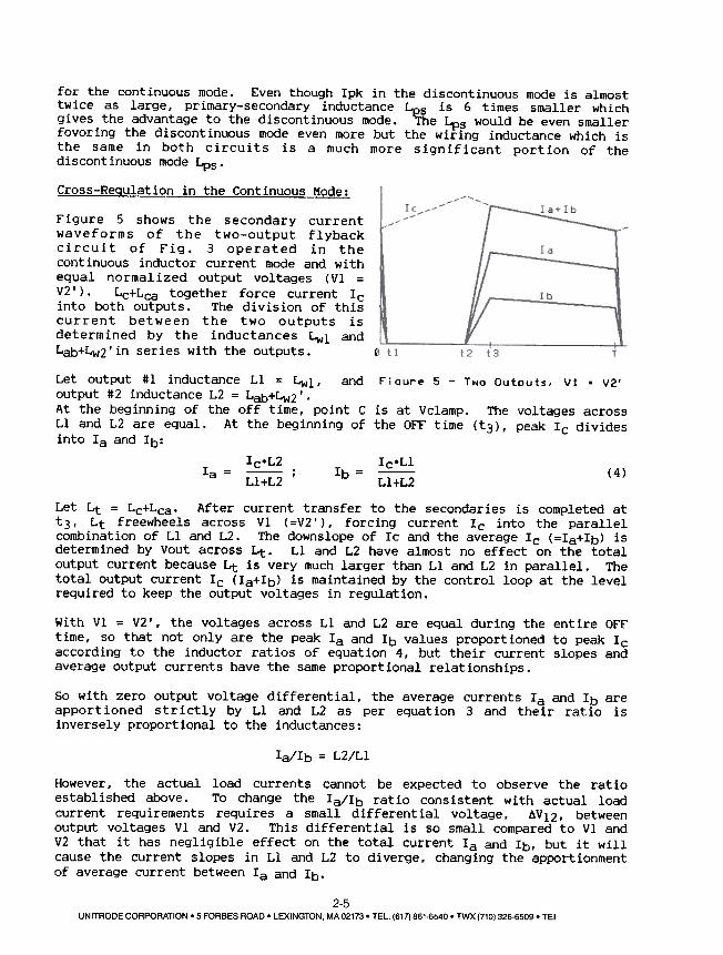
Cross-Regulation in the Continuous Mode:
Ia+IbFigure 5 shows the secondary currentwaveforms of the two-output flybackcircuit of Fig. 3 operated in thecontinuous inductor current mode and withequal normalized output voltages (VI =
V2'). Lc+Lca together force current Icinto both outputs. The division of thiscurrent between the two outputs isdetermined by the inductances LwI and
Lab+Lw2'in series with the outputs. 0 tt t2 t3
Let output #1 inductance Ll = Lwl, and Fiour~ 5- Two Outputs, Vl = V2'
output #2 inductance L2 = Lab+Lw2'.
At the beginning of the off time, point C is at V clamp. The voltages acrossLl and L2 are equal. At the beginning of the OFF time (t3), peak lc divides
into la and lb:
Ic.L2-0
,Ll+L2
Ic.Ll
Ll+L2Ib = (4)la =
Let Lt = Lc+Lca. After current transfer to the secondaries is completed att3, Lt freewheels across VI <=V2'), forcing current Ic into the parallelcombination of LI and L2. The downs lope of Ic and the average Ic <=Ia+lb) isdetermined by Vout across Lt. LI and L2 have almost no effect on the totaloutput current because Lt is very much larger than LI and L2 in parallel. Thetotal output current Ic <Ia+lb) is maintained by the control loop at the levelrequired to keep the output voltages in regulation.
With VI = V2', the voltages across LI and L2 are equal during the entire OFFtime, so that not only are the peak la and lb values proportioned to peak lcaccording to the inductor ratios of equation 4, but their current slopes andaverage output currents have the same proportional relationships.
So with zero output voltage differential, the average currents la and Ib areapportioned strictly by Ll and L2 as per equation 3 and their ratio isinversely proportional to the inductances:
Ia/lb = L2/Ll
However, the actual load currents cannot be expected to observe the ratioestablished above. To change the la/lb ratio consistent with actual load
current requirements requires a small differential voltage, ~VI2, betweenoutput voltages VI and V2. This differential is so small compared to VI andV2 that it has negligible effect on the total current la and lb, but it willcause the current slopes in LI and L2 to diverge, changing the apportionment
of average current between la and lb.
2-5
UNITRODE CORPORATION. 5 FORBES ROAD. LEXINGTON, MA 02173 .TEL. (617) 861-6540. TWX (710) 326-6509. TEl
!.a-:~b=IcVl=V2'
AV2=2~
}~.~
~ ~ .-:-; .-:-:
--
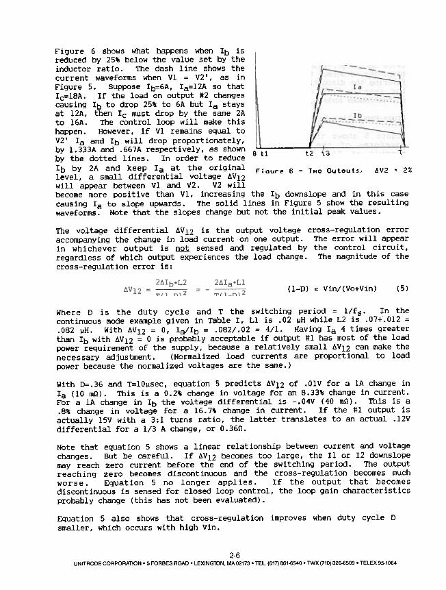
Figure 6 shows what happens when Ib isreduced by 25' below the value set by theinductor ratio. The dash line shows thecurrent waveforms when V1 = V2', as inFigure 5. Suppose Ib=6A, Ia=12A so thatIc=1BA. If the load on output #2 changescausing Ib to drop 25' to 6A but la staysat 12A, then Ic must drop by the same 2Ato 16A. The control loop will make thishappen. However, if V1 remains equal toV2' la and Ib will drop proportionately, IIby 1.333A and .667A respectively, as shown 91 ' ~3by the dotted lines. In order to reduce t t2
Ib by 2A and keep la at the original F . 6 T O t t ' V2 2 .'..lour~ -NO u au s, ..= ,.
level, a small dlfferentlal voltage AV12will appear between V1 and V2. V2 willbecome more positive than V1, increasing the Ib downslope and in this casecausing la to slope upwards. The solid lines in Figure 5 show the resultingwaveforms. Note that the slopes change but not the initial peak values.
The voltage differential 6V12 is the output voltage cross-regulation erroraccompanying the change in load current on one output. The error will appearin whichever output is D.Qt sensed and regulated by the control circuit,regardless of which output experiences the load change. The magnitude of thecross-regulation error is:
(I-D) = Vin/(Vo+Vin) (5)
Where D is the duty cycle and T the switching period = l/fs. In thecontinuous mode example given in Table I, L1 is .02 uH while L2 is .07+.012 =.082 uH. With ~V12 = 0, Ia/lb = .082/.02 = 4/1. Having la 4 times greaterthan Ib with ~V12 = 0 is probably acceptable if output #1 has most of the loadpower requirement of the supply, because a relatively small ~V12 can make thenecessary adjustment. (Normalized load currents are proportional to loadpower because the normalized voltages are the same.)
With 0=.36 and T=10~sec, equation 5 predicts ~V12 of .01V for a 1A change inla (10 ron). This is a 0.2% change in voltage for an 8.33% change in current.For a 1A change in Ib the voltage differential is -.04V (40 ron). This is a.8' change in voltage for a 16.7' change in current. If the #1 output isactually 15V with a 3:1 turns ratio, the latter translates to an actual .12Vdifferential for a 1/3 A change, or O.36n.
Note that equation 5 shows a linear relationship between current and voltagechanges. But be careful. If ~V12 becomes too large, the II or 12 downs lopemay reach zero current before the end of the switching period. The outputreaching zero becomes discontinuous and the cross-regulation becomes muchworse. Equation 5 no longer applies. If the output that becomesdiscontinuous is sensed for closed loop control, the loop gain characteristicsprobably change (this has not been evaluated).
Equation 5 also shows that cross-regulation improves when duty cycle D
smaller, which occurs with high Vin.
2-6UNITRODE CORPORATION. 5 FORBES ROAD. LEXINGTON, MA 02173 .TEL. (617) 861-6540. TWX(710) 326-6509 .TELEX 95-1064
~
la
-
~,
r/
la+Ib=Ic
IIt;
/
/, f
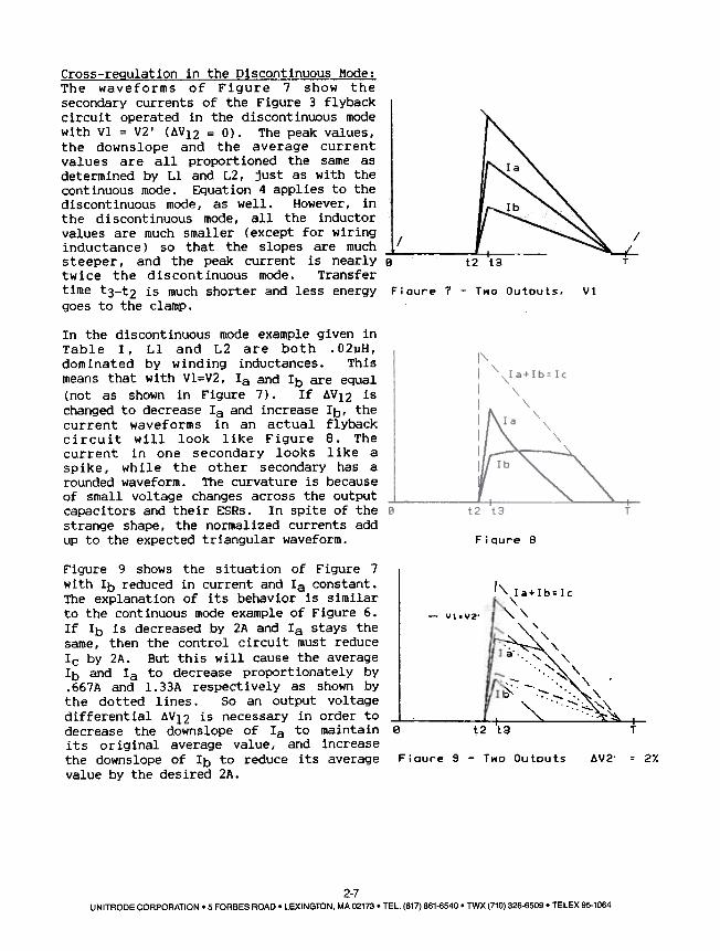
Cross-reQulation in the Discontinuous Mode:The waveforms of Figure 7 show thesecondary currents of the Figure 3 flybackcircuit operated in the discontinuous modewith VI = V2' (6VI2 = 0). The peak values,the downs lope and the average currentvalues are all proportioned the same asdetermined by LI and L2, just as with thecontinuous mode. Equation 4 applies to thediscontinuous mode, as well. However, inthe discontinuous mode, all the inductorvalues are much smaller (except for wiringinductance) so that the slopes are muchsteeper, and the peak current is nearly 0 t2 t3twice the discontinuous mode. Transfertime t3-t2 is much shorter and less energy Fiaure ? -T~o OutDuts,goes to the clamp.
Vi
In the discontinuous mode example given inTable I, Ll and L2 are both .02~H,dominated by winding inductances. Thismeans that with Vl=V2, la and Ib are equal(not as shown in Figure 7). If AV12 ischanged to decrease la and increase Ib, thecurrent waveforms in an actual flybackcircuit will look like Figure 8. Thecurrent in one secondary looks like aspike, while the other secondary has arounded waveform. The curvature is becauseof small voltage changes across the outputcapacitors and their ESRs. In spite of the 0strange shape, the normalized currents addup to the expected triangular waveform.
I'
,Ia+Ib= Ic
,
la
t2 t3
Fioure 8
Figure 9 shows the situation of Figure 7with lb reduced in current and la constant.The explanation of its behavior is similarto the continuous mode example of Figure 6.If lb is decreased by 2A and la stays thesame, then the control circuit must reducelc by 2A. But this will cause the averagelb and la to decrease proportionately by.667A and 1.33A respectively as shown bythe dotted lines. So an output voltagedifferential ~V12 is necessary in order todecrease the downslope of la to maintain eits original average value, and increasethe downs lope of lb to reduce its averagevalue by the desired 2A.
1,\. Ia~Ib=Ic" '\.
""\.-Vl.V2'
-AV2'2~
t2 t3 T
, r-:.. :-:I~. -
AV2' = 2%Fiaure 9- Two Outouts
2-7UNITRODE CORPORATION. 5 FORBES ROAD. LEXINGTON. MA 02173 .TEL. {617) 861-6540. TWX (710) 326-6509. TELEX 95-1064
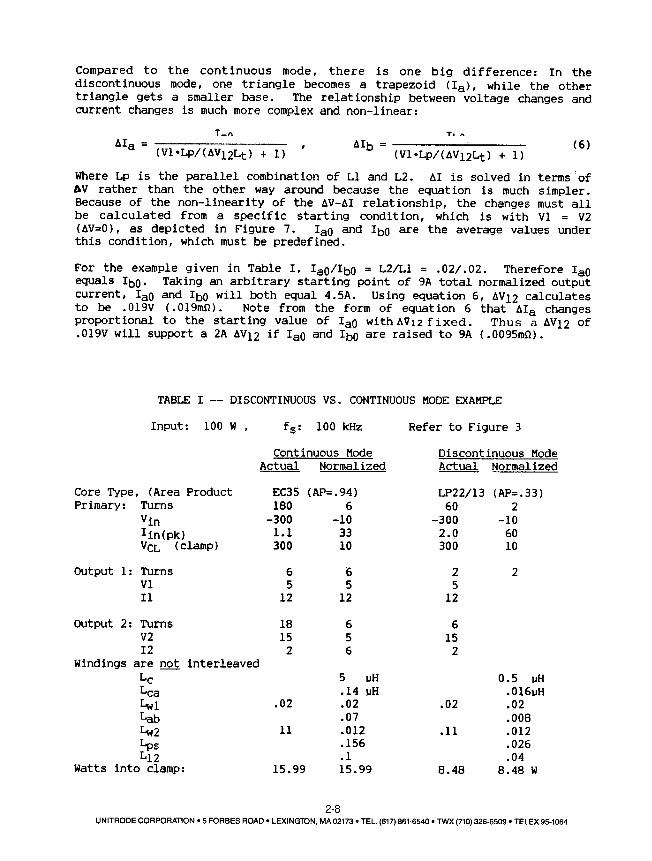
Compared to the continuous mode, there is one big difference: In thediscontinuous mode, one triangle becomes a trapezoid CIa), while the othertriangle gets a smaller base. The relationship between voltage changes andcurrent changes is much more complex and non-linear:
IaO IbOAla = --(Vl.LP/(AV12Lt) + 1) (Vl.Lp/(AVI2Lt) + 1)
Where Lp is the parallel combination of Ll and L2. A1 is solved in terms ofAV rather than the other way around because the equation is much simpler.Because of the non-linearity of the AV-Al relationship, the changes must allbe calculated from a specific starting condition, which is with VI = V2(AV=O), as depicted in Figure 7. laO and IbO are the average values underthis condition, which must be predefined.
dlh = (6)
For the example given in Table I, IaO/IbO = L2/L1 = .02/.02. Therefore IaOequals IbO. Taking an arbitrary starting point of 9A total normalized outputcurrent, IaO and IbO will both equal 4.5A. Using equation 6, ~V12 calculatesto be .019V (.019mQ). Note from the form of equation 6 that ~Ia changesproportional to the starting value of IaO with AV12 f ixed .Thus a ~V12 of.019V will support a 2A ~V12 if IaO and IbO are raised to 9A (.0095mQ).
TABLE I --DISCONTINUOUS VS. CONTINUOUS MODE EXAMPLE
Input: 100 W , fs: 100 kHz Refer to Figure 3
Continuous ModeActual Normalized
Discontinuous ModeActual Normalized
E:C35 (AP=.94)
180 6
-300 -101.1 33300 10
LP22/13 (AP=.33)60 2
-300 -102.0 60300 10
Core Type, (Area ProductPrimary: Turns
VinIin(pk)VCL (clamp)
Output 1: TurnsVIII
25
12
265
12
65
12
1815
2
656
615
2
output 2: TurnsV212
Windings are DQi interleaved
LcLcaLwlLabLw2LpsL12
Watts into clamp:
5 }!H
.14 }!H
.02
.07
.012
.156
.1
15.99
0.5 uH.016uH.02.008.012.026.04
8.48 W
.02 .02
11 .11
15.99 8.48
2-8
UNITRODE CORPORATION. 5 FORBES ROAD. LEXINGTON, MA 02173 .TEL. (617) 881-6540. TWX (710) 326-6509. TELEX 95-1064

How to Calculate the Amount of Leakage Inductance: Leakage inductancerepresents the energy storage between two windings. It may be roughlycalculated from the winding geometry, using the inductance formula:
L = N2~o~r.Area/Length x 10-2
In the S.I. system of units, Uo = 4uol0-7. For the non-magnetic materialsbetween and within the windings, ur = 1. For concentric coils, "Area" is thecross-section in cm2 of the hollow cylindrical shape between the windings {thedistance from the middle of one winding to the middle of the other, multipliedby the average length of one turn). "Length" is the length of the cylindricalshape --the length of the winding in cm2, or the breadth of the windingwindow. N is the number of turns in the whichever winding the leakageinductance will be referenced to. With the windings normalized, it doesn'tmake any difference.
How to Minimize Leakage Inductance:
1. Windings must be long and thin (few layers) for intimate coupling. Potcores have very poor window form factor -windings are short and thick.Ferrite ETD and LP cores are good. Mo-Permalloy powder toriods provide thebest winding form factor but they are probably too lossy for use indiscontinuous mode applications because of the large flux swings involved.
2. Secondaries ~ be tightly coupled to get good cross-regulation. Windmultifilar, otherwise as close together as possible. Don't sandwich theprimary between two secondaries. This reduces eddy current losses but hurtscross-regulation.
3. Primary to secondary leakage inductance does not hurt cross-regulation,but it does divert much of the inductor energy into the clamp. In off-lineapplications, insulation requirements force significant area between primaryand secondary windings which cam make the leakage inductance quite large. Ifnecessary, interleave the primary and secondaries by putting on half theprimary turns, then all the secondaries, then the other half of the primaryturns outside the secondaries. The primary halves must be series connected.(Never parallel windings that are at different levels in the winding structureor large circulating current will result.) Interleaving will reduce primary-secondary leakage inductance by a factor of ~, but it reduces the leakageinductance between secondaries very little and therefore has little effect oncross-regulation.
How to Minimize Wirinq Inductance:
in low voltage, high current outputs.
Wiring inductance is especially critical
1. Minimize the area enclosed by the loop from the transformer secondarythrough the rectifier to the filter capacitor and back to the secondary. Keepthe distances as short as possible and keep the outward and return conductorsvery close to each other. A ground plane is no good for the return pathunless the outward conductor is held very close to it.
2-9
UNITRODE CORPORATION. 5 FORBES ROAD. LEXINGTON, MA 02173 .TEL. (617) 861-6540. TWX (710) 326-6509. TELEX 95-1064

2. Don't use round wire, use flat strip or braid with their breadths facingeach other as closely as possible. Two copper strips 1 cm wide and 10 cm longspaced 0.3 cm apart have a total inductance of 20 nH. Spread apart, theinductance will rise to loo nH.
What Sequence for the Secondaries: Referring to Figure 3, with zerodifferential between the normalized output voltages, the output currents willdivide according to the ratio of inductances Lwl vs. Lab+Lw2'. A high voltage
output will usually have much lower normalized wiring inductance (because it
is reduced by N2). If the high voltage output is in position 1 with theclosest coupling to the primary, it will take most of the normalized current(and power output). A large differential offset will be required to forcepower to output .2 to achieve a better balance.
Because the low voltage output has higher normalized wiring inductance, itusually makes sense to put it in the #1 position closest to the primary, whereits wiring inductance helps to balance out leakage inductance Lab. This willprovide better distribution of power without requiring as much output voltageoffset. Better balance can be achieved by deliberately increasing wiringinductance selectively, but this will hurt cross-regulation.
9/86
2-10
UNITRODE CORPORATION. 5 FORBES ROAD. LEXINGmN, MA 02173 .TEL. (617) 861-6540. TWX (710) 326-6509. TELEX 95-1064

IMPORTANT NOTICE
Texas Instruments and its subsidiaries (TI) reserve the right to make changes to their products or to discontinueany product or service without notice, and advise customers to obtain the latest version of relevant informationto verify, before placing orders, that information being relied on is current and complete. All products are soldsubject to the terms and conditions of sale supplied at the time of order acknowledgment, including thosepertaining to warranty, patent infringement, and limitation of liability.
TI warrants performance of its products to the specifications applicable at the time of sale in accordance withTI’s standard warranty. Testing and other quality control techniques are utilized to the extent TI deems necessaryto support this warranty. Specific testing of all parameters of each device is not necessarily performed, exceptthose mandated by government requirements.
Customers are responsible for their applications using TI components.
In order to minimize risks associated with the customer’s applications, adequate design and operatingsafeguards must be provided by the customer to minimize inherent or procedural hazards.
TI assumes no liability for applications assistance or customer product design. TI does not warrant or representthat any license, either express or implied, is granted under any patent right, copyright, mask work right, or otherintellectual property right of TI covering or relating to any combination, machine, or process in which suchproducts or services might be or are used. TI’s publication of information regarding any third party’s productsor services does not constitute TI’s approval, license, warranty or endorsement thereof.
Reproduction of information in TI data books or data sheets is permissible only if reproduction is withoutalteration and is accompanied by all associated warranties, conditions, limitations and notices. Representationor reproduction of this information with alteration voids all warranties provided for an associated TI product orservice, is an unfair and deceptive business practice, and TI is not responsible nor liable for any such use.
Resale of TI’s products or services with statements different from or beyond the parameters stated by TI forthat product or service voids all express and any implied warranties for the associated TI product or service,is an unfair and deceptive business practice, and TI is not responsible nor liable for any such use.
Also see: Standard Terms and Conditions of Sale for Semiconductor Products. www.ti.com/sc/docs/stdterms.htm
Mailing Address:
Texas InstrumentsPost Office Box 655303Dallas, Texas 75265
Copyright 2001, Texas Instruments Incorporated