nlm0011/ nlm0010 nfc-pwm series - infineon technologies
TRANSCRIPT

NLM0011/ NLM0010 " NFC-PWM Series "NFC Wireless Configuration IC with PWM Output
Features• Configurable pulse width modulation (PWM) output• NFC contactless interface compliant to ISO/IEC 18000-3 mode 1 (ISO/IEC 15963)• Constant light output (CLO) with 8 configurable reference points• Integrated operation-time counter (OTC) and on/off counter• Non-volatile memory (NVM) including UID and 20 bytes free memory for user data
DescriptionThe NLM0011 is a dual-mode NFC wireless configuration IC with PWM output. It is compatible with existinganalog LED-driver designs and with the NFC-programming specification from the Module-Driver InterfaceSpecial Interest Group (MD-SIG). This device is primarily designed for LED applications to enable NFCprogramming. In addition, advanced features such as the constant lumen output (CLO) as well as the on/offcounting are integrated, and there is no need for an additional microcontroller. Since the NLM0011 is designedto work together with mainstream analog driver ICs, there are no firmware development efforts needed. It canbe easily adapted into existing designs to replace the “plug-in resistor” current configuration concept. TheNLM0010 is a light version without CLO function.
Datasheet Please read the Important Notice and Warnings at the end of this document 2.0www.infineon.com 2019-05-31

Table of contents
Features . . . . . . . . . . . . . . . . . . . . . . . . . . . . . . . . . . . . . . . . . . . . . . . . . . . . . . . . . . . . . . . . . . . . . . . . . . . . . . . 1
Description . . . . . . . . . . . . . . . . . . . . . . . . . . . . . . . . . . . . . . . . . . . . . . . . . . . . . . . . . . . . . . . . . . . . . . . . . . . . .1
Table of contents . . . . . . . . . . . . . . . . . . . . . . . . . . . . . . . . . . . . . . . . . . . . . . . . . . . . . . . . . . . . . . . . . . . . . . . 2
1 General . . . . . . . . . . . . . . . . . . . . . . . . . . . . . . . . . . . . . . . . . . . . . . . . . . . . . . . . . . . . . . . . . . . . . . . . . . . . . . . . 3
2 Feature Overview . . . . . . . . . . . . . . . . . . . . . . . . . . . . . . . . . . . . . . . . . . . . . . . . . . . . . . . . . . . . . . . . . . . . . . .4
3 Application Overview . . . . . . . . . . . . . . . . . . . . . . . . . . . . . . . . . . . . . . . . . . . . . . . . . . . . . . . . . . . . . . . . . . . 6
4 Pin Description . . . . . . . . . . . . . . . . . . . . . . . . . . . . . . . . . . . . . . . . . . . . . . . . . . . . . . . . . . . . . . . . . . . . . . . . . 8
5 Functional Description . . . . . . . . . . . . . . . . . . . . . . . . . . . . . . . . . . . . . . . . . . . . . . . . . . . . . . . . . . . . . . . . . .9
6 Memory Organization . . . . . . . . . . . . . . . . . . . . . . . . . . . . . . . . . . . . . . . . . . . . . . . . . . . . . . . . . . . . . . . . . .11
7 Application and User Memory Access Control . . . . . . . . . . . . . . . . . . . . . . . . . . . . . . . . . . . . . . . . . . . 17
8 NLM0011/NLM0010 EEPROM Shipment Content (Infineon to Customer) . . . . . . . . . . . . . . . . . .21
9 Constant Lumen Output (CLO) and Operating Time Counting (OTC) . . . . . . . . . . . . . . . . . . . . . . 23
10 PWM Overview . . . . . . . . . . . . . . . . . . . . . . . . . . . . . . . . . . . . . . . . . . . . . . . . . . . . . . . . . . . . . . . . . . . . . . . . 26
11 NLM0011/ NLM0010 Command Set . . . . . . . . . . . . . . . . . . . . . . . . . . . . . . . . . . . . . . . . . . . . . . . . . . . . . 27
12 NLM0011/ NLM0010 Electrical Characteristics . . . . . . . . . . . . . . . . . . . . . . . . . . . . . . . . . . . . . . . . . . . 31
13 Package Outline . . . . . . . . . . . . . . . . . . . . . . . . . . . . . . . . . . . . . . . . . . . . . . . . . . . . . . . . . . . . . . . . . . . . . . . 34
Revision history . . . . . . . . . . . . . . . . . . . . . . . . . . . . . . . . . . . . . . . . . . . . . . . . . . . . . . . . . . . . . . . . . . . . . . . 34
Disclaimer . . . . . . . . . . . . . . . . . . . . . . . . . . . . . . . . . . . . . . . . . . . . . . . . . . . . . . . . . . . . . . . . . . . . . . . . . . . . 35
NLM0011/ NLM0010 " NFC-PWM Series "NFC Wireless Configuration IC with PWM Output
Table of contents
Datasheet 2 2.02019-05-31

1 GeneralGeneral information of NLM0011/ NLM0010 are given here.The NLM0011/NLM0010 belongs to the "NFC-PWM Series" product family and is used in LED lightingapplications together with a current adjustable LED driver.The NLM0011/NLM0010 operates in two operating modes:• Configuration Mode - exclusively used to configure the device via NFC
The NLM0011/NLM0010 enables a LED lighting module manufacturer to configure the LED lighting controlof the module according to the characteristics of connected LED light. This configuration step completesthe LED module manufacturing process and can be done contactless without powering the LED module.The final configuration of the LED module is done via Near Field Communication (NFC) between theconfiguration station and the LED module. The NLM0011/NLM0010 chip provides the NFC transceiverfunctions of the LED module and includes a non volatile memory (NVM) for storing the configuration data.The configuration data usually consist of the LED driver current setpoint value and a life time adjustment .The life time adjustment function compensates the aging effect of the LEDs by adjusting the LED setpointcurrent value according to the accumulated operating hours of the LEDs (NLM0011 only). Therefore theNLM0011 counts the operating hours of the connected LED and adjusts the LED current set point value to aaging function, which is configured via near field communication during the configuration step. Inconfiguration mode, the content of the NVM can be read out via NFC by an external NFC reader. Inconfiguration mode the NLM0011/NLM0010 is powered by the harvested energy of the NFC field. The deviceonly enters the configuration mode, if the external supply voltage VCC is switched off, before applying theNFC field. After completion of NFC configuration the NFC field has to be removed before applying a supplyon pin VCC in order to release the configuration as valid. The configuration mode is left by removing the NFCreader field. During NFC configuration mode the PWM output is inactive and switched to High Impedance("High-Z").
• Lighting Operational Mode - exclusively used to provide a stored configuration in lighting applicationIn lighting Operational Mode the NLM0011/NLM0010 is powered from the external Vcc source of the lightingmodule. The NLM0011/NLM0010 enters the lighting operational mode, if an external VCC source is presentand the device is not in configuration mode. After powering up, means applying external VCC and no NFCfield is present, when applying external VCC, the NLM0011/NLM0010 reads the LED current setpoint valueconfiguration from the integrated NVM and configures a pulse width modulation (PWM) unit. The PWMcycle period and duty cycle contain the information of the LED current setpoint value. The PWM data areoutput of the chip and will be converted into an analog value externally or directly delivered to the LEDcontroller (depending on the used external LED controller). The operation hours are counted and the LEDcurrent setpoint value is adjusted according to the aging function by changing the PWM output accordingly(NLM0011 only). That also implies that the NLM0011/NLM0010 accumulates the overall operating hours ofthe LEDs . That also requires to count the power on times, to store the current value of operating hoursperiodically into the NVM and to detect a power off event of the lighting system, in order to store thecurrent value of operating hours at the moment of power off. In lighting operational mode the NLM0011/NLM0010 does not communicate and does not respond to external NFC link partners and hence no externalNVM access is possible. That means applying an NFC field to the device which already entered the lightingoperational does not have any effect.
NLM0011/ NLM0010 " NFC-PWM Series "NFC Wireless Configuration IC with PWM Output
1 General
Datasheet 3 2.02019-05-31

2 Feature OverviewNLM0011/NLM0010 product features are given here.Product FeaturesContactless Interface• Physical interface and Anti collision compliant to ISO/ IEC 18000-3 mode 1 (ISO/IEC 15693)
- contactless transmission of data and supply energy- data rate up to 26.69 kbit/s- operation frequency: 13.56 MHz- Anti-collision method complying with ISO/IEC 18000-3 mode 1 with identification rate of up to 50 tags/s
• AFI according ISO/IEC 18000-3 mode 1• Read / write distance up to 150 cm (influenced by external circuitry i.e. reader and antenna design)Command Set• Support of error codes 01H, 0FH, 10H, 12H according to ISO/ IEC 18000-3 mode 1• If a command is sent to the NLM0011/NLM0010 which has an invalid frame length no response is returned• Following command set is supported:
- Inventory (command code 01H)- StayQuiet (command code 02H)- ReadSingleBlock (command code 20H)- WriteSingleBlock (command code 21H)- Select (command code 25H)- ResetToReady (command code 26H)- WriteAFI (command code 27H)- LockAFI (command code 28H)- WriteByte (custom command - ISO command code A0H; custom embedded command code 90H)
Non Volatile Memory (NVM)An Infineon EEPROM is used.• size 576 Bit• User area 52 bytes, organized in 13 free user blocks• Each block organized in 4 bytes• Service area 12 bytes• Unique chip identification number• Each block can be permanently locked against overwriting• EEPROM programming time per page < 4 ms• EEPROM endurance minimum 100,000 erase/write cycles• Data retention minimum 10 yearsSupply Conceptoperation mode dependent:• in Lighting Operation mode the chip is supplied by external voltage source
- external supply voltage in the range of 3 … 5V- internal voltage regulator (LDO) is generating a stabilized internal supply- if external supply voltage is present, then the device cannot be supplied by harvesting energy from the
NFC field
NLM0011/ NLM0010 " NFC-PWM Series "NFC Wireless Configuration IC with PWM Output
2 Feature Overview
Datasheet 4 2.02019-05-31

- if external supply voltage is present, NVM cannot accessed by external reader- the device is detecting switch off of external power supply by observing the external supply voltage
level and detecting the resulting under voltage condition. The system has stored energy - internal andexternal capacitance - to save the current system status into the NVM before the power disappears.
• in configuration mode the device is supplied from the harvested energy of the electromagnetic field of theNFC reader.
LED Current Setpoint Definition by PWM• typical logical levels of PWM output are 0V (logic Low) and 2.8V (logic High)• period/ Frequency of PWM signal programmable between 1kHz and 30kHz• Duty cycle programmable between 0% and 100%• resolution/ granularity depends on PWM Frequency (~14.73 bit@ 1kHz; ~9.82bit@30kHz)Operational Time Counting (OTC)The Device is counting the operation hours and stores the value of overall operation time every 4 hours into theNVM. The device detects a power-off event and stores the current value of operation into the NVM before thechip is switched off.On/ Off CountingThe device is counting the number of power on/ power off cycles and stores it in NVM.Constant Lumen Output (CLO) (NLM0011 only)The device is able to adjust the LED current setpoint value depending on an aging function over operating time.The aging function is end customer defined and stored in the NVM within device configuration. The agingfunction is defined between reference points. The setpoint value is interpolated between the setpoints, bytaking the actual accumulated operating time into account. This feature is not available in NLM0010.
NLM0011/ NLM0010 " NFC-PWM Series "NFC Wireless Configuration IC with PWM Output
2 Feature Overview
Datasheet 5 2.02019-05-31
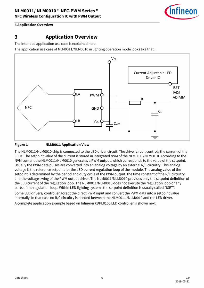
3 Application OverviewThe intended application use case is explained here.The application use case of NLM0011/NLM0010 in lighting operation mode looks like that :
Current Adjustable LED Driver IC
ISETIADJADIMM
LA
LB
GND
PWM
VCC
R1
C1
CVCC
VCC
NFC
Figure 1 NLM0011 Application View
The NLM0011/NLM0010 chip is connected to the LED driver circuit. The driver circuit controls the current of theLEDs. The setpoint value of the current is stored in integrated NVM of the NLM0011/NLM0010. According to theNVM content the NLM0011/NLM0010 generates a PWM output, which corresponds to the value of the setpoint.Usually the PWM data pulses are converted into an analog voltage by an external R/C circuitry. This analogvoltage is the reference setpoint for the LED current regulation loop of the module. The analog value of thesetpoint is determined by the period and duty cycle of the PWM output, the time constant of the R/C circuitryand the voltage swing of the PWM output driver. The NLM0011/NLM0010 provides only the setpoint definition ofthe LED current of the regulation loop. The NLM0011/NLM0010 does not execute the regulation loop or anyparts of the regulation loop. Within LED lighting systems the setpoint definition is usually called "ISET".Some LED drivers/ controller accept the direct PWM input and convert the PWM data into a setpoint valueinternally. In that case no R/C circuitry is needed between the NLM0011 /NLM0010 and the LED driver.A complete application example based on Infineon XDPL8105 LED controller is shown next:
NLM0011/ NLM0010 " NFC-PWM Series "NFC Wireless Configuration IC with PWM Output
3 Application Overview
Datasheet 6 2.02019-05-31
Input
Optional VCC
regulator
NP
Lp
Lp,lk
NS
NA
Vout,diode,drop
CEMI
RCS
RZCD,1
RHV
VCC
CS
GD
GND
RZCD,2
ZCD
CVCC
XDPL8105
Output
HV
Iout
Antenna LALB
PWM
VCC
NLM0011
GND
Ground
VCC power supply
Set the rated LED currentC2
C1
DIM
R
Dual Mode NFC Configuration
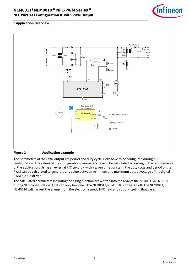
Figure 2 Application example
The parameters of the PWM output are period and duty cycle. Both have to be configured during NFCconfiguration. The values of the configuration parameters have to be calculated according to the requirementsof the application. Using an external R/C circuitry with a given time constant, the duty cycle and period of thePWM can be calculated to generate any value between minimum and maximum output voltage of the digitalPWM output driver.The calculated parameters including the aging function are written into the NVM of the NLM0011/NLM0010during NFC configuration. That can only be done if the NLM0011/NLM0010 is powered off. The NLM0011/NLM0010 will harvest the energy from the electromagnetic NFC field and supply itself in that case.
NLM0011/ NLM0010 " NFC-PWM Series "NFC Wireless Configuration IC with PWM Output
3 Application Overview
Datasheet 7 2.02019-05-31

4 Pin DescriptionThe pin description of NLM0011/NLM0010 is given here.
Table 1 Pin Description
Package Pin Name Type Characteristics Remark
1 PWM digital Output (PushPull)
see Table 20 Pulse WidthModulated signalcontaining the ISETinformation
2 GND Ground Supply Ground
3 VCC Power Supply, see Table 20 Supply Voltage
4 LA I/O Analog Antenna Coil A
5 LB I/O Analog Antenna Coil B
NLM0011/ NLM0010 " NFC-PWM Series "NFC Wireless Configuration IC with PWM Output
4 Pin Description
Datasheet 8 2.02019-05-31
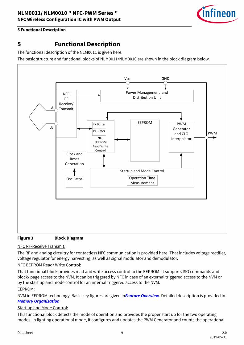
5 Functional DescriptionThe functional description of the NLM0011 is given here.The basic structure and functional blocks of NLM0011/NLM0010 are shown in the block diagram below.
LA
LB
Power Management and Distribution Unit
EEPROM
NFC EEPROM
Read Write Control
PWMGeneratorand CLO
InterpolatorPWM
Startup and Mode Control
Clock and Reset
Generation
Oscillator
VCC GND
NFCRF
Receive/Transmit
Rx Buffer
Tx Buffer
Operation Time Measurement
Figure 3 Block Diagram
NFC RF-Receive Transmit:The RF and analog circuitry for contactless NFC communication is provided here. That includes voltage rectifier,voltage regulator for energy harvesting, as well as signal modulator and demodulator.NFC EEPROM Read/ Write Control:That functional block provides read and write access control to the EEPROM. It supports ISO commands andblock/ page access to the NVM. It can be triggered by NFC in case of an external triggered access to the NVM orby the start up and mode control for an internal triggered access to the NVM.EEPROM:NVM in EEPROM technology. Basic key figures are given inFeature Overview. Detailed description is provided in Memory OrganizationStart up and Mode Control:This functional block detects the mode of operation and provides the proper start up for the two operatingmodes. In lighting operational mode, it configures and updates the PWM Generator and counts the operational
NLM0011/ NLM0010 " NFC-PWM Series "NFC Wireless Configuration IC with PWM Output
5 Functional Description
Datasheet 9 2.02019-05-31

hours. It updates the NVM by operational hours periodically or if the chip underruns a undervoltage emergencythreshold limit. It interpolates the CLO setting as well, according to the configured aged function . Theinterpolation result changes the PWM frequency and duty cycle parameter dynamically, which are delivered tothe PWM generator. In configuration mode it provides NFC reader access to the NVM and responds to NFCreader commands. It is implemented as a hard coded finite state machine.PWM Generator and CLO Interpolator:That functional block is configured by the start up and mode control with the PWM period and duty cyclesetting. It is only active in lighting operational mode and generates the PWM output according to configurationand CLO until the chip is switched off (CLO function is only available in NLM0011).Power Management and Distribution:This unit includes the voltage regulators and under voltage lockout detection and control function. The chip caneither be supplied by energy harvested from the NFC field or by an external VCC source. In case an externalVCCsource is present the NLM0011 chip enters the lighting operational mode and no NFC operation incl. energyharvesting is possible anymore.Clock and Reset Generation/ Oscillator:Internal clocks and resets are generated here. Architectural clock gating control is done as well. In configurationmode the clock of 13,56 MHz is derived from the external NFC carrier by a clock recovery unit within the NFCTransceiver. In lighting operational mode the clock is provided by internal oscillator running at 27,12MHz.
NLM0011/ NLM0010 " NFC-PWM Series "NFC Wireless Configuration IC with PWM Output
5 Functional Description
Datasheet 10 2.02019-05-31

6 Memory OrganizationThe EEPROM structure and Organization is described here.In general the EEPROM memory is organized in 18 blocks each with a block size of 4 byte. Blocks 00Hh to 0CH arefreely available for user and application data. Blocks 0DH to 11H are used to store chip configuration andindividualization data.
3 2 1 0
Bit[31:24] Bit[23:16] Bit[15:8] Bit[7:0]
Byte and Bit Index of a block
Block address
Block Lock Information (2 bits per block)11H
Service Data10H
0FH
UID[63:32]0EH
UID[31:0]0DH
Service Area AFI Service Data
Application and User
Area
0CH
0BH
...
01H
00H
Application and User Data
Application and User Data
Application and User Data
Application and User Data
Application and User Data
Figure 4 General Memory Structure
In NLM0011/ NLM0010 product the EEPROM is utilized as follows:The UID Structure 0EH/ 0DH
The UID record contains the User Identification data, which is defined by the ISO/ IEC standard and Infineon.
Table 2 UID Block 0EH
Bit index of UID / Description
[63:56] [55:48] [47:40] [39:32]
ISO E0H ISO IFX 05H Family Code Byte UID[39:32]
Table 3 UID Block 0DH
Bit index of UID / Description
[31:0]
UID[31:0]
NLM0011/ NLM0010 " NFC-PWM Series "NFC Wireless Configuration IC with PWM Output
6 Memory Organization
Datasheet 11 2.02019-05-31

Table 4 UID Fields Description
Abbreviation Description
ISO According to ISO/IEC 18000-3 mode 1 fixed to E0H
ISO IFX According to ISO/IEC 7816-6 the IC Manufacturer Code (IC Mfg code)is assignedto 05H.
Family Code Byte Identification within the NLM0011/NLM0010 product family, the value is :• B8H for product NLM0011 (design steps A11, A12, A13)• B9H for product NLM0011(design step A14)• B0H for product NLM0010 (design steps A11, A12, A13)• B1H for product NLM0010(design step A14)for the NLM0011/NLM0010 Version 1.0
Following table defines the coding for the Family Code byte of the UID (bit 47 - bit 40):
Table 5 Family Code Byte
Bit index of UID / Description
[47:45] [44] [43:40]
Memory Size and MemoryIdentification:The 576-Bit EEPROM is identified by thefixed value 101B
Type Identifier:It is fixed to 1B forNLM0011/NLM0010.
Chip Type:NLM0011 is identified by 1xxxB
NLM0010 is identified by 0xxxB
The UID field UID[39:0] is reserved to store Infineon specific manufacturing information.The Lock Block 11H
Memory block 11H contains the information to protect an individual block in the memory against overwriting.The structure of this block is described in following table.
Table 6 Lock Block 11H
Bit index of block 11H Description
[31:30] Lock information for block 0FH.10B the block can be read and written,others the block is protected against write access (read only)
[29:28] Lock information for block 0EH.10B the block can be read and written,others the block is protected against write access (read only)
[27:26] Lock information for block 0DH.10B the block can be read and written,others the block is protected against write access (read only)
[25:24] Lock information for block 0CH.10B the block can be read and written,others the block is protected against write access (read only)
[23:22] Lock information for block 0BH.10B the block can be read and written,
NLM0011/ NLM0010 " NFC-PWM Series "NFC Wireless Configuration IC with PWM Output
6 Memory Organization
Datasheet 12 2.02019-05-31

Table 6 Lock Block 11H (continued)
Bit index of block 11H Description
others the block is protected against write access (read only)
[21:20] Lock information for block 0AH.10B the block can be read and written,others the block is protected against write access (read only)
[19:18] Lock information for block 09H.10B the block can be read and written,others the block is protected against write access (read only)
[17:16] Lock information for block 08H.10B the block can be read and written,others the block is protected against write access (read only)
[15:14] Lock information for block 07H.10B the block can be read and written,others the block is protected against write access (read only)
[13:12] Lock information for block 06H.10B the block can be read and written,others the block is protected against write access (read only)
[11:10] Lock information for block 05H.10B the block can be read and written,others the block is protected against write access (read only)
[9:8] Lock information for block 04H.10B the block can be read and written,others the block is protected against write access (read only)
[7:6] Lock information for block 03H.10B the block can be read and written,others the block is protected against write access (read only)
[5:4] Lock information for block 02H.10B the block can be read and written,others the block is protected against write access (read only)
[3:2] Lock information for block 01H.10B the block can be read and written,others the block is protected against write access (read only)
[1:0] Lock information for block 00H.10B the block can be read and written,others the block is protected against write access (read only)
The initial value of this block is 02 AA AA AAH, which indicates that block 0FH and the UID are protected againstoverwriting.Issuing a WriteBlock or a WriteByte command to block 11H performs a write cycle to the memory. The onlypossible transition is 1 to 0 for each bit of this block. Therefore, unlocking of a block is not possible.
NLM0011/ NLM0010 " NFC-PWM Series "NFC Wireless Configuration IC with PWM Output
6 Memory Organization
Datasheet 13 2.02019-05-31

The change of lock information must be executed as a “Read-Modify-Write” operation. Firstly the block must beread, then all appropriate bits have to be changed, and finally the information should be written back to theblock. The write operation should be performed in a secure environment.Note: Changing bits from ’0’ to ’1’ will lead to unexpected chip behavior and should not be performed. Theresponse to a write command including incorrect changed bits is not valid.Example:Assuming a NLM0011/ NLM0010 chip, which has not been configured in any way, the Lock Block (11H) containsdata 02 AA AA AAH (i.e. only block 0FH and UID are write protected).To lock i.e. block 06H from being re-written, the following operations should be performed in a secureenvironment. The command example includes the ISO Flags and the CRC:• Read content of block 11H with “Read single block” command
- Command example for read single block 02 20 11 4F 51H
- Response 00 AA AA AA 02 D4 BCH
- Memory content of block 11H is 02 AA AA AAH
• Modify bits [13:12] to 00B
- Result is 02 AA 8A AAH
• Write modified value to block 11H with “Write single block” command- Command example for write single block 02 21 11 AA 8A AA 02 1C F5H
- Acknowledge Response 00 78 F0H
- Memory content of block 11H is now 02 AA 8A AAH
After this sequence, block 06H is locked and cannot be changed anymore.The Service Block 10H
Block 10H can only be written with the WriteByte command. Bits [31:24] and bits [23:20] are writable, the rest ofblock 10H is read only.
Table 7 Service Block 10H
Bit Index Abbreviation Description
[31:24] RFI Reserved for Infineon
[23:22] AFILOCK These two bits are internally used to lock the AFI byte.10BAFI byte is writable00BAFI is locked
[21:20] LOCK These two bits are used to lock Byte 3 of page 10H.10BByte 3 (bit(31:24)) are writable00HByte 3 (bit(31:24)) bit are read only
[19:0] Configuration Data Used by Infineon for chip configuration
AFI Block 0FH
Block 0FH holds the AFI Byte in bit [31:24]. This byte can only be written using the WriteAFI command. This blockis write only.Note:Writing the AFI with the WriteAFI command should be performed in a secure environment.
NLM0011/ NLM0010 " NFC-PWM Series "NFC Wireless Configuration IC with PWM Output
6 Memory Organization
Datasheet 14 2.02019-05-31
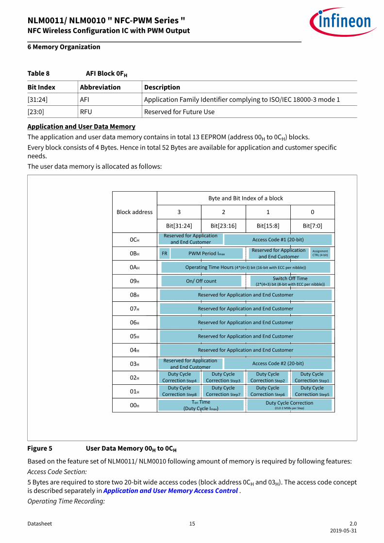
Table 8 AFI Block 0FH
Bit Index Abbreviation Description
[31:24] AFI Application Family Identifier complying to ISO/IEC 18000-3 mode 1
[23:0] RFU Reserved for Future Use
Application and User Data MemoryThe application and user data memory contains in total 13 EEPROM (address 00H to 0CH) blocks.Every block consists of 4 Bytes. Hence in total 52 Bytes are available for application and customer specificneeds.The user data memory is allocated as follows:
3 2 1 0
Bit[31:24] Bit[23:16] Bit[15:8] Bit[7:0]
Byte and Bit Index of a block
Block address
0CH
0BH
02H
01H
00H
0AH
09H
08H
07H
06H
05H
04H
03H
Duty Cycle Correction Step5
Duty Cycle Correction Step6
Duty Cycle Correction Step7
Duty Cycle Correction Step8
Reserved for Application and End Customer
Reserved for Application and End Customer
Reserved for Application and End Customer
Reserved for Application and End Customer
Reserved for Application and End Customer
Operating Time Hours (4*(4+3) bit (16-bit with ECC per nibble))
Access Code #1 (20-bit)
Switch Off Time(2*(4+3) bit (8-bit with ECC per nibble))
Reserved for Application and End CustomerPWM Period Imax
On/ Off count
Duty Cycle Correction Step1
Duty Cycle Correction Step2
Duty Cycle Correction Step3
Duty Cycle Correction Step4
Ton Time(Duty Cycle Imax)
Duty Cycle Correction(CLO 2 MSBs per Step)
Access Code #2 (20-bit)
Reserved for Application and End Customer
Reserved for Application and End Customer
Assignment CTRL (4-bit)FR
Figure 5 User Data Memory 00H to 0CH
Based on the feature set of NLM0011/ NLM0010 following amount of memory is required by following features:Access Code Section:5 Bytes are required to store two 20-bit wide access codes (block address 0CH and 03H). The access code conceptis described separately in Application and User Memory Access Control .Operating Time Recording:
NLM0011/ NLM0010 " NFC-PWM Series "NFC Wireless Configuration IC with PWM Output
6 Memory Organization
Datasheet 15 2.02019-05-31

The operating time is stored as a 16-Bit integer value and updated by increment value every 4 hours ofoperation. Therefore the number of operating hours corresponds to the 16-Bit integer value multiplied by four.The 16-bit word consists of 4 nibbles. Every nibble contains a 3-bit ECC check sum. The ECC is able to detect andcorrect a single bit error within the nibble, in case the value is falsified within the NVM. The ECC is also able todetect two bit errors, but cannot correct them properly. Hence 28-bits are required to store the operating time(4 data nibbles with 3 additional ECC-bits: 4*7bit=28 bit). The 28-bit value is stored at address 0AH.Furthermore the current time, when the device is powered off need to be stored. This is an offset time to the 16-bit value of operating hours. This time offset has a value of 0 hours to 4 hours. It is stored in one byte, where thetwo most significant bits represent the time offset in hours and the 6 low significant bits represent the timeoffset in minutes. This byte consists of two nibbles, where every nibble is protected by 3 additional ECC checkbits. Hence 2*(4+3) bits (→ 14-bits) are required to store the offset time at switch off event.In case of switch off the power the On/off counter is incremented and the value is stored (16-bit). Switch offTime and on/off counter are located at address 09H.Constant Lumen Output (CLO):The User Memory needs to store the value of the PWM period and the PWM duty cycle of 100% current set point.Both values are given as 15-Bit integer numbers. The bit "FR" defines the slope of the CLO function.Furthermore the CLO table setting points need to be stored. Up to eight setting points are required. One byte isrequired per setting point. The 4 most significant bits are used to store the time information (means operationtime reference point as multiples of 8192 hours), the 4 low significant bits are used to store the four lowsignificant bits of duty cycle offset information in percent to 50%. Two additional bytes are required to store themost significant bit per duty cycle and step (to achieve full resolution of 50% offset). The duty cycle offset isinternally processed as parts of 128. No redundancy need to be provided for these parameters, since they arerarely written.So in total 12 Bytes are required to configure the PWM according to the CLO table.Additional Memory:24 additional bytes are available for application and end user specific purposes (read- and writable).
NLM0011/ NLM0010 " NFC-PWM Series "NFC Wireless Configuration IC with PWM Output
6 Memory Organization
Datasheet 16 2.02019-05-31
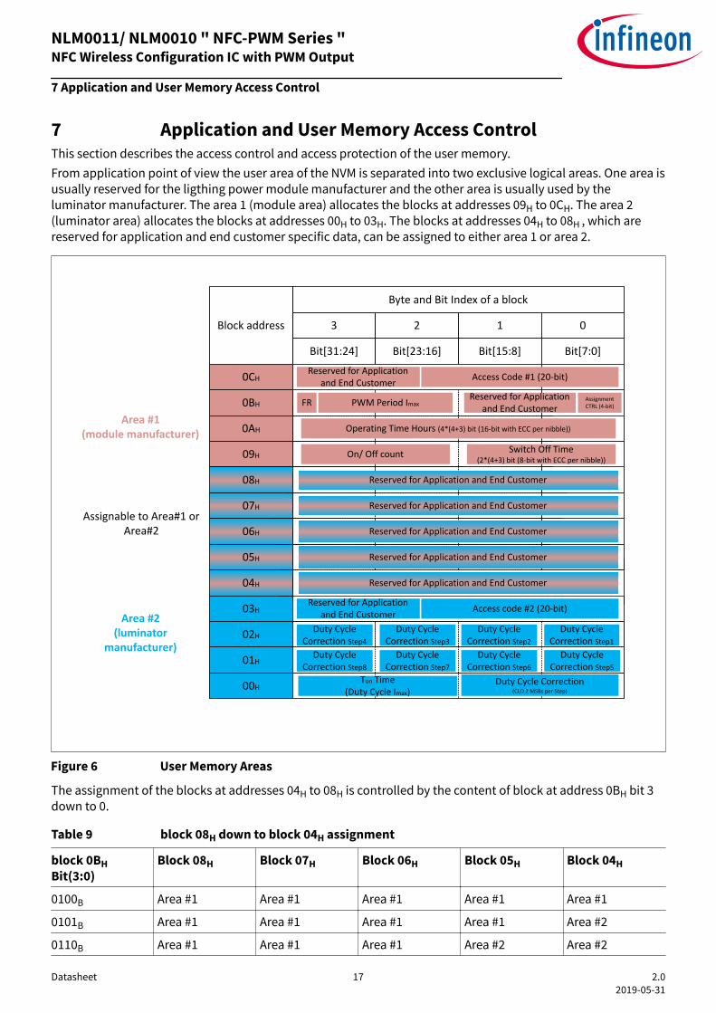
7 Application and User Memory Access ControlThis section describes the access control and access protection of the user memory.From application point of view the user area of the NVM is separated into two exclusive logical areas. One area isusually reserved for the ligthing power module manufacturer and the other area is usually used by theluminator manufacturer. The area 1 (module area) allocates the blocks at addresses 09H to 0CH. The area 2(luminator area) allocates the blocks at addresses 00H to 03H. The blocks at addresses 04H to 08H , which arereserved for application and end customer specific data, can be assigned to either area 1 or area 2.
3 2 1 0
Bit[31:24] Bit[23:16] Bit[15:8] Bit[7:0]
Byte and Bit Index of a block
Block address
0CH
0BH
02H
01H
00H
0AH
09H
08H
07H
06H
05H
04H
03H
Duty Cycle Correction Step5
Duty Cycle Correction Step6
Duty Cycle Correction Step7
Duty Cycle Correction Step8
Reserved for Application and End Customer
Reserved for Application and End Customer
Reserved for Application and End Customer
Reserved for Application and End Customer
Access code #2 (20-bit)
Reserved for Application and End Customer
Operating Time Hours (4*(4+3) bit (16-bit with ECC per nibble))
Access Code #1 (20-bit)
Switch Off Time(2*(4+3) bit (8-bit with ECC per nibble))
Reserved for Application and End CustomerPWM Period Imax
On/ Off count
Duty Cycle Correction Step1
Duty Cycle Correction Step2
Duty Cycle Correction Step3
Duty Cycle Correction Step4
Ton Time(Duty Cycle Imax)
Area #1(module manufacturer)
Area #2(luminator
manufacturer)
Duty Cycle Correction(CLO 2 MSBs per Step)
Assignable to Area#1 or Area#2
Reserved for Application and End Customer
Reserved for Application and End Customer
Assignment CTRL (4-bit)FR
Figure 6 User Memory Areas
The assignment of the blocks at addresses 04H to 08H is controlled by the content of block at address 0BH bit 3down to 0.
Table 9 block 08H down to block 04H assignment
block 0BHBit(3:0)
Block 08H Block 07H Block 06H Block 05H Block 04H
0100B Area #1 Area #1 Area #1 Area #1 Area #1
0101B Area #1 Area #1 Area #1 Area #1 Area #2
0110B Area #1 Area #1 Area #1 Area #2 Area #2
NLM0011/ NLM0010 " NFC-PWM Series "NFC Wireless Configuration IC with PWM Output
7 Application and User Memory Access Control
Datasheet 17 2.02019-05-31
Table 9 block 08H down to block 04H assignment (continued)
block 0BHBit(3:0)
Block 08H Block 07H Block 06H Block 05H Block 04H
0111B Area #1 Area #1 Area #2 Area #2 Area #2
1000B Area #1 Area #2 Area #2 Area #2 Area #2
1001B Area #2 Area #2 Area #2 Area #2 Area #2
others Area #1 Area #1 Area #1 Area #1 Area #1
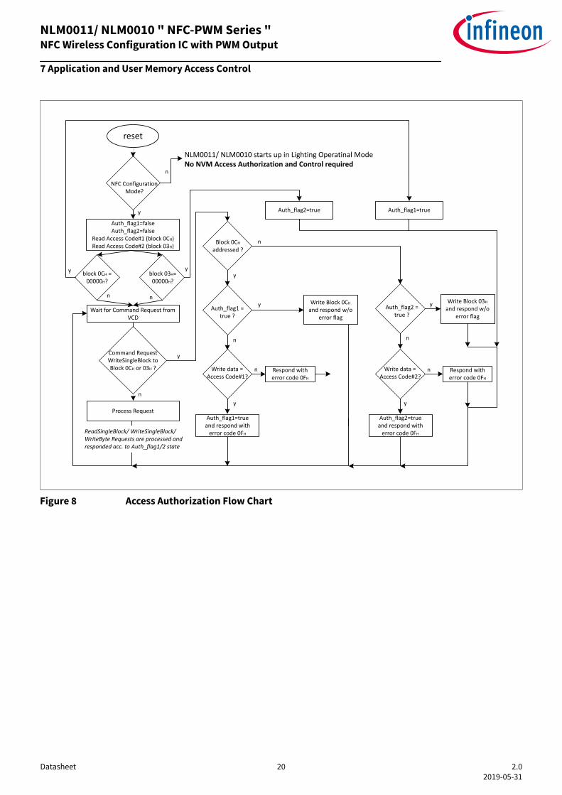
In NFC configuration mode, it is required to control the access of the two areas and to prevent unauthorizedaccess into an area. Therefore two access codes are defined. The access codes are located in the blocks 0CH and03H.The authorization concept can be described like that (the VICC is the NLM0011/ NLM0010 chip herein and theVCD is the NFC Reader herein):• VCD has to identify and authorize itself by providing an access code to the VICC• Two access codes are stored in the NVM
- Area 1 access code at block 0CH
- Area 2 access code at block 03H
• VCD provides an access code request (transmits an access code) to VICC• VICC compares the received access code with the stored access code
- In case of Match: memory access is authorized from now (as long as VICC does not change into power-off state)
- In case of No Match: memory access is not authorized• Authorized Memory Access Means:
- Read Access:- NFC requests ReadSingleBlock are served and responded by the VICC by providing the read data of
the requested NVM block , except Block 0CH/ 03H
- Read rights in both Area 1 and Area 2 (no matter which of the two access codes are used) aregiven
- ReadSingleBlock request to block 0CH or 03H: The VICC will not send back the content of theblock to VCD. The value 00000000H will always be returned back instead of.
- Write Access:- NFC requests WriteSingleBlock/Write Byte are served and responded by the VICC regular , if
Authorization with Access Code #1 was done (complete user memory area can be written)- In case the Authentication was done with Access Code #2 and no Authentication with Access Code
#1 was done, write access only possible to area #2 ( luminator area)• Non Authorized memory access (and read access to block at address 0CH/ 03H when authorized) means:
- If a ReadSingleBlock request by VCD is not authorized: The VICC responds to the ReadSingleBlockrequest by non error read response and data value 00000000H.
- If a WriteSingleBlock request by VCD is not authorized: The VCC responds with error response and errorcode 0FH
NLM0011/ NLM0010 " NFC-PWM Series "NFC Wireless Configuration IC with PWM Output
7 Application and User Memory Access Control
Datasheet 18 2.02019-05-31

SOF Flags00H
00000000H CRC EOF
Response to ReadSingleBlock Request (Read access not authorized):
Response to ReadSingleBlock Request to block 0CH/03H (Read access authorized):
SOF Flags00H
00000000H CRC EOF
Response to WriteSingleBlock or WriteByte Request (Write access not authorized):
SOF Flags CRC EOFError Code
0FH
Figure 7 Access controlled responses
The authorization procedure is defined as follows:
NLM0011/ NLM0010 " NFC-PWM Series "NFC Wireless Configuration IC with PWM Output
7 Application and User Memory Access Control
Datasheet 19 2.02019-05-31
NFC Configuration Mode?
n
NLM0011/ NLM0010 starts up in Lighting Operatinal ModeNo NVM Access Authorization and Control required
y
Auth_flag1=falseAuth_flag2=false
Read Access Code#1 (block 0CH)Read Access Code#2 (block 03H)
Wait for Command Request from VCD
Process Request
n
Block 0CH addressed ?
Auth_flag1 = true ?
n
Write data =Access Code#1?
y
y
y
n
Auth_flag2 = true ?
y
n
Write data =Access Code#2?
y
n n
ReadSingleBlock/ WriteSingleBlock/ WriteByte Requests are processed and responded acc. to Auth_flag1/2 state
Respond with error code 0FH
Auth_flag1=trueand respond with
error code 0FH
Auth_flag2=trueand respond with
error code 0FH
Respond with error code 0FH
Write Block 0CH
and respond w/o error flag
Write Block 03H
and respond w/o error flag
Command RequestWriteSingleBlock to Block 0CH or 03H ?
n
Auth_flag2=true
y
yblock 0CH =00000H?
block 03H=00000H?
n
Auth_flag1=true
y
reset
y
Figure 8 Access Authorization Flow Chart
NLM0011/ NLM0010 " NFC-PWM Series "NFC Wireless Configuration IC with PWM Output
7 Application and User Memory Access Control
Datasheet 20 2.02019-05-31

8 NLM0011/NLM0010 EEPROM Shipment Content (Infineon toCustomer)
User memory Delivery content (NLM0011 - product with CLO):
3 2 1 0
Bit[31:24] Bit[23:16] Bit[15:8] Bit[7:0]
Byte and Bit Index of a block
Block address
0CH
0BH
02H
01H
00H
0AH
09H
08H
07H
06H
05H
04H
03H
F4HF5HF6HF7H
55555555H
55555555H
AAAAAAAAH
AAAAAAAAH
00000H
55555555H
00000000H
00000H
0000H
000H03E8H
0000H
F0HF1HF2HF3H
0065H
Area #1(module manufacturer)
Area #2(luminator
manufacturer)
FFFFH
Assignable to Area#1 or Area#2
000H
000H
0H
Figure 9 EEPROM Delivery Content User Memory with CLO
User memory Delivery content (NLM0010 - product w/o CLO):
NLM0011/ NLM0010 " NFC-PWM Series "NFC Wireless Configuration IC with PWM Output
8 NLM0011/NLM0010 EEPROM Shipment Content (Infineon to Customer)
Datasheet 21 2.02019-05-31

3 2 1 0
Bit[31:24] Bit[23:16] Bit[15:8] Bit[7:0]
Byte and Bit Index of a block
Block address
0CH
0BH
02H
01H
00H
0AH
09H
08H
07H
06H
05H
04H
03H
F4HF5HF6HF7H
55555555H
55555555H
AAAAAAAAH
AAAAAAAAH
00000H
55555555H
00000000H
00000H
0000H
000H03E8H
0000H
F0HF1HF2HF3H
0065H
Area #1(module manufacturer)
Area #2(luminator
manufacturer)
FFFFH
Assignable to Area#1 or Area#2
000H
000H
0H
Blocks 02H and 01H are locked
Figure 10 EEPROM Delivery Content User Memory without CLO
UID Content (Block 0EH and 0DH): content according to UID Description in chapter Memory Organization.For product without enabled CLO function (NLM0010), the family code byte is set to B1H.For product with enabled CLO function (NLM0011), the family code byte is set to B9H.Service Data (Block 10H and 0FH): content according to Service Data Description in chapter MemoryOrganization.In block 0FH the AFI byte is written by value 00H for all NFC PWM series related products. All bits, which arereserved for future use, are written by value 0B.Block Lock Information (Block 11H):For the product with enabled CLO feature all blocks of the user data area are read- and write-able. For theproduct without CLO feature the blocks 01H and 02H are permanently locked .The UID (blocks 0EH and block 0DH) is locked. The blocks 0FH and 10H are locked as well.The parameters PWM Period Imax (Block 0BH Bit (30:16)) and Duty Cycle Imax(Block 00HBit(31:16)) are initiallyprogrammed to 27,12kHz(value 03E8H) and 10 % (value 0065H). The bit 31 of Block 0BH"FR" has to beprogrammed to 0B(non inverting PWM output).
NLM0011/ NLM0010 " NFC-PWM Series "NFC Wireless Configuration IC with PWM Output
8 NLM0011/NLM0010 EEPROM Shipment Content (Infineon to Customer)
Datasheet 22 2.02019-05-31
9 Constant Lumen Output (CLO) and Operating TimeCounting (OTC)
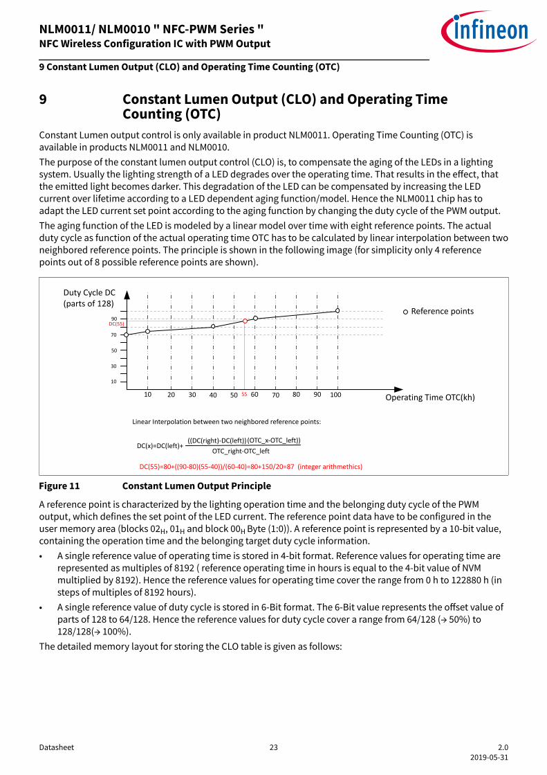
Constant Lumen output control is only available in product NLM0011. Operating Time Counting (OTC) isavailable in products NLM0011 and NLM0010.The purpose of the constant lumen output control (CLO) is, to compensate the aging of the LEDs in a lightingsystem. Usually the lighting strength of a LED degrades over the operating time. That results in the effect, thatthe emitted light becomes darker. This degradation of the LED can be compensated by increasing the LEDcurrent over lifetime according to a LED dependent aging function/model. Hence the NLM0011 chip has toadapt the LED current set point according to the aging function by changing the duty cycle of the PWM output.The aging function of the LED is modeled by a linear model over time with eight reference points. The actualduty cycle as function of the actual operating time OTC has to be calculated by linear interpolation between twoneighbored reference points. The principle is shown in the following image (for simplicity only 4 referencepoints out of 8 possible reference points are shown).
Operating Time OTC(kh)
Duty Cycle DC (parts of 128)
10 20 30 40 50 60 70 80 90 100
10
30
50
70
90
55
DC(55)
Linear Interpolation between two neighbored reference points:
DC(x)=DC(left)+OTC_right-OTC_left
(OTC_x-OTC_left))((DC(right)-DC(left))
DC(55)=80+((90-80)(55-40))/(60-40)=80+150/20=87 (integer arithmethics)
Reference points
Figure 11 Constant Lumen Output Principle
A reference point is characterized by the lighting operation time and the belonging duty cycle of the PWMoutput, which defines the set point of the LED current. The reference point data have to be configured in theuser memory area (blocks 02H, 01H and block 00H Byte (1:0)). A reference point is represented by a 10-bit value,containing the operation time and the belonging target duty cycle information.• A single reference value of operating time is stored in 4-bit format. Reference values for operating time are
represented as multiples of 8192 ( reference operating time in hours is equal to the 4-bit value of NVMmultiplied by 8192). Hence the reference values for operating time cover the range from 0 h to 122880 h (insteps of multiples of 8192 hours).
• A single reference value of duty cycle is stored in 6-Bit format. The 6-Bit value represents the offset value ofparts of 128 to 64/128. Hence the reference values for duty cycle cover a range from 64/128 (→ 50%) to128/128(→ 100%).
The detailed memory layout for storing the CLO table is given as follows:
NLM0011/ NLM0010 " NFC-PWM Series "NFC Wireless Configuration IC with PWM Output
9 Constant Lumen Output (CLO) and Operating Time Counting (OTC)
Datasheet 23 2.02019-05-31

DC8(5:4)
DC7(5:4)
DC6(5:4)
DC5(5:4)Duty Cycle Imax
OTC1 (3:0)DC1(3:0)OTC2(3:0)DC2(3:0)OTC3(3:0)DC3(3:0)OTC4(3:0)DC4(3:0)
OTC8 (3:0)DC8(3:0) OTC5(3:0)DC5(3:0)OTC5(3:0)DC6(3:0)OTC7(3:0)DC7(3:0)Block 01H
Block 02H
Bit0Bit8Bit16Bit24 Bit8Bit15Bit23Bit31Byte0Byte1Byte2Byte3
DC4(5:4)
DC3(5:4)
DC2(5:4)
DC1(5:4)Block 00H
Figure 12 CLO Table Memory Layout
Example:The following example describes, how to calculate the 10-bit reference value of a particular referencepoint to be stored in the NVM. Let's assume a reference point at an operating time of 66000 hours and a targetduty cycle of 82% of the duty cycle definition of Imax (value of block 00H, Byte(3:2)):• The 4-bit value of operating time OTC : → 66000/8192=8,06 → integer rounding 8 → 1000B
• The 6-bit value of duty cycle:- Convert the given percentage value into parts of 128: → 82/100=X/128 → X=104,96 → integer rounding
105- Calculate the offset to 64 parts of 128: → 105-64=41 → 101001B
The NLM0011/ NLM0010 chip is continuously counting the operation time and is continuously interpolating theresulting duty cycle. The interpolation result is then multiplied with the value of Duty Cycle Imax (value of block00H, Byte(3:2)) and this product is then divided by 128. This value is then used by the PWM generator andgenerates a PWM signal of frequency PWM period IMax (value of block 0BH, Byte(3:2)) with the calculated dutycycle.Monotonous falling CLO curves are supported in NLM0011 in chip version A14 (indicated by family code bytevalue B9H).In order to enable a falling CLO curve the Bit "FR" (bit 31 of NVM block address 0BH) has to beprogrammed to value 1B (for rising CLO curves the default 0B has to be used. In case of falling CLO curve thecovered CLO range is 64 parts of 128 down to 0 of duty cycle Imax (for rising CLO curve the covered range is 64parts of 128 to 128 parts of 128 of duty cycle Imax).The reference point duty cycle value for a falling CLO curve has to be entered as :CLO reference point (falling curve) = 64 - <desired value (0...64)>Example:
Table 10 CLO Duty Cycle Reference values
reference point number desired value (parts of 128 ofDuty Cycle Imax)
CLO table value
Step 1 64 0
Step 2 56 8
Step 3 42 22
Step 4 31 33
Step 5 27 37
Step 6 19 45
Step 7 13 51
NLM0011/ NLM0010 " NFC-PWM Series "NFC Wireless Configuration IC with PWM Output
9 Constant Lumen Output (CLO) and Operating Time Counting (OTC)
Datasheet 24 2.02019-05-31

Table 10 CLO Duty Cycle Reference values (continued)
reference point number desired value (parts of 128 ofDuty Cycle Imax)
CLO table value
Step 8 3 61
Note: Only strict monotonous falling or rising CLO curves are supported.
The operation time is counted and the NVM value of operation time (block 0AH) is incremented/ updated every 4hours. Hence the 16-bit value multiplied by four represents the operating time in hours. Once the value FFFFH isreached, the operating time counting stops and keeps the value FFFFH. The current operating time is saved intothe NVM with an accuracy of 30 seconds in case the external supply voltage VCC is switched off . Here theremainder time with respect to the last regular 4 hours update is stored (hours and minutes).Furthermore the number of power cycles is counted and stored in block 09H (Byte(3:2)). The value isincremented, when external supply voltage VCC is switched off.In order to save the housekeeping data into the NVM in case of switching off the external supply, the chipintegrates an under voltage lockout detection. An external capacitor on VCC is required to provide the requiredenergy for saving the housekeeping data in case of power off.The NVM Memory layout of the OTC related content looks like:
Block 0AH
Bit0Bit8Bit16Bit24 Bit7Bit15Bit23Bit31Byte0Byte1Byte2Byte3
0BC00C01D0C02D1D2D30BC10C11D4C12D5D6D70BC20C21D8C22D9D10D110BC30C31D12C32D13D14D15
D15-D0: 16 data bits of Operation Time Counter ValueCx0-Cx2: ECC check bits belonging to the respective nibble of OTC data
Bit0Bit8Bit16Bit24 Bit7Bit15Bit23Bit31Byte0Byte1Byte2Byte3
0BC00C01M0C02M1M2M30BC10C11M4C12M5H0H1On/ Off Count 16-BitBlock 09H
H1-H0: 2 bits (remainder time in hours)M5-M0: 6 bits (remainder time in minutes)Cx0-Cx2: ECC check bits belonging to the respective nibble of data
Figure 13 OTC related NVM content
Note: The OTC related content contains redundancy for error detection and correction (Bits Cxx). It is possible todetect and correct a single bit error per four data bits. In case the blocks 0AH or 09H are written by NFC the VCD hasto calculate the respective ECC check bits and to assemble the block content.
NLM0011/ NLM0010 " NFC-PWM Series "NFC Wireless Configuration IC with PWM Output
9 Constant Lumen Output (CLO) and Operating Time Counting (OTC)
Datasheet 25 2.02019-05-31

10 PWM OverviewThe NLM0011/NLM0010 is generating a pulse width modulated digital signal output. This PWM signal ischaracterized by its frequency , the duty cycle and the voltage swing.
TPWM
THigh
TLow
TPWM: Period of Pulse Width Modulation fPWM: Frequency of Pulse Width ModulationD: Duty Cycle of Pulse Width ModulationVDDP: Voltage Swing
D=(THigh/TPWM)100%fPWM=1/TPWM
VDDP
Figure 14 PWM Output Characteristics
The signal output is generated from an internal clock derived from an internal oscillator running at frequency of27,12 MHz.The length of period of the PWM signal TPWM is derived from the content of NVM block 0BH (Byte (3:2)). This 16-bit value represents the number of internal clock ticks, which are required to achieve the desired frequency.Example: If a PWM frequency of 25kHz ( → Period of 40us) is desired, then the NVM value needs to be 043DH(27120kHz/25kHz=1084,8 → rounded to 1085).The maximum value of THigh is derived from the content of NVM block 00H (Byte (3:2)). This 16-bit valuerepresents the number of internal clock ticks, which are required to achieve the desired logical HIGH outputtime. It represents as well the value of 100% Duty Cycle according to the constant lumen output table.Example: Referring to previous example: If a maximum duty cycle of 75% is desired, then the maximum high time is30us. Hence the NVM value needs to be 032EH (1085x0,75 = 813,75 → rounded to 814).The constant lumen output calculation unit of the NLM0011 chip finally adapts this value according to thecurrent interpolation result.Example: Referring to previous example: Lets assume the constant lumen output interpolation unit calculates acurrent duty cycle of 80% (or 102 parts of 128), then the effective current duty cycle will be 75*80%=60%.
NLM0011/ NLM0010 " NFC-PWM Series "NFC Wireless Configuration IC with PWM Output
10 PWM Overview
Datasheet 26 2.02019-05-31
11 NLM0011/ NLM0010 Command SetDescription of NLM0011 Command SetError CodesThe following ISO/IEC 18000-3 mode 1 compliant error codes are implemented in the NLM0011/ NLM0010:
Table 11 NLM0011 Error Codes
Error Code Meaning
01H The command is not supported
0FH Error with no specific information given or a specific error code is not supported.
10H The specified block is not available (does not exist).
12H The specified block is locked and cannot be changed (read only).
Invalid frame length handlingIf a command is sent to the NLM0011/ NLM0010 which has an invalid frame length no response is returned.Flag handlingThe NLM0011/NLM0010 ignores following flags. Commands are executed regardless of the state of these flagbits.• Protocol Extension flag• RFU flag• Option flag (special meaning only for Stay quiet, Select, Reset to ready and Inventory command)Command SetThe following command set is supported:
Table 12 NLM0011/NLM0010 Command Set
Available Commands Command Type )** Available Modes )**
Inventory M U
Stay quiet (state storage in state recovery) M A
Read single block O A/S/U
Write single block O A/S/U
Select O A
Reset to ready O A/S/U
Write AFI O A/S/U
Lock AFI O A/S/U
Write Byte C A/S/U
)* M … Mandatory; O … Optional; C … Custom)** A … Addressed; S … Selected; U … UnaddressedInventory (command code 01H)Implementation compliant to ISO/IEC 18000-3 mode 1.Note:For a masked inventory the number of mask bytes has to correspond to the length defined in the mask lengthfield.StayQuiet (command code 02H)Implementation based on ISO/IEC 18000-3 mode 1.
NLM0011/ NLM0010 " NFC-PWM Series "NFC Wireless Configuration IC with PWM Output
11 NLM0011/ NLM0010 Command Set
Datasheet 27 2.02019-05-31
Note:The NLM0011/NLM0010 responds after successful execution of the Stay Quiet command with set option_flagwith an acknowledge. The NLM0011/NLM0010 also responds with an acknowledge if the chip is already in Quietstate.
Table 13 Response Format for Stay Quiet command with set option_flag
SOF Flags CRC EOF
00H 16-Bit
This feature can be used to ensure that the addressed chip really could be set to the Quiet state. If the readerdoes not detect an acknowledge it can be assumed that the addressed chip is not present.ReadSingleBlock (command code 20H)Implementation compliant to ISO/IEC 18000-3 mode 1. Block 0FH is read protected. Reading this block results inan error response with error code 0FH. Sending the ReadSingleBlock command with set option_flag results inthe error code 01H(command not supported).WriteSingleBlock (command code 21H)Implementation compliant to ISO/IEC 18000-3 mode 1. The UID (block 0DH and 0EH), the Service block (block10H), the AFI byte (block 0FH) cannot be written with the Write Single Block command. The NLM0011/NLM0010returns the error code 12H. Sending the WriteSingleBlock command with set option_flag results in the errorcode 01H(command not supported).Select (command code 25H)Implementation compliant to ISO/IEC 18000-3 mode 1. A chip already in selected state will reply anacknowledge response (response value 00H) on a subsequent Select command.ResetToReady (command code 26H)Implementation based on ISO/IEC 18000-3 mode 1.Note:If the NLM0011/ NLM0010 is already in the Ready state, it will not respond to a subsequent ResetToReadycommand. With this feature a reader only detects chips in Quiet state and reset them to the Ready state.If the chip is in Quiet state it will respond to an unaddressed ResetToReady command and set its state to Ready.If a chip is in the Selected state, it will move to the Ready state after a ResetToReady command. TheResetToReady command must be issued with set select_flag. If the ResetToReady is issued unaddressed oraddressed, the chip will stay in Selected state and will not send a response as defined in ISO/IEC 18000-3 mode1.WriteAFI (command code 27H)Implementation compliant to ISO/IEC 18000-3 mode 1. Sending the WriteAFI command with set option_flagresults in the error code 01H (command not supported).LockAFI (command code 28H)Implementation compliant to ISO/IEC 18000-3 mode 1. Sending the LockAFI command with set option_flagresults in the error code 01H (command not supported).WriteByte (customcommand)ISO-Command code = A0H
NLM0011/ NLM0010 Embedded Command Code = 90H
The Write Byte command writes the data of the specified byte. In the case of successful programming the chipsends back an acknowledge build up by 3 bytes. If access conditions are set to read only the chip returns theerror code 12H (write protected block). For any other error, error code 0FH is returned.
NLM0011/ NLM0010 " NFC-PWM Series "NFC Wireless Configuration IC with PWM Output
11 NLM0011/ NLM0010 Command Set
Datasheet 28 2.02019-05-31

Table 14 WriteByte Request Format
SOF Flags CommandCode
Parameters Data CRC EOF
8-Bit A0H 05H; [UID] 90H ADDR0 00H Byte 8-Bit 16-Bit
Table 15 WriteByte Parameter Field
Code Description Comment
05H IC manufacturercode of Infineon
Mandatory
UID UID for addressedcommand
mandatory for set Addressed flag, not included for Selected orUnaddressed command
Table 16 WriteByte Data Field
Code Description Comment
90H command code forWriteByte
ADDR0 block address address range 00H ... 0CH and 11H
00H RFU
Byte byte address inblock
address range 0H ... 3H; bit [7..2] are ignored and shall be set to ’0’.
8-Bit byte data to bewritten
Response Format (no errors):
Table 17 WriteByte regular response
SOF Flags CRC EOF
00H 16-Bit
Response in case of Errors:
Table 18 WriteByte Error Response
SOF Flags Data CRC EOF
01H Error Code )* 16-Bit
)* The Error Code is defined according to ISO/IEC 18000-3 mode 1.Note:The WriteByte command to block 11H and to bytes 2 and 3 in block 10H should be performed as “Read-Modify-Write” operation and in a secure environment .As default the WriteByte command to the following memory location is not possible (write protected block):• UID block 0DH
• UID block 0EH
• AFI block 0FH
NLM0011/ NLM0010 " NFC-PWM Series "NFC Wireless Configuration IC with PWM Output
11 NLM0011/ NLM0010 Command Set
Datasheet 29 2.02019-05-31

• Service block 10H, byte 0 and 1; for byte 2 refer to Memory Map description• Additionally, service block 10H, byte 3 can only be written if it is not locked by block 10H bit (21:20).
NLM0011/ NLM0010 " NFC-PWM Series "NFC Wireless Configuration IC with PWM Output
11 NLM0011/ NLM0010 Command Set
Datasheet 30 2.02019-05-31

12 NLM0011/ NLM0010 Electrical CharacteristicsAbsolute Maximum Ratings
Table 19 Absolute Maximum Ratings
Parameter Symbol Values Unit Note or testconditionMin. Typ. Max.
Input peak voltage betweenLA-LB
VInpeak 3.6 VPeak
Absolute Maximum FieldStrength for indefiniteexposure without damage.The chip functionality can beaffected.
Habsmax 10 A/m Conditions:Tjoperating = 110°C
Absolute Maximum FieldStrength for exposure for upto 10 seconds withoutdamage. The chip is notguaranteed to function
Habsmax12 12 A/m Conditions:Tjoperating = 110°C
Input peak voltage at VCC VPeak 5.5 V
Storage Temperature TStorage -40 150 °C
Stresses above the maximum values listed here may cause permanent damage to the device. Exposure toabsolute maximum rating conditions for extended periods may affect device reliability, including EEPROM dataretention and erase/write endurance. Maximum ratings are absolute ratings. Exceeding only one of these valuesmay cause irreversible damage to the integrated circuit. This is a stress rating only and functional operation ofthe device at these or any other conditions above those indicated in the operational sections of this data sheetis not implied.Operational Conditions and Parameters
Table 20 Operational Conditions and Parameters
Parameter Symbol Values Unit Note or testconditionMin. Typ. Max.
external supply voltage range VCC 3.0 3.3 5.5 V
Operating field strength Habsmax 0.15 5 A/m According ISO/IEC18000-3 mode 1
Nominal terminal voltage(between LA and LB)
VACNOM 2.95 V
NLM0011/ NLM0010 " NFC-PWM Series "NFC Wireless Configuration IC with PWM Output
12 NLM0011/ NLM0010 Electrical Characteristics
Datasheet 31 2.02019-05-31

Table 20 Operational Conditions and Parameters (continued)
Parameter Symbol Values Unit Note or testconditionMin. Typ. Max.
Ambient Temperature inlighting operational mode
TJL -40 105 °C The ambienttemperature isdefined as thetemperature ofthe surface of thepackage.Permanentoperation at hightemperature(ambienttemperatureabove 90°C) couldimpact theproduct lifetime.In such case,please contractInfineon FAE toevaluate theapplicationprofile.
Ambient Temperature in NFCConfiguration mode
TNFC -20 85 °C The ambienttemperature isdefined as thetemperature ofthe surface of thepackage.
Frequency of PWM output fPWM 0.9 40 kHz measuredbetween tworising edges
Duty Cycle of PWM output D 0 100 % D=THigh/TPWM
Duty Cycle accuracy DACC 0.1 %
High Voltage of PWM Output VDDP_H 2.65 2.8 2.9 V Test Condition:Load 10uA; 25°C
Low Voltage of PWM Output VDDP_L 0 0.2 V Test Condition:Load 2mA; 25°C
Driving Strength of PWMOutput
IPWM 2 mA
Power Consumption inConfiguration Mode
PCM 2 mW ConfigurationMode (NFCOperation andNVM read/writeaccess)
Power Consumption inLighting Operating Mode
POM 3.3 5.6 mW LightingOperation Mode(PWM Generation,CLO, operatingtime recording);VCC=3.3V
NLM0011/ NLM0010 " NFC-PWM Series "NFC Wireless Configuration IC with PWM Output
12 NLM0011/ NLM0010 Electrical Characteristics
Datasheet 32 2.02019-05-31

Table 20 Operational Conditions and Parameters (continued)
Parameter Symbol Values Unit Note or testconditionMin. Typ. Max.
Resonance Capacitancebetween terminals LA and LB
Cchip 23.5 pF Conditions:TA = 25°C, VLaLb=1.6Vrms
Startup Time in Operationallighting mode
TStartup 15 ms Time between Vccpresent and firstPWM pulsegenerated
ESD Hardness VESD 2 kV Human BodyModel
EEPROM write/ erase cyclesper block
Wcycles 100000 @T=85°C
EEPROM Data Retention DR 10 years @T=25°C
EEPROM Failure Rate FREEPROM 20000 dpm @10 yearsRetention
VCC capacitor CVCC 22 μF
NLM0011/ NLM0010 " NFC-PWM Series "NFC Wireless Configuration IC with PWM Output
12 NLM0011/ NLM0010 Electrical Characteristics
Datasheet 33 2.02019-05-31

13 Package Outline
Applicable package
Product Package is PG-SOT23-5-1.
Package Drawing and Dimension
Figure 15 Package Outline PG-SOT23-5-1
Revision historyDocumentversion
Date ofrelease
Description of changes
1.2 11-09-2018 • added NLM0010 specific information
1.3 04-02-2019 • added Support of falling CLO curves
2.0 06-11-2019 • finalize electrical characteristics
NLM0011/ NLM0010 " NFC-PWM Series "NFC Wireless Configuration IC with PWM Output
13 Package Outline
Datasheet 34 2.02019-05-31

TrademarksAll referenced product or service names and trademarks are the property of their respective owners.
Edition 2019-05-31Published byInfineon Technologies AG81726 Munich, Germany © 2019 Infineon Technologies AGAll Rights Reserved. Do you have a question about anyaspect of this document?Email: [email protected] Document referenceIFX-dgp1564595904539
IMPORTANT NOTICEThe information given in this document shall in noevent be regarded as a guarantee of conditions orcharacteristics (“Beschaffenheitsgarantie”) .With respect to any examples, hints or any typical valuesstated herein and/or any information regarding theapplication of the product, Infineon Technologieshereby disclaims any and all warranties and liabilities ofany kind, including without limitation warranties ofnon-infringement of intellectual property rights of anythird party.In addition, any information given in this document issubject to customer’s compliance with its obligationsstated in this document and any applicable legalrequirements, norms and standards concerningcustomer’s products and any use of the product ofInfineon Technologies in customer’s applications.The data contained in this document is exclusivelyintended for technically trained staff. It is theresponsibility of customer’s technical departments toevaluate the suitability of the product for the intendedapplication and the completeness of the productinformation given in this document with respect to suchapplication.
WARNINGSDue to technical requirements products may containdangerous substances. For information on the typesin question please contact your nearest InfineonTechnologies office.Except as otherwise explicitly approved by InfineonTechnologies in a written document signed byauthorized representatives of Infineon Technologies,Infineon Technologies’ products may not be used inany applications where a failure of the product orany consequences of the use thereof can reasonablybe expected to result in personal injury