no slide titleusers.encs.concordia.ca/~asim/coen 451/lectures/w_9/nwell_process.pdftwin tub/double...
TRANSCRIPT
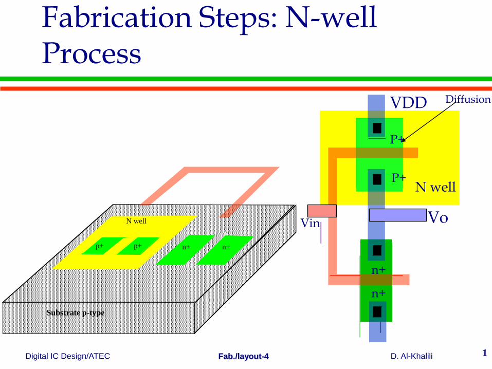
Digital IC Design/ATEC D. Al-Khalili Fab./layout-4 1
Fabrication Steps: N-well Process
Diffusion VDD
Vo
N well
P+
P+
n+
n+
Vin
p+
N well
p+ n+ n+ p+ p+
Substrate p-type
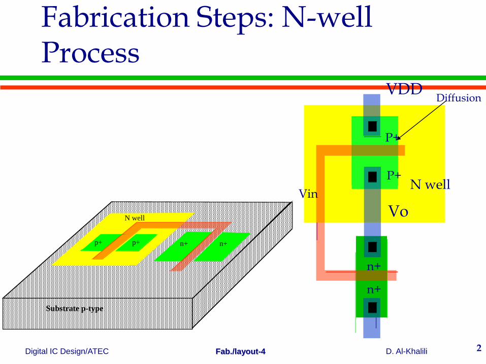
Digital IC Design/ATEC D. Al-Khalili Fab./layout-4 2
Fabrication Steps: N-well Process
Diffusion VDD
Vo
N well
P+
P+
n+
n+
Vin
p+
N well
p+ n+ n+ p+ p+
Substrate p-type
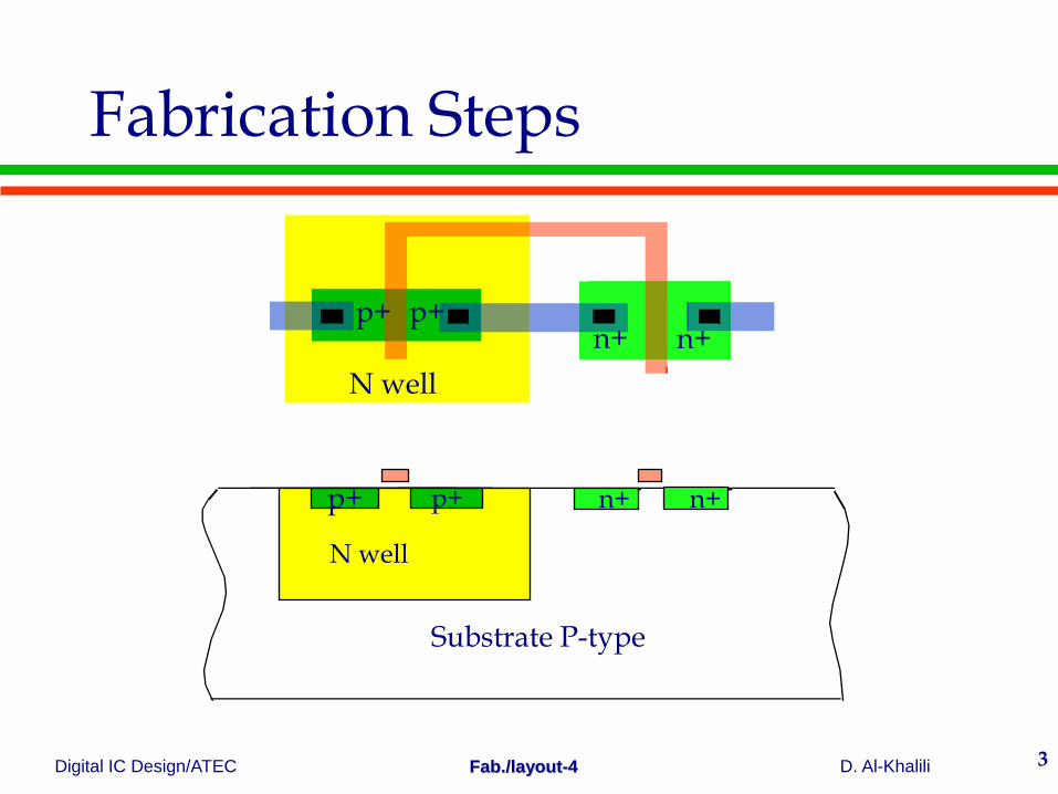
Digital IC Design/ATEC D. Al-Khalili Fab./layout-4 3
Fabrication Steps
p+ p+
N well
n+ n+
Substrate P-type
N well
p+ p+ n+ n+
Digital IC Design/ATEC D. Al-Khalili Fab./layout-4 4
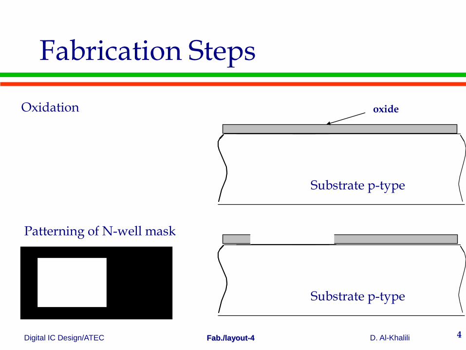
Fabrication Steps
Oxidation
Substrate p-type
Patterning of N-well mask
Substrate p-type
oxide
Digital IC Design/ATEC D. Al-Khalili Fab./layout-4 5
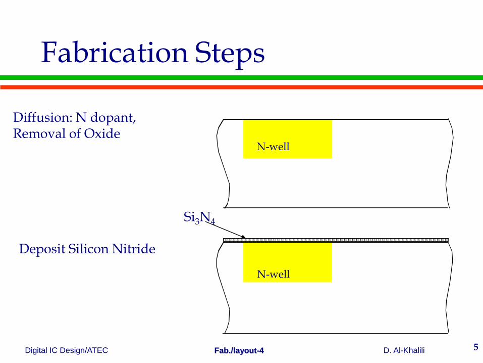
Fabrication Steps
Diffusion: N dopant, Removal of Oxide
Deposit Silicon Nitride
N-well
N-well
Si3N4
Digital IC Design/ATEC D. Al-Khalili Fab./layout-4 6
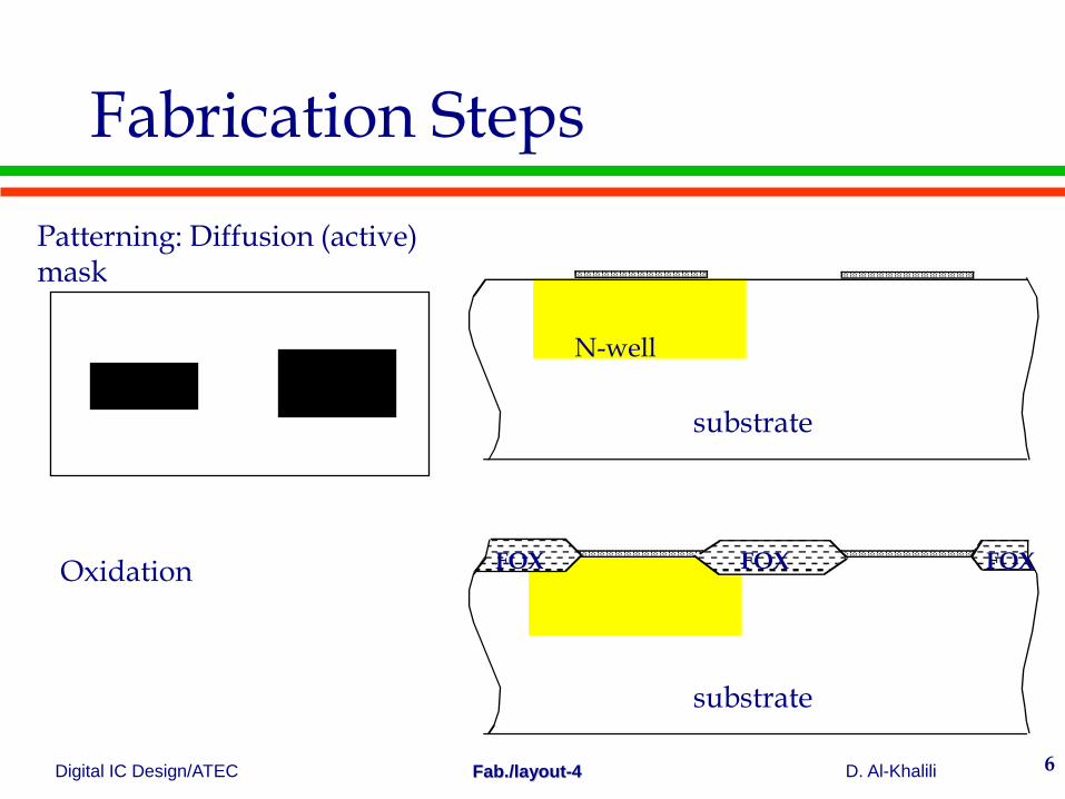
Fabrication Steps
Patterning: Diffusion (active) mask
Oxidation
N-well
substrate
FOX FOX FOX
substrate
Digital IC Design/ATEC D. Al-Khalili Fab./layout-4 7
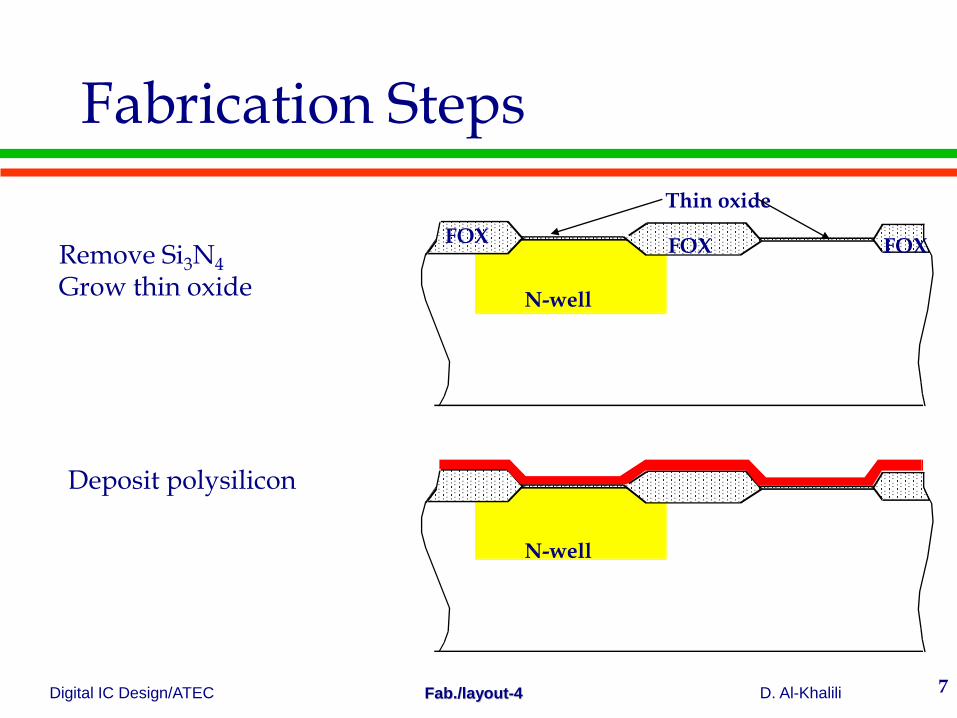
Fabrication Steps
Remove Si3N4 Grow thin oxide
Deposit polysilicon
N-well
N-well
FOX FOX FOX
Thin oxide
Digital IC Design/ATEC D. Al-Khalili Fab./layout-4 8
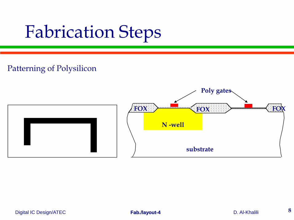
Fabrication Steps
Patterning of Polysilicon
FOX FOX FOX
N -well
Poly gates
substrate
Digital IC Design/ATEC D. Al-Khalili Fab./layout-4 9
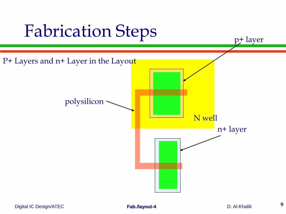
Fabrication Steps
P+ Layers and n+ Layer in the Layout
N well
p+ layer
n+ layer
polysilicon
Digital IC Design/ATEC D. Al-Khalili Fab./layout-4 10
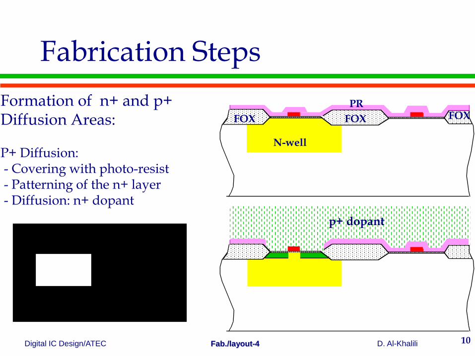
Fabrication Steps
Formation of n+ and p+ Diffusion Areas: P+ Diffusion: - Covering with photo-resist - Patterning of the n+ layer - Diffusion: n+ dopant
PR
FOX
N-well
FOX FOX
p+ dopant
Digital IC Design/ATEC D. Al-Khalili Fab./layout-4 11
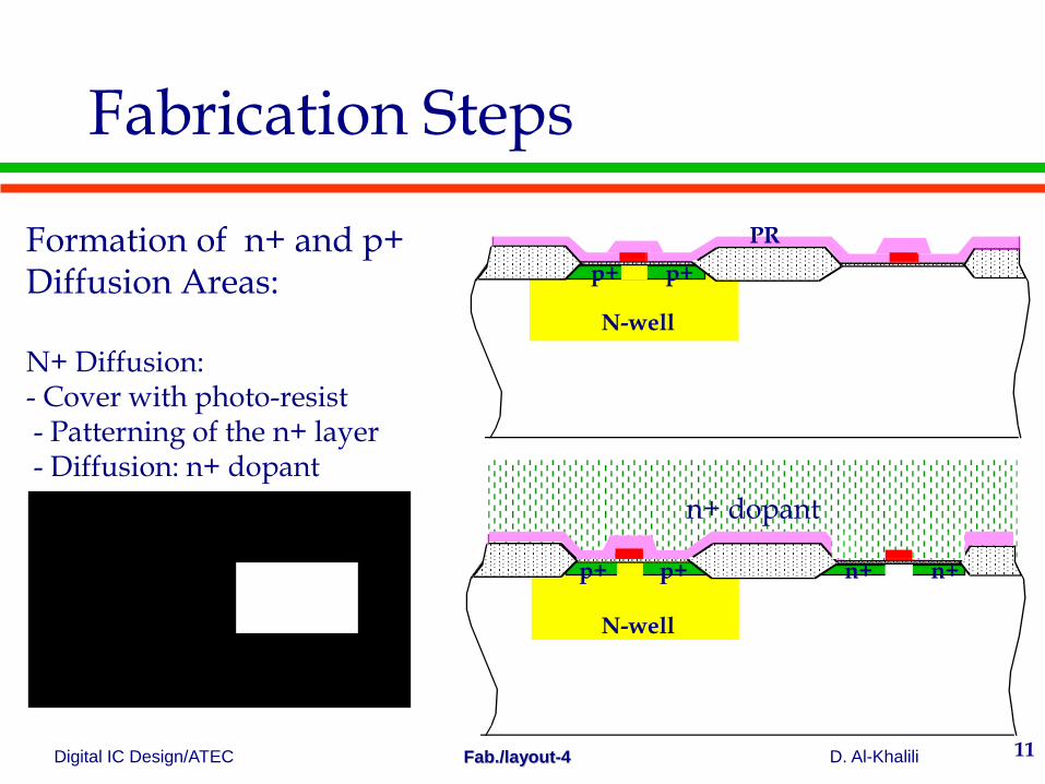
Fabrication Steps
Formation of n+ and p+ Diffusion Areas: N+ Diffusion: - Cover with photo-resist - Patterning of the n+ layer - Diffusion: n+ dopant n+ dopant
PR
N-well
N-well
p+ p+
p+ p+ n+ n+
Digital IC Design/ATEC D. Al-Khalili Fab./layout-4 12
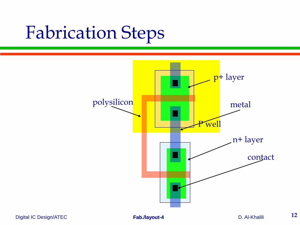
Fabrication Steps
P well
p+ layer
polysilicon
n+ layer
metal
contact
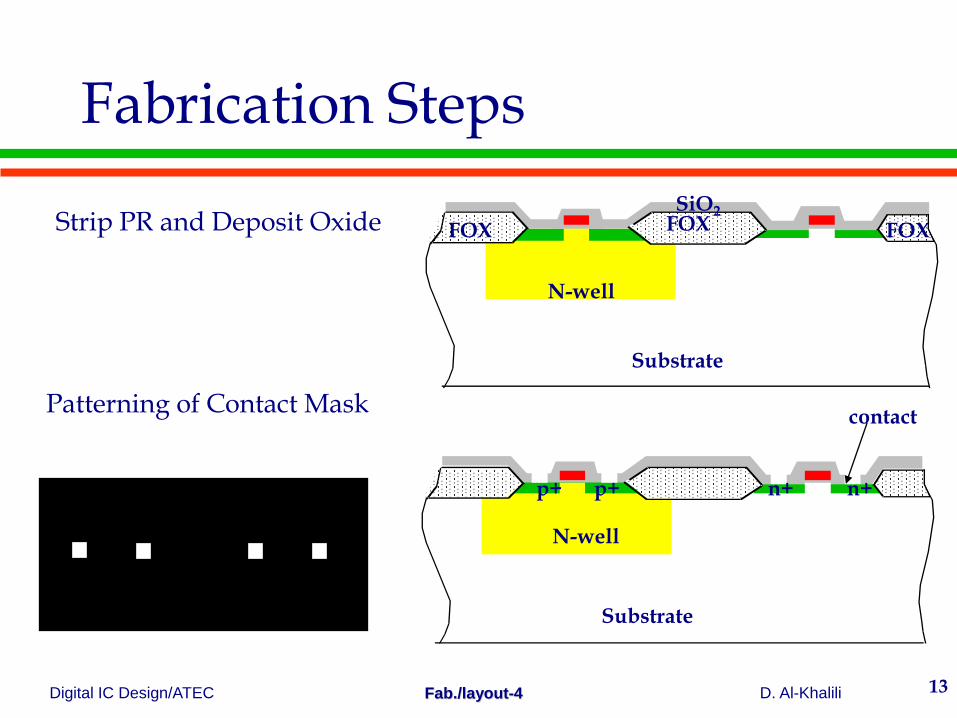
Digital IC Design/ATEC D. Al-Khalili Fab./layout-4 13
Fabrication Steps
Strip PR and Deposit Oxide
Patterning of Contact Mask
SiO2
FOX FOX FOX
N-well
Substrate
p+ p+ n+ n+
N-well
Substrate
contact
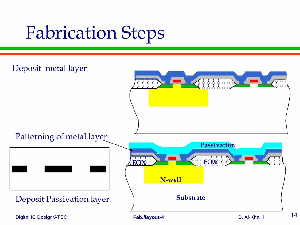
Digital IC Design/ATEC D. Al-Khalili Fab./layout-4 14
Fabrication Steps
Deposit metal layer
Patterning of metal layer
Passivation
N-well
FOX FOX
Substrate Deposit Passivation layer
Digital IC Design/ATEC D. Al-Khalili Fab./layout-4 15
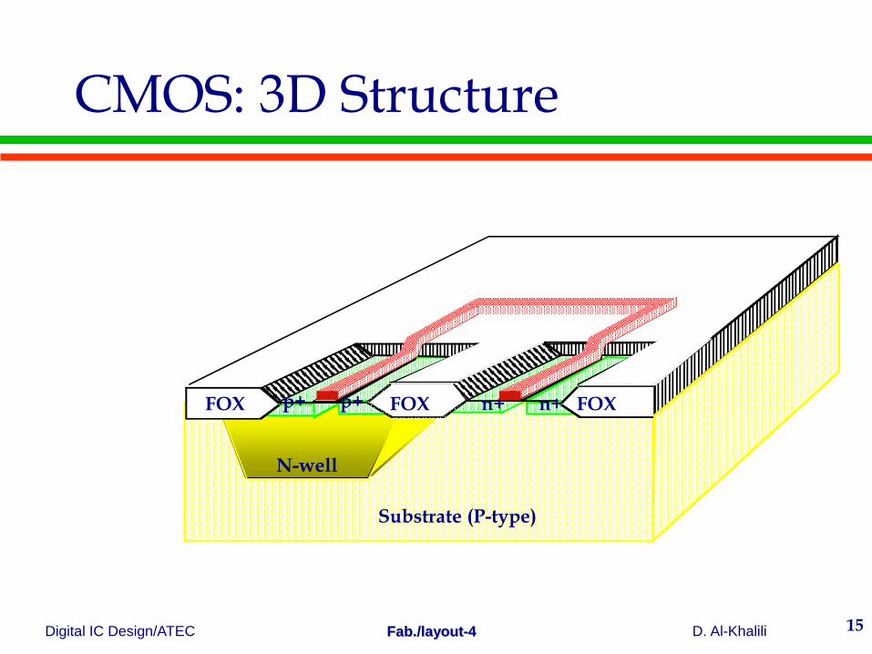
CMOS: 3D Structure
N-well
p+ p+ n+ n+
Substrate (P-type)
FOX FOX FOX
Digital IC Design/ATEC D. Al-Khalili Fab./layout-4 16
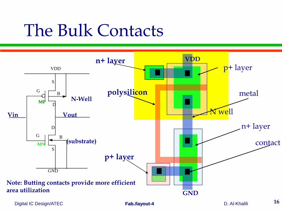
The Bulk Contacts
N well
p+ layer
n+ layer
metal
contact
polysilicon
n+ layer
p+ layer
(substrate)
G
S
D
D
G
S
VDD
GND
B
B
MP
MN
Vin Vout
Note: Butting contacts provide more efficient area utilization
VDD
GND
N-Well
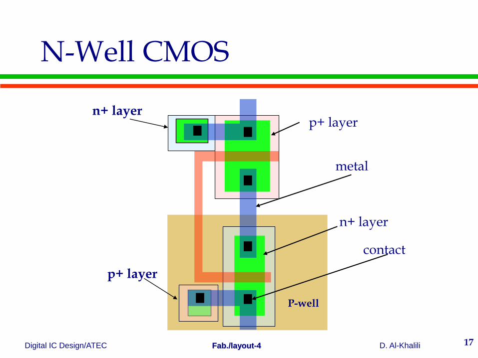
Digital IC Design/ATEC D. Al-Khalili Fab./layout-4 17
N-Well CMOS
p+ layer
n+ layer
metal
contact
n+ layer
p+ layer
P-well
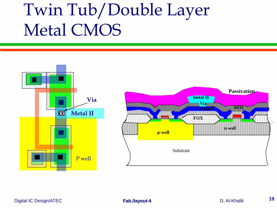
Digital IC Design/ATEC D. Al-Khalili Fab./layout-4 18
Twin Tub/Double Layer Metal CMOS
Substrate
p-well n-wel l
metal II
Passivation
FOX
Via SiO2 Metal I
P well
Metal II
Via
Digital IC Design/ATEC D. Al-Khalili Fab./layout-4 19
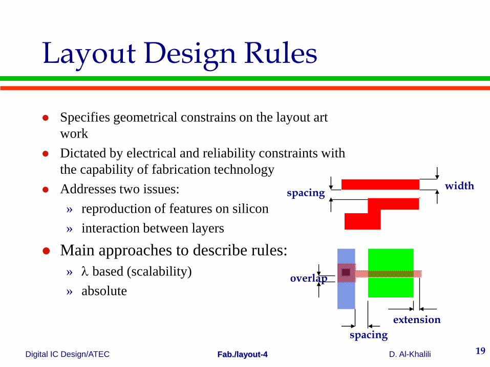
Layout Design Rules
Specifies geometrical constrains on the layout art
work
Dictated by electrical and reliability constraints with
the capability of fabrication technology
Addresses two issues:
» reproduction of features on silicon
» interaction between layers
Main approaches to describe rules:
» based (scalability)
» absolute
width spacing
extension
spacing
overlap
Digital IC Design/ATEC D. Al-Khalili Fab./layout-4 20
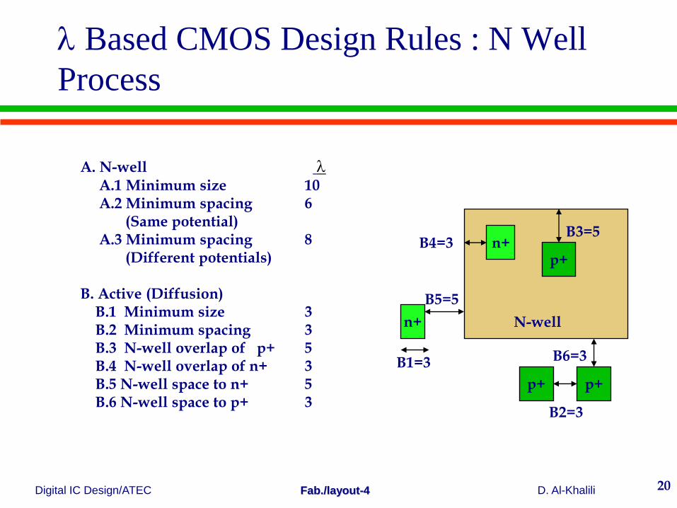
Based CMOS Design Rules : N Well
Process
A. N-well A.1 Minimum size 10 A.2 Minimum spacing 6 (Same potential) A.3 Minimum spacing 8 (Different potentials) B. Active (Diffusion) B.1 Minimum size 3 B.2 Minimum spacing 3 B.3 N-well overlap of p+ 5 B.4 N-well overlap of n+ 3 B.5 N-well space to n+ 5 B.6 N-well space to p+ 3
n+
n+
p+
p+ B4=3
B3=5
B5=5
B6=3
p+
B2=3
B1=3
N-well
Digital IC Design/ATEC D. Al-Khalili Fab./layout-4 21
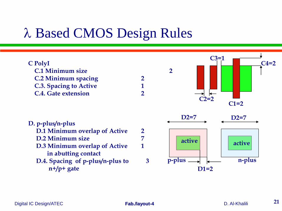
Based CMOS Design Rules
C PolyI C.1 Minimum size 2 C.2 Minimum spacing 2 C.3. Spacing to Active 1 C.4. Gate extension 2 D. p-plus/n-plus D.1 Minimum overlap of Active 2 D.2 Minimum size 7 D.3 Minimum overlap of Active 1 in abutting contact D.4. Spacing of p-plus/n-plus to 3 n+/p+ gate
C2=2 C1=2
C4=2 C3=1
D2=7 D2=7
D1=2
active active
n-plus p-plus
Digital IC Design/ATEC D. Al-Khalili Fab./layout-4 22
Based CMOS Design Rules
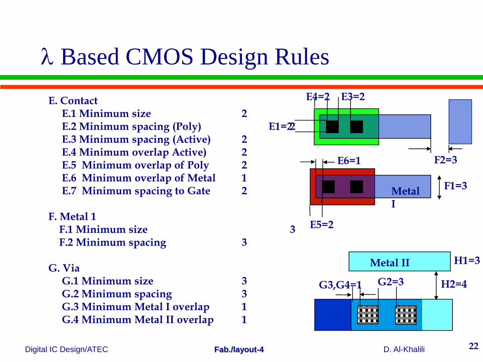
E. Contact E.1 Minimum size 2 E.2 Minimum spacing (Poly) 2 E.3 Minimum spacing (Active) 2 E.4 Minimum overlap Active) 2 E.5 Minimum overlap of Poly 2 E.6 Minimum overlap of Metal 1 E.7 Minimum spacing to Gate 2 F. Metal 1 F.1 Minimum size 3 F.2 Minimum spacing 3 G. Via G.1 Minimum size 3 G.2 Minimum spacing 3 G.3 Minimum Metal I overlap 1 G.4 Minimum Metal II overlap 1
E3=2 E4=2
E1=2
E6=1
E5=2
F1=3
F2=3
H2=4
H1=3
G3,G4=1 G2=3
Metal II
Metal I
Digital IC Design/ATEC D. Al-Khalili Fab./layout-4 23
Based CMOS Design Rules
H. Metal II H.1 Minimum size 3 H.2 Minimum spacing 4 I. Via2 I.1 Minimum size 2 I.2. Minimum spacing 3 J. Metal III J.1 Minimum size 8 J.2. Minimum spacing 5 J.3 Minimum Metal II overlap 2 K. Passivation K.1 Minimum opening 100m K.2 Minimum spacing 150m
Digital IC Design/ATEC D. Al-Khalili Fab./layout-4 24
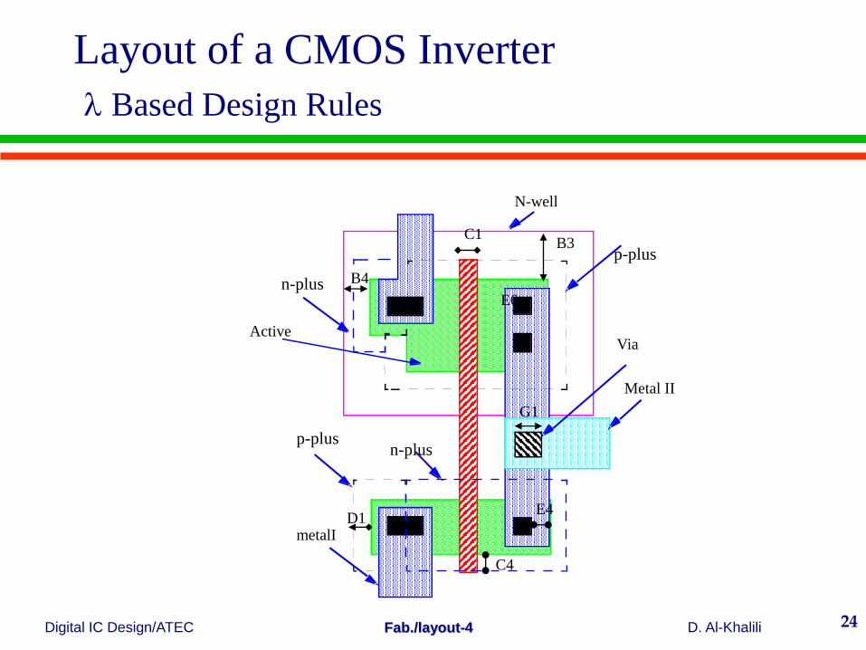
Layout of a CMOS Inverter
Based Design Rules
B3
B4
C1
C4
G1
E4 D1
E6
N-well
n-plus
Metal II
p-plus
metalI
Active Via
p-plus
n-plus
Digital IC Design/ATEC D. Al-Khalili Fab./layout-4 25
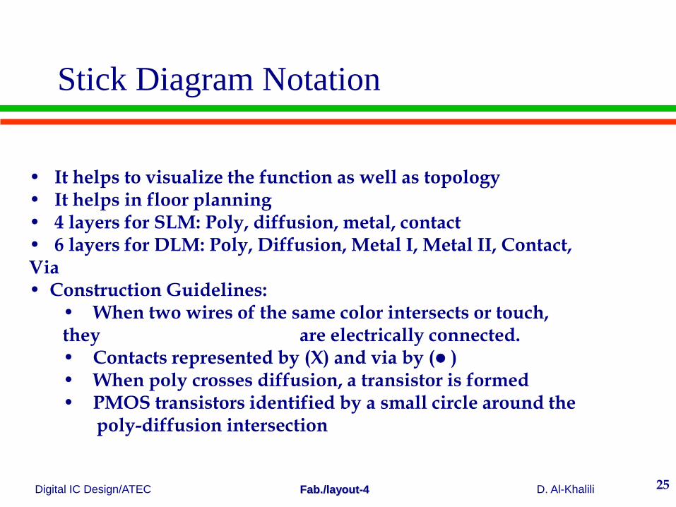
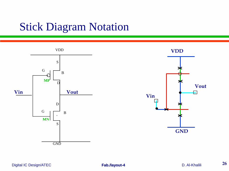
Stick Diagram Notation
• It helps to visualize the function as well as topology • It helps in floor planning • 4 layers for SLM: Poly, diffusion, metal, contact • 6 layers for DLM: Poly, Diffusion, Metal I, Metal II, Contact, Via • Construction Guidelines:
• When two wires of the same color intersects or touch, they are electrically connected. • Contacts represented by (X) and via by ( ) • When poly crosses diffusion, a transistor is formed • PMOS transistors identified by a small circle around the poly-diffusion intersection
Digital IC Design/ATEC D. Al-Khalili Fab./layout-4 26
Stick Diagram Notation
G
S
D
D
G
S
VDD
GND
B
B
MP
MN
Vin Vout Vin
Vout
VDD
GND
Digital IC Design/ATEC D. Al-Khalili Fab./layout-4 27
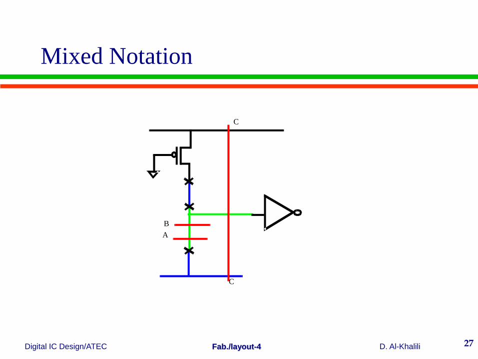
Mixed Notation
A
B
C
C
Digital IC Design/ATEC D. Al-Khalili Fab./layout-4 28
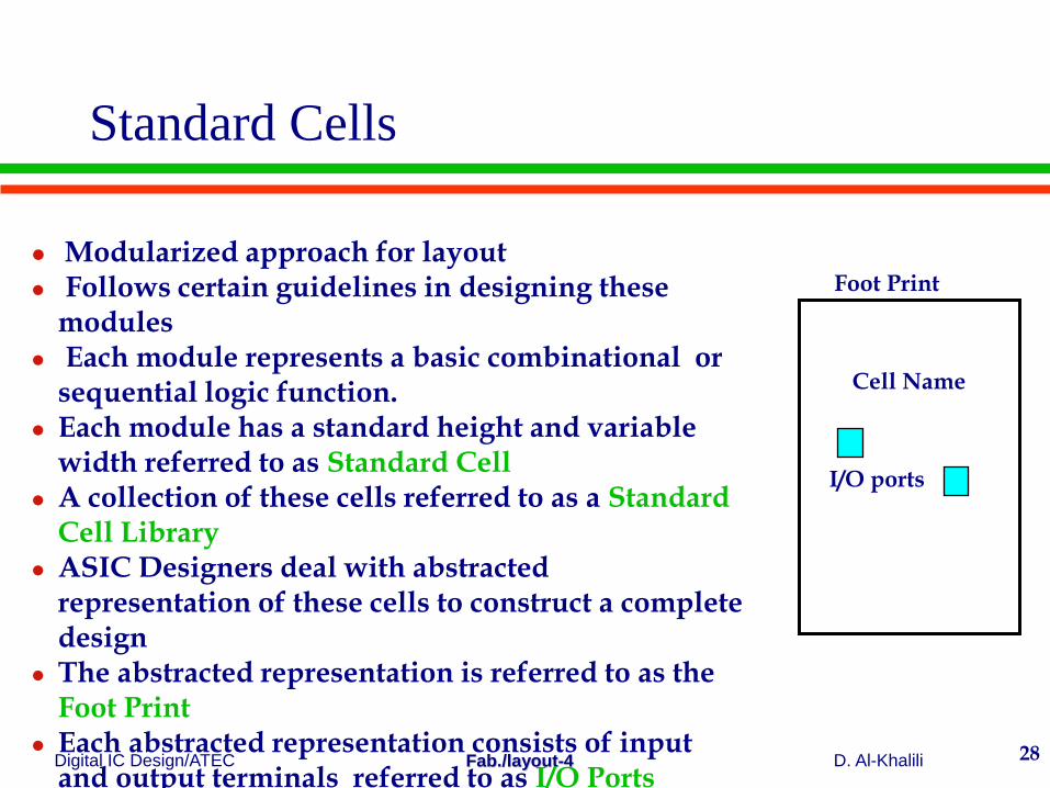
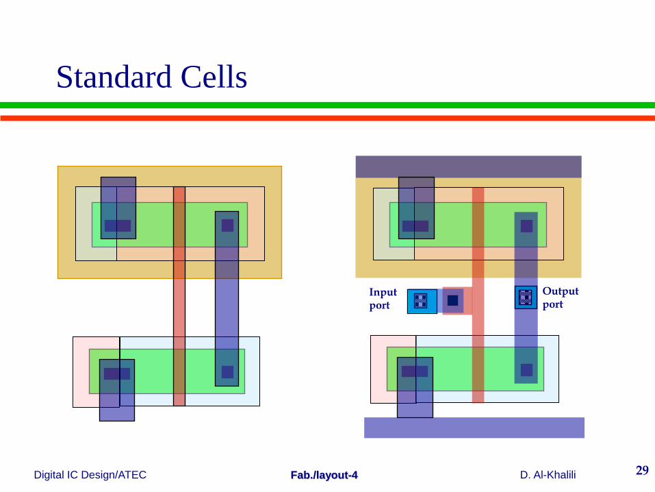
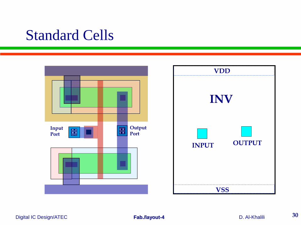
Standard Cells
Modularized approach for layout Follows certain guidelines in designing these
modules Each module represents a basic combinational or
sequential logic function. Each module has a standard height and variable
width referred to as Standard Cell A collection of these cells referred to as a Standard
Cell Library ASIC Designers deal with abstracted
representation of these cells to construct a complete design
The abstracted representation is referred to as the Foot Print
Each abstracted representation consists of input and output terminals referred to as I/O Ports
Cell Name
I/O ports
Foot Print
Digital IC Design/ATEC D. Al-Khalili Fab./layout-4 29
Standard Cells
Input port
Output port
Digital IC Design/ATEC D. Al-Khalili Fab./layout-4 30
Standard Cells
Input Port
Output Port
INV
INPUT OUTPUT
VDD
VSS
Digital IC Design/ATEC D. Al-Khalili Fab./layout-4 31
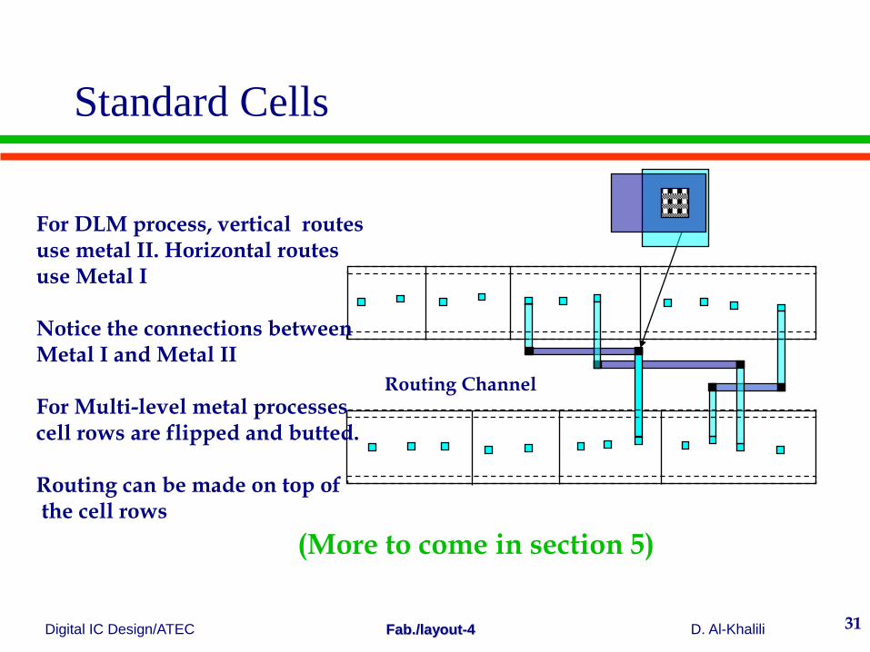
Standard Cells
Routing Channel
For DLM process, vertical routes use metal II. Horizontal routes use Metal I Notice the connections between Metal I and Metal II For Multi-level metal processes cell rows are flipped and butted. Routing can be made on top of the cell rows (More to come in section 5)
Digital IC Design/ATEC D. Al-Khalili Fab./layout-4 32
Yield Analysis
Yield is defined as :
Number of Good chips on wafer X 100% Total Number of chips
Influenced by Defect density Chip area Design rule lithography dimensions Number of mask levels Defects Crystal defects film deposition and growth defects photo-resist imperfections
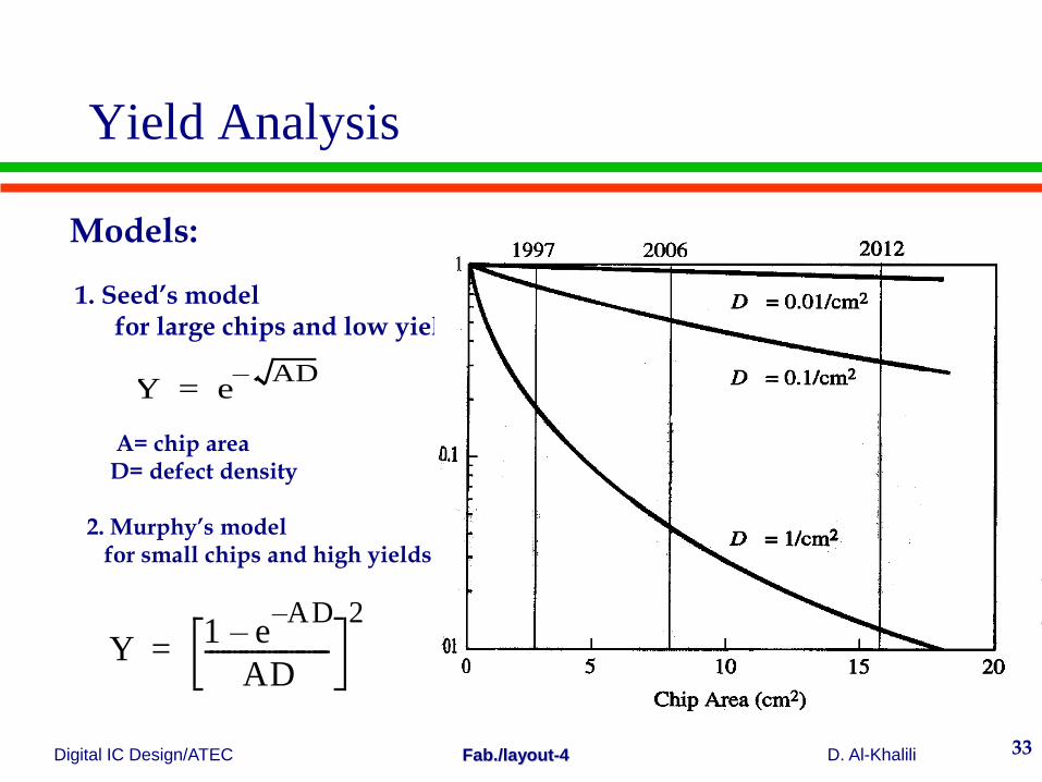
Digital IC Design/ATEC D. Al-Khalili Fab./layout-4 33
Yield Analysis
Y eAD–
=
Y1 e
A– D–
AD----------------------
2
=
Models:
1. Seed’s model for large chips and low yields
A= chip area D= defect density 2. Murphy’s model for small chips and high yields