no.16 november 2009 - eina
TRANSCRIPT

No.16 November 2009
CONTENTS
PREFACE
Research on High Field Electrical Insulation Techniques ························································ 1
OUTLINE OF TECHNICAL COMMITTEES IN IEEJ ······································ 2
Dielectrics and Electrical Insulation (DEI)
Electrical Discharges (ED)
Electrical Wire and Cables (EWC)
Plasma Science and Technology (PST)
Pulsed Electromagnetic Energy (PEE)
Electromagnetic Compatibility (EMC)
Light Application and Visual Science (LAV)
Metal and Ceramics (MC)
Instrumentation and Measurement (IM)
IEC and CIGRE Japanese National Committees Related to Electrical Insulating Materials ··· 16
IEC TC15 Japanese National Committee
IEC TC112 Japanese National Committee
CIGRE SC D1 Japanese National Committee (Materials and Emerging Test Techniques)
RESEARCH ACTIVITIES AND TECHNICAL EXCHANGES
IN ASIAN COUNTRIES
Conference Records ··················································································································· 19
14th Asian Conference on Electrical Discharges (ACED 2008) 19
CIGRE Workshop on Test Techniques and Procedures for HTS Power Applications 21
International Conference on Electrical Engineering (ICEE 2009 Shenyang, China) 23
International Conference on the Properties and Applications of Dielectric Materials
(ICPADM 2009) 26
International Conferences to be held in Asia ················································································ 30
∗ International Conference on Electrical Engineering (ICEE 2010)
∗ International Conference on Condition Monitoring and Diagnosis (CMD 2010)
∗ Asian Conference on Electrical Discharge (ACED 2010)
Activities of Laboratories Laboratory of High Voltage Engineering and Department of Electrical Power Engineering
at Hasanuddin University ··········································································································· 32
China Corner ································································································································ 35
The 354th XSSC on nano-dielectrics
2009 Lecture Series for Graduate Students (LSGS 2009) in Xi’an
Korea Corner ································································································································· 38
High Power High Voltage Testing & Evaluation Division at KERI
India Corner ··································································································································· 40
Central Power Research Institute, India – a Brief Profile
TECHNOLOGIES FOR TOMORROW
Development of large-capacity, 3-phase, 500kV transformer that is disassembled

for shipment and reassembled at the site ························································································· 43
The Largest Scale Dielectric Tests of 1100kV Gas Circuit Breaker ············································· 46
TECHNOLOGIES ALERT
Electrostatic Potential Distribution Measurement in Vacuum ························································ 48
MISCELLANEOUS
Photos on Front and Rear Covers······································································································ 49
Transactions of IEEJ ························································································································· 50
IEEJ Technical Reports ················································································································· 51
Application for Membership of IEEJ ······························································································ 52
Way for Purchasing Proceedings of IEEJ Technical Meetings and IEEJ Technical Reports ········· 52
Members of EINA Committee in 2009 ····························································································· 54
Web Site for EINA Magazine ······································································································· 54
EINA No.16 (November 2009) 1
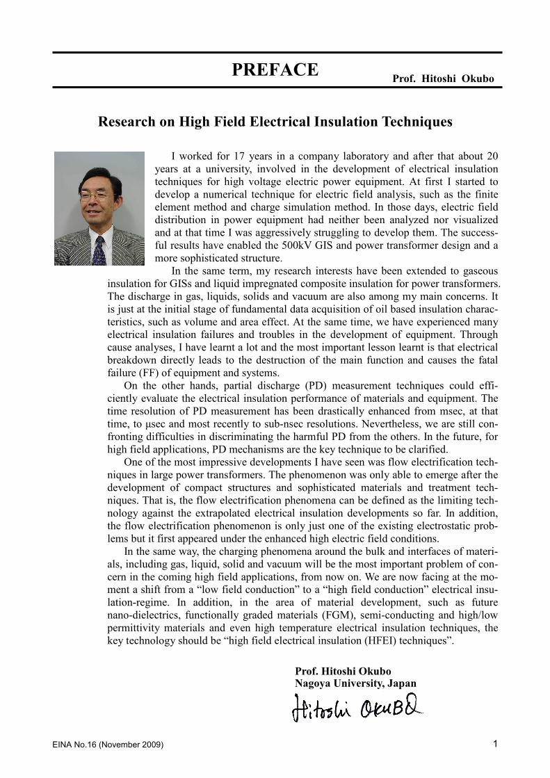
PREFACE
Research on High Field Electrical Insulation Techniques
I worked for 17 years in a company laboratory and after that about 20
years at a university, involved in the development of electrical insulation
techniques for high voltage electric power equipment. At first I started to
develop a numerical technique for electric field analysis, such as the finite
element method and charge simulation method. In those days, electric field
distribution in power equipment had neither been analyzed nor visualized
and at that time I was aggressively struggling to develop them. The success-
ful results have enabled the 500kV GIS and power transformer design and a
more sophisticated structure.
In the same term, my research interests have been extended to gaseous
insulation for GISs and liquid impregnated composite insulation for power transformers.
The discharge in gas, liquids, solids and vacuum are also among my main concerns. It
is just at the initial stage of fundamental data acquisition of oil based insulation charac-
teristics, such as volume and area effect. At the same time, we have experienced many
electrical insulation failures and troubles in the development of equipment. Through
cause analyses, I have learnt a lot and the most important lesson learnt is that electrical
breakdown directly leads to the destruction of the main function and causes the fatal
failure (FF) of equipment and systems.
On the other hands, partial discharge (PD) measurement techniques could effi-
ciently evaluate the electrical insulation performance of materials and equipment. The
time resolution of PD measurement has been drastically enhanced from msec, at that
time, to µsec and most recently to sub-nsec resolutions. Nevertheless, we are still con-
fronting difficulties in discriminating the harmful PD from the others. In the future, for
high field applications, PD mechanisms are the key technique to be clarified.
One of the most impressive developments I have seen was flow electrification tech-
niques in large power transformers. The phenomenon was only able to emerge after the
development of compact structures and sophisticated materials and treatment tech-
niques. That is, the flow electrification phenomena can be defined as the limiting tech-
nology against the extrapolated electrical insulation developments so far. In addition,
the flow electrification phenomenon is only just one of the existing electrostatic prob-
lems but it first appeared under the enhanced high electric field conditions.
In the same way, the charging phenomena around the bulk and interfaces of materi-
als, including gas, liquid, solid and vacuum will be the most important problem of con-
cern in the coming high field applications, from now on. We are now facing at the mo-
ment a shift from a “low field conduction” to a “high field conduction” electrical insu-
lation-regime. In addition, in the area of material development, such as future
nano-dielectrics, functionally graded materials (FGM), semi-conducting and high/low
permittivity materials and even high temperature electrical insulation techniques, the
key technology should be “high field electrical insulation (HFEI) techniques”.
Prof. Hitoshi Okubo Nagoya University, Japan
Prof. Hitoshi Okubo
EINA No.16 (November 2009) 2
OUTLINE OF TECHNICAL COMMITTEES IN IEEJ
Dielectrics and Electrical Insulation (DEI)
Chairperson: Naohiro Hozumi (Aichi Institute of Technology)
Secretaries: Yasuhiro Tanaka (Tokyo City University)
Yuichi Ashibe (Sumitomo Electric Co. Ltd.)
Assistant Secretaries: Toshihiro Takahashi (CRIEPI)
Takahiro Imai (Toshiba Co. Ltd.) Annual Symposium of Electrical and Electronic
Insulating Materials and Applications in Systems
(SEEMAS) and International Symposium on
Electrical Insulating Materials (ISEIM) are
important activities of TC-DEI. This year we held
the SEEMAS, the domestic, in Matsue city, hosted
by colleagues of Matsue National College of
Technology. As well as the success of the ISEIM
last year, this year's symposium was quite
sensational.
Fig. 1 indicates that this domestic symposium
used to be growing in its scale until the year of
1990. It is remarkable that the symposium
maintained its scale even after our "bubble
economy" collapsed. The symposium, however,
turned into shrinkage after the year of 2000,
correlating to the structural change in our economy.
In 2006, the TC-DEI member started to
reorganize the symposium. We aimed to promote
the linkage between academia and industry, and
encouraged the activity of young researchers. It is
amazing that the number of participants has been
increasing gradually since that time, and finally this
year it has recovered to be the same level as the
most active time. It is also quite impressive that,
although the symposium was domestic, we had ten
participants from Korea this year. We recognize that
collaboration with Asian researchers is one of hot
issues these days.
Nano-composite materials, insulation systems
under inverter surges, space charge assessment,
asset management regarding to insulation
performance, outdoor insulations, thin dielectric
films and other topics were discussed. After the
symposium, we had the young researcher's seminar.
We will hold the domestic symposium again in
2010. The international symposium (ISEIM) will be
held in the autumn of 2010 in Kyoto or vicinity, in
cooperation with CIGRE SC-D1 colloquium. We
are expecting your participation.
0
20
40
60
80
100
120
140
160
180
1965 1970 1975 1980 1985 1990 1995 2000 2005 2010
Year
Number
participants
presentations
(banquet)
0
20
40
60
80
100
120
140
160
180
1965 1970 1975 1980 1985 1990 1995 2000 2005 2010
Year
Number
participants
presentations
(banquet)
Fig. 1. Transition of attendants at the symposium.
The expected transition after 2009 may be too
extreme and not suitable to maintain the sense of
affinity among attendants.
Fig. 2. The venue of this year's SEEMAS was
idealistic that all participants spent three days in the
same hall, in which both oral and poster sessions
were held. We could freely visit poster booth during
the intermissions of oral session.
Furthermore, the TC-DEI runs Investigation
Committees (IC's) that organize several technical
meetings a year. The investigation committees are
categorized into four research areas:
Macro-view of DEI technology related
> Asset Management for Electric Power Equipments
Based on Insulation Diagnosis (04/2008-03/2011,
Chairperson: M. Ikeda (Nippon Petroleum Refining Co.)).

EINA No.16 (November 2009) 3
New materials including nano-materials related
> Nano-Interface Properties of Organic and
Composite Thin Films and Device/Sensor
Applications (10/2007 - 09/2010, Chairperson: K.
Kato (Niigata University)).
> Physics of Organic Dielectrics/Semiconductors
and Interfacial Design (04/2007 - 03/2010,
Chairperson: M. Iwamoto (Tokyo Institute of
Technology))
> Polymer Nanocomposites and their Applications
as Dielectrics and Electrical Insulation (01/2006 -
12/2008, Chairperson: T. Tanaka (Waseda
University)). Next activity is being planned.
Ageing and diagnosis of electric and electronic
equipment related
> Degradation Diagnosis Technology based on Characteristics of Insulation Materials in Electric
Power Apparatus (04/2007 - 03/2010, Chairperson:
Y. Ehara (Tokyo City University)).
> Partial Discharge Measurement Under Repetitive
Impulse Voltage Application (08/2007 - 07/2010,
Chairperson: M. Hikita (Kyushu Institute of
Technology)). The committee is cosponsored by
the TC-DEI and TC of Electrical Discharge.
Basic dielectric and breakdown phenomena
related
> Standardization of Calibration and Development of Application on Space Charge Measurement using PEA
Method (03/2009-02/2012, Chairperson: Y. Tanaka
(Tokyo City University)).
> Surface Properties and Long-term Performance of
Polymeric Insulating Materials for Outdoor Use
(01/2006 - 12/2008, Chairperson: H. Homma
(CRIEPI)). Technical report will be issued soon.
Electrical Discharges (ED)
Chairperson: Masayuki Hikita (Kyushu Institute of Technology)
Vice-chairperson: Toshiki Nakano (National Defense Academy)
Secretaries: Fumiyoshi Tochikubo (Tokyo Metropolitan University)
Akiko Kumada (University of Tokyo)
Assistant Secretaries: Yasushi Yamano (Saitama University)
Mina Sakano (Toshiba Corporation)
The Technical Committee on Electrical
Discharge (TC-ED) belongs to the Fundamentals
and Materials Society (A-Society) of the IEE Japan.
The purposes of the TC-ED are mainly in the wide
promotion of the research activities concerning to a
variety of electrical discharges in vacuum, gas,
liquid and on surfaces of materials and their
applications to high technologies..
Several investigation committees, which are the
affiliates of the TC-ED, are established every year
to survey the up-to-date research subjects. The
activities of these committees usually continue for
three years. The chairpersons shown in Table 1
currently run five investigation committees. In
addition, the investigation committee for the
modeling of lightening strokes to structures is
planned and will be established this year.
The TC-ED organizes about six domestic
technical meetings on electrical discharges every
year. In these meetings, about 200 full papers are
presented in total from both academic and industrial
sides by researchers, engineers, professors and
students. The domestic technical meetings are
sometimes co-organized by other Technical
Committees on such as High Voltage Engineering,
Pulse Electromagnetic Energy, Plasma, and
Dielectric /Electrical Insulating Materials.
In order to promote the international activities in
electrical discharges, “Japan-Korea Joint
Symposium on Electrical Discharge and High
Voltage Engineering” has been organized by the
TC-EC and has been held every two years. The next
J-K Symposium is held on the November 5-7 of
2009 in Busan, Korea. The special issue of this
symposium will be published in the IEEJ
Transactions on Fundamentals and Materials IEE
Japan in October of 2010.
The TC-ED also contributes to the organization
of a young researcher seminar every year in
cooperation with the Institute of Engineers on
Electrical Discharges in Japan to encourage the
young researchers in the field of electrical
discharges. About 40 young researchers and
engineers participate in the seminar and discuss
vigorously the topics related to electrical discharges
for two days.

EINA No.16 (November 2009) 4
Electrical Wire and Cables (EWC)
Chairperson: Yasuo Suzuoki ( Nagoya University )
Secretary: Kazushi Nakaya ( EXSYM Corporation )
Assistant Secretary: Akitoshi Watanabe ( VISCAS Corporation )
Hitoshi Nojo (J-Power Systems Corporation)
Technical Committee on Electrical Wire and
Cables (TC-EWC) is a committee organized to
support the IEEJ Power and Energy Society, and
comprises members from universities, power
utilities, the JR railway company, Japan Electric
Cable Technology Center(JECTEC)and cable
manufacturers. The technical committee organizes
technical meetings to promote R&D activities in
this field and provides an opportunity to present
technical achievements. Three technical meetings
were so far held in 2009. A technical meeting on
deterioration diagnosis and online monitoring
system was held as a joint meeting with TC-DEI on
February 19 in Tokyo. A symposium on technical
trends in measures for age deterioration of electric
wires and cables was held on March 19 in Sapporo,
Hokkaido. A discussion meeting on
environment-friendly technologies for resins was
held on August 18 in Tokyo. The technical
committee plans to organize 4 more meetings in
FY2009.
In addition to organizing such technical
meetings, the technical committee supervises
investigation committee dealing with subjects
relating to electrical wire and cables. During the last
several years, Investigation Committee for
Technology of Wires and Associated Accessories
for Overhead Transmission Lines, Investigation
Committee for Accessories for 66kV and Higher
Voltage XLPE Power Cable, and Investigation
Committee for Technology of XLPE Power Cable
and Associated Accessories for Underground
Distribution were organized. This year, two
investigation committees are in action as listed in
Table 1.
Table 1 Investigation Committee in TC-EWC
Research Subject Chairperson
Technical Trend of Environmental
Tests for Insulation Materials of
Distribution Wires and Cables
S. Nishimura
Recent Technological Trends in
Overseas Power Transmission Cables M. Hikita
Discussion Meeting on environment-friendly
technologies for resins (August 18, 2009, Tokyo)
Table 1 Investigation Committees in TE-ED
Chairperson Research subjects and established time
S. Matsumoto
(Shibaura Institute of Technology)
Present situation of lightening discharge simulation technologies
and comparison of the simulation models (established in
December 2006)
M. Hikita
(Kyushu Institute of Technology)
Measurement of the partial discharges generated by repetitive
impulse voltage (established in August 2007)
E. Hotta
(Tokyo Institute of Technology)
Generation control and applications of vacuum and low-pressure
discharges (established in October 2007)
R. Hanaoka
(Kanazawa Institute of Technology)
Discharge phenomena in liquid dielectrics and the technologies of
EHD,ER and MR applications (established in December 2007)
M. Amakawa
(Central Research Institute of
Electric Power Industry)
Technologies of arc and glow discharge applications
(established in May 2008)
EINA No.16 (November 2009) 5
Plasma Science and Technology (PST)
Chairperson: Ken Yukimura (Doshisha University)
Scientific Secretary: Kungen Teii (Kyushu University)
Scientific Secretary Assistance: Hiroshi Akatsuka (Tokyo Institute of Technology)
The Technical Committee on Plasma Science
and Technology (TC-PST) was founded in April
1999. This committee has the basis on the plasma
researcher’s society that had organized Technical
meeting on plasma science and technology in IEE
Japan several times every year since about 30 years
ago. The field of activity of this committee includes
researches and investigations of various plasmas in
terms of plasma physical parameters as density,
temperature and ionization degree, and application
fields as nuclear fusion, plasma processing, and
plasma chemistry.
The major activity of this committee is to
succeed to organize several technical meeting on
plasma science and technology every year. In 2009,
four technical meeting were held; in June at Saga
University in Saga, in August at Doshisha
University in Kyoto, in September at Osaka
Prefecture University in Osaka, in November at
Tokyo City University in Tokyo. In 2008, five
technical meetings were held. At each symposium,
about 20 or 30 presentations are made.
Presentations by young researchers in bachelor
course and master course are strongly encouraged
and appreciated.
Every two years, TC-PST sponsored
international symposium APSPT (Asia-Pacific
International Symposium on the Basics and
Applications of Plasma Technology) had been held
in Taiwan in collaboration with Japanese domestic
societies related to plasma science and technology
since 1999. Recently, APSPT-5 was held in
Kaohsiung in Taiwan in December, 2007. Aiming
at more flexible management, APSPT became
sponsorship by the international organization
committee from APSPT-4. While many members of
TC-PST participate in the international organization
committee, TC-PST continues playing a role
important as a support organization.
APSPT-6 (http://apspt6.must.edu.tw) will be
held at Mingshin University of Science and
Technology, Hsinchu, Taiwan, R.O.C. in December
14-16, 2009. Several invited lectures and over 120
contribution papers are going to be presented in this
symposium.
TC-PST currently runs two investigation
committees as shown in Table 1. Here we introduce
their activities. In the committee of the
plasma–water applications and their reacting
processes involved in liquid interfaces, various
types of discharge-plasma applications have been
systematically investigated by the experts in this
field to deepen the understanding of plasma–water
interacting phenomena at liquid surface boundaries.
This comprehensive research covers the
decomposition of persistent organics, the
microorganism disinfection and the material
synthesis. In the committee of the kinetic
description of low-temperature plasmas with
applications to modeling and simulation, with the
widespread use of low-temperature plasmas in the
field of energy conversion and environmental
control, development of numerical models
incorporating physical and chemical phenomena
play a key role. The goal of this committee is to
provide recent advances in plasma kinetic theory
and its potential impact on their work. In 2009,
authoritative researchers will summarize how they
use plasma simulations.
The investigating committees dispersed recently,
the plasma ion intensive use process investigation
committee, the microwave plasma investigation
committee, and the advancement of metal
sputtering plasma committee had published their
investigation as hard cover books, and it was useful
for these books to systematize the newest
technology trends of these fields.
(presented by Kungen Teii, Kyushu University)
Table 1. Investigation Committee in TC-PST
Plasma–Water Applications and their Reacting
Processes Involved in Liquid Interfaces
3 years from 2008, Chairperson: K. Yasuoka
(Tokyo Institute of Technology)
Kinetic Description of Low-Temperature Plasmas
with Applications to Modeling and Simulation
3 years from 2008, Chairperson: S. Kambara
(Gifu University)
EINA No.16 (November 2009) 6
Pulsed Electromagnetic Energy (PEE)
Chairperson: Eiki Hotta (Tokyo Institute of Technology)
Vice Chairperson: Koichi Takaki (Iwate University)
Scientific Secretary: Sunao Katsuki (Kumamoto University)
Scientific Secretary Assistance: Shinji Ibuka (Tokyo Institute of Technology) Pulsed electromagnetic energy produced by pulsed
power, which refers to huge power within an extremely
short period of time. The power level reaches 300 TW in
the world largest pulsed power machine, Z accelerator in
Sandia National Laboratory, USA. The period of time
goes down to sub-nanosecond range. Pulsed power is
often focused in a narrow space to produce an extremely
high power density. Pulsed power is basically produced by means of a rapid energy transfer from an energy
storage medium to the load. The pulse power technology
and the pulsed electromagnetic energy have greatly
expanded their regimes in technological and application
fields, based on the state-of-the-art technology of power
devices. Trend of the device is shifted from a single-shot
huge machine to highly repetitive compact devices.
The research field of the Technical Committee on
Pulsed Electromagnetic Energy covers the electric power
engineering, plasma and discharge engineering, high
energy density physics, accelerator engineering,
bio-medical engineering and also pulse power device
itself. By the modification of pulsed electromagnetic
energy, we can make an extremely high energy density
(high temperature and/or high density) state with well
defined condition, which can be utilized for generations
of high power lasers, intense radiation sources, high
current particle beams and also for formation of new
materials. The pulsed power technology is also capable
of efficiently producing non-thermal equilibrium plasmas.
A large volume, atmospheric pressure non-thermal
plasmas is utilized for decomposition of toxic gases,
ozone synthesis and sterilization. The pulsed power
driven underwater discharge plasmas can be utilized for
cleaning the water environment. The pulsed power
discharges in composite matter are used for the recycling
of aggregate in concrete blocks and of electronic parts in
circuit board.
Recently, application of pulsed power to biological
targets and its applications, which are called
“bioelectrics”, has been glowing since 2000, in USA,
Europe and Japan. The Investigation Committee on
“Biological Effects of Pulsed Electromagnetic Energy
and Their Innovative Applications” was established in
January 2009. Since bioelectrics has a multi-disciplinary
nature, this committee provides a forum to discuss
important technical developments, their applications,
increased understandings, new trends, and also future
prospects in the interdisciplinary field. It is predicted that
new knowledge should open an innovative application in
wider field such as biotechnology, medical engineering,
environmental engineering, agriculture and food
processing. Here we introduce a couple of topics in the
field of pulsed electromagnetic energy and pulsed power
technology.
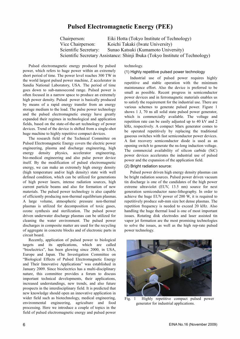
(1) Highly repetitive pulsed power technology
Industrial use of pulsed power requires highly
repetitive and stable operation with the minimum
maintenance effort. Also the device is preferred to be
small as possible. Recent progress in semiconductor
power devices and in ferromagnetic materials enables us
to satisfy the requirement for the industrial use. There are
various schemes to generate pulsed power. Figure 1
shows 1 J, 70 ns all solid state pulsed power generator,
which is commercially available. The voltage and
repetition rate can be easily adjusted up to 40 kV and 2
kHz, respectively. A compact Marx generator comes to
be operated repetitively by replacing the traditional
gaseous switches with fast semiconductor power devices.
A fast recovery semiconductor diode is used as an
opening switch to generate the ns-long induction voltage.
The commercial availability of silicon carbide (SiC)
power devices accelerates the industrial use of pulsed
power and the expansion of the application field.
(2) Bright radiation source:
Pulsed power driven high energy density plasmas can
be bright radiation sources. Pulsed power driven vacuum
tin discharge is one of the candidates of the high power
extreme ultraviolet (EUV, 13.5 nm) source for next
generation semiconductor nano-lithography. In order to
achieve the huge EUV power of 200 W, it is required to
repetitively produce sub-mm size hot dense plasmas. The
repetition frequency is needed to exceed 20 kHz. Also
handling the huge thermal load is one of most important
issues. Rotating disk electrodes and laser assisted tin
vapor jet formation are the most promising technologies
to solve the issues, as well as the high rep-rate pulsed
power technology.
Fig. 1 Highly repetitive compact pulsed power
generator for industrial applications.

EINA No.16 (November 2009) 7
(3) Gas treatment:
The sub-10 ns pulsed power is capable of efficiently
producing non-thermal large volume plasmas in
atmospheric pressure gases since only electrons are given
a high energy from the field in the period of time. A large
number of high energy electrons collide with neutrals to
produce chemically active species such as radicals, ions,
excited state molecules. These active species react with
harmful components for human health or environment,
as the result, the harmful components is decomposed and
changes to harmless components. The pulsed power
discharge plasmas in the atmospheric gas pressure are
used for NOx (nitrogen oxide) removal from combustion
exhaust gas, VOC (Volatile organic compound)
decomposition and ozone synthesis in addition to the
sterilization of medical appliances, surgical instruments
and foods.
(4) Food processing:
Low temperature sterilization of liquid using intense
pulsed electric fields (PEF) has been studied in the past
tens of years to preserve ingredients of nutrition.
However, the PEF sterilization is implemented in the
limited cases since the PEF shows less effect on bacterial
spores. Recent progress in pulsed power technology
enables us to kill spores. Figure 2 shows the result of
PEF sterilization of bacillus subtilis spores both by the
100 kV/cm PEF treatment and by the conventional heat
sterilization. The contaminated liquid flows continuously
between two parallel electrodes in a treatment vessel.
Degree of sterilization, defined as log(N0/N), depends on
the treatment temperature both in the PEF and in the heat
treatments, where N0 and N are the initial and the
surviving bacteria numbers, respectively. The bacterial
spores are inactivated only for the temperature exceeding
100℃. The use of PEF lowers the treatment temperature
by approximately 10℃, which help preserve ingredients
of nutrition and flavor. Also the intense PEF is used to
extract efficiently juice from plants. Cell membrane of
target plant becomes permeable by applying PEF. This
technology has been implemented and applied to sugar
beats and grapes.
(5) Biological applications:
Non-thermal intense nanosecond pulsed electric
fields (nsPEF) or narrowband burst radio frequency
fields seemingly gives a unique stress to intracellular
organelles and/or bio-molecules. Applying nsPEF is
capable of inducing apoptosis to cancer cells, which will
potentially be used for cancer therapy. Figures 3(a) and
(b) show microscopic snapshots of intact HeLa cells and
those exposed to an intense burst sinusoidal electric field
(IBSEF, 2 kV/cm, 100 MHz, 1 ms). The pulsed cells are
obviously inactivated. The time for doubling the number
for the cells exposed to the field is approximately 35
hours, which is approximately 2 times as long as that of
the sham control. Other bio-chemical analysis using
fluorescent molecular probes indicates a portion of the
cells went dead via the process of apoptosis. Also ns PEF
is capable of activating platelet, which can be applied for
wound healing. Similarly the nsPEF induced biological
stresses or stimuli will potentially be used for
agricultural applications, such as seed germination,
growth control.
Fig. 2 Comparison between pulsed electric field
and thermal sterilizations of bacillus subtilis
spore in liquid as functions of their treatment
temperature. The picture is a transmission
electron microscope (TEM) image of spore.
(a) Sham control
(b) HeLa cells exposed to 100 MHz IBSEF
Fig. 3 Microscopic snapshot of cancer cells (HeLa
cells) exposed to 2 kV/cm 100 MHz IBSEF,
cultured for 36 hours on the slide.

EINA No.16 (November 2009) 8
Electromagnetic Compatibility (EMC)
Chairperson: Tsuyoshi Funaki (Osaka University)
Secretaries: Ken Kawamata (Hachinohe Institute of Technology),
Tomoo Ushio (Osaka University)
Yoshinori Taka (Nagoya Institute of Technology) The Technical Committee on Electro-Magnetic
Compatibility (EMC) has a vital role of researching
following subjects;
1. Comprehensive understanding of electrical
power system and EMC issue,
2. Building up interdisciplinary cooperation
among several groups and/or institutes related
with EMC problem,
3. Investigations on new and high technology for
EMC,
4. Advertisement to the public on EMC issue and
key technologies,
5. Introductory advertisement of international
EMC standard to the domestic EMC
researchers.
For these purposes the committee pays their
attention to the causes of electromagnetic
interference, the situation of electromagnetic
interferences, the novel measurement techniques for
EMC, the protection technology for EMC and
international and domestic EMC regulations. The
committee has been organizing four dedicated
research sub-committees to realize the effective
activity.
1. Investigation committee on security
technology for electromagnetic wave and
information.
2. Investigation committee on evaluation
technologies for induced electric field and
current in a human body caused by
non-uniform and transitional electromagnetic
fields.
3. Investigation committee on noise immunity
for electric and electrical appliances.
4. Investigation committee on EMC
technologies for electrostatic discharge (ESD).
These sub-committees basically work independently,
and each sub-committee meeting is held every two
or three months regularly to announce their
investigations and to share the obtained knowledge
among sub-committee members. The practical
period for the sub-committee activity is two or three
years, and they are expected to publish their
investigating results as a technical report of
investigation committee.
Electromagnetic environment is the field, where
electromagnetic phenomena exist. They are
electromagnetic fields due to naturally-originated
sources like lightning and earthquake, and artificial
ones generated from electrical and electronic
equipment as well as radiated from power lines or
communication cables, and so force. EMC is the
capability of electrical and electronic systems,
equipment and devices to operate in the
above-mentioned electromagnetic environment,
without suffering or causing unacceptable
degradation as a result of electromagnetic
interference. In other words, a system is considered
as electromagnetically compatible if it satisfies the
following three criteria:
(1) It does not cause interference with other
systems;
(2) It is not susceptible to emissions from other
systems;
(3) It does not cause interference with itself.
The problems related to EMC had been
discussed in the “Special Research Committee of
EMC Engineering”, which was established in 1997
by IEICE and IEEJ joint venture. The high activity
of the committee promoted the establishment of the
technical committee on EMC in the Fundamentals
and Materials Society of IEEJ. The committee was
established to substitute the former committee in
April 1999. Then Prof. T. Takuma of Kyoto
University was elected as the first chair of the
committee. After that, Prof. O. Fujiwara and Prof.
Z-I. Kawasaki chaired the committee respectively
from 2002 to Apr. 2005, and from May 2005 to Apr.
2008. Currently, Prof. T. Funaki succeeds the chair
since May. 2008.
The committee holds some technical
conferences. They were June 5th, Nov. 13
th, Dec.
19th for 2008, and Jan. 21th, Mar. 6
th for 2009. This
year, the committee technically co-sponsored the
2009, international symposium on electromagnetic
compatibility, Kyoto, which was held Jul. 20th-24
th,
2009.
1. Investigation Committee on Security Technology

EINA No.16 (November 2009) 9
for Electromagnetic Wave and Information
This committee has started its activity in April
2007. Dr. Shinji Seto of NICT is chairing this
committee. The Objectives of the committee
activity are followings
1. Surveying the security technology for
electromagnetic wave and information,
including needs, terminology, and standards,
2. Surveying the eavesdrop by TEMPEST like
technology, including current status,
documents, threat, and counter measurement,
3. Surveying the attacking by Intentional-EMI,
including current status, documents, threat, and
counter measurements.
The committee is focusing on establishing secure
and safety world with preparing the adequate (not
exceed) countermeasure for the prospective
electromagnetic threats.
2. Investigation Committee on Evaluation
Technologies for Induced Electric Field and
Current in a Human Body Caused by
Non-uniform / transient Electromagnetic Fields
This committee was established in July 2006 for
taking over from the previous Investigation
Committee on Electric Field and Current Induced in
a Human Body Exposed to Electromagnetic Fields.
The mission of the committee is to investigate the
methods for calculating the induced electric field
and current in a body caused by non-uniform and/or
transient electromagnetic fields, and survey articles
regarding the related calculation results. This
committee also investigates measurement methods,
which is indispensable in modeling electromagnetic
field source to simulate practical exposure
conditions. The committee also investigates the
high resolution electromagnetic field measurement
method with compact probes. The following
subjects are the items of investigation in this
committee:
1. Investigation of methods for calculating
induced electric field and current in an
anatomically-based human body model;
2. Investigation of methods for calculating
induced electric field and current in a human
body caused by non-uniform and/or
transitional electromagnetic field (including
the modeling of source and dosimetry);
3. Investigation of measurement method for
wideband electromagnetic field from
extremely low frequency to intermediate
frequency. Especially, focused on simplified
and rigorous methods;
4. Investigation of research subjects hereafter.
This committee concluded their investigative action
on June 2009. The committee members are now get
into writing final report.
3. Investigation Committee on Noise Immunity
for Electric and Electrical Appliances
This committee, chaired by Prof. M. Tokuda of
Musashi Institute of Technology, was established in
Jan. 2008. The mission of this committee is to grasp
and analyze the current situation of noise immunity
for electric and electronics appliances and to clarify
uncertainness of the measurement in immunity test.
The investigation subjects are summarized as
followings.
1. Standards and regulations on noise immunity
for domestic and abroad;
2. Case examples and counter measure to the
interference of noise;
3. Techniques for immunity tests;
4. Design and control technology for immunity.
This committee envisions to clarify the difficulties
of noise immunity for electric and electronic
appliances, and to offer basic data to deal with.
4. Investigation Committee on EMC Technologies
for Electro Static Discharge (ESD)
This committee, chaired by Prof. S. Minegishi of
Tohoku-gakuin University, was established in Apr.
2008. The mission of this committee is to study the
EMC issues accompanied with electrostatic
discharge phenomenon, and clarify the factor for its
origination and the mechanisms of the generation of
wide band noise. The committee is working on the
following subjects.
1. Survey the currently recognized terrors of
ESD;
2. Measurement method of wide band current and
electric field emitted from ESD;
3. Elucidate the mechanism in the occurrence of
ESD, physically;
4. Modeling and simulation of ESD.
This committee envisions inspiring the other EMC
engineers to recognize ESD problems as a sort of
EMC incident.
EINA No.16 (November 2009) 10
Light Application and Visual Science (LAV)
Chairperson: Hiroyuki Kamei (Tokyo Institute of Technology) Secretaries: Takeshi Kinoshita (Keio University)
Susumu Kimijima (Covalent Materials Corporation) Activities of the technical committee on light
application and visual science (TC-LAV) have been
covering fields of application of optical engineering
and visual science for medical science, devices for
visual information processing, light sources from
far infrared to extreme ultraviolet, advanced
lithography, and etc. Three investigation
committees: ‘Future Technology of Infrared and
Terahertz Waves(IC-FTITW)’, ‘Ultimate
Technology for Lithography (IC-UTL)’, and
‘Technologies for Next Generation Light Source
(IC-NGLS)’, are affiliated to this TC and are
surveying the technology trend of each field. Two
recent topics of light application are introduced.
The first topic is optically assisted ultrasonic
velocity change imaging. In recent years, there has
been extensive research related to the application of
nanoparticles in medical diagnostics and treatment.
This is because they show promise as markers of
liposomes and dendrimers for transporting drugs. It
is thus necessary to monitor the distribution of
nanoparticles in living organisms.
Methods for externally detecting the sites where
they accumulate using light absorption or light
emission have been considered. However, it is
difficult for these methods to obtain information of
regions deep inside the living organisms, because
biological tissue exhibits strong light scattering.
The method of mapping the absorption of
scattered light in living organisms by ultrasound
scanning has been proposed to image metabolic
information in living organisms1). This method
detects the ultrasonic velocity changes of medium
associated with the near infrared light absorption. It
is possible to visualize optical absorption sites deep
inside the living organisms, because the ultrasound
signal intensity does not depend on the
light-scattering coefficient. This method is called
"optically assisted ultrasonic velocity change
imaging".
The objective of this study is to evaluate the
potential as a drug delivery system monitor of
nanoparticle using the optically assisted ultrasonic
velocity-change imaging method. Gold
nanoparticles are minute particles which are
harmless to living organisms and exhibit a
characteristic optical absorption spectrum due to
their localized plasmon resonance. Gold nano-rods
is the cylindroids nano particles and their
absorption peak wavelength can be controlled by
their shape (aspect ratio). The gold nano-rods used
in the experiments showed the absorption peak at
820nm.
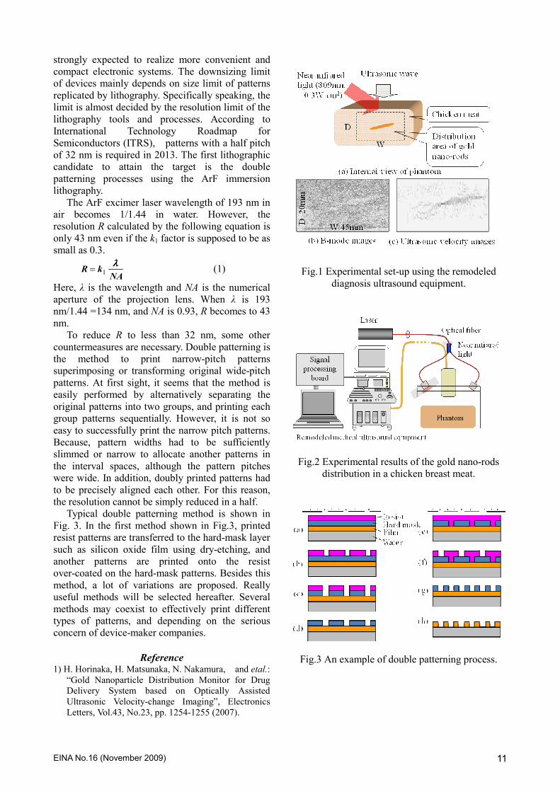
Figure 1 shows the experimental setup in this
study. The center in the picture is the remodeled
diagnostic ultrasonic equipment. This equipment is
attached “the signal processing board” to transfer
RF echo data to the personal computer. The
experimental setup was applied to obtain the
tomography of the phantom including gold
nano-rods as an absorbing material. Figure 2 (a)
shows the internal view of the phantom. The
phantom was made of the chicken breast meat
which contained nano-rods mixed with an agar-gel.
Gold nanorods located at 10 mm depth of the
chicken meat. The array transducer was set above
the chicken meat. The laser diode operating at 809
nm which was close to the gold nano-rods
absorption peak was used as a light source.
Waveforms of RF signal of ultrasonic array
transducer obtained before and after illumination
were stored and their partial shifts were calculated
by a personal computer. The ultrasonic velocity
change images were constructed from the partial
shift of waveform of every scan line. Figure 2 (b)
shows the B-mode image of the phantom. From the
B-mode image, it is difficult to detect the
distribution of nano-rods gel. Figure 2 (c) shows the
ultrasonic velocity change image which was taken
at 30s in the exposure time. The distribution area of
nano-rods appears clearly in the ultrasonic velocity
change image.
Possibility as a monitor of nanoparticle
distribution in living organisms was shown by
experimental results. If the present imaging method
is used as a drug delivery monitor of the gold
nano-rods, it may be possible to obtain spatial
information about malignant tumors in deeper
regions.
The second topic is double patterning processes
using the ArF immersion lithography. Further
miniaturization of semiconductor devices is
EINA No.16 (November 2009) 11
strongly expected to realize more convenient and
compact electronic systems. The downsizing limit
of devices mainly depends on size limit of patterns
replicated by lithography. Specifically speaking, the
limit is almost decided by the resolution limit of the
lithography tools and processes. According to
International Technology Roadmap for
Semiconductors (ITRS), patterns with a half pitch
of 32 nm is required in 2013. The first lithographic
candidate to attain the target is the double
patterning processes using the ArF immersion
lithography.
The ArF excimer laser wavelength of 193 nm in
air becomes 1/1.44 in water. However, the
resolution R calculated by the following equation is
only 43 nm even if the k1 factor is supposed to be as
small as 0.3.
NAkR
λλλλ1= (1)
Here, λ is the wavelength and NA is the numerical
aperture of the projection lens. When λ is 193
nm/1.44 =134 nm, and NA is 0.93, R becomes to 43
nm.
To reduce R to less than 32 nm, some other
countermeasures are necessary. Double patterning is
the method to print narrow-pitch patterns
superimposing or transforming original wide-pitch
patterns. At first sight, it seems that the method is
easily performed by alternatively separating the
original patterns into two groups, and printing each
group patterns sequentially. However, it is not so
easy to successfully print the narrow pitch patterns.
Because, pattern widths had to be sufficiently
slimmed or narrow to allocate another patterns in
the interval spaces, although the pattern pitches
were wide. In addition, doubly printed patterns had
to be precisely aligned each other. For this reason,
the resolution cannot be simply reduced in a half.
Typical double patterning method is shown in
Fig. 3. In the first method shown in Fig.3, printed
resist patterns are transferred to the hard-mask layer
such as silicon oxide film using dry-etching, and
another patterns are printed onto the resist
over-coated on the hard-mask patterns. Besides this
method, a lot of variations are proposed. Really
useful methods will be selected hereafter. Several
methods may coexist to effectively print different
types of patterns, and depending on the serious
concern of device-maker companies.
Reference
1) H. Horinaka, H. Matsunaka, N. Nakamura, and etal.:
“Gold Nanoparticle Distribution Monitor for Drug
Delivery System based on Optically Assisted
Ultrasonic Velocity-change Imaging”, Electronics
Letters, Vol.43, No.23, pp. 1254-1255 (2007).
Fig.1 Experimental set-up using the remodeled
diagnosis ultrasound equipment.
Fig.2 Experimental results of the gold nano-rods
distribution in a chicken breast meat.
Fig.3 An example of double patterning process.
EINA No.16 (November 2009) 12
Metal and Ceramics (MC)
Chairperson: Ataru Ichinose (CRIEPI)
Secretary: Akio Kimura (The Furukawa Electric Co., Ltd.)
Assistant Secretary: Yasuzo Tanaka (International Superconductivity
Technology Center)
Welcome to our Technical Committee on Metal and Ceramics (TC-MC) in the Institute of
Electrical Engineers of Japan (IEEJ). It is expected the TC-MC to promote the electrical
materials and related technologies. Therefore, we have the pleasure to inform activities of
the TC-MC and to communicate with each other.
Mission of TC-MC
The metal and ceramic materials are
indispensable to electric and electronic fields and in
front of advanced technologies all the time. In the
twenty-first century, many advanced technologies
need promising materials such as new materials or
new functional materials for the diversification and
renewable society. Therefore, the metal and ceramic
materials are significant still more and will play an
important role as a pioneer in the future.
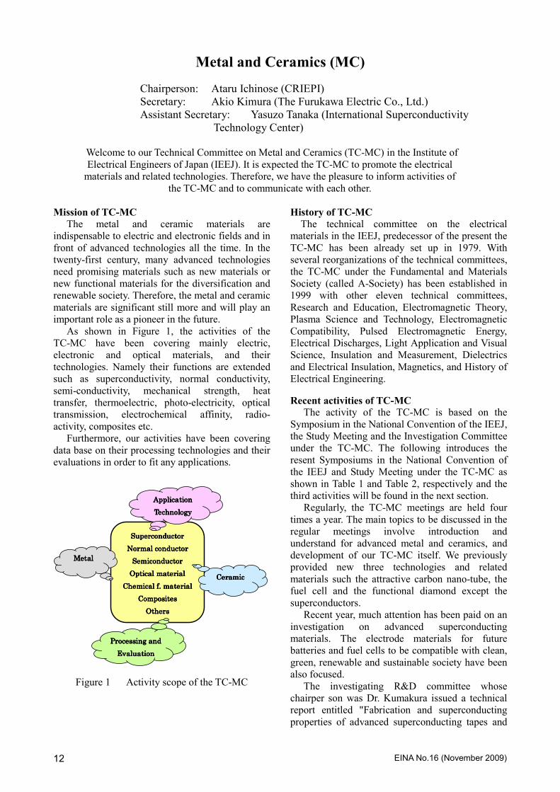
As shown in Figure 1, the activities of the
TC-MC have been covering mainly electric,
electronic and optical materials, and their
technologies. Namely their functions are extended
such as superconductivity, normal conductivity,
semi-conductivity, mechanical strength, heat
transfer, thermoelectric, photo-electricity, optical
transmission, electrochemical affinity, radio-
activity, composites etc.
Furthermore, our activities have been covering
data base on their processing technologies and their
evaluations in order to fit any applications.
Figure 1 Activity scope of the TC-MC
History of TC-MC
The technical committee on the electrical
materials in the IEEJ, predecessor of the present the
TC-MC has been already set up in 1979. With
several reorganizations of the technical committees,
the TC-MC under the Fundamental and Materials
Society (called A-Society) has been established in
1999 with other eleven technical committees,
Research and Education, Electromagnetic Theory,
Plasma Science and Technology, Electromagnetic
Compatibility, Pulsed Electromagnetic Energy,
Electrical Discharges, Light Application and Visual
Science, Insulation and Measurement, Dielectrics
and Electrical Insulation, Magnetics, and History of
Electrical Engineering.
Recent activities of TC-MC
The activity of the TC-MC is based on the
Symposium in the National Convention of the IEEJ,
the Study Meeting and the Investigation Committee
under the TC-MC. The following introduces the
resent Symposiums in the National Convention of
the IEEJ and Study Meeting under the TC-MC as
shown in Table 1 and Table 2, respectively and the
third activities will be found in the next section.
Regularly, the TC-MC meetings are held four
times a year. The main topics to be discussed in the
regular meetings involve introduction and
understand for advanced metal and ceramics, and
development of our TC-MC itself. We previously
provided new three technologies and related
materials such the attractive carbon nano-tube, the
fuel cell and the functional diamond except the
superconductors.
Recent year, much attention has been paid on an
investigation on advanced superconducting
materials. The electrode materials for future
batteries and fuel cells to be compatible with clean,
green, renewable and sustainable society have been
also focused.
The investigating R&D committee whose
chairper son was Dr. Kumakura issued a technical
report entitled "Fabrication and superconducting
properties of advanced superconducting tapes and
SuperconductorSuperconductorSuperconductorSuperconductor
NormalNormalNormalNormal conductorconductorconductorconductor
SemiconductorSemiconductorSemiconductorSemiconductor
OpticalOpticalOpticalOptical materialmaterialmaterialmaterial
ChemicalChemicalChemicalChemical f.f.f.f. materialmaterialmaterialmaterial
CompositesCompositesCompositesComposites
OthersOthersOthersOthers
CeramicCeramicCeramicCeramic
MetalMetalMetalMetal
ProcessingProcessingProcessingProcessing andandandand
EvaluationEvaluationEvaluationEvaluation
ApplicationApplicationApplicationApplication
TechnologyTechnologyTechnologyTechnology

EINA No.16 (November 2009) 13
wires”. This report won IEEJ outstanding technical
report award in 2009. The forum using this
technical report as a text book was held at CRIEPI
on March 2008.
Activities of investigation committee in TC-MC
At present, there is one investigating R&D
committee under TC-MC as shown in Table 3, the
name of which is “Structure and composition of
advanced superconducting materials”. The
chairperson and secretary are Prof. Jyun-ichi
Shimoyama (University of Tokyo) and Dr. Hiraku
Ogino (University of Tokyo), respectively.
Regularly, there are four meetings a year.
The meetings discuss fabrication technologies
and evaluations on electromagnetic, thermal and
mechanical properties mainly for Nb3Al conductors,
Bi-based oxide superconductors, MgB2 conductors
and Y-based oxide superconductors. Most expecting
investigation results are fabrication technologies to
obtain the high performance and its possibility at a
viewpoint of microstructures and chemical
composition for various superconducting materials
such as Nb3Al conductors, Bi-based oxide
superconductors, MgB2 conductors and Y-based
oxide superconductors. And their cost performances
as the practical superconductors and their applied
technologies to such as persistent current
mode-coils, cables, transformers, fault current
limiters and so on. The committee is planning a
study meeting related with the advanced
superconducting materials on March 2010.
Table 1 Symposiums in the National Convention of the IEEJ
Theme Date Site
High magnetic field characteristics and indications for
magnetic application of the High-Tc superconducting
wires
2008.03.19 Fukuoka Institute of
Technology
Development and problem of the high-efficiency solar
cell 2009.03.19 Hokkaido University
Metal and ceramic materials in energy strange systems
(Planning) 2010.3. Meiji University
Table 2 Study Meetings in TC-MC
Theme Date Site
Development of advanced superconducting wires and
their future problems 2008.03.14 CRIEPI
Recent research progress in structure, composition and
characterization of advanced superconducting materials 2010.3. Suspense
Table 3 Investigation Committees under the TC-MC
Research Subject Chairperson (Affiliation) Period Remarks
Wire and conductor forming of
sperconducting materials Shirabe Akita (CRIEPI) 2001.10-2004.09 Close
Fabrication technologies and
characterization of advanced
superconducting materials
Hiroaki Kumakura (NIMS) 2004.10-2007.09 Close
Structure, composition and characterization
of advanced superconducting materials
Jyun-ichi Shimoyama
(University of Tokyo) 2008.10-2011.09 Open
EINA No.16 (November 2009) 14
Instrumentation and Measurement (IM)
Chairperson: Kazuo Tanabe (CRIEPI)
Vice- Chairperson: Yoshitaka Sakumoto (JEMIC), Akihito Otani (Anritsu)
Secretaries: Terumitsu Shirai (JEMIC)
The Technical Committee of Instrumentation
and Measurement of IEEJ was set up in Jan. 1980,
succeeding the Committee on Electronics
Instrumentation and Measurement. The field of
instrumentation and measurement technology is
very wide and has a long history. The activity of our
committee is always influenced by the
technological trend in the era. The early activities of
this committee have mainly focused upon the
presentation and discussion of studies and
researches in the fields of electrical standards and
precise measurement in various electrical fields. It
is the reason that our committee is now categorized
in the society A (Fundamentals and Materials) of
IEEJ. Technological contents in our committee have,
however, gradually shifted to various electrical and
electronic fields.
Annual activities in the technical committee of
instrumentation and measurement have roughly
introduced as follows.
i) The general meeting of the committee is
held four times every year for discussing
the various activities of the committee.
Fifteen members including chairperson,
two secretaries, and an assistant-secretary
constitute the committee.
ii) The workshops for the presentation and
discussion of studies and researches take
place almost every month in principle as a
main activity of the committee.
iii) The visit of various professional facilities is
planned to carry out once or twice a year.
The actual subject issues in the workshop are the
presentation and the discussion of extensive
electronic instrumentation and measurement
technologies including;
# Ultra-high speed measuring method employing optical technology
# Electro-magnetic measurement for ensuring
EMC
# High precision measurement in frequencies and
time domain for radio-controlled watches, GPS,
and navigation
# Application of SQUID and MRI to
bio-measurement
# Bio-electronic measurement applicable to the
welfare field in society shifted to the aged
# Magnetic measurement related to magnetic
sensors
# Resolving factors causing uncertainty and
development of its reducing method for
establishment of electrical standards
The workshops mainly take place at Tokyo area,
and sometimes in Saga and Miyazaki (Kyushu
Island), in Osaka and in others. The themes of
presentation in the workshop are usually focused on
the electromagnetic measurement, the remote
control instrumentation, the application of optical
measurement, the biological electronic
measurement, the time and frequency measurement,
the application of magnetic measurement and so on,
but in several workshops, miscellaneous subjects
are acceptable to present and discuss there.
The number of annual presentation in the
workshops is around 70 titles. The workshop is
supported by IEEE IM and sometimes by other
organization.
Recently, the committee planed a special
volume on “Measurement Technology for Safety”
and then the volume including eight papers was
published on August 2009. The titles and authors
are as follows;
# Research into Warning Time Optimum Control
for Level Crossing with a Continuous Type
Train Location Detector using Crossed
Inductive Wires (T. Matsumura & T. Ono)
# Real-Scale Measurement Results for Audible
Noise from AC Overhead Transmission Lines
and Prediction Formula in Heavy Rain (K.
Tanabe)
# Development of Isolated Travel Sensor for
High-voltage Switchgear (A. Shiratsuki, T.
Mori, H. Kohyama, H. Nakajima, T.
Nakashima, T. Oka, & K. Sumi)
# Flame Imaging for Safety Surveillance (T.
Fukuchi)
# An Error Estimate of the VHF Broadband
Digital Interferometer (Y. Nakamura, T.
Morimoto, T. Ushio, & Z. Kawasaki)
# Continuous Measurement of Amplitude
Probability Distribution and Applications to
Pulses of Low Occurrence Frequency (S.
Arakawa, S. Ronte, T. Otsuka, H. Aso, & M.
Uchino)
# Suppression of Clutter near Port by S-Band
Radar (S. Ishii & S. Sayama)
# Weathering State Independent Rock Type
EINA No.16 (November 2009) 15
Classification using Textural Features (E.
Momma, H. Ishii, & T. Ono)
Our committee website (http://202.235.159.197/
~aim/) also assists to understand our activity.
Written by Dr. Kazuo Tanabe (Central Research
Institute of Electric Power Industry, CRIEPI),
Chairman, e-mail: [email protected]
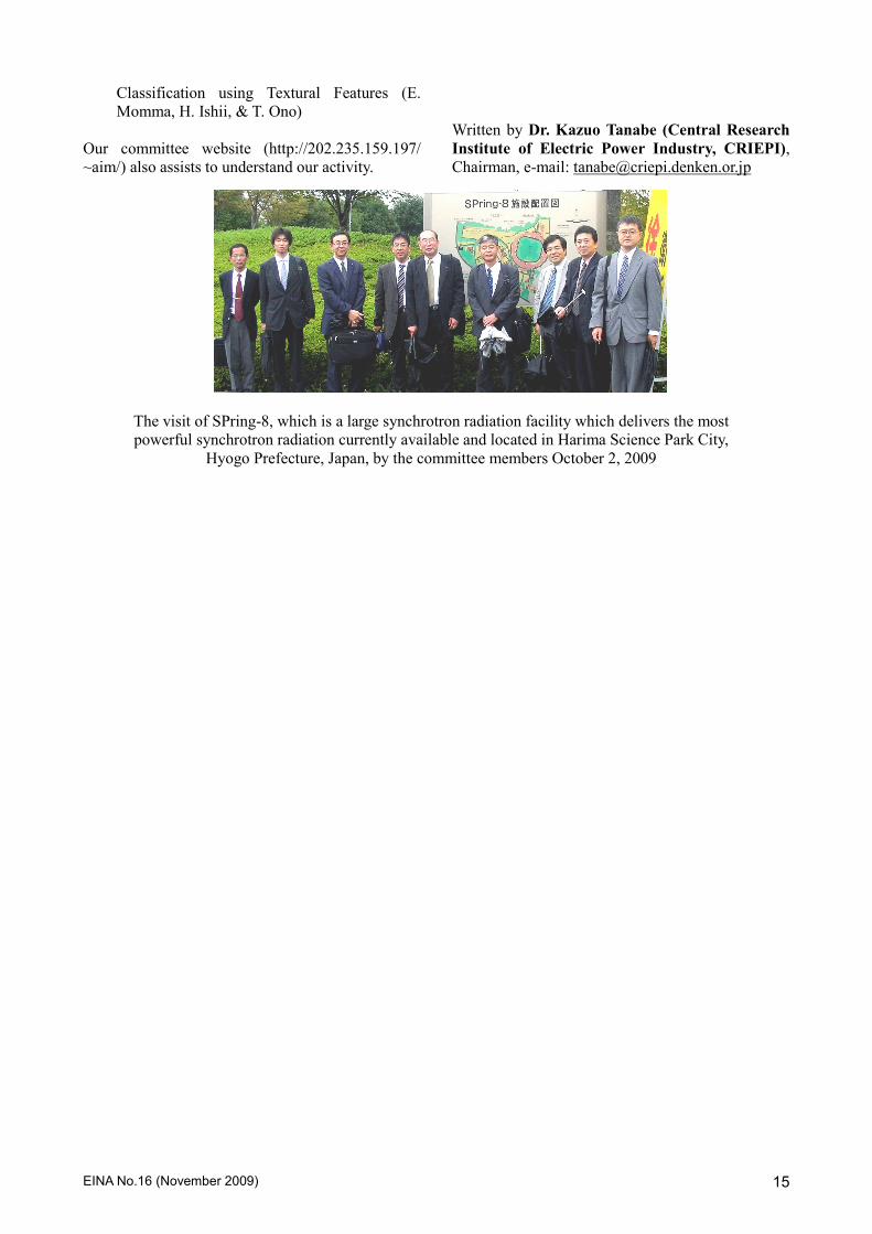
The visit of SPring-8, which is a large synchrotron radiation facility which delivers the most
powerful synchrotron radiation currently available and located in Harima Science Park City,
Hyogo Prefecture, Japan, by the committee members October 2, 2009
EINA No.16 (November 2009) 16
IEC and CIGRE Japanese National Committees
Related to Electrical Insulating Materials
IEC TC15 Japanese National Committee
Chairperson: Yoshiaki Yamano (Chiba University)
Secretary: Yoshio Wakashima (Japan Electrical Safety & Environment Technology Lab.)
Associate Secretary: Akihiro Kawaguchi (Japan Electrical Safety & Environment Technology Lab.)
The task for IEC TC15 is to prepare
international standards including specifications for
solid electrical insulating materials alone and in
simple combinations. This includes coatings which
are applied in the liquid state but cure to solids,
such as varnishes and coatings.
TC15 establishes definitions, general
requirements and specification sheets for individual
types of materials. The standards include test
methods and guidance where these are required for
the specifications. The current activities of TC15
are carried out in 5 working groups (WGs) and 4
maintenance teams (MTs), and more than 160
standards are published and 23 projects are working
in progress.
Japanese national committee for TC15C held
three meetings in last year. Over 30 documents for
standardization have been sent from IEC Central
Office, including CD, CDV and FDIS, all of which
were circulated to the member of the Japanese
National committee and discussed. Totally more
than 80 reports or documents including voting
results, compiled comments and reports concerning
to the management were circulated.
For the activities on the WGs in TC15, the
experts from Japan participate in MT3 (Plastic
films), WG5 (flexible insulating sleeving), WG7
(resins and varnish) and WG9 (Cellulosic
materials).
Japanese national committee is participating to
the standardization for new insulating materials as
well as the conventional ones to develop the
international standardization in the field of
insulating materials.
TC15 meeting has been annually held. The
meeting of this year was held on May in London. 6
members from Japan participated to MT/WG
meetings and the plenary meeting.
IEC TC112 Japanese National Committee
Chairperson: Noriyuki Shimizu (Meijo University)
Vice Chair: Tatsuki Okamoto (CRIEPI)
Secretaries : Hiroaki Uehara (Kanto Gakuin University)
Hiroya Homma (CRIEPI)
The International Electrotechnical
Commission (IEC) is the leading global
organization that prepares and publishes
international standards for all electrical,
electronic and related technologies. The IEC
has 94 Technical Committees (TCs) and 80
Subcommittees (SCs). TC 112 was established
in 2005 May by the merger of SC 15 E
“Insulating Materials - Methods of Test” and
“TC 98 Electrical Insulation Systems”.
The title, the scope and the horizontal safety
function of Technical Committee 112 (TC112)
at the present time are as follow.
Title: Evaluation and qualification of electrical
insulating materials and systems
Scope: To prepare International Standards
covering methods of evaluation and
qualification for electrical and electronic
insulating materials, and electrical insulation
systems.
Horizontal Safety Function: Test methods for
resistance to tracking.
EINA No.16 (November 2009) 17
The participant members and the observer
members are 21 countries and 7 countries (as of
September 1, 2009) respectively. Japan is one
of the participant members. TC112 has 80
publications.
The chairman of TC112 was recently
changed. The new chairman (from October 1,
2009 to September 30, 2015) is Mr. R.C.Wicks
(USA). The secretary is Mr. B.Goettert
(Germany).
The TC112 Japanese National Committee
(JNC) was established in October 2005. The
42 experts from universities, research institutes
and industries serve as the members of the
TC112 JNC. The officers are as follows:
Chair: Prof. N. Shimizu (Meijo University)
Vice Chair: Dr. T.Okamoto (Central
Research Institute of Electric Power Industry)
Secretaries : Prof. H. Uehara (Kanto Gakuin
University) and Dr. H.Homma (Central
Research Institute of Electric Power Industry)
TC112 has 8 working groups WG1-8. It
should be mentioned that the three convenors of
WG2, WG7 and WG8 are from our JNC.
Corresponding to these WGs in the
international area, JNC has also 8 WGs in the
domestic area. WGs are shown in Table 1
below with names of covenors and chiefs in
Japan.
Table 1 WGs in TC112 and Convenors
and Chiefs in JNC
WG. Title Convenor /
Chief in JNC
WG 1 Thermal
Endurance
Prof. G.C. Montanari,
Italy / Mr.N.Nakamura
WG 2 Radiation Prof. H.Kudo, Japan /
Prof. H.Kudo
WG 3 Electric
Strength
Prof. K.Stimper, Germany / Prof. K.Kimura
WG 4 Dielectric / Resistive Properties
Mr. H.Haupt, Germany
/ Prof. E.Watanabe
WG 5 Tracking Dr. J.Winter, Germany /
Dr. H.Homma
WG 6
General Methods of Evaluation of Electrical Insulation
Prof. J.Smit,
Netherlands /
Mr.T.Sakano
WG 7 Statistics Dr. T.Okamoto, JP /
Dr. T.Okamoto
WG 8 Various
Material
Properties
Prof. N.Shimizu, JP /
Prof. N.Shimizu
Some projects are working to establish new
standards under WGs. Currently TC112 has 4
PWI (preliminary work item) projects. Two
project leaders (PLs) are from our JNC.
-Electrical insulating materials and systems -
Electrical measurement of partial discharges
(PD) under short rise time and repetitive
voltage impulses
WG 3 PL: Prof. K. Kimura (Japan)
-Calibration of space change measuring
equipment
WG8 PL: Prof. Y. Tanaka (Japan)
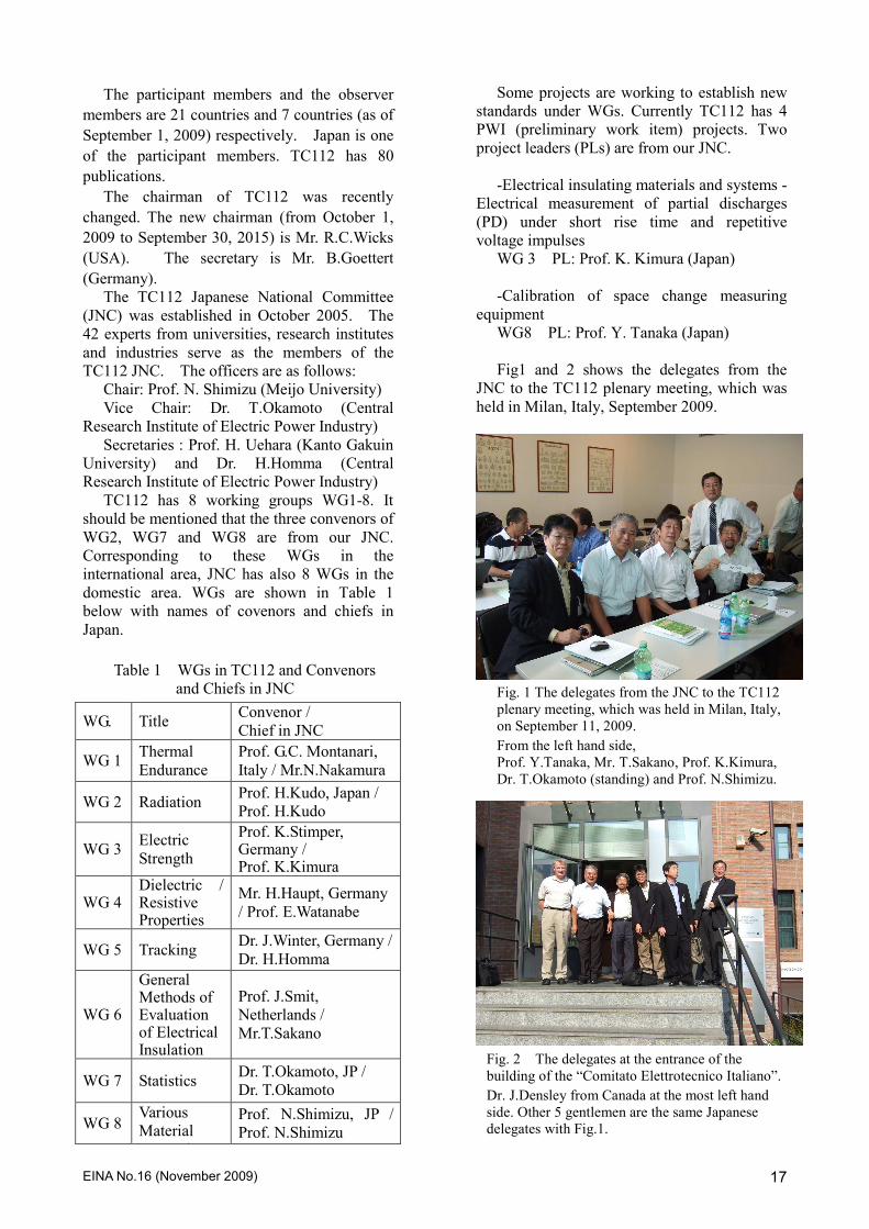
Fig1 and 2 shows the delegates from the
JNC to the TC112 plenary meeting, which was
held in Milan, Italy, September 2009.
Fig. 1 The delegates from the JNC to the TC112
plenary meeting, which was held in Milan, Italy,
on September 11, 2009.
From the left hand side,
Prof. Y.Tanaka, Mr. T.Sakano, Prof. K.Kimura,
Dr. T.Okamoto (standing) and Prof. N.Shimizu.
Fig. 2 The delegates at the entrance of the
building of the “Comitato Elettrotecnico Italiano”.
Dr. J.Densley from Canada at the most left hand
side. Other 5 gentlemen are the same Japanese
delegates with Fig.1.

EINA No.16 (November 2009) 18
CIGRE SC D1 Japanese National Committee ( Materials and Emerging Test Techniques )
Chairperson: Masayuki Nagao (Toyohashi University of Technology)
Secretary: Toshio Shimizu (Toshiba Corporation)
Naohiro Hozumi (Aichi Institute of Technology)
Assistant Secretary: Tsuguhiro Takahashi (CRIEPI)
CIGRE (International Council on Large Electric
Systems) has 16 Study Committees (SC) belonging
to each of following 4 categories: A (Equipment), B
(Subsystems), C (Systems) and D (Horizontal).
Among them, our SC D1 has a horizontal character
and contributes to other CIGRE SC's. Last year SC
D1 changed the theme to "Materials and Emerging
Test Techniques" from "Materials and Emerging
Technologies", because “Emerging Technologies”
are too wide and are considered not to be only for
SC D1. This theme change adjusted the matching of
the theme and our main field of activities in better
direction. The activity of CIGRE SC’s is principally
research oriented one, while some of them are
closely related to the activities of IEC Committees
which publish and maintain the International
Standards in the field of the Electrotechnology.
SC D1 has now following 5 Advisory Groups
(AG): CSAG (Customer and Strategic related), AG
D1.01 (Insulating Liquids), AG D1.02 (High
Voltage Testing and Diagnostic), AG D1.03
(Insulating Gases) and AG D1.04 (Insulating
Solids). Previous AG D1.05 (Capacitors) became
Working Groups (WG) D1.05 and AG D1.06
(Emerging Technologies) was disbanded. In 2009
CIGRE SC D1 Budapest meeting, SC D1 has
started 2 new WG’s: WG D1.27 (Material
Properties for New and Nonceramic Insulation)
chaired by Prof.Kindersberger and WG D1.28
(Optimized Gas-insulated Systems by Advanced
Dielectric Coatings and Functionally Graded
Materials) chaired by Dr.Hama. SC D1 now
consists of 5 AG’s and 15 WG’s: the above new
WG’s as well as the 13 existed following WG’s:
WG D1.01 (Liquid Impregnated Systems for
Transformers), WG D1.05 (Capacitrs), WG D1.07
(Solid Insulating Materials for Rotating Machines),
WG D1.15 (HTSC-Material Applications &
Cooling), WG D1.17 (HV Asset Condition
Assessment Tools, Data Quality and Expert
Systems), WG D1.18 (Emerging Technologies in
Power Systems), SCTF D1.19 (Solid Insulation
Endurance under Repetitive Transient Voltages),
SCTF D1.20 (Water Tree Detection in XLPE
insulation), WG D1.23 (Diagnostics and
Accelerated Life Endurance Testing of Polymeric
Materials for HVDC Application), WG D1.24
(Potential of Polymer Nanocomposites as Electrical
Insulation for Highly Stressed Insulation Material
in AC and DC Application), WG D1.25
(Application Guide for PD Detection in GIS using
UHF or Acoustic Methods), WG D1.26 (Basic
Principles to Determinate Methane Content of
Cross-linked Solid Insulation of MV and HV
Cables) and WG D1.33 (High Voltage Test and
Measuring Techniques).
The preferential subjects for the 2010 SC D1
Paris group meeting are PS1: New materials for improved efficiency and sustainability of AC & DC power equipment (Nanomaterials, biodegradable materials, New gas compositions, Recyclable materials, Innovative polymers, HTSC), PS2: Challenges for testing and diagnostics (New requirements for ultra high voltage, Interpretation of diagnostic results for condition assessment, New test and monitoring methods), PS3: Endurance of materials especially in harsh electrical and physical environments (Off-shore applications, Repetitive transients, load cycling, thermal overload, nuclear environment). From Japan, following 3 papers are accepted: “Endurance of polymeric insulating materials in nuclear power plants and needs for condition monitoring of electrical cables” by Y. Ohki, et al, “Application of new solid insulating materials and new gas compositions to future advanced gas insulated systems” by H. Hama, et al., “Experimental research on the feasibility of biodegradable polymeric insulating materials” by Y. Ohki, et al. The next 2010 meeting is scheduled to be held
during CIGRE Paris meeting in Paris, France on
August 22-27, 2010. In this 2010 Paris meeting the
chairman of SC D1 will be changed from
Prof.Gockenbach to Prof.Kindersberger. The 2011
SC D1 meeting was decided to be held in Kyoto,
Japan in conjunction with SC A2 (Transformer)
The Japanese National SC D1 has usually 3 or 4
meetings a year.
Prof. Masayuki NAGAO
Toyohashi University of Technology
Tempaku, Toyohashi, 441-8580 Japan
E-mail: [email protected]
TEL: +81-532-44-6725
Skype ID: nagao
EINA No.16 (November 2009) 19
RESEARCH ACTIVITIES AND TECHNICAL
EXCHANGES IN ASIAN COUNTRIES
Conference Records
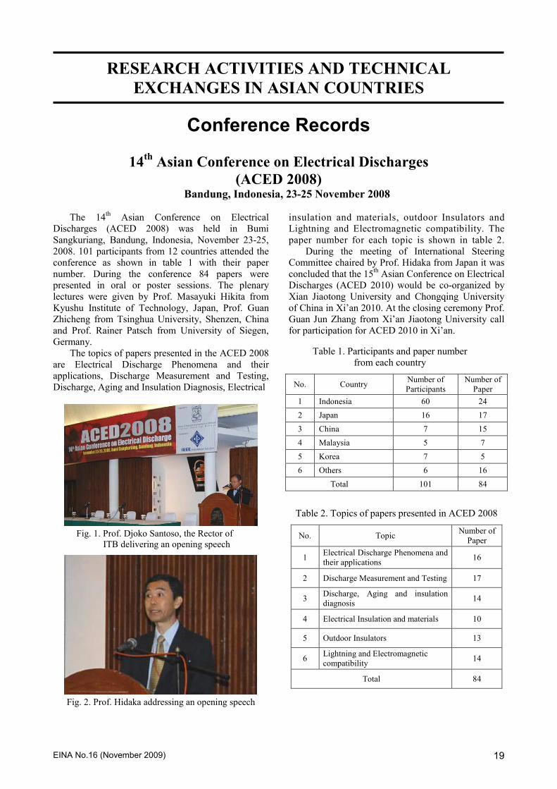
14th Asian Conference on Electrical Discharges
(ACED 2008) Bandung, Indonesia, 23-25 November 2008
The 14th Asian Conference on Electrical
Discharges (ACED 2008) was held in Bumi
Sangkuriang, Bandung, Indonesia, November 23-25,
2008. 101 participants from 12 countries attended the
conference as shown in table 1 with their paper
number. During the conference 84 papers were
presented in oral or poster sessions. The plenary
lectures were given by Prof. Masayuki Hikita from
Kyushu Institute of Technology, Japan, Prof. Guan
Zhicheng from Tsinghua University, Shenzen, China
and Prof. Rainer Patsch from University of Siegen,
Germany.
The topics of papers presented in the ACED 2008
are Electrical Discharge Phenomena and their
applications, Discharge Measurement and Testing,
Discharge, Aging and Insulation Diagnosis, Electrical
Fig. 1. Prof. Djoko Santoso, the Rector of
ITB delivering an opening speech
Fig. 2. Prof. Hidaka addressing an opening speech
insulation and materials, outdoor Insulators and
Lightning and Electromagnetic compatibility. The
paper number for each topic is shown in table 2.
During the meeting of International Steering
Committee chaired by Prof. Hidaka from Japan it was
concluded that the 15th Asian Conference on Electrical
Discharges (ACED 2010) would be co-organized by
Xian Jiaotong University and Chongqing University
of China in Xi’an 2010. At the closing ceremony Prof.
Guan Jun Zhang from Xi’an Jiaotong University call
for participation for ACED 2010 in Xi’an.
Table 1. Participants and paper number
from each country
No. Country Number of
Participants
Number of
Paper
1 Indonesia 60 24
2 Japan 16 17
3 China 7 15
4 Malaysia 5 7
5 Korea 7 5
6 Others 6 16
Total 101 84
Table 2. Topics of papers presented in ACED 2008
No. Topic Number of
Paper
1 Electrical Discharge Phenomena and
their applications 16
2 Discharge Measurement and Testing 17
3 Discharge, Aging and insulation
diagnosis 14
4 Electrical Insulation and materials 10
5 Outdoor Insulators 13
6 Lightning and Electromagnetic
compatibility 14
Total 84
EINA No.16 (November 2009) 20
Fig. 3. Prof. Hikita delivering an invited speech
Fig. 4. Prof. Guan Zhicheng at plenary speech
Fig. 5. Prof. Patsch, Dr. Suwarno and
Prof. Sinisuka at a break time
Fig. 6. Dance performance at dinner party
Prepared by: Prof. Suwarno
Bandung Institute of Technology
Indonesia
Fig. 7. All participants of the ACED 2008

EINA No.16 (November 2009) 21
CIGRE Workshop on Test Techniques and
Procedures for HTS Power Applications
Naoki Hayakawa (Nagoya University, Japan)
CIGRE Workshop on Test Techniques and
Procedures for HTS Power Applications was held in
Nagoya University on May 13-15, 2009. This
Workshop was hosted by CIGRE SC D1 WG 15
“Superconducting and Insulating Materials for HTS
Power Applications” (Convenor: Prof. Hitoshi Okubo,
Nagoya University). The number of participants was
88 (Japanese: 69, foreigners: 19) from 11 countries
(Japan, USA, Germany, China, France, Italy,
Netherlands, Brazil, Australia, Egypt, Korea). The
purpose of this Workshop is to exchange the latest
world progress in HTS power applications and their
test techniques with 4 plenary lectures and 19
presentations on cable, power equipment, common
test techniques, fault current limiters. The program
and PDF files of plenary lectures and presentations
can be downloaded from
http://www.okubo.nuee.nagoya-u.ac.jp/CIGRE/.
Figure 1 shows a group photograph of the Workshop
participants.
In the afternoon on May 14, the meeting of
CIGRE SC D1 WG 15 was held with 24 participants
from 10 countries (Figure 2). The session chairmen of
the Workshop gave a short summary of the highlights
in their session. Following the summary, a discussion
on present and future links from WG D1.15 to other
CIGRE WGs (A1: Rotating Electrical Machines, A2:
Transformers, A3.23: Fault Current Limiters, B1:
Insulated Cables) and activities continued. There was
consensus that strong links between the different
CIGRE WGs are meaningful and should be further
established. After the meeting, a banquet was held in a
Japanese garden, Tokugawaen (Figure 3).
Figure 1
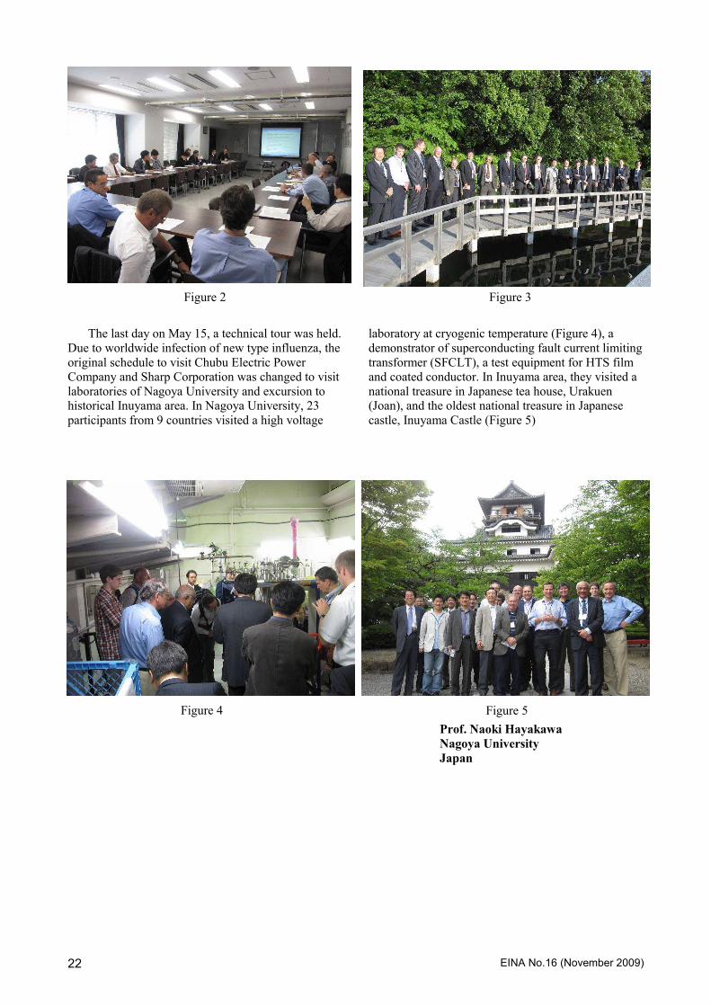
EINA No.16 (November 2009) 22
The last day on May 15, a technical tour was held.
Due to worldwide infection of new type influenza, the
original schedule to visit Chubu Electric Power
Company and Sharp Corporation was changed to visit
laboratories of Nagoya University and excursion to
historical Inuyama area. In Nagoya University, 23
participants from 9 countries visited a high voltage
laboratory at cryogenic temperature (Figure 4), a
demonstrator of superconducting fault current limiting
transformer (SFCLT), a test equipment for HTS film
and coated conductor. In Inuyama area, they visited a
national treasure in Japanese tea house, Urakuen
(Joan), and the oldest national treasure in Japanese
castle, Inuyama Castle (Figure 5)
Prof. Naoki Hayakawa
Nagoya University
Japan
Figure 3 Figure 2
Figure 4 Figure 5
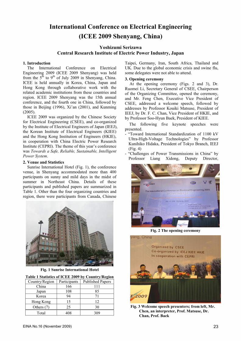
EINA No.16 (November 2009) 23
International Conference on Electrical Engineering
(ICEE 2009 Shenyang, China)
Yoshizumi Serizawa
Central Research Institute of Electric Power Industry, Japan
1. Introduction The International Conference on Electrical
Engineering 2009 (ICEE 2009 Shenyang) was held
from the 5th to 9
th of July 2009 in Shenyang, China.
ICEE is held annually in Korea, China, Japan and
Hong Kong through collaborative work with the
related academic institutions from these countries and
region. ICEE 2009 Shenyang was the 15th annual
conference, and the fourth one in China, followed by
those in Beijing (1996), Xi’an (2001), and Kunming
(2005).
ICEE 2009 was organized by the Chinese Society
for Electrical Engineering (CSEE), and co-organized
by the Institute of Electrical Engineers of Japan (IEEJ),
the Korean Institute of Electrical Engineers (KIEE)
and the Hong Kong Institution of Engineers (HKIE),
in cooperation with China Electric Power Research
Institute (CEPRI). The theme of this year’s conference
was Towards a Safe, Reliable, Sustainable, Intelligent
Power System.
2. Venue and Statistics
Sunrise International Hotel (Fig. 1), the conference
venue, in Shenyang accommodated more than 400
participants on sunny and mild days in the midst of
summer in Northeast China. Details of these
participants and published papers are summarized in
Table 1. Other than the four organizing countries and
region, there were participants from Canada, Chinese
Taipei, Germany, Iran, South Africa, Thailand and
UK. Due to the global economic crisis and swine flu,
some delegates were not able to attend.
3. Opening ceremony At the opening ceremony (Figs. 2 and 3), Dr.
Ruomei Li, Secretary General of CSEE, Chairperson
of the Organizing Committee, opened the ceremony,
and Mr. Feng Chen, Executive Vice President of
CSEE, addressed a welcome speech, followed by
addresses by Professor Kouiki Matsuse, President of
IEEJ, by Dr. F. C. Chan, Vice President of HKIE, and
by Professor Soo-Hyun Baek, President of KIEE.
The following five keynote speeches were
presented.
- “Toward International Standardization of 1100 kV
Ultra-High-Voltage Technologies” by Professor
Kunihiko Hidaka, President of Tokyo Branch, IEEJ
(Fig. 4)
- “Challenges of Power Transmissions in China” by
Professor Liang Xidong, Deputy Director,
Fig. 2 The opening ceremony
Fig. 3 Welcome speech presenters; from left, Mr.
Chen, an interpreter, Prof. Matsuse, Dr.
Chan, Prof. Baek
Fig. 1 Sunrise International Hotel
Table 1 Statistics of ICEE 2009 by Country/Region
Country/Region Participants Published Papers
China 166 111
Japan 108 85
Korea 94 71
Hong Kong 15 12
Others (7) 25 30
Total 408 309
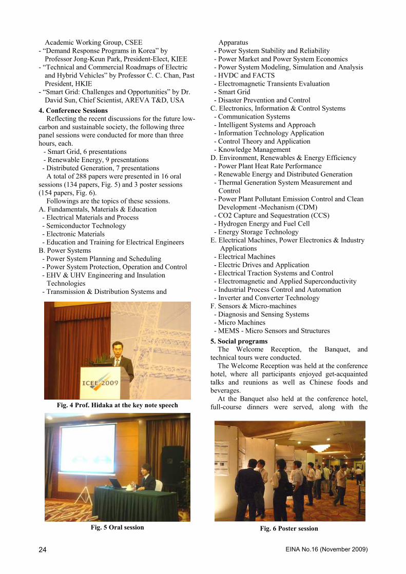
EINA No.16 (November 2009) 24
Academic Working Group, CSEE
- “Demand Response Programs in Korea” by
Professor Jong-Keun Park, President-Elect, KIEE
- “Technical and Commercial Roadmaps of Electric
and Hybrid Vehicles” by Professor C. C. Chan, Past
President, HKIE
- “Smart Grid: Challenges and Opportunities” by Dr.
David Sun, Chief Scientist, AREVA T&D, USA
4. Conference Sessions
Reflecting the recent discussions for the future low-
carbon and sustainable society, the following three
panel sessions were conducted for more than three
hours, each.
- Smart Grid, 6 presentations
- Renewable Energy, 9 presentations
- Distributed Generation, 7 presentations
A total of 288 papers were presented in 16 oral
sessions (134 papers, Fig. 5) and 3 poster sessions
(154 papers, Fig. 6).
Followings are the topics of these sessions.
A. Fundamentals, Materials & Education
- Electrical Materials and Process
- Semiconductor Technology
- Electronic Materials
- Education and Training for Electrical Engineers
B. Power Systems
- Power System Planning and Scheduling
- Power System Protection, Operation and Control
- EHV & UHV Engineering and Insulation
Technologies
- Transmission & Distribution Systems and
Apparatus
- Power System Stability and Reliability
- Power Market and Power System Economics
- Power System Modeling, Simulation and Analysis
- HVDC and FACTS
- Electromagnetic Transients Evaluation
- Smart Grid
- Disaster Prevention and Control
C. Electronics, Information & Control Systems
- Communication Systems
- Intelligent Systems and Approach
- Information Technology Application
- Control Theory and Application
- Knowledge Management
D. Environment, Renewables & Energy Efficiency
- Power Plant Heat Rate Performance
- Renewable Energy and Distributed Generation
- Thermal Generation System Measurement and
Control
- Power Plant Pollutant Emission Control and Clean
Development -Mechanism (CDM)
- CO2 Capture and Sequestration (CCS)
- Hydrogen Energy and Fuel Cell
- Energy Storage Technology
E. Electrical Machines, Power Electronics & Industry
Applications
- Electrical Machines
- Electric Drives and Application
- Electrical Traction Systems and Control
- Electromagnetic and Applied Superconductivity
- Industrial Process Control and Automation
- Inverter and Converter Technology
F. Sensors & Micro-machines
- Diagnosis and Sensing Systems
- Micro Machines
- MEMS - Micro Sensors and Structures
5. Social programs The Welcome Reception, the Banquet, and
technical tours were conducted.
The Welcome Reception was held at the conference
hotel, where all participants enjoyed get-acquainted
talks and reunions as well as Chinese foods and
beverages.
At the Banquet also held at the conference hotel,
full-course dinners were served, along with the
Fig. 6 Poster session
Fig. 4 Prof. Hidaka at the key note speech
Fig. 5 Oral session
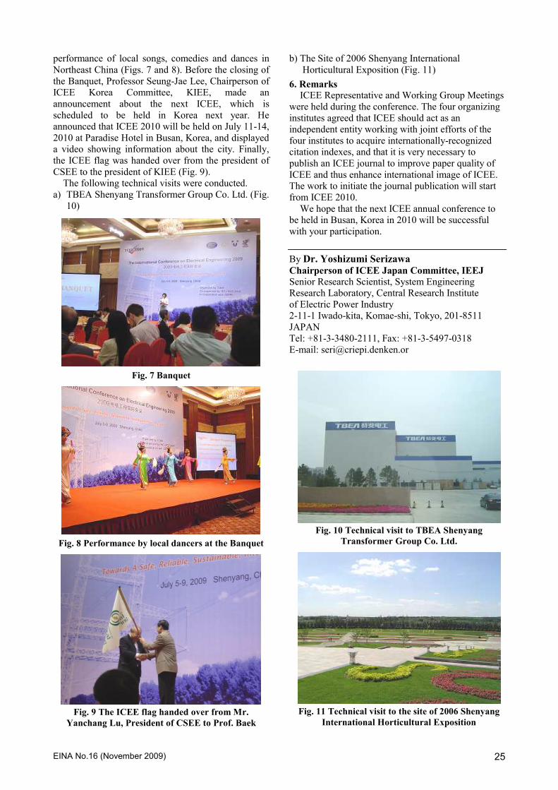
EINA No.16 (November 2009) 25
performance of local songs, comedies and dances in
Northeast China (Figs. 7 and 8). Before the closing of
the Banquet, Professor Seung-Jae Lee, Chairperson of
ICEE Korea Committee, KIEE, made an
announcement about the next ICEE, which is
scheduled to be held in Korea next year. He
announced that ICEE 2010 will be held on July 11-14,
2010 at Paradise Hotel in Busan, Korea, and displayed
a video showing information about the city. Finally,
the ICEE flag was handed over from the president of
CSEE to the president of KIEE (Fig. 9).
The following technical visits were conducted.
a) TBEA Shenyang Transformer Group Co. Ltd. (Fig.
10)
b) The Site of 2006 Shenyang International
Horticultural Exposition (Fig. 11)
6. Remarks ICEE Representative and Working Group Meetings
were held during the conference. The four organizing
institutes agreed that ICEE should act as an
independent entity working with joint efforts of the
four institutes to acquire internationally-recognized
citation indexes, and that it is very necessary to
publish an ICEE journal to improve paper quality of
ICEE and thus enhance international image of ICEE.
The work to initiate the journal publication will start
from ICEE 2010.
We hope that the next ICEE annual conference to
be held in Busan, Korea in 2010 will be successful
with your participation.
By Dr. Yoshizumi Serizawa Chairperson of ICEE Japan Committee, IEEJ
Senior Research Scientist, System Engineering
Research Laboratory, Central Research Institute
of Electric Power Industry
2-11-1 Iwado-kita, Komae-shi, Tokyo, 201-8511
JAPAN
Tel: +81-3-3480-2111, Fax: +81-3-5497-0318
E-mail: [email protected]
Fig. 7 Banquet
Fig. 8 Performance by local dancers at the Banquet
Fig. 9 The ICEE flag handed over from Mr.
Yanchang Lu, President of CSEE to Prof. Baek
Fig. 10 Technical visit to TBEA Shenyang
Transformer Group Co. Ltd.
Fig. 11 Technical visit to the site of 2006 Shenyang
International Horticultural Exposition
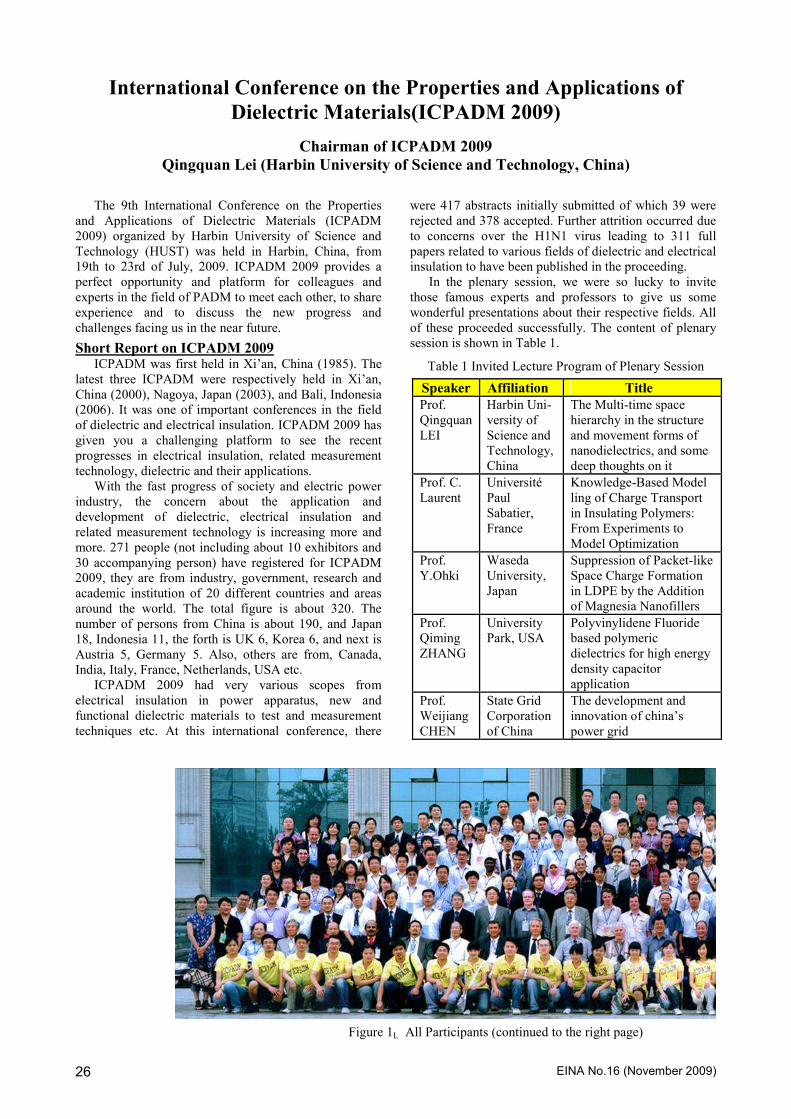
EINA No.16 (November 2009) 26
International Conference on the Properties and Applications of
Dielectric Materials(ICPADM 2009)
Chairman of ICPADM 2009
Qingquan Lei (Harbin University of Science and Technology, China)
The 9th International Conference on the Properties
and Applications of Dielectric Materials (ICPADM
2009) organized by Harbin University of Science and
Technology (HUST) was held in Harbin, China, from
19th to 23rd of July, 2009. ICPADM 2009 provides a
perfect opportunity and platform for colleagues and
experts in the field of PADM to meet each other, to share
experience and to discuss the new progress and
challenges facing us in the near future.
Short Report on ICPADM 2009 ICPADM was first held in Xi’an, China (1985). The
latest three ICPADM were respectively held in Xi’an,
China (2000), Nagoya, Japan (2003), and Bali, Indonesia
(2006). It was one of important conferences in the field
of dielectric and electrical insulation. ICPADM 2009 has
given you a challenging platform to see the recent
progresses in electrical insulation, related measurement
technology, dielectric and their applications.
With the fast progress of society and electric power
industry, the concern about the application and
development of dielectric, electrical insulation and
related measurement technology is increasing more and
more. 271 people (not including about 10 exhibitors and
30 accompanying person) have registered for ICPADM
2009, they are from industry, government, research and
academic institution of 20 different countries and areas
around the world. The total figure is about 320. The
number of persons from China is about 190, and Japan
18, Indonesia 11, the forth is UK 6, Korea 6, and next is
Austria 5, Germany 5. Also, others are from, Canada, India, Italy, France, Netherlands, USA etc.
ICPADM 2009 had very various scopes from
electrical insulation in power apparatus, new and
functional dielectric materials to test and measurement
techniques etc. At this international conference, there
were 417 abstracts initially submitted of which 39 were
rejected and 378 accepted. Further attrition occurred due
to concerns over the H1N1 virus leading to 311 full
papers related to various fields of dielectric and electrical
insulation to have been published in the proceeding.
In the plenary session, we were so lucky to invite
those famous experts and professors to give us some
wonderful presentations about their respective fields. All
of these proceeded successfully. The content of plenary
session is shown in Table 1.
Table 1 Invited Lecture Program of Plenary Session
Speaker Affiliation Title
Prof.
Qingquan
LEI
Harbin Uni-
versity of
Science and
Technology,
China
The Multi-time space
hierarchy in the structure
and movement forms of
nanodielectrics, and some
deep thoughts on it
Prof. C.
Laurent
Université
Paul
Sabatier,
France
Knowledge-Based Model
ling of Charge Transport
in Insulating Polymers:
From Experiments to
Model Optimization
Prof.
Y.Ohki
Waseda
University,
Japan
Suppression of Packet-like
Space Charge Formation
in LDPE by the Addition
of Magnesia Nanofillers
Prof.
Qiming
ZHANG
University
Park, USA
Polyvinylidene Fluoride
based polymeric
dielectrics for high energy
density capacitor
application
Prof.
Weijiang
CHEN
State Grid
Corporation
of China
The development and
innovation of china’s
power grid
Figure 1L All Participants (continued to the right page)
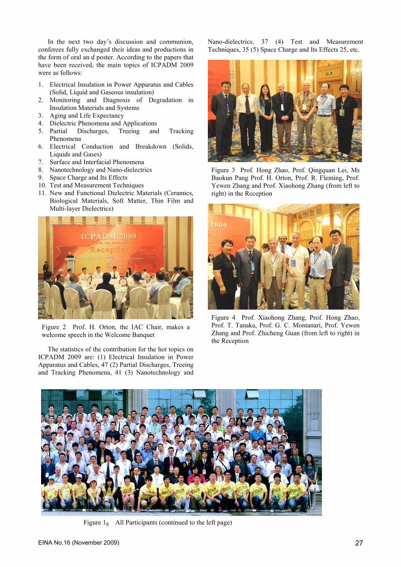
EINA No.16 (November 2009) 27
In the next two day’s discussion and communion,
conferees fully exchanged their ideas and productions in
the form of oral an d poster. According to the papers that
have been received, the main topics of ICPADM 2009
were as follows:
1. Electrical Insulation in Power Apparatus and Cables
(Solid, Liquid and Gaseous insulation)
2. Monitoring and Diagnosis of Degradation in
Insulation Materials and Systems
3. Aging and Life Expectancy
4. Dielectric Phenomena and Applications
5. Partial Discharges, Treeing and Tracking
Phenomena
6. Electrical Conduction and Breakdown (Solids,
Liquids and Gases)
7. Surface and Interfacial Phenomena
8. Nanotechnology and Nano-dielectrics
9. Space Charge and Its Effects
10. Test and Measurement Techniques
11. New and Functional Dielectric Materials (Ceramics,
Biological Materials, Soft Matter, Thin Film and
Multi-layer Dielectrics)
Figure 2 Prof. H. Orton, the IAC Chair, makes a
welcome speech in the Welcome Banquet
The statistics of the contribution for the hot topics on
ICPADM 2009 are: (1) Electrical Insulation in Power
Apparatus and Cables, 47 (2) Partial Discharges, Treeing
and Tracking Phenomena, 41 (3) Nanotechnology and
Nano-dielectrics, 37 (4) Test and Measurement
Techniques, 35 (5) Space Charge and Its Effects 25, etc.
Figure 3 Prof. Hong Zhao, Prof. Qingquan Lei, Ms
Baokun Pang Prof. H. Orton, Prof. R. Fleming, Prof.
Yewen Zhang and Prof. Xiaohong Zhang (from left to
right) in the Reception
Figure 4 Prof. Xiaohong Zhang, Prof. Hong Zhao,
Prof. T. Tanaka, Prof. G. C. Montanari, Prof. Yewen
Zhang and Prof. Zhicheng Guan (from left to right) in
the Reception
Figure 1R All Participants (continued to the left page)
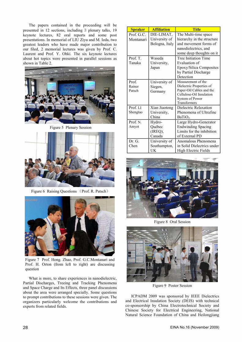
EINA No.16 (November 2009) 28
The papers contained in the proceeding will be
presented in 12 sections, including 3 plenary talks, 19 keynote lectures, 82 oral reports and some post
presentations. In memorial of LIU Ziyu and M. Ieda, two
greatest leaders who have made major contribution to
our filed, 2 memorial lectures was given by Prof. C.
Laurent and Prof. Y. Ohki. The six keynote lectures
about hot topics were presented in parallel sessions as
shown in Table 2.
Figure 5 Plenary Session
Figure 6 Raising Questions (Prof. R. Patsch)
Figure 7 Prof. Hong. Zhao, Prof. G.C.Montanari and
Prof. H. Orton (from left to right) are discussing
question
What is more, to share experiences in nanodielectric,
Partial Discharges, Treeing and Tracking Phenomena
and Space Charge and Its Effects, three panel discussions
about the area were arranged specially. Some questions
to prompt contributions to these sessions were given. The
organizers particularly welcome the contributions and
experts from related fields.
Figure 8 Oral Session
Figure 9 Poster Session
ICPADM 2009 was sponsored by IEEE Dielectrics
and Electrical Insulation Society (DEIS) with technical
co-sponsorship by China Electrotechnical Society and
Chinese Society for Electrical Engineering, National
Natural Science Foundation of China and Heilongjiang
Speaker Affiliation Title
Prof. G.C.
Montanari
DIE-LIMAT,
University of
Bologna, Italy
The Multi-time space
hierarchy in the structure
and movement forms of
nanodielectrics, and
some deep thoughts on it
Prof. T.
Tanaka
Waseda
University,
Japan
Tree Initiation Time
Evaluation of
Epoxy/Silica Composites
by Partial Discharge
Detection
Prof. Rainer
Patsch
University of
Siegen,
Germany
Measurement of the
Dielectric Properties of
Paper-Oil Cables and the
Cellulose-Oil Insulation
System of Power
Transformers
Prof. LI Shengtao
Xian Jiaotong
University,
China
Dielectric Relaxation
Phenomena of Ultrafine
BaTiO3
Prof. N. Amyot
Hydro-
Québec
(IREQ),
Canada
Large Hydro-Generator
Endwinding Spacing
Limits for the inhibition
of External PD
Dr. G.
Chen
University of
Southampton,
UK
Anomalous Phenomena
in Solid Dielectrics under
High Electric Fields

EINA No.16 (November 2009) 29
Province. The conference gained essential sponsor from
some manufacturers. The half-day technical tour was
included in the conference package as well as two
optional tours. The technical tour included two venues,
the Harbin Embraer Aircraft Plant and the Harbin
Electric Machinery Works.
Figure 10 Prof. R. Patsch and Dr. Ch. Weindl are to
the front of a poster
Figure 11 The technical tour visiting the Harbin
Electric Machinery Works
Figure 12 An evening at the dancing on ice
Figure 13 Cranes hovering over Zhalong
National Nature Reserve
Figure 14 IAC members are in the Closing Banquet
Figure 15 IAC members, ICPADM2009 OC members
and volunteers from HUST are in the Closing Banquet
As the chairman of ICPADM 2009, I really hope that
conference was a beneficial and enjoyable experience for
all participants and you have had a nice stay in Harbin.
Further, I would like to give my most heartfelt thanks to
all delegates from all over the world and the member
societies for the efforts they have given to assist in this
scientifically successful conference.
Prof. Qingquan Lei Chairman of ICPADM 2009
Harbin University of Science and Technology,
China [email protected]

EINA No.16 (November 2009) 30
International Conferences to be held in Asia
ICEE 2010 (International Conference on Electrical Engineering)
Dates: July 11-14, 2010
Venue: Paradise Hotel, Busan, Korea
Chairman: Prof. Seung Jae Lee (Myongji University)
Theme: The Smart & The Green in Electrical
Engineering
Organized by KIEE
Co-organized by IEEJ, CSEE, HKIE
Since 1995 the International Conference on Electrical
Engineering (ICEE) has been a premium forum for
sharing knowledge and experience among the most
innovative electrical engineers worldwide. The
Korean Institute of Electrical Engineers (KIEE) is
proud to announce that the 16th ICEE will be held
from July 11th through 14
th in 2010 at Paradise Hotel
in the beautiful city of Busan, Korea. With the theme
of innovation and Convergence in Electrical
Engineering & Technology, the ICEE 2010 is co-
organized by the Institute of Electrical Engineers of
Japan (IEEJ), Chinese Society for Electrical
Engineering (CSEE), and Hong Kong Institute of
Engineers (HKIE).
It is a great pleasure for the KIEE and co-organizers
IEEJ, CSEE, and HKIE to invite prospective authors
to submit papers to the conference.
Key dates: Abstract Submission: December 31, 2009
Acceptance Notification of Abstract: Feb. 1, 2010
Manuscript Submission: April 1, 2010
Acceptance Notification of Paper: May 1, 2010
Secretariat: Ms. Min Jung Kim (KIEE)
Room 901, Science & Technology Building,
635-4, Yucksam-Dong, Kangnam-Ku, Seoul
135-703 KOREA
Tel:+82-70-8222-3371, Mobile:+82-10-9156-3571
Fax: +82-2-3412-8723
E-mail: [email protected]
URL: http://www.icee2010.com
CMD 2010 (International Conference on Condition Monitoring and Diagnosis)
Dates: September 6-11, 2010
Venue: Shibaura Institute of Technology, Tokyo,
Japan
Chairman:::: Prof. Hitoshi Okubo (Nagoya
University, Japan)
Strategic maintenance and replacement of aged power
equipment are key technologies to keep high
reliability of power transmission and distribution
economically. CMD2010 deals issues on various
aspects of aged, replaced or new power equipment,
such as condition monitoring, insulation diagnosis,
failure phenomena based on electrical, mechanical,
chemical and thermal causes, sensing technology, and
asset management techniques. Thus, CMD2010 will
be a precious chance for you to discuss above topics
with a lot of researchers and engineers gathering from
all around the world. It is sponsored by IEEJ and
technically co-sponsored by IEEE Dielectrics and
Electrical Insulation Society and CIGRE.
The conference venue is located in the Tokyo
Metropolitan area, around 30 minutes train and walk
from Tokyo station. Tokyo is a world well-known city
as the capital of Japan with more than 400 year-
history, and has a lot of interesting places such as
beautiful and historical gardens, new cluster of tall
buildings, centers of unique cultures, and so forth.
You will find new aspects of Tokyo in attending
CMD2010.
Key dates:
Abstract Submission January 31, 2010
Acceptance Notices of Abstract: March 31, 2010
Manuscript Submission May 30, 2010
Secretariat: Dr. Tatsuki Okamoto
C/o Electric Power Engineering Research Laboratory,
Central Research Institute of Electric Power Industry
(CRIEPI)
2-6-1 Nagasaka, Yokosuka, Kanagawa 240-0196,
Japan
Tel: +81-46-856-2121, Fax: +81-46-856-3540
Email: [email protected]
URL: http://www.cmd2010.org/
ACED 2010 (Asian Conference on Electrical Discharge)
Dates: November 7-10, 2010
Venue: Xi’an, China
Chairman: Yan-Ming Li (Xi’an Jiaotong Univ.)
Organized by State Key lab of Electrical Insulation &
Power Equipment, Xi’an Jiaotong Univ.
Co-organized by State Key lab of Power
Transmission Equipment & System Security
and New Technology, Xi’an Jiaotong Univ.
Supported by National Natural Science Foundation
of China (NSFC), Chinese Society of Electrical
Engineering (CSEE), China Electrotechnical

EINA No.16 (November 2009) 31
Society (CES)
Sponsored by China Xian Electric Group (XD),
Northwest China Grid Company Limited,
Shaanxi Electric Power Company
The 15th Asian Conference on Electrical Discharge
(ACED 2010) will be held at Xi’an, China, on
November 7-10, 2010. This is the 15th conference of a
series that had its last venues in Bandung, Indonesia
(2008), Hokkaido, Japan (2006), Shenzhen, China
(2004), Seoul, Korea (2002), Kyoto, Japan (2000),
Bandung, Indonesia (1998), Bangkok, Thailand
(1996), Xi’an, China (1994), Oita, Japan (1993) and
Singapore (1992). The purpose of this conference is
intended to provide a forum for researchers, scientists
and engineers to exchange ideas and discuss recent
progress in properties, phenomena and applications of
electrical discharges. The organizing committee
cordially invites you to participate in the conference.
Key dates: Abstract Submission: March 31, 2010
Acceptance Notification of Abstract: April 15, 2010
Manuscript Submission: June 30, 2010
Secretariat: Prof. Guan-Jun Zhang, Dr Sheng-Chang Ji
School of Electrical Engineering Xi’an Jiaotong
University
28 Xianning West Road, Xi’an, Shaanxi 710049,
China
Tel./Fax: +86-29-82668906 or 82668172
Email: [email protected]
URL: http://www.aced2010.com
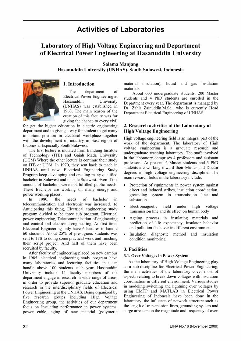
EINA No.16 (November 2009) 32
Activities of Laboratories
Laboratory of High Voltage Engineering and Department
of Electrical Power Engineering at Hasanuddin University
Salama Manjang
Hasanuddin University (UNHAS), South Sulawesi, Indonesia
1. Introduction
The department of
Electrical Power Engineering at
Hasanuddin University
(UNHAS) was established in
1963. The main reason of the
creation of this faculty was for
giving the chance to every civil
for get the higher education in electric engineering
department and to giving a way for student to get many
important position in electrical workplace together
with the development of industry in East region of
Indonesia, Especially South Sulawesi.
The first lecture is mutated from Bandung Institute
of Technology (ITB) and Gajah Mada University
(UGM) Where the other lecture is continue their study
on ITB or UGM. In 1970, they sent back to teach in
UNHAS until now. Electrical Engineering Study
Program keep developing and creating many qualified
bachelor in Sulawesi and outside Sulawesi. Even if the
amount of bachelors were not fulfilled public needs.
These Bachelor are working on many energy and
power working places.
In 1980, the needs of bachelor in
telecommunication and electronic was increased. To
Anticipating this thing, Electrical engineering study
program divided to be three sub program, Electrical
power engineering, Telecommunication of engineering
and control and electronic engineering, At first time,
Electrical Engineering only have 6 lectures to handle
60 students. About 25% of prestigious students was
sent to ITB to doing some practical work and finishing
their script project. And half of them have been
recruited by faculty.
After faculty of engineering placed on new campus
in 1985, electrical engineering study program have
many laboratories and lecturing facilities that can
handle above 100 students each year. Hasanuddin
University include 14 faculty members of the
department engage in research in wide range of areas,
in order to provide superior graduate education and
research in the interdisciplinary fields of Electrical
Power Engineering at the UNHAS. Being organized by
five research groups including High Voltage
Engineering group, the activities of our department
focus on Insulating performance in power systems,
power cable, aging of new material (polymeric
material insulation), liquid and gas insulation
materials.
About 600 undergraduate students, 200 Master
students and 4 PhD students are enrolled in the
Department every year. The department is managed by
Dr. Zahir Zainuddin,M.Sc., who is currently Head
Department Electrical Engineering of UNHAS.
2. Research activities of the Laboratory of
High Voltage Engineering
High voltage engineering field is an integral part of the
work of the department. The laboratory of High
voltage engineering is a graduate research and
undergraduate teaching laboratory. The staff involved
in the laboratory comprises 4 professors and assistant
professors. At present, 6 Master students and 3 PhD
students are working toward their Master and Doctor
degrees in high voltage engineering discipline. The
main research fields in the laboratory include:
• Protection of equipments in power system against
direct and induced strikes, insulation coordination,
grounding system in transmission line and
substation
• Electromagnetic field under high voltage
transmission line and its effect on human body
• Ageing process in insulating materials and
prediction of life expectancy, insulator behavior
and pollution flashover in different environment.
• Insulation diagnostic method and insulation
condition monitoring.
3. Facilities
3.1. Over Voltages in Power System
As the laboratory of High Voltage Engineering play
as a sub-discipline for Electrical Power Engineering,
the main activities of the laboratory cover most of
aspects relating to break down voltages with insulation
coordination in different environment. Various studies
in modeling switching and lightning over voltages by
using EMTP and MATLAB in Electrical Power
Engineering of Indonesia have been done in the
laboratory, the influence of network structure such as
the length of transmission lines, grounding system and
surge arresters on the magnitude and frequency of over

EINA No.16 (November 2009) 33
Figure 1: Power System Simulator NE 9171
voltages is also considered. The modeling results could
be verified in physical simulation by using Power
System Simulator (PSS- NE 9171). The simulator
allows simulating most of cases in switching over
voltages with different structure of the power network.
3.2. Dielectric behavior of insulation under high
stress
Two high voltage testing transformers of 2kVA
with rectifiers provide AC and DC voltages up to
100kV in order to study potential distribution along a
set of insulator and the corona effect in over head lines.
The field distribution within bulk material and along
surface insulators has been modelized by using finite
element method (FEM). These activities allow
understanding the mechanism of pollution flashover in
polluted areas in order to develop remedies method for
such areas. Moreover, physical properties of liquid
dielectrics can be characterized by other facilities
available in the laboratory such as liquid breakdown
testing kit, viscosity meter kit and flash-point
measuring kit.
Figure 2. Simulation of Voltage Distribution on the
Surfaces of Suspension Insulator With Voltage
Stress 70 kV by FEM
3.3. Study Of Insulators Pollution Intensity at
150kV
Analysis of Pollution Intensity need the calculations
performed, it was obtained that ESDD and NSDD values
of pollutant in Jeneponto substation were 0.0782 mg/cm2
and 0.6905 mg/cm2, respectively. From Table 5, it was
obtained that the ESDD value was 0.0728 mg/cm2,
pollution level of Jeneponto substation insulator,
according to its saline content, falls into moderate
contamination level (between 0.06 – 0.1 mg/cm2). When
viewed from NSDD value of 0.6905 mg/cm2, the
pollution level of Jeneponto substation insulator
according to its insoluble pollutant content, can be
categorized as fairly high.
From the average measurement value, a relationship
graphic was made between voltage and leakage current in
insulator.
For both of test insulators show in figure 3, the
maximum average value of leakage current was obtained
in wet polluted test condition (by spraying of Jeneponto
substation), that is 1.33 mA.
Figure 3. Relationship between voltage and leakage
current of insulator (a) dry-clean (b) wet-clean (c)
dry polluted (d) wet polluted
3.4. The Radial Distribution of Temperature in
XLPE Cable an Analysis the Finite Element
Numerical Method
Information at Figure 4 explaining that temperature
distribution cable of XLPE which presented in colour
variation . Visible that distribution temperature not
flattened from centre to external shares. At boundary
condition 305oK ( Figure 4), highest temperature there
are at conductor (colour of orange), while temper-
ature of lower there are ground ( blue colour). As
which seen at Figure 4, for the giving of current 640 A,
highest temperature which yielded at conductor equal
to 342.9849 oK ( 69.9849
oC) and temperature of lower
equal to 305 oK. This matter is caused by the existence
of influence to passed to boundary condition is ground
temperature equal to 305oK and conductor Cu is the
source of heat. Current boundary able to be given only
until 800 A at boundary condition 305 0K,
If have exceeded current boundary of cable of
XLPE have not earn to be justified technically because
Figure 4. Contour distribution cable temperature
of XLPE at 640A all layer with ground tempera- ture 305
0K.
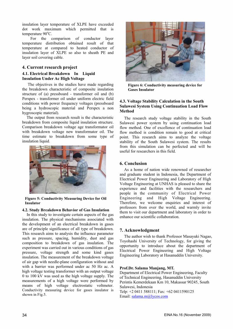
EINA No.16 (November 2009) 34
insulation layer temperature of XLPE have exceeded
dot work maximum which permitted that is
temperature 90oC.
For the comparison of conductor layer
temperature distribution obtained result of that
temperature at compared to heated conductor of
insulation layer of XLPE so also to sheath PE and
layer soil covering cable.
4. Current research project
4.1. Electrical Breakdown In Liquid
Insulation Under Ac High Voltage
The objectives in the studies have made regarding
the breakdown characteristic of composite insulation
structure of (a) pressboard - transformer oil and (b)
Perspex - transformer oil under uniform electric field
conditions with power frequency voltages (pressboard
being a hydroscopic material and Perspex a non
hygroscopic material).
The output from research result is the characteristic
breakdown from composite liquid insulation structure.
Comparison breakdown voltage age transformator oil
with breakdown voltage new transformator oil. The
time estimate to breakdown from some type of
insulation liquid.
Figure 5: Conductivity Measuring Device for Oil
Insulator
4.2. Study Breakdown Behavior of Gas Insulation In this study to investigate certain aspects of the gas
insulation. The physical mechanisms associated with
the development of an electrical breakdown in gases
are of principle significance of all type of breakdown.
This research aims to analysis the influence parameter
such as pressure, spacing, humidity, dust and gas
composition to breakdown of gas insulation. The
experiment was carried out in various conditions of gas
pressure, voltage strength and some kind gases
insulation. The measurement of the breakdown voltage
of air gap with needle-plane configuration without and
with a barrier was performed under ac 50 Hz ac. A
high voltage testing transformer with an output voltage
0 to 100 kV was used as the high voltage supply. The
measurements of a high voltage were performed by
means of high voltage electrostatic voltmeter. Conductivity measuring device for gases insulator is
shown in Fig.5.
Figure 6: Conductivity measuring device for
Gases Insulator
4.3. Voltage Stability Calculation in the South
Sulawesi System Using Continuation Load Flow
Method
The research study voltage stability in the South
Sulawesi power system by using continuation load
flow method. One of excellence of continuation load
flow method is condition remain to good at critical
point. This research aims to analyze the voltage
stability of the South Sulawesi system. The results
from this simulation can be perfected and will be
useful for researchers in this field.
6. Conclusion
As a home of nation wide renowned of researcher
and graduate student in Indonesia, the Department of
Electrical Power Engineering and Laboratory of High
Voltage Engineering at UNHAS is pleased to share the
experience and facilities with the researchers and
people in the community of Electrical Power
Engineering and High Voltage Engineering.
Therefore, we welcome enquiries and interest of
professors from over the world, and warmly invite
them to visit our department and laboratory in order to
enhance our scientific collaboration.
7. Acknowledgment
The author wish to thank Professor Masayuki Nagao,
Toyohashi University of Technology, for giving the
opportunity to introduce about the department of
Electrical Power Engineering and High Voltage
Engineering Laboratory at Hasanuddin University.
Prof.Dr. Salama Manjang, MT. Department of Electrical Power Engineering, Faculty
of Technical Engineering, Hasanuddin University
Perintis Kemerdekaan Km 10, Makassar 90245, South
Sulawesi, Indonesia
Telp: +2 0411 588111; Fax: +62 0411590125
Email: [email protected]
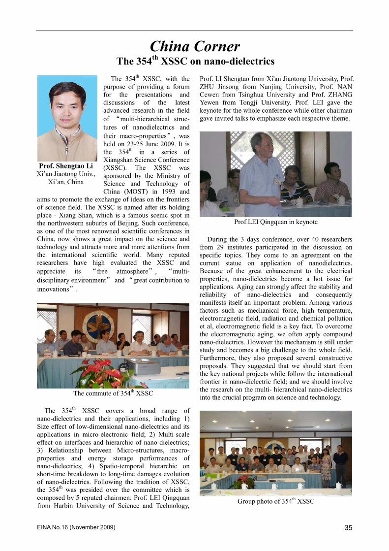
EINA No.16 (November 2009) 35
China Corner The 354
th XSSC on nano-dielectrics
The 354th XSSC, with the
purpose of providing a forum
for the presentations and
discussions of the latest
advanced research in the field
of “multi-hierarchical struc-
tures of nanodielectrics and
their macro-properties”, was
held on 23-25 June 2009. It is
the 354th in a series of
Xiangshan Science Conference
(XSSC). The XSSC was
sponsored by the Ministry of
Science and Technology of
China (MOST) in 1993 and
aims to promote the exchange of ideas on the frontiers
of science field. The XSSC is named after its holding
place - Xiang Shan, which is a famous scenic spot in
the northwestern suburbs of Beijing. Such conference,
as one of the most renowned scientific conferences in
China, now shows a great impact on the science and
technology and attracts more and more attentions from
the international scientific world. Many reputed
researchers have high evaluated the XSSC and
appreciate its “free atmosphere”, “multi-
disciplinary environment” and “great contribution to
innovations”.
The commute of 354
th XSSC
The 354th XSSC covers a broad range of
nano-dielectrics and their applications, including 1)
Size effect of low-dimensional nano-dielectrics and its
applications in micro-electronic field; 2) Multi-scale
effect on interfaces and hierarchic of nano-dielectrics;
3) Relationship between Micro-structures, macro-
properties and energy storage performances of
nano-dielectrics; 4) Spatio-temporal hierarchic on
short-time breakdown to long-time damages evolution
of nano-dielectrics. Following the tradition of XSSC,
the 354th was presided over the committee which is
composed by 5 reputed chairmen: Prof. LEI Qingquan
from Harbin University of Science and Technology,
Prof. LI Shengtao from Xi'an Jiaotong University, Prof.
ZHU Jinsong from Nanjing University, Prof. NAN
Cewen from Tsinghua University and Prof. ZHANG
Yewen from Tongji University. Prof. LEI gave the
keynote for the whole conference while other chairman
gave invited talks to emphasize each respective theme.
Prof.LEI Qingquan in keynote
During the 3 days conference, over 40 researchers
from 29 institutes participated in the discussion on
specific topics. They come to an agreement on the
current statue on application of nanodielectrics.
Because of the great enhancement to the electrical
properties, nano-dielectrics become a hot issue for
applications. Aging can strongly affect the stability and
reliability of nano-dielectrics and consequently
manifests itself an important problem. Among various
factors such as mechanical force, high temperature,
electromagnetic field, radiation and chemical pollution
et al, electromagnetic field is a key fact. To overcome
the electromagnetic aging, we often apply compound
nano-dielectrics. However the mechanism is still under
study and becomes a big challenge to the whole field.
Furthermore, they also proposed several constructive
proposals. They suggested that we should start from
the key national projects while follow the international
frontier in nano-dielectric field; and we should involve
the research on the multi- hierarchical nano-dielectrics
into the crucial program on science and technology.
Group photo of 354
th XSSC
Prof. Shengtao Li Xi’an Jiaotong Univ.,
Xi’an, China
EINA No.16 (November 2009) 36
The 354th XSSC enhance the communication on the
frontiers of nanodielectrics and is sure to bring some
inspirations leading to novel development for
applications.
Appendix 1: Condensed schedule of 345th XSSC
Speakers Department Report Subject
Keynote report:
LEI Qingquan Harbin University of Science
and Technology
The multi-hierarchical structures and movement of
nano-dielectrics
Topic 1: Size effect of low-dimentional nano-dielectrics and its applications in micro-electronic field
ZHU Jinsong Nanjing University Size effects of low-dimentional nano-dielectrics
WANG
Chunlei
Shandong University Simulation of small-scale ferroelectrics physical properties
ZHANG Wei Fudan University High-k and low-k materials in nano integrated circuit
LI Guorong Shanghai Institute of
Ceramics Chinese Academy
of Sciences
Size effect of inorganic, organic and composite dielectrics
Topic 2: Multi-scale effect on interfaces and hierarchic of nano-dielectrics
NAN Cewen Tsinghua University Multi-scale effects of nano-composite dielectrics
HAN Zhichao Institute of Chemistry
Chinese Academy of
Sciences
Some physical and characterization aspects in the multi-Scale
research of multi-Component, multi-phase polymers
LI Jiangyu University of Washington,
American
Electrostatic interaction and depolarization behaved in
nano-dielectric super lattice
ZHU Jianguo Sichuan University Mechanism to enhance the dielectric properties of multi-layer
nano-ferroelectric thin film.
Topic 3: Relationship between Micro-structures, macro-properties and energy storage performances of
nano-dielectrics.
ZHANG
Yewen
Tongji University The micro-structure and space charge behavior of dielectric.
ZHAO Hui Heilongjiang University How one-dimensional nanoelectrodes works in super-capacitor.
JIANG
Yadong
University of Electronic
Science and Technology of
China
Relationship between ultrathin composite membrane structure,
dielectric, piezoelectric properties of organic polymer.
T. Tanaka Waseda University, Japan Nanodielectrics: fundamental and applications.
Topic 4: Spatio-temporal hierarchic on short-time breakdown to long-time damages evolution of
nano-dielectrics
LI Shengtao Xi'an Jiaotong University Evolution from short-time breakdown to long-time damages of
nano-dielectrics.
G. Chen University of Southampton,
UK
Space charge formation and conduction in nanodielectric
materials.
SHI Jing Wuhan University Micro and mesoscopic characterization of electrical ageing on
nano-dielectric.
LI Liang Huazhong University of
Science and Technology
Dielectric behavior of nano-dielectric materials at pulse
high-intensity magnetic field.
Other 12 talks
2009 Lecture Series for Graduate Students
(LSGS 2009) in Xi’an
Lecture Series for Graduate Students (LSGS,
2009), host by State Key Laboratory of Electrical
Insulation and Power Equipment of Xi'an Jiaotong
University, was held from July 25th to August 1
st at
Xi'an, China. Such program is approved by the
Ministry of Education and in a series of “Graduate
Innovative Education Project” which is organized by
the Graduate School of Xi'an Jiaotong University
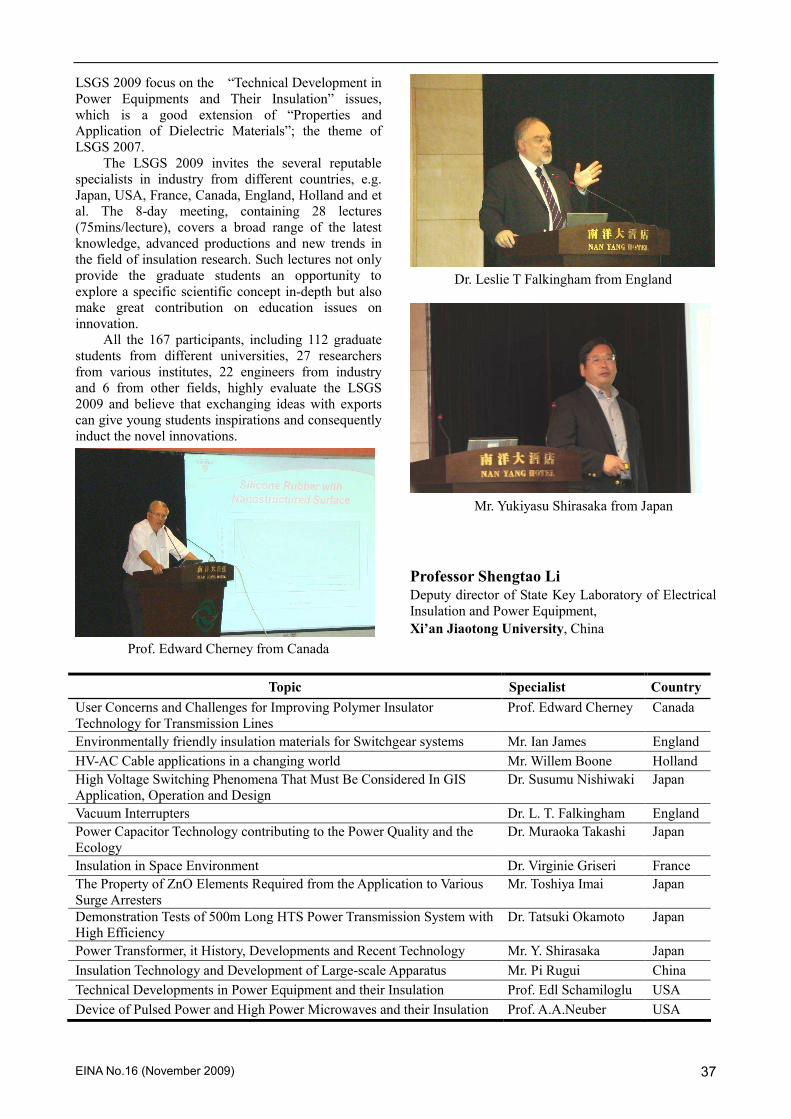
EINA No.16 (November 2009) 37
LSGS 2009 focus on the “Technical Development in
Power Equipments and Their Insulation” issues,
which is a good extension of “Properties and
Application of Dielectric Materials”; the theme of
LSGS 2007.
The LSGS 2009 invites the several reputable
specialists in industry from different countries, e.g.
Japan, USA, France, Canada, England, Holland and et
al. The 8-day meeting, containing 28 lectures
(75mins/lecture), covers a broad range of the latest
knowledge, advanced productions and new trends in
the field of insulation research. Such lectures not only
provide the graduate students an opportunity to
explore a specific scientific concept in-depth but also
make great contribution on education issues on
innovation.
All the 167 participants, including 112 graduate
students from different universities, 27 researchers
from various institutes, 22 engineers from industry
and 6 from other fields, highly evaluate the LSGS
2009 and believe that exchanging ideas with exports
can give young students inspirations and consequently
induct the novel innovations.
Prof. Edward Cherney from Canada
Dr. Leslie T Falkingham from England
Mr. Yukiyasu Shirasaka from Japan
Professor Shengtao Li
Deputy director of State Key Laboratory of Electrical
Insulation and Power Equipment,
Xi’an Jiaotong University, China
Topic Specialist Country
User Concerns and Challenges for Improving Polymer Insulator
Technology for Transmission Lines
Prof. Edward Cherney Canada
Environmentally friendly insulation materials for Switchgear systems Mr. Ian James England
HV-AC Cable applications in a changing world Mr. Willem Boone Holland
High Voltage Switching Phenomena That Must Be Considered In GIS
Application, Operation and Design
Dr. Susumu Nishiwaki Japan
Vacuum Interrupters Dr. L. T. Falkingham England
Power Capacitor Technology contributing to the Power Quality and the
Ecology
Dr. Muraoka Takashi Japan
Insulation in Space Environment Dr. Virginie Griseri France
The Property of ZnO Elements Required from the Application to Various
Surge Arresters
Mr. Toshiya Imai Japan
Demonstration Tests of 500m Long HTS Power Transmission System with
High Efficiency
Dr. Tatsuki Okamoto Japan
Power Transformer, it History, Developments and Recent Technology Mr. Y. Shirasaka Japan
Insulation Technology and Development of Large-scale Apparatus Mr. Pi Rugui China
Technical Developments in Power Equipment and their Insulation Prof. Edl Schamiloglu USA
Device of Pulsed Power and High Power Microwaves and their Insulation Prof. A.A.Neuber USA
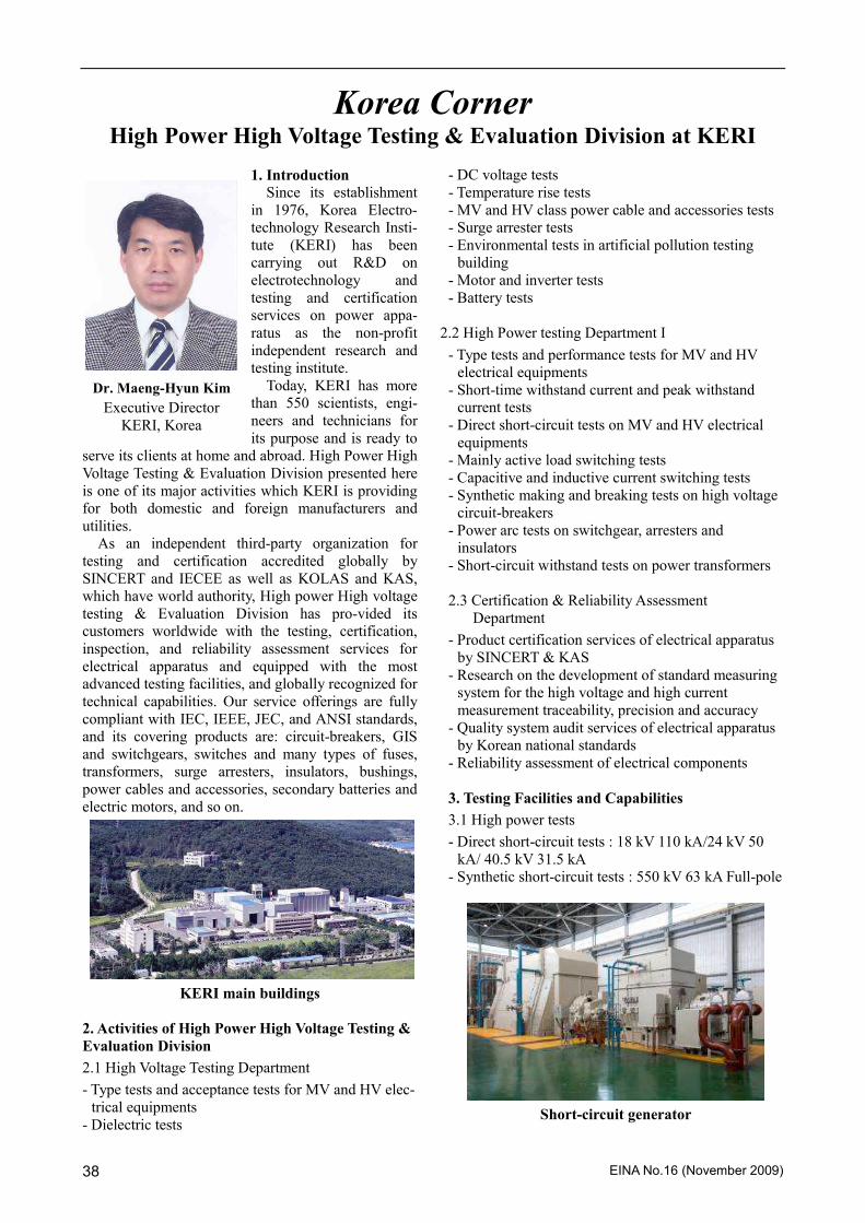
EINA No.16 (November 2009) 38
Korea Corner High Power High Voltage Testing & Evaluation Division at KERI
1. Introduction
Since its establishment
in 1976, Korea Electro-
technology Research Insti-
tute (KERI) has been
carrying out R&D on
electrotechnology and
testing and certification
services on power appa-
ratus as the non-profit
independent research and
testing institute.
Today, KERI has more
than 550 scientists, engi-
neers and technicians for
its purpose and is ready to
serve its clients at home and abroad. High Power High
Voltage Testing & Evaluation Division presented here
is one of its major activities which KERI is providing
for both domestic and foreign manufacturers and
utilities.
As an independent third-party organization for
testing and certification accredited globally by
SINCERT and IECEE as well as KOLAS and KAS,
which have world authority, High power High voltage
testing & Evaluation Division has pro-vided its
customers worldwide with the testing, certification,
inspection, and reliability assessment services for
electrical apparatus and equipped with the most
advanced testing facilities, and globally recognized for
technical capabilities. Our service offerings are fully
compliant with IEC, IEEE, JEC, and ANSI standards,
and its covering products are: circuit-breakers, GIS
and switchgears, switches and many types of fuses,
transformers, surge arresters, insulators, bushings,
power cables and accessories, secondary batteries and
electric motors, and so on.
KERI main buildings
2. Activities of High Power High Voltage Testing &
Evaluation Division
2.1 High Voltage Testing Department
- Type tests and acceptance tests for MV and HV elec-
trical equipments
- Dielectric tests
- DC voltage tests
- Temperature rise tests
- MV and HV class power cable and accessories tests
- Surge arrester tests
- Environmental tests in artificial pollution testing
building
- Motor and inverter tests
- Battery tests
2.2 High Power testing Department I
- Type tests and performance tests for MV and HV
electrical equipments
- Short-time withstand current and peak withstand
current tests
- Direct short-circuit tests on MV and HV electrical
equipments
- Mainly active load switching tests
- Capacitive and inductive current switching tests
- Synthetic making and breaking tests on high voltage
circuit-breakers
- Power arc tests on switchgear, arresters and
insulators
- Short-circuit withstand tests on power transformers
2.3 Certification & Reliability Assessment
Department
- Product certification services of electrical apparatus
by SINCERT & KAS
- Research on the development of standard measuring
system for the high voltage and high current
measurement traceability, precision and accuracy
- Quality system audit services of electrical apparatus
by Korean national standards
- Reliability assessment of electrical components
3. Testing Facilities and Capabilities
3.1 High power tests
- Direct short-circuit tests : 18 kV 110 kA/24 kV 50
kA/ 40.5 kV 31.5 kA
- Synthetic short-circuit tests : 550 kV 63 kA Full-pole
Short-circuit generator
Dr. Maeng-Hyun Kim
Executive Director
KERI, Korea

EINA No.16 (November 2009) 39
- Load switching tests : 36 kV 1000 A, 362 kV 1000 A
Full-pole
- Short-time withstand tests : 150 kA(3phase), 200
kA(1phase)
- Power arc tests : 18 kV 63 kA
Synthetic testing facilities
3.2 High voltage tests
- Lightning/Switching impulse voltage tests: 4200 kV/
2400kV
- AC withstand voltage tests : 1100 kV 2 A
- PD tests : 1100 kV 60Hz, 30 KHz - 400 kHz
- RIV tests : 1100 kV 60Hz, 10 kHz - 30 MHz
- Temperature Rise tests : 3phase, 10,000 A
- Cable tests : 80 kV 3000 A, 9 Feeders
- Surge Arrester tests : 4×10us 200 kA, 8×20us 60 kA
- DC voltage tests : 400 kV 10 mA
- Electric motor and Inverter tests : 90 V - 720 V(LV),
800 – 7200 V(HV), 2 MW
Impulse and AC voltage testing facilities
Arrester testing facilities
4. Epilogue
KERI now owns a 4000 MVA short-circuit
generator, 550KV 63 KA synthetic short-circuit
current making and breaking testing facilities, 550 kV
synthetic capacitive current testing facilities, 120 kA
short-time current withstand testing facilities as well
as 4.2 MV impulse voltage generator, 1100 kV AC
voltage generator, 300 kV artificial pollution, 200 kA
surge arrester, and power cable testing facilities.
Furthermore, KERI will carry out its responsibility
and role as a globally reputable testing laboratory and
certification body on the basis of an outstanding
infrastructure, technical professionalism, and
transparent and systematic operations.
www.keri.re.kr
Address : 28-1, Seongju-dong, Changwon-si,
Gyeongsangnam-do, 641-120, South Korea
High Voltage Laboratory (E-mail : [email protected])
Tel. : (82)55-280-1601, Fax. : (82) 55-280-1512
High Power Laboratory (E-mail : [email protected])
Tel. : (82) 55-280-1602, Fax. : (82) 55-280-1596
Certification Department (E-mail : [email protected])
Tel. : (82) 55-280-1603, Fax. : (82) 55-280-1167
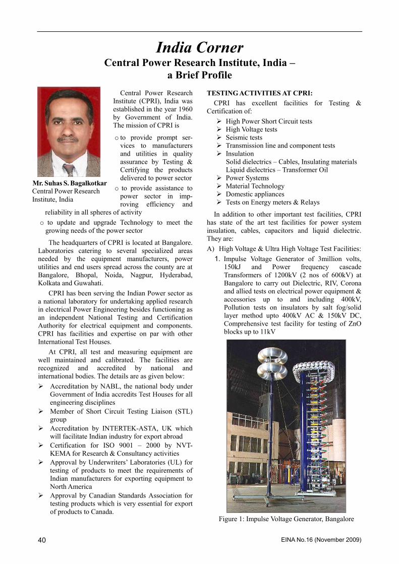
EINA No.16 (November 2009) 40
India Corner Central Power Research Institute, India –
a Brief Profile
Central Power Research
Institute (CPRI), India was
established in the year 1960
by Government of India.
The mission of CPRI is
o to provide prompt ser-
vices to manufacturers
and utilities in quality
assurance by Testing &
Certifying the products
delivered to power sector
o to provide assistance to power sector in imp-
roving efficiency and
reliability in all spheres of activity
o to update and upgrade Technology to meet the
growing needs of the power sector
The headquarters of CPRI is located at Bangalore.
Laboratories catering to several specialized areas
needed by the equipment manufacturers, power
utilities and end users spread across the county are at
Bangalore, Bhopal, Noida, Nagpur, Hyderabad,
Kolkata and Guwahati.
CPRI has been serving the Indian Power sector as
a national laboratory for undertaking applied research
in electrical Power Engineering besides functioning as
an independent National Testing and Certification
Authority for electrical equipment and components.
CPRI has facilities and expertise on par with other
International Test Houses.
At CPRI, all test and measuring equipment are
well maintained and calibrated. The facilities are
recognized and accredited by national and
international bodies. The details are as given below:
� Accreditation by NABL, the national body under
Government of India accredits Test Houses for all
engineering disciplines
� Member of Short Circuit Testing Liaison (STL)
group
� Accreditation by INTERTEK-ASTA, UK which
will facilitate Indian industry for export abroad
� Certification for ISO 9001 – 2000 by NVT-
KEMA for Research & Consultancy activities
� Approval by Underwriters’ Laboratories (UL) for
testing of products to meet the requirements of
Indian manufacturers for exporting equipment to
North America
� Approval by Canadian Standards Association for
testing products which is very essential for export
of products to Canada.
TESTING ACTIVITIES AT CPRI:
CPRI has excellent facilities for Testing &
Certification of:
� High Power Short Circuit tests � High Voltage tests � Seismic tests
� Transmission line and component tests
� Insulation Solid dielectrics – Cables, Insulating materials
Liquid dielectrics – Transformer Oil
� Power Systems
� Material Technology
� Domestic appliances
� Tests on Energy meters & Relays
In addition to other important test facilities, CPRI
has state of the art test facilities for power system
insulation, cables, capacitors and liquid dielectric.
They are:
A) High Voltage & Ultra High Voltage Test Facilities:
1. Impulse Voltage Generator of 3million volts,
150kJ and Power frequency cascade
Transformers of 1200kV (2 nos of 600kV) at
Bangalore to carry out Dielectric, RIV, Corona
and allied tests on electrical power equipment &
accessories up to and including 400kV,
Pollution tests on insulators by salt fog/solid
layer method upto 400kV AC & 150kV DC,
Comprehensive test facility for testing of ZnO
blocks up to 11kV
Figure 1: Impulse Voltage Generator, Bangalore
Mr. Suhas S. Bagalkotkar
Central Power Research
Institute, India
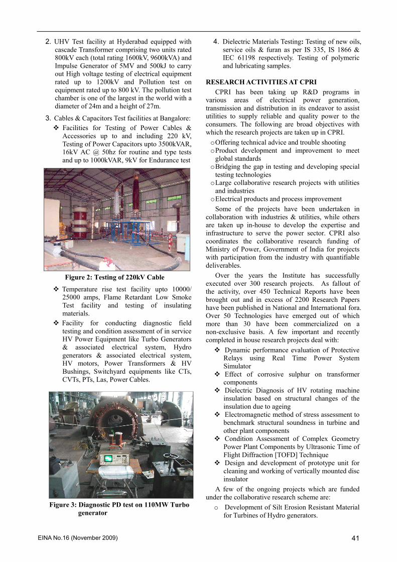
EINA No.16 (November 2009) 41
2. UHV Test facility at Hyderabad equipped with cascade Transformer comprising two units rated
800kV each (total rating 1600kV, 9600kVA) and
Impulse Generator of 5MV and 500kJ to carry
out High voltage testing of electrical equipment
rated up to 1200kV and Pollution test on
equipment rated up to 800 kV. The pollution test
chamber is one of the largest in the world with a
diameter of 24m and a height of 27m.
3. Cables & Capacitors Test facilities at Bangalore:
� Facilities for Testing of Power Cables &
Accessories up to and including 220 kV,
Testing of Power Capacitors upto 3500kVAR,
16kV AC @ 50hz for routine and type tests
and up to 1000kVAR, 9kV for Endurance test
Figure 2: Testing of 220kV Cable
� Temperature rise test facility upto 10000/
25000 amps, Flame Retardant Low Smoke
Test facility and testing of insulating
materials.
� Facility for conducting diagnostic field
testing and condition assessment of in service
HV Power Equipment like Turbo Generators
& associated electrical system, Hydro
generators & associated electrical system,
HV motors, Power Transformers & HV
Bushings, Switchyard equipments like CTs,
CVTs, PTs, Las, Power Cables.
4. Dielectric Materials Testing: Testing of new oils,
service oils & furan as per IS 335, IS 1866 &
IEC 61198 respectively. Testing of polymeric
and lubricating samples.
RESEARCH ACTIVITIES AT CPRI
CPRI has been taking up R&D programs in
various areas of electrical power generation,
transmission and distribution in its endeavor to assist
utilities to supply reliable and quality power to the
consumers. The following are broad objectives with
which the research projects are taken up in CPRI.
o Offering technical advice and trouble shooting o Product development and improvement to meet
global standards
o Bridging the gap in testing and developing special testing technologies
o Large collaborative research projects with utilities and industries
o Electrical products and process improvement
Some of the projects have been undertaken in
collaboration with industries & utilities, while others
are taken up in-house to develop the expertise and
infrastructure to serve the power sector. CPRI also
coordinates the collaborative research funding of
Ministry of Power, Government of India for projects
with participation from the industry with quantifiable
deliverables.
Over the years the Institute has successfully
executed over 300 research projects. As fallout of
the activity, over 450 Technical Reports have been
brought out and in excess of 2200 Research Papers
have been published in National and International fora.
Over 50 Technologies have emerged out of which
more than 30 have been commercialized on a
non-exclusive basis. A few important and recently
completed in house research projects deal with:
� Dynamic performance evaluation of Protective
Relays using Real Time Power System
Simulator
� Effect of corrosive sulphur on transformer
components
� Dielectric Diagnosis of HV rotating machine
insulation based on structural changes of the
insulation due to ageing
� Electromagnetic method of stress assessment to
benchmark structural soundness in turbine and
other plant components
� Condition Assessment of Complex Geometry
Power Plant Components by Ultrasonic Time of
Flight Diffraction [TOFD] Technique
� Design and development of prototype unit for
cleaning and working of vertically mounted disc
insulator
A few of the ongoing projects which are funded
under the collaborative research scheme are:
o Development of Silt Erosion Resistant Material
for Turbines of Hydro generators.
Figure 3: Diagnostic PD test on 110MW Turbo
generator

EINA No.16 (November 2009) 42
o National Effort to develop Technology for
Custom Power Devices – Development of (a) 4
x 500 kVAr STATCOM for IT-Park, and 2.5
MVAr STATCOM for Steel Plant.
o Development of High Temperature
Superconducting Transformers
o Development of a prototype of 132kV Optical
Current Transformer for use in the 132kV
system
RESEARCH ON COMPOSITE INSULATORS
CPRI has established expertise in the area of
development and testing of composite insulators and
have developed compound for silicone rubber
insulator. Prototype of the first Indigenous composite
insulator of 400 kV class has been developed under
the ages of Department of scientific and industrial
research for a manufacturer in Hyderabad, India.
CPRI has recently carried out systematic long-term
(1000 hour under salt fog) ageing studies on
composite insulators with bio contamination deposit
on its surface in the form of algae observed in cold
countries especially on silicone rubber insulators.
When fungi and other microorganisms colonize the
surface of an insulator, they are suspected to impede
the drying of the insulator surface and accelerate the
insulator surface degradation by enzymes secreted by
fungal contaminants. The study results are being
analyzed to understand the process and to determine
the effect on the insulator dielectric strength.
Figure 4: Virgin insulator (on the left) and two
Insulators with bio contamination
DIELECTRIC TESTING OF UHV INSULATION
The Ultra high voltage laboratory at Hyderabad is
an out door laboratory established more than 15 years
ago with a vision that India shall have to adopt 1200
kV ac and ± 800 kV dc class transmission systems in
future. This has materialized and Indian Utilities, in
particular Power Grid Corporation of India, are in the
process of establishing them. In this endeavor, CPRI is
playing a key role by way of carrying out dielectric
tests on insulator strings and substation equipment
insulation.
The lab has so far tested a large number of 765 kV
ac transmission system insulator strings of various
configurations, circuit breaker, CVT, CT and bus post
insulators for their required insulation levels.
800 kV dc transmission system class insulators
have been tested for Lightning impulse withstand of
2250 kVp and switching impulse withstand of 1850
kVp.
The laboratory carried out an important study to
optimize the conductor - tower air insulation clearance
for adoption in Indian 1200 kV ac transmission line
and corona studies to optimize the conductor
configuration for 1200 kV transmission lines.
Figure 5: Testing under progress to optimize tower
window clearance of 1200 kV ac line
Figure 6: Corona cage with bundle conductor
strung inside.
ACKNOWLEDGEMENT This article is prepared with inputs from Dr. R.S.
Shivakumara Aradhya ([email protected]), Mr. B.
Gunasekaran ([email protected]) and Dr. N.
Vasudev ([email protected])
Mr. Suhas S. Bagalkotkar Joint Director / Assistant Public Information Officer
Marketing Publicity & Planning Division
Central Power Research Institute,
Bangalore, India Tel.: +91 - 80 - 2360 2329
Email : [email protected]
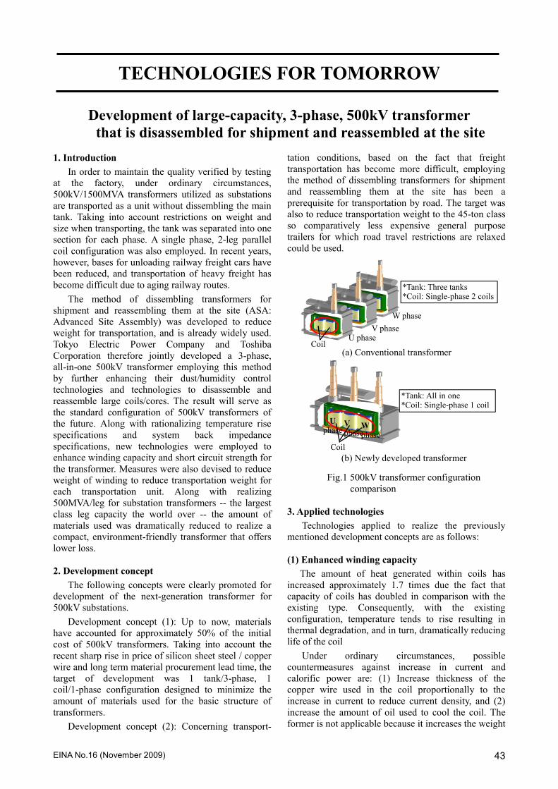
EINA No.16 (November 2009) 43
TECHNOLOGIES FOR TOMORROW
Development of large-capacity, 3-phase, 500kV transformer
that is disassembled for shipment and reassembled at the site
1. Introduction
In order to maintain the quality verified by testing
at the factory, under ordinary circumstances,
500kV/1500MVA transformers utilized as substations
are transported as a unit without dissembling the main
tank. Taking into account restrictions on weight and
size when transporting, the tank was separated into one
section for each phase. A single phase, 2-leg parallel
coil configuration was also employed. In recent years,
however, bases for unloading railway freight cars have
been reduced, and transportation of heavy freight has
become difficult due to aging railway routes.
The method of dissembling transformers for
shipment and reassembling them at the site (ASA:
Advanced Site Assembly) was developed to reduce
weight for transportation, and is already widely used.
Tokyo Electric Power Company and Toshiba
Corporation therefore jointly developed a 3-phase,
all-in-one 500kV transformer employing this method
by further enhancing their dust/humidity control
technologies and technologies to disassemble and
reassemble large coils/cores. The result will serve as
the standard configuration of 500kV transformers of
the future. Along with rationalizing temperature rise
specifications and system back impedance
specifications, new technologies were employed to
enhance winding capacity and short circuit strength for
the transformer. Measures were also devised to reduce
weight of winding to reduce transportation weight for
each transportation unit. Along with realizing
500MVA/leg for substation transformers -- the largest
class leg capacity the world over -- the amount of
materials used was dramatically reduced to realize a
compact, environment-friendly transformer that offers
lower loss.
2. Development concept
The following concepts were clearly promoted for
development of the next-generation transformer for
500kV substations.
Development concept (1): Up to now, materials
have accounted for approximately 50% of the initial
cost of 500kV transformers. Taking into account the
recent sharp rise in price of silicon sheet steel / copper
wire and long term material procurement lead time, the
target of development was 1 tank/3-phase, 1
coil/1-phase configuration designed to minimize the
amount of materials used for the basic structure of
transformers.
Development concept (2): Concerning transport-
tation conditions, based on the fact that freight
transportation has become more difficult, employing
the method of dissembling transformers for shipment
and reassembling them at the site has been a
prerequisite for transportation by road. The target was
also to reduce transportation weight to the 45-ton class
so comparatively less expensive general purpose
trailers for which road travel restrictions are relaxed
could be used.
Fig.1 500kV transformer configuration
comparison
3. Applied technologies
Technologies applied to realize the previously
mentioned development concepts are as follows:
(1) Enhanced winding capacity
The amount of heat generated within coils has
increased approximately 1.7 times due the fact that
capacity of coils has doubled in comparison with the
existing type. Consequently, with the existing
configuration, temperature tends to rise resulting in
thermal degradation, and in turn, dramatically reducing
life of the coil
Under ordinary circumstances, possible
countermeasures against increase in current and
calorific power are: (1) Increase thickness of the
copper wire used in the coil proportionally to the
increase in current to reduce current density, and (2)
increase the amount of oil used to cool the coil. The
former is not applicable because it increases the weight
*Tank: Three tanks *Coil: Single-phase 2 coils
(a) Conventional transformer
U phase V phase
W phase
Coil
Coil
U phase
V phase
W phase
(b) Newly developed transformer
*Tank: All in one *Coil: Single-phase 1 coil

EINA No.16 (November 2009) 44
of the coil so a general purpose trailer cannot be used
for transport. In the case of the latter, it is not
preferable to increase the amount of oil in order to
secure reliability in relation to the phenomenon of
static electrification caused by friction produced by oil
flowing between insulation (charge build-up due to
static electrification increases proportional to 2 or 3
times the velocity of the oil flow).
The winding was therefore significantly improved
by streamlining specifications and applying new
technologies while holding down increase in oil flow
and copper wire size as follows:
a) Development of coils that can be used at high
temperatures
As the result of determining insulation and life
characteristics of thermal upgraded paper, it was
decided to use amine added insulation paper to wrap
around the copper wire of coils because it resists
thermal degradation and offers the required insulation
performance while wrapping the copper wire. This
raised the temperature rise limit of the coil 10K higher
than the JEC standard value.
b) Suppression of heat generated from the coil
Continuous Transposed Cable (CTC) arranged
from fine wire is used for the copper wire of the coil.
Heat generation (eddy-current loss) caused by
intersection of leakage flux is suppressed by
minimizing the height and width of the wire
(eddy-current loss ∝ the square of wire width).
Fig. 2: Technologies applied to coils (copper
wire / insulating paper)
c) Establishment of 3D magnetic field analysis
technology
Because leakage flux produced from the coil
increases as current per coil increases, heat generation
and local overheating tend to occur when leakage flux
intersects with the tank/core. Along with getting a
detailed understanding of temperature of various parts
utilizing 3D magnetic field analysis technology to
effectively cope with increasing leakage flux, a new
magnetic shield has been developed to effectively
suppress local overheating.
(2) Improvement of mechanical strength
If leg capacity of the coil is doubled, magnetic
mechanical force applied on the coil increases
approximately 1.6 times that of a conventional coil,
Fig. 3: Magnetic field analysis model and local
overheating analysis examples
and coil deformation tends to occur. As was previously
stated, in order to reduce weight, strength cannot be
enhanced by using thicker copper wire. Mechanical
strength has therefore been dramatically improved by
utilizing the following technologies:
a) Formulation of dynamic analysis technologies for
coil deformation
Mechanical strength of inside winding used to be
evaluated by static evaluation of conductor buckling
strength between two points of support (forced
buckling), but analysis of dynamic free buckling
thinking of the winding considering that a loop was
conducted. Precision of winding strength evaluation
was improved this time by conducting model tests and
dynamic analysis of free buckling of winding to which
the test results are applied. Based on this, system
impedance that in the past could not be incorporated
into evaluation of short circuit mechanical strength as
the margin of analytical error was successfully added
to the specifications.
b) Application of high strength wire
High strength wire with 20% improved strength
processed by applying pressure to copper wire has
been applied in some parts.
(3) Improvement/rationalization of ASA
Transformers
A reliable method of dissembling transformers for
shipment and reassembling them at the site (ASA) was
established by designing jigs/tools to reduce weight for
transport and developing dust/humidity control
technologies for large transformers.
a) Development of jigs/tools to reduce
transportation weight
It was also decided to switch from iron to
aluminum tanks used for transporting coils in order to
reduce weight. Combined with the previously
mentioned coil weight reduction technologies,
transportation weight was reduced to the 45-ton level.
*Copper wire: CTC (configured of fine wire)
*Insulating paper: Amine addedinsulation paper (Thermal upgraded paper)
Coil
Iron core
Tank
Temperature of various parts
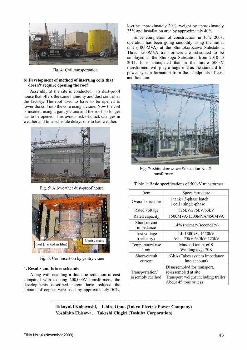
EINA No.16 (November 2009) 45
Fig. 4: Coil transportation
b) Development of method of inserting coils that
doesn't require opening the roof
Assembly at the site is conducted in a dust-proof
house that offers the same humidity and dust control as
the factory. The roof used to have to be opened to
lower the coil into the core using a crane. Now the coil
is inserted using a gantry crane and the roof no longer
has to be opened. This avoids risk of quick changes in
weather and time schedule delays due to bad weather.
Fig. 5: All-weather dust-proof house
Fig. 6: Coil insertion by gantry crane
4. Results and future schedule
Along with enabling a dramatic reduction in cost
compared with existing 500,000V transformers, the
developments described herein have reduced the
amount of copper wire used by approximately 50%,
loss by approximately 20%, weight by approximately
35% and installation area by approximately 40%.
Since completion of construction in June 2008,
operation has been going smoothly using the initial
unit (1000MVA) at the Shintokorozawa Substation.
Three 1500MVA transformers are scheduled to be
employed at the Shinkoga Substation from 2010 to
2011. It is anticipated that in the future 500kV
transformers will play a huge role as the standard for
power system formation from the standpoints of cost
and function.
Fig. 7: Shintokorozawa Substation No. 2
transformer
Table 1: Basic specifications of 500kV transformer
Gantry crane Coil (Packed in film)
Item Specs./structure
Overall structure 1 tank / 3-phase batch
1 coil / single-phase
Rated voltage 525kV/275kV/63kV
Rated capacity 1500MVA/1500MVA/450MVA
Short-circuit
impedance 14% (primary/secondary)
Test voltage
(primary)
LI: 1300kV, 1550kV
AC: 475kV-635kV-475kV
Temperature rise
limit
Max. oil temp: 60K Winding avg: 70K
Short-circuit
current
63kA (Takes system impedance
into account)
Transportation/
assembly method
Disassembled for transport,
re-assembled at site
Transport weight including trailer:
About 45 tons or less
-------------------------------------------------------------------------------------------------
Takayuki Kobayashi, Ichiro Ohno (Tokyo Electric Power Company)
Yoshihito Ebisawa, Takeshi Chigiri (Toshiba Corporation)
EINA No.16 (November 2009) 46
The Largest Scale Dielectric Tests
of 1100kV Gas Circuit Breaker
1. Introduction
UHV AC 1100kV transmission is an effective
transmission technology for large-capacity,
long-distance transmission. Development of 1100kV
equipment began in the latter half of 1980’s by Tokyo
Electric Power Company (TEPCO) in Japan. TEPCO
has been performing field verification tests of 1100kV
equipment since 1996 at test substation [1-2]. In
China, the AC 1100kV transmission tests were started
from 2008. The dielectric type tests were carried out
on 1100kV Gas Circuit Breaker (GCB) for China. The
voltages of these tests were the world highest level.
Moreover, there was a combined voltage test which
applies the power-frequency voltage (AC voltage) to
both terminals across the open switching device. This
test item which was not in the test specification of
1100kV GCB for Japan was added. In this paper, the
AC-AC combined voltage test method and result are
reported.
2. Structure of 1100kV GCB
For the 1100kV GCB, the resistor insertion method
was applied for both closing and opening operation to
suppress the switching overvoltage level. Structure of
1100kV GCB is shown in Fig. 1-2. The 1100kV GCB
consists of two main interrupters and two resistor
interrupters with resistor units in parallel. Between
switching device terminals of two main interrupters,
grading capacitors are installed in parallel respectively
in order to divide a voltage with two interrupters
equally. As two interrupters are arranged
symmetrically, there is no difference in structure
found from the each connection terminal side of
1100kV GCB.
3 Test Method
In the dielectric type tests of 1100kV GCB for
China, there was a combined voltage test which
applies the power-frequency voltage (AC voltage) to
both terminals across the open switching device for 1
minute. The AC-AC combined test voltages are
635kVrms for one terminal and 1100kVrms for the other
terminal at reversed phase.
There are three difficult problems to perform the
AC-AC combined voltage test at reversed phase.
1. Two AC voltage sources are needed for the
AC-AC combined voltage test. But, generally
a high-voltage testing laboratory has only one
large scale of testing transformer in a testing
room.
2. Since 1100kV GCB with two breaks has
grading capacitors across terminals, a large
current flows through the capacitors in the test
circuit. One source voltage also influences on
the other source voltage greatly due to the
capacitors. For this reason, it is very difficult
to control the applied voltages individually.
3. A large power supply is needed due to the
current through the grading capacitors of
1100kV GCB.
These problems have been solved by the following
methods.
1. A testing transformer of rated voltage 2300kV
has already been installed in a testing room.
Another testing transformer of rated voltage
900kV was transferred into the same testing
room as the other AC voltage source. The
AC-AC combined voltage test setup is shown
in Fig. 3.
2. The AC-AC combined voltage test was able to
be carried out with the following circuit
composition. One AC voltage source circuit
capacitor
resistor
Fig. 2. Block diagram of 1100kV GCB
Fig. 1. Schematic diagram of 1100kV GCB
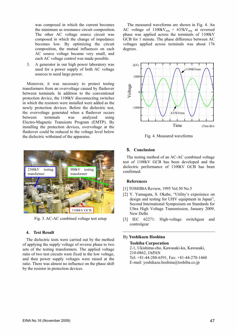
EINA No.16 (November 2009) 47
was composed in which the current becomes
the minimum as resonance circuit composition.
The other AC voltage source circuit was
composed in which the change of impedance
becomes low. By optimizing the circuit
composition, the mutual influences on each
AC source voltage became very small, and
each AC voltage control was made possible.
3. A generator in our high power laboratory was
used for a power supply of both AC voltage
sources to need large power.
Moreover, it was necessary to protect testing
transformers from an overvoltage caused by flashover
between terminals. In addition to the conventional
protection device, the 1100kV disconnecting switches
in which the resistors were installed were added as the
newly protection devices. Before the dielectric test,
the overvoltage generated when a flashover occurs
between terminals was analyzed using
Electro-Magnetic Transients Program (EMTP). By
installing the protection devices, overvoltage at the
flashover could be reduced to the voltage level below
the dielectric withstand of the apparatus.
4. Test Result
The dielectric tests were carried out by the method
of applying the supply voltage of reverse phase to two
sets of the testing transformers. The applied voltage
ratio of two test circuits were fixed in the low voltage,
and then power supply voltages were raised at the
ratio. There was almost no influence on the phase shift
by the resistor in protection devices.
The measured waveforms are shown in Fig. 4. An
AC voltage of 1100kVrms + 635kVrms at reversed
phase was applied across the terminals of 1100kV
GCB for 1 minute. The phase difference between AC
voltages applied across terminals was about 176
degrees.
5. Conclusion
The testing method of an AC-AC combined voltage
test of 1100kV GCB has been developed and the
dielectric performance of 1100kV GCB has been
confirmed.
References
[1] TOSHIBA Review, 1995 Vol.50 No.5
[2] Y. Yamagata, S. Okabe, “Utility’s experience on
design and testing for UHV equipment in Japan”,
Second International Symposium on Standards for
Ultra High Voltage Transmission, January 2009,
New Delhi
[3] IEC 62271: High-voltage switchgear and
controlgear
By Yoshikazu Hoshina
Toshiba Corporation 2-1, Ukishima-cho, Kawasaki-ku, Kawasaki,
210-0862, JAPAN
Tel: +81-44-288-6591, Fax: +81-44-270-1460
E-mail: [email protected]
TimeVoltage
(kV)
(5ms/div)
1100kVrms
635kVrms
-1000
0
1000
Fig. 4. Measured waveforms
2300kV testing
transformer
900kV testing
transformer
UHV GCB
Fig. 3. AC-AC combined voltage test setup
1100kV GCB

EINA No.16 (November 2009) 48
TECHNOLOGIES ALERT
Electrostatic Potential Distribution Measurement in Vacuum
Surface charging affects the surface breakdown
on insulation materials in a vacuum. To investigate
this effect, Hitachi, Ltd. developed an electrostatic
potential distribution measurement system. The
potential distribution is measured by an electrostatic
voltmeter probe that is scanned along the sample
surface in a vacuum without a contact between the
sample and the probe. This system was used to
measure the potential distributions of two test
samples (Sample A and B) and to investigate the
correlation between the roughness of the insulation
Electrostatic
Voltmeter
ProbeSample
Vacuum Chamber
HVPS
Glass Vessel
Ground
electrode
Sample
Lead wire
30 mm
5 mm
Probe
HV
electrode
Lead wire
Schematic diagram of electrostatic potential
distribution measurement system and
overview of samples
material and the surface charge. Sample A was
borosilicate glass with a flat surface, and Sample B
was sandblasted borosilicate glass. The measured
potential distribution profile of Sample A had an
area with a high electric field near the HV electrode,
and the maximum field was 700 V/mm. On the
other hand, the profile of Sample B was close to
linear, and the maximum electric field was 420
V/mm. The roughness of the surface can reduce the
amount of surface charging. The effect of changing
the roughness of the surface and the results of the
discharge tests will be clarified.
-10
-8
-6
-4
-2
0Potential (kV)
Position (10mm/div.)
Sample A
Sample B
Ground
Electrode
HV electrode
700 V/mm
420 V/mm
Electric potential distributions of Sample A and B
By Hiroshi Morita
Hitachi, Ltd. / Hitachi Research Laboratory
1-1, Omika-cho 7-chome, Hitachi-shi, Ibaraki-ken,
319-1292 Japan
http://www.hitachi.com/
E-mail:[email protected]
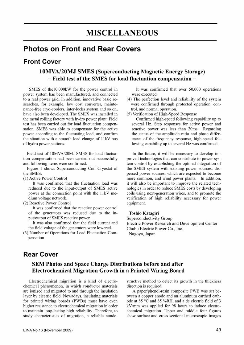
EINA No.16 (November 2009) 49
MISCELLANEOUS
Photos on Front and Rear Covers
Front Cover
10MVA/20MJ SMES (Superconducting Magnetic Energy Storage)
−−−− Field test of the SMES for load fluctuation compensation −−−−
SMES of the10,000kW for the power control in
power system has been manufactured, and connected
to a real power grid. In addition, innovative basic re-
searches, for example, low cost converter, mainte-
nance-free cryo-coolers, inter-locks system and so on,
have also been developed. The SMES was installed in
the metal rolling factory with hydro power plant. Field
test has been carried out for load fluctuation compen-
sation. SMES was able to compensate for the active
power according to the fluctuating load, and confirm
the situation with a smooth load change of 11kV bus
of hydro power stations.
Field test of 10MVA/20MJ SMES for load fluctua-
tion compensation had been carried out successfully
and following items were confirmed.
Figure 1 shows Superconducting Coil Cryostat of
the SMES.
(1) Active Power Control
It was confirmed that the fluctuation load was
reduced due to the input/output of SMES active
power at the connection point with the 11kV me-
dium voltage network.
(2) Reactive Power Control
It was confirmed that the reactive power control
of the generators was reduced due to the in-
put/output of SMES reactive power.
It was also confirmed that the field current and
the field voltage of the generators were lowered.
(3) Number of Operations for Load Fluctuation Com-
pensation
It was confirmed that over 50,000 operations
were executed.
(4) The perfection level and reliability of the system
were confirmed through protected operation, con-
trol, and normal operation.
(5) Verification of High-Speed Response
Confirmed high-speed following capability up to
several Hz. Step responses for active power and
reactive power was less than 20ms. Regarding
the status of the amplitude ratio and phase differ-
ences of the frequency response, high-speed fol-
lowing capability up to several Hz was confirmed.
In the future, it will be necessary to develop im-
proved technologies that can contribute to power sys-
tem control by establishing the optimal integration of
the SMES system with existing power sources, dis-
persed power sources, which are expected to become
more common, and wind power plants. In addition,
it will also be important to improve the related tech-
nologies in order to reduce SMES costs by developing
coils using next-generation wires, and to promote the
verification of high reliability necessary for power
equipment.
Toshio Katagiri
Superconductivity Group
Electric Power Research and Development Center
Chubu Electric Power Co., Inc.
Nagoya, Japan
Rear Cover
SEM Photos and Space Charge Distributions before and after
Electrochemical Migration Growth in a Printed Wiring Board
Electrochemical migration is a kind of electro-
chemical phenomenon, in which conductor materials
are ionized and migrated to and through the insulation
layer by electric field. Nowadays, insulating materials
for printed wiring boards (PWBs) must have even
higher resistance to electrochemical migration in order
to maintain long-lasting high reliability. Therefore, to
study characteristics of migration, a reliable nonde-
structive method to detect its growth in the thickness
direction is required.
A paper/phenol-resin composite PWB was set be-
tween a copper anode and an aluminum earthed cath-
ode at 85 °C and 85 %RH, and a dc electric field of 3
kV/mm was applied for 98 hours to induce electro-
chemical migration. Upper and middle four figures
show surface and cross sectional microscopic images
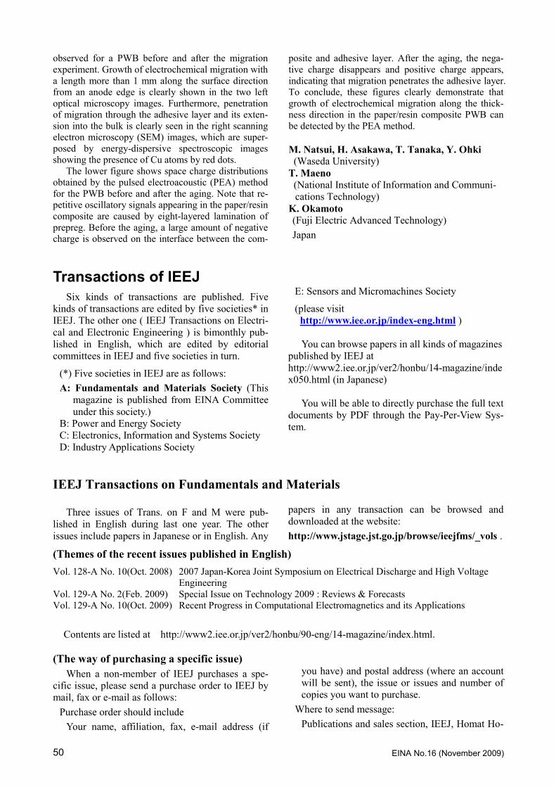
EINA No.16 (November 2009) 50
observed for a PWB before and after the migration
experiment. Growth of electrochemical migration with
a length more than 1 mm along the surface direction
from an anode edge is clearly shown in the two left
optical microscopy images. Furthermore, penetration
of migration through the adhesive layer and its exten-
sion into the bulk is clearly seen in the right scanning
electron microscopy (SEM) images, which are super-
posed by energy-dispersive spectroscopic images
showing the presence of Cu atoms by red dots.
The lower figure shows space charge distributions
obtained by the pulsed electroacoustic (PEA) method
for the PWB before and after the aging. Note that re-
petitive oscillatory signals appearing in the paper/resin
composite are caused by eight-layered lamination of
prepreg. Before the aging, a large amount of negative
charge is observed on the interface between the com-
posite and adhesive layer. After the aging, the nega-
tive charge disappears and positive charge appears,
indicating that migration penetrates the adhesive layer.
To conclude, these figures clearly demonstrate that
growth of electrochemical migration along the thick-
ness direction in the paper/resin composite PWB can
be detected by the PEA method.
M. Natsui, H. Asakawa, T. Tanaka, Y. Ohki
(Waseda University)
T. Maeno
(National Institute of Information and Communi-
cations Technology)
K. Okamoto
(Fuji Electric Advanced Technology)
Japan
Transactions of IEEJ
Six kinds of transactions are published. Five
kinds of transactions are edited by five societies* in
IEEJ. The other one ( IEEJ Transactions on Electri-
cal and Electronic Engineering ) is bimonthly pub-
lished in English, which are edited by editorial
committees in IEEJ and five societies in turn.
(*) Five societies in IEEJ are as follows:
A: Fundamentals and Materials Society (This
magazine is published from EINA Committee
under this society.)
B: Power and Energy Society
C: Electronics, Information and Systems Society
D: Industry Applications Society
E: Sensors and Micromachines Society
(please visit
http://www.iee.or.jp/index-eng.html )
You can browse papers in all kinds of magazines
published by IEEJ at
http://www2.iee.or.jp/ver2/honbu/14-magazine/inde
x050.html (in Japanese)
You will be able to directly purchase the full text
documents by PDF through the Pay-Per-View Sys-
tem.
IEEJ Transactions on Fundamentals and Materials
Three issues of Trans. on F and M were pub-
lished in English during last one year. The other
issues include papers in Japanese or in English. Any
papers in any transaction can be browsed and
downloaded at the website:
http://www.jstage.jst.go.jp/browse/ieejfms/_vols .
(Themes of the recent issues published in English)
Vol. 128-A No. 10(Oct. 2008) 2007 Japan-Korea Joint Symposium on Electrical Discharge and High Voltage
Engineering
Vol. 129-A No. 2(Feb. 2009) Special Issue on Technology 2009 : Reviews & Forecasts
Vol. 129-A No. 10(Oct. 2009) Recent Progress in Computational Electromagnetics and its Applications
Contents are listed at http://www2.iee.or.jp/ver2/honbu/90-eng/14-magazine/index.html.
(The way of purchasing a specific issue)
When a non-member of IEEJ purchases a spe-
cific issue, please send a purchase order to IEEJ by
mail, fax or e-mail as follows:
Purchase order should include
Your name, affiliation, fax, e-mail address (if
you have) and postal address (where an account
will be sent), the issue or issues and number of
copies you want to purchase.
Where to send message:
Publications and sales section, IEEJ, Homat Ho-
EINA No.16 (November 2009) 51
rizon Bldg.8fl.,
6-2 Gobancho, Chiyoda-ku, Tokyo 102-0076,
Japan
Fax: +81-3-3221-3704
E-mail: [email protected]
Please visit:
http://www2.iee.or.jp/ver2/honbu/13-publication
/index030.html(in Jaspanese)
You can browse papers in all kinds of magazines
published by IEEJ at
http://www2.iee.or.jp/ver2/honbu/14-magazine/i
ndex050.html (in Japanese)
You will be able to directly purchase the full text
documents by PDF through the Pay-Per-View Sys-
tem.
IEEJ TEEE (Transactions on Electrical and Electronic Engineering)
The journal “IEEJ TEEE was launched in May 2006. It is an online magazine and published bimonthly
from John Wiley & Sons, Inc. on the website:
http://www3.interscience.wiley.com/cgi-bin/jhome/112638268
This magazine is covered in Scientific Science Citation IndexTM
Expanded by Thomson Reuters.
IEEJ Technical Reports
Technical reports listed below were prepared by investigation committees in technical committees A to E
in IEEJ and published form September in 2008 to September in 2009. Their extended summaries can be read
in English on the web site below but the text of technical reports are described in Japanese..
No. Title Pub.date Price 1127 Failure Extension Prevention Technology by Frequency Relay System 2008/09 ¥1,260
1128 The latest Technology of Adaptive Motion Control to Environment 2008/09 ¥6,142
1129 Advanced computational techniques for practical electromagnetic field analysis(2008.9.10) 2008/09 ¥5,512
1130 The Statistics of Setting and Operation Situation of Shunt Power Capacitor in Japan 2008/09 ¥3,465
1131 Current Situations and Problems of LSI Design and Education 2008/09 ¥4,252
1132 Power Technology of Japan through the Experience of Developments and Applications of Surge
Arresters for AC3.3 - 1100kV and HVDC125 - 600kV Power Systems
2008/09 ¥2,625
1133 The Present State and View about Harmonic Magnetic Applications 2008/09 ¥3,465
1134 Wavelet and Knowledge Discovery Technology 2008/09 ¥4,095
1135 Education and Training Structure of Power System Operator 2008/10 ¥1,470
1136 Technology Trend of Application of Environmentally Friendly Materials to Electrical Equipments 2008/10 ¥3,465
1137 New Control Technology for Nano-scale Servo 2008/10 ¥6,300
1138 Advanced Energy Utilization MHD Power Generation 2008/11 ¥4,252
1139 Reduction Technology of Iron Loss in Stator Core of Synchronous Generator 2008/11 ¥3,937
1140 Systematize technology of multi degrees of freedom motors 2008/11 ¥4,410
1141 Risk Management Technologies for Nuclear Power 2008/12 ¥2,992
1142 Technical Report on "Advanced Measurements and Simulations for Discharges and Electrical Insu-
lation in Vacuum"
2008/12 ¥4,725
1143 Studies on Environmental Impact Reduction in Automobile Traffic with ITS Technologies 2009/01 ¥4,095
1144 Study on equipment troubles of hydroelectric power plants 2009/01 ¥5,197
1145 Trend in the latest technologies and applications of permanent magnet synchronous motors 2009/01 ¥4,095
1146 The Structural Technology of ICT-oriented Central Supervisory Control System 2009/02 ¥3,465
1147 Lightning striking characteristics to structures 2009/03 ¥4,252
1148 Characteristics Evaluation and Potential Applications of Polymer Nanocomposites as Evolutional
Electrical Insulating Materials
2009/03 ¥5,040
1149 Thermal Stability, Applications and Coercivity of High-Performance Permanent Magnets
- Evaluation of Long Term Stability of Rare Earth Magnets in a Partially Magnetized State and In-
vestigation on their Applications and Coercivity of the Magnets -
2009/03 ¥3,622
1150 The present simulation technologies and its applications 2009/06 ¥4,095
1151 Advances and industrial applications of soft computing 2009/04 ¥6,930
1152 Current Status of Development of Flywheel Energy Storage Systems using Superconducting Mag-
netic Bearings
2009/04 ¥4,252
1153 Electromagnetic Fields of Nanometer Electromagnetic Waves and X-ray
- New Frontiers of Electromagnetic Wave Engineering -
2009/04 ¥4,252
1154 Elemental technology use for industrial linear electromagnetic drive systems and their trend 2009/05 ¥3,937
1155 Technology Trends in Energy Systems of Information Apparatuses in Homes and Offices in the
Broadband Network Age
2009/06 ¥4,095
1156 Trend of Fusion Technology on Electric and Mechanical Systems for Magnetic Suspension Applica-
tions
2009/06 ¥3,780
EINA No.16 (November 2009) 52
1157 Laser micro/nano scale processing for fundamental research and industrial applications 2009/06 ¥4,095
1158 Bioinstrumentation technology in the medical and welfare field 2009/06 ¥4,095 1159 Industrial Applications of Pulsed Power Technologies 2009/07 ¥3,307
1160 Infrared Technology for Safety and Security 2009/07 ¥3,937
1161 Current and Future Technical trends on Energy Storage Application Technologies for Mobile Vehi-
cles
2009/07 ¥4,410
1162 Advanced metal sputtering plasmas and their recent trends 2009/07 ¥3,780
1163 Steel Corrosion and Wear Phenomena of Overhead Transmission Lines 2009/07 ¥3,570
1164 The Trends and Study of Life-cycle Managements for Distribution Equipment 2009/07 ¥5,197
1165 Energy Saving Technology and Application Trends at Industrial Fields 2009/07 ¥4,252
1166 Hydrogen and Fuel Cells in Future Energy Networks 2009/08 ¥4,252 1167 The review of the human health effect due to the exposure to electromagnetic fields 2009/08 ¥4,095
1168 Electromagnetic Field Analysis for Rotating Machine Design and Performance Evaluation 2009/08 ¥4,410
1169 New Generation Electric and Magnetic Actuators 2009/09 ¥3,780
1170 A Report on Industrial Applications of High Power Semiconductor LDs 2009/09
Abstract of the technical report can be browsed on the web site:
http://www.iee.or.jp/index-eng.html ---> “Publications”
or http://www2.iee.or.jp/ver2/honbu/90-eng/13-publication/index.html
Application for Membership of IEEJ
A member of IEEJ receives a monthly journal
(The Journal of The Institute of Electrical Engineers
of Japan) and one transaction out of five (A: Fun-
damentals and Materials in which the activity of
DEI is included, B: Power and Energy, C: Elec-
tronics, Information and System, D: Industry Ap-
plications, E: Sensors). The journal gives inter-
esting readings about the latest science and tech-
nology in the field of Power Energy, Power Appa-
ratus, Electronics, Information Engineering, Mate-
rials and so on. The transaction gives review pa-
pers, research papers, letters and other information.
Total fee for joining IEEJ as a general individual
membership is ¥ 12,400 which consists of initiation
fee ¥ 1,200, annual membership fee ¥ 10,000 and
overseas postage of journal ¥ 1,200 (¥ : Japanese
Yen).
You can choose web application or sending an
application form by e-mail or airmail for your ap-
plication.
Please visit http://www2.iee.or.jp/ver2/
honbu/90-eng/12-bid/index.html
Way for Purchasing Proceedings of IEEJ Technical Meetings and IEEJ Technical Reports
(1) Proceedings of Symposia
You can request it to the business and service
section of IEEJ. ([email protected])
(2) Proceedings of Technical Meetings
You can purchase them by subscription for a
year (Jan. to Dec.). Please request it to the
business and service section of IEEJ.
(3) Technical reports
You can order technical reports from the pub-
lishing section of IEEJ. ([email protected])
Please visit: http://www.bookpark.ne.jp/cm/ieej/search.asp?flag=
0&category=%8BZ%8Fp%95%F1%8D%90&mode
or
https://www.iee.or.jp/cfml/OA/front/NonAuthenticat
e/bookpur/fbo_BookList.cfm?Kubun=5
Price ¥: Japanese Yen
(with tax, without postage)

EINA No.16 (November 2009) 53
Postal and e-mail Address of IEEJ:
The Institute of Electrical Engineers of Japan
8F HOMAT HORIZON Bldg., 6-2, Goban-cho, Chiyoda-ku, Tokyo 102-0076, Japan
(General affairs Section)
E-mail: [email protected]
(Business Service Section)
E-mail: [email protected]
(Publication & Sales Section)
E-mail: [email protected]
Fax: +81-3-3221-3704 (common)
EINA No.16 (November 2009) 54
Members of EINA Committee in 2009
Masayuki Nagao Toyohashi University of Technology (Chairman)
Toshikatsu Tanaka Waseda University (Adviser)
Yoshiyuki Inoue Toshiba Corporation (Secretary)
Masahiro Kozako Kyushu Institute of Technology (Secretary)
Hiroya Homma Central Research Institute of Electric Power Industry (Task Force)
Kazuyuki Tohyama Numazu National College of Technology (Task Force)
Naohumi Chiwata Hitachi Cable, Ltd.
Osamu Fujii NGK Insulators, Ltd.
Toshinari Hashizume Yazaki Electric Wire Co., Ltd.
Noriyuki Hayashi Kyushu University
Kunihiko Hidaka The University of Tokyo
Masayuki Hirose Sumitomo Electric Industries, Ltd.
Satoru Hishikawa Huntsman Advanced Materials K. K.
Hiromasa Honjo Mitsubishi Cable Industries Ltd.
Satoru Itabashi Nissin Electric Co., Ltd.
Mitsumasa Iwamoto Tokyo Institute of Technology
Jumpei Kusukawa Hitachi, Ltd.
Kouji Miyahara Chubu Electric Power Co., Inc.
Shinichi Mukoyama Furukawa Electric Co., Ltd.
Hirotaka Muto Mitsubishi Electric Corporation
Hiroyuki Nishikawa Shibaura Institute of Technology
Yoshimichi Ohki Waseda University
Kenji Okamoto Fuji Electric Advanced Technology Co., Ltd.
Minoru Okashita Showa Cable System Co., Ltd.
Yasuo Suzuoki Nagoya University
Tatsuo Takada Tokyo City University
Tohru Takahashi VISCAS Corporation
Shin-ichi Tsuchiya Tokyo Electric Power Company
Yasuo Umeda Kansai Electric Power Co., Inc.
Hisanao Yamashita Keio University
Motoshige Yumoto Tokyo City University
Web Site for EINA Magazine
You can see the EINA magazine including back numbers at http://eina.ws/
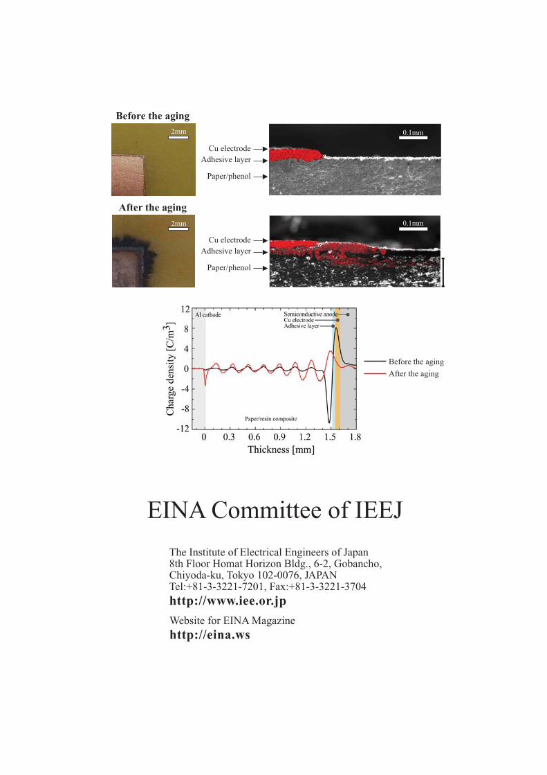
Website for EINA Magazine
http://eina.ws
EINA Committee of IEEJ
Before the aging
After the aging
Cu electrode
Adhesive layer
Paper/phenol
Cu electrode
Adhesive layer
Paper/phenol
Before the aging
After the aging
0.1mm2mm
2mm 0.1mm