noise characterization of a cmos x-ray image sensor
TRANSCRIPT

Noise Characterization of a CMOS
X-Ray Image Sensor
by
Yi Jie Liang
A thesis
presented to the University of Waterloo
in fulfillment of the
thesis requirement for the degree of
Master of Applied Science
in
Electrical and Computer Engineering
Waterloo, Ontario, Canada, 2018
c© Yi Jie Liang 2018
I hereby declare that I am the sole author of this thesis. This is a true copy of the thesis,
including any required final revisions, as accepted by my examiners.
I understand that my thesis may be made electronically available to the public.
ii
Abstract
The objective of this thesis is to validate the noise performance of a high resolution
CMOS X-ray imager. We carry out a detailed noise analysis on a four-quadrant CMOS
imager and the external hardware. Careful analysis reveals several design issues on the
printed circuit board (PCB). We propose solutions to improve the PCB design. Experimen-
tal results show the modified system outperforms the original one with a sizable margin.
iii

Acknowledgements
Pursuing a MASc. is an adventure, and this journey would not have been as fulfilling
and rewarding without the guidance and the support of many people.
First, I would like to express profound gratitude to my supervisor, Professor Karim S
Karim and Professor Peter Levine for their invaluable support, supervision and technical
guidance throughout my graduate study at University of Waterloo. Professor Karim al-
ways inspire me to achieve a higher goal and give me new preservatives on difficult research
topics. His moral support kept me motivated and enabled me to complete my work suc-
cessfully. Professor Levine not only gives very detailed suggestions on my research work
but also continuously supervises the project at the finest standard. It has been my great
pleasure to work with Professor karim and Professor Levine.
Second, much of the work would not be possible without the help, discussion and
cooperation from the following individuals: Hummer Li and Abdallah El-Falou, who always
standby me on our journey rain or shine. Alex Duanmu, who forever reminds me to go to
school everyday, weekend included and provides 24/7 academic support anytime I needed.
Chris Scott, who works with me on this chip to get phase contrast image almost everyday
on campus. Ahmet Camlica, who manages to pursue a PHD degree while becoming a new
parent. And many others in STAR team who supports me throughout this master study.
Last, I would like to thank my parents, Carrie and William for their consistent encour-
agement and unconditional love throughout my time. It is their support that enables me
to pursue new heights of my life. I will forever be grateful and it is my chance to contribute
to family.
v

Table of Contents
List of Tables xi
List of Figures xiii
List of Acronyms xv
1 Introduction 1
1.1 X-ray Physics and Applications . . . . . . . . . . . . . . . . . . . . . . . . 1
1.2 X-ray Imager Technology . . . . . . . . . . . . . . . . . . . . . . . . . . . . 2
1.2.1 Analog and Digital Imaging . . . . . . . . . . . . . . . . . . . . . . 2
1.2.2 X-ray Conversion and Readout Technology . . . . . . . . . . . . . . 3
1.3 Amorphous Selenium/CMOS X-ray Imager . . . . . . . . . . . . . . . . . . 4
1.4 Noise Performance Metric in X-ray Sensor . . . . . . . . . . . . . . . . . . 6
1.5 Thesis Objectives . . . . . . . . . . . . . . . . . . . . . . . . . . . . . . . . 8
1.6 Thesis Outline . . . . . . . . . . . . . . . . . . . . . . . . . . . . . . . . . . 9
vii

2 Review of Noise in CMOS Imagers 11
2.1 Fixed-Pattern Noise and Temporal Noise . . . . . . . . . . . . . . . . . . . 11
2.1.1 Thermal Noise . . . . . . . . . . . . . . . . . . . . . . . . . . . . . 12
2.1.2 Shot Noise . . . . . . . . . . . . . . . . . . . . . . . . . . . . . . . . 13
2.1.3 Flicker Noise . . . . . . . . . . . . . . . . . . . . . . . . . . . . . . 14
2.2 Noise Analysis in Linear Circuits . . . . . . . . . . . . . . . . . . . . . . . 16
3 Active Pixel Sensor Noise Analysis 21
3.1 3T and 4T APS Operation Overview . . . . . . . . . . . . . . . . . . . . . 21
3.2 3T APS noise analysis . . . . . . . . . . . . . . . . . . . . . . . . . . . . . 25
3.2.1 3T APS Phase 1 (Reset) . . . . . . . . . . . . . . . . . . . . . . . . 25
3.2.2 3T APS Phase 2 (Integration) . . . . . . . . . . . . . . . . . . . . . 27
3.2.3 3T APS Phase 3 (Sampling) . . . . . . . . . . . . . . . . . . . . . . 28
3.2.4 3T APS Summary . . . . . . . . . . . . . . . . . . . . . . . . . . . 30
3.2.5 4T APS Structure and Operation . . . . . . . . . . . . . . . . . . . 31
3.3 4T APS noise analysis . . . . . . . . . . . . . . . . . . . . . . . . . . . . . 33
3.3.1 4T APS Phase 1 (Reset) . . . . . . . . . . . . . . . . . . . . . . . . 33
3.3.2 4T APS Phase 2 (Integration) . . . . . . . . . . . . . . . . . . . . . 35
3.3.3 4T APS Phase 3 (Sampling) . . . . . . . . . . . . . . . . . . . . . . 36
3.3.4 4T APS Summary . . . . . . . . . . . . . . . . . . . . . . . . . . . 37
3.4 Summary . . . . . . . . . . . . . . . . . . . . . . . . . . . . . . . . . . . . 38
viii

4 Simulation and Measured Result Comparison 39
4.1 Details of the Device under Test . . . . . . . . . . . . . . . . . . . . . . . . 39
4.2 Leakage Measurement . . . . . . . . . . . . . . . . . . . . . . . . . . . . . 42
4.3 Signal Path Measurement . . . . . . . . . . . . . . . . . . . . . . . . . . . 47
4.4 Normal Operation Measurement . . . . . . . . . . . . . . . . . . . . . . . . 49
4.4.1 Operation Parameters Setup . . . . . . . . . . . . . . . . . . . . . . 49
4.4.2 Quadrant 1 Measurement . . . . . . . . . . . . . . . . . . . . . . . 51
4.4.3 Quadrant 2 and 3 Measurement . . . . . . . . . . . . . . . . . . . 55
4.4.4 Quadrant 4 Measurement . . . . . . . . . . . . . . . . . . . . . . . 57
4.4.5 Noise Measurement Summary . . . . . . . . . . . . . . . . . . . . . 58
4.5 Correlated Double Sampling . . . . . . . . . . . . . . . . . . . . . . . . . . 60
4.6 Summary . . . . . . . . . . . . . . . . . . . . . . . . . . . . . . . . . . . . 64
5 PCB Design Review 65
5.1 ADC Layout . . . . . . . . . . . . . . . . . . . . . . . . . . . . . . . . . . . 65
5.2 Component Selection . . . . . . . . . . . . . . . . . . . . . . . . . . . . . . 71
5.3 Grounding Scheme . . . . . . . . . . . . . . . . . . . . . . . . . . . . . . . 73
5.4 Board Modification Result Comparison . . . . . . . . . . . . . . . . . . . 75
6 Conclusion and Future Work 79
References 81
ix


List of Tables
4.1 Pixel Node Capacitance of Different Quadrants . . . . . . . . . . . . . . . 41
4.2 Leakage Current during Integration. . . . . . . . . . . . . . . . . . . . . . . 46
4.3 Noise Measurement and Breakdown for 4 Quadrants . . . . . . . . . . . . 59
4.4 Output Referred SNR Calculation . . . . . . . . . . . . . . . . . . . . . . . 62
xi


List of Figures
1.1 Side and Top View of the Imager . . . . . . . . . . . . . . . . . . . . . . . 5
1.2 Block Diagram and Physical Layout of the Imager . . . . . . . . . . . . . . 6
1.3 X-ray Imaging System Signal Path . . . . . . . . . . . . . . . . . . . . . . 7
1.4 X-ray images with different SNR values. . . . . . . . . . . . . . . . . . . . 7
2.1 Circuit Models of Thermal Noise Source . . . . . . . . . . . . . . . . . . . 12
2.2 Thermal Noise Single-sided PSD . . . . . . . . . . . . . . . . . . . . . . . . 13
2.3 Transistor Models of Flicker Noise Source . . . . . . . . . . . . . . . . . . . 15
2.4 Integrator Circuit. . . . . . . . . . . . . . . . . . . . . . . . . . . . . . . . 17
2.5 RC Circuit. . . . . . . . . . . . . . . . . . . . . . . . . . . . . . . . . . . . 18
2.6 Signal Path with Multiple Noise Sources . . . . . . . . . . . . . . . . . . . 19
3.1 Simplified 3T APS Circuit Model . . . . . . . . . . . . . . . . . . . . . . . 22
3.2 3T Pixel Timing Diagram . . . . . . . . . . . . . . . . . . . . . . . . . . . 24
3.3 3T Pixel Circuit Model during Reset Phase. . . . . . . . . . . . . . . . . . 26
xiii
3.4 Simplified 4T APS Circuit Model . . . . . . . . . . . . . . . . . . . . . . . 31
3.5 4T Pixel Timing Diagram . . . . . . . . . . . . . . . . . . . . . . . . . . . 32
3.6 Circuit Model during Transfer Gate Turns Off. . . . . . . . . . . . . . . . . 33
3.7 Leakage Current in 4T APS Circuit . . . . . . . . . . . . . . . . . . . . . . 35
4.1 Pixel Schematic Screen Captures in Cadence . . . . . . . . . . . . . . . . . 40
4.2 Pixel Schematic Screen Captures in Cadence . . . . . . . . . . . . . . . . 41
4.3 Quadrant 1 Leakage Current Measurements . . . . . . . . . . . . . . . . . 43
4.4 Quadrant 1 Noise Behavior vs Various Reset Voltages . . . . . . . . . . . . 44
4.5 Quadrant 1 Voltage Drop due to Charge Injection vs Various Reset Voltages 45
4.6 Quadrant 2 Noise Behavior at Various Integration Time . . . . . . . . . . . 46
4.7 Noise Value on Signal Path In DN with Various Reset Voltage . . . . . . . 48
4.8 Quadrant 1 Sample Reset Measurement vs Simulation . . . . . . . . . . . . 52
4.9 Quadrant 1 Sample Read Measurement vs Simulation . . . . . . . . . . . . 54
4.10 Quadrant 2 Measurement vs Simulation . . . . . . . . . . . . . . . . . . . . 55
4.11 Quadrant 3 Measurement vs Simulation . . . . . . . . . . . . . . . . . . . . 56
4.12 Quadrant 4 Measurement vs Simulation . . . . . . . . . . . . . . . . . . . . 58
4.13 CDS Measurement with Various Integration Time and Reset Level . . . . . 61
4.14 Sample and Hold Circuit for CDS Operation . . . . . . . . . . . . . . . . . 62
5.1 ADC Noise PSD from Battery . . . . . . . . . . . . . . . . . . . . . . . . . 66
xiv
5.2 ADC Output from Ramping Signal . . . . . . . . . . . . . . . . . . . . . . 67
5.3 Histogram of Last 5 bits of ADC Output . . . . . . . . . . . . . . . . . . . 68
5.4 ADC Layout Issues . . . . . . . . . . . . . . . . . . . . . . . . . . . . . . . 69
5.5 Oscilloscope Screen Shot Comparison with Clock Signal Disable during Con-
version . . . . . . . . . . . . . . . . . . . . . . . . . . . . . . . . . . . . . . 70
5.6 Quadrant 3 Noise Value with AVDD Reduction . . . . . . . . . . . . . . . 72
5.7 Single-Point Ground System Illustration . . . . . . . . . . . . . . . . . . . 74
5.8 Ground Plane Mistake Illustration . . . . . . . . . . . . . . . . . . . . . . . 75
5.9 Samples of Decoupling Capacitors . . . . . . . . . . . . . . . . . . . . . . . 76
5.10 Test Results Comparison for Modifications . . . . . . . . . . . . . . . . . . 77
xv


Chapter 1
Introduction
1.1 X-ray Physics and Applications
Since first discovered in 1895, X-rays have played an important role in many scientific
and medical applications. Thanks to the short wavelength (between 0.01 and 100 nm),
X-ray photons are able to pass through some materials while visible light photons cannot.
The energy of X-rays is usually measured in kilo electron volts (keV), which is equal to
approximately 1.6× 10⁻¹⁶ J [1]. Also, X-rays can be categorized into two groups based on
their energy. X-ray photons with energy less than 3 keV are referred to as “soft” because
they are easily absorbed by water and air. X-rays with energies more than 3 keV are
referred to as “hard”. By controlling the photon energy level, X-ray photons can penetrate
materials of various densities [2].
X-ray imaging is a popular method for non-destructive testing (NDT) and biomedical
imaging. In NDT, dense objects within a specimen can be observed without damaging
1
the specimen’s external structure. Therefore, X-ray is extensively employed in aircraft
manufacturing and the fossil fuel industries. X-ray imaging also has a lot of biomedical
applications, such as mammography, which is used for breast cancer diagnosis; computed
tomography, which is generating cross sectional images of body organs; and fluoroscopy,
which is a continuous X-ray imaging on a monitor for diagnostic processes. However, due
to the high energy level of X-ray photons, excessive X-rays exposure can harm living cells.
This interaction brings up the concern about X-ray imaging damage to the human body.
As a result, X-ray exposures with lower dosage are usually preferred to reduce the potential
harm.
1.2 X-ray Imager Technology
1.2.1 Analog and Digital Imaging
Like the old fashioned way of visible light imaging, X-ray can be captured through an
object with a film/screen. The exposed film is placed into a development solution to
convert silver ions into metallic silver [3]. The disadvantage of this method is that data
cannot be validated until the film is developed and reviewed by the radiologists. If any
mistake is made, there is a risk to the patients for exposing to X-ray again.
On the other hand, digital imaging detectors utilize sensors to convert X-ray photons
into electron and hole pairs. By separating the pairs with high voltage bias, the charges
are collected and translated into voltage or current by the pixel circuit to read out. The
electrical information is then translated and stored in digital format. Since post processing
2
is done digitally, it is fast and no dark room or chemical solution is needed. However,
digital X-ray imaging had low resolution and low image quality when the technology was
first introduced. Yet with improvements in both fabrication and design, digital X-ray
imagers are having a rapidly increasing share of the X-ray detector market.
1.2.2 X-ray Conversion and Readout Technology
There are two general methods to convert X-ray photons: indirect and direct conversion.
Indirect conversion uses scintillators to convert X-rays into visible light and then translates
the optical signal into electrical charge with visible-light sensors. Alternatively, direct con-
version employs semiconducting or photoconducting materials to convert the energy from
absorbed X-rays directly into electrical charge signals [4]. One disadvantage of the indirect
conversion method is that light spreads in every direction after hitting the scintillator,
resulting in loss of spatial resolution. Reducing the thickness of scintillator material would
help mitigate light spreading, yet it also reduces the absorption rate of X-ray. After X-ray
photons are converted into electrical charges, the next step is to collect these charges with
the readout circuit. The most commonly used technologies for pixel implementation are
thin film transistor (TFT), charge coupled device (CCD), and complementary metal-oxide-
semiconductor (CMOS). TFT can be fabricated in standard manufacturing facilities with
low cost, but TFT devices also have low mobilities and cannot be made into high resolu-
tion panels due to the size of the transistor. One of the main reasons that CCD sensors
occupy high end applications is that they exhibit superior noise performance compared to
CMOS image sensors [5]. However, CCD readout relies on toggling voltage of each pixel
sequentially to shift the electrical signal to the next adjacent pixel, which not only limits
3

the readout speed, but also causes error propagation. Error propagation happens when one
or more pixels along the readout path has a small percentage error in transferring charges.
A small initial percentage error can lead to very large error in the end as the size of the
sensor increases.
In a CMOS imager, the signal in each pixel can be processed individually without suf-
fering error propagation introduced by shared channel readout. Another great advantage
for CMOS imager is the use of standard CMOS mixed-signal technology. It allows man-
ufacturing imaging devices to be monolithically integrated onto the same piece of silicon
while CCD imager requires numerous chips for the sensor, driver and signal condition-
ing [6]. This reduces the complexity and cost of the system substantially. Also, readout
speed is no longer limited by the sequential readout method. Furthermore, CMOS imager
can also feature on-chip signal processing because an analog-to-digital converter (ADC)
can be integrated on the same chip.
1.3 Amorphous Selenium/CMOS X-ray Imager
In this thesis, we will focus on noise characterization of a direct-conversion CMOS X-
ray imager prototype designed by a former graduate student, Alireza Parsafar [7]. An
amorphous selenium (a-Se) X-ray sensor is integrated onto a CMOS pixel array as shown
in Figure 1.1a. A-Se is the most commonly used protoconducting material, thanks to its
low cost and low dark current property. Moreover, it provides high spatial resolution (on
the order of 5 µm) for X-ray photon energies between 20 and 40 keV [8]. Figure 1.1b
illustrates the imager after a-Se direct deposition.
4
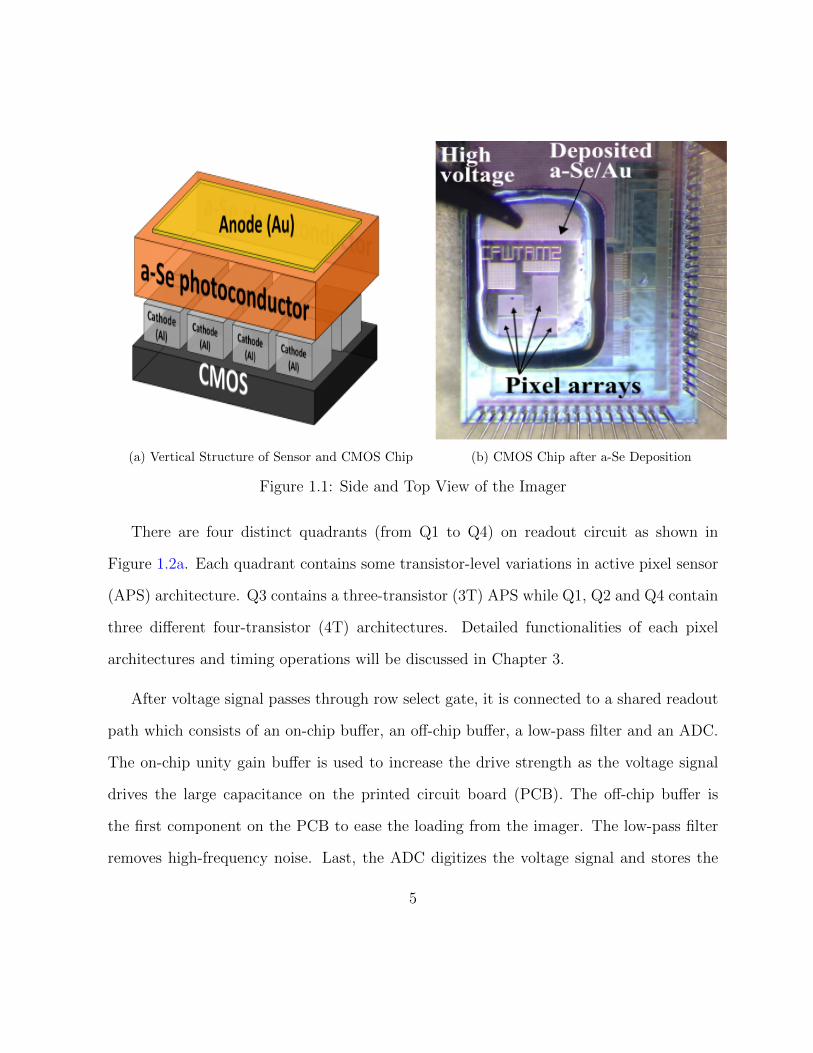
(a) Vertical Structure of Sensor and CMOS Chip (b) CMOS Chip after a-Se Deposition
Figure 1.1: Side and Top View of the Imager
There are four distinct quadrants (from Q1 to Q4) on readout circuit as shown in
Figure 1.2a. Each quadrant contains some transistor-level variations in active pixel sensor
(APS) architecture. Q3 contains a three-transistor (3T) APS while Q1, Q2 and Q4 contain
three different four-transistor (4T) architectures. Detailed functionalities of each pixel
architectures and timing operations will be discussed in Chapter 3.
After voltage signal passes through row select gate, it is connected to a shared readout
path which consists of an on-chip buffer, an off-chip buffer, a low-pass filter and an ADC.
The on-chip unity gain buffer is used to increase the drive strength as the voltage signal
drives the large capacitance on the printed circuit board (PCB). The off-chip buffer is
the first component on the PCB to ease the loading from the imager. The low-pass filter
removes high-frequency noise. Last, the ADC digitizes the voltage signal and stores the
5

(a) Block Diagram of Pixel Array (b) Physical Layout of CMOS Chip
Figure 1.2: Block Diagram and Physical Layout of the Imager
result in a field-programmable gate array (FPGA) for further processing.
1.4 Noise Performance Metric in X-ray Sensor
During the development process of CMOS imagers, noise is considered as one of the most
important distortions that degrade the visual quality. In practical systems, transistor
operating points and capacitance levels are time-varying due to transistor switchings within
pixels. Therefore, careful noise analysis must be performed on each state of pixels in order
to understand the overall noise characteristics. In addition, noise performance is affected
not only by the design and fabrication, but also the operating condition, physical layout
of the system and the overall system signal path as illustrated in Figure 1.3.
6

Figure 1.3: X-ray Imaging System Signal Path
Figure 1.4: X-ray images with different SNR values.
7

The most commonly used image quality metric is signal-to-noise ratio (SNR), defined
as the ratio between useful signal that the imager detects and the noise floor of the imager.
Figure 1.4 illustrates that the quality of an X-ray image is heavily affected by the SNR.
There are two general approaches to improve the image quality. On one hand, we can
increase X-ray flux or the conversion gain of the sensor, thereby amplifying the signal
power. However, the negative effect of X-ray on human health reduces the relevancy of its
practical usage. Alternatively, reducing noise becomes a more favorable option to improve
the quality of an X-ray imaging system.
1.5 Thesis Objectives
The objective of this thesis is to validate the functionality of the high resolution X-ray image
system designed by Alireza Parsafar [9]. We carry out a detailed noise analysis on the four-
quadrant CMOS imager and the external hardware based on the measurement from a pixel
level correlated double sampling (CDS) function. Careful analysis reveals several design
issues on the PCB. We propose solutions to improve the PCB design. Experimental results
show the modified system outperforms the original one with a sizable margin.
My role in this project is to characterize the functionalities and noise limits of the
imager by performing a variety of tests. Since the imager is built on an IC, it is impossible
to perform tests on certain internal components. For example, intermediate parameters
such as charge injection of transfer gate and size of parasitic capacitance of the gate of
source follower that are crucial for noise modeling cannot be directly measured. Therefore,
innovative ways on how to explore the “black-box” system are the key to success. The
8

measurement of the imager is supposed to follow the noise model of an 4T APS with
correlated double sampling. More importantly, any discrepancy between simulation results
and measurements need to be debugged and characterized. We perform a root cause
analysis on the PCB circuitry and analyze different timing of operations for better SNR
result.
1.6 Thesis Outline
This thesis is organized as follows.
Chapter 2 discusses major noise sources in our imaging system and reviews common
noise analysis methods.
Chapter 3 presents the operation of the APS and noise analysis in different phases of
the imaging cycle. We compute the output referred noise based on the noise contribution
from each component along the signal path.
Chapter 4 presents the experimental setup and the measurement results. Discrepancies
between practical measurements and theoretical results from the noise model are discussed.
Chapter 5 performs further investigation on some PCB design issues and the negative
impacts on noise performance of the overall system. Some board modifications are done to
boost the noise performance. The proposed modifications are evaluated with the original
system as the baseline.
Finally, Chapter 6 summarizes our contributions and proposes future research direc-
tions.
9

Chapter 2
Review of Noise in CMOS Imagers
2.1 Fixed-Pattern Noise and Temporal Noise
Noise in image sensors is usually categorized as fixed pattern noise (FPN) or temporal
noise. FPN represents the difference in offset between pixels across the pixel array and the
non-uniform response under constant illumination conditions. It is caused by mismatch
among the size of transistors in the pixel and non-uniform doping levels of the substrate.
FPN can be corrected by post-processing techniques such as gain and offset correction with
a dark and illuminated reference. Temporal noise is the random variations in pixel output
caused by the stochastic nature of imaging systems. The noise sources include thermal
noise, shot noise, and flicker (1/f) noise which we will briefly review in the following
sections.
11

Figure 2.1: Circuit Models of Thermal Noise Source
2.1.1 Thermal Noise
Thermal noise is measured as a random voltage across a resistive device. It is caused
by random thermally induced collisions of carriers in a resistive material, which happens
regardless of any applied voltage. Thermal noise has zero mean, and a very flat and wide
bandwidth power spectral density (PSD). Consequently, thermal noise can be modeled as
white noise.
Thermal noise is represented either as a voltage source in series with a resistor or a
current source in parallel with a resistor as shown in Figure 2.1. The single-sided thermal
noise PSD in voltage Sv(f) and in current Si(f) [10] are given by
Sv(f) = 4kTR [V 2/Hz], (2.1)
Si(f) =4kT
R[A2/Hz], (2.2)
where K is the Boltzman constant value, T is the temperature in Kelvin, R is the resistance,
and f is the frequency in Hz. The PSD in voltage is shown graphically in Figure 2.2.
12
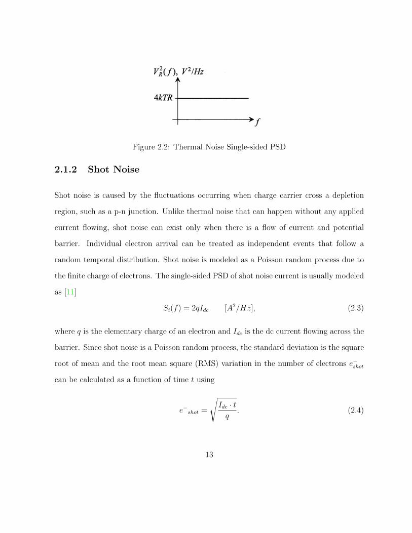
Figure 2.2: Thermal Noise Single-sided PSD
2.1.2 Shot Noise
Shot noise is caused by the fluctuations occurring when charge carrier cross a depletion
region, such as a p-n junction. Unlike thermal noise that can happen without any applied
current flowing, shot noise can exist only when there is a flow of current and potential
barrier. Individual electron arrival can be treated as independent events that follow a
random temporal distribution. Shot noise is modeled as a Poisson random process due to
the finite charge of electrons. The single-sided PSD of shot noise current is usually modeled
as [11]
Si(f) = 2qIdc [A2/Hz], (2.3)
where q is the elementary charge of an electron and Idc is the dc current flowing across the
barrier. Since shot noise is a Poisson random process, the standard deviation is the square
root of mean and the root mean square (RMS) variation in the number of electrons e−shot
can be calculated as a function of time t using
e−shot =
√Idc · tq
. (2.4)
13

2.1.3 Flicker Noise
There are two schools of thought associated with the mechanism that generates flicker noise
in MOS transistors. In McWhorter’s theory, flicker noise is generated when the current
flows near the oxide-semiconductor interface of a MOS transistor. The fluctuation is the
result of many individual trapping and detrapping events that modulate the current [12].
On the other hand, Hooge considered flicker noise a bulk phenomenon generated from
lattice or impurity scattering which causes mobility fluctuations of the charge carriers.
Both theories succeed in partially explaining some of the experimental data. The flicker
noise PSD S1/f (f) is given by [13]
S1/f (f) =kTACoxNt
2τf[(e−)2/Hz], (2.5)
where Nt is the gate oxide trap density per unit volume, A is the area of gate and Cox is
the gate oxide capacitance per unit area. Several models are available in explaining the
wide distribution of traps in both space and energy. The exact meaning of τ depends on
the specific model. Simple models often treat it as the tunneling constant [14]. Thus, the
flicker noise PSD for both the drain current SId(f) and voltage SVg(f) can be generalized
as [15]
SId(f) = g2mSVg(f) = g2m1
C2ox
SQch(f) = g2m1
C2ox
(q
A)2S1/f (f) =
g2mq2kTNt
2C2oxAτf
, (2.6)
where gm is the transconductance of the transistor, SQch(f) is the noise PSD of conducting
channel charges. MOSFET flicker noise can be modeled as a voltage source or current
14

Figure 2.3: Transistor Models of Flicker Noise Source
source as shown in Figure 2.3. SPICE models flicker noise as
Sv(f) =K
CoxWL× 1
f, [
V 2
Hz] (2.7)
where K is a technology-dependent coefficient on the order of 10−25V 2F . From Equa-
tion 2.6, we find that K =q2kTNt
Coxτ. and W and L are the width and length of the
transistor, respectively. Flicker noise has a “pink noise” power density spectrum. Since
the PSD is inversely proportional to frequency, it is usually referred to as 1/f noise.
Over a given bandwidth, we can calculate the RMS flicker noise Vn1/fusing
Vn1/f=
√K
CoxWL× ln(
fhighflow
) (2.8)
where fhigh and flow are the upper and lower frequency limits.
15
2.2 Noise Analysis in Linear Circuits
Noise in a circuit usually comes from multiple sources. We are interested in identifying the
noise contribution of each source and modeling its joint characteristics at a particular node
in the circuit. Assuming noise components are small, we can linearize the circuit model
without considering the change of device operating mode. We now review noise analysis
using two basic examples: integrator and RC circuit before we consider noise of an APS
in Chapter 3.
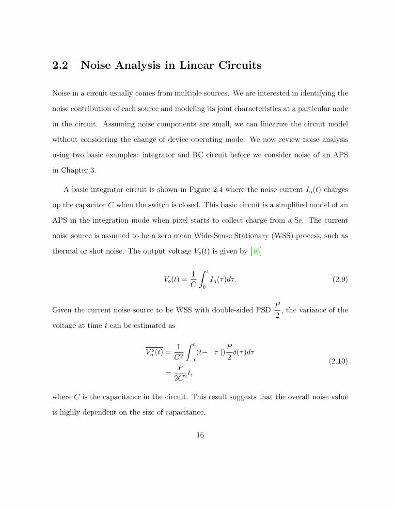
A basic integrator circuit is shown in Figure 2.4 where the noise current In(t) charges
up the capacitor C when the switch is closed. This basic circuit is a simplified model of an
APS in the integration mode when pixel starts to collect charge from a-Se. The current
noise source is assumed to be a zero mean Wide-Sense Stationary (WSS) process, such as
thermal or shot noise. The output voltage Vo(t) is given by [16]
Vo(t) =1
C
∫ t
0
In(τ)dτ. (2.9)
Given the current noise source to be WSS with double-sided PSDP
2, the variance of the
voltage at time t can be estimated as
V 2n (t) =
1
C2
∫ t
−t(t− | τ |)P
2δ(τ)dτ
=P
2C2t,
(2.10)
where C is the capacitance in the circuit. This result suggests that the overall noise value
is highly dependent on the size of capacitance.
16
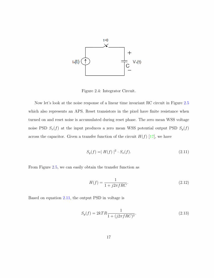
Figure 2.4: Integrator Circuit.
Now let’s look at the noise response of a linear time invariant RC circuit in Figure 2.5
which also represents an APS. Reset transistors in the pixel have finite resistance when
turned on and reset noise is accumulated during reset phase. The zero mean WSS voltage
noise PSD Sx(f) at the input produces a zero mean WSS potential output PSD Sy(f)
across the capacitor. Given a transfer function of the circuit H(f) [17], we have
Sy(f) =| H(f) |2 · Sx(f). (2.11)
From Figure 2.5, we can easily obtain the transfer function as
H(f) =1
1 + j2πfRC. (2.12)
Based on equation 2.11, the output PSD in voltage is
Sy(f) = 2kTR1
1 + (j2πfRC)2. (2.13)
17

Figure 2.5: RC Circuit.
The average output power is calculated as
V 2o =
∫ ∞−∞
2kTR1
1 + (j2πfRC)2df
=2kTR
2πRCarctan(γ) |∞−∞
=kT
C.
(2.14)
It should be noted that the noise is independent of R. This is because resistance is related
to both bandwidth and noise PSD. If the resistance decreases, the bandwidth increase is
inversely proportional to the RC while the noise PSD becomes smaller at the same rate.
In practical circuit environment, we are expecting multiple zero mean, uncorrelated
white noise sources along the signal path as shown in Figure 2.6. Vni represents the input-
referred noise contribution from the following device on the signal path, where i is the
index of noise sources. Assuming that all noise sources are uncorrelated, the average noise
18
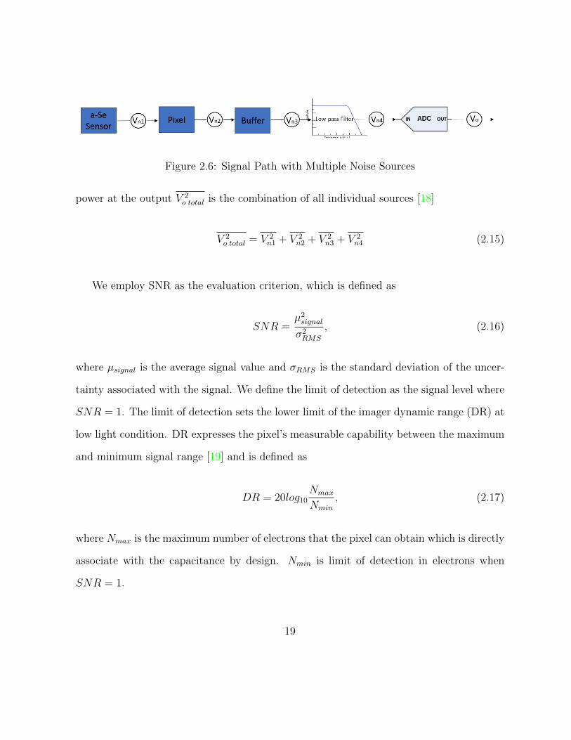
Figure 2.6: Signal Path with Multiple Noise Sources
power at the output V 2o total is the combination of all individual sources [18]
V 2o total = V 2
n1 + V 2n2 + V 2
n3 + V 2n4 (2.15)
We employ SNR as the evaluation criterion, which is defined as
SNR =µ2signal
σ2RMS
, (2.16)
where µsignal is the average signal value and σRMS is the standard deviation of the uncer-
tainty associated with the signal. We define the limit of detection as the signal level where
SNR = 1. The limit of detection sets the lower limit of the imager dynamic range (DR) at
low light condition. DR expresses the pixel’s measurable capability between the maximum
and minimum signal range [19] and is defined as
DR = 20log10Nmax
Nmin
, (2.17)
where Nmax is the maximum number of electrons that the pixel can obtain which is directly
associate with the capacitance by design. Nmin is limit of detection in electrons when
SNR = 1.
19

Chapter 3
Active Pixel Sensor Noise Analysis
In this chapter, we examine the operation of 3T and 4T active pixel sensors. Noise anal-
ysis for each phase of operation is presented. We limit the scope to electrical noise of
APS. Therefore, shot noise generated from photon current by a-Se is not included in the
discussion.
3.1 3T and 4T APS Operation Overview
The most commonly used APS that can achieve non-destructive readout is the 3T struc-
ture shown in Figure 3.1. M1 transistor resets the pixel and a-Se to a reference voltage;
M2 transistor functions as source follower to buffer the signal voltage for non-destructive
readout; and M3 transistor connects individual pixels to a row line. To create a pixel
array, we need to have multiple column lines. Each column line has a bias transistor M5 to
ensure sufficient current going through the line for M2 source follower transistor to operate
21

in the strong inversion mode. Parasitic capacitance and gate capacitance at the input of
gain buffer form a storage capacitor for the signal on column line. After on-chip buffer,
the signal would go off chip and enter PCB as shown in Figure 1.3. A RC filter is placed
between the buffer and ADC in order to filter out any high frequency interference that
couples in the signal. At last, the voltage information from each pixel is digitized into a
16-bit binary number and stored into FPGA memory for further processing.
Figure 3.1: Simplified 3T APS Circuit Model
Three signals are required to output one voltage from the pixel, namely reset Rst, row
select Rs and column select Cs. Multiplexers and decoders increase the control signal
complexity as 6-bit buses are required for a 64-by-64 pixel array. By toggling the state of
each control signal bus, the pixel is able to operate in three phases: reset, integration and
sampling. The timing diagram in Figure 3.2 illustrates the states of each control signal
from FPGA perspective. Only column select is a column-wise operation, while the rest of
22
the signals operate in the unit of rows.
Given Row i has been reset and integrated for a certain period of time, we start from
sampling phase at t1. Rs i is asserted so the on-chip buffer only receives outputs from Row
i from t1 to t3. Cs1 will be asserted at t1 so that pixel(i,1) is connected to the on-chip
buffer for sampling. At t2, Cs1 will be deasserted and Cs2 will be asserted for the same
amount of time so the system is reading pixel(i,2). At t3, the column select bus should go
through all 64 columns on Row i which marks the end of sampling phase for Row i. Rs i
is deasserted and this row will enter reset phase from t4 to t5. Then next row, i+1 will be
selected for sampling from column 1 to 64 from t5 to t6. The integration period for Row i
starts from t5 when it stops being reset till the entire pixel array loops back to sample it
at t1 of the next cycle. The length of this cycle is 63 times the duration from t1 to t5 for
array with 64 rows.
23
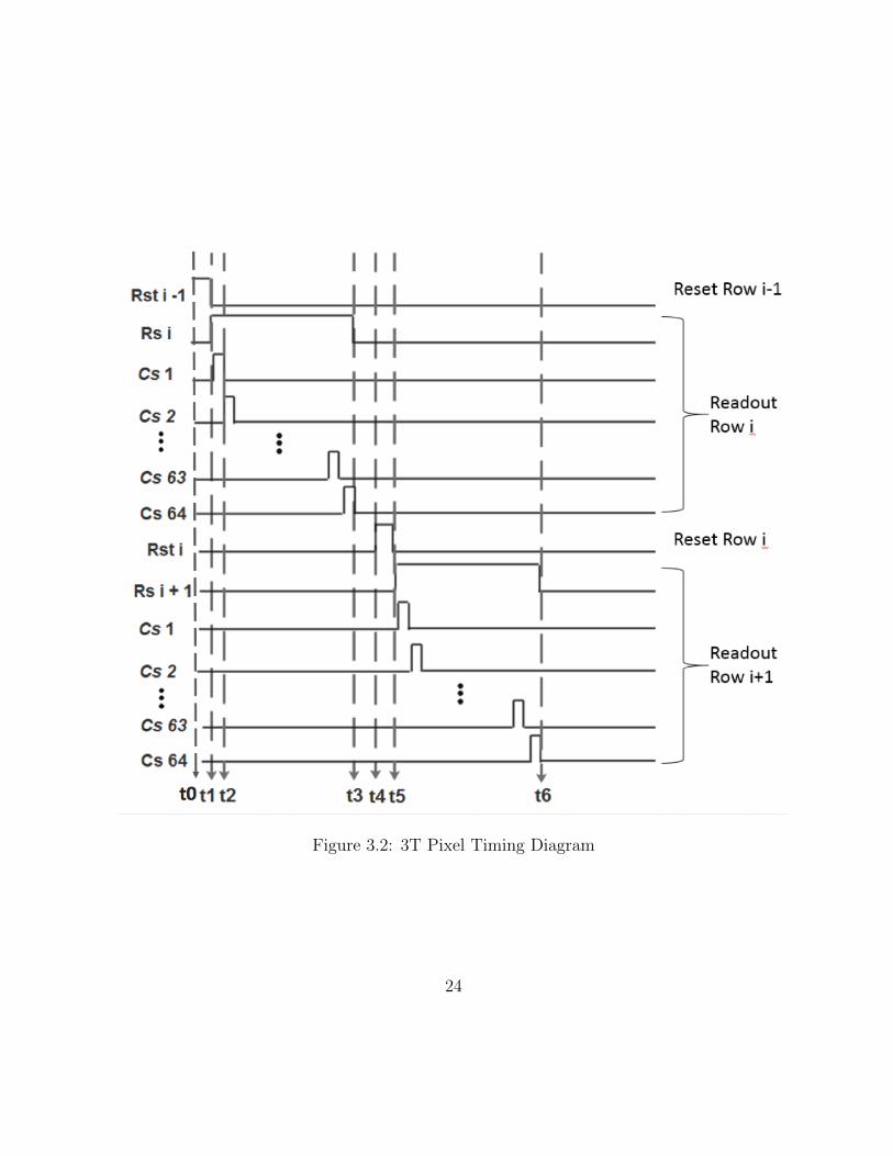
Figure 3.2: 3T Pixel Timing Diagram
24

3.2 3T APS noise analysis
As explained in previous section, the state of the transistor changes with respect to the
phase of operation. To overcome this linear time variant obstacle, noise generated from each
phase of operation is set as the initial condition for the next phase. Assuming that noise
from different phases is uncorrelated, we can apply the summation method in equation 2.15
to produce the final noise value. Analysis of thermal and shot noise in a CMOS APS has
been systematically investigated in [20, 21]. It has been shown that under low exposure
conditions, reset, shot and readout noises dominate. Under high exposure condition, shot
noise introduced by photon generated current becomes the dominant noise component. In
this thesis, we only consider noise from electrical sources, thereby excluding the photon
generated shot noise.
3.2.1 3T APS Phase 1 (Reset)
We start with the reset phase of the pixel. We assume that transistor M1 is completely off
when gate voltage is zero and that rds models the on resistance when Vgate= 3.3V. Between
t0 to t1, M1 transistor turns on to allow the capacitor at the gate of source follower of
the entire row, denoted as Csense, to reset to an external reference voltage. The simplified
model of pixel circuit is shown in Figure 3.3. At the end of tr which is the duration of
reset, M1 is turned off to enclose the pixel for future operation. At this point, we need to
divide the analysis into “soft reset” and “hard reset” based on the operating mode of M1
transistor [22].
Hard reset refers to the reset transistor in the strong inversion mode when the a-Se and
25
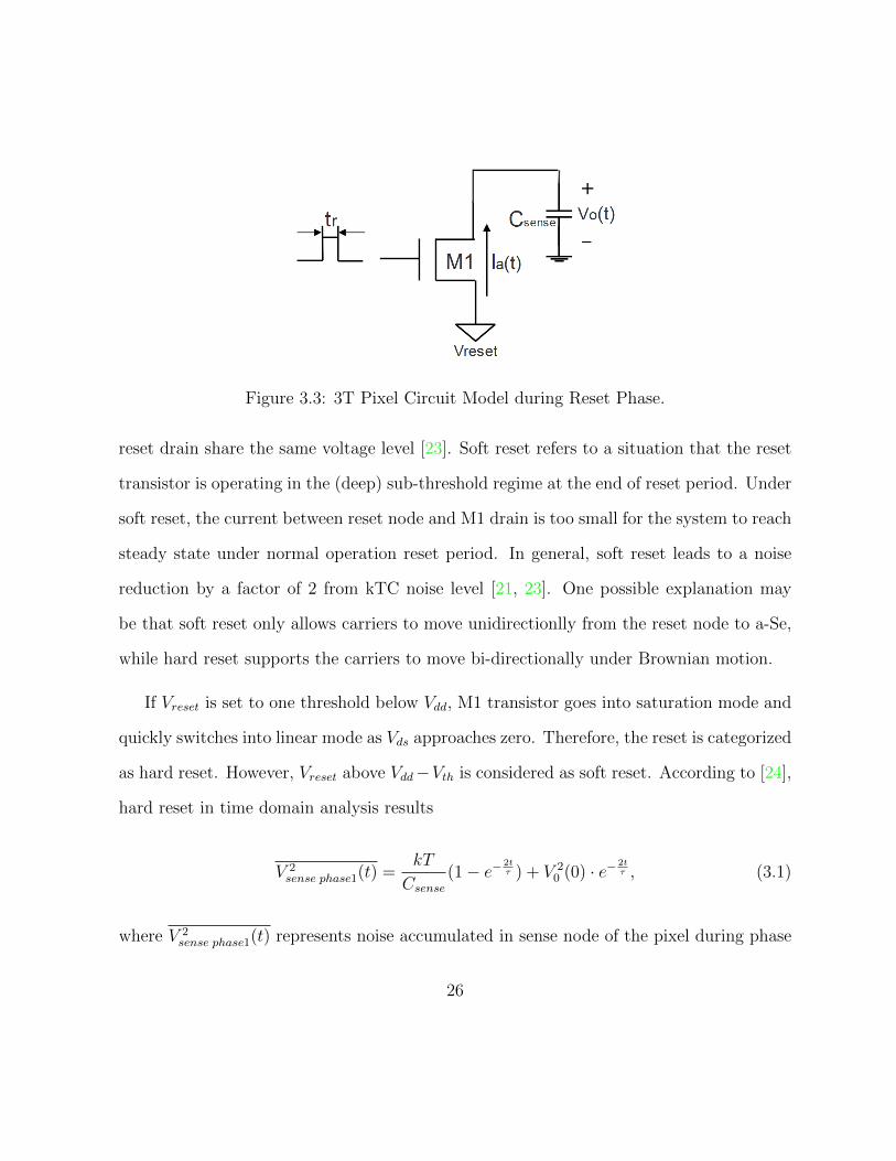
Figure 3.3: 3T Pixel Circuit Model during Reset Phase.
reset drain share the same voltage level [23]. Soft reset refers to a situation that the reset
transistor is operating in the (deep) sub-threshold regime at the end of reset period. Under
soft reset, the current between reset node and M1 drain is too small for the system to reach
steady state under normal operation reset period. In general, soft reset leads to a noise
reduction by a factor of 2 from kTC noise level [21, 23]. One possible explanation may
be that soft reset only allows carriers to move unidirectionlly from the reset node to a-Se,
while hard reset supports the carriers to move bi-directionally under Brownian motion.
If Vreset is set to one threshold below Vdd, M1 transistor goes into saturation mode and
quickly switches into linear mode as Vds approaches zero. Therefore, the reset is categorized
as hard reset. However, Vreset above Vdd−Vth is considered as soft reset. According to [24],
hard reset in time domain analysis results
V 2sense phase1(t) =
kT
Csense
(1− e−2tτ ) + V 2
0 (0) · e−2tτ , (3.1)
where V 2sense phase1(t) represents noise accumulated in sense node of the pixel during phase
26
1.
Assuming that reset period is much longer than the time constant, Equation 3.1 can be
reduced to V 2sense phase1(t) =
kT
Csense
which can be derived from frequency domain analysis.
On the other hand, soft reset in time domain is [25]
V 2sense phase1(t) =
kT
2Csense
(1− (kTCsense
qIa(0)t)2) + V 2
0 (0) · (kTCsense
qIa(0)t)2, (3.2)
where Ia(0) is the drain current of M1. Under the similar assumption on the duration of
reset period, soft reset yieldskT
2Csense
.
In our imager, if M1 operates in sub-threshold mode, the reset can be considered as
soft reset while any voltage below this value would be considered as hard reset. A more
detailed numerical analysis will be provided in chapter 4.3 with the consideration of body
effect.
3.2.2 3T APS Phase 2 (Integration)
Integration period occurs between reset (t5) and sampling phases (t1 in the next cycle
in Figure 3.2). Usually it lasts for tens of ms, which is much longer than other phases.
During this phase, any signal generated from the a-Se would be accumulated into Csense.
In this thesis, we keep our focus on electrical noise characteristic, therefore neglecting the
change in this phase. However, as we will discuss in later chapter, there is leakage current
from both the protection diode and M1 reset transistor. Instead of shot noise generated
from photo current, we will include shot noise associated with leakage current and how
it is distributed to the capacitor in the pixel. Leakage current is particularly difficult
27
to calculate because we know from experiment that it is in the order of femto Ampere
and the models provided by the manufacture could be off by a few orders due to other
physical parameters. However, by randomly selecting a few pixels and observing closely
the rate of change in pixel value, we can estimate the leakage current in all quadrants.
From Equation 2.4, the noise electron value is proportional to the integration time and the
amount of current. As a result, at the end of integration phase, the overall noise power is
the sum of first phase and shot noise generated in this phase as shown in Equation 3.3
V 2sense phase2 = V 2
sense phase1 + V 2sense shot, (3.3)
where Vsense phase2 represents noise accumulated at sense node during phase 2 and Vsense shot
represents shot noise at sense node.
3.2.3 3T APS Phase 3 (Sampling)
Sampling phase starts from t5 till all the columns have been asserted and deasserted. The
first sample is taken a few clock cycles after Rs i + 1 and Cs 1 are selected. This delay is
calculated to ensure the voltage in pixel(i, 1) is stable before passing onto the on-chip buffer.
Voltage signal at the gate of M2 source follower is translated to the source and stored in
the column line capacitor Ccol. M5 current bias transistor is always on to provide stable
current and make sure that the column line is responsive for the duration of sampling.
On-chip buffer continuously reads the voltage signal on Ccol and drives it off the chip onto
PCB. In our case, there is only charge generated from dark current and leakage current.
On noise aspect, we first need to identify the noise contribution along the signal path. The
28
column line referred thermal noise value introduced by M2, M3 and M5 can be calculated
as [16]
V 2thermal,M2 =
2
3
kT
Ccol
1
1 + gm2
gd3
(3.4)
V 2thermal,M3 =
kT
Ccol
1
gd3
(1gd3
+ 1gm2
) (3.5)
V 2thermal,M4 =
2
3
kT
Ccol
gm4
(1
gd3+
1
gm2
), (3.6)
where gm is the small signal gain and gd3 is channel conductance of the device. Since both
M3 and M4 serve as NMOS switch to connect the circuit, they share the same thermal
noise PSD. For simplicity, we sum up these noise sources on the column line based on
superposition formula in Equation 2.15.
Next, we look at flicker noise generated from M3, M4 and M5. According to the
operation time in the previous section, M3 is on only when both M4 and M5 are selected.
Therefore, we can set the upper limit of frequency as the clock rate of the chip while the
lower limit is given by the row select signal for M2, M3 and M4. However, we know that
M5 is always on to provide bias current for the entire array. Due to the extended operating
time, it is particularly susceptible to the flicker noise. We calculate noise by comparing the
deviation between each sample and the sample mean. Therefore, the lower frequency limit
of M5 is the integration time of the pixel, which is significantly larger than row select time.
Using Equation 2.8, we can calculate the flicker noise for all the transistors on column line
and add them onto Vpath.
Last, voltage signal is driven off the chip for PCB level processing. In our design, we
29

have another unity gain buffer to maintain drive strength, followed by a simple RC filter
to limit the bandwidth of the signal. Then the signal is quantized by a 16-bit successive
approximation ADC, which outputs the digital signal to FPGA memory. Theoretically,
the signal path noise should be one order of magnitude lower than the noise from the pixel
in order for effective quantization. However, our PCB design has some significant noise
contributions, denoted as Vboard, to the final noise reading. These contributions will be
discussed in later chapters.
3.2.4 3T APS Summary
We have walked through the operation of imaging cycle and analyzed the noise contribution
from each phase. We assume that the supporting circuit on PCB produces negligible noise
compared to the noise generated by the APS circuit. During reset phase, M1 reset transistor
generates thermal noise based on two types of reset modes. Next, the leakage current from
both the protection diode and the M1 transistor brings in shot noise during integration
period. Sampling phase includes noise generated from the devices along the signal path as
well as noise from PCB level components. As mentioned in section 3.2, we use the noise
value of the current phase as the initial condition for the next phase and all noise sources
are summed up as given by equation 2.15. Therefore, the final noise value from the 3T
APS is
V 2final = V 2
reset + V 2integrate + V 2
sampling + V 2signalpath + V 2
PCB. (3.7)
The overall noise strength is the summation of noise from reset phase, integration phase,
sampling phase, on-chip signal path and the PCB components.
30

Figure 3.4: Simplified 4T APS Circuit Model
3.2.5 4T APS Structure and Operation
In the 4T pixels on the CMOS chip, an extra transistor M2 exists between a-Se and the
gate of the source follower as Figure 3.4. This transistor enables correlated double sampling
(CDS), where the pixel can output both reset level and the summation of reset and signal
generated by a-Se.
Since 4T pixel is more complex, it is beneficial to delve into the timing digram and
operation from pixel perspective as shown in Figure 3.5. Row i first goes through reset
by turning M1 reset and M2 transfer transistor on from t0 to t1. Soon after the M1
turns off, the transfer gate also turns off at t2 to separate the reset node and a-Se. Reset
node employs parasitic capacitance as Csense while Cint is a metal-insulator-metal (MIM)
capacitor. From t2, integration of Row i starts and continues till Rs i is selected. From
31

Figure 3.5: 4T Pixel Timing Diagram
t3, Cs j is asserted to produce the first sample, which is the reset level from pixel(i, j).
Half way through sampling phase of Row i, Tx i turns on M2 to connect capacitor Cint
and Csense back together. Charge generated from a-Se during integration is transferred to
Csense. Cs j is asserted again to produce the second sample in pixel(i, j), which is the
combination of reset and accumulated charge signal.
From Figure 3.2, we can easily see that each column on the same row is sampled at
different time which means pixel (i, 64) will always have longer integration time comparing
to pixel (i, 1) as the entire row reset. However, because integration duration is much longer
than the time difference between columns, the overall signal level only have 0.2% offset in
the worst case scenario.
32

3.3 4T APS noise analysis
3.3.1 4T APS Phase 1 (Reset)
As each transistor in pixel turns on or off, the capacitance to certain node changes, which
sequentially changes the noise value as well. 4T APS operation is as shown in Figure 3.5,
M2 transfer gate also takes its part from t0 to t2 in reset phase. M1 and M2 turn on
together at t0 to reset the voltage in both Csense and Cint to the reference level. At t1, M1
reset transistor turns off, generatingkT
Csense + Cint
orkT
2(Csense + Cint)reset noise in pixel.
Figure 3.6: Circuit Model during Transfer Gate Turns Off.
At the end of t2, M2 turns off and the circuit can be modeled as in Figure 3.6. Given
that the reset noise voltage iskT
Csense + Cint
, the noise charge in Coulombs can be computed
as
Q2n total = (Csense + Cint)
2V 2n reset
= (Csense + Cint)2 kT
Csense + Cint
= kTCsense + kTCint.
(3.8)
33

The electrons previously stored in the pixel due to noise are distributed proportionally by
the size of capacitors on each side of M2 as it turns off at t2
Q2sense
C2sense
=Q2
int
C2int
. (3.9)
At this point, there is no new source of noise added into the pixel and noise charge can be
summed in quadrature as
Q2sense +Q2
int = Q2total. (3.10)
Combining Equation 3.9 and Equation 3.10, we have
Q2
sense =Q2
totalCint
Csense+ 1
Q2int =
Q2total
CsenseCint
+ 1
(3.11)
where Q2sense, Q
2int and Q2
total are the noise charge stored in the sense node, in the integration
node and in the pixel respectively.
By solving the system of equations, we can estimate the noise in electron stored in each
capacitor. However, we can only verify the noise value at Csense because the capacitor Cint
is not attached to any readout path. It is technically impossible to single out the voltage
value without recombining the charge in Csense. In addition, the size of capacitors are in
femto Farad, making the overall noise value very sensitive to the exclusion of any noise
source.
34

Figure 3.7: Leakage Current in 4T APS Circuit
3.3.2 4T APS Phase 2 (Integration)
We have shown that the only noise source that matters during integration phase is shot
noise from the protection diode and the M1 transistor. Since the M2 transfer gate is
placed between Csense and Cint, the leakage current from the protection diode as shown
in Figure 3.7 can no longer flow into the sense node easily which changes the noise value
for the two samples produced by 4T APS. The first sample with M2 turned off has little
leakage current from both M1 and M2 while the second reading with M2 turned on receives
the same amount of shot noise as 3T APS. Unfortunately, leakage current is difficult to
accurately estimate by simulation tools. Nevertheless, we start with the result from SPICE
simulation, a value of 1fA, as a rough estimation on the leakage current. Here we denote the
35
shot noise from leakage current accumulated in Cint as Vleak int and shot noise accumulated
at the gate of source follower as Vleak sense
I2leak total = I2Leak int + I2leak sense (3.12)
V 2leak total =
ILeak total · tCsense + Cint
(3.13)
where I2leak sense, I2Leak int and I2Leak total are the noise charge generated from leakage current,
that are stored in the sense node, in the integration node and in the pixel respectively.
V 2leak total is the shot noise accumulated within the pixel in voltage .
3.3.3 4T APS Phase 3 (Sampling)
Noise from signal path is the same as 3T APS, which we have already covered in Sec-
tion 3.2.3. It is worth mentioning that we can achieve CDS from two non-destructive
readings: reset and read by turning on M2 at t4. The basic intention of CDS has been
the elimination of kTC reset noise and the reduction of 1/f noise generated in the output
buffer by subtracting 2 correlated pixel samples. The difference between normal imaging
operation and CDS is that the time between samples reduces from one integration period
down to the sampling gap which is from t3 to t4 shown in Figure 3.5. This relatively small
time gap is to ensure the correlation of samples. In brief, CDS can be described as an
autozeroing operation followed by a sample and hold operation. CDS, however, doubles
the noise power of the broadband (i.e.,white) noise, since one pixel is sampled twice and
subtracted in each imaging cycle [26].
36

3.3.4 4T APS Summary
We have elaborated 4T APS imaging cycle and analyzed the noise contribution in each
phase of the operation. We assume that the support circuits on PCB produces negligible
noise compared to the noise generated by APS circuit. In reset phase, M1 reset transistor
generates thermal noise and M2 transfer gate separates the noise electrons into Csense and
Cint. During integration phase, there is certain amount of leakage current from both the
protection diode and the M1 transistor. Sampling phase includes thermal noise and flicker
nosie generated from the devices along the signal path as well as noise from PCB level
components. As mentioned in section 3.2, we would use the noise result of current phase
as the initial condition for the next phase and all noise source would be summed up by
superposition. Therefore, the final noise value of two readings are given as
V 2reset = A2((
Qsense
Csense
)2 + V 2leak sense) + V 2
signalpath + V 2PCB
V 2read = A2
[(
Qn total
Csense + Cint
)2 + V 2leak sense
]+ V 2
signalpath + V 2PCB
V 2CDS = A2
[(
Qn total
Csense + Cint
)2 − (Qsense
Csense
)2 + V 2leak total
]+ 2(V 2
signalpath + V 2PCB)
(3.14)
where A is the gain of the on-chip signal path.
37

3.4 Summary
There are four quadrants in the chip with some transistor level variations. Q1 employs
all NMOS devices and Csense is parasitic capacitance. M2 and M4 in Q2 are transmission
gates to compensate charge injection effect when turning off devices. Q3 is the only 3T
APS in the chip while Q1 and Q4 are much alike. Detailed design of each quadrant is
explained in Chapter 4. Noise analysis for both 3T and 4T pixel are presented for different
phases.
38

Chapter 4
Simulation and Measured Result
Comparison
In this chapter, we first conduct an experiment to measure the noise performance of the
CMOS imager. The experimental results are then compared with the system simulation
in Cadence.
4.1 Details of the Device under Test
We perform experiments on each quadrant of the CMOS imager. The architecture of
Quadrant 1 (Q1) is illustrated in Figure 3.4. Q1 employs only NMOS transistors. Source
follower is a native device with zero threshold voltage to allow maximum voltage swing.
To prevent damaging the pixel from excessive signal accumulation during exposure, a P-N
junction diode is connected between Cint and Vdd in reverse bias to provide an upper limit
39

for voltage level. Once the voltage level in Cint exceeds Vdd + 0.7V, extra electrons will
flow through the diode to Vdd.
(a) Quadrant 1 Pixel Schematic (b) Quadrant 2 Pixel Schematic
Figure 4.1: Pixel Schematic Screen Captures in Cadence
Quadrant 2 (Q2) replaces M2 and M4 with transmission gate to allow bigger voltage
swing. Rather than using parasitic capacitance for Csense, a metal-insulator-metal (MIM)
capacitor is placed at the gate of M3 to achieve higher controlled capacitance. Minimum
allowable size of MIM cap is 4µm × 4µm. Therefore, the capacitance is approximately
16 fF on the drain and source of M2. With one more capacitor in the pixel, Quadrant
2’s size becomes twice as wide as other quadrants with only one MIM cap. With PMOS
transistor in transmission gate, there is an implicit P-N junction diode connected both the
drain and the source of PMOS. Therefore, there is no need for an explicit protection diode
to be placed between Cint and Vdd. Leakage current in Q1 floats through M2 transfer gate
and charges up Csense. And leakage current in Q2 charges up both Cint and Csense at the
same rate.
40
(a) Quadrant 3 Pixel Schematic (b) Quadrant 4 Pixel Schematic
Figure 4.2: Pixel Schematic Screen Captures in Cadence
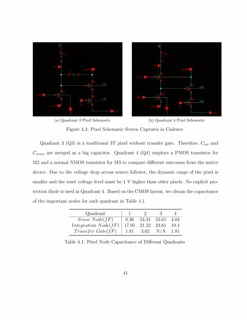
Quadrant 3 (Q3) is a traditional 3T pixel without transfer gate. Therefore, Cint and
Csense are merged as a big capacitor. Quadrant 4 (Q4) employs a PMOS transistor for
M2 and a normal NMOS transistor for M3 to compare different outcomes from the native
device. Due to the voltage drop across source follower, the dynamic range of the pixel is
smaller and the reset voltage level must be 1 V higher than other pixels. No explicit pro-
tection diode is used in Quadrant 4. Based on the CMOS layout, we obtain the capacitance
of the important nodes for each quadrant in Table 4.1.
Quadrant 1 2 3 4Sense Node(fF ) 6.36 24.31 23.61 4.04
Integration Node(fF ) 17.95 21.22 23.61 19.4Transfer Gate(fF ) 1.81 3.62 N/A 1.81
Table 4.1: Pixel Node Capacitance of Different Quadrants
41
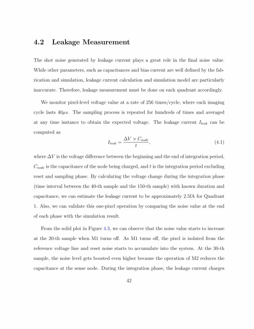
4.2 Leakage Measurement
The shot noise generated by leakage current plays a great role in the final noise value.
While other parameters, such as capacitances and bias current are well defined by the fab-
rication and simulation, leakage current calculation and simulation model are particularly
inaccurate. Therefore, leakage measurement must be done on each quadrant accordingly.
We monitor pixel-level voltage value at a rate of 256 times/cycle, where each imaging
cycle lasts 40µs. The sampling process is repeated for hundreds of times and averaged
at any time instance to obtain the expected voltage. The leakage current Ileak can be
computed as
Ileak =∆V × Cnode
t, (4.1)
where ∆V is the voltage difference between the beginning and the end of integration period,
Cnode is the capacitance of the node being charged, and t is the integration period excluding
reset and sampling phase. By calculating the voltage change during the integration phase
(time interval between the 40-th sample and the 150-th sample) with known duration and
capacitance, we can estimate the leakage current to be approximately 2.5fA for Quadrant
1. Also, we can validate this one-pixel operation by comparing the noise value at the end
of each phase with the simulation result.
From the solid plot in Figure 4.3, we can observe that the noise value starts to increase
at the 20-th sample when M1 turns off. As M1 turns off, the pixel is isolated from the
reference voltage line and reset noise starts to accumulate into the system. At the 30-th
sample, the noise level gets boosted even higher because the operation of M2 reduces the
capacitance at the sense node. During the integration phase, the leakage current charges
42
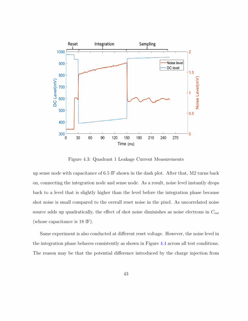
Figure 4.3: Quadrant 1 Leakage Current Measurements
up sense node with capacitance of 6.5 fF shown in the dash plot. After that, M2 turns back
on, connecting the integration node and sense node. As a result, noise level instantly drops
back to a level that is slightly higher than the level before the integration phase because
shot noise is small compared to the overall reset noise in the pixel. As uncorrelated noise
source adds up quadratically, the effect of shot noise diminishes as noise electrons in Cint
(whose capacitance is 18 fF).
Same experiment is also conducted at different reset voltage. However, the noise level in
the integration phase behaves consistently as shown in Figure 4.4 across all test conditions.
The reason may be that the potential difference introduced by the charge injection from
43

Figure 4.4: Quadrant 1 Noise Behavior vs Various Reset Voltages
M1 or M2 turning off is resilient to the change of reset voltage. This hypothesis is evident
by the experimental results in Figure 4.5. Therefore, leakage current flowing into the sense
node by constant potential different should be close to the value calculated in [27]. On the
other hand, we know that the protection diode is placed in reverse bias. Leakage current
through the diode is exponentially proportional to the potential difference across the P-N
junction. Therefore, by measuring the voltage change after the integration period, we see
a decreasing trend in leakage current as the reset voltage increases.
It is noteworthy that in the case of Vreset = 1.9V and 2.0V, the noise value at the end
of integration is lower than results from other reset voltages because the transistor has
44

1 1.1 1.2 1.3 1.4 1.5 1.6 1.7 1.8 1.9 2Reset Voltage (V)
100
200
300
400
500
600
700
800
Vds
(mV
)
20
30
40
50
60
70
80
90
100
M2 onM2 offM1 off
Figure 4.5: Quadrant 1 Voltage Drop due to Charge Injection vs Various Reset Voltages
difficulty in conducting such high voltage. We also observe the big ramps on noise value
at sampling phase while others are relatively flat. This behavior is unexpected since there
is no transistor toggling. The swing in noise value also exhibits across other quadrants,
which dramatically affects our experimental noise measurement.
Looking further into this phenomenon, we extend our tests with fixed reset voltage and
vary the test duration, mainly the period when the swing starts. Figure 4.6 shows the test
results after the swing begins, from which we can observe that various integration durations
overlap quite well, forming a shape that resembles a sinusoidal signal. This indicates that
there are some low-frequency signals interfering with the signal path. Possible sources
could be the fluctuation introduced by grounding and power supply. We will discuss on
this issue in detail and provide solutions to suppress the variation in the next chapter.
One of the objectives of the experiment is to find out the amount of leakage current in-
45
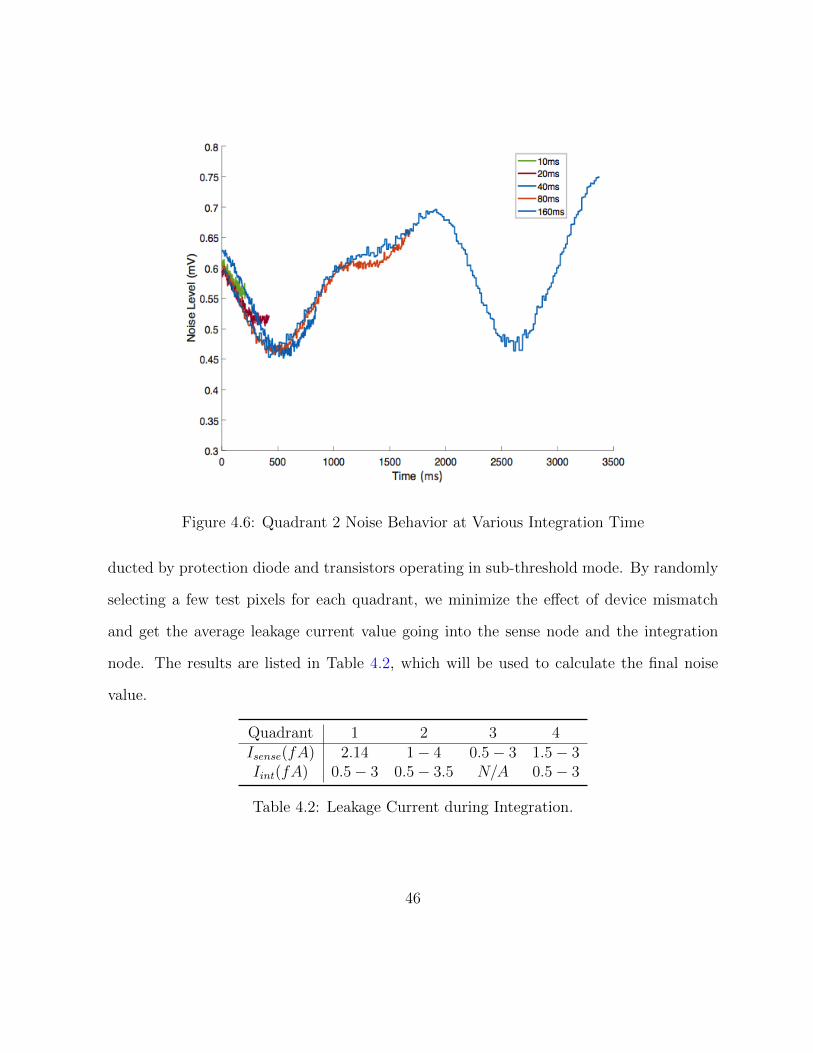
Figure 4.6: Quadrant 2 Noise Behavior at Various Integration Time
ducted by protection diode and transistors operating in sub-threshold mode. By randomly
selecting a few test pixels for each quadrant, we minimize the effect of device mismatch
and get the average leakage current value going into the sense node and the integration
node. The results are listed in Table 4.2, which will be used to calculate the final noise
value.
Quadrant 1 2 3 4Isense(fA) 2.14 1− 4 0.5− 3 1.5− 3Iint(fA) 0.5− 3 0.5− 3.5 N/A 0.5− 3
Table 4.2: Leakage Current during Integration.
46
4.3 Signal Path Measurement
Signal path for imagers is defined as the shared components between the row-line transistor
and the digital side of ADC. Signals coming out of the pixels share the column line, on-
chip amplifier and the rest of PCB devices. The reason for sharing is to reduce the design
complexity while fitting a set of strict timing constrains. Another advantage of sharing is
the simplified bring up and analysis in the experimental phase of the project. However,
the shared path sets a minimum integration period for loading outputs from devices. In
general, the signal path of a imager is usually designed to have noise contribution one order
less than the imager for noise characterization. This chip has an unity gain buffer, an RC
filter and a 16-bit ADC on the PCB. Each of them is selected to have less than 50µV
noise contribution. Assuming noises generated from the components along the signal path
are independent, the overall noise value introduced by the signal path remains very small
comparing to the noise generated from the pixel.
On the PCB level, it is easy to use the testpoint connector to apply a DC voltage for
testing noise performance of each component. On IC level, we can also lock down to one
pixel and keep M4 and M5 transistor on. By applying the reset voltage as reference, we
can obtain the stationary noise contribution of the pixel as well. However, this is not the
best way to mimic normal operation because none of the row select and column select
transistor is toggling.
In this experiment, the chip is configured to rapidly take 4 samples per pixel during
each sampling period. To account for signal settling, only the middle two samples are
used to subtract each other. Since the data is taken within a very shot period of time,
47
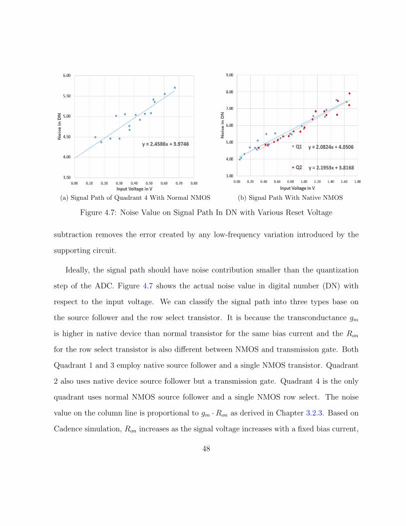
(a) Signal Path of Quadrant 4 With Normal NMOS (b) Signal Path With Native NMOS
Figure 4.7: Noise Value on Signal Path In DN with Various Reset Voltage
subtraction removes the error created by any low-frequency variation introduced by the
supporting circuit.
Ideally, the signal path should have noise contribution smaller than the quantization
step of the ADC. Figure 4.7 shows the actual noise value in digital number (DN) with
respect to the input voltage. We can classify the signal path into three types base on
the source follower and the row select transistor. It is because the transconductance gm
is higher in native device than normal transistor for the same bias current and the Ron
for the row select transistor is also different between NMOS and transmission gate. Both
Quadrant 1 and 3 employ native source follower and a single NMOS transistor. Quadrant
2 also uses native device source follower but a transmission gate. Quadrant 4 is the only
quadrant uses normal NMOS source follower and a single NMOS row select. The noise
value on the column line is proportional to gm ·Ron as derived in Chapter 3.2.3. Based on
Cadence simulation, Ron increases as the signal voltage increases with a fixed bias current,
48
which explains the trends for all three plots. Although Ron does not increase linearly with
signal voltage, the small operating range of signal voltage does allow us to linearize the
final noise value. Furthermore, the results in Figure 4.7 include noise generated from two
sampling operations. Therefore, normal sampling should be√
2 orders less than the values
in Figure 4.7.
From Chapter 3.2.3, noise value generated by devices on column line at 1V is about
2 DN, which is significantly smaller than noise generated from Phase reset and Phase
integration combined. Yet the measurement from this experiment is much bigger than
the design objective. This indicates that there must be additional noise along the signal
path. We will investigate the causes further more in the next chapter. For now, we use the
functions that fit the experimental results to calculate how much the signal path contribute
to the final noise value at different reset voltage levels.
4.4 Normal Operation Measurement
4.4.1 Operation Parameters Setup
In the normal operation mode, there are two free parameters: reset voltage and integration
time. Low reset voltage provides a wide dynamic range for a large amount of photonic
signal. Integration time is the period between t2 and t3 in Figure 3.5. From noise mea-
surement perspective, increasing reset voltage causes reset transistor to operate from triode
to sub-threshold region. We expect to observe a drop in noise value and verify whether
it yieldskT
2Creset noise as presented in [21]. Increasing integration time increases shot
49
noise as a result of larger leakage current accumulation, which in turn increases the final
noise value. The shortest stable integration time for this system is defined to be 30 µs,
which fulfills 30 frame per second as one of the prime design requirements. In our scope
of measurement, we start taking samples from 40 µs to 160 µs integration time, with a
step size of 20 µs. Also, each set of integration time covers different reset voltage levels,
ranging from 0.6 V to 2.2 V depending on the maximum and minimum voltage that pixel
structure can obtain. For example, Q1 employs parasitic capacitor sized about 5.6fF at the
sense node. When M1 NMOS reset transistor and M2 NMOS transfer transistor are being
turned off, part of mobile electrons are injected into the sense node, resulting a decrease in
voltage. If the reset voltage is set to be lower than 0.8V, the resulting voltage drops as low
as 0.1V, which on chip amplifier will not be able to output. On the other hand, M2 and
M4 in Q2 are transmission gates. They not only minimize the effect of charge injection
but also allow higher voltage to be outputted with respect to single NMOS structure.
The body effect plays a significant role at high reset voltage levels for both reset and
row select transistor. For simplicity, it is commonly assumed that the threshold voltage
is about 0.7V if the source and the bulk of the transistor are tied together. However,
it is not the same case in our design. Body effect refers to the change in the transistor
threshold voltage resulting from a non-zero voltage difference between the transistor source
and body. Because the voltage difference between the source and body affects the threshold
voltage, the body canbe considered as a second gate that determines the operation mode
of the transistor. The threshold voltage VTH can be calculated as
VTH = VT0 + γ(√|Vsb + 2φF | −
√|2φF |), (4.2)
50

where VT0 is the threshold voltage of the long channel device at zero substrate bias, γ
is a process parameter called the body-effect coefficient, and φF is a physical parameter
(2φF ≈ 0.6V for NMOS). From Cadence simulation, we can calculate the threshold voltage
for both reset and row select transistor. With high reset level, we can determine at which
voltage level the reset transistor operates at sub-threshold mode. The maximum voltage
that row select transistor can pass as a switch is one threshold below supply voltage. Any
input voltages above this value is not suitable for noise consideration. Therefore, the
maximum voltage for the reset transistor to remain in saturation region is about 1.9 V and
the associate threshold voltage is 1.3 V.
4.4.2 Quadrant 1 Measurement
Knowing the uncertainty of leakage current and some PCB issues on this prototype as
described in Chapter 3 and Chapter 4, we now can examine the measured result and
compare it with the simulation. Each pixel at sampling phase produces two outputs after
integration, denoted as reset and read accordingly. For quick recapitulation of noise, sample
reset contains a portion of reset noise, some amount of shot noise from leakage current,
and noise generated from the readout path. Sample read contains all of reset noise, shot
noise from leakage and readout path noise as well, yet the noise value in voltage is smaller
than sample reset. It is because reset is sampled from a parasitic capacitor while read is
sampled from a node combined with parasitic and a much larger MIM capacitor.
Figure 4.8 shows the noise value of sample reset in Q1, where the x-, y-, and z-axis
represent the reset voltage, integration duration, and noise value. Noise value from both
51

16
18
20
22
24
26
28
Noi
se V
alue
(DN
)
30
32
34
1501.9
1.8100
Integration Time(ms)
1.7
Vreset(V)
1.650 1.51.4
0 1.3
MeasuredSimulation
Figure 4.8: Quadrant 1 Sample Reset Measurement vs Simulation
52
results increase with respect to integration duration because shot noise from leakage ac-
cumulates over time. Furthermore, the size of parasitic capacitance is very small which
stores only about 34 e− after M2 turns off while shot noise at this node increases from 35
e− to 70 e− for different integration time. Therefore, the contribution of shot noise toward
the overall noise value increases considerably. From reset voltage perspective, we expect
to see a small drop at 1.85V because the reset noise from sub-threshold reset is halved
as illustrated by the green surface in Figure 4.8. However, it is not the case in measured
results. It is because reset noise is no longer the greatest noise contribution. Also, we have
to address the large gap between the measured and simulation results because the size of
parasitic capacitance is hard to estimate. Any small change of noise component in this
small capacitance would result in a large deviation on the final noise value.
We now turn our focus on the read sample noise value. As it is illustrated in Figure 4.9,
the increase of noise value over integration reduces from 8DN in the reset plot to less than
2 DN in the simulation. The change arises from much bigger capacitor connecting to the
node as transfer gate turns back on. The discrepancy between simulation and measurement
also reduces from 6 DN to 3 DN because MIM capacitor has a more well-controlled size.
In this plot, we observe a noise value reduction at high reset level. However, this quadrant
employs a single NMOS as row select. Output as high as 1.85 V is close to the upper limit
of its signal path. Therefore, it is not sufficient to conclude that the result is a consequence
of the half reset noise theory.
53

8
9
10
200
11
12
13
14
Noi
se V
alue
(DN
)
15
16
17
150
Integration Time(ms)
1002
1.81.6
Vreset(V)
50 1.41.2
10 0.8
MeasuredSimulation
Figure 4.9: Quadrant 1 Sample Read Measurement vs Simulation
54

4.4.3 Quadrant 2 and 3 Measurement
8
10
200
12
14
16
No
ise
Va
lue
(DN
)
18
150
20
Integration Time(ms)
1002.221.8
Vreset(V)
50 1.61.41.210.80 0.6
Simulation
Measured
(a) Quadrant 2 Sample Reset
7
8
9
160
10
11
12
13
14
No
ise
Va
lue
(DN
)
140
15
16
17
120
Integration Time(ms)
100
80 2.221.8
Vreset(V)
60 1.61.41.2140 0.80.6
Simulation
Measured
(b) Quadrant 2 Sample Read
Figure 4.10: Quadrant 2 Measurement vs Simulation
Fortunately, Q2 employs a transmission gate as row select that can pass rail to rail
voltage to on-chip buffer. Q2 also contains a MIM capacitor on both the sense node and
the integration node. It should be able to achieve the lowest noise in voltage among all
quadrants. However, due to a series of known design defects, the noise value can only be
reduced to 13 DN. The discrepancy between simulation and measurement comes from many
sources. First, some noise sources are particularly difficult to accurately measure because
of the stuck code issue of ADC described in Chapter 5.1. This results an underestimation
of noise value in simulation. For low noise pixels such as Q2, the impact of PCB level
interference stands out as both reset noise and shot noise component reduce. On the other
hand, we observe a large noise reduction in measurement as the reset level goes beyond
55
1.85 V. Thanks to the transmission gate, we can confirm the readout over 1.85 V is still
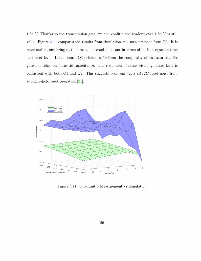
valid. Figure 4.11 compares the results from simulation and measurement from Q3. It is
more stable comparing to the first and second quadrant in terms of both integration time
and reset level. It it because Q3 neither suffer from the complexity of an extra transfer
gate nor relies on parasitic capacitance. The reduction of noise with high reset level is
consistent with both Q1 and Q2. This suggests pixel only gets kT/2C reset noise from
sub-threshold reset operation [21].
8
10
12
160
14
16
18
Noi
se V
alue
(DN
)
20
1402120 1.8100
Integration Time(ms)
1.61.4
Vreset(V)
80 1.2160 0.8400.6
Simulation
Measured
Figure 4.11: Quadrant 3 Measurement vs Simulation
56

4.4.4 Quadrant 4 Measurement
Q4 employs PMOS as M2 transfer gate and normal device as source follower. It should
be noted that the reset voltage starts at 1.65 V due to 0.85 V Vgs drop in Figure 4.12a,
suggesting that the dynamic range of this quadrant is smaller than the others. For sample
reset plot on the left, it is the first time that the simulation value is higher than the
measurement from 1.6 V to 1.7 V, even though the increasing trend along integration
time is still compliant. We address this discrepancy to the charge injection of the M1 and
M2 transistor. While other quadrants use NMOS for both reset and transfer gate, Q4 has
NMOS and PMOS for M1 and M2 transistor. NMOS transistor ejects electrons during shut
off while PMOS ejects holes. It is the same principle to use identical sized transmission
gate to neutralize the impact of charge injection. As voltage increases, we do not observe
any drop in final value due to the reduction of reset noise, causing by the same reason
from Q1 sample reset. The parasitic capacitance at sense node is small enough such that
the shot noise from leakage dominates the node. Measurement of sample read is consistent
with simulation and noise value is lower than other quadrant despite it suffers the same
design fault on signal path. It is worth mentioning that normal source follower also reduces
the gain of pixel from 0.9 to 0.7, suggesting the input-referred noise value looks a bit larger
than what is on the figure. With 0.85 V of threshold voltage, charge injection and gain of
0.7, the output of pixel is between 0.27 V to 0.7 V with reset level ranging from 1.6 V to
2.2 V. Such pixel voltage level is within the range of output for the row select and the on
chip buffer, which means the noise measurement from output is valid as well.
57

15
16
17
18
160
19
20
21
22
No
ise
Va
lue
(DN
)
23
24
25
140 2.32.2120 2.1
Integration Time(ms)
100 2
Vreset(V)
80 1.91.860 1.740 1.6
SimulationMeasured
(a) Quadrant 4 Sample Reset
6.5
7
7.5
8
8.5
9
200
9.5
No
ise
Va
lue
(DN
)
150100
Integration Time(ms)
2.32.22.1250Vreset(V)
1.91.81.71.60
Simulation
Measured
(b) Quadrant 4 Sample Read
Figure 4.12: Quadrant 4 Measurement vs Simulation
4.4.5 Noise Measurement Summary
In Table 4.3, we work backward to quantify the noise contribution of different noise sources
from the measured value. The last row indicates the experiments we use for a specified
noise component. We can tell the most unplanned excessive noise contributor is from the
PCB level. By design, the readout path should have noise value no more than 1.5 DN to
accurately calculate different noise sources in all pixel architectures. Last, we identify that
the actual noise level is higher than the simulation value.
From measurement, we identify that the actual noise level is higher than the simulation
value for the following reasons. First, the measured leakage current going through off tran-
sistors and protection diode is much higher than the simulated result from SPICE. The shot
58
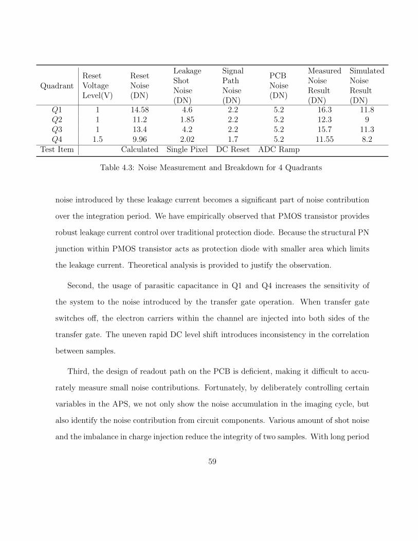
QuadrantResetVoltageLevel(V)
ResetNoise(DN)
LeakageShotNoise(DN)
SignalPathNoise(DN)
PCBNoise(DN)
MeasuredNoiseResult(DN)
SimulatedNoiseResult(DN)
Q1 1 14.58 4.6 2.2 5.2 16.3 11.8Q2 1 11.2 1.85 2.2 5.2 12.3 9Q3 1 13.4 4.2 2.2 5.2 15.7 11.3Q4 1.5 9.96 2.02 1.7 5.2 11.55 8.2
Test Item Calculated Single Pixel DC Reset ADC Ramp
Table 4.3: Noise Measurement and Breakdown for 4 Quadrants
noise introduced by these leakage current becomes a significant part of noise contribution
over the integration period. We have empirically observed that PMOS transistor provides
robust leakage current control over traditional protection diode. Because the structural PN
junction within PMOS transistor acts as protection diode with smaller area which limits
the leakage current. Theoretical analysis is provided to justify the observation.
Second, the usage of parasitic capacitance in Q1 and Q4 increases the sensitivity of
the system to the noise introduced by the transfer gate operation. When transfer gate
switches off, the electron carriers within the channel are injected into both sides of the
transfer gate. The uneven rapid DC level shift introduces inconsistency in the correlation
between samples.
Third, the design of readout path on the PCB is deficient, making it difficult to accu-
rately measure small noise contributions. Fortunately, by deliberately controlling certain
variables in the APS, we not only show the noise accumulation in the imaging cycle, but
also identify the noise contribution from circuit components. Various amount of shot noise
and the imbalance in charge injection reduce the integrity of two samples. With long period
59

of separation between samples due to row operation, the correlation between the samples
is compromised.
4.5 Correlated Double Sampling
4T quadrants are designed to test the performance of CDS with parasitic capacitor versus
MIM capacitor with different transistor level variations. 4T Pixels output both reset level
and signal voltage during one normal imaging cycle while 3T pixels just read the same
voltage twice. After two reading are stored in memory, they are subtracted with each
other in pixel level, eliminating the reset level while keeping the signal collected by a-Se.
Noise measurements in Figure 4.13 indicate none of 4T quadrants matches the theo-
retical value. This mismatch motivates us to review the prerequisites and assumptions of
CDS. CDS subtracts two correlated samples to achieve the reduction of KTC reset noise,
1/f noise and DC offset. First, the samples for subtraction must be correlated. To ensure
strong correlation, samples are usually taken quickly by a sample and hold circuit, such
as the one shown in Figure 4.14. By operating the gates with appropriate timing, we can
store the reset value of the pixel in Cs and photon signal plus reset value in Cr as quickly
as possible. Then a differential amplifier performs the subtraction and produces the CDS
result with one readout.
To compare the noise performance for these APS configurations with different gain, we
can calculate SNR at the system output. Assuming a-Se is exposed to X-ray and generates
1000 e− into the pixels in 40 ms integration period with 1V reset voltage, SNR can be
60
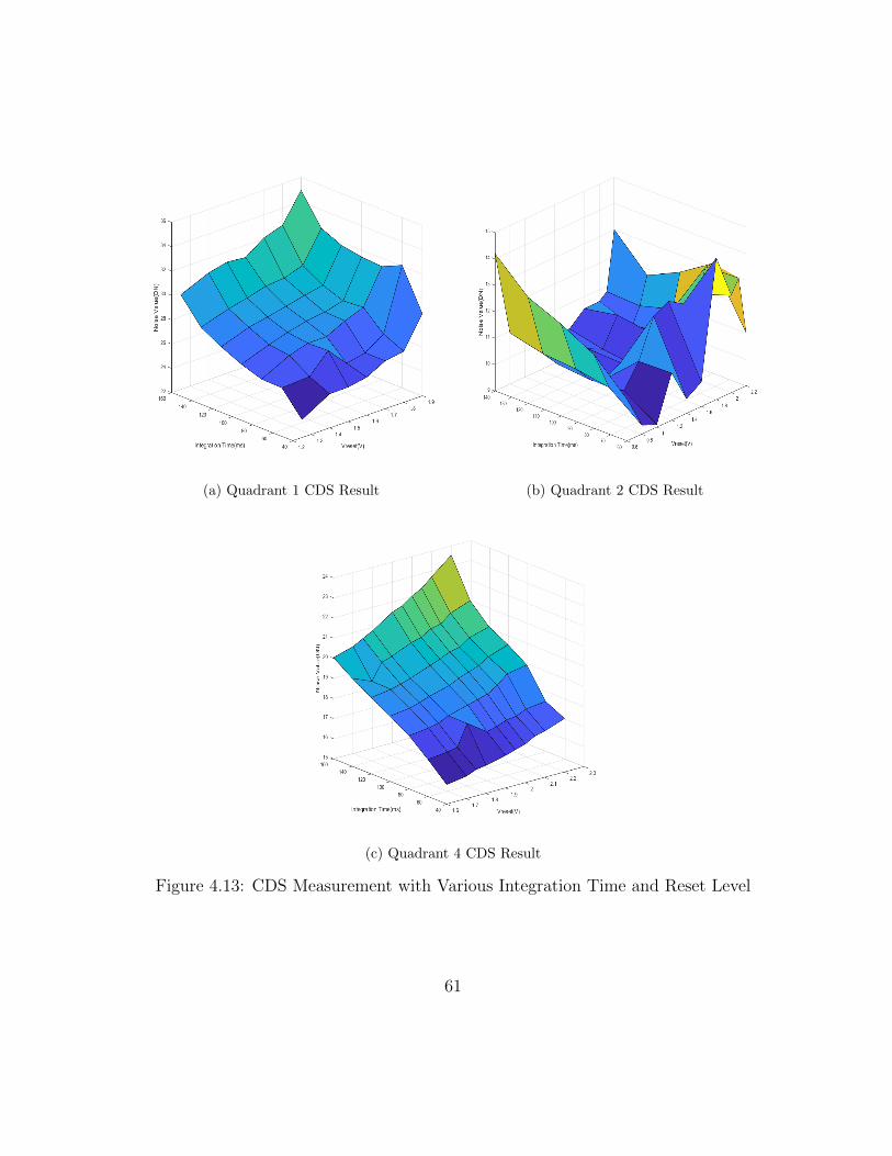
(a) Quadrant 1 CDS Result (b) Quadrant 2 CDS Result
(c) Quadrant 4 CDS Result
Figure 4.13: CDS Measurement with Various Integration Time and Reset Level
61
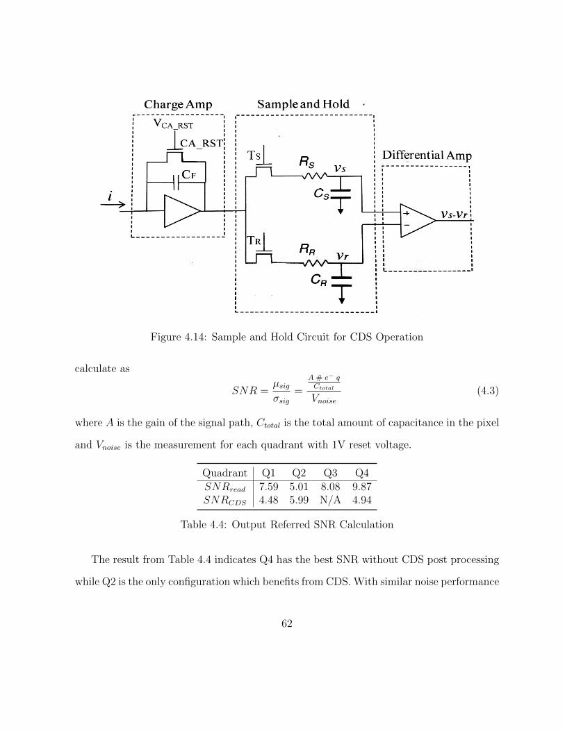
Figure 4.14: Sample and Hold Circuit for CDS Operation
calculate as
SNR =µsig
σsig=
A # e− qCtotal
Vnoise(4.3)
where A is the gain of the signal path, Ctotal is the total amount of capacitance in the pixel
and Vnoise is the measurement for each quadrant with 1V reset voltage.
Quadrant Q1 Q2 Q3 Q4SNRread 7.59 5.01 8.08 9.87SNRCDS 4.48 5.99 N/A 4.94
Table 4.4: Output Referred SNR Calculation
The result from Table 4.4 indicates Q4 has the best SNR without CDS post processing
while Q2 is the only configuration which benefits from CDS. With similar noise performance
62
to Q1, Q4 has higher conversion gain in the pixel level which results better SNR without
CDS processing. Q2 has the best correlation between samples, resulting a reduction of
noise value after CDS calculation.
In our design, we only have one unity gain amplifier and the transfer signal is a row-base
signal. Therefore, the minimum time to sample one pixel twice is one row readout, which
is about 156 µs. This largely reduces the correlation between samples suggested by [28].
In addition, different amount of leakage current going into sense node and integration node
during this time gap also reduces the effectiveness of CDS. This explains why the noise
value is always higher with longer integration time. Furthermore, two readouts onto the
PCB level for CDS subtraction results doubling not only the sampling noise but also the
noise along the signal path. Unfortunately, this signal path is proven to be problematic
in Chapter 4.3. Due to the variations among the quadrants, we find Q2 benefits from
CDS. First, transfer gate in Q2 employs transmission gate, where the charges released by
one switch are absorbed by the complementary device. With one MIM capacitor in each
side of the transfer gate, the charge is equally redistributed to the drain and the source.
Leakage current to both nodes are more likely to be identical because the source of leakage
is located between these two MIN capacitors. Both factors reduce the difference between
samples, which consequently benefits to CDS noise reduction as shown in [29].
For effective CDS, the time gap between two sampling actions should be adjusted such
that two samples are acquired within a very small time frame. This can be achieved by
replacing the row transfer gate signal to a shift register. Only minimum delay should be
placed between samples for complete charge transfer and ADC operation. On pixel level,
using transmission gate between integration and sense node is recommended to counter
63
excessive charge injection and imbalanced leakage current from an explicit protection diode.
With proper sizing of the NMOS and PMOS transistor in the transmission gate, the charge
carrier that injects to the drain and source can be canceled which maintains the voltage
level even for small capacitance nodes in the pixel.
4.6 Summary
In this chapter, we first analyzes leakage current through protection diode to the sense
node and integration node of Q1. Then we applies similar experiment to estimate the
leakage current of other quadrants to calculate the associated shot noise. Next, the signal
path noise is characterized and modeled as a linear function with pixel voltage output as
variable. It is higher than the design specification and the cause analysis is conducted
in the next chapter. Last, we examine the noise performance of all the quadrants and
compare them with simulation results. We predict the trend of noise value due to leakage
and explain the discrepancy as dealing with imperfect design. Measurements at high reset
voltage level exhibit valid half reset noise at sub-threshold region for all quadrants even
with noisy readout path.
64

Chapter 5
PCB Design Review
PCB design exhibits some issues which prevent the chip from achieving the theoretical noise
performance. Some problems can be fixed or diminished by board level modifications. In
this chapter, we focus on the solving the issues identified in the previous chapter.
5.1 ADC Layout
As the resolution of imager increases dramatically in recent years, readout speed usually
limits the maximum frame rate of the imager. Therefore, high speed ADC is employed
to digitize the analog voltage signal from pixel outputs. High speed ADC circuitry is
always a challenging design and its performance is extremely crucial. To characterize noise
performance of the imager, ADC’s noise value should theoretically be at least 10 times less
than the imager. In our case, we use a 16-bit SAR ADC with a 3.3 V reference voltage.
Noise performance according to the data sheet is half of one LSB which is about 50 µV .
65
To achieve such noise level, ADC and the supporting circuit must be set up properly as
suggested by the evaluation document. However, our design did not follow the same path
on the layout, which is proven to degrade the performance of the system.
To validate the DC performance of the ADC, we can simply bypass the pixel output and
apply a constant DC voltage at the input of the low pass filter. To be certain, we use two
test sources: one power supply with a few decoupling capacitors connected between two
terminals and a 1.5 V AA battery to eliminate the 60 Hz noise coupled from the ac outlet.
In addition, we also disable the digital control signals going into the chip to provide a quiet
environment. The results from both sources at different sampling frequencies indicate that
the noise value is at least 3.5 DN which is much bigger than stated value in the data sheet.
As shown in Figure 5.1, there is a bump at 3.6 KHz, yet the overall noise floor is still too
high to be 1 DN over the frequency range.
Figure 5.1: ADC Noise PSD from Battery
66
Next, we need to verify the effective resolution of ADC by applying a slow voltage ramp.
In theory, as long as the sampling frequency is fast enough, binary outputs should cover
all possible bits with no missing codes. However, the test result shown in 5.2 indicates
the ADC clearly suffers from missing code error. The red line is the average of 500 ramp
up signal from the same pixel while the blue line is a sample record out at the 500 second.
First, we see the reading bounces up and down between 60-th sample and 90-th sample,
which is a typical noise behavior from an ADC. Then, the straight line between 30-th
sample and 60-th sample is called “stuck” bits, which remains as the same code repeated
many times even if the input has changed. The reasons for these “stuck” bits are the size
and placement of the reference capacitor, insufficient drive strength of the reference voltage
buffer, or poor selection of the reference. These would result in excess noise [30].
Figure 5.2: ADC Output from Ramping Signal
To elaborate this issue, Figure 5.3 shows the histogram of the last 5 bits of ADC output.
67

For DC test input, there should be a normal distribution centered at 20 DN. However, since
the ADC cannot output 20 DN, the digital code stuck between 14 DN and 29 DN .
Figure 5.3: Histogram of Last 5 bits of ADC Output
Due to excessive high noise behavior of the ADC, we need to review the setup of
ADC from both layout and timing perspective. The ground truth setup is given in the
device evaluation data sheet [31], serving as the reference for our layout. The evaluation
setup emphasizes the separation of digital and analog signals. It is because the digital
signal operates at high speed and strong drive strength, resulting in strong interfere from
the analog signal path. Yet in our design, we have two instances that the Clock trace and
Converse trace from FPGA cross the analog interface of ADC as highlighted in Figure 5.4a.
Two digital signals overlap the reference voltage pin and positive input pin which are
the most crucial analog input of ADC. ADC data sheet illustrates the layout as shown
68
(a) Digital Singal CLK Crossing ADC (b) Reference Voltage Layout
(c) Recommand ADC Layout
Figure 5.4: ADC Layout Issues
69

(a) Analog Signal with Clock On (b) Analog Signal with Clock Off
Figure 5.5: Oscilloscope Screen Shot Comparison with Clock Signal Disable during Con-version
in Figure 5.4c, suggesting the analog and digital interface should be isolated as far as
possible. The data sheet recommends to place both the reference voltage component and
the decoupling capacitor right underneath the device as illustrated in Figure 5.4b. However,
they are routed far away from the ADC, which makes the decoupling capacitor ineffective.
This distance allows unwanted signal to interfere with the reference voltage, resulting a
noisy reference for the ADC. Once an incorrect bit decision has been made, ADC fills the
remaining bits with ones or zeros, which presents as stuck bits issue in Figure 5.2.
In addition, we can see that the Clock signal interfere with the input of ADC by probing
both signals with an oscilloscope. In Figure 5.5a, the digital signals below are Convert,
ADC output and Clock signal, respectively. The yellow analog signal is probed at the input
of low-pass filter and the green signal is the input of ADC. We can see the low-pass filter
fails to filter out the high frequency Clock interference, and the interference becomes more
severe at the input of ADC. This suggests the interference occurs locally near the ADC as
presented in [32]. In Figure 5.5b, we manage to turn off the Clock signal during analog
70

conversion to provide a quiet environment. It is visually impressive to see the input signal
becomes much less noisy. However, the outcomes indicate that there is little improvement
on noise value, suggesting the impact of Clock interference is reduced but it is not the
biggest noise contributor here.
5.2 Component Selection
One of the most severe issues on noise performance is the deterministic sinusoidal-like ef-
fect during sampling phase as mentioned in Chapter 4.2. We suspect that it is caused by
component selection for supportive circuit on PCB level. Therefore, a series of investiga-
tions are performed to validate this hypothesis. On PCB schematic, it is easy to find that
all supportive circuits employ LT1498 OPAMP as voltage sources for the imager, such as
analog Vdd, digital Vdd and the reset voltages for all quadrants. The purpose is to keep
the circuit structure as simple as possible to ease the debugging process. As we look into
the detail on data sheet [33], we found that the OPAMP remains stable while driving ca-
pacitive loads up to 100nF. However, 100nF is small compare to the power loading of the
imager and all decoupling capacitors. However, decoupling capacitors as large as 5.6 µF
are placed in the circuit regardlessly, which poses a potential stability issue to the system.
Ideally, voltage source should be provided by low-dropout (LDO) regulator which en-
sures enough output power for driving the imager. In additional, LDO is great for noise
isolation because the bandgap reference can provide a stable signal output despite changes
in input. The difficulty of board modification is due to the incompatibility of the footprint.
It is because each LT1498 provides two adjustable outputs while LDO only has one. If we
71
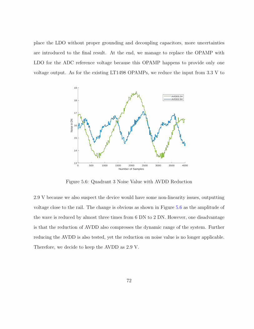
place the LDO without proper grounding and decoupling capacitors, more uncertainties
are introduced to the final result. At the end, we manage to replace the OPAMP with
LDO for the ADC reference voltage because this OPAMP happens to provide only one
voltage output. As for the existing LT1498 OPAMPs, we reduce the input from 3.3 V to
0 500 1000 1500 2000 2500 3000 3500 4000
Number of Samples
13
14
15
16
17
18
19
Noi
se in
DN
AVDD3.3VAVDD2.9V
Figure 5.6: Quadrant 3 Noise Value with AVDD Reduction
2.9 V because we also suspect the device would have some non-linearity issues, outputting
voltage close to the rail. The change is obvious as shown in Figure 5.6 as the amplitude of
the wave is reduced by almost three times from 6 DN to 2 DN. However, one disadvantage
is that the reduction of AVDD also compresses the dynamic range of the system. Further
reducing the AVDD is also tested, yet the reduction on noise value is no longer applicable.
Therefore, we decide to keep the AVDD as 2.9 V.
72

5.3 Grounding Scheme
In mixed-signal chip, maintaining wide dynamic range with low noise in hostile digital
environments is dependent upon using good high-speed circuit design techniques including
proper signal routing, decoupling, and grounding. The ground plane not only acts as a
low impedance return path for decoupling high frequency currents (caused by fast digital
logic) but also minimizes EMI/RFI emissions. Because of the shielding action of the ground
plane, the circuit’s susceptibility to external EMI/RFI is also reduced as mentioned in [34].
The ground return wire inductance and resistance is shared between the analog and digital
circuits, and this is what causes the interaction and error. The fundamental concept of
single-point ground system is to make the digital return current path flow directly to the
GND REF as shown in Figure 5.7. As for our mixed-signal imager, it is highly desirable to
physically separate sensitive analog components from digital components. To achieve that,
the original back plane of the PCB are cut so that it separates into two isolated planes, the
analog ground and digital ground. Then two sections are connected back together at the
power supply connector. However, due to inexperience, the designer placed the location of
connector such that the digital return signal generated from blue boxes are allowed to go
through the analog ground following the red arrows as shown in Figure 5.8. The mistake we
made in this PCB layout is exactly like the incorrect example in Figure 5.7 about different
frequencies of return signals sharing the same return path. The better solution for the
connector is to place a few of them on the right side of the blue box where minimizes the
length of return path and the number of affected components.
Another issue about this PCB is the location of decoupling capacitors. Ideally, Each
73
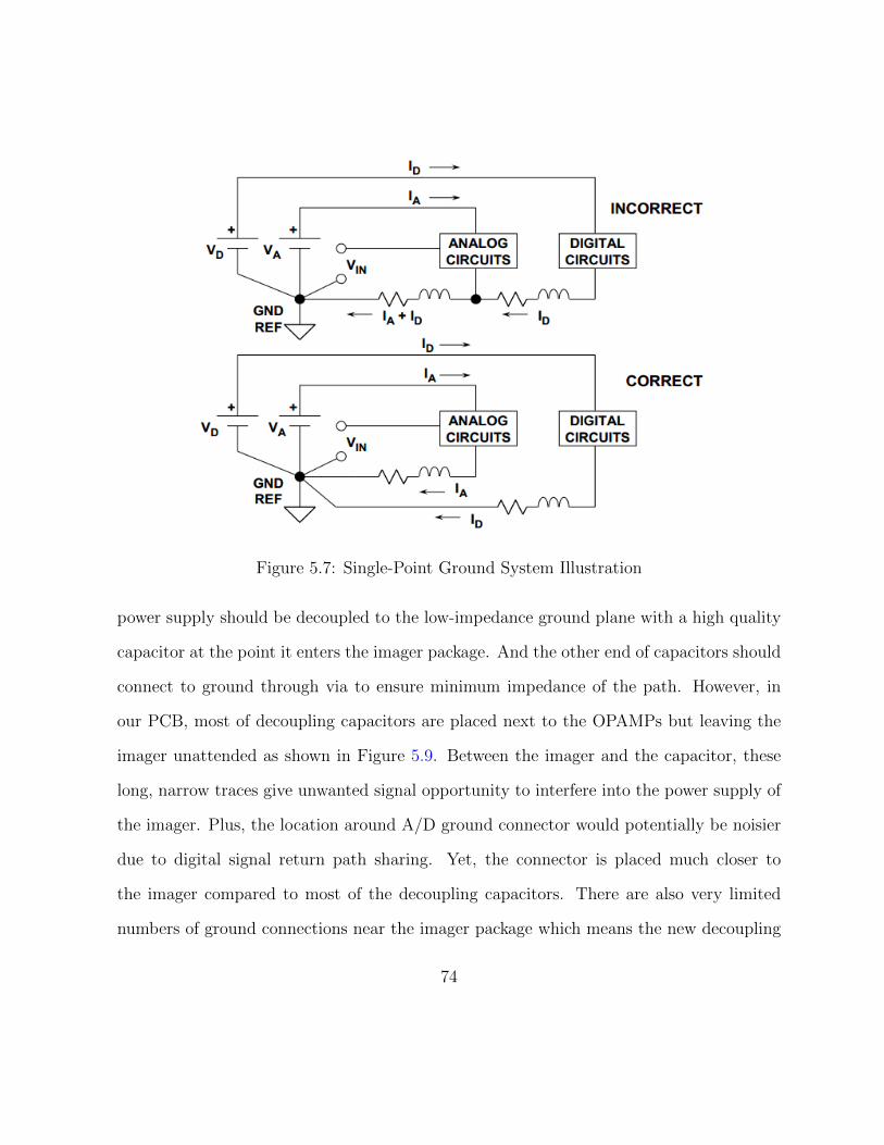
Figure 5.7: Single-Point Ground System Illustration
power supply should be decoupled to the low-impedance ground plane with a high quality
capacitor at the point it enters the imager package. And the other end of capacitors should
connect to ground through via to ensure minimum impedance of the path. However, in
our PCB, most of decoupling capacitors are placed next to the OPAMPs but leaving the
imager unattended as shown in Figure 5.9. Between the imager and the capacitor, these
long, narrow traces give unwanted signal opportunity to interfere into the power supply of
the imager. Plus, the location around A/D ground connector would potentially be noisier
due to digital signal return path sharing. Yet, the connector is placed much closer to
the imager compared to most of the decoupling capacitors. There are also very limited
numbers of ground connections near the imager package which means the new decoupling
74
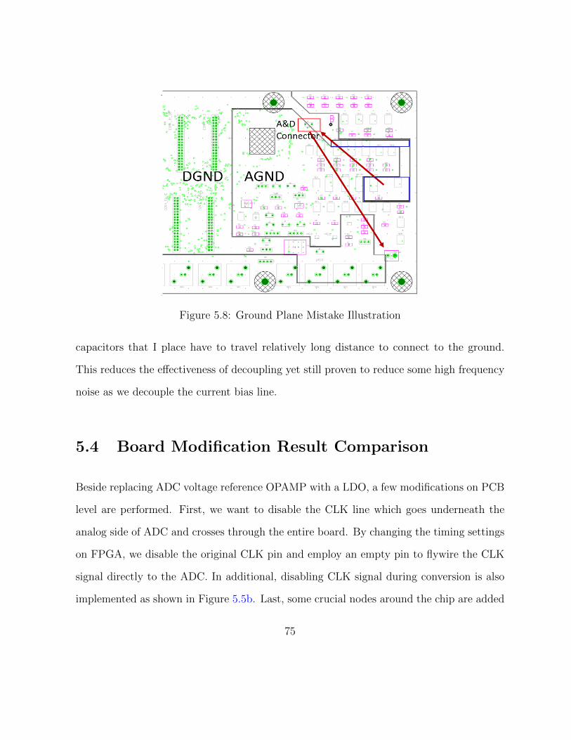
Figure 5.8: Ground Plane Mistake Illustration
capacitors that I place have to travel relatively long distance to connect to the ground.
This reduces the effectiveness of decoupling yet still proven to reduce some high frequency
noise as we decouple the current bias line.
5.4 Board Modification Result Comparison
Beside replacing ADC voltage reference OPAMP with a LDO, a few modifications on PCB
level are performed. First, we want to disable the CLK line which goes underneath the
analog side of ADC and crosses through the entire board. By changing the timing settings
on FPGA, we disable the original CLK pin and employ an empty pin to flywire the CLK
signal directly to the ADC. In additional, disabling CLK signal during conversion is also
implemented as shown in Figure 5.5b. Last, some crucial nodes around the chip are added
75
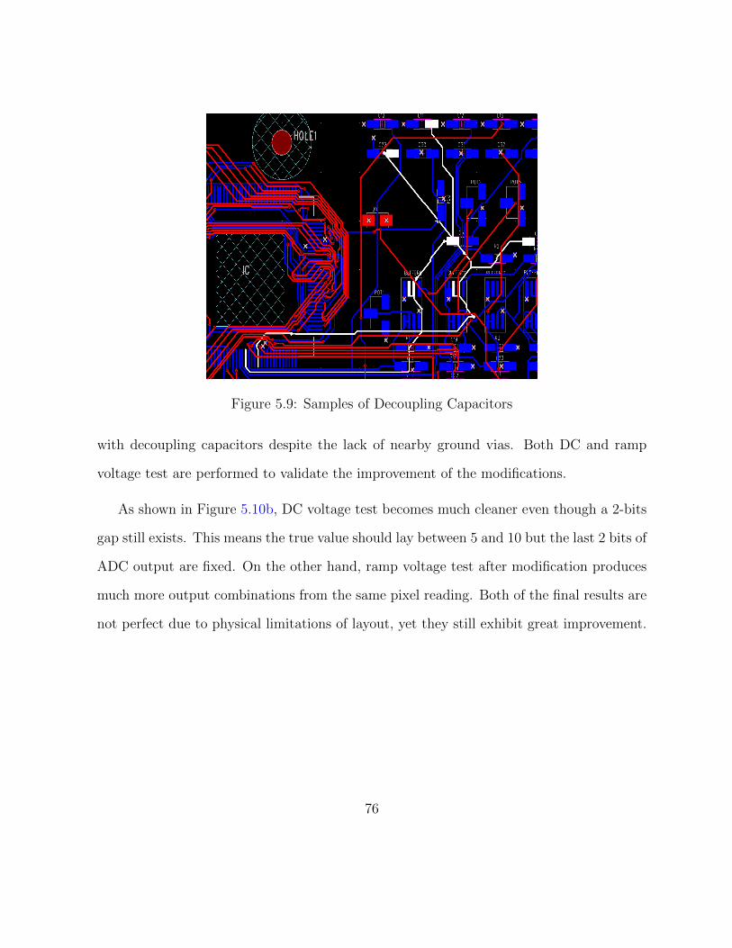
Figure 5.9: Samples of Decoupling Capacitors
with decoupling capacitors despite the lack of nearby ground vias. Both DC and ramp
voltage test are performed to validate the improvement of the modifications.
As shown in Figure 5.10b, DC voltage test becomes much cleaner even though a 2-bits
gap still exists. This means the true value should lay between 5 and 10 but the last 2 bits of
ADC output are fixed. On the other hand, ramp voltage test after modification produces
much more output combinations from the same pixel reading. Both of the final results are
not perfect due to physical limitations of layout, yet they still exhibit great improvement.
76
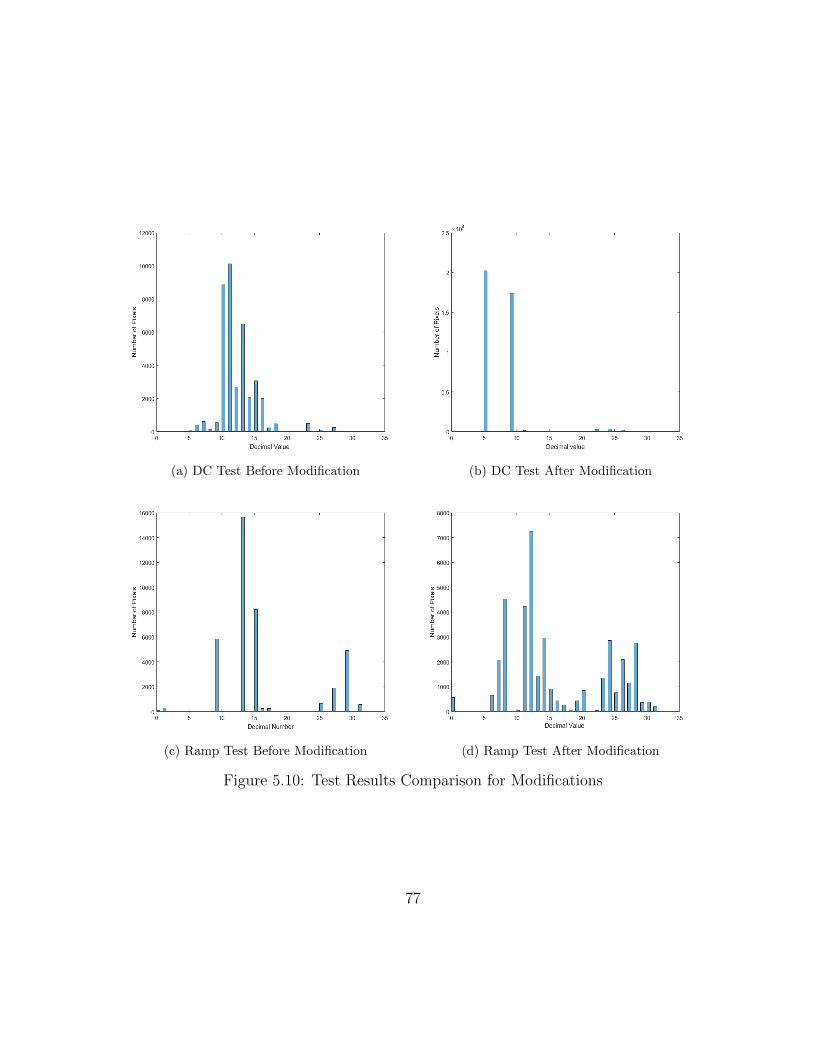
(a) DC Test Before Modification (b) DC Test After Modification
(c) Ramp Test Before Modification (d) Ramp Test After Modification
Figure 5.10: Test Results Comparison for Modifications
77


Chapter 6
Conclusion and Future Work
We have identified and characterized a number of issues that have degraded the perfor-
mance of the X-ray imaging system, and characterized them. The system suffers from
unexpectedly high noise level, which we believe arises from the leakage current, the im-
proper usage of parasitic capacitor and the deficient design of readout path. Furthermore,
the improvement introduced by CDS is only limited to Q2 because of the shot noise and
the imbalance in charge injection. We have several recommendations for future fabrication,
including redesigning the readout path, replacing protection diode with proper transmis-
sion gate and adding some stand-alone test pixels. The suggested revisions are expected
to partially resolve the degradation, resulting in SNRs of 13, whereas in conventional use
the present system gives an SNR around 5.2, which is too low to be useful. As an interim
measure, we have applied modifications on PCB level and operational timing to optimize
the usage of the present system to the point that the device can now obtain images with
an SNR of 9.87. These optimization enables the X-ray imager to capture phase contract
79
information from an object with a thickness of 60 µm.
In future, there are some approaches to achieve better noise performance of this im-
ager. The first approach is to redesign the readout path on PCB. With careful selection
and placement of electronic components, stable low-noise peripheral supportive circuity is
needed for noise characterization. Best practice on PCB layout is as important as designing
the imager. In addition, the required time and cost to remake the PCB is substantially
lower than redesigning the imager IC.
For more effective CDS in system level, timing between two samplings should be reduced
to ensure correlation. This can be achieved by replacing the row transfer gate signal to a
shift register. Only a minimum delay would be introduced between sampling for complete
charge transfer and ADC operation. On pixel level, using proper sizing transmission gate
is recommended to counter charge injection and leakage current.
Last but not the least, some stand-alone test pixels for each APS configuration with
direct access are recommended to be placed aside from the imager array. They can be
used to characterize leakage current and parasitic capacitance with more aggressive tests
without damaging the main array.
80

References
[1] P. J. Mohr and B. N. Taylor, “CODATA recommended values of the fundamental
physical constants: 1998,” Reviews of Modern Physics, vol. 72, pp. 351–495, 2000.
[2] F. Hippert, Neutron and X-ray Spectroscopy. Collection Grenoble Sciences. Springer,
2006.
[3] G. Whitman and T. Haygood, Digital Mammography: A Practical Approach, Cam-
bridge medicine. Cambridge University Press, 2012.
[4] M. Overdick, C. Baumer, J. Engel, C. Herrmann, H. Kruger, M. Simon, R. Steadman,
and G. Zeitler, “Status of direct conversion detectors for medical imaging with X-
rays,” IEEE Transactions on Nuclear Science, vol. 56, no. 4, pp. 1800–1809, 2009.
[5] D. Litwiller, “CCD vs. CMOS,” Photonics Spectra, vol. 35, no. 1, pp. 154–158, 2001.
[6] G. C. Holst and T. S. Lomheim, CMOS/CCD sensors and camera systems. JCD
Publishing USA, 2007.
81

[7] A. Parsafar, C. Scott, A. El-Falou, P. M. Levine, and K. S. Karim, “Direct-conversion
CMOS X-ray imager with with 5.6 µm ×6.25 µm pixels,” IEEE Electron Device
Letters, vol. 36, pp. 481–483, 2015.
[8] G. Hajdok, J. Battista, and I. Cunningham, “Fundamental X-ray interaction limits in
diagnostic imaging detectors: Spatial resolution,” Medical Physics, vol. 35, no. 7, pp.
3180–3193, 2008.
[9] A. Parsafar, “Design and Implementation of a High Resolution CMOS X-Ray Imager
with Amorphous Selenium Sensor,” University of Waterloo, 2015.
[10] V. Ambegaokar and B. Halperin, “Voltage due to thermal noise in the dc josephson
effect,” Physical Review Letters, vol. 22, no. 25, p. 1364, 1969.
[11] Y. M. Blanter and M. Buttiker, “Shot noise in mesoscopic conductors,” Physics Re-
ports, vol. 336, no. 1-2, pp. 1–166, 2000.
[12] J. Chang, A. Abidi, and C. Viswanathan, “Flicker noise in CMOS transistors from
subthreshold to strong inversion at various temperatures,” IEEE Transactions on
Electron Devices, vol. 41, no. 11, pp. 1965–1971, 1994.
[13] K. K. Hung, P. K. Ko, C. Hu, and Y. C. Cheng, “A unified model for the flicker noise
in metal-oxide-semiconductor field-effect transistors,” IEEE Transactions on Electron
Devices, vol. 37, no. 3, pp. 654–665, 1990.
[14] A. V. D. Ziel, Noise in Solid State Devices and Circuits. Wiley, 1986.
[15] H. Tian and A. El Gamal, “Analysis of 1/f noise in CMOS APS,” Proc.SPIE, vol.
3965, pp. 3965 – 3965 – 9, 2000.
82
[16] P. R. Gray, P. Hurst, R. G. Meyer, and S. Lewis, Analysis and design of analog
integrated circuits. Wiley, 2001.
[17] D. J. Eisenstein and W. Hu, “Baryonic features in the matter transfer function,” The
Astrophysical Journal, vol. 496, no. 2, pp. 605–625, 1998.
[18] R. Senthinathan and J. Prince, “Simultaneous switching ground noise calculation for
packaged CMOS devices,” IEEE Journal of Solid-State Circuits, vol. 26, no. 11, pp.
1724–1728, 1991.
[19] P. E. Debevec and J. Malik, “Recovering high dynamic range radiance maps from
photographs,” Proceedings of the 24th annual conference on Computer graphics and
interactive techniques, pp. 369–378, 1997.
[20] S. Decker, D. McGrath, K. Brehmer, and C. G. Sodini, “A 256/spl times/256 CMOS
imaging array with wide dynamic range pixels and column-parallel digital output,”
IEEE Journal of Solid-state Circuits, vol. 33, no. 12, pp. 2081–2091, 1998.
[21] H. Tian, B. Fowler, and A. E. Gamal, “Analysis of temporal noise in CMOS photo-
diode active pixel sensor,” IEEE Journal of Solid-state Circuits, vol. 36, no. 1, pp.
92–101, 2001.
[22] B. Pain, G. Yang, M. Ortiz, C. Wrigley, B. Hancock, and T. Cunningham, “Analy-
sis and enhancement of low-light-level performance of photodiode-type CMOS active
pixel images operated with sub-threshold reset,” Jet Propulsion LaboratonJ, Califor-
nia Institute of Technology, 2000.
83

[23] E. R. Fossum et al., “Charge transfer noise and lag in CMOS active pixel sensors,”
Proc. IEEE Workshop on CCDs and Advanced Image Sensors, pp. 11–13, 2003.
[24] N. Teranishi, “Analysis of subthreshold current reset noise in image sensors,” Sensors,
vol. 16, no. 5, pp. 663–688, 2016.
[25] A. El Gamal and H. Eltoukhy, “CMOS image sensors,” IEEE Circuits and Devices
Magazine, vol. 21, no. 3, pp. 6–20, 2005.
[26] H. Wey and W. Guggenbuhl, “An improved correlated double sampling circuit for low
noise charge coupled devices,” IEEE transactions on Circuits and Systems, vol. 37,
no. 12, pp. 1559–1565, 1990.
[27] S. G. Narendra and A. P. Chandrakasan, Leakage in nanometer CMOS technologies.
Springer Science Business Media, 2006.
[28] M. Tabet, Double sampling techniques for CMOS image sensors. University of Wa-
terloo Department of Electrical and Computer Engineering, 2002.
[29] C. C. Enz and G. C. Temes, “Circuit techniques for reducing the effects of op-amp
imperfections: autozeroing, correlated double sampling, and chopper stabilization,”
Proceedings of the IEEE, vol. 84, no. 11, pp. 1584–1614, 1996.
[30] A. Walsh, “Voltage reference design for precision successive approximation adcs,”
Transactions on Electrical and Electronic Engineering, vol. 47, no. 11, pp. 440–448,
2013.
[31] T. Matsuura, “Recent progress on CMOS successive approximation ADCs,” Circuits
and Devices Magazine, vol. 33, no. 11, pp. 1696–1701, 2009.
84

85
[32] L. S. Milor, “A tutorial introduction to research on analog and mixed-signal circuit
testing,” IEEE Transactions on Circuits and Systems II: Analog and Digital Signal
Processing, vol. 45, no. 10, pp. 1389–1407, 1998.
[33] Linear Technology, “10mhz, 6v/s, dual/quad rail-to-rail input and output precision
C-Load op amps,” [Online]. Available: http://www.analog.com/media/en/technical-
documentation/data-sheets/14989fg.pdf, 2010.
[34] J. B. Walt Kester and M. Byrne, “Grounding data converters and solving the mystery
of AGND and DGND,” Analog Devices, 2009.
[35] N. Teranishi and N. Mutoh, “Partition noise in CCD signal detection,” IEEE Trans-
actions on Electron Devices, vol. 33, no. 11, pp. 1696–1701, 1986.
[36] E. R. Fossum, D. B. Hondongwa et al., “A review of the pinned photodiode for CCD
and CMOS image sensors,” IEEE J. Electron Devices Soc., vol. 2, no. 3, pp. 33–43,
2014.
[37] D. M. Chandler and S. S. Hemami, “VSNR: A wavelet-based visual signal-to-noise
ratio for natural images,” IEEE Transactions on Image Processing, vol. 16, no. 9, pp.
2284–2298, 2007.