norhayati soin 06 keee 4426 week 14/2 31/03/2006 chapter 6 semiconductor memories
TRANSCRIPT
Norhayati Soin 06 KEEE 4426 WEEK 142 31032006
CHAPTER 6
Semiconductor Memories
Norhayati Soin 06 KEEE 4426 WEEK 142 31032006
INTRODUCTIONMemory circuits provide the means of storing information (data) on a temporary or permanent basis and for future recalls
Magnetic memoryGenerally is capable of storing large amount of data at very low cost but the access time (the time it takes to locate and then read or write) is usually very long
Semiconductor memoriesuse electrical signals to identify memory location and its content The access time in several orders of magnitude faster that magnetic memory
MOS and bipolar technologies can be used to implement various
types of semiconductor memories
Norhayati Soin 06 KEEE 4426 WEEK 142 31032006
CLASSIFICATION OF SEMICONDUCTOR MEMORIES
Semiconductor memories
volatile Non-volatile
loose their data once the power
supply is turned off
SRAM DRAM ROM EPROM
can retain their data even after power is removed
Norhayati Soin 06 KEEE 4426 WEEK 142 31032006
STATIC RAM (SRAM)
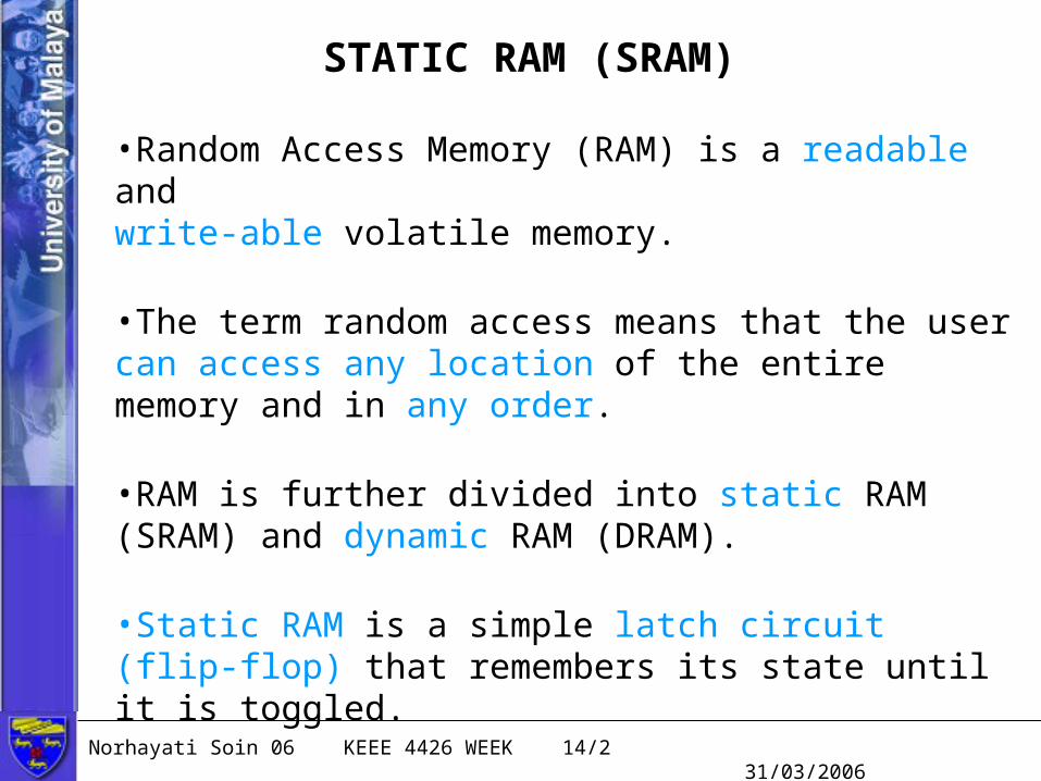
bullRandom Access Memory (RAM) is a readable andwrite-able volatile memory
bullThe term random access means that the user can access any location of the entire memory and in any order
bullRAM is further divided into static RAM (SRAM) and dynamic RAM (DRAM)
bullStatic RAM is a simple latch circuit (flip-flop) that remembers its state until it is toggled
Norhayati Soin 06 KEEE 4426 WEEK 142 31032006
STATIC RAM (SRAM)
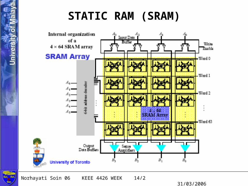
The simplest SRAM would be a simple data latch withpass transistors for selection and isolation
The actual implementation is usually carried out by the6-transistor cell
Norhayati Soin 06 KEEE 4426 WEEK 142 31032006
STATIC RAM (SRAM)
Norhayati Soin 06 KEEE 4426 WEEK 142 31032006
STATIC RAM (SRAM)
Norhayati Soin 06 KEEE 4426 WEEK 142 31032006
DYNAMIC RAM (DRAM)
Fabricated using MOS technology and are noted for their high capacity low power requirement and moderate operating speed (when compared to SRAM)
DRAMs make use of MOS capacitors to store the data as electronic charges The capacitors can be switched in and out of the bit lines via a pass transistor
The storage capacitor will loose its charge over time Therefore DRAMs must be refreshed in a regular basis
Norhayati Soin 06 KEEE 4426 WEEK 142 31032006
DYNAMIC RAM (DRAM)
The read operation for DRAM is a destructive process
Therefore extra peripheral circuits must be used to rewritethe DRAM cells as soon as it is read
These operations are incorporated as part of the DRAM chip and are transparent to the users
The memory organization can be similar to the SRAM array However the memory size for DRAMs is usually much larger
Currently DRAM in 1G-bit size are available while SRAM sizes of under a 1M-bit are more common
Norhayati Soin 06 KEEE 4426 WEEK 142 31032006
DYNAMIC RAM (DRAM)
The most important difference of the DRAM fabrication process from other technology is the storage capacitor
The single-transistor DRAM cell requires a capacitor that can store sufficient charge to allow the cell state to state true between refresh cycles
The most significant development in the DRAM devices has been the advance in the capacitor design
Norhayati Soin 06 KEEE 4426 WEEK 142 31032006
DYNAMIC RAM (DRAM)
For a minimum Tox the remaining adjustable parameters are εi and A
The DRAM capacitors have been improved in two ways increasing the surface area and increasing the capacitor dielectric constant
Norhayati Soin 06 KEEE 4426 WEEK 142 31032006
Trenched DRAM CellbullOne area of progress in making a capacitor with a larger surface area is to form the capacitor in a trench
bullThis technique make use of a deep trench (gt 7μm into the silicon)
bullIt has the advantage of allowing the transistors to be formed nearly planaron the surface with the trench extendingbelow the device active area
Norhayati Soin 06 KEEE 4426 WEEK 142 31032006
Trenched DRAM Cell
Fabrication results of Trenched DRAM Cell
The effect of the large surface area and the ability to thin the gate dielectric by improving the reliability of the thin oxides has resulted in a DRAM that can store more charge in smaller top surface area
Norhayati Soin 06 KEEE 4426 WEEK 142 31032006
Stacked DRAM CellAnother area of tremendous progress in DRAM technology goes in the other direction and forms the capacitors in geometries that extend above the silicon to create a large capacitor area
The large surface areas can be created using a large planar capacitor shaped like a dome or a crown
These structures also take advantage of higher-dielectric constantmaterials for the inter-level dielectric for the capacitors mdash Ta2O5 (Ba Sr)TiO3 etc
Norhayati Soin 06 KEEE 4426 WEEK 142 31032006
Stacked DRAM Cell
Norhayati Soin 06 KEEE 4426 WEEK 142 31032006
Trench Cell vs Stacked Cell
Norhayati Soin 06 KEEE 4426 WEEK 142 31032006
Trench Cell vs Stacked CellIn the trench technology the cell process is completed before the gate oxidation Therefore there is no thermal process due to cell capacitor formation after the MOSFET formation
Another advantage in the trench cell is that there is no height difference between cell array region and peripheral circuit region
In the stacked cell the height difference require high aspect ratio contact holes and difficulty in the planarization process after the cell formation
The MOSFET formation steps are followed by the stacked capacitor formation steps
Norhayati Soin 06 KEEE 4426 WEEK 142 31032006
Trench Cell vs Stacked CellThese include high temperature processing steps suchas storage node insulator (SiO2SiN) formation SiN deposition for the self-aligned contact formation etc
Salicide (Self Aligned siLICIDE) process for the source and drain of the MOSFETs should be carefully designed to endure the high temperature process steps
For applications requiring Embedded DRAM trenched cell is more attractive because the DRAM cells are formed before the MOSFETs and because there is little height difference between the cell array and other regions on the chip
Norhayati Soin 06 KEEE 4426 WEEK 142 31032006
READ ONLY MEMORY(ROM)Certain applications may require the memory to hold data that are either permanent or will not be changed frequentlyIn this case nonvolatile memory is the candidate
As the name implies Read Only Memory (ROM) has noprovision to write or update its memory contents
The programming is usually done during the manufacturingprocess or by a burning procedure prior to field use
Norhayati Soin 06 KEEE 4426 WEEK 142 31032006
READ ONLY MEMORY
Norhayati Soin 06 KEEE 4426 WEEK 142 31032006
READ ONLY MEMORY
Norhayati Soin 06 KEEE 4426 WEEK 142 31032006
READ ONLY MEMORY
Norhayati Soin 06 KEEE 4426 WEEK 142 31032006
READ ONLY MEMORY
One obvious disadvantage of the mask ROM is the fact that a new photomask must be prepared if the stored data is to be changed
This will also be accompanied by a sizable turn-aroundtime when manufacturing the new ROMs
An alternate method of implementing the ROM is with a programmable technology such as fuse or anti-fuse
In this case the ROM becomes a programmable parts hence the name PROM
One advantage of the PROM is the fact that all ROMs regardless of data content can be manufactured using the same set of photomask and fabrication procedures
Norhayati Soin 06 KEEE 4426 WEEK 142 31032006
READ ONLY MEMORY
However a one-time-only programming procedure must be applied prior to field use After the PROM is programmed its contents cannot be changed anymore
Norhayati Soin 06 KEEE 4426 WEEK 142 31032006
READ ONLY MEMORYWhy EEPROMs
Field programmable capability to wireless portable telecommunication equipment
bull1048644 True 5V or lower operationbull1048644 Compatible with CMOSBiCMOS processesbull1048644 High operation speeds and high densitybull1048644 Key to embedded systemsbull1048644 Solid-state nonvolatile memoriesbull1048644 Multi-level Encoding
Norhayati Soin 06 KEEE 4426 WEEK 142 31032006
Conventional Flash E2PROM cell Structures
bullSimilar to an ordinary MOSFET except for an extra gate buried in the silicon dioxide
bullCharges are stored in the floating gate to alter the threshold voltage of the E2PROM cell
bullSimple construction and fabrication steps
bullVery high packing density
bullFlash E2PROM and E2PROMs bullshare the same technology
Norhayati Soin 06 KEEE 4426 WEEK 142 31032006
Flash E2PROM Cell Operations
bullFor programming hot electrons are created by thelarge drain bias current
bullThese electron tunnels through the thin gate oxide and become trapped in the floating gate
Norhayati Soin 06 KEEE 4426 WEEK 142 31032006
Limitations of Existing Flash E2PROM Cells
Most cells suffer from hole trapping in the thin gateoxide during erasing
Reduction in VTH window after several cycles of erase and programming
Norhayati Soin 06 KEEE 4426 WEEK 142 31032006
Memory Circuits
Semiconductor memories are comprised of a main storage array surrounded by peripheral circuits for read and write operations
These peripheral circuits includes row and columnaddress decoders data buffersregisters sense amplifiers and charge pumps circuits
The decoders and bufferregisters are basically digital circuits and can be implemented using conventional VLSI design methodology
The sense amplifier is basically a high gain circuit that is used to differentiate the stored information with a reference voltage
Norhayati Soin 06 KEEE 4426 WEEK 142 31032006
Memory Circuits
This is especially critical if the storage element is aDRAM cell
Most memory arrays require separate high and low voltage supply to operate
In order to eliminate the need for multiple external power supplies more memory chips have built-in charge pump circuits to generate multiple voltage levels from a single supply (usually 5V or 33V)
- CHAPTER 6
- INTRODUCTION
- CLASSIFICATION OF SEMICONDUCTOR MEMORIES
- STATIC RAM (SRAM)
- Slide 5
- Slide 6
- Slide 7
- DYNAMIC RAM (DRAM)
- Slide 9
- Slide 10
- Slide 11
- Trenched DRAM Cell
- Slide 13
- Stacked DRAM Cell
- Slide 15
- Trench Cell vs Stacked Cell
- Trench Cell vs Stacked Cell
- Slide 18
- READ ONLY MEMORY(ROM)
- READ ONLY MEMORY
- Slide 21
- Slide 22
- Slide 23
- Slide 24
- Slide 25
- Conventional Flash E2PROM cell Structures
- Flash E2PROM Cell Operations
- Limitations of Existing Flash E2PROM Cells
- Memory Circuits
- Slide 30
-

Norhayati Soin 06 KEEE 4426 WEEK 142 31032006
INTRODUCTIONMemory circuits provide the means of storing information (data) on a temporary or permanent basis and for future recalls
Magnetic memoryGenerally is capable of storing large amount of data at very low cost but the access time (the time it takes to locate and then read or write) is usually very long
Semiconductor memoriesuse electrical signals to identify memory location and its content The access time in several orders of magnitude faster that magnetic memory
MOS and bipolar technologies can be used to implement various
types of semiconductor memories
Norhayati Soin 06 KEEE 4426 WEEK 142 31032006
CLASSIFICATION OF SEMICONDUCTOR MEMORIES
Semiconductor memories
volatile Non-volatile
loose their data once the power
supply is turned off
SRAM DRAM ROM EPROM
can retain their data even after power is removed
Norhayati Soin 06 KEEE 4426 WEEK 142 31032006
STATIC RAM (SRAM)
bullRandom Access Memory (RAM) is a readable andwrite-able volatile memory
bullThe term random access means that the user can access any location of the entire memory and in any order
bullRAM is further divided into static RAM (SRAM) and dynamic RAM (DRAM)
bullStatic RAM is a simple latch circuit (flip-flop) that remembers its state until it is toggled
Norhayati Soin 06 KEEE 4426 WEEK 142 31032006
STATIC RAM (SRAM)
The simplest SRAM would be a simple data latch withpass transistors for selection and isolation
The actual implementation is usually carried out by the6-transistor cell
Norhayati Soin 06 KEEE 4426 WEEK 142 31032006
STATIC RAM (SRAM)
Norhayati Soin 06 KEEE 4426 WEEK 142 31032006
STATIC RAM (SRAM)
Norhayati Soin 06 KEEE 4426 WEEK 142 31032006
DYNAMIC RAM (DRAM)
Fabricated using MOS technology and are noted for their high capacity low power requirement and moderate operating speed (when compared to SRAM)
DRAMs make use of MOS capacitors to store the data as electronic charges The capacitors can be switched in and out of the bit lines via a pass transistor
The storage capacitor will loose its charge over time Therefore DRAMs must be refreshed in a regular basis
Norhayati Soin 06 KEEE 4426 WEEK 142 31032006
DYNAMIC RAM (DRAM)
The read operation for DRAM is a destructive process
Therefore extra peripheral circuits must be used to rewritethe DRAM cells as soon as it is read
These operations are incorporated as part of the DRAM chip and are transparent to the users
The memory organization can be similar to the SRAM array However the memory size for DRAMs is usually much larger
Currently DRAM in 1G-bit size are available while SRAM sizes of under a 1M-bit are more common
Norhayati Soin 06 KEEE 4426 WEEK 142 31032006
DYNAMIC RAM (DRAM)
The most important difference of the DRAM fabrication process from other technology is the storage capacitor
The single-transistor DRAM cell requires a capacitor that can store sufficient charge to allow the cell state to state true between refresh cycles
The most significant development in the DRAM devices has been the advance in the capacitor design
Norhayati Soin 06 KEEE 4426 WEEK 142 31032006
DYNAMIC RAM (DRAM)
For a minimum Tox the remaining adjustable parameters are εi and A
The DRAM capacitors have been improved in two ways increasing the surface area and increasing the capacitor dielectric constant
Norhayati Soin 06 KEEE 4426 WEEK 142 31032006
Trenched DRAM CellbullOne area of progress in making a capacitor with a larger surface area is to form the capacitor in a trench
bullThis technique make use of a deep trench (gt 7μm into the silicon)
bullIt has the advantage of allowing the transistors to be formed nearly planaron the surface with the trench extendingbelow the device active area
Norhayati Soin 06 KEEE 4426 WEEK 142 31032006
Trenched DRAM Cell
Fabrication results of Trenched DRAM Cell
The effect of the large surface area and the ability to thin the gate dielectric by improving the reliability of the thin oxides has resulted in a DRAM that can store more charge in smaller top surface area
Norhayati Soin 06 KEEE 4426 WEEK 142 31032006
Stacked DRAM CellAnother area of tremendous progress in DRAM technology goes in the other direction and forms the capacitors in geometries that extend above the silicon to create a large capacitor area
The large surface areas can be created using a large planar capacitor shaped like a dome or a crown
These structures also take advantage of higher-dielectric constantmaterials for the inter-level dielectric for the capacitors mdash Ta2O5 (Ba Sr)TiO3 etc
Norhayati Soin 06 KEEE 4426 WEEK 142 31032006
Stacked DRAM Cell
Norhayati Soin 06 KEEE 4426 WEEK 142 31032006
Trench Cell vs Stacked Cell
Norhayati Soin 06 KEEE 4426 WEEK 142 31032006
Trench Cell vs Stacked CellIn the trench technology the cell process is completed before the gate oxidation Therefore there is no thermal process due to cell capacitor formation after the MOSFET formation
Another advantage in the trench cell is that there is no height difference between cell array region and peripheral circuit region
In the stacked cell the height difference require high aspect ratio contact holes and difficulty in the planarization process after the cell formation
The MOSFET formation steps are followed by the stacked capacitor formation steps
Norhayati Soin 06 KEEE 4426 WEEK 142 31032006
Trench Cell vs Stacked CellThese include high temperature processing steps suchas storage node insulator (SiO2SiN) formation SiN deposition for the self-aligned contact formation etc
Salicide (Self Aligned siLICIDE) process for the source and drain of the MOSFETs should be carefully designed to endure the high temperature process steps
For applications requiring Embedded DRAM trenched cell is more attractive because the DRAM cells are formed before the MOSFETs and because there is little height difference between the cell array and other regions on the chip
Norhayati Soin 06 KEEE 4426 WEEK 142 31032006
READ ONLY MEMORY(ROM)Certain applications may require the memory to hold data that are either permanent or will not be changed frequentlyIn this case nonvolatile memory is the candidate
As the name implies Read Only Memory (ROM) has noprovision to write or update its memory contents
The programming is usually done during the manufacturingprocess or by a burning procedure prior to field use
Norhayati Soin 06 KEEE 4426 WEEK 142 31032006
READ ONLY MEMORY
Norhayati Soin 06 KEEE 4426 WEEK 142 31032006
READ ONLY MEMORY
Norhayati Soin 06 KEEE 4426 WEEK 142 31032006
READ ONLY MEMORY
Norhayati Soin 06 KEEE 4426 WEEK 142 31032006
READ ONLY MEMORY
One obvious disadvantage of the mask ROM is the fact that a new photomask must be prepared if the stored data is to be changed
This will also be accompanied by a sizable turn-aroundtime when manufacturing the new ROMs
An alternate method of implementing the ROM is with a programmable technology such as fuse or anti-fuse
In this case the ROM becomes a programmable parts hence the name PROM
One advantage of the PROM is the fact that all ROMs regardless of data content can be manufactured using the same set of photomask and fabrication procedures
Norhayati Soin 06 KEEE 4426 WEEK 142 31032006
READ ONLY MEMORY
However a one-time-only programming procedure must be applied prior to field use After the PROM is programmed its contents cannot be changed anymore
Norhayati Soin 06 KEEE 4426 WEEK 142 31032006
READ ONLY MEMORYWhy EEPROMs
Field programmable capability to wireless portable telecommunication equipment
bull1048644 True 5V or lower operationbull1048644 Compatible with CMOSBiCMOS processesbull1048644 High operation speeds and high densitybull1048644 Key to embedded systemsbull1048644 Solid-state nonvolatile memoriesbull1048644 Multi-level Encoding
Norhayati Soin 06 KEEE 4426 WEEK 142 31032006
Conventional Flash E2PROM cell Structures
bullSimilar to an ordinary MOSFET except for an extra gate buried in the silicon dioxide
bullCharges are stored in the floating gate to alter the threshold voltage of the E2PROM cell
bullSimple construction and fabrication steps
bullVery high packing density
bullFlash E2PROM and E2PROMs bullshare the same technology
Norhayati Soin 06 KEEE 4426 WEEK 142 31032006
Flash E2PROM Cell Operations
bullFor programming hot electrons are created by thelarge drain bias current
bullThese electron tunnels through the thin gate oxide and become trapped in the floating gate
Norhayati Soin 06 KEEE 4426 WEEK 142 31032006
Limitations of Existing Flash E2PROM Cells
Most cells suffer from hole trapping in the thin gateoxide during erasing
Reduction in VTH window after several cycles of erase and programming
Norhayati Soin 06 KEEE 4426 WEEK 142 31032006
Memory Circuits
Semiconductor memories are comprised of a main storage array surrounded by peripheral circuits for read and write operations
These peripheral circuits includes row and columnaddress decoders data buffersregisters sense amplifiers and charge pumps circuits
The decoders and bufferregisters are basically digital circuits and can be implemented using conventional VLSI design methodology
The sense amplifier is basically a high gain circuit that is used to differentiate the stored information with a reference voltage
Norhayati Soin 06 KEEE 4426 WEEK 142 31032006
Memory Circuits
This is especially critical if the storage element is aDRAM cell
Most memory arrays require separate high and low voltage supply to operate
In order to eliminate the need for multiple external power supplies more memory chips have built-in charge pump circuits to generate multiple voltage levels from a single supply (usually 5V or 33V)
- CHAPTER 6
- INTRODUCTION
- CLASSIFICATION OF SEMICONDUCTOR MEMORIES
- STATIC RAM (SRAM)
- Slide 5
- Slide 6
- Slide 7
- DYNAMIC RAM (DRAM)
- Slide 9
- Slide 10
- Slide 11
- Trenched DRAM Cell
- Slide 13
- Stacked DRAM Cell
- Slide 15
- Trench Cell vs Stacked Cell
- Trench Cell vs Stacked Cell
- Slide 18
- READ ONLY MEMORY(ROM)
- READ ONLY MEMORY
- Slide 21
- Slide 22
- Slide 23
- Slide 24
- Slide 25
- Conventional Flash E2PROM cell Structures
- Flash E2PROM Cell Operations
- Limitations of Existing Flash E2PROM Cells
- Memory Circuits
- Slide 30
-

Norhayati Soin 06 KEEE 4426 WEEK 142 31032006
CLASSIFICATION OF SEMICONDUCTOR MEMORIES
Semiconductor memories
volatile Non-volatile
loose their data once the power
supply is turned off
SRAM DRAM ROM EPROM
can retain their data even after power is removed
Norhayati Soin 06 KEEE 4426 WEEK 142 31032006
STATIC RAM (SRAM)
bullRandom Access Memory (RAM) is a readable andwrite-able volatile memory
bullThe term random access means that the user can access any location of the entire memory and in any order
bullRAM is further divided into static RAM (SRAM) and dynamic RAM (DRAM)
bullStatic RAM is a simple latch circuit (flip-flop) that remembers its state until it is toggled
Norhayati Soin 06 KEEE 4426 WEEK 142 31032006
STATIC RAM (SRAM)
The simplest SRAM would be a simple data latch withpass transistors for selection and isolation
The actual implementation is usually carried out by the6-transistor cell
Norhayati Soin 06 KEEE 4426 WEEK 142 31032006
STATIC RAM (SRAM)
Norhayati Soin 06 KEEE 4426 WEEK 142 31032006
STATIC RAM (SRAM)
Norhayati Soin 06 KEEE 4426 WEEK 142 31032006
DYNAMIC RAM (DRAM)
Fabricated using MOS technology and are noted for their high capacity low power requirement and moderate operating speed (when compared to SRAM)
DRAMs make use of MOS capacitors to store the data as electronic charges The capacitors can be switched in and out of the bit lines via a pass transistor
The storage capacitor will loose its charge over time Therefore DRAMs must be refreshed in a regular basis
Norhayati Soin 06 KEEE 4426 WEEK 142 31032006
DYNAMIC RAM (DRAM)
The read operation for DRAM is a destructive process
Therefore extra peripheral circuits must be used to rewritethe DRAM cells as soon as it is read
These operations are incorporated as part of the DRAM chip and are transparent to the users
The memory organization can be similar to the SRAM array However the memory size for DRAMs is usually much larger
Currently DRAM in 1G-bit size are available while SRAM sizes of under a 1M-bit are more common
Norhayati Soin 06 KEEE 4426 WEEK 142 31032006
DYNAMIC RAM (DRAM)
The most important difference of the DRAM fabrication process from other technology is the storage capacitor
The single-transistor DRAM cell requires a capacitor that can store sufficient charge to allow the cell state to state true between refresh cycles
The most significant development in the DRAM devices has been the advance in the capacitor design
Norhayati Soin 06 KEEE 4426 WEEK 142 31032006
DYNAMIC RAM (DRAM)
For a minimum Tox the remaining adjustable parameters are εi and A
The DRAM capacitors have been improved in two ways increasing the surface area and increasing the capacitor dielectric constant
Norhayati Soin 06 KEEE 4426 WEEK 142 31032006
Trenched DRAM CellbullOne area of progress in making a capacitor with a larger surface area is to form the capacitor in a trench
bullThis technique make use of a deep trench (gt 7μm into the silicon)
bullIt has the advantage of allowing the transistors to be formed nearly planaron the surface with the trench extendingbelow the device active area
Norhayati Soin 06 KEEE 4426 WEEK 142 31032006
Trenched DRAM Cell
Fabrication results of Trenched DRAM Cell
The effect of the large surface area and the ability to thin the gate dielectric by improving the reliability of the thin oxides has resulted in a DRAM that can store more charge in smaller top surface area
Norhayati Soin 06 KEEE 4426 WEEK 142 31032006
Stacked DRAM CellAnother area of tremendous progress in DRAM technology goes in the other direction and forms the capacitors in geometries that extend above the silicon to create a large capacitor area
The large surface areas can be created using a large planar capacitor shaped like a dome or a crown
These structures also take advantage of higher-dielectric constantmaterials for the inter-level dielectric for the capacitors mdash Ta2O5 (Ba Sr)TiO3 etc
Norhayati Soin 06 KEEE 4426 WEEK 142 31032006
Stacked DRAM Cell
Norhayati Soin 06 KEEE 4426 WEEK 142 31032006
Trench Cell vs Stacked Cell
Norhayati Soin 06 KEEE 4426 WEEK 142 31032006
Trench Cell vs Stacked CellIn the trench technology the cell process is completed before the gate oxidation Therefore there is no thermal process due to cell capacitor formation after the MOSFET formation
Another advantage in the trench cell is that there is no height difference between cell array region and peripheral circuit region
In the stacked cell the height difference require high aspect ratio contact holes and difficulty in the planarization process after the cell formation
The MOSFET formation steps are followed by the stacked capacitor formation steps
Norhayati Soin 06 KEEE 4426 WEEK 142 31032006
Trench Cell vs Stacked CellThese include high temperature processing steps suchas storage node insulator (SiO2SiN) formation SiN deposition for the self-aligned contact formation etc
Salicide (Self Aligned siLICIDE) process for the source and drain of the MOSFETs should be carefully designed to endure the high temperature process steps
For applications requiring Embedded DRAM trenched cell is more attractive because the DRAM cells are formed before the MOSFETs and because there is little height difference between the cell array and other regions on the chip
Norhayati Soin 06 KEEE 4426 WEEK 142 31032006
READ ONLY MEMORY(ROM)Certain applications may require the memory to hold data that are either permanent or will not be changed frequentlyIn this case nonvolatile memory is the candidate
As the name implies Read Only Memory (ROM) has noprovision to write or update its memory contents
The programming is usually done during the manufacturingprocess or by a burning procedure prior to field use
Norhayati Soin 06 KEEE 4426 WEEK 142 31032006
READ ONLY MEMORY
Norhayati Soin 06 KEEE 4426 WEEK 142 31032006
READ ONLY MEMORY
Norhayati Soin 06 KEEE 4426 WEEK 142 31032006
READ ONLY MEMORY
Norhayati Soin 06 KEEE 4426 WEEK 142 31032006
READ ONLY MEMORY
One obvious disadvantage of the mask ROM is the fact that a new photomask must be prepared if the stored data is to be changed
This will also be accompanied by a sizable turn-aroundtime when manufacturing the new ROMs
An alternate method of implementing the ROM is with a programmable technology such as fuse or anti-fuse
In this case the ROM becomes a programmable parts hence the name PROM
One advantage of the PROM is the fact that all ROMs regardless of data content can be manufactured using the same set of photomask and fabrication procedures
Norhayati Soin 06 KEEE 4426 WEEK 142 31032006
READ ONLY MEMORY
However a one-time-only programming procedure must be applied prior to field use After the PROM is programmed its contents cannot be changed anymore
Norhayati Soin 06 KEEE 4426 WEEK 142 31032006
READ ONLY MEMORYWhy EEPROMs
Field programmable capability to wireless portable telecommunication equipment
bull1048644 True 5V or lower operationbull1048644 Compatible with CMOSBiCMOS processesbull1048644 High operation speeds and high densitybull1048644 Key to embedded systemsbull1048644 Solid-state nonvolatile memoriesbull1048644 Multi-level Encoding
Norhayati Soin 06 KEEE 4426 WEEK 142 31032006
Conventional Flash E2PROM cell Structures
bullSimilar to an ordinary MOSFET except for an extra gate buried in the silicon dioxide
bullCharges are stored in the floating gate to alter the threshold voltage of the E2PROM cell
bullSimple construction and fabrication steps
bullVery high packing density
bullFlash E2PROM and E2PROMs bullshare the same technology
Norhayati Soin 06 KEEE 4426 WEEK 142 31032006
Flash E2PROM Cell Operations
bullFor programming hot electrons are created by thelarge drain bias current
bullThese electron tunnels through the thin gate oxide and become trapped in the floating gate
Norhayati Soin 06 KEEE 4426 WEEK 142 31032006
Limitations of Existing Flash E2PROM Cells
Most cells suffer from hole trapping in the thin gateoxide during erasing
Reduction in VTH window after several cycles of erase and programming
Norhayati Soin 06 KEEE 4426 WEEK 142 31032006
Memory Circuits
Semiconductor memories are comprised of a main storage array surrounded by peripheral circuits for read and write operations
These peripheral circuits includes row and columnaddress decoders data buffersregisters sense amplifiers and charge pumps circuits
The decoders and bufferregisters are basically digital circuits and can be implemented using conventional VLSI design methodology
The sense amplifier is basically a high gain circuit that is used to differentiate the stored information with a reference voltage
Norhayati Soin 06 KEEE 4426 WEEK 142 31032006
Memory Circuits
This is especially critical if the storage element is aDRAM cell
Most memory arrays require separate high and low voltage supply to operate
In order to eliminate the need for multiple external power supplies more memory chips have built-in charge pump circuits to generate multiple voltage levels from a single supply (usually 5V or 33V)
- CHAPTER 6
- INTRODUCTION
- CLASSIFICATION OF SEMICONDUCTOR MEMORIES
- STATIC RAM (SRAM)
- Slide 5
- Slide 6
- Slide 7
- DYNAMIC RAM (DRAM)
- Slide 9
- Slide 10
- Slide 11
- Trenched DRAM Cell
- Slide 13
- Stacked DRAM Cell
- Slide 15
- Trench Cell vs Stacked Cell
- Trench Cell vs Stacked Cell
- Slide 18
- READ ONLY MEMORY(ROM)
- READ ONLY MEMORY
- Slide 21
- Slide 22
- Slide 23
- Slide 24
- Slide 25
- Conventional Flash E2PROM cell Structures
- Flash E2PROM Cell Operations
- Limitations of Existing Flash E2PROM Cells
- Memory Circuits
- Slide 30
-
Norhayati Soin 06 KEEE 4426 WEEK 142 31032006
STATIC RAM (SRAM)
bullRandom Access Memory (RAM) is a readable andwrite-able volatile memory
bullThe term random access means that the user can access any location of the entire memory and in any order
bullRAM is further divided into static RAM (SRAM) and dynamic RAM (DRAM)
bullStatic RAM is a simple latch circuit (flip-flop) that remembers its state until it is toggled
Norhayati Soin 06 KEEE 4426 WEEK 142 31032006
STATIC RAM (SRAM)
The simplest SRAM would be a simple data latch withpass transistors for selection and isolation
The actual implementation is usually carried out by the6-transistor cell
Norhayati Soin 06 KEEE 4426 WEEK 142 31032006
STATIC RAM (SRAM)
Norhayati Soin 06 KEEE 4426 WEEK 142 31032006
STATIC RAM (SRAM)
Norhayati Soin 06 KEEE 4426 WEEK 142 31032006
DYNAMIC RAM (DRAM)
Fabricated using MOS technology and are noted for their high capacity low power requirement and moderate operating speed (when compared to SRAM)
DRAMs make use of MOS capacitors to store the data as electronic charges The capacitors can be switched in and out of the bit lines via a pass transistor
The storage capacitor will loose its charge over time Therefore DRAMs must be refreshed in a regular basis
Norhayati Soin 06 KEEE 4426 WEEK 142 31032006
DYNAMIC RAM (DRAM)
The read operation for DRAM is a destructive process
Therefore extra peripheral circuits must be used to rewritethe DRAM cells as soon as it is read
These operations are incorporated as part of the DRAM chip and are transparent to the users
The memory organization can be similar to the SRAM array However the memory size for DRAMs is usually much larger
Currently DRAM in 1G-bit size are available while SRAM sizes of under a 1M-bit are more common
Norhayati Soin 06 KEEE 4426 WEEK 142 31032006
DYNAMIC RAM (DRAM)
The most important difference of the DRAM fabrication process from other technology is the storage capacitor
The single-transistor DRAM cell requires a capacitor that can store sufficient charge to allow the cell state to state true between refresh cycles
The most significant development in the DRAM devices has been the advance in the capacitor design
Norhayati Soin 06 KEEE 4426 WEEK 142 31032006
DYNAMIC RAM (DRAM)
For a minimum Tox the remaining adjustable parameters are εi and A
The DRAM capacitors have been improved in two ways increasing the surface area and increasing the capacitor dielectric constant
Norhayati Soin 06 KEEE 4426 WEEK 142 31032006
Trenched DRAM CellbullOne area of progress in making a capacitor with a larger surface area is to form the capacitor in a trench
bullThis technique make use of a deep trench (gt 7μm into the silicon)
bullIt has the advantage of allowing the transistors to be formed nearly planaron the surface with the trench extendingbelow the device active area
Norhayati Soin 06 KEEE 4426 WEEK 142 31032006
Trenched DRAM Cell
Fabrication results of Trenched DRAM Cell
The effect of the large surface area and the ability to thin the gate dielectric by improving the reliability of the thin oxides has resulted in a DRAM that can store more charge in smaller top surface area
Norhayati Soin 06 KEEE 4426 WEEK 142 31032006
Stacked DRAM CellAnother area of tremendous progress in DRAM technology goes in the other direction and forms the capacitors in geometries that extend above the silicon to create a large capacitor area
The large surface areas can be created using a large planar capacitor shaped like a dome or a crown
These structures also take advantage of higher-dielectric constantmaterials for the inter-level dielectric for the capacitors mdash Ta2O5 (Ba Sr)TiO3 etc
Norhayati Soin 06 KEEE 4426 WEEK 142 31032006
Stacked DRAM Cell
Norhayati Soin 06 KEEE 4426 WEEK 142 31032006
Trench Cell vs Stacked Cell
Norhayati Soin 06 KEEE 4426 WEEK 142 31032006
Trench Cell vs Stacked CellIn the trench technology the cell process is completed before the gate oxidation Therefore there is no thermal process due to cell capacitor formation after the MOSFET formation
Another advantage in the trench cell is that there is no height difference between cell array region and peripheral circuit region
In the stacked cell the height difference require high aspect ratio contact holes and difficulty in the planarization process after the cell formation
The MOSFET formation steps are followed by the stacked capacitor formation steps
Norhayati Soin 06 KEEE 4426 WEEK 142 31032006
Trench Cell vs Stacked CellThese include high temperature processing steps suchas storage node insulator (SiO2SiN) formation SiN deposition for the self-aligned contact formation etc
Salicide (Self Aligned siLICIDE) process for the source and drain of the MOSFETs should be carefully designed to endure the high temperature process steps
For applications requiring Embedded DRAM trenched cell is more attractive because the DRAM cells are formed before the MOSFETs and because there is little height difference between the cell array and other regions on the chip
Norhayati Soin 06 KEEE 4426 WEEK 142 31032006
READ ONLY MEMORY(ROM)Certain applications may require the memory to hold data that are either permanent or will not be changed frequentlyIn this case nonvolatile memory is the candidate
As the name implies Read Only Memory (ROM) has noprovision to write or update its memory contents
The programming is usually done during the manufacturingprocess or by a burning procedure prior to field use
Norhayati Soin 06 KEEE 4426 WEEK 142 31032006
READ ONLY MEMORY
Norhayati Soin 06 KEEE 4426 WEEK 142 31032006
READ ONLY MEMORY
Norhayati Soin 06 KEEE 4426 WEEK 142 31032006
READ ONLY MEMORY
Norhayati Soin 06 KEEE 4426 WEEK 142 31032006
READ ONLY MEMORY
One obvious disadvantage of the mask ROM is the fact that a new photomask must be prepared if the stored data is to be changed
This will also be accompanied by a sizable turn-aroundtime when manufacturing the new ROMs
An alternate method of implementing the ROM is with a programmable technology such as fuse or anti-fuse
In this case the ROM becomes a programmable parts hence the name PROM
One advantage of the PROM is the fact that all ROMs regardless of data content can be manufactured using the same set of photomask and fabrication procedures
Norhayati Soin 06 KEEE 4426 WEEK 142 31032006
READ ONLY MEMORY
However a one-time-only programming procedure must be applied prior to field use After the PROM is programmed its contents cannot be changed anymore
Norhayati Soin 06 KEEE 4426 WEEK 142 31032006
READ ONLY MEMORYWhy EEPROMs
Field programmable capability to wireless portable telecommunication equipment
bull1048644 True 5V or lower operationbull1048644 Compatible with CMOSBiCMOS processesbull1048644 High operation speeds and high densitybull1048644 Key to embedded systemsbull1048644 Solid-state nonvolatile memoriesbull1048644 Multi-level Encoding
Norhayati Soin 06 KEEE 4426 WEEK 142 31032006
Conventional Flash E2PROM cell Structures
bullSimilar to an ordinary MOSFET except for an extra gate buried in the silicon dioxide
bullCharges are stored in the floating gate to alter the threshold voltage of the E2PROM cell
bullSimple construction and fabrication steps
bullVery high packing density
bullFlash E2PROM and E2PROMs bullshare the same technology
Norhayati Soin 06 KEEE 4426 WEEK 142 31032006
Flash E2PROM Cell Operations
bullFor programming hot electrons are created by thelarge drain bias current
bullThese electron tunnels through the thin gate oxide and become trapped in the floating gate
Norhayati Soin 06 KEEE 4426 WEEK 142 31032006
Limitations of Existing Flash E2PROM Cells
Most cells suffer from hole trapping in the thin gateoxide during erasing
Reduction in VTH window after several cycles of erase and programming
Norhayati Soin 06 KEEE 4426 WEEK 142 31032006
Memory Circuits
Semiconductor memories are comprised of a main storage array surrounded by peripheral circuits for read and write operations
These peripheral circuits includes row and columnaddress decoders data buffersregisters sense amplifiers and charge pumps circuits
The decoders and bufferregisters are basically digital circuits and can be implemented using conventional VLSI design methodology
The sense amplifier is basically a high gain circuit that is used to differentiate the stored information with a reference voltage
Norhayati Soin 06 KEEE 4426 WEEK 142 31032006
Memory Circuits
This is especially critical if the storage element is aDRAM cell
Most memory arrays require separate high and low voltage supply to operate
In order to eliminate the need for multiple external power supplies more memory chips have built-in charge pump circuits to generate multiple voltage levels from a single supply (usually 5V or 33V)
- CHAPTER 6
- INTRODUCTION
- CLASSIFICATION OF SEMICONDUCTOR MEMORIES
- STATIC RAM (SRAM)
- Slide 5
- Slide 6
- Slide 7
- DYNAMIC RAM (DRAM)
- Slide 9
- Slide 10
- Slide 11
- Trenched DRAM Cell
- Slide 13
- Stacked DRAM Cell
- Slide 15
- Trench Cell vs Stacked Cell
- Trench Cell vs Stacked Cell
- Slide 18
- READ ONLY MEMORY(ROM)
- READ ONLY MEMORY
- Slide 21
- Slide 22
- Slide 23
- Slide 24
- Slide 25
- Conventional Flash E2PROM cell Structures
- Flash E2PROM Cell Operations
- Limitations of Existing Flash E2PROM Cells
- Memory Circuits
- Slide 30
-

Norhayati Soin 06 KEEE 4426 WEEK 142 31032006
STATIC RAM (SRAM)
Norhayati Soin 06 KEEE 4426 WEEK 142 31032006
STATIC RAM (SRAM)
Norhayati Soin 06 KEEE 4426 WEEK 142 31032006
DYNAMIC RAM (DRAM)
Fabricated using MOS technology and are noted for their high capacity low power requirement and moderate operating speed (when compared to SRAM)
DRAMs make use of MOS capacitors to store the data as electronic charges The capacitors can be switched in and out of the bit lines via a pass transistor
The storage capacitor will loose its charge over time Therefore DRAMs must be refreshed in a regular basis
Norhayati Soin 06 KEEE 4426 WEEK 142 31032006
DYNAMIC RAM (DRAM)
The read operation for DRAM is a destructive process
Therefore extra peripheral circuits must be used to rewritethe DRAM cells as soon as it is read
These operations are incorporated as part of the DRAM chip and are transparent to the users
The memory organization can be similar to the SRAM array However the memory size for DRAMs is usually much larger
Currently DRAM in 1G-bit size are available while SRAM sizes of under a 1M-bit are more common
Norhayati Soin 06 KEEE 4426 WEEK 142 31032006
DYNAMIC RAM (DRAM)
The most important difference of the DRAM fabrication process from other technology is the storage capacitor
The single-transistor DRAM cell requires a capacitor that can store sufficient charge to allow the cell state to state true between refresh cycles
The most significant development in the DRAM devices has been the advance in the capacitor design
Norhayati Soin 06 KEEE 4426 WEEK 142 31032006
DYNAMIC RAM (DRAM)
For a minimum Tox the remaining adjustable parameters are εi and A
The DRAM capacitors have been improved in two ways increasing the surface area and increasing the capacitor dielectric constant
Norhayati Soin 06 KEEE 4426 WEEK 142 31032006
Trenched DRAM CellbullOne area of progress in making a capacitor with a larger surface area is to form the capacitor in a trench
bullThis technique make use of a deep trench (gt 7μm into the silicon)
bullIt has the advantage of allowing the transistors to be formed nearly planaron the surface with the trench extendingbelow the device active area
Norhayati Soin 06 KEEE 4426 WEEK 142 31032006
Trenched DRAM Cell
Fabrication results of Trenched DRAM Cell
The effect of the large surface area and the ability to thin the gate dielectric by improving the reliability of the thin oxides has resulted in a DRAM that can store more charge in smaller top surface area
Norhayati Soin 06 KEEE 4426 WEEK 142 31032006
Stacked DRAM CellAnother area of tremendous progress in DRAM technology goes in the other direction and forms the capacitors in geometries that extend above the silicon to create a large capacitor area
The large surface areas can be created using a large planar capacitor shaped like a dome or a crown
These structures also take advantage of higher-dielectric constantmaterials for the inter-level dielectric for the capacitors mdash Ta2O5 (Ba Sr)TiO3 etc
Norhayati Soin 06 KEEE 4426 WEEK 142 31032006
Stacked DRAM Cell
Norhayati Soin 06 KEEE 4426 WEEK 142 31032006
Trench Cell vs Stacked Cell
Norhayati Soin 06 KEEE 4426 WEEK 142 31032006
Trench Cell vs Stacked CellIn the trench technology the cell process is completed before the gate oxidation Therefore there is no thermal process due to cell capacitor formation after the MOSFET formation
Another advantage in the trench cell is that there is no height difference between cell array region and peripheral circuit region
In the stacked cell the height difference require high aspect ratio contact holes and difficulty in the planarization process after the cell formation
The MOSFET formation steps are followed by the stacked capacitor formation steps
Norhayati Soin 06 KEEE 4426 WEEK 142 31032006
Trench Cell vs Stacked CellThese include high temperature processing steps suchas storage node insulator (SiO2SiN) formation SiN deposition for the self-aligned contact formation etc
Salicide (Self Aligned siLICIDE) process for the source and drain of the MOSFETs should be carefully designed to endure the high temperature process steps
For applications requiring Embedded DRAM trenched cell is more attractive because the DRAM cells are formed before the MOSFETs and because there is little height difference between the cell array and other regions on the chip
Norhayati Soin 06 KEEE 4426 WEEK 142 31032006
READ ONLY MEMORY(ROM)Certain applications may require the memory to hold data that are either permanent or will not be changed frequentlyIn this case nonvolatile memory is the candidate
As the name implies Read Only Memory (ROM) has noprovision to write or update its memory contents
The programming is usually done during the manufacturingprocess or by a burning procedure prior to field use
Norhayati Soin 06 KEEE 4426 WEEK 142 31032006
READ ONLY MEMORY
Norhayati Soin 06 KEEE 4426 WEEK 142 31032006
READ ONLY MEMORY
Norhayati Soin 06 KEEE 4426 WEEK 142 31032006
READ ONLY MEMORY
Norhayati Soin 06 KEEE 4426 WEEK 142 31032006
READ ONLY MEMORY
One obvious disadvantage of the mask ROM is the fact that a new photomask must be prepared if the stored data is to be changed
This will also be accompanied by a sizable turn-aroundtime when manufacturing the new ROMs
An alternate method of implementing the ROM is with a programmable technology such as fuse or anti-fuse
In this case the ROM becomes a programmable parts hence the name PROM
One advantage of the PROM is the fact that all ROMs regardless of data content can be manufactured using the same set of photomask and fabrication procedures
Norhayati Soin 06 KEEE 4426 WEEK 142 31032006
READ ONLY MEMORY
However a one-time-only programming procedure must be applied prior to field use After the PROM is programmed its contents cannot be changed anymore
Norhayati Soin 06 KEEE 4426 WEEK 142 31032006
READ ONLY MEMORYWhy EEPROMs
Field programmable capability to wireless portable telecommunication equipment
bull1048644 True 5V or lower operationbull1048644 Compatible with CMOSBiCMOS processesbull1048644 High operation speeds and high densitybull1048644 Key to embedded systemsbull1048644 Solid-state nonvolatile memoriesbull1048644 Multi-level Encoding
Norhayati Soin 06 KEEE 4426 WEEK 142 31032006
Conventional Flash E2PROM cell Structures
bullSimilar to an ordinary MOSFET except for an extra gate buried in the silicon dioxide
bullCharges are stored in the floating gate to alter the threshold voltage of the E2PROM cell
bullSimple construction and fabrication steps
bullVery high packing density
bullFlash E2PROM and E2PROMs bullshare the same technology
Norhayati Soin 06 KEEE 4426 WEEK 142 31032006
Flash E2PROM Cell Operations
bullFor programming hot electrons are created by thelarge drain bias current
bullThese electron tunnels through the thin gate oxide and become trapped in the floating gate
Norhayati Soin 06 KEEE 4426 WEEK 142 31032006
Limitations of Existing Flash E2PROM Cells
Most cells suffer from hole trapping in the thin gateoxide during erasing
Reduction in VTH window after several cycles of erase and programming
Norhayati Soin 06 KEEE 4426 WEEK 142 31032006
Memory Circuits
Semiconductor memories are comprised of a main storage array surrounded by peripheral circuits for read and write operations
These peripheral circuits includes row and columnaddress decoders data buffersregisters sense amplifiers and charge pumps circuits
The decoders and bufferregisters are basically digital circuits and can be implemented using conventional VLSI design methodology
The sense amplifier is basically a high gain circuit that is used to differentiate the stored information with a reference voltage
Norhayati Soin 06 KEEE 4426 WEEK 142 31032006
Memory Circuits
This is especially critical if the storage element is aDRAM cell
Most memory arrays require separate high and low voltage supply to operate
In order to eliminate the need for multiple external power supplies more memory chips have built-in charge pump circuits to generate multiple voltage levels from a single supply (usually 5V or 33V)
- CHAPTER 6
- INTRODUCTION
- CLASSIFICATION OF SEMICONDUCTOR MEMORIES
- STATIC RAM (SRAM)
- Slide 5
- Slide 6
- Slide 7
- DYNAMIC RAM (DRAM)
- Slide 9
- Slide 10
- Slide 11
- Trenched DRAM Cell
- Slide 13
- Stacked DRAM Cell
- Slide 15
- Trench Cell vs Stacked Cell
- Trench Cell vs Stacked Cell
- Slide 18
- READ ONLY MEMORY(ROM)
- READ ONLY MEMORY
- Slide 21
- Slide 22
- Slide 23
- Slide 24
- Slide 25
- Conventional Flash E2PROM cell Structures
- Flash E2PROM Cell Operations
- Limitations of Existing Flash E2PROM Cells
- Memory Circuits
- Slide 30
-
Norhayati Soin 06 KEEE 4426 WEEK 142 31032006
STATIC RAM (SRAM)
Norhayati Soin 06 KEEE 4426 WEEK 142 31032006
DYNAMIC RAM (DRAM)
Fabricated using MOS technology and are noted for their high capacity low power requirement and moderate operating speed (when compared to SRAM)
DRAMs make use of MOS capacitors to store the data as electronic charges The capacitors can be switched in and out of the bit lines via a pass transistor
The storage capacitor will loose its charge over time Therefore DRAMs must be refreshed in a regular basis
Norhayati Soin 06 KEEE 4426 WEEK 142 31032006
DYNAMIC RAM (DRAM)
The read operation for DRAM is a destructive process
Therefore extra peripheral circuits must be used to rewritethe DRAM cells as soon as it is read
These operations are incorporated as part of the DRAM chip and are transparent to the users
The memory organization can be similar to the SRAM array However the memory size for DRAMs is usually much larger
Currently DRAM in 1G-bit size are available while SRAM sizes of under a 1M-bit are more common
Norhayati Soin 06 KEEE 4426 WEEK 142 31032006
DYNAMIC RAM (DRAM)
The most important difference of the DRAM fabrication process from other technology is the storage capacitor
The single-transistor DRAM cell requires a capacitor that can store sufficient charge to allow the cell state to state true between refresh cycles
The most significant development in the DRAM devices has been the advance in the capacitor design
Norhayati Soin 06 KEEE 4426 WEEK 142 31032006
DYNAMIC RAM (DRAM)
For a minimum Tox the remaining adjustable parameters are εi and A
The DRAM capacitors have been improved in two ways increasing the surface area and increasing the capacitor dielectric constant
Norhayati Soin 06 KEEE 4426 WEEK 142 31032006
Trenched DRAM CellbullOne area of progress in making a capacitor with a larger surface area is to form the capacitor in a trench
bullThis technique make use of a deep trench (gt 7μm into the silicon)
bullIt has the advantage of allowing the transistors to be formed nearly planaron the surface with the trench extendingbelow the device active area
Norhayati Soin 06 KEEE 4426 WEEK 142 31032006
Trenched DRAM Cell
Fabrication results of Trenched DRAM Cell
The effect of the large surface area and the ability to thin the gate dielectric by improving the reliability of the thin oxides has resulted in a DRAM that can store more charge in smaller top surface area
Norhayati Soin 06 KEEE 4426 WEEK 142 31032006
Stacked DRAM CellAnother area of tremendous progress in DRAM technology goes in the other direction and forms the capacitors in geometries that extend above the silicon to create a large capacitor area
The large surface areas can be created using a large planar capacitor shaped like a dome or a crown
These structures also take advantage of higher-dielectric constantmaterials for the inter-level dielectric for the capacitors mdash Ta2O5 (Ba Sr)TiO3 etc
Norhayati Soin 06 KEEE 4426 WEEK 142 31032006
Stacked DRAM Cell
Norhayati Soin 06 KEEE 4426 WEEK 142 31032006
Trench Cell vs Stacked Cell
Norhayati Soin 06 KEEE 4426 WEEK 142 31032006
Trench Cell vs Stacked CellIn the trench technology the cell process is completed before the gate oxidation Therefore there is no thermal process due to cell capacitor formation after the MOSFET formation
Another advantage in the trench cell is that there is no height difference between cell array region and peripheral circuit region
In the stacked cell the height difference require high aspect ratio contact holes and difficulty in the planarization process after the cell formation
The MOSFET formation steps are followed by the stacked capacitor formation steps
Norhayati Soin 06 KEEE 4426 WEEK 142 31032006
Trench Cell vs Stacked CellThese include high temperature processing steps suchas storage node insulator (SiO2SiN) formation SiN deposition for the self-aligned contact formation etc
Salicide (Self Aligned siLICIDE) process for the source and drain of the MOSFETs should be carefully designed to endure the high temperature process steps
For applications requiring Embedded DRAM trenched cell is more attractive because the DRAM cells are formed before the MOSFETs and because there is little height difference between the cell array and other regions on the chip
Norhayati Soin 06 KEEE 4426 WEEK 142 31032006
READ ONLY MEMORY(ROM)Certain applications may require the memory to hold data that are either permanent or will not be changed frequentlyIn this case nonvolatile memory is the candidate
As the name implies Read Only Memory (ROM) has noprovision to write or update its memory contents
The programming is usually done during the manufacturingprocess or by a burning procedure prior to field use
Norhayati Soin 06 KEEE 4426 WEEK 142 31032006
READ ONLY MEMORY
Norhayati Soin 06 KEEE 4426 WEEK 142 31032006
READ ONLY MEMORY
Norhayati Soin 06 KEEE 4426 WEEK 142 31032006
READ ONLY MEMORY
Norhayati Soin 06 KEEE 4426 WEEK 142 31032006
READ ONLY MEMORY
One obvious disadvantage of the mask ROM is the fact that a new photomask must be prepared if the stored data is to be changed
This will also be accompanied by a sizable turn-aroundtime when manufacturing the new ROMs
An alternate method of implementing the ROM is with a programmable technology such as fuse or anti-fuse
In this case the ROM becomes a programmable parts hence the name PROM
One advantage of the PROM is the fact that all ROMs regardless of data content can be manufactured using the same set of photomask and fabrication procedures
Norhayati Soin 06 KEEE 4426 WEEK 142 31032006
READ ONLY MEMORY
However a one-time-only programming procedure must be applied prior to field use After the PROM is programmed its contents cannot be changed anymore
Norhayati Soin 06 KEEE 4426 WEEK 142 31032006
READ ONLY MEMORYWhy EEPROMs
Field programmable capability to wireless portable telecommunication equipment
bull1048644 True 5V or lower operationbull1048644 Compatible with CMOSBiCMOS processesbull1048644 High operation speeds and high densitybull1048644 Key to embedded systemsbull1048644 Solid-state nonvolatile memoriesbull1048644 Multi-level Encoding
Norhayati Soin 06 KEEE 4426 WEEK 142 31032006
Conventional Flash E2PROM cell Structures
bullSimilar to an ordinary MOSFET except for an extra gate buried in the silicon dioxide
bullCharges are stored in the floating gate to alter the threshold voltage of the E2PROM cell
bullSimple construction and fabrication steps
bullVery high packing density
bullFlash E2PROM and E2PROMs bullshare the same technology
Norhayati Soin 06 KEEE 4426 WEEK 142 31032006
Flash E2PROM Cell Operations
bullFor programming hot electrons are created by thelarge drain bias current
bullThese electron tunnels through the thin gate oxide and become trapped in the floating gate
Norhayati Soin 06 KEEE 4426 WEEK 142 31032006
Limitations of Existing Flash E2PROM Cells
Most cells suffer from hole trapping in the thin gateoxide during erasing
Reduction in VTH window after several cycles of erase and programming
Norhayati Soin 06 KEEE 4426 WEEK 142 31032006
Memory Circuits
Semiconductor memories are comprised of a main storage array surrounded by peripheral circuits for read and write operations
These peripheral circuits includes row and columnaddress decoders data buffersregisters sense amplifiers and charge pumps circuits
The decoders and bufferregisters are basically digital circuits and can be implemented using conventional VLSI design methodology
The sense amplifier is basically a high gain circuit that is used to differentiate the stored information with a reference voltage
Norhayati Soin 06 KEEE 4426 WEEK 142 31032006
Memory Circuits
This is especially critical if the storage element is aDRAM cell
Most memory arrays require separate high and low voltage supply to operate
In order to eliminate the need for multiple external power supplies more memory chips have built-in charge pump circuits to generate multiple voltage levels from a single supply (usually 5V or 33V)
- CHAPTER 6
- INTRODUCTION
- CLASSIFICATION OF SEMICONDUCTOR MEMORIES
- STATIC RAM (SRAM)
- Slide 5
- Slide 6
- Slide 7
- DYNAMIC RAM (DRAM)
- Slide 9
- Slide 10
- Slide 11
- Trenched DRAM Cell
- Slide 13
- Stacked DRAM Cell
- Slide 15
- Trench Cell vs Stacked Cell
- Trench Cell vs Stacked Cell
- Slide 18
- READ ONLY MEMORY(ROM)
- READ ONLY MEMORY
- Slide 21
- Slide 22
- Slide 23
- Slide 24
- Slide 25
- Conventional Flash E2PROM cell Structures
- Flash E2PROM Cell Operations
- Limitations of Existing Flash E2PROM Cells
- Memory Circuits
- Slide 30
-

Norhayati Soin 06 KEEE 4426 WEEK 142 31032006
DYNAMIC RAM (DRAM)
The most important difference of the DRAM fabrication process from other technology is the storage capacitor
The single-transistor DRAM cell requires a capacitor that can store sufficient charge to allow the cell state to state true between refresh cycles
The most significant development in the DRAM devices has been the advance in the capacitor design
Norhayati Soin 06 KEEE 4426 WEEK 142 31032006
DYNAMIC RAM (DRAM)
For a minimum Tox the remaining adjustable parameters are εi and A
The DRAM capacitors have been improved in two ways increasing the surface area and increasing the capacitor dielectric constant
Norhayati Soin 06 KEEE 4426 WEEK 142 31032006
Trenched DRAM CellbullOne area of progress in making a capacitor with a larger surface area is to form the capacitor in a trench
bullThis technique make use of a deep trench (gt 7μm into the silicon)
bullIt has the advantage of allowing the transistors to be formed nearly planaron the surface with the trench extendingbelow the device active area
Norhayati Soin 06 KEEE 4426 WEEK 142 31032006
Trenched DRAM Cell
Fabrication results of Trenched DRAM Cell
The effect of the large surface area and the ability to thin the gate dielectric by improving the reliability of the thin oxides has resulted in a DRAM that can store more charge in smaller top surface area
Norhayati Soin 06 KEEE 4426 WEEK 142 31032006
Stacked DRAM CellAnother area of tremendous progress in DRAM technology goes in the other direction and forms the capacitors in geometries that extend above the silicon to create a large capacitor area
The large surface areas can be created using a large planar capacitor shaped like a dome or a crown
These structures also take advantage of higher-dielectric constantmaterials for the inter-level dielectric for the capacitors mdash Ta2O5 (Ba Sr)TiO3 etc
Norhayati Soin 06 KEEE 4426 WEEK 142 31032006
Stacked DRAM Cell
Norhayati Soin 06 KEEE 4426 WEEK 142 31032006
Trench Cell vs Stacked Cell
Norhayati Soin 06 KEEE 4426 WEEK 142 31032006
Trench Cell vs Stacked CellIn the trench technology the cell process is completed before the gate oxidation Therefore there is no thermal process due to cell capacitor formation after the MOSFET formation
Another advantage in the trench cell is that there is no height difference between cell array region and peripheral circuit region
In the stacked cell the height difference require high aspect ratio contact holes and difficulty in the planarization process after the cell formation
The MOSFET formation steps are followed by the stacked capacitor formation steps
Norhayati Soin 06 KEEE 4426 WEEK 142 31032006
Trench Cell vs Stacked CellThese include high temperature processing steps suchas storage node insulator (SiO2SiN) formation SiN deposition for the self-aligned contact formation etc
Salicide (Self Aligned siLICIDE) process for the source and drain of the MOSFETs should be carefully designed to endure the high temperature process steps
For applications requiring Embedded DRAM trenched cell is more attractive because the DRAM cells are formed before the MOSFETs and because there is little height difference between the cell array and other regions on the chip
Norhayati Soin 06 KEEE 4426 WEEK 142 31032006
READ ONLY MEMORY(ROM)Certain applications may require the memory to hold data that are either permanent or will not be changed frequentlyIn this case nonvolatile memory is the candidate
As the name implies Read Only Memory (ROM) has noprovision to write or update its memory contents
The programming is usually done during the manufacturingprocess or by a burning procedure prior to field use
Norhayati Soin 06 KEEE 4426 WEEK 142 31032006
READ ONLY MEMORY
Norhayati Soin 06 KEEE 4426 WEEK 142 31032006
READ ONLY MEMORY
Norhayati Soin 06 KEEE 4426 WEEK 142 31032006
READ ONLY MEMORY
Norhayati Soin 06 KEEE 4426 WEEK 142 31032006
READ ONLY MEMORY
One obvious disadvantage of the mask ROM is the fact that a new photomask must be prepared if the stored data is to be changed
This will also be accompanied by a sizable turn-aroundtime when manufacturing the new ROMs
An alternate method of implementing the ROM is with a programmable technology such as fuse or anti-fuse
In this case the ROM becomes a programmable parts hence the name PROM
One advantage of the PROM is the fact that all ROMs regardless of data content can be manufactured using the same set of photomask and fabrication procedures
Norhayati Soin 06 KEEE 4426 WEEK 142 31032006
READ ONLY MEMORY
However a one-time-only programming procedure must be applied prior to field use After the PROM is programmed its contents cannot be changed anymore
Norhayati Soin 06 KEEE 4426 WEEK 142 31032006
READ ONLY MEMORYWhy EEPROMs
Field programmable capability to wireless portable telecommunication equipment
bull1048644 True 5V or lower operationbull1048644 Compatible with CMOSBiCMOS processesbull1048644 High operation speeds and high densitybull1048644 Key to embedded systemsbull1048644 Solid-state nonvolatile memoriesbull1048644 Multi-level Encoding
Norhayati Soin 06 KEEE 4426 WEEK 142 31032006
Conventional Flash E2PROM cell Structures
bullSimilar to an ordinary MOSFET except for an extra gate buried in the silicon dioxide
bullCharges are stored in the floating gate to alter the threshold voltage of the E2PROM cell
bullSimple construction and fabrication steps
bullVery high packing density
bullFlash E2PROM and E2PROMs bullshare the same technology
Norhayati Soin 06 KEEE 4426 WEEK 142 31032006
Flash E2PROM Cell Operations
bullFor programming hot electrons are created by thelarge drain bias current
bullThese electron tunnels through the thin gate oxide and become trapped in the floating gate
Norhayati Soin 06 KEEE 4426 WEEK 142 31032006
Limitations of Existing Flash E2PROM Cells
Most cells suffer from hole trapping in the thin gateoxide during erasing
Reduction in VTH window after several cycles of erase and programming
Norhayati Soin 06 KEEE 4426 WEEK 142 31032006
Memory Circuits
Semiconductor memories are comprised of a main storage array surrounded by peripheral circuits for read and write operations
These peripheral circuits includes row and columnaddress decoders data buffersregisters sense amplifiers and charge pumps circuits
The decoders and bufferregisters are basically digital circuits and can be implemented using conventional VLSI design methodology
The sense amplifier is basically a high gain circuit that is used to differentiate the stored information with a reference voltage
Norhayati Soin 06 KEEE 4426 WEEK 142 31032006
Memory Circuits
This is especially critical if the storage element is aDRAM cell
Most memory arrays require separate high and low voltage supply to operate
In order to eliminate the need for multiple external power supplies more memory chips have built-in charge pump circuits to generate multiple voltage levels from a single supply (usually 5V or 33V)
- CHAPTER 6
- INTRODUCTION
- CLASSIFICATION OF SEMICONDUCTOR MEMORIES
- STATIC RAM (SRAM)
- Slide 5
- Slide 6
- Slide 7
- DYNAMIC RAM (DRAM)
- Slide 9
- Slide 10
- Slide 11
- Trenched DRAM Cell
- Slide 13
- Stacked DRAM Cell
- Slide 15
- Trench Cell vs Stacked Cell
- Trench Cell vs Stacked Cell
- Slide 18
- READ ONLY MEMORY(ROM)
- READ ONLY MEMORY
- Slide 21
- Slide 22
- Slide 23
- Slide 24
- Slide 25
- Conventional Flash E2PROM cell Structures
- Flash E2PROM Cell Operations
- Limitations of Existing Flash E2PROM Cells
- Memory Circuits
- Slide 30
-
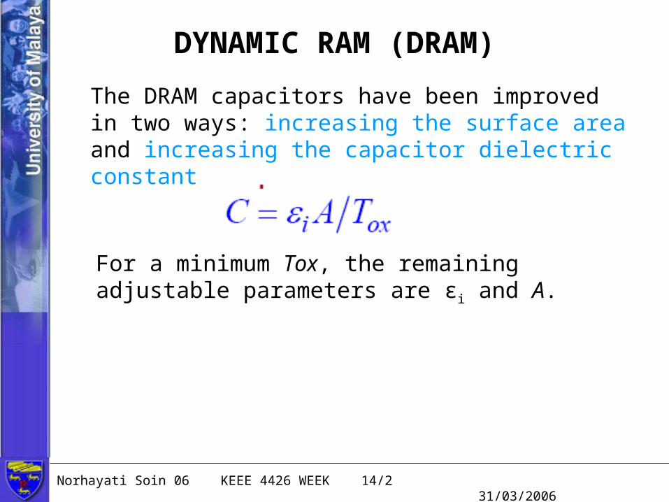
Norhayati Soin 06 KEEE 4426 WEEK 142 31032006
DYNAMIC RAM (DRAM)
For a minimum Tox the remaining adjustable parameters are εi and A
The DRAM capacitors have been improved in two ways increasing the surface area and increasing the capacitor dielectric constant
Norhayati Soin 06 KEEE 4426 WEEK 142 31032006
Trenched DRAM CellbullOne area of progress in making a capacitor with a larger surface area is to form the capacitor in a trench
bullThis technique make use of a deep trench (gt 7μm into the silicon)
bullIt has the advantage of allowing the transistors to be formed nearly planaron the surface with the trench extendingbelow the device active area
Norhayati Soin 06 KEEE 4426 WEEK 142 31032006
Trenched DRAM Cell
Fabrication results of Trenched DRAM Cell
The effect of the large surface area and the ability to thin the gate dielectric by improving the reliability of the thin oxides has resulted in a DRAM that can store more charge in smaller top surface area
Norhayati Soin 06 KEEE 4426 WEEK 142 31032006
Stacked DRAM CellAnother area of tremendous progress in DRAM technology goes in the other direction and forms the capacitors in geometries that extend above the silicon to create a large capacitor area
The large surface areas can be created using a large planar capacitor shaped like a dome or a crown
These structures also take advantage of higher-dielectric constantmaterials for the inter-level dielectric for the capacitors mdash Ta2O5 (Ba Sr)TiO3 etc
Norhayati Soin 06 KEEE 4426 WEEK 142 31032006
Stacked DRAM Cell
Norhayati Soin 06 KEEE 4426 WEEK 142 31032006
Trench Cell vs Stacked Cell
Norhayati Soin 06 KEEE 4426 WEEK 142 31032006
Trench Cell vs Stacked CellIn the trench technology the cell process is completed before the gate oxidation Therefore there is no thermal process due to cell capacitor formation after the MOSFET formation
Another advantage in the trench cell is that there is no height difference between cell array region and peripheral circuit region
In the stacked cell the height difference require high aspect ratio contact holes and difficulty in the planarization process after the cell formation
The MOSFET formation steps are followed by the stacked capacitor formation steps
Norhayati Soin 06 KEEE 4426 WEEK 142 31032006
Trench Cell vs Stacked CellThese include high temperature processing steps suchas storage node insulator (SiO2SiN) formation SiN deposition for the self-aligned contact formation etc
Salicide (Self Aligned siLICIDE) process for the source and drain of the MOSFETs should be carefully designed to endure the high temperature process steps
For applications requiring Embedded DRAM trenched cell is more attractive because the DRAM cells are formed before the MOSFETs and because there is little height difference between the cell array and other regions on the chip
Norhayati Soin 06 KEEE 4426 WEEK 142 31032006
READ ONLY MEMORY(ROM)Certain applications may require the memory to hold data that are either permanent or will not be changed frequentlyIn this case nonvolatile memory is the candidate
As the name implies Read Only Memory (ROM) has noprovision to write or update its memory contents
The programming is usually done during the manufacturingprocess or by a burning procedure prior to field use
Norhayati Soin 06 KEEE 4426 WEEK 142 31032006
READ ONLY MEMORY
Norhayati Soin 06 KEEE 4426 WEEK 142 31032006
READ ONLY MEMORY
Norhayati Soin 06 KEEE 4426 WEEK 142 31032006
READ ONLY MEMORY
Norhayati Soin 06 KEEE 4426 WEEK 142 31032006
READ ONLY MEMORY
One obvious disadvantage of the mask ROM is the fact that a new photomask must be prepared if the stored data is to be changed
This will also be accompanied by a sizable turn-aroundtime when manufacturing the new ROMs
An alternate method of implementing the ROM is with a programmable technology such as fuse or anti-fuse
In this case the ROM becomes a programmable parts hence the name PROM
One advantage of the PROM is the fact that all ROMs regardless of data content can be manufactured using the same set of photomask and fabrication procedures
Norhayati Soin 06 KEEE 4426 WEEK 142 31032006
READ ONLY MEMORY
However a one-time-only programming procedure must be applied prior to field use After the PROM is programmed its contents cannot be changed anymore
Norhayati Soin 06 KEEE 4426 WEEK 142 31032006
READ ONLY MEMORYWhy EEPROMs
Field programmable capability to wireless portable telecommunication equipment
bull1048644 True 5V or lower operationbull1048644 Compatible with CMOSBiCMOS processesbull1048644 High operation speeds and high densitybull1048644 Key to embedded systemsbull1048644 Solid-state nonvolatile memoriesbull1048644 Multi-level Encoding
Norhayati Soin 06 KEEE 4426 WEEK 142 31032006
Conventional Flash E2PROM cell Structures
bullSimilar to an ordinary MOSFET except for an extra gate buried in the silicon dioxide
bullCharges are stored in the floating gate to alter the threshold voltage of the E2PROM cell
bullSimple construction and fabrication steps
bullVery high packing density
bullFlash E2PROM and E2PROMs bullshare the same technology
Norhayati Soin 06 KEEE 4426 WEEK 142 31032006
Flash E2PROM Cell Operations
bullFor programming hot electrons are created by thelarge drain bias current
bullThese electron tunnels through the thin gate oxide and become trapped in the floating gate
Norhayati Soin 06 KEEE 4426 WEEK 142 31032006
Limitations of Existing Flash E2PROM Cells
Most cells suffer from hole trapping in the thin gateoxide during erasing
Reduction in VTH window after several cycles of erase and programming
Norhayati Soin 06 KEEE 4426 WEEK 142 31032006
Memory Circuits
Semiconductor memories are comprised of a main storage array surrounded by peripheral circuits for read and write operations
These peripheral circuits includes row and columnaddress decoders data buffersregisters sense amplifiers and charge pumps circuits
The decoders and bufferregisters are basically digital circuits and can be implemented using conventional VLSI design methodology
The sense amplifier is basically a high gain circuit that is used to differentiate the stored information with a reference voltage
Norhayati Soin 06 KEEE 4426 WEEK 142 31032006
Memory Circuits
This is especially critical if the storage element is aDRAM cell
Most memory arrays require separate high and low voltage supply to operate
In order to eliminate the need for multiple external power supplies more memory chips have built-in charge pump circuits to generate multiple voltage levels from a single supply (usually 5V or 33V)
- CHAPTER 6
- INTRODUCTION
- CLASSIFICATION OF SEMICONDUCTOR MEMORIES
- STATIC RAM (SRAM)
- Slide 5
- Slide 6
- Slide 7
- DYNAMIC RAM (DRAM)
- Slide 9
- Slide 10
- Slide 11
- Trenched DRAM Cell
- Slide 13
- Stacked DRAM Cell
- Slide 15
- Trench Cell vs Stacked Cell
- Trench Cell vs Stacked Cell
- Slide 18
- READ ONLY MEMORY(ROM)
- READ ONLY MEMORY
- Slide 21
- Slide 22
- Slide 23
- Slide 24
- Slide 25
- Conventional Flash E2PROM cell Structures
- Flash E2PROM Cell Operations
- Limitations of Existing Flash E2PROM Cells
- Memory Circuits
- Slide 30
-

Norhayati Soin 06 KEEE 4426 WEEK 142 31032006
Trenched DRAM CellbullOne area of progress in making a capacitor with a larger surface area is to form the capacitor in a trench
bullThis technique make use of a deep trench (gt 7μm into the silicon)
bullIt has the advantage of allowing the transistors to be formed nearly planaron the surface with the trench extendingbelow the device active area
Norhayati Soin 06 KEEE 4426 WEEK 142 31032006
Trenched DRAM Cell
Fabrication results of Trenched DRAM Cell
The effect of the large surface area and the ability to thin the gate dielectric by improving the reliability of the thin oxides has resulted in a DRAM that can store more charge in smaller top surface area
Norhayati Soin 06 KEEE 4426 WEEK 142 31032006
Stacked DRAM CellAnother area of tremendous progress in DRAM technology goes in the other direction and forms the capacitors in geometries that extend above the silicon to create a large capacitor area
The large surface areas can be created using a large planar capacitor shaped like a dome or a crown
These structures also take advantage of higher-dielectric constantmaterials for the inter-level dielectric for the capacitors mdash Ta2O5 (Ba Sr)TiO3 etc
Norhayati Soin 06 KEEE 4426 WEEK 142 31032006
Stacked DRAM Cell
Norhayati Soin 06 KEEE 4426 WEEK 142 31032006
Trench Cell vs Stacked Cell
Norhayati Soin 06 KEEE 4426 WEEK 142 31032006
Trench Cell vs Stacked CellIn the trench technology the cell process is completed before the gate oxidation Therefore there is no thermal process due to cell capacitor formation after the MOSFET formation
Another advantage in the trench cell is that there is no height difference between cell array region and peripheral circuit region
In the stacked cell the height difference require high aspect ratio contact holes and difficulty in the planarization process after the cell formation
The MOSFET formation steps are followed by the stacked capacitor formation steps
Norhayati Soin 06 KEEE 4426 WEEK 142 31032006
Trench Cell vs Stacked CellThese include high temperature processing steps suchas storage node insulator (SiO2SiN) formation SiN deposition for the self-aligned contact formation etc
Salicide (Self Aligned siLICIDE) process for the source and drain of the MOSFETs should be carefully designed to endure the high temperature process steps
For applications requiring Embedded DRAM trenched cell is more attractive because the DRAM cells are formed before the MOSFETs and because there is little height difference between the cell array and other regions on the chip
Norhayati Soin 06 KEEE 4426 WEEK 142 31032006
READ ONLY MEMORY(ROM)Certain applications may require the memory to hold data that are either permanent or will not be changed frequentlyIn this case nonvolatile memory is the candidate
As the name implies Read Only Memory (ROM) has noprovision to write or update its memory contents
The programming is usually done during the manufacturingprocess or by a burning procedure prior to field use
Norhayati Soin 06 KEEE 4426 WEEK 142 31032006
READ ONLY MEMORY
Norhayati Soin 06 KEEE 4426 WEEK 142 31032006
READ ONLY MEMORY
Norhayati Soin 06 KEEE 4426 WEEK 142 31032006
READ ONLY MEMORY
Norhayati Soin 06 KEEE 4426 WEEK 142 31032006
READ ONLY MEMORY
One obvious disadvantage of the mask ROM is the fact that a new photomask must be prepared if the stored data is to be changed
This will also be accompanied by a sizable turn-aroundtime when manufacturing the new ROMs
An alternate method of implementing the ROM is with a programmable technology such as fuse or anti-fuse
In this case the ROM becomes a programmable parts hence the name PROM
One advantage of the PROM is the fact that all ROMs regardless of data content can be manufactured using the same set of photomask and fabrication procedures
Norhayati Soin 06 KEEE 4426 WEEK 142 31032006
READ ONLY MEMORY
However a one-time-only programming procedure must be applied prior to field use After the PROM is programmed its contents cannot be changed anymore
Norhayati Soin 06 KEEE 4426 WEEK 142 31032006
READ ONLY MEMORYWhy EEPROMs
Field programmable capability to wireless portable telecommunication equipment
bull1048644 True 5V or lower operationbull1048644 Compatible with CMOSBiCMOS processesbull1048644 High operation speeds and high densitybull1048644 Key to embedded systemsbull1048644 Solid-state nonvolatile memoriesbull1048644 Multi-level Encoding
Norhayati Soin 06 KEEE 4426 WEEK 142 31032006
Conventional Flash E2PROM cell Structures
bullSimilar to an ordinary MOSFET except for an extra gate buried in the silicon dioxide
bullCharges are stored in the floating gate to alter the threshold voltage of the E2PROM cell
bullSimple construction and fabrication steps
bullVery high packing density
bullFlash E2PROM and E2PROMs bullshare the same technology
Norhayati Soin 06 KEEE 4426 WEEK 142 31032006
Flash E2PROM Cell Operations
bullFor programming hot electrons are created by thelarge drain bias current
bullThese electron tunnels through the thin gate oxide and become trapped in the floating gate
Norhayati Soin 06 KEEE 4426 WEEK 142 31032006
Limitations of Existing Flash E2PROM Cells
Most cells suffer from hole trapping in the thin gateoxide during erasing
Reduction in VTH window after several cycles of erase and programming
Norhayati Soin 06 KEEE 4426 WEEK 142 31032006
Memory Circuits
Semiconductor memories are comprised of a main storage array surrounded by peripheral circuits for read and write operations
These peripheral circuits includes row and columnaddress decoders data buffersregisters sense amplifiers and charge pumps circuits
The decoders and bufferregisters are basically digital circuits and can be implemented using conventional VLSI design methodology
The sense amplifier is basically a high gain circuit that is used to differentiate the stored information with a reference voltage
Norhayati Soin 06 KEEE 4426 WEEK 142 31032006
Memory Circuits
This is especially critical if the storage element is aDRAM cell
Most memory arrays require separate high and low voltage supply to operate
In order to eliminate the need for multiple external power supplies more memory chips have built-in charge pump circuits to generate multiple voltage levels from a single supply (usually 5V or 33V)
- CHAPTER 6
- INTRODUCTION
- CLASSIFICATION OF SEMICONDUCTOR MEMORIES
- STATIC RAM (SRAM)
- Slide 5
- Slide 6
- Slide 7
- DYNAMIC RAM (DRAM)
- Slide 9
- Slide 10
- Slide 11
- Trenched DRAM Cell
- Slide 13
- Stacked DRAM Cell
- Slide 15
- Trench Cell vs Stacked Cell
- Trench Cell vs Stacked Cell
- Slide 18
- READ ONLY MEMORY(ROM)
- READ ONLY MEMORY
- Slide 21
- Slide 22
- Slide 23
- Slide 24
- Slide 25
- Conventional Flash E2PROM cell Structures
- Flash E2PROM Cell Operations
- Limitations of Existing Flash E2PROM Cells
- Memory Circuits
- Slide 30
-
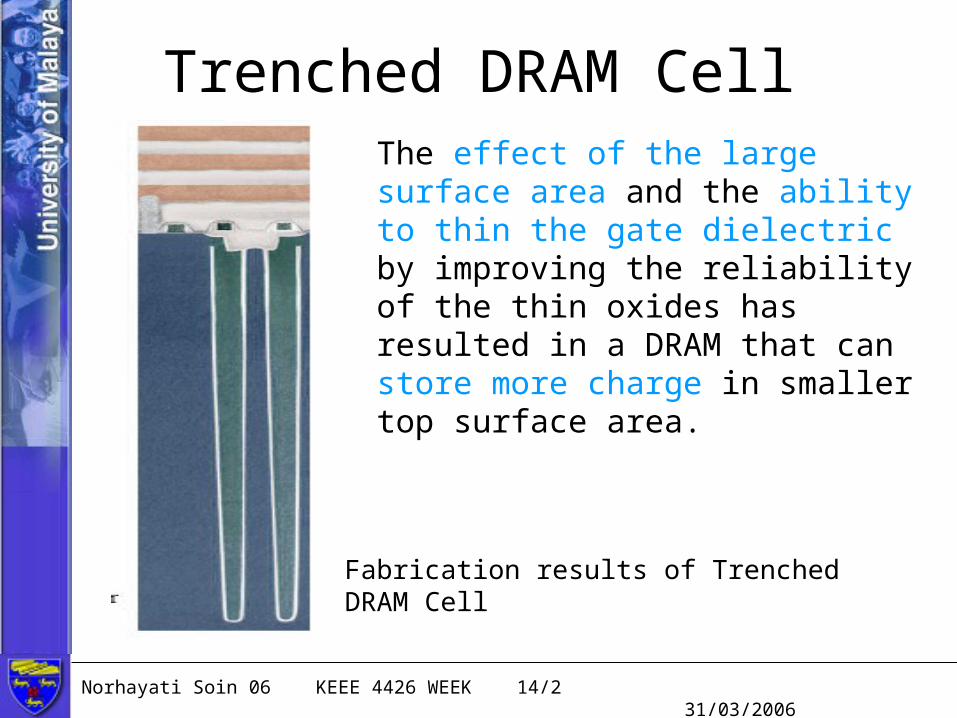
Norhayati Soin 06 KEEE 4426 WEEK 142 31032006
Stacked DRAM Cell
Norhayati Soin 06 KEEE 4426 WEEK 142 31032006
Trench Cell vs Stacked Cell
Norhayati Soin 06 KEEE 4426 WEEK 142 31032006
Trench Cell vs Stacked CellIn the trench technology the cell process is completed before the gate oxidation Therefore there is no thermal process due to cell capacitor formation after the MOSFET formation
Another advantage in the trench cell is that there is no height difference between cell array region and peripheral circuit region
In the stacked cell the height difference require high aspect ratio contact holes and difficulty in the planarization process after the cell formation
The MOSFET formation steps are followed by the stacked capacitor formation steps
Norhayati Soin 06 KEEE 4426 WEEK 142 31032006
Trench Cell vs Stacked CellThese include high temperature processing steps suchas storage node insulator (SiO2SiN) formation SiN deposition for the self-aligned contact formation etc
Salicide (Self Aligned siLICIDE) process for the source and drain of the MOSFETs should be carefully designed to endure the high temperature process steps
For applications requiring Embedded DRAM trenched cell is more attractive because the DRAM cells are formed before the MOSFETs and because there is little height difference between the cell array and other regions on the chip
Norhayati Soin 06 KEEE 4426 WEEK 142 31032006
READ ONLY MEMORY(ROM)Certain applications may require the memory to hold data that are either permanent or will not be changed frequentlyIn this case nonvolatile memory is the candidate
As the name implies Read Only Memory (ROM) has noprovision to write or update its memory contents
The programming is usually done during the manufacturingprocess or by a burning procedure prior to field use
Norhayati Soin 06 KEEE 4426 WEEK 142 31032006
READ ONLY MEMORY
Norhayati Soin 06 KEEE 4426 WEEK 142 31032006
READ ONLY MEMORY
Norhayati Soin 06 KEEE 4426 WEEK 142 31032006
READ ONLY MEMORY
Norhayati Soin 06 KEEE 4426 WEEK 142 31032006
READ ONLY MEMORY
One obvious disadvantage of the mask ROM is the fact that a new photomask must be prepared if the stored data is to be changed
This will also be accompanied by a sizable turn-aroundtime when manufacturing the new ROMs
An alternate method of implementing the ROM is with a programmable technology such as fuse or anti-fuse
In this case the ROM becomes a programmable parts hence the name PROM
One advantage of the PROM is the fact that all ROMs regardless of data content can be manufactured using the same set of photomask and fabrication procedures
Norhayati Soin 06 KEEE 4426 WEEK 142 31032006
READ ONLY MEMORY
However a one-time-only programming procedure must be applied prior to field use After the PROM is programmed its contents cannot be changed anymore
Norhayati Soin 06 KEEE 4426 WEEK 142 31032006
READ ONLY MEMORYWhy EEPROMs
Field programmable capability to wireless portable telecommunication equipment
bull1048644 True 5V or lower operationbull1048644 Compatible with CMOSBiCMOS processesbull1048644 High operation speeds and high densitybull1048644 Key to embedded systemsbull1048644 Solid-state nonvolatile memoriesbull1048644 Multi-level Encoding
Norhayati Soin 06 KEEE 4426 WEEK 142 31032006
Conventional Flash E2PROM cell Structures
bullSimilar to an ordinary MOSFET except for an extra gate buried in the silicon dioxide
bullCharges are stored in the floating gate to alter the threshold voltage of the E2PROM cell
bullSimple construction and fabrication steps
bullVery high packing density
bullFlash E2PROM and E2PROMs bullshare the same technology
Norhayati Soin 06 KEEE 4426 WEEK 142 31032006
Flash E2PROM Cell Operations
bullFor programming hot electrons are created by thelarge drain bias current
bullThese electron tunnels through the thin gate oxide and become trapped in the floating gate
Norhayati Soin 06 KEEE 4426 WEEK 142 31032006
Limitations of Existing Flash E2PROM Cells
Most cells suffer from hole trapping in the thin gateoxide during erasing
Reduction in VTH window after several cycles of erase and programming
Norhayati Soin 06 KEEE 4426 WEEK 142 31032006
Memory Circuits
Semiconductor memories are comprised of a main storage array surrounded by peripheral circuits for read and write operations
These peripheral circuits includes row and columnaddress decoders data buffersregisters sense amplifiers and charge pumps circuits
The decoders and bufferregisters are basically digital circuits and can be implemented using conventional VLSI design methodology
The sense amplifier is basically a high gain circuit that is used to differentiate the stored information with a reference voltage
Norhayati Soin 06 KEEE 4426 WEEK 142 31032006
Memory Circuits
This is especially critical if the storage element is aDRAM cell
Most memory arrays require separate high and low voltage supply to operate
In order to eliminate the need for multiple external power supplies more memory chips have built-in charge pump circuits to generate multiple voltage levels from a single supply (usually 5V or 33V)
- CHAPTER 6
- INTRODUCTION
- CLASSIFICATION OF SEMICONDUCTOR MEMORIES
- STATIC RAM (SRAM)
- Slide 5
- Slide 6
- Slide 7
- DYNAMIC RAM (DRAM)
- Slide 9
- Slide 10
- Slide 11
- Trenched DRAM Cell
- Slide 13
- Stacked DRAM Cell
- Slide 15
- Trench Cell vs Stacked Cell
- Trench Cell vs Stacked Cell
- Slide 18
- READ ONLY MEMORY(ROM)
- READ ONLY MEMORY
- Slide 21
- Slide 22
- Slide 23
- Slide 24
- Slide 25
- Conventional Flash E2PROM cell Structures
- Flash E2PROM Cell Operations
- Limitations of Existing Flash E2PROM Cells
- Memory Circuits
- Slide 30
-
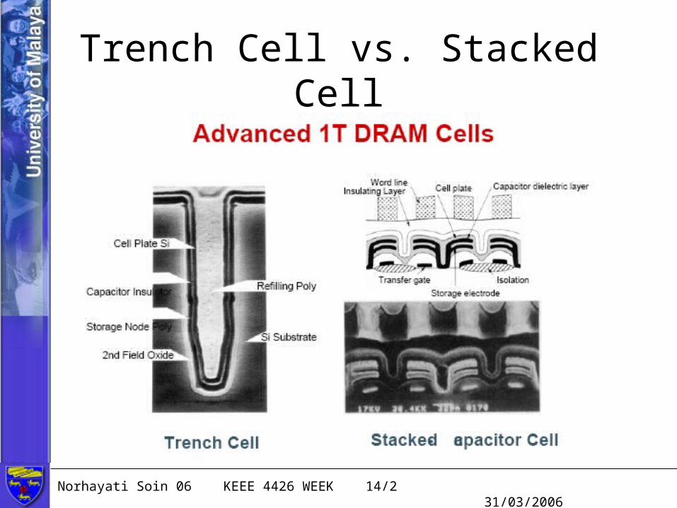
Norhayati Soin 06 KEEE 4426 WEEK 142 31032006
Trench Cell vs Stacked CellThese include high temperature processing steps suchas storage node insulator (SiO2SiN) formation SiN deposition for the self-aligned contact formation etc
Salicide (Self Aligned siLICIDE) process for the source and drain of the MOSFETs should be carefully designed to endure the high temperature process steps
For applications requiring Embedded DRAM trenched cell is more attractive because the DRAM cells are formed before the MOSFETs and because there is little height difference between the cell array and other regions on the chip
Norhayati Soin 06 KEEE 4426 WEEK 142 31032006
READ ONLY MEMORY(ROM)Certain applications may require the memory to hold data that are either permanent or will not be changed frequentlyIn this case nonvolatile memory is the candidate
As the name implies Read Only Memory (ROM) has noprovision to write or update its memory contents
The programming is usually done during the manufacturingprocess or by a burning procedure prior to field use
Norhayati Soin 06 KEEE 4426 WEEK 142 31032006
READ ONLY MEMORY
Norhayati Soin 06 KEEE 4426 WEEK 142 31032006
READ ONLY MEMORY
Norhayati Soin 06 KEEE 4426 WEEK 142 31032006
READ ONLY MEMORY
Norhayati Soin 06 KEEE 4426 WEEK 142 31032006
READ ONLY MEMORY
One obvious disadvantage of the mask ROM is the fact that a new photomask must be prepared if the stored data is to be changed
This will also be accompanied by a sizable turn-aroundtime when manufacturing the new ROMs
An alternate method of implementing the ROM is with a programmable technology such as fuse or anti-fuse
In this case the ROM becomes a programmable parts hence the name PROM
One advantage of the PROM is the fact that all ROMs regardless of data content can be manufactured using the same set of photomask and fabrication procedures
Norhayati Soin 06 KEEE 4426 WEEK 142 31032006
READ ONLY MEMORY
However a one-time-only programming procedure must be applied prior to field use After the PROM is programmed its contents cannot be changed anymore
Norhayati Soin 06 KEEE 4426 WEEK 142 31032006
READ ONLY MEMORYWhy EEPROMs
Field programmable capability to wireless portable telecommunication equipment
bull1048644 True 5V or lower operationbull1048644 Compatible with CMOSBiCMOS processesbull1048644 High operation speeds and high densitybull1048644 Key to embedded systemsbull1048644 Solid-state nonvolatile memoriesbull1048644 Multi-level Encoding
Norhayati Soin 06 KEEE 4426 WEEK 142 31032006
Conventional Flash E2PROM cell Structures
bullSimilar to an ordinary MOSFET except for an extra gate buried in the silicon dioxide
bullCharges are stored in the floating gate to alter the threshold voltage of the E2PROM cell
bullSimple construction and fabrication steps
bullVery high packing density
bullFlash E2PROM and E2PROMs bullshare the same technology
Norhayati Soin 06 KEEE 4426 WEEK 142 31032006
Flash E2PROM Cell Operations
bullFor programming hot electrons are created by thelarge drain bias current
bullThese electron tunnels through the thin gate oxide and become trapped in the floating gate
Norhayati Soin 06 KEEE 4426 WEEK 142 31032006
Limitations of Existing Flash E2PROM Cells
Most cells suffer from hole trapping in the thin gateoxide during erasing
Reduction in VTH window after several cycles of erase and programming
Norhayati Soin 06 KEEE 4426 WEEK 142 31032006
Memory Circuits
Semiconductor memories are comprised of a main storage array surrounded by peripheral circuits for read and write operations
These peripheral circuits includes row and columnaddress decoders data buffersregisters sense amplifiers and charge pumps circuits
The decoders and bufferregisters are basically digital circuits and can be implemented using conventional VLSI design methodology
The sense amplifier is basically a high gain circuit that is used to differentiate the stored information with a reference voltage
Norhayati Soin 06 KEEE 4426 WEEK 142 31032006
Memory Circuits
This is especially critical if the storage element is aDRAM cell
Most memory arrays require separate high and low voltage supply to operate
In order to eliminate the need for multiple external power supplies more memory chips have built-in charge pump circuits to generate multiple voltage levels from a single supply (usually 5V or 33V)
- CHAPTER 6
- INTRODUCTION
- CLASSIFICATION OF SEMICONDUCTOR MEMORIES
- STATIC RAM (SRAM)
- Slide 5
- Slide 6
- Slide 7
- DYNAMIC RAM (DRAM)
- Slide 9
- Slide 10
- Slide 11
- Trenched DRAM Cell
- Slide 13
- Stacked DRAM Cell
- Slide 15
- Trench Cell vs Stacked Cell
- Trench Cell vs Stacked Cell
- Slide 18
- READ ONLY MEMORY(ROM)
- READ ONLY MEMORY
- Slide 21
- Slide 22
- Slide 23
- Slide 24
- Slide 25
- Conventional Flash E2PROM cell Structures
- Flash E2PROM Cell Operations
- Limitations of Existing Flash E2PROM Cells
- Memory Circuits
- Slide 30
-
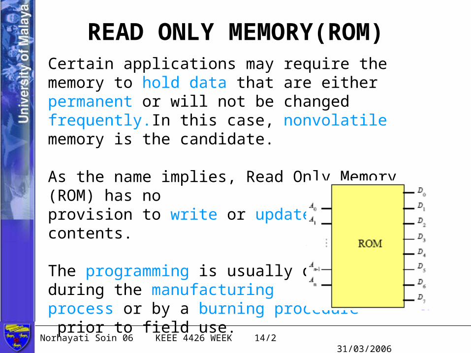
Norhayati Soin 06 KEEE 4426 WEEK 142 31032006
READ ONLY MEMORY
Norhayati Soin 06 KEEE 4426 WEEK 142 31032006
READ ONLY MEMORY
Norhayati Soin 06 KEEE 4426 WEEK 142 31032006
READ ONLY MEMORY
Norhayati Soin 06 KEEE 4426 WEEK 142 31032006
READ ONLY MEMORY
One obvious disadvantage of the mask ROM is the fact that a new photomask must be prepared if the stored data is to be changed
This will also be accompanied by a sizable turn-aroundtime when manufacturing the new ROMs
An alternate method of implementing the ROM is with a programmable technology such as fuse or anti-fuse
In this case the ROM becomes a programmable parts hence the name PROM
One advantage of the PROM is the fact that all ROMs regardless of data content can be manufactured using the same set of photomask and fabrication procedures
Norhayati Soin 06 KEEE 4426 WEEK 142 31032006
READ ONLY MEMORY
However a one-time-only programming procedure must be applied prior to field use After the PROM is programmed its contents cannot be changed anymore
Norhayati Soin 06 KEEE 4426 WEEK 142 31032006
READ ONLY MEMORYWhy EEPROMs
Field programmable capability to wireless portable telecommunication equipment
bull1048644 True 5V or lower operationbull1048644 Compatible with CMOSBiCMOS processesbull1048644 High operation speeds and high densitybull1048644 Key to embedded systemsbull1048644 Solid-state nonvolatile memoriesbull1048644 Multi-level Encoding
Norhayati Soin 06 KEEE 4426 WEEK 142 31032006
Conventional Flash E2PROM cell Structures
bullSimilar to an ordinary MOSFET except for an extra gate buried in the silicon dioxide
bullCharges are stored in the floating gate to alter the threshold voltage of the E2PROM cell
bullSimple construction and fabrication steps
bullVery high packing density
bullFlash E2PROM and E2PROMs bullshare the same technology
Norhayati Soin 06 KEEE 4426 WEEK 142 31032006
Flash E2PROM Cell Operations
bullFor programming hot electrons are created by thelarge drain bias current
bullThese electron tunnels through the thin gate oxide and become trapped in the floating gate
Norhayati Soin 06 KEEE 4426 WEEK 142 31032006
Limitations of Existing Flash E2PROM Cells
Most cells suffer from hole trapping in the thin gateoxide during erasing
Reduction in VTH window after several cycles of erase and programming
Norhayati Soin 06 KEEE 4426 WEEK 142 31032006
Memory Circuits
Semiconductor memories are comprised of a main storage array surrounded by peripheral circuits for read and write operations
These peripheral circuits includes row and columnaddress decoders data buffersregisters sense amplifiers and charge pumps circuits
The decoders and bufferregisters are basically digital circuits and can be implemented using conventional VLSI design methodology
The sense amplifier is basically a high gain circuit that is used to differentiate the stored information with a reference voltage
Norhayati Soin 06 KEEE 4426 WEEK 142 31032006
Memory Circuits
This is especially critical if the storage element is aDRAM cell
Most memory arrays require separate high and low voltage supply to operate
In order to eliminate the need for multiple external power supplies more memory chips have built-in charge pump circuits to generate multiple voltage levels from a single supply (usually 5V or 33V)
- CHAPTER 6
- INTRODUCTION
- CLASSIFICATION OF SEMICONDUCTOR MEMORIES
- STATIC RAM (SRAM)
- Slide 5
- Slide 6
- Slide 7
- DYNAMIC RAM (DRAM)
- Slide 9
- Slide 10
- Slide 11
- Trenched DRAM Cell
- Slide 13
- Stacked DRAM Cell
- Slide 15
- Trench Cell vs Stacked Cell
- Trench Cell vs Stacked Cell
- Slide 18
- READ ONLY MEMORY(ROM)
- READ ONLY MEMORY
- Slide 21
- Slide 22
- Slide 23
- Slide 24
- Slide 25
- Conventional Flash E2PROM cell Structures
- Flash E2PROM Cell Operations
- Limitations of Existing Flash E2PROM Cells
- Memory Circuits
- Slide 30
-
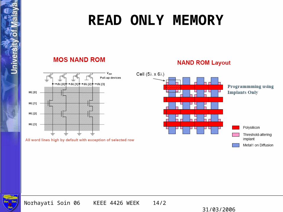
Norhayati Soin 06 KEEE 4426 WEEK 142 31032006
READ ONLY MEMORY
Norhayati Soin 06 KEEE 4426 WEEK 142 31032006
READ ONLY MEMORY
Norhayati Soin 06 KEEE 4426 WEEK 142 31032006
READ ONLY MEMORY
One obvious disadvantage of the mask ROM is the fact that a new photomask must be prepared if the stored data is to be changed
This will also be accompanied by a sizable turn-aroundtime when manufacturing the new ROMs
An alternate method of implementing the ROM is with a programmable technology such as fuse or anti-fuse
In this case the ROM becomes a programmable parts hence the name PROM
One advantage of the PROM is the fact that all ROMs regardless of data content can be manufactured using the same set of photomask and fabrication procedures
Norhayati Soin 06 KEEE 4426 WEEK 142 31032006
READ ONLY MEMORY
However a one-time-only programming procedure must be applied prior to field use After the PROM is programmed its contents cannot be changed anymore
Norhayati Soin 06 KEEE 4426 WEEK 142 31032006
READ ONLY MEMORYWhy EEPROMs
Field programmable capability to wireless portable telecommunication equipment
bull1048644 True 5V or lower operationbull1048644 Compatible with CMOSBiCMOS processesbull1048644 High operation speeds and high densitybull1048644 Key to embedded systemsbull1048644 Solid-state nonvolatile memoriesbull1048644 Multi-level Encoding
Norhayati Soin 06 KEEE 4426 WEEK 142 31032006
Conventional Flash E2PROM cell Structures
bullSimilar to an ordinary MOSFET except for an extra gate buried in the silicon dioxide
bullCharges are stored in the floating gate to alter the threshold voltage of the E2PROM cell
bullSimple construction and fabrication steps
bullVery high packing density
bullFlash E2PROM and E2PROMs bullshare the same technology
Norhayati Soin 06 KEEE 4426 WEEK 142 31032006
Flash E2PROM Cell Operations
bullFor programming hot electrons are created by thelarge drain bias current
bullThese electron tunnels through the thin gate oxide and become trapped in the floating gate
Norhayati Soin 06 KEEE 4426 WEEK 142 31032006
Limitations of Existing Flash E2PROM Cells
Most cells suffer from hole trapping in the thin gateoxide during erasing
Reduction in VTH window after several cycles of erase and programming
Norhayati Soin 06 KEEE 4426 WEEK 142 31032006
Memory Circuits
Semiconductor memories are comprised of a main storage array surrounded by peripheral circuits for read and write operations
These peripheral circuits includes row and columnaddress decoders data buffersregisters sense amplifiers and charge pumps circuits
The decoders and bufferregisters are basically digital circuits and can be implemented using conventional VLSI design methodology
The sense amplifier is basically a high gain circuit that is used to differentiate the stored information with a reference voltage
Norhayati Soin 06 KEEE 4426 WEEK 142 31032006
Memory Circuits
This is especially critical if the storage element is aDRAM cell
Most memory arrays require separate high and low voltage supply to operate
In order to eliminate the need for multiple external power supplies more memory chips have built-in charge pump circuits to generate multiple voltage levels from a single supply (usually 5V or 33V)
- CHAPTER 6
- INTRODUCTION
- CLASSIFICATION OF SEMICONDUCTOR MEMORIES
- STATIC RAM (SRAM)
- Slide 5
- Slide 6
- Slide 7
- DYNAMIC RAM (DRAM)
- Slide 9
- Slide 10
- Slide 11
- Trenched DRAM Cell
- Slide 13
- Stacked DRAM Cell
- Slide 15
- Trench Cell vs Stacked Cell
- Trench Cell vs Stacked Cell
- Slide 18
- READ ONLY MEMORY(ROM)
- READ ONLY MEMORY
- Slide 21
- Slide 22
- Slide 23
- Slide 24
- Slide 25
- Conventional Flash E2PROM cell Structures
- Flash E2PROM Cell Operations
- Limitations of Existing Flash E2PROM Cells
- Memory Circuits
- Slide 30
-
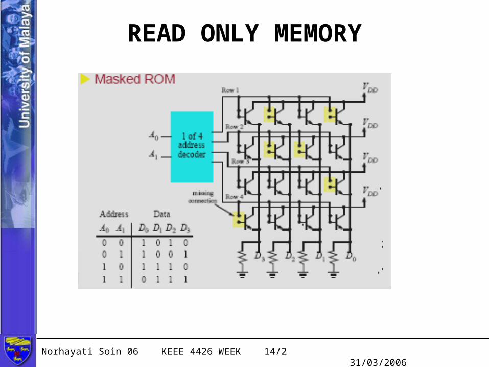
Norhayati Soin 06 KEEE 4426 WEEK 142 31032006
READ ONLY MEMORY
Norhayati Soin 06 KEEE 4426 WEEK 142 31032006
READ ONLY MEMORY
One obvious disadvantage of the mask ROM is the fact that a new photomask must be prepared if the stored data is to be changed
This will also be accompanied by a sizable turn-aroundtime when manufacturing the new ROMs
An alternate method of implementing the ROM is with a programmable technology such as fuse or anti-fuse
In this case the ROM becomes a programmable parts hence the name PROM
One advantage of the PROM is the fact that all ROMs regardless of data content can be manufactured using the same set of photomask and fabrication procedures
Norhayati Soin 06 KEEE 4426 WEEK 142 31032006
READ ONLY MEMORY
However a one-time-only programming procedure must be applied prior to field use After the PROM is programmed its contents cannot be changed anymore
Norhayati Soin 06 KEEE 4426 WEEK 142 31032006
READ ONLY MEMORYWhy EEPROMs
Field programmable capability to wireless portable telecommunication equipment
bull1048644 True 5V or lower operationbull1048644 Compatible with CMOSBiCMOS processesbull1048644 High operation speeds and high densitybull1048644 Key to embedded systemsbull1048644 Solid-state nonvolatile memoriesbull1048644 Multi-level Encoding
Norhayati Soin 06 KEEE 4426 WEEK 142 31032006
Conventional Flash E2PROM cell Structures
bullSimilar to an ordinary MOSFET except for an extra gate buried in the silicon dioxide
bullCharges are stored in the floating gate to alter the threshold voltage of the E2PROM cell
bullSimple construction and fabrication steps
bullVery high packing density
bullFlash E2PROM and E2PROMs bullshare the same technology
Norhayati Soin 06 KEEE 4426 WEEK 142 31032006
Flash E2PROM Cell Operations
bullFor programming hot electrons are created by thelarge drain bias current
bullThese electron tunnels through the thin gate oxide and become trapped in the floating gate
Norhayati Soin 06 KEEE 4426 WEEK 142 31032006
Limitations of Existing Flash E2PROM Cells
Most cells suffer from hole trapping in the thin gateoxide during erasing
Reduction in VTH window after several cycles of erase and programming
Norhayati Soin 06 KEEE 4426 WEEK 142 31032006
Memory Circuits
Semiconductor memories are comprised of a main storage array surrounded by peripheral circuits for read and write operations
These peripheral circuits includes row and columnaddress decoders data buffersregisters sense amplifiers and charge pumps circuits
The decoders and bufferregisters are basically digital circuits and can be implemented using conventional VLSI design methodology
The sense amplifier is basically a high gain circuit that is used to differentiate the stored information with a reference voltage
Norhayati Soin 06 KEEE 4426 WEEK 142 31032006
Memory Circuits
This is especially critical if the storage element is aDRAM cell
Most memory arrays require separate high and low voltage supply to operate
In order to eliminate the need for multiple external power supplies more memory chips have built-in charge pump circuits to generate multiple voltage levels from a single supply (usually 5V or 33V)
- CHAPTER 6
- INTRODUCTION
- CLASSIFICATION OF SEMICONDUCTOR MEMORIES
- STATIC RAM (SRAM)
- Slide 5
- Slide 6
- Slide 7
- DYNAMIC RAM (DRAM)
- Slide 9
- Slide 10
- Slide 11
- Trenched DRAM Cell
- Slide 13
- Stacked DRAM Cell
- Slide 15
- Trench Cell vs Stacked Cell
- Trench Cell vs Stacked Cell
- Slide 18
- READ ONLY MEMORY(ROM)
- READ ONLY MEMORY
- Slide 21
- Slide 22
- Slide 23
- Slide 24
- Slide 25
- Conventional Flash E2PROM cell Structures
- Flash E2PROM Cell Operations
- Limitations of Existing Flash E2PROM Cells
- Memory Circuits
- Slide 30
-

Norhayati Soin 06 KEEE 4426 WEEK 142 31032006
READ ONLY MEMORY
However a one-time-only programming procedure must be applied prior to field use After the PROM is programmed its contents cannot be changed anymore
Norhayati Soin 06 KEEE 4426 WEEK 142 31032006
READ ONLY MEMORYWhy EEPROMs
Field programmable capability to wireless portable telecommunication equipment
bull1048644 True 5V or lower operationbull1048644 Compatible with CMOSBiCMOS processesbull1048644 High operation speeds and high densitybull1048644 Key to embedded systemsbull1048644 Solid-state nonvolatile memoriesbull1048644 Multi-level Encoding
Norhayati Soin 06 KEEE 4426 WEEK 142 31032006
Conventional Flash E2PROM cell Structures
bullSimilar to an ordinary MOSFET except for an extra gate buried in the silicon dioxide
bullCharges are stored in the floating gate to alter the threshold voltage of the E2PROM cell
bullSimple construction and fabrication steps
bullVery high packing density
bullFlash E2PROM and E2PROMs bullshare the same technology
Norhayati Soin 06 KEEE 4426 WEEK 142 31032006
Flash E2PROM Cell Operations
bullFor programming hot electrons are created by thelarge drain bias current
bullThese electron tunnels through the thin gate oxide and become trapped in the floating gate
Norhayati Soin 06 KEEE 4426 WEEK 142 31032006
Limitations of Existing Flash E2PROM Cells
Most cells suffer from hole trapping in the thin gateoxide during erasing
Reduction in VTH window after several cycles of erase and programming
Norhayati Soin 06 KEEE 4426 WEEK 142 31032006
Memory Circuits
Semiconductor memories are comprised of a main storage array surrounded by peripheral circuits for read and write operations
These peripheral circuits includes row and columnaddress decoders data buffersregisters sense amplifiers and charge pumps circuits
The decoders and bufferregisters are basically digital circuits and can be implemented using conventional VLSI design methodology
The sense amplifier is basically a high gain circuit that is used to differentiate the stored information with a reference voltage
Norhayati Soin 06 KEEE 4426 WEEK 142 31032006
Memory Circuits
This is especially critical if the storage element is aDRAM cell
Most memory arrays require separate high and low voltage supply to operate
In order to eliminate the need for multiple external power supplies more memory chips have built-in charge pump circuits to generate multiple voltage levels from a single supply (usually 5V or 33V)
- CHAPTER 6
- INTRODUCTION
- CLASSIFICATION OF SEMICONDUCTOR MEMORIES
- STATIC RAM (SRAM)
- Slide 5
- Slide 6
- Slide 7
- DYNAMIC RAM (DRAM)
- Slide 9
- Slide 10
- Slide 11
- Trenched DRAM Cell
- Slide 13
- Stacked DRAM Cell
- Slide 15
- Trench Cell vs Stacked Cell
- Trench Cell vs Stacked Cell
- Slide 18
- READ ONLY MEMORY(ROM)
- READ ONLY MEMORY
- Slide 21
- Slide 22
- Slide 23
- Slide 24
- Slide 25
- Conventional Flash E2PROM cell Structures
- Flash E2PROM Cell Operations
- Limitations of Existing Flash E2PROM Cells
- Memory Circuits
- Slide 30
-
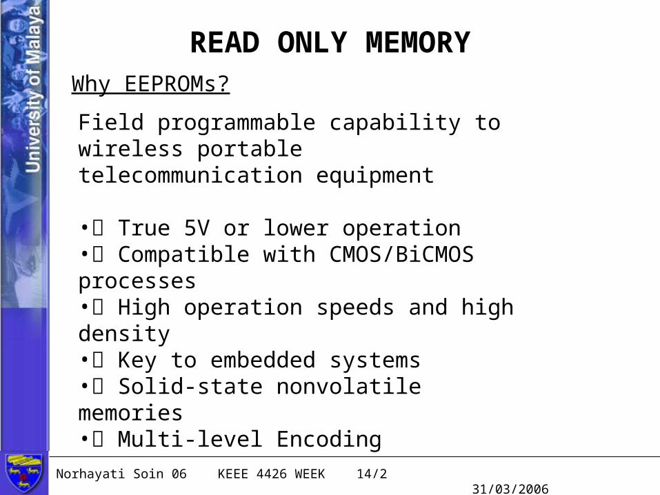
Norhayati Soin 06 KEEE 4426 WEEK 142 31032006
Limitations of Existing Flash E2PROM Cells
Most cells suffer from hole trapping in the thin gateoxide during erasing
Reduction in VTH window after several cycles of erase and programming
Norhayati Soin 06 KEEE 4426 WEEK 142 31032006
Memory Circuits
Semiconductor memories are comprised of a main storage array surrounded by peripheral circuits for read and write operations
These peripheral circuits includes row and columnaddress decoders data buffersregisters sense amplifiers and charge pumps circuits
The decoders and bufferregisters are basically digital circuits and can be implemented using conventional VLSI design methodology
The sense amplifier is basically a high gain circuit that is used to differentiate the stored information with a reference voltage
Norhayati Soin 06 KEEE 4426 WEEK 142 31032006
Memory Circuits
This is especially critical if the storage element is aDRAM cell
Most memory arrays require separate high and low voltage supply to operate
In order to eliminate the need for multiple external power supplies more memory chips have built-in charge pump circuits to generate multiple voltage levels from a single supply (usually 5V or 33V)
- CHAPTER 6
- INTRODUCTION
- CLASSIFICATION OF SEMICONDUCTOR MEMORIES
- STATIC RAM (SRAM)
- Slide 5
- Slide 6
- Slide 7
- DYNAMIC RAM (DRAM)
- Slide 9
- Slide 10
- Slide 11
- Trenched DRAM Cell
- Slide 13
- Stacked DRAM Cell
- Slide 15
- Trench Cell vs Stacked Cell
- Trench Cell vs Stacked Cell
- Slide 18
- READ ONLY MEMORY(ROM)
- READ ONLY MEMORY
- Slide 21
- Slide 22
- Slide 23
- Slide 24
- Slide 25
- Conventional Flash E2PROM cell Structures
- Flash E2PROM Cell Operations
- Limitations of Existing Flash E2PROM Cells
- Memory Circuits
- Slide 30
-
Norhayati Soin 06 KEEE 4426 WEEK 142 31032006
Memory Circuits
Semiconductor memories are comprised of a main storage array surrounded by peripheral circuits for read and write operations
These peripheral circuits includes row and columnaddress decoders data buffersregisters sense amplifiers and charge pumps circuits
The decoders and bufferregisters are basically digital circuits and can be implemented using conventional VLSI design methodology
The sense amplifier is basically a high gain circuit that is used to differentiate the stored information with a reference voltage
Norhayati Soin 06 KEEE 4426 WEEK 142 31032006
Memory Circuits
This is especially critical if the storage element is aDRAM cell
Most memory arrays require separate high and low voltage supply to operate
In order to eliminate the need for multiple external power supplies more memory chips have built-in charge pump circuits to generate multiple voltage levels from a single supply (usually 5V or 33V)
- CHAPTER 6
- INTRODUCTION
- CLASSIFICATION OF SEMICONDUCTOR MEMORIES
- STATIC RAM (SRAM)
- Slide 5
- Slide 6
- Slide 7
- DYNAMIC RAM (DRAM)
- Slide 9
- Slide 10
- Slide 11
- Trenched DRAM Cell
- Slide 13
- Stacked DRAM Cell
- Slide 15
- Trench Cell vs Stacked Cell
- Trench Cell vs Stacked Cell
- Slide 18
- READ ONLY MEMORY(ROM)
- READ ONLY MEMORY
- Slide 21
- Slide 22
- Slide 23
- Slide 24
- Slide 25
- Conventional Flash E2PROM cell Structures
- Flash E2PROM Cell Operations
- Limitations of Existing Flash E2PROM Cells
- Memory Circuits
- Slide 30
-