novel devices circuits computing - ece.ucsb.edustrukov/ece594bbwinter2013/veiwgraphs/cmol.… ·...
TRANSCRIPT
Novel Devices and Circuits for Computing
UCSB 594BBWinter 2013
Lecture 7: CMOL
OutlineOutline
• CMOLCMOL– Main idea
3D CMOL– 3D CMOL
• CMOL memory
• CMOL logic– General purporse
– Threshold logic
– Pattern matching

CMOS/Nano Hybrids: The IdeaHybrid CMOS/Memristor Circuits
historic (first?) version: current version:
add‐on
topnanowire level
add o
CMOSk
bottom nanowire
similar two‐terminalnanodevices
at each crosspoint J. Heath et al. Science 280 1716 (1998)
stack
level
WHAT: • CMOS stack + simple nano add‐on• nanowire crossbar + two‐terminal devices (latching switches)
WHY: • CMOS functionality and infrastructure intact • inexpensive fabrication of reproducible nanodevices• advanced lithography with no need in layer alignment
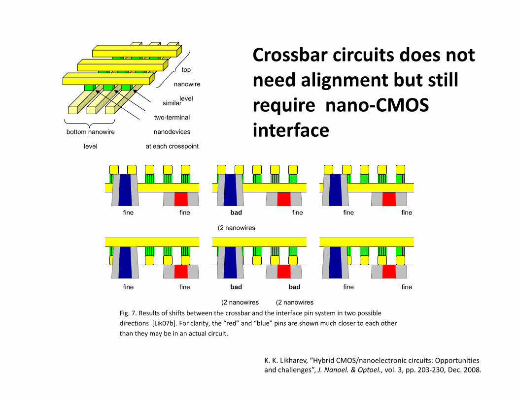
Crossbar circuits does not d li b ill
top
need alignment but still require nano‐CMOS i t f
nanowire
levelsimilar
two-terminal
interfacebottom nanowire
level
nanodevices
at each crosspoint
fine fine bad fine fine fine
(2 i (2 nanowires
fine fine bad bad fine fine
(2 nanowires (2 nanowires Fig. 7. Results of shifts between the crossbar and the interface pin system in two possible directions [Lik07b]. For clarity, the “red” and “blue” pins are shown much closer to each other [ ] y, pthan they may be in an actual circuit.
K. K. Likharev, “Hybrid CMOS/nanoelectronic circuits: Opportunities and challenges”, J. Nanoel. & Optoel., vol. 3, pp. 203‐230, Dec. 2008.
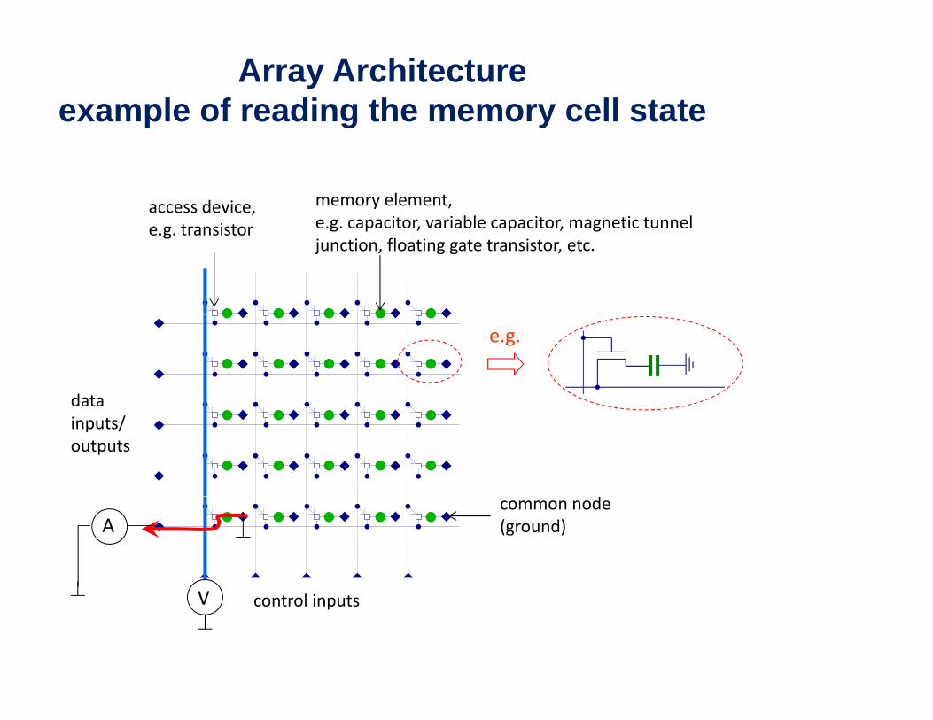
Array Architectureexample of reading the memory cell state
access device, i
memory element,e g capacitor variable capacitor magnetic tunnele.g. transistor e.g. capacitor, variable capacitor, magnetic tunnel junction, floating gate transistor, etc.
data
e.g.
datainputs/outputs
Acommon node (ground)
control inputsV
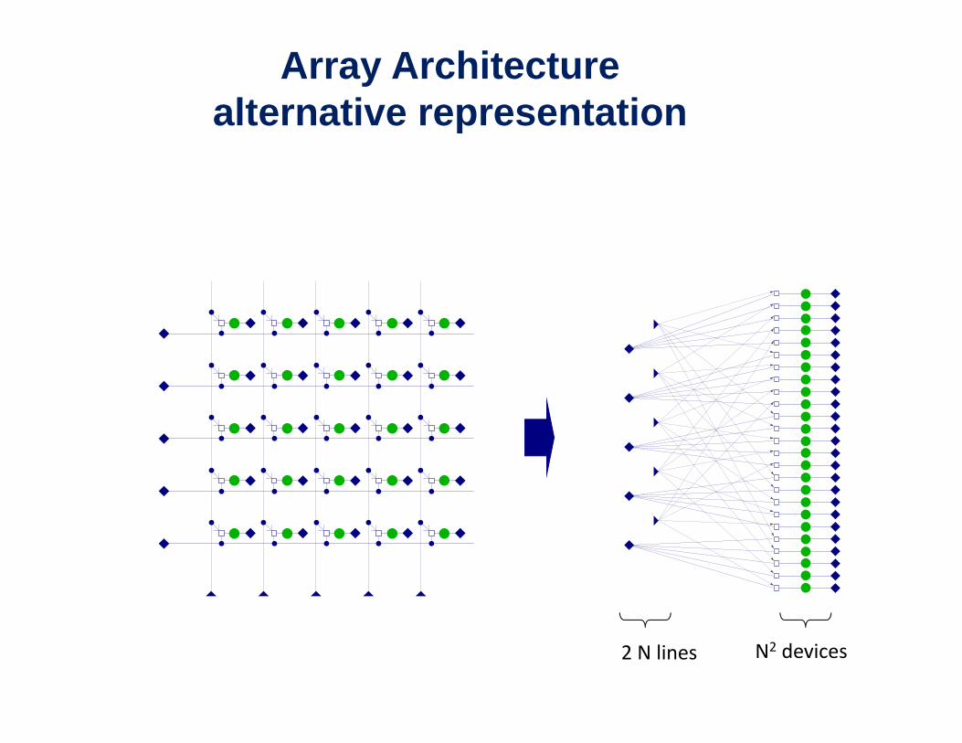
Array Architecturealternative representation
2 N lines N2 devices
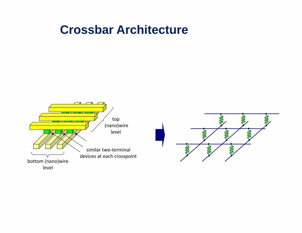
Crossbar Architecture
top(nano)wire
level
bottom (nano)wire
similar two‐terminaldevices at each crosspoint
level
bottom (nano)wire level
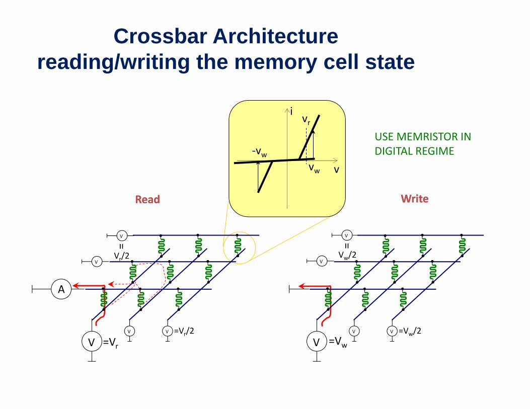
Crossbar Architecturereading/writing the memory cell state
ivr
vvw
‐vwUSE MEMRISTOR INDIGITAL REGIME
ReadRead WriteWrite
V
VVr/2
= V
VVw/2
=
A
V V =Vr/2 V V =Vw/2VV =Vr =Vw
Vr/2 Vw/2
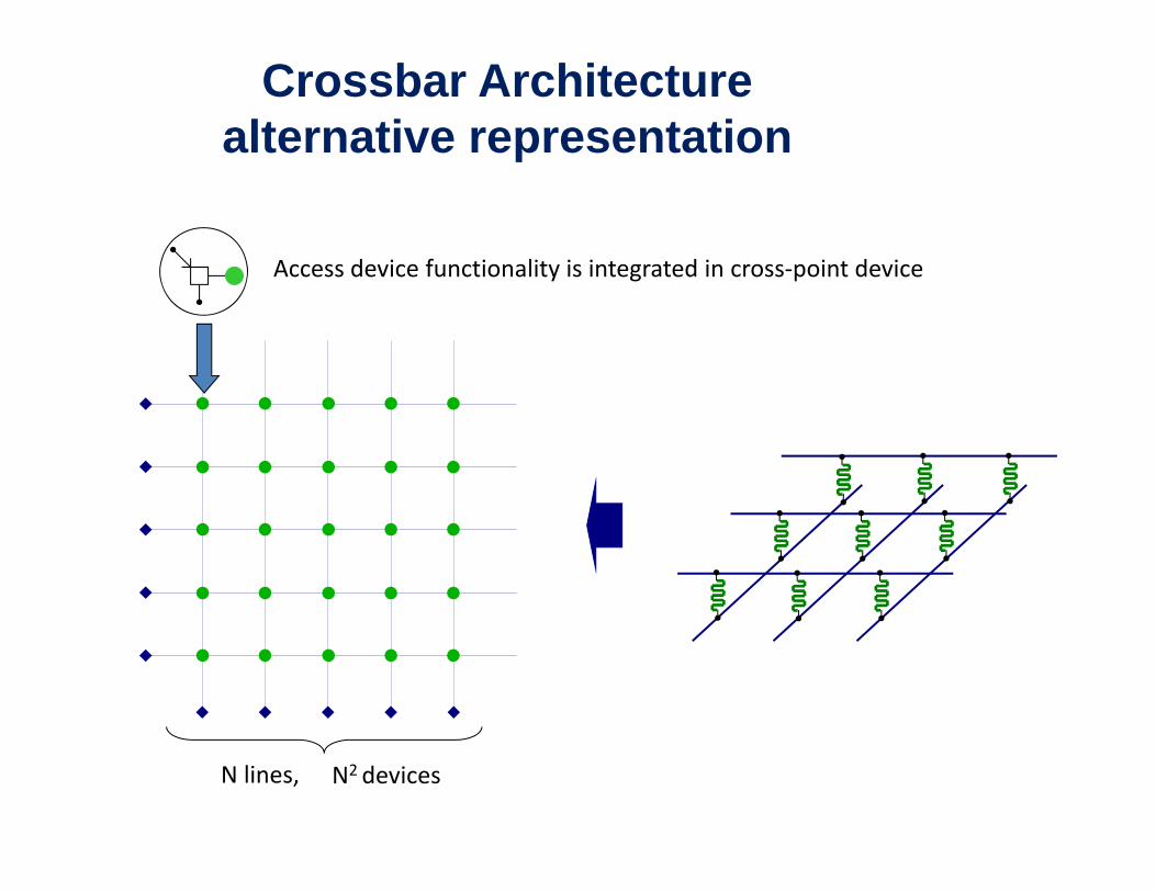
Crossbar Architecturealternative representation
Access device functionality is integrated in cross‐point devicey g p
N lines, N2 devices
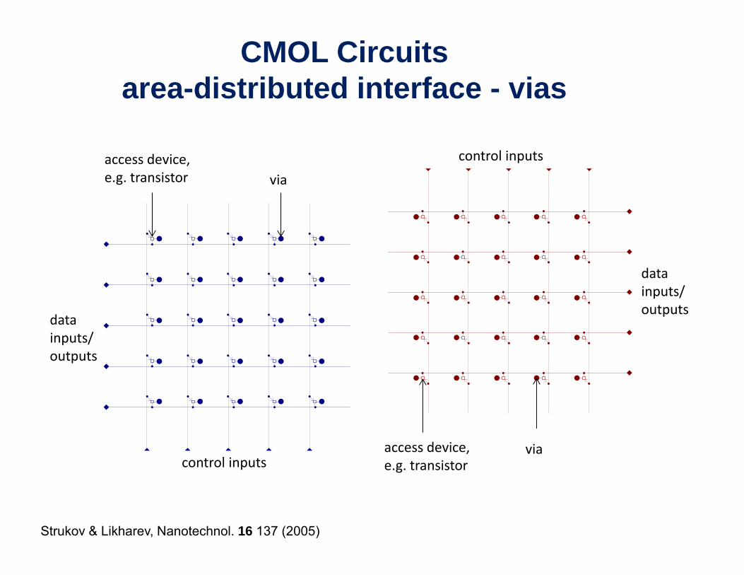
CMOL Circuitsarea-distributed interface - vias
control inputsaccess device, e g transistor viae.g. transistor via
data
datainputs/outputs
datainputs/outputs
control inputsaccess device, e.g. transistor
viap e.g. transistor
Strukov & Likharev, Nanotechnol. 16 137 (2005)
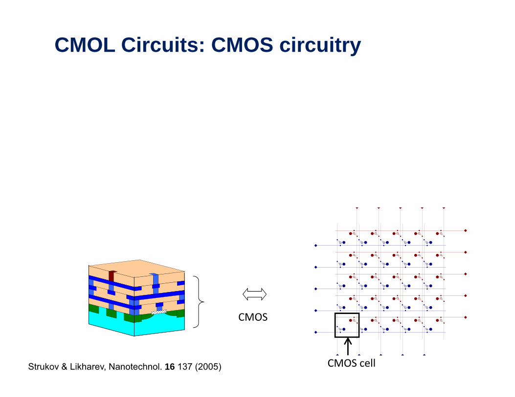
CMOL Circuits: CMOS circuitry
CMOS
CMOS cellStrukov & Likharev, Nanotechnol. 16 137 (2005)
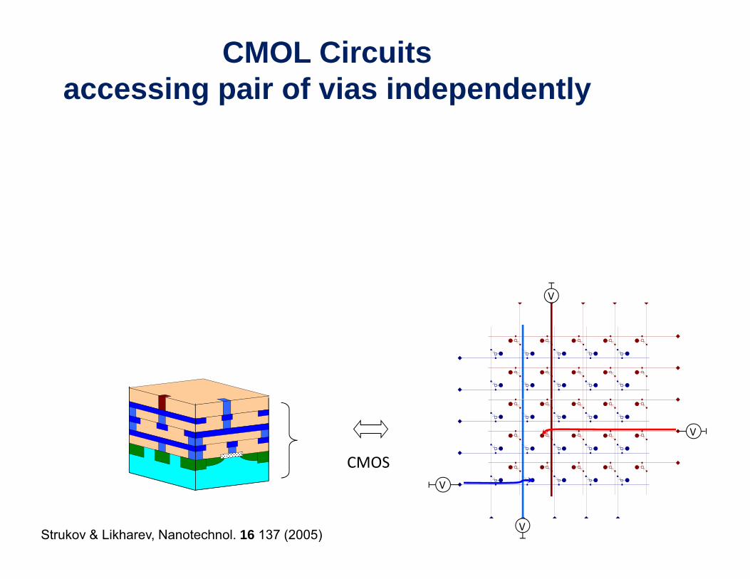
CMOL Circuitsaccessing pair of vias independently
V
CMOS
V
V
V
Strukov & Likharev, Nanotechnol. 16 137 (2005)
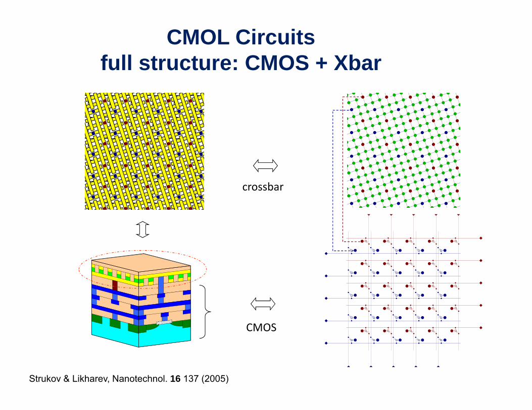
CMOL Circuitsfull structure: CMOS + Xbar
crossbar
CMOS
Strukov & Likharev, Nanotechnol. 16 137 (2005)
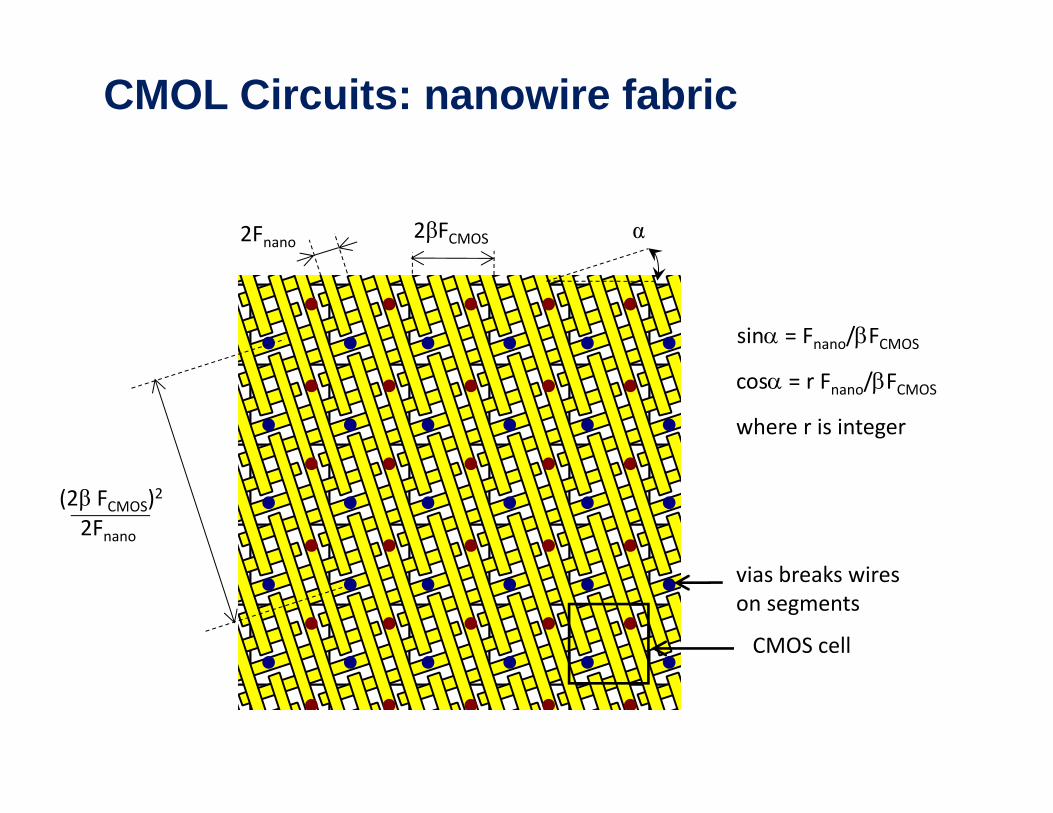
CMOL Circuits: nanowire fabric
2βFCMOS α2Fnano
sin = Fnano/FCMOS
cos = r Fnano/FCMOS
where r is integer
(2β FCMOS)2
2Fnano
vias breaks wires on segments
CMOS cell
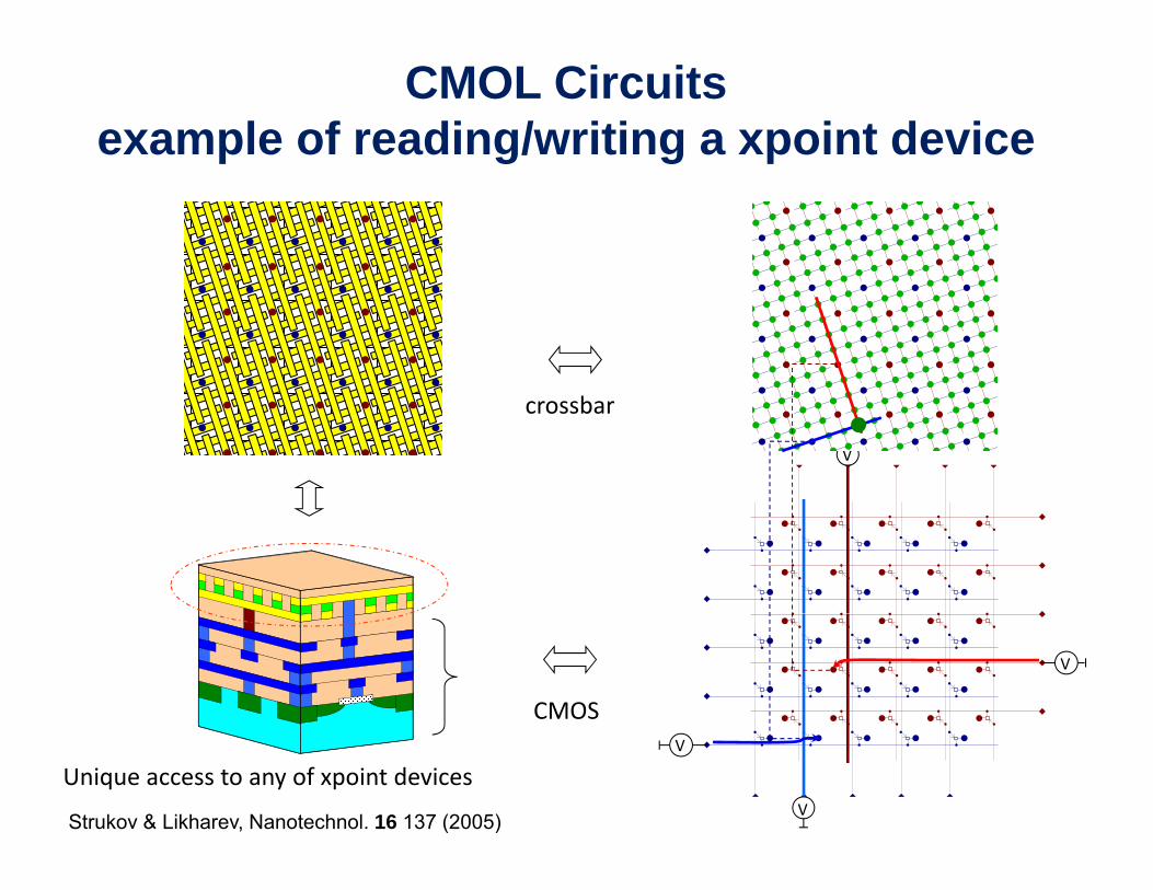
CMOL Circuitsexample of reading/writing a xpoint device
crossbar
V
CMOS
V
V
V
Unique access to any of xpoint devices
Strukov & Likharev, Nanotechnol. 16 137 (2005)
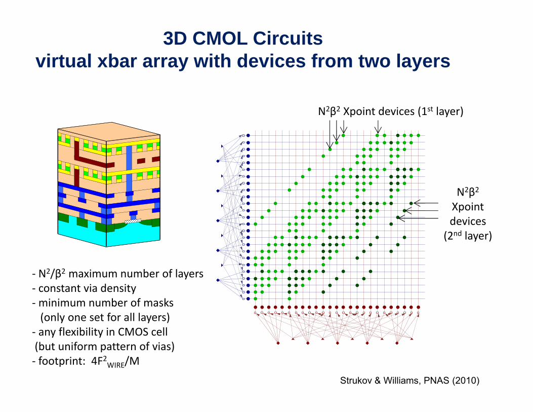
3D CMOL Circuitsvirtual xbar array with devices from two layers
N2β2 Xpoint devices (1st layer)
N2β2
Xpointdevices (2nd l )(2nd layer)
‐ N2/β2 maximum number of layersi d i‐ constant via density
‐minimum number of masks (only one set for all layers)
‐ any flexibility in CMOS cell
Strukov & Williams, PNAS (2010)
y y(but uniform pattern of vias)‐ footprint: 4F2WIRE/M
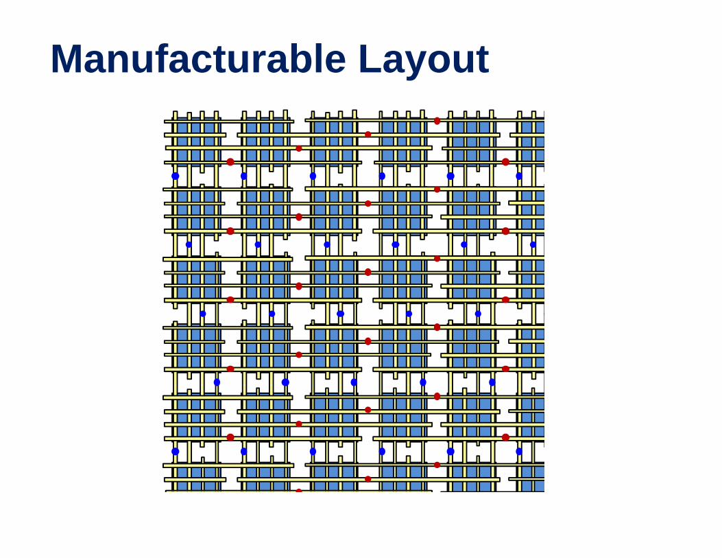
Manufacturable Layout

Di i l M iDigital Memories
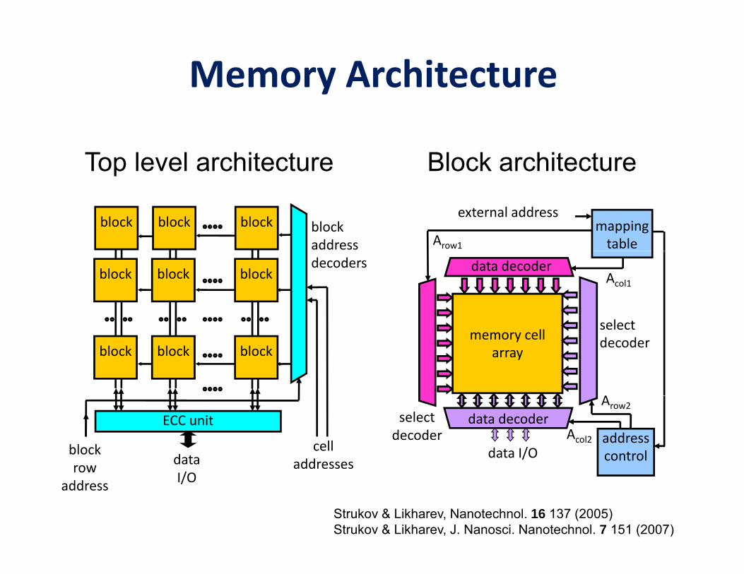
Memory Architecture
Top level architecture Block architecture
block block address
block blockexternal address
mapping tableArow1
decodersblock block block
select
data decoder Acol1
block block block
select decodermemory cell
array
AECC unit
blockrow data
cell addresses
data I/O
selectdecoder address
control
data decoderAcol2
Arow2
rowaddress I/O
addresses
Strukov & Likharev, Nanotechnol. 16 137 (2005)Strukov & Likharev, J. Nanosci. Nanotechnol. 7 151 (2007)
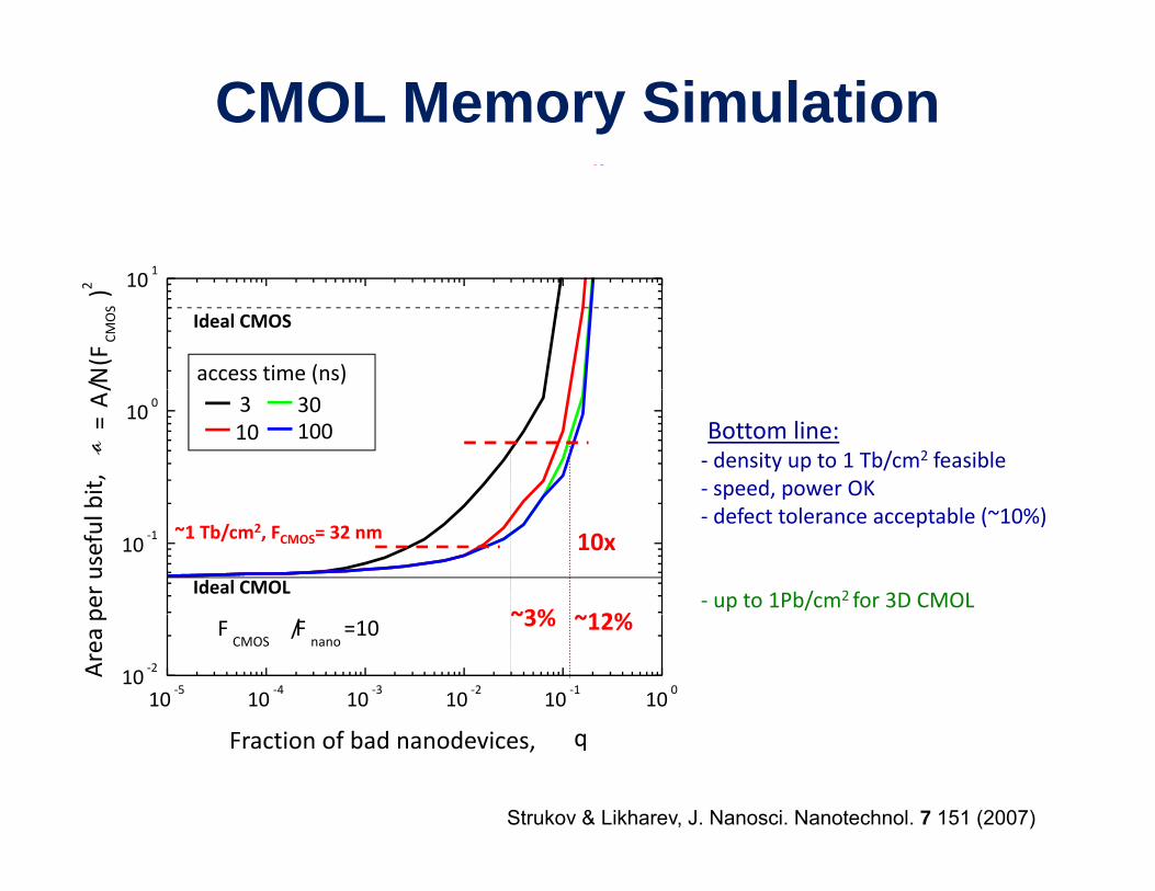
CMOL Memory Simulation
101
10
Ideal CMOS
/N(F
CMOS)2
access time (ns)
10 0
bit,
a= A/
310
30100 Bottom line:
‐ density up to 1 Tb/cm2 feasible‐ speed, power OK
10x
12%~3%
~1 Tb/cm2, FCMOS= 32 nm10‐1
per useful b
Ideal CMOL
‐ defect tolerance acceptable (~10%)
‐ up to 1Pb/cm2 for 3D CMOL~12%~3%
10‐5
10‐4
10‐3
10‐2
10‐1
100
10 ‐2
FCMOS
/Fnano
=10
Area p
Fraction of bad nanodevices, q
Strukov & Likharev, J. Nanosci. Nanotechnol. 7 151 (2007)
FPGA Ci iFPGAs Circuits
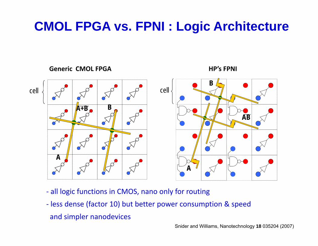
CMOL FPGA vs. FPNI : Logic Architecture
Generic CMOL FPGA HP’s FPNI
BA+B
cellB
cell
BA+BAB
AA
‐ all logic functions in CMOS, nano only for routing
A
‐ less dense (factor 10) but better power consumption & speed
and simpler nanodevicesSnider and Williams, Nanotechnology 18 035204 (2007)
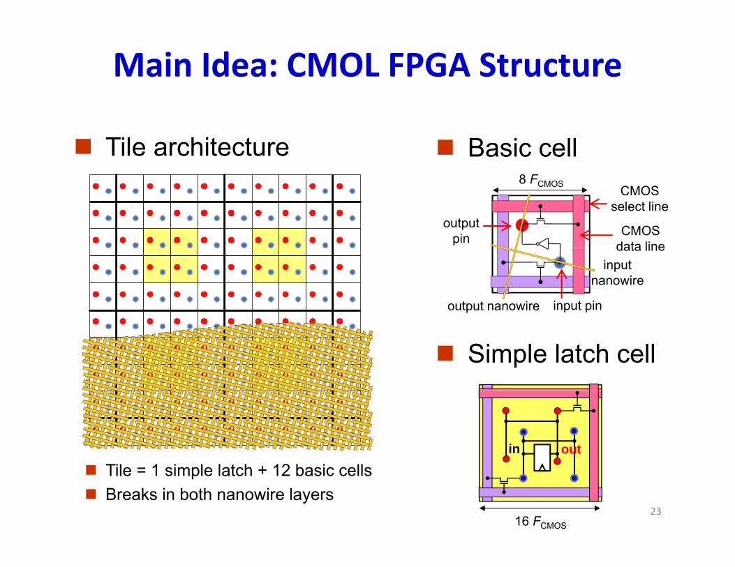
Main Idea: CMOL FPGA Structure
Tile architecture Basic cell8 F
output pin
8 FCMOS CMOS select line
CMOS data line
input nanowire
output nanowire input pin
data line
Simple latch cell
in out
2316 FCMOS
Tile = 1 simple latch + 12 basic cells Breaks in both nanowire layers
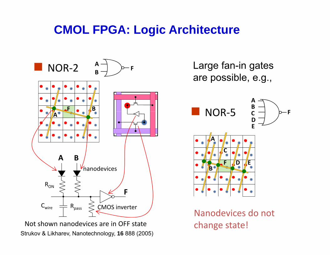
CMOL FPGA: Logic Architecture
NOR‐2 AB
F Large fan-in gates are possible e g
NOR 5AB
FC
are possible, e.g.,
BF NOR‐5 FCDE
A
A
nanodevices
A BB
C
D EF
CMOS inverter
FRON
RpassCwire CMOS inverterRpasswire
Not shown nanodevices are in OFF stateNanodevices do not change state!
Strukov & Likharev, Nanotechnology, 16 888 (2005)
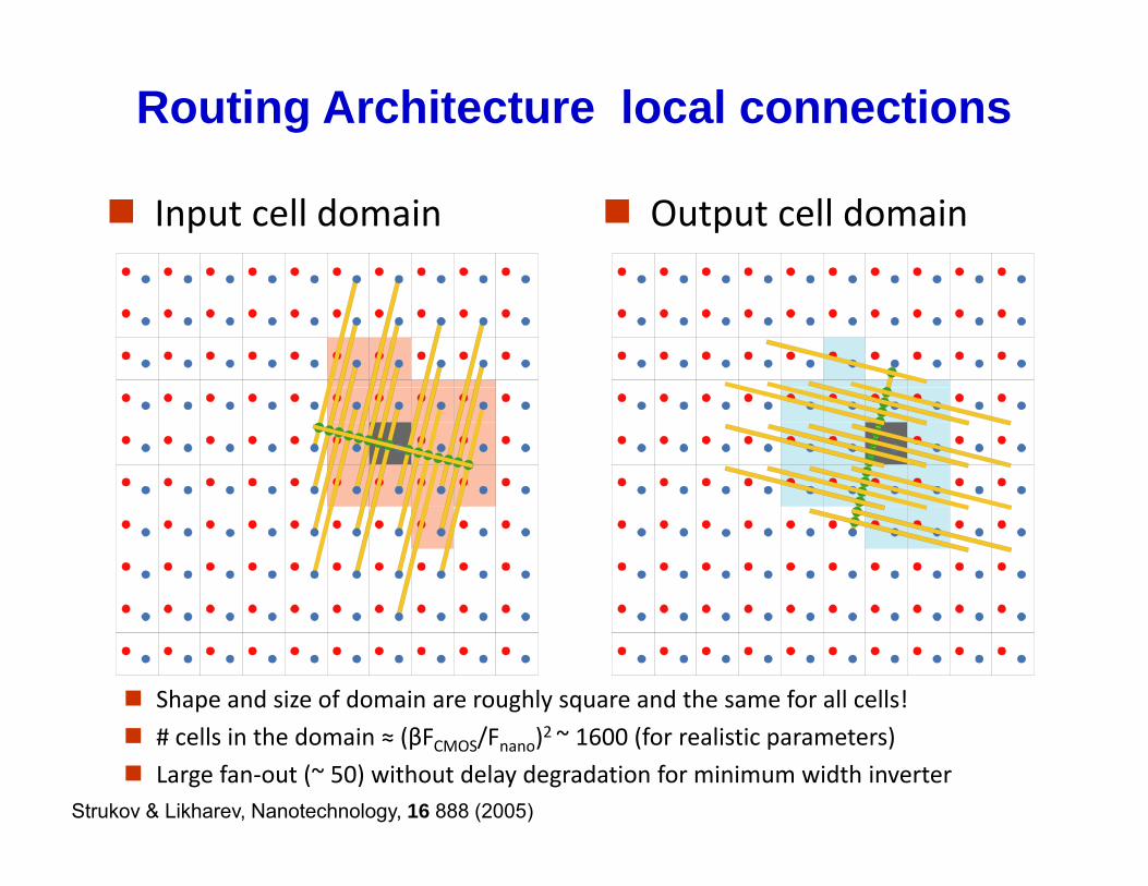
Routing Architecture local connections
Input cell domain Output cell domain
Shape and size of domain are roughly square and the same for all cells!
# cells in the domain ≈ (βFCMOS/Fnano)2 ~ 1600 (for realistic parameters)
Large fan‐out (~ 50) without delay degradation for minimum width inverterStrukov & Likharev, Nanotechnology, 16 888 (2005)
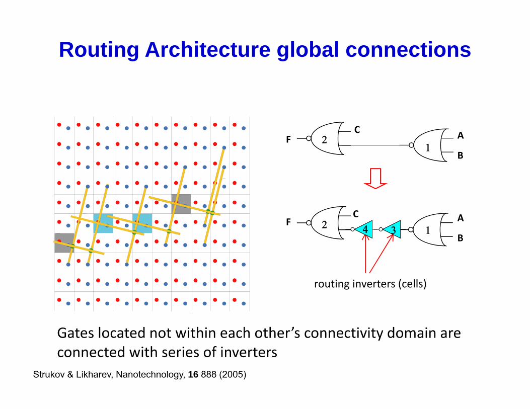
Routing Architecture global connections
C
A
A
B
FC
A
B
C
ACF
F
routing inverters (cells)
B
routing inverters (cells)
Gates located not within each other’s connectivity domain areGates located not within each other s connectivity domain are connected with series of inverters
Strukov & Likharev, Nanotechnology, 16 888 (2005)
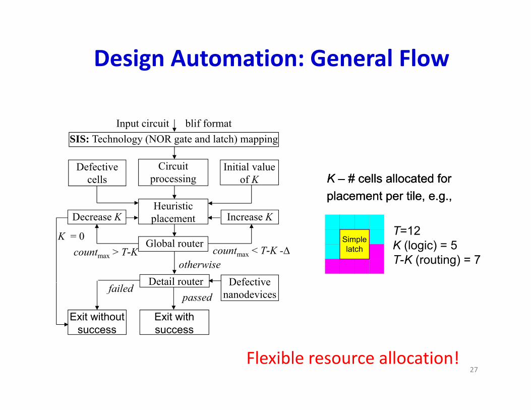
Design Automation: General Flow
Input circuit blif formatSIS: Technology (NOR gate and latch) mapping
p
Initial value of K
Circuit processing
Defective cells KK –– # cells allocated for# cells allocated forof K
Heuristic placement Increase K
processing cells
Decrease KT=12
KK –– # cells allocated for # cells allocated for placement per tile, e.g.,placement per tile, e.g.,
Global routercountmax < T-K -∆countmax > T-K
K = 0
otherwiseDetail router Defective
Simplelatch
T=12K (logic) = 5T-K (routing) = 7
Exit with success
Exit without success
Detail router Defective nanodevicesfailed
passed
27Flexible resource allocation!
Step 1: Technology MappingStep 1: Technology Mapping
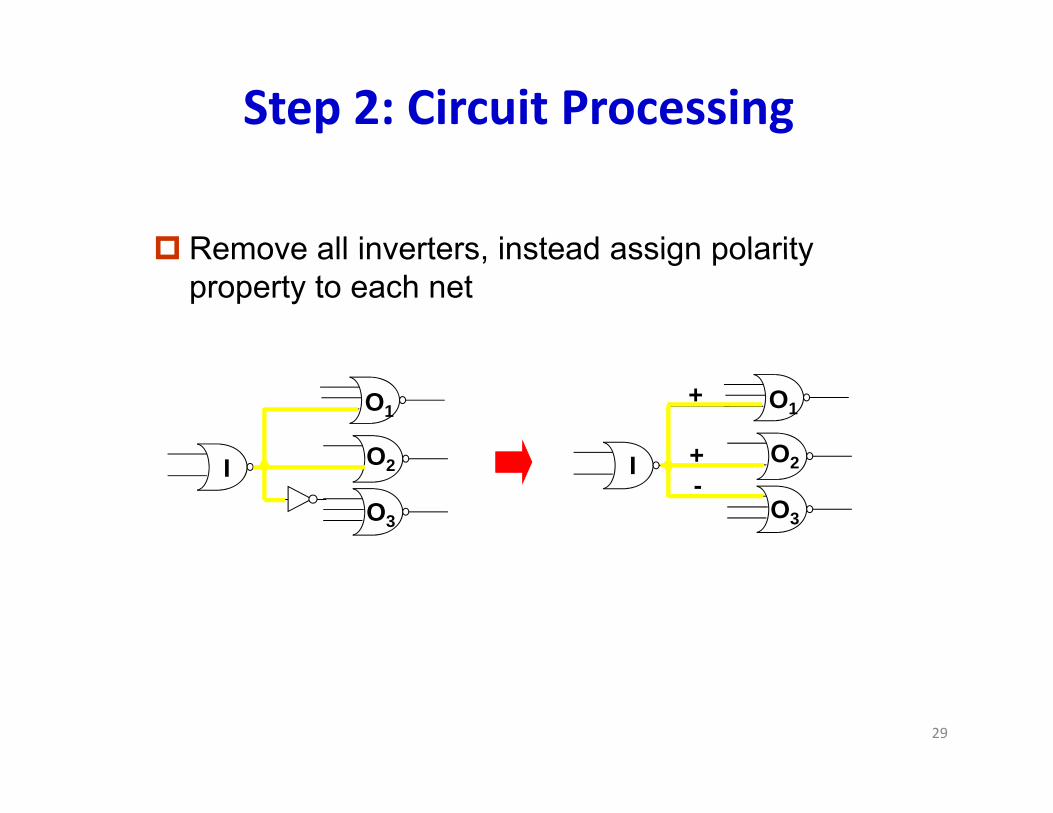
Step 2: Circuit Processing
Remove all inverters instead assign polarity Remove all inverters, instead assign polarity property to each net
O1
O
+
+I
O1
O2I O2
O3
-+I O2
O3
29
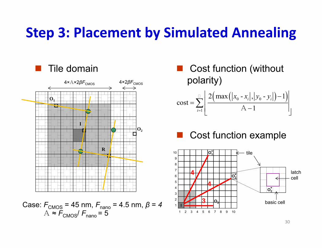
Step 3: Placement by Simulated Annealing
Tile domain Cost function (without l it )4×A×2βFCMOS
O1
4×2βFCMOS
0 02 max - , - 1cost
1i ix x y y
A
polarity)
IO2
1 1i A
Cost function exampleO1
9
10
8
7
tile
4
+R
l t h
p
O2
O3
7
6
4
5
3
2
4
4
3
+
O2+
basic cell
latch cell
C F 45 F 4 5 β 4
30
O3I
6 7 8 9 101 2 3 4 5
13 - basic cellCase: FCMOS = 45 nm, Fnano = 4.5 nm, β = 4
A ≈ FCMOS/ Fnano = 5
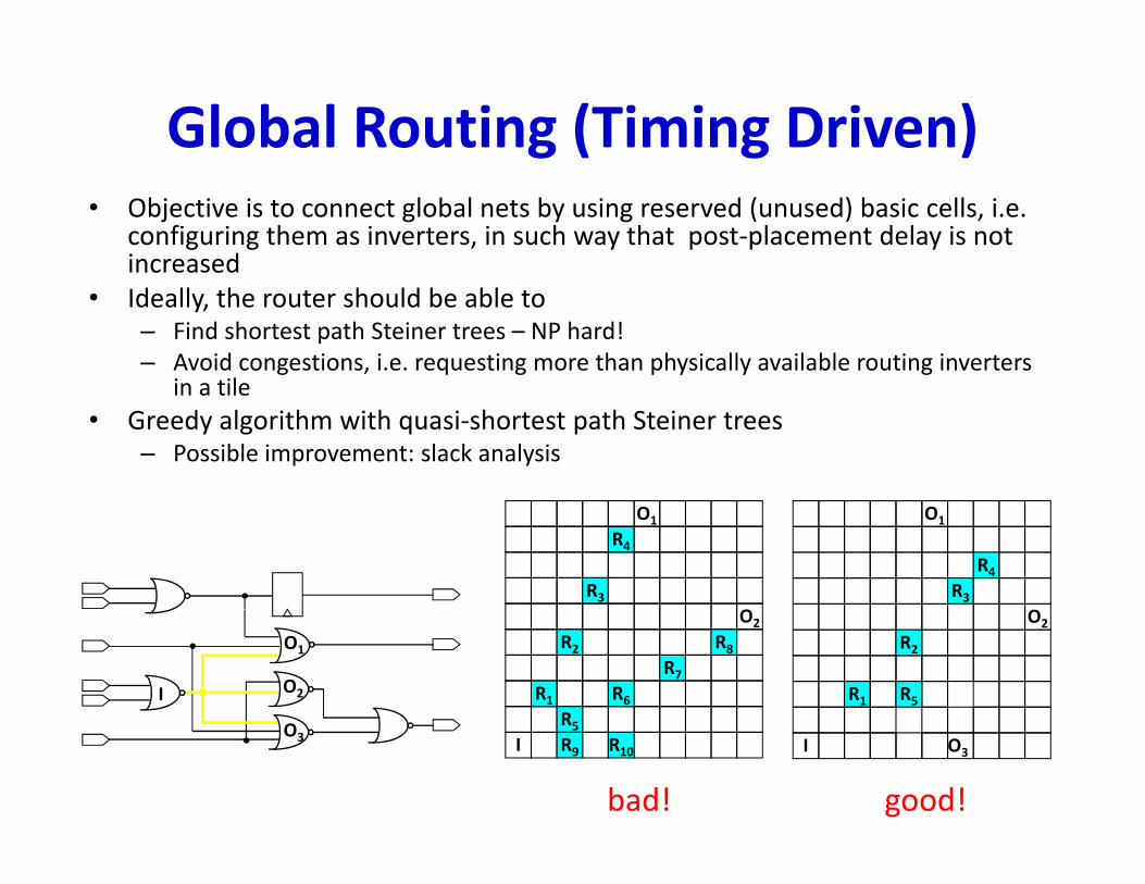
Global Routing (Timing Driven) • Objective is to connect global nets by using reserved (unused) basic cells, i.e.
configuring them as inverters, in such way that post‐placement delay is not increased
• Ideally, the router should be able to – Find shortest path Steiner trees – NP hard!– Avoid congestions, i.e. requesting more than physically available routing inverters
in a tilein a tile• Greedy algorithm with quasi‐shortest path Steiner trees
– Possible improvement: slack analysis
R4
R3
O1
O
O1
R4
R3
O2
R7
R8R2
R1 R6
R
O2
R2
R1 R5I
O1
O2
R5
I R9 R10 O3IO3
bad! good!
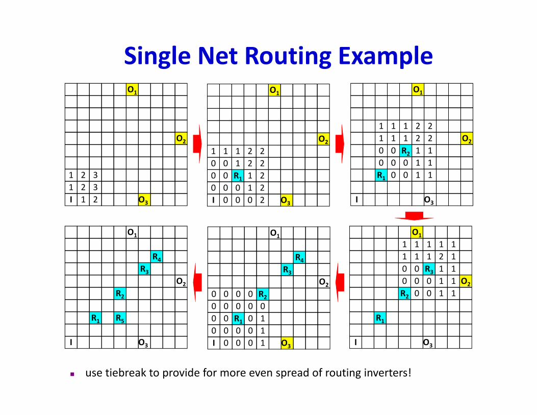
Single Net Routing ExampleO1 O1
1 1 1
O1
2 2O2
1 2 3
O2
0 0 1 2 21 1 1 2 2
0 0 R1 1 2
1 1 1 2 2 O2
1 11 1
1 10 0 00 0 R2
R1 0 0
O1
O3
1 2 3I 1 2 O3
0 0 0 1 2I 0 0 0 2 O3I
OO1
1100
1 1 1 1O1
1 1 2 10 R3 1 10 0 1 1 O2
O1
R4
R3
O2
O1
R4
R3
O2 2
0 0 1 1R2
R1
2
0 0 0 0 00 0 0 0 R2
0 0 R1 0 10 0 0 0 1
2
R2
R1 R5
O3IO3I 0 0 0 1O3I
use tiebreak to provide for more even spread of routing inverters!
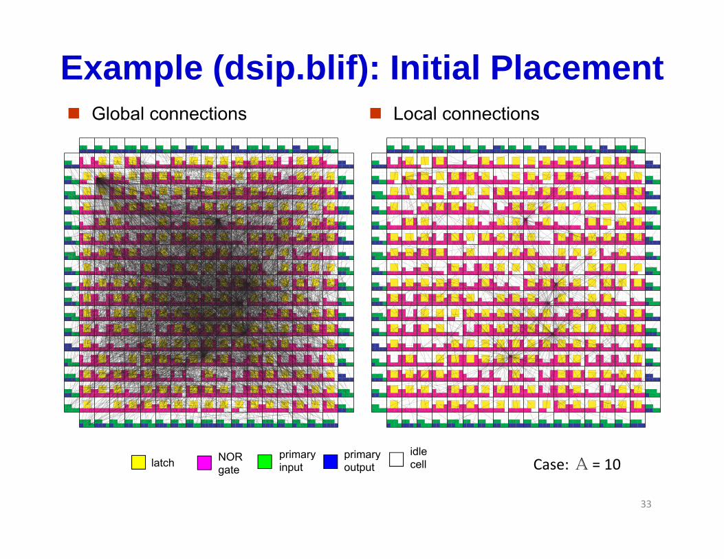
Example (dsip.blif): Initial Placement Global connections Local connections
primaryNOR primary idle
33
latchprimary input
NOR gate
primary output cell Case: A = 10
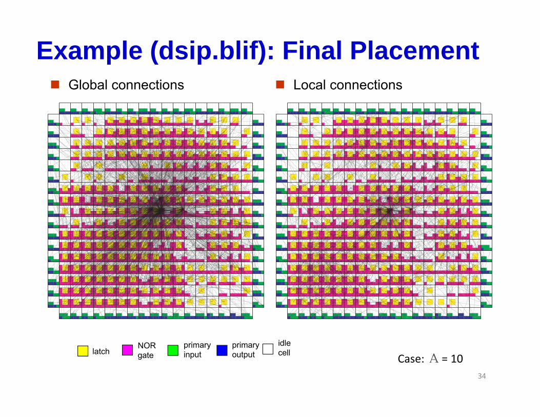
Example (dsip.blif): Final Placement Global connections Local connections
idl
34
latchprimary input
NOR gate
primary output
idlecell
Case: A = 10
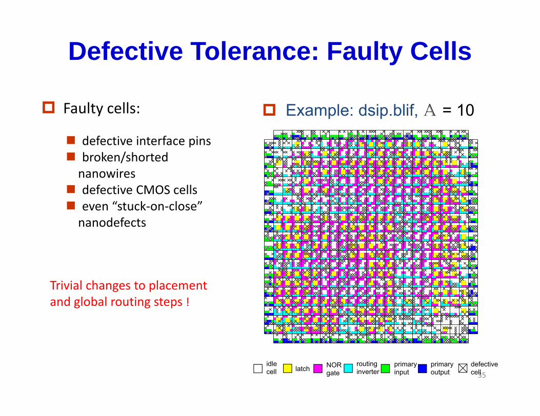
Defective Tolerance: Faulty Cells
Example: dsip.blif, A = 10 Faulty cells:
defective interface pins broken/shorted nanowires
defective CMOS cells even “stuck‐on‐close”nanodefects
Trivial changes to placementTrivial changes to placement and global routing steps !
35latch
primary input
NOR gate
routing inverter
primary output
defective cell
idlecell
Step 4: Global routing Objective is to connect global nets by using reserved (unused) basic
cells, i.e. configuring them as inverters, in such way that post-placement delay is not increasedy
Ideally, the router should be able to Find shortest path Steiner trees – NP hard! Avoid congestions, i.e. requesting more than physically available routing
inverters in a tileinverters in a tile Greedy algorithm with quasi-shortest path Steiner trees
R4
R3
O1
O
O1
R4R3
O
+ +
+ +O2
R7
R8R2
R1 R6R
O2R2
R1 R5I
O1
O2
+ +
+
+‐
36
O3
R5I R9 R10 O3I
O3 ‐ ‐
Single Net Global RoutingO1 O1
1 1 1
O1
2 2
a) b) c)+ + +
O2
2 3 3
2 3 3
O2
0 0 2 3 3
1 1 2 3 3
0 0 R1 2 2
1 1 1
1 1 1
2 2
2 2 O2
1 1
1 1
2 2
0 0 0
0 0 R2
R1 0 1
+ + +
O3
2 3 3
I 2 2 O3
0 0 1 1 2
I 0 1 1 2
O1
O3I
O1O1 e)f)g) +++
- - -
1
1
0
0
1 1 1 1
1 1 2 1
0 R3 1 1
0 0 1 1 O2
0 0 1 1R2
0 0 0
0 0 0
R4
0 R3
0 0 O2
0 00 0 R2
R4
R3
O2
R2
+++
O3
2
R1
I
0 0
0 0
1 1
O3
0 0 0
0 0 2
R1 0 1
IO3
2
R1 R5
I---
37not always optimal !
Example (dsip.blif): Global Routing Global connections Local connections
primaryNOR routing i idle
38
latch primary input
NOR gate
routing inverter
primary output
idlecell Case: A = 10
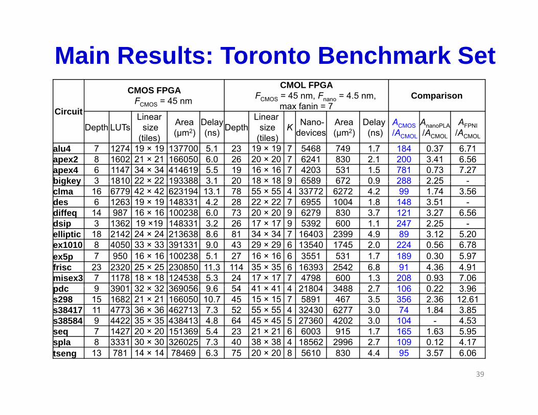
Main Results: Toronto Benchmark Set
Circuit
CMOS FPGA FCMOS = 45 nm
CMOL FPGA FCMOS = 45 nm, Fnano = 4.5 nm,
max fanin = 7Comparison
Depth LUTsLinear
size Area2
Delay DepthLinear
size K Nano- Area2
Delay ACMOS AnanoPLA AFPNIDepth LUTs size (tiles) (μm2) (ns) Depth size
(tiles) K devices (μm2) (ns) /ACMOL /ACMOL /ACMOL
alu4 7 1274 19 × 19 137700 5.1 23 19 × 19 7 5468 749 1.7 184 0.37 6.71apex2 8 1602 21 × 21 166050 6.0 26 20 × 20 7 6241 830 2.1 200 3.41 6.56apex4 6 1147 34 × 34 414619 5.5 19 16 × 16 7 4203 531 1.5 781 0.73 7.27bigkey 3 1810 22 × 22 193388 3 1 20 18 × 18 9 6589 672 0 9 288 2 25 -bigkey 3 1810 22 × 22 193388 3.1 20 18 × 18 9 6589 672 0.9 288 2.25 -clma 16 6779 42 × 42 623194 13.1 78 55 × 55 4 33772 6272 4.2 99 1.74 3.56des 6 1263 19 × 19 148331 4.2 28 22 × 22 7 6955 1004 1.8 148 3.51 -diffeq 14 987 16 × 16 100238 6.0 73 20 × 20 9 6279 830 3.7 121 3.27 6.56dsip 3 1362 19 ×19 148331 3.2 26 17 × 17 9 5392 600 1.1 247 2.25 -elliptic 18 2142 24 × 24 213638 8 6 81 34 × 34 7 16403 2399 4 9 89 3 12 5 20elliptic 18 2142 24 × 24 213638 8.6 81 34 × 34 7 16403 2399 4.9 89 3.12 5.20ex1010 8 4050 33 × 33 391331 9.0 43 29 × 29 6 13540 1745 2.0 224 0.56 6.78ex5p 7 950 16 × 16 100238 5.1 27 16 × 16 6 3551 531 1.7 189 0.30 5.97frisc 23 2320 25 × 25 230850 11.3 114 35 × 35 6 16393 2542 6.8 91 4.36 4.91misex3 7 1178 18 × 18 124538 5.3 24 17 × 17 7 4798 600 1.3 208 0.93 7.06
d 9 3901 32 32 369056 9 6 54 41 41 4 21804 3488 2 7 106 0 22 3 96pdc 9 3901 32 × 32 369056 9.6 54 41 × 41 4 21804 3488 2.7 106 0.22 3.96s298 15 1682 21 × 21 166050 10.7 45 15 × 15 7 5891 467 3.5 356 2.36 12.61s38417 11 4773 36 × 36 462713 7.3 52 55 × 55 4 32430 6277 3.0 74 1.84 3.85s38584 9 4422 35 × 35 438413 4.8 64 45 × 45 5 27360 4202 3.0 104 - 4.53seq 7 1427 20 × 20 151369 5.4 23 21 × 21 6 6003 915 1.7 165 1.63 5.95
39
spla 8 3331 30 × 30 326025 7.3 40 38 × 38 4 18562 2996 2.7 109 0.12 4.17tseng 13 781 14 × 14 78469 6.3 75 20 × 20 8 5610 830 4.4 95 3.57 6.06
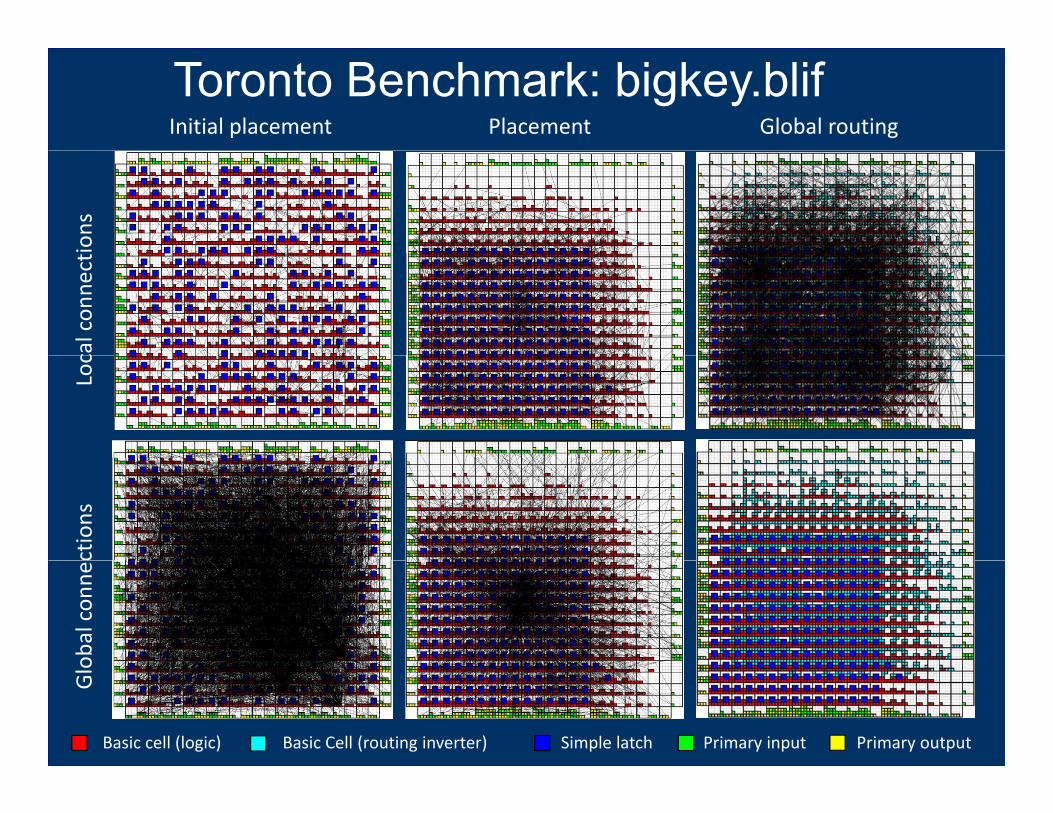
Toronto Benchmark: bigkey.blifInitial placement Placement Global routing
ions
cal con
nect
Loc
ctions
obal con
ne
Primary outputPrimary inputBasic cell (logic) Simple latchBasic Cell (routing inverter)
Glo
CMOL DSP: convolution example
CMOL DSP: ~ 25 μs per frameT
‐window
1 1
STF F
μ p
Aggressively scaled CELL (45 nm): 3.5 ms
N
F
Splane
pixel(output)
1,0
,,0 0
,,
FNyx
ST jii j
jyixyx
S 12 bits o
ut
out
out
in
in
in
φ (12 bits)
msF
(input)
CMOL pixel mappingφ (12 bits)
12‐bit Wallace Tree Multiplier (Partial Product Generation and
Reduction)
12 bits
cA
cB0 1
1 0
Programmable latch cell
Control cellusednot used
32‐bit Kogge Stone Adder
out
out
out
in
in
in
M24 bits
1
20
c
24 bits
A 1 0
0
multiplierdd
used
not used
Basic cell
out
out
out
in
in
in
T32 bits
1
0
cT
M 32 bits
addermultiplexerothernot used
D. B. Strukov and K. K. Likharev, Tran. IEEE Nanotechnol. 7 151 (2007)
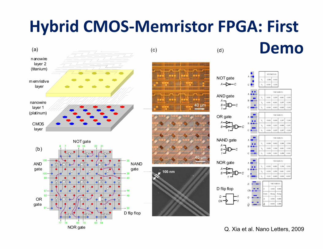
Hybrid CMOS‐Memristor FPGA: First DemoDemo (c) (d) (a)
n anowire layer 2
(titanium) NOT gate
nanowire layer 1
m emristive layer
AND gate
NOT gate
CMOS layer
aye (platinum)
NOT t NAND gate
OR gate
(b )
AND gate
NOT gate
NAND gate
NOR gate
NAND gate
OR t
D flip flop
Q. Xia et al. Nano Letters, 2009
gate
NOR gate
D flip flop
Pattern matchingPattern matching
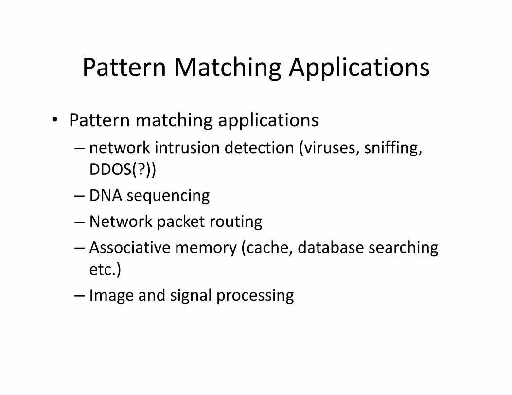
Pattern Matching ApplicationsPattern Matching Applications
• Pattern matching applicationsPattern matching applications– network intrusion detection (viruses, sniffing, DDOS(?))DDOS(?))
– DNA sequencing
– Network packet routing– Network packet routing
– Associative memory (cache, database searching etc )etc.)
– Image and signal processing
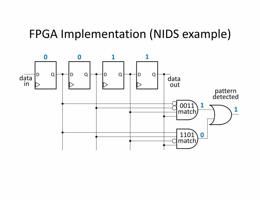
FPGA Implementation (NIDS example)FPGA Implementation (NIDS example)
0 0 1 1
D Q D Q D Q D Qdata in
data out
0011match
1
patterndetected
1match
1101 0match
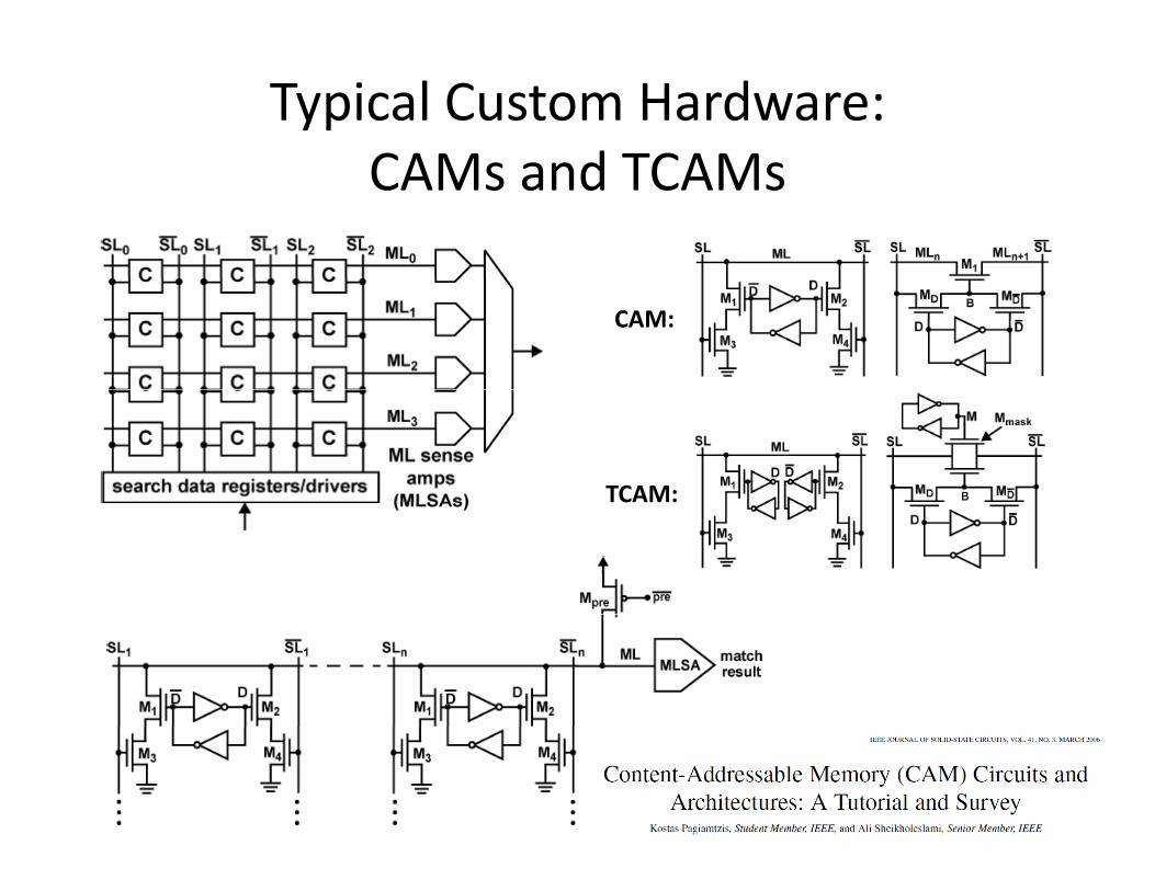
Typical Custom Hardware: CAMs and TCAMsCAMs and TCAMs
CAM:
TCAM:TCAM:
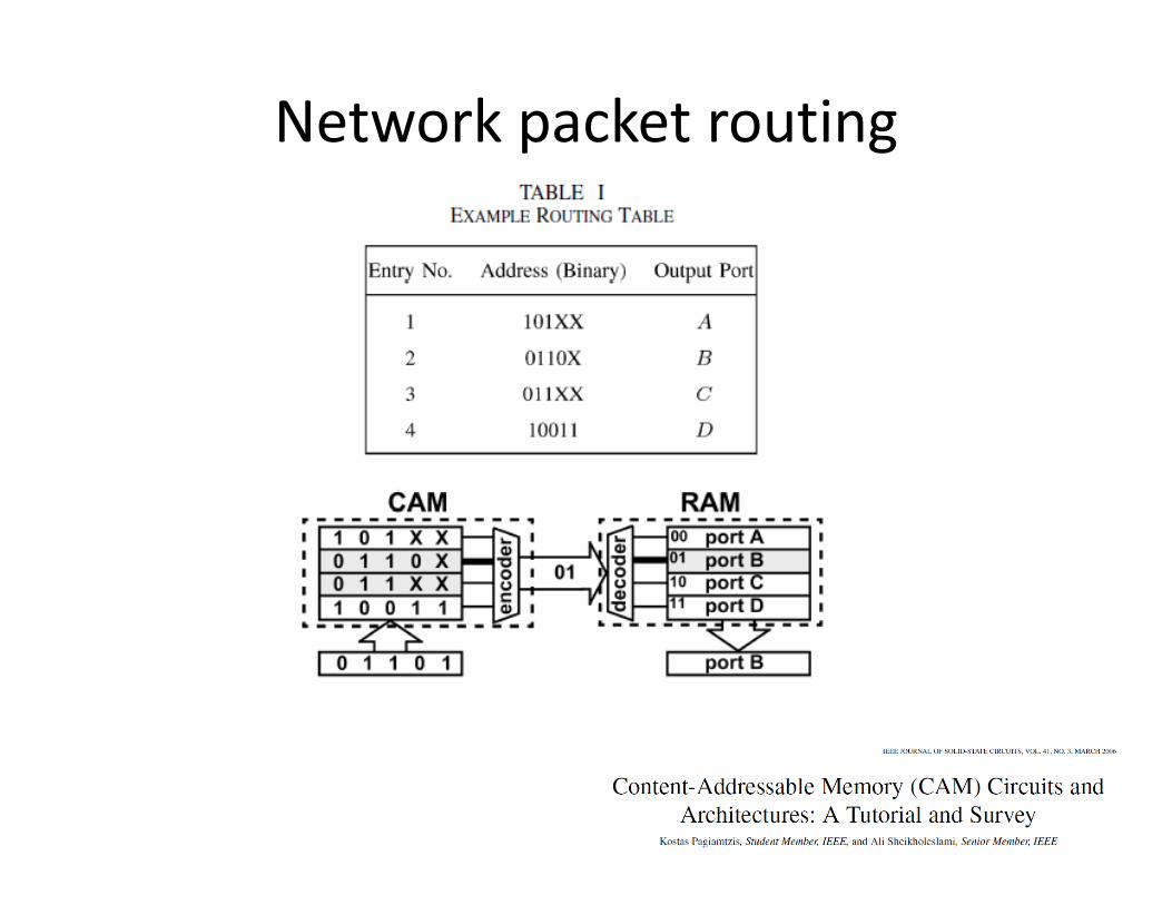
Network packet routing
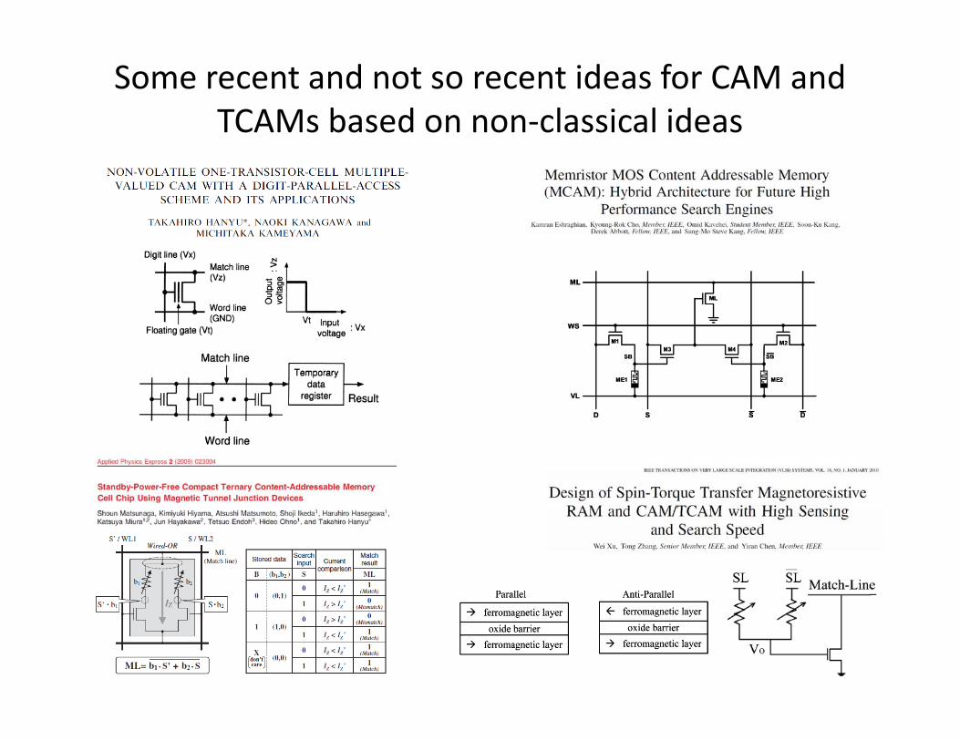
Some recent and not so recent ideas for CAM and TCAMs based on non‐classical ideas
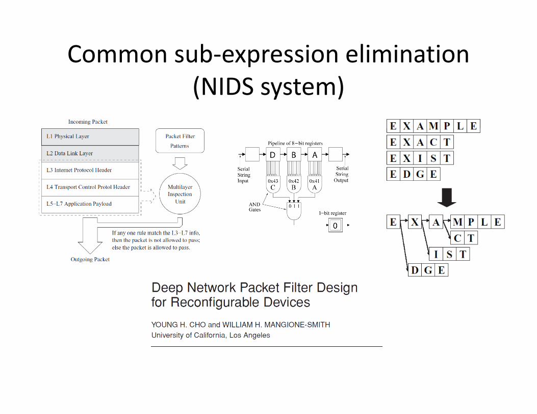
Common sub‐expression elimination ( )(NIDS system)
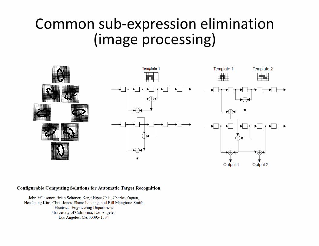
Common sub‐expression elimination (image processing)( g p g)
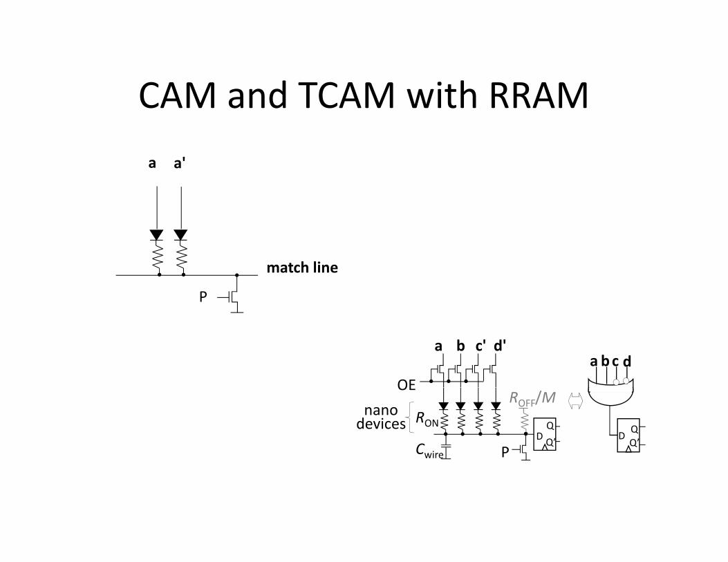
CAM and TCAM with RRAMCAM and TCAM with RRAM
a a'
match line
P
a b c'
OE
d'a bc d
RON
Cwire
ROFF/M
DQ
Q’
OE
P
nanodevices
DQQ’

Basic Idea ofBasic Idea of
• Diode like TCAM cells (high density)Diode like TCAM cells (high density)
• CMOL FPGA architecture (low overhead for configuration high integration bandwidthconfiguration, high integration bandwidth with crossbars)
O h d f 3D ki• Overhead free 3D stacking
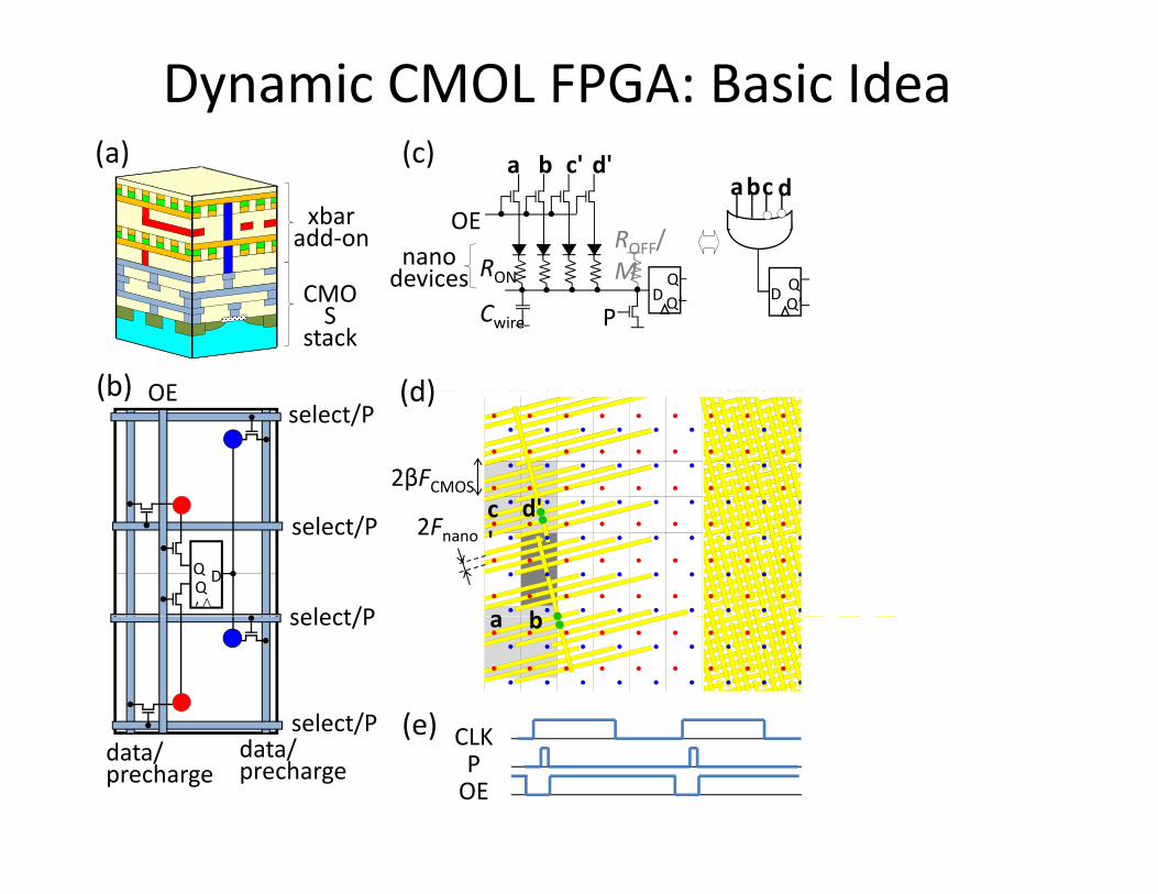
(a) (c) a b c' d'
Dynamic CMOL FPGA: Basic Idea
xbaradd‐on
( ) ( ) a
RON
b c
ROFF/M Q
OEnanodevices
dabc d
CMOS
stack
(d)(b) OE
ON
Cwire
MDQQ’
P
devicesD QQ’
2βFCMOS
(d)(b)select/P
OE
d'2Fnano
DQQ’ a b
c'
d'select/P
select/P
CLK(e)
a bselect/P
select/P CLKPOE
data/precharge
(e)select/Pdata/precharge
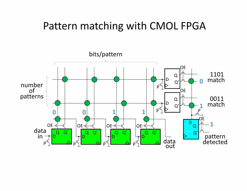
Pattern matching with CMOL FPGA
bits/pattern
01101match
bD
QQ’
OE
1
0
0011match
number of
patternsD
QQ’
QP
OE
data
111
0 0
1Q Q’ Q Q’ Q Q’
Q
DQQ’
P P
Q Q’OE OE OE OE
OE
data in
data out
patterndetected
DQ Q’
DQ Q’
DQ Q’ Q’
PPPPDQ Q’
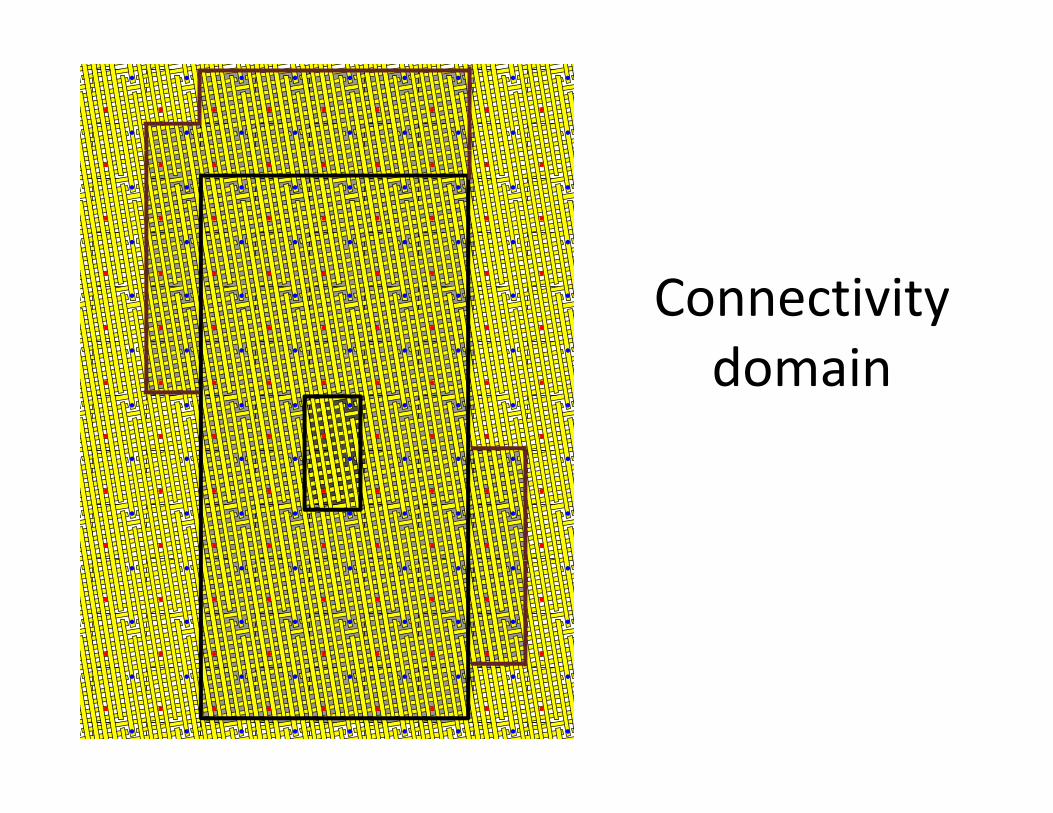
Connectivity d idomain
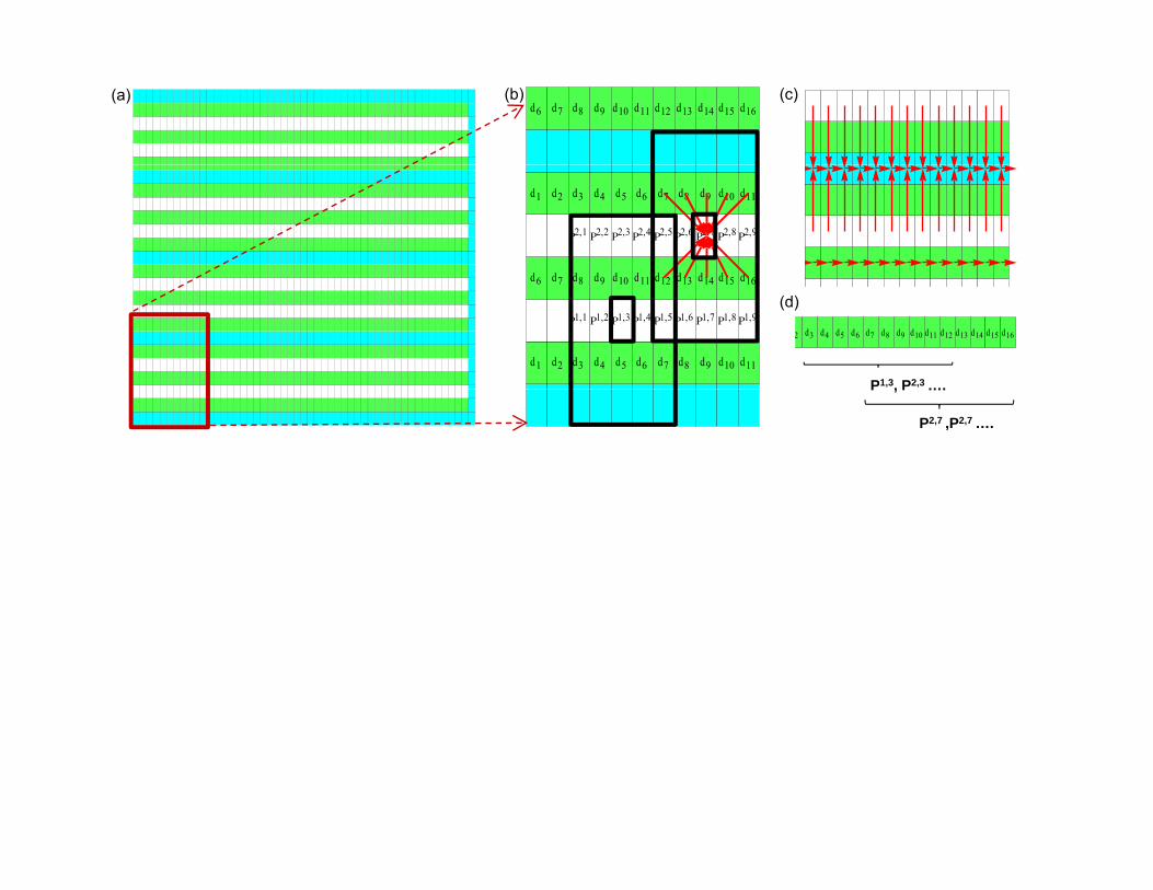
d6 d7 d8 d9 d10 d11 d12 d13 d14 d15 d16(a) (b) (c)
d d d d d d d d d d d
R2,1 R2,2 R2,3 R2,4 R2,5 R2,6 R2,7 R2,8 R2,9
d1 d2 d3 d4 d5 d6 d7 d8 d9 d10 d11
d1 d2 d3 d4 d5 d6 d7 d8 d9 d10 d11
R1,1 R1,2 R1,3 R1,4 R1,5 R1,6 R1,7 R1,8 R1,9
d6 d7 d8 d9 d10 d11 d12 d13 d14 d15 d16
P1,3, P2,3 ….
(d)
2 d3 d4 d5 d6 d7 d8 d9 d10 d11 d12 d13 d14 d15 d16
P , P ….
P2,7 ,P2,7 ….
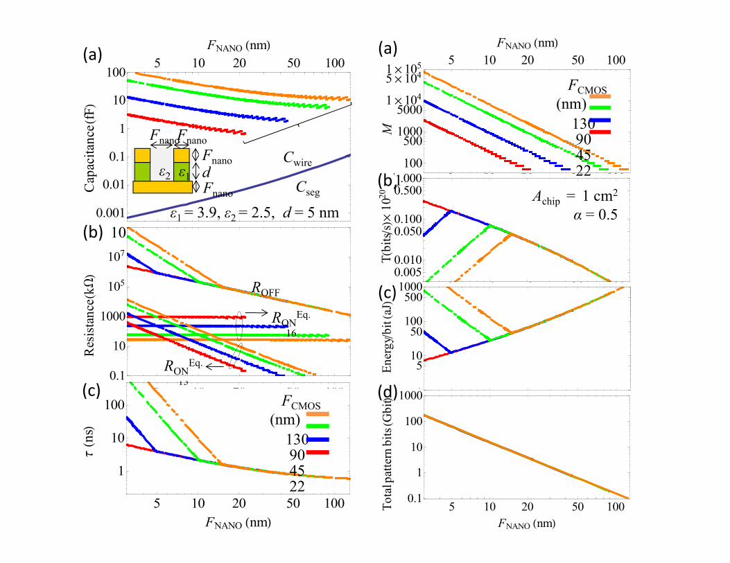
1μ104
5μ1041μ105 5 10 20 50 100FNANO nm(a)
FCMOS (nm)10
1005 10 20 50 100
FNANO nm(a)
100
5001000
50001μ10
1 0005 10 20 50 100
M
(b)
(nm)1309045221
0.1
1
10pa
cita
nce
fF
Cwireε2 ε1 dFnano
FnanoFnano
0.0500.100
0.5001.000
bits
sμ10
20
(b) 22Achip = 1 cm2
α = 0.5
1
0.001
0.01
10910
Cap
(b)
Cseg
ε2 ε1 dFnano
ε1 = 3.9, ε2 = 2.5, d = 5 nm
5 10 20 50 1000.0050.010
FNANO nm100
5001000
5 0 0 50 00
Tb
aJ(c)
1000
105
107
ncek
W
ROFF
R Eq.
1
510
50100
Ener
gyb
it
(d)5 10 20 50 1000.1
10
1000
Res
ista
n
(c)
RONEq.
16
RONEq.
131
10
100
10005 10 20 50 100
ern
bits
Gbi
t(d)5 10 20 50 100FNANO nm
10
100
tn
s
(c) FCMOS (nm)
13090
5 10 20 50 1000.1
1
FNANO nm
Tota
lpat
te
5 10 20 50 100
1
FNANO nm
904522