novel dual-band ltcc bandpass filters for microwave
TRANSCRIPT

Novel Dual-band LTCC Bandpass Filters for MicrowaveApplications
by
Aref POURZADI
MANUSCRIPT-BASED THESIS PRESENTED TO ÉCOLE DE
TECHNOLOGIE SUPÉRIEURE IN PARTIAL FULFILLMENT OF THE
DEGREE OF DOCTOR OF PHILOSOPHY
Ph.D.
MONTREAL, "MARCH 29TH, 2020"
ÉCOLE DE TECHNOLOGIE SUPÉRIEUREUNIVERSITÉ DU QUÉBEC
Aref Pourzadi, 2020

It is forbidden to reproduce, save or share the content of this document either in whole or in parts. The reader
who wishes to print or save this document on any media must first get the permission of the author.

BOARD OF EXAMINERS
THIS THESIS HAS BEEN EVALUATED
BY THE FOLLOWING BOARD OF EXAMINERS
Prof. Ammar Kouki, Thesis Supervisor
Department of Electrical Engineering, École de technologie superieure
Prof. Nicole Demarquette, President of the Board of Examiners
Department of Mechanical Engineering, École de Technologie Superieure
Prof. Jean-Marc Lina, Member of the jury
Department of Electrical Engineering, École de Technologie Superieure
Prof. Tayeb A.Denidni, External Examiner
Énergie Matériaux Télécommunications Research Centre, Institut National de la Recherche
Scientifique
THIS THESIS WAS PRESENTED AND DEFENDED
IN THE PRESENCE OF A BOARD OF EXAMINERS AND THE PUBLIC
ON "FEBRUARY 19TH, 2020"
AT ÉCOLE DE TECHNOLOGIE SUPÉRIEURE


FOREWORD
This thesis is written as completion to Ph.D. in electrical engineering, at École de Technologie
Superieure (ÉTS). Author worked on the subject since May 2014 to November 2019. The
content is the original work of its author Aref Pourzadi.


ACKNOWLEDGEMENTS
I would like to take this opportunity expressing thank all people who have made this journey
memorable.
First and foremost, I would like to express my sincere gratitude to my supervisior Prof. Ammar
Kouki for giving me this opportunity. Not only for guiding and teaching me during my study,
but also I appreciate him so much for all of his supports in my non-academic life.
Secondly, I would like to thank my Ph.D. committee members, Professors Nicole Demarquette,
Jean-Marc Lina, and Tayeb A.Denidni for spending their time to read this thesis and giving me
their valuable comments and feedbacks. Next, I am grateful to our technical staff, Normand
Gravel, for the uncountable help he has given me on fabrication of my circuits and provided
administrative and IT supports.
I also thank my friends and group members at LACIME laboratory: Hossein, Aaghaa Aria,
Dorra, Hassan, Moustafa, Cina, Mohsen, Arash, . . . , for the technical discussions and creating
such a friendly environment.
I would like to give a special thanks to my wife, Armin, for her endless support, patience
and wonderful kindness. Finally, very big thank goes to my family and my brother, for their
self-confidence boost and sending their loves from miles away.


FILTRES AVANCÉS À DEUX BANDES PASSANTES EN LTCC POUR LESAPPLICATIONS MICRO-ONDES
Aref POURZADI
RÉSUMÉ
L’idée d’utiliser un seul système de communication sans fil pour plusieurs bandes de fréquence
simultanément a orienté une partie des recherches sur la communication sans fil vers la con-
ception de composants micro-ondes bi-bandes. Cette double fonctionnalité des composants
entraîne une faible consommation d’énergie, une réduction de la taille du système et une
diminution efficace des coûts. Cependant, des spécifications telles que le type de circuit, la
plate-forme de mise en œuvre, la fréquence, les dimensions, les performances, etc. ont créé
des défis sévères dans ce domaine.
Dans plusieurs systèmes de communication bi-bandes, l’un des composants les plus importants
est le filtre passe-bande hyperfréquence (BPF : bandpass filters). Les réseaux de filtrage perme-
ttent aux signaux de passer entre deux fréquences spécifiques et de bloquer les signaux indésir-
ables ou de les atténuer. Dans notre étude, nous nous concentrons sur la conception, la réalisa-
tion physique et la fabrication des filtres à deux bandes passantes de tailles très compactes en
utilisant la technologie LTCC (Low Temperature Co-fired Ceramic). Parmi les stratégies nor-
males pour fabrication des filtres, l’éléments localisés est utilisé afin d’avoir les circuits plus
petits aux fréquences inférieures à 6 GHz. Dans différentes options pour réalisation l’éléments
localisés, la technologie LTCC est fortement recommander grâce à la possibilité d’intégration
des circuits avec réduction de la taille et des pertes par l’utilisation des diélectriques à faible
perte en multicouches.
Dans un premier temps, nous présentons un nouveau schéma pour un filtre Chebyshev de
deuxième ordre à deux bandes passantes en LTCC. En utilisant l’analyse en mode pair et im-
pair, le mécanisme de travail du schéma est complètement décrit mathématiquement et une
procédure de synthèse directe est présentée pour calculer les valeurs des éléments localisés
correspondants aux fréquences centrales et la largeur de bande a été assignées. Cette procé-
dure de conception s’appuie autant que possible sur les formules analytiques. La nature de la
réponse en fréquence du circuit est établie par la combinaison de quatre pôles, quatre zéros et
un séquençage spécifique entre eux. Quatre zéros de transmission sont générés pour bloquer
les fréquences hors bande et rejeter les signaux parasites. Les limitations du schéma et de la
procédure de conception proposés sont complètement discutées, et deux annexes sont fournies
pour la procédure de démonstration des formules analytiques. Ensuite, la topologie et la tech-
nique de synthèse du filtre sont appliquées à la conception d’un filtre passe-bande à double
bande (D-BPF : dualband bandpass filter) fonctionnant dans les bandes de fréquences 0.9 et
2.45 GHz industrielles, scientifiques et médicales (ISM) et fabriqué en technologie LTCC. Les
résultats de mesure montrent un excellent accord entre la simulation électromagnétique (EM)
et le prototype fabriqué.

X
En plus, un nouveau schéma d’un filtre à band étroite en LTCC contenant deux pôles et deux
transmission zéro est présenter pour l’application band étroite industriel (SNBPF). La réponse
fréquentielle de passe-bande est établi par les deux pôles et deux TZ sont désignés des deux
côtés de la bande passante pour rejeter les signaux parasites. En raison de la symétrie du réseau,
similaire à DBPF, l’analyse en mode pair et impair est utilisé afin d’expliqué le mécanisme de
travail. En outre, une procédure de conception est fournie pour appliquer la nouvelle topologie
à différentes fréquences du spectre. Puis, nous démontrons que le simple passe-bande est
généralisé à une réponse en fréquence à double bande (DNBPF) en manipulant le schéma
du filtre SNBPF. Le mécanisme de travail et la méthodologie de conception de DNBPF sont
fournis. Pour valider la théorie des schémas proposés, deux exemples de conception sont
synthétisés et prototypés en LTCC.
A la fin, nous proposons une technique rapide pour la réalisation de valeurs des éléments lo-
calisé dans une layout physique sur LTCC. En fonction du nombre d’éléments, des dimensions
du circuit, du couplage mutuel et des effets parasites, le circuit nécessite des optimisations fas-
tidieuses, et cette étape peut être très frustrante pour les concepteurs. Dans cette technique,
en utilisation une stratégie de corrélation entre les simulateurs ADS (Advanced Design Simu-
lator) et HFSS (High Frequency Structure Simulator), le temps de traitement de la réalisation
physique est considérablement réduit en raison de l’élimination des étapes de réglage. L’utilité
de cette technique est démontrée par le biais d’un D-BPF entièrement synthétisé.
Mots clés: filtre à deux bandes passantes, LTCC, éléments localisés, schéma de circuit,
DNBPF, SNBPF, ADS, HFSS, masque physique, réalisation de circuit

NOVEL DUAL-BAND LTCC BANDPASS FILTERS FOR MICROWAVEAPPLICATIONS
Aref POURZADI
ABSTRACTThe idea of using a single wireless communication system for multiple frequency bands si-
multaneously, has directed part of wireless communication researches towards the design of
dual-band microwave components. This dual functionality of components bring low power
consumption, system size reduction and more efficient in cost minimizing. Beside all of these
advantages, specifications such as type of circuit, Implementation platform, frequency, dimen-
sion, performance and etc. have created stringent challenges in this field.
In many dual-band communication systems, one of the essential components is microwave
dual-band bandpass filter (DBPF). Filtering networks allow signals to pass between two spe-
cific frequencies whereas block unwanted signals or make attenuation. In our study, we focus
on design, physical realization and fabrication of very compact size of dual-band bandpass
filters using low temperature co-fired ceramic technology (LTCC). Among commonly used
strategies for building filters, lumped-elements are used to reach compact circuit size at fre-
quencies less than 6 GHz. Out of different options for realizing lumped-elements, LTCC tech-
nology is highly recommended due to high circuit integration with size and loss reduction
through the use of multilayer of low loss dielectrics.
Initially, we present a new schematic for dual-band LTCC second-order Chebyshev bandpass
filter. Using even and odd mode analysis, working mechanism of the proposed schematic is
fully analyzed mathematically and a direct synthesis procedure is presented to calculate the
values of the schematic elements for given center frequencies and bandwidth. This design
procedure leverages as much as possible, analytical formulas. The nature of the frequency re-
sponse of the circuit is established by combination of four poles and four zeros and specific
sequencing between them. Four transmission zeros are generated to clean out of band frequen-
cies and reject spurious signals. The limitations on the proposed schematic and design proce-
dure are completely discussed and two appendixes are provided for demonstration process of
analytical formulas. Then, the filter topology and synthesis technique are applied for designing
of a dual-band bandpass filter (D-BPF) operating in Industrial, scientific and medical (ISM)
bands 0.9 and 2.45 GHz and fabricated in LTCC technology. The measurement results show
an excellent agreement between the electromagnetic (EM) simulated and fabricated prototype.
Further, a new schematic of LTCC narrow bandpass filter containing two poles and two trans-
mission zeros (TZs) is presented for industrial narrowband applications (SNBPF). The band-
pass frequency response is established by the two poles, and two TZs are appointed in the both
sides of passband to reject spurious signals. Due to symmetry of the network, similar to D-
BPF, even and mode analysis is used to explain working mechanism. Also, a design procedure
is provided to apply the new topology in different frequencies of spectrum. Then, we demon-
strate that the single bandpass is generalized to a dual-band frequency response (DNBPF) by

XII
manipulating the schematic of SNBPF filter. The working mechanism and design procedure of
the DNBPF are provided. To validate the theory of proposed schematics, two design examples
are synthesized and prototyped in LTCC.
Finally, we propose a fast technique for realization of lumped-elemet values into 3D physical
layout on LTCC. Depending on number of elements, physical dimension, mutual coupling and
parasitic effects, the circuits require time consuming optimizations and this stage can be very
frustrating for designers. In this technique, using correlation strategy between simulators Ad-
vanced Design Simulators (ADS) and High frequency structure simulator (HFSS), processing
time of physical realization is reduced significantly because of elimination of tuning steps. The
usefulness of this technique is demonstrated through a fully synthesized D-BPF.
Keywords: Dual-band bandpass filter, LTCC, lumped-elements, circuit schematic, DNBPF,
SNBPF, ADS, HFSS, Physical layout, Circuit realization

TABLE OF CONTENTS
Page
INTRODUCTION . . . . . . . . . . . . . . . . . . . . . . . . . . . . . . . . . . . . . . . . . . . . . . . . . . . . . . . . . . . . . . . . . . . . . . . . . . . . . . . . 1
CHAPTER 1 DESIGN OF COMPACT DUAL-BAND LTCC SECOND
ORDER CHEBYSHEV BANDPASS FILTERS USING A
DIRECT SYNTHESIS APPROACH . . . . . . . . . . . . . . . . . . . . . . . . . . . . . . . . . . . . . . . . . 7
1.1 Proposed Network and Working Mechanism . . . . . . . . . . . . . . . . . . . . . . . . . . . . . . . . . . . . . . . . . . . 9
1.2 D-BPF Synthesis Procedure . . . . . . . . . . . . . . . . . . . . . . . . . . . . . . . . . . . . . . . . . . . . . . . . . . . . . . . . . . . . 13
1.3 D-BPF Design . . . . . . . . . . . . . . . . . . . . . . . . . . . . . . . . . . . . . . . . . . . . . . . . . . . . . . . . . . . . . . . . . . . . . . . . . . . 19
1.4 Modified Configuration of the Proposed D-BPF . . . . . . . . . . . . . . . . . . . . . . . . . . . . . . . . . . . . . . 21
1.5 Electromagnetic Simulation and Fabrication Results . . . . . . . . . . . . . . . . . . . . . . . . . . . . . . . . . 23
1.6 Conclusion . . . . . . . . . . . . . . . . . . . . . . . . . . . . . . . . . . . . . . . . . . . . . . . . . . . . . . . . . . . . . . . . . . . . . . . . . . . . . . . 28
1.7 Appendix A . . . . . . . . . . . . . . . . . . . . . . . . . . . . . . . . . . . . . . . . . . . . . . . . . . . . . . . . . . . . . . . . . . . . . . . . . . . . . . 29
1.8 Appendix B . . . . . . . . . . . . . . . . . . . . . . . . . . . . . . . . . . . . . . . . . . . . . . . . . . . . . . . . . . . . . . . . . . . . . . . . . . . . . . 33
CHAPTER 2 DIRECT SYNTHESIS OF LUMPED-ELEMENT SINGLE-
AND DUAL- NARROW BANDPASS FILTERS IN LTCC . . . . . . . . . . . . . . . 37
2.1 Design of LTCC SNBPF . . . . . . . . . . . . . . . . . . . . . . . . . . . . . . . . . . . . . . . . . . . . . . . . . . . . . . . . . . . . . . . . 41
2.1.1 Circuit Model of SNBPF . . . . . . . . . . . . . . . . . . . . . . . . . . . . . . . . . . . . . . . . . . . . . . . . . . . . . 41
2.1.2 Design Procedure of SNBPF . . . . . . . . . . . . . . . . . . . . . . . . . . . . . . . . . . . . . . . . . . . . . . . . . 42
2.1.3 Simulation and Experimental Results of SNBPF . . . . . . . . . . . . . . . . . . . . . . . . . . . . 45
2.2 Design OF LTCC DNBPF . . . . . . . . . . . . . . . . . . . . . . . . . . . . . . . . . . . . . . . . . . . . . . . . . . . . . . . . . . . . . . 49
2.2.1 Circuit Model of DNBPF . . . . . . . . . . . . . . . . . . . . . . . . . . . . . . . . . . . . . . . . . . . . . . . . . . . . . 49
2.2.2 Design Procedure of DNBPF . . . . . . . . . . . . . . . . . . . . . . . . . . . . . . . . . . . . . . . . . . . . . . . . . 52
2.2.3 Simulation and Experimental Results of DNBPF . . . . . . . . . . . . . . . . . . . . . . . . . . . 54
CHAPTER 3 A FAST TECHNIQUE FOR REALIZATION OF LUMPED-
ELEMENTS VALUES INTO 3D PHYSICAL LAYOUT ON
LTCC . . . . . . . . . . . . . . . . . . . . . . . . . . . . . . . . . . . . . . . . . . . . . . . . . . . . . . . . . . . . . . . . . . . . . . . . . 61
3.1 Proposed Physical Realization Methodology of Lumped-Elements In
LTCC . . . . . . . . . . . . . . . . . . . . . . . . . . . . . . . . . . . . . . . . . . . . . . . . . . . . . . . . . . . . . . . . . . . . . . . . . . . . . . . . . . . . 63
3.2 Circuit Realization Example . . . . . . . . . . . . . . . . . . . . . . . . . . . . . . . . . . . . . . . . . . . . . . . . . . . . . . . . . . . . 68
3.3 Fabrication and Simulation Results . . . . . . . . . . . . . . . . . . . . . . . . . . . . . . . . . . . . . . . . . . . . . . . . . . . . 74
3.4 Conclusion . . . . . . . . . . . . . . . . . . . . . . . . . . . . . . . . . . . . . . . . . . . . . . . . . . . . . . . . . . . . . . . . . . . . . . . . . . . . . . . 82
CONCLUSION AND RECOMMENDATIONS . . . . . . . . . . . . . . . . . . . . . . . . . . . . . . . . . . . . . . . . . . . . . . . 85
BIBLIOGRAPHY . . . . . . . . . . . . . . . . . . . . . . . . . . . . . . . . . . . . . . . . . . . . . . . . . . . . . . . . . . . . . . . . . . . . . . . . . . . . . . . 87


LIST OF TABLES
Page
Table 1.1 Comparison Between for the D-BPF Prototype . . . . . . . . . . . . . . . . . . . . . . . . . . . . . . . . 21
Table 1.2 Design Examples. . . . . . . . . . . . . . . . . . . . . . . . . . . . . . . . . . . . . . . . . . . . . . . . . . . . . . . . . . . . . . . . . 21
Table 1.3 Performance Comparison of the Proposed Filter with Similar
Published Designs . . . . . . . . . . . . . . . . . . . . . . . . . . . . . . . . . . . . . . . . . . . . . . . . . . . . . . . . . . . . . . . 27
Table 2.1 Properties OF The Proposed SNBPFs Design Strategies . . . . . . . . . . . . . . . . . . . . . . 38
Table 2.2 Performance Comparison of the the SNBPF with Previous Designed
LTCC Filters . . . . . . . . . . . . . . . . . . . . . . . . . . . . . . . . . . . . . . . . . . . . . . . . . . . . . . . . . . . . . . . . . . . . . 51
Table 2.3 Performance Comparison of the DNBPF with Previous Designed
dual-band LTCC Filters. . . . . . . . . . . . . . . . . . . . . . . . . . . . . . . . . . . . . . . . . . . . . . . . . . . . . . . . . . 56
Table 3.1 List of designed elements and their characteristics. . . . . . . . . . . . . . . . . . . . . . . . . . . . . 69
Table 3.2 Comparison table of Schematic I and Schematic II element values. . . . . . . . . . . 69


LIST OF FIGURES
Page
Figure 1.1 Schematic of the proposed D-BPF . . . . . . . . . . . . . . . . . . . . . . . . . . . . . . . . . . . . . . . . . . . . . 10
Figure 1.2 An alternative form of the proposed D-BPF . . . . . . . . . . . . . . . . . . . . . . . . . . . . . . . . . . . 10
Figure 1.3 a) Odd mode circuit model, and b) even mode circuit model . . . . . . . . . . . . . . . . . 11
Figure 1.4 Illustrates typical admittance curves versus frequency for the
selected sequence and shows clearly the placement of poles and
zeros . . . . . . . . . . . . . . . . . . . . . . . . . . . . . . . . . . . . . . . . . . . . . . . . . . . . . . . . . . . . . . . . . . . . . . . . . . . . . 13
Figure 1.5 Chart of synthesis steps for D-BPF . . . . . . . . . . . . . . . . . . . . . . . . . . . . . . . . . . . . . . . . . . . . 18
Figure 1.6 Simulated S-parameters of D-BPF, solid line: Closed-Form and
dashed line: Tuned values . . . . . . . . . . . . . . . . . . . . . . . . . . . . . . . . . . . . . . . . . . . . . . . . . . . . . . 20
Figure 1.7 Simulated S-parameter of the design example 1 . . . . . . . . . . . . . . . . . . . . . . . . . . . . . . 22
Figure 1.8 Simulated S-parameter of the design example 2 . . . . . . . . . . . . . . . . . . . . . . . . . . . . . . 22
Figure 1.9 Schematic of modified D-BPF with four transmission zeros . . . . . . . . . . . . . . . . . 23
Figure 1.10 Plot of intersection between |y12| and the straight lines of ωCZ . . . . . . . . . . . . . . 24
Figure 1.11 Simulated S-parameter of modified D-BPF circuit model with CZ =0.2 pF . . . . . . . . . . . . . . . . . . . . . . . . . . . . . . . . . . . . . . . . . . . . . . . . . . . . . . . . . . . . . . . . . . . . . . . . . . . 24
Figure 1.12 3D configuration and geometric parameters of modified D-BPF.
Dimensions are all in millimeter L1=0.7, L2=1.34, L3=0.33,
L4=0.4, L5=1.5, L6=0.4, L7=0.88, L8=0.6, L9=1.1, L10=2.1,
L11=3.6, L12=1.06, L13=1.3, L14=2.4, L15=0.8, L16=1.38, L17=1.4,
L18=0.2, L19=0.4, L20=1, L21=1.2, L22=0.6, L23=2.2, L24=0.6,
L25=1.45, L26=0.8, L27=1, L28=0.7, L29=0.66 . . . . . . . . . . . . . . . . . . . . . . . . . . . . . . . . 25
Figure 1.13 Photo of fabricated LTCC D-BPF. . . . . . . . . . . . . . . . . . . . . . . . . . . . . . . . . . . . . . . . . . . . . . 26
Figure 1.14 Simulated and measured frequency responses of proposed D-BPF . . . . . . . . . . 28
Figure 1.15 Plot of quadratic functions NoYin(R) and Ne
Yin(R) . . . . . . . . . . . . . . . . . . . . . . . . . . . . . . 32
Figure 2.1 (a) Circuit model of the proposed SNBPF. (b) Circuit model of
the SNBPF under even mode excitation. (c) Circuit model of the
SNBPF under odd mode excitation . . . . . . . . . . . . . . . . . . . . . . . . . . . . . . . . . . . . . . . . . . . . 40

XVIII
Figure 2.2 Input impedances of even and odd modes . . . . . . . . . . . . . . . . . . . . . . . . . . . . . . . . . . . . . 42
Figure 2.3 Flowchart of synthesis steps for the proposed SNBPF design . . . . . . . . . . . . . . . . 46
Figure 2.4 Variation of Lp versus Qe . . . . . . . . . . . . . . . . . . . . . . . . . . . . . . . . . . . . . . . . . . . . . . . . . . . . . . 48
Figure 2.5 Theoretical and simulation results of the proposed SNBPF circuit
model. . . . . . . . . . . . . . . . . . . . . . . . . . . . . . . . . . . . . . . . . . . . . . . . . . . . . . . . . . . . . . . . . . . . . . . . . . . . 48
Figure 2.6 3-D view of proposed NBPF. The dimensions are determined as
follows (in millimeters):L1 = 0.35, L2 = 0.6, L3 = 0.2, L4 = 1.09,
L5 = 0.9, L6 = 0.75, L7 = 0.4, L8 = 1.55, L9 = 0.35, L10 = 0.4,
L11 = 1.5, L12 = 3.74, L13 = 1, L14 = 0.74, L15 = 0.5, L16 =
0.73, L17 = 1, L18 = 2.3, L19 = 1 . . . . . . . . . . . . . . . . . . . . . . . . . . . . . . . . . . . . . . . . . . . . . 49
Figure 2.7 Photograph of fabricated SNBPF . . . . . . . . . . . . . . . . . . . . . . . . . . . . . . . . . . . . . . . . . . . . . . 50
Figure 2.8 EM simulated and measured frequency responses of SNBPF . . . . . . . . . . . . . . . . 50
Figure 2.9 (a) Circuit model of the proposed DNBPF. (b) Circuit model of
DNBPF under even mode excitation. (c) Circuit model of DNBPF
under odd mode excitation . . . . . . . . . . . . . . . . . . . . . . . . . . . . . . . . . . . . . . . . . . . . . . . . . . . . . 53
Figure 2.10 Flowchart of synthesis steps for DNBPF design . . . . . . . . . . . . . . . . . . . . . . . . . . . . . . 55
Figure 2.11 Simulated frequency responses of DNBPF circuit model. . . . . . . . . . . . . . . . . . . . . 56
Figure 2.12 3-D view of proposed DNBPF. The dimensions are determined as
follows (in millimeter):L1 = 1.55, L2 = 1, L3 = 0.8, L4 = 0.6, L5
= 1, L6 = 1, L7 = 3, L8 = 1, L9 = 1, L10 = 0.5, L11 = 3.14, L12 =
0.4, L13 = 1.25, L14 = 0.5, L15 = 1.44, L16 = 0.9 . . . . . . . . . . . . . . . . . . . . . . . . . . . 57
Figure 2.13 Photograph of fabricated DNBPF . . . . . . . . . . . . . . . . . . . . . . . . . . . . . . . . . . . . . . . . . . . . . . 58
Figure 2.14 EM simulated and measured frequency responses of DNBPF. . . . . . . . . . . . . . . . 58
Figure 3.1 Flow charts of three realization strategies including: (a)
conventional approach (b) hybrid methodology (c) proposed
correlation strategy between HFSS and ADS . . . . . . . . . . . . . . . . . . . . . . . . . . . . . . . . . 65
Figure 3.2 Simulation procedures in step 4 . . . . . . . . . . . . . . . . . . . . . . . . . . . . . . . . . . . . . . . . . . . . . . . . 67
Figure 3.3 a) Schematic I Pourzadi et al. (2019) b) Simulated frequency
responses of Schematic I in ADS . . . . . . . . . . . . . . . . . . . . . . . . . . . . . . . . . . . . . . . . . . . . . . 70

XIX
Figure 3.4 Simulated characteristics of elements in the HFSS a) simulated
inductances of L1, L2 and Lm2 versus frequency b) simulated
Q-factors of L1, L2 and Lm2 versus frequency c) simulated
capacitances of C1, C2, Cz and Cc versus frequency d) simulated
Q-factors of C1, C2, Cz and Cc versus frequency e) top view and 3D
view of straight line inductor f) top view and 3D view of parallel
plate capacitor . . . . . . . . . . . . . . . . . . . . . . . . . . . . . . . . . . . . . . . . . . . . . . . . . . . . . . . . . . . . . . . . . . 71
Figure 3.5 3D and top views of structured initial EM circuit in HFSS.
Dimensions are in millimeters, L1=1.4, L2=1.1, L3=1.1, L4=2.3,
L5=0.9, L6=1.5, L7=0.5, L8=0.5, L9=0.9, L10=1.4, L11=1.1,
L12=1.4, L13=1.1, L14=0.75, L15=1.3, width of lines=0.2 . . . . . . . . . . . . . . . . . 72
Figure 3.6 Simulated frequency responses, solid line: initial EM circuit and
Dashed line: Schematic II . . . . . . . . . . . . . . . . . . . . . . . . . . . . . . . . . . . . . . . . . . . . . . . . . . . . . . 73
Figure 3.7 a) The value of C1 from Schematic II is replaced with the
corresponding value from schematic I; b) Simulated frequency
responses in the HFSS and ADS . . . . . . . . . . . . . . . . . . . . . . . . . . . . . . . . . . . . . . . . . . . . . . 75
Figure 3.8 a) The values of C1 and L1 −Lm1 from Schematic II are replaced
with the corresponding values from Schematic I; b) Simulated
frequency responses in the HFSS and ADS . . . . . . . . . . . . . . . . . . . . . . . . . . . . . . . . . . 76
Figure 3.9 a) The values of C1, L1 − Lm1 and L2 − Lm2 from Schematic II
are replaced with the corresponding values from Schematic I; b)
Simulated frequency responses in the HFSS and ADS . . . . . . . . . . . . . . . . . . . . . . 77
Figure 3.10 a) The values of C1, L1 −Lm1, L2 −Lm2 and C2 from Schematic
II are replaced with the corresponding values from Schematic I; b)
Simulated frequency responses in the HFSS and ADS . . . . . . . . . . . . . . . . . . . . . . 78
Figure 3.11 a) The values of C1, L1−Lm1, L2−Lm2, C2 and Cc from schematic
II are replaced with the corresponding values from Schematic I; b)
Simulated frequency responses in the HFSS and ADS . . . . . . . . . . . . . . . . . . . . . . 79
Figure 3.12 a) The value of C1, L1 − Lm1, L2 − Lm2, C2, Cc and Cz from
Schematic II are replaced with the corresponding values from
Schematic I; b) Simulated frequency responses in the HFSS and
ADS . . . . . . . . . . . . . . . . . . . . . . . . . . . . . . . . . . . . . . . . . . . . . . . . . . . . . . . . . . . . . . . . . . . . . . . . . . . . 80
Figure 3.13 a) The value of C1, L1 −Lm1, L2 −Lm2, C2,Cc, Cz and Lm2 from
Schematic II are replaced with the corresponding values from
Schematic I; b) Simulated frequency responses in the HFSS and
ADS . . . . . . . . . . . . . . . . . . . . . . . . . . . . . . . . . . . . . . . . . . . . . . . . . . . . . . . . . . . . . . . . . . . . . . . . . . . . 81

XX
Figure 3.14 Top view of modified D-BPF layout, dimensions are in millimeter,
L1=1.4, L2=2.3, L3=1.1, L4=1.3, L5=1.1, L6=1.7, L7=0.5,
L8=0.4, L9=0.5, L10=0.7, L11=0.9, L12=0.7, L13=1.4, L14=0.4,
L15=1.56, width of lines=0.2 . . . . . . . . . . . . . . . . . . . . . . . . . . . . . . . . . . . . . . . . . . . . . . . . . 82
Figure 3.15 Photo of fabricated D-BPF . . . . . . . . . . . . . . . . . . . . . . . . . . . . . . . . . . . . . . . . . . . . . . . . . . . . . 83
Figure 3.16 Simulated and measured frequency responses of designed D-BPF . . . . . . . . . . 83

LIST OF ABREVIATIONS
BPF Bandpass filter
3D Three dimentional
LTCC Low temperature co-fired ceramic technology
D-BPF Dual-band bandpass filter
SNBPF Single narrow bandpass filter
DNBPF Dual narrow bandpass filter
EM Electromagnetic
ISM Industrial, scientific and medical
ADS Advanced Design Simulators
HFSS High frequency structure simulator
WLAN wireless local area network
GSM global system mobile communications
WIMAX worldwide interoperability for microwave access
RF Radio frequency
HTC High temperature superconductor
SRF Self-resonance frequency
LACIME Laboratoire de Communications et d’Intgration de la Microlectronique
MMIC Monolothic Microwave Integrated Circuit
MCM Multichip modules
Tz transmission zero


LISTE OF SYMBOLS AND UNITS OF MEASUREMENTS
f ez even zero frequency
f oz odd zero frequency
f ep even pole frequency
f op odd pole frequency
fc center frequencies
BW bandwidths
RL return losses
K coupling coefficient
ω angular frequency
Q quality factor
FBW fractional bandwidth
Qe external quality factor
T group delay
fz transmission zero frequency


INTRODUCTION
In recent years, advances in wireless communication systems have continued at a high pace
with increasing use of the electromagnetic spectrum. For example, fifth generation (5G) wire-
less systems will use new frequencies in addition to the legacy ones of the fourth generation
(4G) and Long Term Evolution (LTE) systems. Concurrently, wireless devices offer more
and more applications that rely on wireless communications thereby increasing data rates and
spectrum usage. As these technologies continue to evolve, the need for covering multiple
frequency bands in a single device is bound to continue to increase. Already, current wire-
less devices support wireless local area networks (WLAN) at multiple frequencies, multiple
4G/LTE frequencies, legacy global system mobile communications (GSM) frequencies, world-
wide interoperability for microwave access (WiMax) bands, and other industrial, scientific and
medical (ISM) bands for near field communication (NFC) and wireless charging. To efficiently
accommodate such a wide range of frequencies, high performance dual-band and multi-band
microwave devices are needed.
The term dual-band refers to microwave devices that are able to operate simultaneously at
two separate frequencies. This approach leads to: (i) increased circuit integration, (ii) size
reduction, (iii) cost minimization and (iv) reduced power consumption for wireless systems.
As filters are critical microwave components for wireless devices, Dual-band Bandpass filters
(D-BPFs) are key enablers for dual-band wireless communication systems. D-BPFs allow
two different modulated signals to be extracted simultaneously from other undesired signals
and interferers by attenuating out-of-band signals thereby improving the system’s signal to
noise ratio (SNR). Currently, D-BPFs are the subject of intense and continued research where
issues such as improving selectivity, decreasing size, accommodating wide/narrow fractional
bandwidths and operating frequency selection are being investigated.

2
Depending on the target application and the desired performance, D-BPFs can be realized us-
ing different topologies and technologies including waveguide, microstrip and other planar
structures and lumped-elements. The choice of a given filter fabrication technology is dictated
by the desired filtering characteristics as well as size and cost constraints. The key filtering
characteristics are center frequency, bandwidth, Q-factor, in-band insertion loss and out-of-
band rejection. Conventional waveguide D-BPFs have the lowest insertion loss and offer better
power handling. However due to their bulkiness and poor integration capability with other
circuit blocks, they are generally not suited for most portable systems particularly those op-
erating at frequencies less than 6 GHz. Compared to waveguide D-BPFs, planar microstrip
structures have the advantage of smaller size and easy integration, although they show higher
insertion loss and lower power handling capability. Despite being less bulky than waveguides,
distributed microstrip filters can still be quite large, particularly at lower frequencies, and may
be impractical for many portable mobile devices.
Lumped-elements, which are passive components having all their dimensions smaller than
operating wavelength, offer yet another option for filter realization with the possibility of de-
signing very compact size D-BPFs for a wide range of microwave applications. In terms of
insertion loss and power handling, lumped elements filters offer similar performance to dis-
tributed microstrip ones. It should be noted however that for higher frequencies, the realiza-
tion lumped-elements becomes more and more difficult because of the required fabrication
tolerances and techniques as well as the limitation imposed by the element’s self-resonance
frequency (SRF). Lumped element D-BPFs can be realized on-chip of off-chip. On-chip real-
ization uses lumped-elements built on the semiconductor substrate and offer the smallest filter
size that can be achieved. However, these substrates tend to have relatively high loss which
leads to low Q-factor for the elements and, hence limiting the achievable filter performance.
Additionally, on-chip lumped element inductors tend to occupy large chip areas, which in-
creases cost. Off-chip lumped element realization can overcome the low Q limitation of the

3
on-chip technology but with typically larger size components. To achieve both high Q and
small size in off-chip lumped element implementations, the use of 3D circuit fabrication tech-
nologies, such as Low Temperature Co-fired Ceramic (LTCC), is considered as one of the most
viable options.
LTCC is a suitable technology for developing miniaturized advanced filters for applications
where low loss, small size, easy integration, temperature stability and high relative permittivity
are required. A typical LTCC module consist of several dielectric tapes, or layers, connected
by vias and on which good or resistive conductors are printed as well as very high dielec-
tric constant pastes. Resistors, inductors and capacitors can therefore be fabricated using this
technology by combining buried and/or surface structures.
Problem Statement
As has been discussed above, D-BPFs handle signal selections in two different frequency pass-
bands concurrently. In this thesis, we seek to address the lack of design methodology that
(i) allow for the arbitrary selection of filters’ passbands, (ii) achieve the highest size reduc-
tion possible and (iii) provide the best out-of-band rejection. Additionally, the sought design
methodology must be able to cover both narrow and wideband applications. Finally, we will
investigate techniques to address the problem of the lengthy simulation time faced when the
physical realization phase of D-BPFs is undertaken by transitioning from circuit representation
to 3D structures and using electromagnetic field simulation.
Research Objectives
The overall objective of this research work is to develop an efficient end-to-end solution for
the accurate and rapid design and physical realization of compact lumped element D-BPFs

4
with selectable center frequencies and bandwidths. To reach this objective, the following sub-
objectives will be pursued:
• Develop novel, wide, and narrowband lumped circuit element topologies that offer dual
band behavior and which can be analytically analyzed.
• Develop design procedures that use the proposed topologies of D-BPFs to synthesize of the
filter’s elements based on the desired center frequencies, controllable fractional bandwidths
(FBW), and placement of transmission zeros.
• Develop an efficient technique to translate a lumped element filter’s circuit design into and
LTCC physical layouts in the shortest possible.
Methodology
Our methodology is built on the following three main steps with additional sub-steps or itera-
tions as needed:
a. Designs and simulations: First, novel lumped-element networks generating concurrent
dual-band frequency responses are investigated. The circuit topologies and the working
mechanisms are analyzed analytically and through circuit simulation. Second, based on
the analytical results, direct design and synthesis procedures are developed to calculate the
lumped-elements values for given filtering characteristics. Third, the developed design
processes are applied to the practical design of DBPFs for selected applications at the
circuit level using Matlab and Advanced Design Systems (ADS). Fourth, the circuit designs
are translated into physical layouts in the form of 3D LTCC structures and electromagnetic
field simulations are performed to finalize the designs using ANSYS HFSS software.
b. Fabrication: The obtained simulation results are validated by fabricating the designed
physical layouts on LTCC dielectrics. Several green tapes are prepared and then via punch-

5
ing and conductors are printed on each tape. In the last stage, all LTCC sheets are stacked
under water pressure and the final layout is fired in the oven for 24 hours.
c. Test and validation: The fabricated D-BPFs are tested using a vector network analyzer
and the measured S-parameters are compared to those obtained by 3D field simulation.
Content and contribution
The remainder of the thesis is presented in the paper-based format of ÉTS dissertation. Thus,
each chapter presents one journal paper, which embodies the contributions made. The literature
review and the state of the art relevant to each aspect of the research work are included in the
introduction of each paper.
• Chapter 1 presents a novel topology of a DPBF as well as a new design methodology design
methodology that allows to directly synthesize the filter elements’ values based on the
desired specification. Both of these contributions are demonstrated and validated through
the implementation of compact dual-band LTCC second order Chebyshev bandpass filters.
The related paper has been published in the IEEE Transactions on Microwave Theory and
Techniques Journal Pourzadi et al. (2019).
• Chapter 2 presents a the generalization of the direct synthesis technique to cover both
single- and dual- narrow band- pass filters in LTCC. The related paper submitted to IEEE
Transactions on Circuits and Systems I: Regular Papers Journal.
• Chapter 3 presents a fast technique for the realization of lumped-element circuit compo-
nents of given values through 3D LTCC structures that shortens the required 3D electro-
magnetic field simulation time. The related paper is submitted to IEEE Transactions on
Components, Packaging and Manufacturing Technology Journal.

6
• Chapter 4 summarizes the main contributions presented in this thesis and gives recommen-
dations and suggestions for future work.

CHAPTER 1
DESIGN OF COMPACT DUAL-BAND LTCC SECOND ORDER CHEBYSHEVBANDPASS FILTERS USING A DIRECT SYNTHESIS APPROACH
Aref Pourzadi1, Aria Isapour1, Ammar Kouki1
1 Département de Génie Électrique, École de Technologie Supérieure,
1100 Notre-Dame Ouest, Montréal, Québec, Canada H3C 1K3
Manuscript accepted to IEEE Transactions on Microwave Theory and Techniques in March
2019.
Abstract
A new lumped element circuit model suitable for dual-band bandpass filter (D-BPF) response
is proposed. Using even/odd mode analysis, analytical equations are developed and used for
the development of a direct synthesis design procedure. The proposed procedure is applied to
the design and realization of a D-BPF prototype in LTCC technology covering two ISM bands
of 0.9 and 2.45 GHz. This filter has been successfully measured with an insertion loss of less
than 2 dB, return loss better than 18 dB for both bands and out of band attenuation higher than
20 dB.
Introduction
Most current wireless devices that support more than one frequency band do so using mul-
tiple single-band microwave components. This leads to increased part-count, cost and size
which can be addressed through dual-band, and eventually multi-band structures. Over the
last couple of decades, an important research effort has been deployed towards the devel-
opment of dual-band microwave devices using different types of resonators Miyake et al.
(1997); Liu et al. (2010); Rezaee & Attari (2014); Avrillon et al. (2003); Zheng et al. (2014);
Mousavi & Kouki (2014); Schindler & Tajima (1989); Cao et al. (2014); Liu et al. (2015).
The three commonly used strategies for building resonators include: cavities Liu et al. (2010);

8
Rezaee & Attari (2014), distributed coupled-line or split ring resonators in planar microstrip
technology Avrillon et al. (2003); Zheng et al. (2014) and lumped-elements in Monolothic Mi-
crowave Integrated Circuit (MMIC) or Low Temperature Co-fired Ceramic (LTCC) technolo-
gies Mousavi & Kouki (2014); Schindler & Tajima (1989). At lower frequencies, the major
drawback of cativities and distributed microstrip printed structures is their relatively large size
which limits integration and circuit size reduction. Lumped element resonators offer signifi-
cantly smaller size become a desirable option at these frequencies and can be the solution of
choice if their losses can be minimized. Out of the two options for realizing lumped elements,
MMIC and LTCC, the latter is more attractive. Indeed, LTCC technology offers the poten-
tial for high circuit integration with size and loss reduction through the use of multi-layers of
low-loss dielectrics and high conductivity metals such as silver and gold Imanaka (2005).
Several works have been reported (D-BPFs) in LTCC technology, see for example Chen et al.
(2009); Wang et al. (2013); Chin et al. (2010); Dai et al. (2013); Oshima et al. (2010); Zhou
et al. (2011); Tang et al. (2006); Tang & You (2006); Lin et al. (2006); Joshi & Chappell
(2006); TAMURA et al. (2010). All of these works report compact 3D D-BPFs with various
degrees of performance and size reduction. Out of these, the D-BPFs in Chen et al. (2009);
Wang et al. (2013) are designed based on cavity structures, not lumped LC elements, and
are therefore limited to very high frequencies, such as mm-wave frequencies. In Chin et al.
(2010); Dai et al. (2013) the desired filter response cannot be precisely specified due to the
lack of a suitable theoretical methodology with closed-form expressions. In Oshima et al.
(2010); Zhou et al. (2011) the design techniques proposed and used are suitable for ultra-
wideband applications and cannot be readily applied to narrow BPFs. In Tang et al. (2006);
Tang & You (2006); Lin et al. (2006); Joshi & Chappell (2006); TAMURA et al. (2010) the
limited number of out of band transmission zeros leads to poor rejection of spurious signals.
In Lin et al. (2014); Xu et al. (2016c), out of band transmission zeros are added however the
design procedure leads to have high capacitance and inductance values in some cases, which
in turn results in fabrication challenges as well as reduced self-resonance frequency (SRF).

9
In this paper, we propose a new D-BPF based on a lumped-element network containing four
poles and four zeros. We show, through an even/odd mode analysis of the proposed network,
that this network has an intrinsic dual-band frequency response. We also propose a synthesis
technique that uses closed-form expressions to control the placement of poles and zeros, and
therefore control the dual band response of the network. The resulting synthesis procedure
yields an initial D-BPF filter design that is finalized through minor turning. By adding a parallel
capacitor, the configuration of D-BPF is modified for improving the out of band rejection. The
use of the proposed synthesis technique and modified configuration is illustrated through the
design of a 3D D-BPF with four transmission zeros covering two ISM bands.
The rest of this paper is organized as follows: Section 1.1 introduces the main core of pro-
posed D-BPF and describes its working mechanism. Section 1.2 presents the design process
and details the synthesis technique for calculating circuit element values for a D-BPF. Sec-
tion 1.3 illustrates the use of the proposed network in the design of a prototype of D-BPF.
Section 1.4 presents the modified configuration of proposed D-BPF with improved stopband
rejection. Simulation and fabrication results are described in section 1.5. Concluding remarks
are presented in Section 1.6.
1.1 Proposed Network and Working Mechanism
Fig. 1.1 shows the schematic of the proposed D-BPF which consists of five major sections:
(i) a pair of shunt LC resonators [C1,L1], (ii) inductive coupling between this pair of parallel
resonators [Lm1], (iii) a pair of series LC resonators [C2,L2], (iv) inductive coupling between
this pair of series resonators [Lm2] and (v) coupling capacitors [Cc]. According to network
theory Jia Sheng Hong (1996), the complex schematic in Fig. 1.1 can be simplified to the
alternative form shown in Fig. 1.2. The properties of both configurations are the same however
the second, because of symmetry, is more convenient for even/odd mode analysis. Under
even/odd excitations, Fig. 1.2 can be decomposed into two hybrid resonators (Fig. 1.3. a, b)
Yang et al. (2010); Tamura et al. (2011) which have the same circuit topology but different
inductance values.

10
Figure 1.1 Schematic of the proposed D-BPF
Figure 1.2 An alternative form of the proposed D-BPF
Calculating the input admittance under odd excitation, i.e., the circuit of Fig. 1.3.a, gives:
Y oin =
jωCC[ω4Xo −ω2Y o +1]
ω4[Xo +CCC2Lo1Lo
2]−ω2[Y o +CCLo1]+1
(1.1)
Where Xo =C1C2Lo1Lo
2, Y o =C2Lo2+C1Lo
1+C2Lo1, Lo
2 = L2−Lm2 and Lo1 = L1−Lm1. Equating
(1.1) to zero reveals the existence of four zeros and four poles among which only the two

11
Figure 1.3 a) Odd mode circuit model, and b) even mode circuit model
positive zeros and two positive poles are of interest and will be considered. The zeros, ωoz,+,
ωoz,− , are given by (1.2), while the two poles are given by (1.3) ωo
p,+, ωop,−, below of this page.
The subscripts ‘z’ and ‘p’ indicate zeros and poles respectively, and ‘+’ and ‘-’ refer to the sign
inside the square roots in (1.2) and (1.3). Repeating the above analysis under even excitation,
i.e., the circuit of Fig. 1.3.b, the input admittance is found to be:
⎧⎪⎪⎪⎪⎪⎨⎪⎪⎪⎪⎪⎩
ωoz,+ = 2π f o
z,+ =
√C2Lo
2+C1Lo1+C2Lo
1+√
(C2Lo2+C1Lo
1+C2Lo1)
2−4C1C2Lo1Lo
2
2C1C2Lo1Lo
2
ωoz,− = 2π f o
z,− =
√C2Lo
2+C1Lo1+C2Lo
1−√
(C2Lo2+C1Lo
1+C2Lo1)
2−4C1C2Lo1Lo
2
2C1C2Lo1Lo
2
(1.2)
⎧⎪⎪⎪⎪⎪⎪⎪⎨⎪⎪⎪⎪⎪⎪⎪⎩
ωop,+ = 2π f o
p,+ =
√C2Lo
2+(C1+CC)Lo1+C2Lo
1+√
(C2Lo2+(C1+CC)Lo
1+C2Lo1)
2−4(C1+CC)C2Lo1Lo
2
2(C1+CC)C2Lo1Lo
2
ωop,− = 2π f o
p,− =
√C2Lo
2+(C1+CC)Lo1+C2Lo
1−√
(C2Lo2+(C1+CC)Lo
1+C2Lo1)
2−4(C1+CC)C2Lo1Lo
2
2(C1+CC)C2Lo1Lo
2
(1.3)
where Xe =C1C2Le1Le
2, Y e =C2Le2+C1Le
1+C2Le1, Le
2 = L2+Lm2, and Le1 = L1+Lm1. Similarly,
(1.4) has four zeros and four poles among which the positive zeros and the positive poles are of

12
interest. The zeros, ωez,+, ωe
z,+, are given by (1.5), while the two poles are given by (1.6) ωep,+,
ωep,+.
Y ein =
jωCC[ω4Xe −ω2Y e +1]
ω4[Xe +CCC2Le1Le
2]−ω2[Y e +CCLe1]+1
(1.4)
⎧⎪⎪⎪⎪⎪⎨⎪⎪⎪⎪⎪⎩
ωez,+ = 2π f e
z,+ =
√C2Le
2+C1Le1+C2Le
1+√
(C2Le2+C1Le
1+C2Le1)
2−4C1C2Le1Le
2
2C1C2Le1Le
2
ωez,− = 2π f e
z,− =
√C2Le
2+C1Le1+C2Le
1−√
(C2Le2+C1Le
1+C2Le1)
2−4C1C2Le1Le
2
2C1C2Le1Le
2
(1.5)
⎧⎪⎪⎪⎪⎪⎪⎪⎨⎪⎪⎪⎪⎪⎪⎪⎩
ωep,+ = 2π f e
p,+ =
√C2Le
2+(C1+CC)Le1+C2Le
1+√
(C2Le2+(C1+CC)Le
1+C2Le1)
2−4(C1+CC)C2Le1Le
2
2(C1+CC)C2Le1Le
2
ωep,− = 2π f e
p,− =
√C2Le
2+(C1+CC)Le1+C2Le
1−√
(C2Le2+(C1+CC)Le
1+C2Le1)
2−4(C1+CC)C2Le1Le
2
2(C1+CC)C2Le1Le
2
(1.6)
In total, we have four zero frequencies, f ez,−, f o
z,−, f ez,+, and f o
z,+, and four pole frequencies,
f ep,−, f o
p,−, f ep,+, and f o
p,+. These frequencies will determine the nature of the frequency re-
sponse of the circuit of Fig. 1.2 depending on their sequencing and the spacing between them.
The exact order of these frequencies will be determined by the various element values of the
circuit. Mathematically, this means that here exist 8! possible sequences for these frequen-
cies. However, irrespective of element values, we prove in Appendix A that the following
conditions must always hold: f op,− < f o
z,− < f op,+ < f o
z,+, f ep,− < f e
z,− < f ep,+ < f e
z,+, f ep,− < f o
p,−,
f ep,+ < f o
p,+, f ez,− < f o
z,−, and f ez,+ < f o
z,+. Consequently, the number of different possible se-
quences reduces to only 576 states. Furthermore, by excluding those sequences that poles are
placed between zeros, only one leads to a frequency response suitable for D-BPF application
which is:
f ep,− < f o
p,− < f ez,− < f o
z,− < f ep,+ < f o
p,+ < f ez,+ < f o
z,+ (1.7)

13
Fig.1.4 shows, the admittance curves are plotted by typical element values to show how the
selected sequence creates a dual-band response. As illustrated in this figure, the bandwidth and
frequency ratios of the proposed D-BPF can be independently controlled by proper selection
of the pairs of frequency zeros, namely, ( f ez,−, f o
z,−), and ( f ez,+, f o
z,+), provided with realizable
lumped element values. The return loss level can be independently controlled for only one of
the two passbands. In the next section a design procedure is proposed to explain how each
of these four zero frequencies can be positioned independently which leads to a dual-band
bandpass filter with the desired frequency response.
Frequency (GHz)
|Yin C
|&|Y
in D| (
dB)
fz,− Dfz,−
C fz,+ Dfz,+
CYin
DYin
C
First FrequencyBand
Second FrequencyBand
fp,− e fp,−
o fp,+ e
fp,+ o
Figure 1.4 Illustrates typical admittance curves versus frequency for the selected
sequence and shows clearly the placement of poles and zeros
1.2 D-BPF Synthesis Procedure
With the topology fixed and the proper frequency sequence identified, we now proceed with
the synthesis procedure. The design procedure contains three steps consisting of finding the
zero frequencies, the pole frequencies and the elements values as follows.

14
a. In the first step, the frequencies of the four zeros f ez,−, f o
z,−, f ez,+, and f o
z,+ are calculated
based on the chebyshev response which is outlined in Dancila & Huynen (2011). We start
with the assigned center frequencies( fc1, fc2), the desired bandwidths (BW1,BW2) and in-
band return losses (RL1,RL2). Since only one of the retun loss levels can be independently
set to the desired value, in this case RL1, an initial value is assigned to RL2 and it is
final value is dependent on RL1. fC1 and fC2 can be approximated by averaging the zero
frequencies as
fC1 ≈f ez,−+ f o
z,−2
(1.8)
fC2 ≈f ez,++ f o
z,+
2(1.9)
and the coupling coefficients are calculated by the following equations
K1 ≈( f o
z,−)2 − ( f e
z,−)2
( f oz,−)
2 +( f ez,−)
2(1.10)
K2 ≈( f o
z,+)2 − ( f e
z,+)2
( f oz,+)
2 +( f ez,+)
2(1.11)
where Ki is corresponded to BWi , f ci and g elements, see (1.12) Dancila & Huynen
(2011):
Ki =BWi
fci
√1
g1g2(1.12)
i indicate number of passbands. Using a nonlinear optimization technique for solving
(1.10) and (1.11) subject to the constraints of (1.8) and (1.9) leads to the optimal values
of f ez,−, f o
z,−, f ez,+, and f o
z,+.
b. In the second step, the frequencies of the four poles f ep,−, f o
p,−, f ep,+, f o
p,+ are calculated.
Using the obtained zero frequencies in the first step, we generate a set of additional equa-
tions as detailed in Appendix B where the even pole frequencies f ep,− and f e
p,+ can be

15
determined in terms of zero frequencies and the two odd pole frequencies f op,− and f o
p,+.
Therefore, f op,− and f o
p,+ constitute degrees of freedom in our synthesis procedure.
The selection of f op,− and f o
p,+, must respect f op,− < f e
z,− and f oz,− < f o
p,+ < f ez,+ in order
to satisfy (1.7). By choosing f op,− and f o
p,+, the terms γ,(ωos )
2,(ωoh )
2,(ωoR)
2 and Ω are
calculated from equations (1.13)-(1.17), respectively:
γ =(ωo
z,+ωoz,−)
2
(ωop,+ωo
p,−)2−1 (1.13)
(ωos )
2 =Tγ
(1.14)
where
T = (1+ γ)[(ωop,+)
2 +(ωop,−)
2]− (ωoz,+)
2 − (ωoz,−)
2
(ωoh )
2 =(ωo
z,+ωoz,−)
2
(ωos )
2(1.15)
(ωoR)
2 = (ωoz,+)
2 +(ωoz,−)
2 − (ωoh )
2 − (ωos )
2 (1.16)
ψ =(ωo
s )2
(ωoR)
2(1.17)
The value of ωes is obtained by solving the below fourth order equation as demonstrated
in Appendix B:
(1+ψ)(ωes )
4 −ψ[(ωez,+)
2 +(ωez,−)
2](ωes )
2 +ψ(ωez,+ωe
z,−)2 = 0 (1.18)
Among the four roots of (1.18) we retain only the real positive root that satisfies the
following condition:f os
f es<
f oz,+ f o
z,−f ez,+ f e
z,−(1.19)
If no solution to (1.18) that satisfied (1.19) is found, another set of f op,− and f o
p,+ values
must be chosen and equations (1.13)-(1.19) re-solved. As long as condition (1.19) is

16
satisfied, we can have many set of acceptable values for f op,− and f o
p,+. However, each
pair of selected f op,− and f o
p,+ leads to different values for the D-BPF elements. Once a
suitable value for ωes is found, we solve for ωe
h and ωeR :
(ωeh)
2 =(ωe
z,+ωez,−)
2
(ωes )
2(1.20)
(ωeR)
2 = (ωez,+)
2 +(ωez,−)
2 − (ωeh)
2 − (ωes )
2 (1.21)
and we compute f op,+ and f o
p,− using (1.22) and (1.23).
ωep,+ = 2π f e
p,+ =√√√√((ωeh)
2 +(1+ γ)(ωes )
2 +(ωeR)
2)+
√((ωe
h)2 +(1+ γ)(ωe
s )2 +(ωe
R)2)
2 −4(1+ γ)(ωehωe
s )2
2(1+ γ)
(1.22)
ωep,− = 2π f e
p,− =√√√√(ωe2
h +(1+ γ)ωe2
s +ωe2
R )−√
(ωe2
h +(1+ γ)ωe2
s +ωe2
R )2 −4(1+ γ)ωe2
h ωe2
s
2(1+ γ)
(1.23)
c. Once the values of all pole and zero frequencies are computed, the third step is to compute
the values of the lumped-elements. We show in Appendix B the details of how this can be
carried out. Starting with C1 =C2ψ (1.66) and given that ψ has been computed by (1.17)
either C1 or C2 can be used as a third degree of freedom, in addition to f op,+ and f o
p,− .
The choice of the C1 or C2 should be made according to fabrication technology in terms
of realizable capacitance values, i.e., maximum value with proper SRF.
With C1 or C2 chosen, the remaining parameters, Cc, L1, Lm, L2, and Lm2 are computed
using equations (1.24) to (1.28), respectively.
CC =C1γ (1.24)

17
L1 =1
2C1
[1
(ωeh)
2+
1
(ωoh )
2
](1.25)
Lm1 =1
2C1
[1
(ωeh)
2− 1
(ωoh )
2
](1.26)
L2 =1
2C2
[1
(ωes )
2+
1
(ωos )
2
](1.27)
Lm2 =1
2C2
[1
(ωes )
2− 1
(ωos )
2
](1.28)
The frequency response of synthesized network can now be calculated using the obtained
element values and (1.29)-(1.30):
S11 = S22 =Y 2
0 −Y einY o
in(Y e
in +Y0)(Y oin +Y0)
(1.29)
S21 = S12 =Y0(Y o
in −Y ein)
(Y ein +Y0)(Y o
in +Y0)(1.30)
The above detailed synthesis steps of the D-BPF design are summarized in Fig. 1.5 in
the form of a chart. It is worth noting the following limitations on the proposed design
procedure:
a. The use of lumped elements constrains the D-BPF design to frequencies less than
the lowest SRF of the inductors and capacitors.
b. The feasibility of the D-BPF design depends on the realizability of the lumped el-
ement values in the technology chosen. This becomes more important for wider
spacing between the passbands.
c. The two passbands can be adjusted with close spacing if the calculated values of f ep,−
and f ep,+ meet (1.7).

18
Figure 1.5 Chart of synthesis steps for D-BPF

19
1.3 D-BPF Design
This section illustrates the application of the proposed synthesis procedure to the design and
prototyping of a dual-band second order Chebyshev ISM bandpass filter operating at 890 - 940
MHz and 2.38 - 2.52 GHz. Other design examples, not proptotyped are also given to illustrate
the use of the proposed technique. Following the steps outlined above we proceed as follows:
a. Based on the desired frequency bands, we have fc1 = 915 MHz, fc2 = 2450 MHz, BW1 =
50 MHz, and BW2 = 140 MHz.
In addition, by requiring a return loss of 20dB at both bands, the filter’s gi elements are
found to be: g0 = 1, g1 = 0.6923, g2 = 0.5585 and g3 = 1.2396. Using these obtained
values in (1.12), we find K1 = 0.0879 and K1 = 0.0919.
Next, equations (1.8)-(1.11) are used in a nonlinear optimization algorithm in Matlab to
compute the values of zero frequencies, which are found to be: f ez,− = 0.875 GHz, f e
z,− =
0.955 GHz, f ez,+ = 2.337 GHz and f e
z,+ = 2.563 GHz.
b. The second step consists of finding the four pole frequencies. As degrees of freedom,
f op,− and f o
p,+ are selected to be 0.8749 GHz and 2.336 GHz, which respect the conditions
f op,− < f e
z,− and f oz,− < f o
p,+ < f ez,+. Then, using equations (1.13)-(1.17) and solving the
fourth order equation (1.18), we obtain two roots: ωes = 10.43 rad/s and ωe
s = 5.919
rad/s. Of these two solutions, only ωes = 10.43 rad/s satisfies (1.19). Using (1.20)-(1.21)
we compute ωeh and ωe
R which are then used in (1.22) and (1.23) to compute the two
remaining poles, namely f ep,− = 0.801 GHz and f e
p,+ = 2.129 GHz.
c. The third step consists of computing the values of all lumped elements of the filter. As
the third degree of freedom, we need to select a value for C2 . The selection of this
value should take into account the fabrication process and its limitations. Additionally, it
should ensure a sufficiently high SRF frequency for the targeted design. Based on these
considerations and our LTCC process characteristics, we chose the value of C2 to be 1.8
pF. Based on (B-16), C1 =C2ψ , and the value of ψ from (1.17), C1 is found to be 2.54 pF.

20
The values of the remaining elements are calculated from (1.24)-(1.28) and yield: Cc =
1.1037 pF, L1 = 6.051 nH, Lm1 = 0.52 nH, L2 = 4.66 nH, and Lm2 = 0.434 nH.
0.5 1 1.5 2 2.5 3 3.5 4 4.5 5−50
−40
−30
−20
−10
0
Frequency(GHz)
|S11
|&|S
12| (
dB)
S11S12
Closed−FormTuned Values
Figure 1.6 Simulated S-parameters of D-BPF, solid line: Closed-Form and dashed line:
Tuned values
With the obtained element values, we can compute the frequency response using (1.29)-
(1.30). Fig. 1.6 shows the computed frequency response of the synthesized D-BPF in
solid lines. As can be seen, the center frequencies are slightly shifted from the desired
values and the return loss is not as expected. These are due to the approximations in
equations (1.8)-(1.11) and can be easily corrected with a slight tuning of the element
values as shown in dashed lines in Fig. 1.6. Table 1.1 lists the original and tuned values
of the filter elements.
Repeating the above procedure, two additional designs have been carried out with one
for closely spaced passbands and one for widely spaced passbands. The specifications,
element values and frequency responses of the both filters are shown in Table 1.2, Fig. 1.7
and Fig. 1.8, respectively.

21
Table 1.1 Comparison Between for the D-BPF Prototype
Network parameters Closed-Form Tuned values
C2 (pF) 1.8 1.5
C1 (pF) 2.54 2.51
L1 (nH) 6.051 5.33
L2 (nH) 4.66 4.56
Lm1 (nH) 0.52 0.52
Lm2 (nH) 0.434 0.454
Cc (pF) 1.1037 1.53
Table 1.2 Design Examples
Design Examples 1 2
fc1
2 GHzfc2
3 GHzfc1
0.5 GHzfc2
8 GHz
Specification
FBW1
0.1FBW2
0.03FBW1
0.07FBW2
0.04
RL1
30 dBRL2
17 dBRL1
30 dBRL2
15 dB
C2
0.6 pFLm1
0.154 nHC2
3.8 pFLm1
0.74 nH
Tuned Values
C1
6.25 pFLm2
0.176 nHC1
5.16 pFLm2
0.028 nH
L1
0.8 nHCc
7.62 pFL1
3.61 nHCc
4.54 pF
L2 = 5.71 nH L2 = 0.47 nH
1.4 Modified Configuration of the Proposed D-BPF
As can be seen from Fig. 1.6, the out of band rejection of the filter may not sufficient for
some applications. In the order to improve this, we propose to add a parallel capacitor, Cz, to
the designed filter as suggested in Yeung & Wu (2003) and shown in Fig. 1.9. By creating a
feedback path, this capacitor generates four transmission zeros as can be understood from the
new admittance matrix:

22
0 1 2 3 4 5 6−70
−60
−50
−40
−30
−20
−10
0
Frequency (GHz)
|S11
|&|S
12| (
dB)
S11S12
Figure 1.7 Simulated S-parameter of the design example 1
0 1 2 3 4 5 6−70
−60
−50
−40
−30
−20
−10
0
Frequency (GHz)
|S11
|&|S
12| (
dB)
S11S12
Figure 1.8 Simulated S-parameter of the design example 2
[Y ] =
⎛⎝ jωCZ + y11 − jωCZ + y12
− jωCZ + y21 jωCZ + y22
⎞⎠ (1.31)

23
Figure 1.9 Schematic of modified D-BPF with four transmission zeros
where y11, y12, y21, and y22 are the elements of admittance matrix for the tuned D-BPF as
designed in the previous section. The location of transmission zeros can be obtained by solving
|y12| = ωCZ graphically as shown in Fig. 1.10. The intersection points of |y12| curve and
the straight line of ωCZ determine the frequencies of the transmission zeros, which can be
controlled by changing the value of CZ . Using the values of the tuned filter in Table 1.1 and the
procedure of Fig. 1.10, we chose CZ = 0.2 pF. Fig. 1.11 shows the simulated S-parameters of
the modified D-BPF showing good out of band rejection.
1.5 Electromagnetic Simulation and Fabrication Results
The realization of the synthesized D-BPF requires that the circuit model be transformed into
a physical layout for the targeted fabrication technology. In this work, we use 5 layers of
Dupont 9K7 LTCC with dielectric constant of 7.1 and a loss tangent of 0.001. Given the
capacitance and inductance values needed, we chose to implement capacitors using multi-layer
parallel plates and inductors using spirals on LTCC. The mutual inductances, (Lm1, Lm2), can
be realized using power exchange between individual inductors Brzezina & Roy (2014) by
proximity effect as represented in Fig. 1.1. This approach is viable for low coupling (low
mutual inductance). Alternatively, mutual inductances can be realized using physical inductors

24
as represented in Fig. 1.2. This approach is more appropriate for higher coupling and larger
bandwidths. It is this latter approach that we opted for in our design.
0.5 1 1.5 2 2.5 3 3.5 4 4.5 50
0.002
0.004
0.006
0.008
0.01
Frequency (GHz)
|y12
| (S)
|y12|Cz
Cz
Cz
=0.5pF
=0.35pF
=0.2pF
Figure 1.10 Plot of intersection between |y12| and the straight lines of ωCZ
0.5 1 1.5 2 2.5 3 3.5 4 4.5 5−60
−50
−40
−30
−20
−10
0
Frequency (GHz)
|S11
|&|S
12| (
dB)
S11S12
Figure 1.11 Simulated S-parameter of modified D-BPF circuit model with CZ = 0.2 pF

25
Figure 1.12 3D configuration and geometric parameters of modified D-BPF.
Dimensions are all in millimeter L1=0.7, L2=1.34, L3=0.33, L4=0.4, L5=1.5, L6=0.4,
L7=0.88, L8=0.6, L9=1.1, L10=2.1, L11=3.6, L12=1.06, L13=1.3, L14=2.4, L15=0.8,
L16=1.38, L17=1.4, L18=0.2, L19=0.4, L20=1, L21=1.2, L22=0.6, L23=2.2, L24=0.6,
L25=1.45, L26=0.8, L27=1, L28=0.7, L29=0.66

26
Using the 3D field simulator HFSS, we synthesize the various elements following the technique
outlined in Brzezina (2009) and then interconnect them to form the entire filter. An optimiza-
tion of the overall dimension is then carried in simulation to obtain the final filter layout as
shown in Fig. 1.12. This filter was fabricated using 8 μm thick silver and silver filled 136 μm
diameter vias and 5 layers of green tape. Fig. 1.13 illustrates the fabricated circuit. The final
dimensions of the fired filter are 7.2×6.88× 0.56 mm3 with a total fired thickness of 0.56 mm.
Figure 1.13 Photo of fabricated LTCC D-BPF
Fig. 1.14, shows the EM-simulated and measured S-parameters of the designed LTCC D-BPF.
Excellent agreement is found between the two. The measured in-band insertion loss is less
than 2 dB, for the first band, and less than 1.5 dB, for the second band. The measured return
loss is better than 18 dB, for the first band, and better than 22 dB, for the second band. The
fact the filter show slightly better performance at the upper band is a result of the designed
lumped elements having their maximum Q-factor at the upper band frequencies. Finally, the
measurements show that the four transmission zeros are located at 0.72, 1.1, 1.9 and 2.92 GHz.

27
Table 1.3 Performance Comparison of the Proposed Filter with Similar Published
Designs
Reffc1/ fc2
(GHz)
RL1/RL2
(dB)
IL1/IL2
(dB)FBW1/FBW2
(%)
No.of TZ
No.of
elements
Closed-Form
Equation
Highest
Valueof Elements
Structure
Miyake
et al. (1997)0.9/1.9 min:10 max: 2 — 2 — No —
Lumped-
elements
Chen et al.(2009)
2.4/5.8 min:15 max: 3 52/18 1 — No —
Stepped-
impedance
stub
Wang et al.(2013)
2.45/5.2 13/20 2.2/1.2 9.8/11.9 4 — No —
Stepped-
impedance
stub
Dai et al.(2013)
4.02/8.2 min:16 max: 3 55/58 4 — No —Coupled-
resonator
Oshima
et al. (2010)2.5/5.27 14/14 1.4/1.8 16/10.4 3 — Yes —
Coupled-
resonator
Zhou et al.(2011)
2.47/5.2 13/13 1.5/2.1 13.7/8.71 3 — Yes —Coupled-
resonator
Tang & You
(2006)2.4/5.22 20/16 1.4/1.1 17.5/20 3 13 Yes 10.3 nH
Lumped-
elements
Lin et al.(2006)
2.45/5.2 12/16.8 2/2.3 12.2/5.7 4 15 Yes 6.22 pFLumped-
elements
Joshi & Chap-
pell
(2006)
0.92/1.6 16/15.5 0.7/1.25 22.2/11.8 6 15 Yes 22.5 nHLumped-
elements
Kapitanova
et al. (2009)2/3 min:18 2.3/3.6 7.5/5 1 25 Yes —
Lumped-
distributed
TL
Yatsenko
et al. (2007)2.4/5 17/10 1.5/1.2 — 2 13 No —
Lumped-
elements
Turgaliev
et al. (2013)2.35/5.4 12/13 2.5/1.4 5/12.84 0 — No —
Cavity-
CSRR
V. Tur-
galiev & Hein
(2015)0.746/1.793
17/16 1.4/2.1 13.4/9.5 2 — No —
Capaci-
tively
loaded
cavity
This Work 0.9/2.45 18/22 2/1.5 5.46/5.71 4 13 Yes 5.33 nHLumped-
elements
As it is known, physical inductors and capacitors do not operate like ideal elements at fre-
quencies higher than their SRF. Therefore, the SRF of the D-BPF elements will determine the
bandwidth of the upper stopband. Additionally, parasitic coupling due to tight integration may
also impact the upper stopband.
Finally, table 1.3 including comparison performance of dual-band LTCC filters is provided.

28
1.6 Conclusion
In this paper, a novel second order lumped-element D-BPF was proposed, designed, fabricated
and tested. The proposed filter topology provides four poles and four zeros whose sequence
and placement were explained. A design procedure using closed-form equations to calculate
the values of the network element for desired center frequencies and bandwidth was presented.
The addition of a parallel capacitor to the original filter topology was used to increase the out of
band rejection by generating four transmission zeros in the frequency response. The proposed
filter topology and synthesis technique were applied to the design of a D-BPF for the two
ISM bands, 0.9 and 2.45 GHz in LTCC technology. A prototype of this filter was successfully
simulated and measured with excellent agreement between simulation and measurement. Other
implementations based on the same circuit topology can be carried in LTCC or other fabrication
technology with the possibility of realizing higher Q components.
0.5 1 1.5 2 2.5 3 3.5 4 4.5 5−50
−40
−30
−20
−10
0
Frequency (GHz)
|S11
|&|S
12| (
dB) HFSS
Measurment
S11 S12
Figure 1.14 Simulated and measured frequency responses of proposed D-BPF

29
1.7 Appendix A
In this appendix, the mathematical proofs for the following conditions are presented: f op,− <
f oz,− < f o
p,+ < f oz,+, f e
p,− < f ez,− < f e
p,+ < f ez,+, f e
p,− < f op,−, f e
p,+ < f op,+, f e
z,− < f oz,−, and f e
z,+ <
f oz,+.
a. f op,− < f o
z,− < f op,+ < f o
z,+ and f ep,− < f e
z,− < f ep,+ < f e
z,+
For simplicity, the derived chain of equations (1.2), (1.3), (1.5) and (1.6), for odd/even
modes, are investigated simultaneously and rewritten to (1.32) to (1.35).
f iz,+ =
1
2π
√Xi +
√Xi2 −4Y i
2Y i (1.32)
f iz,− =
1
2π
√Xi −
√Xi2 −4Y i
2Y i (1.33)
where Xi = C2Li2 +C1Li
1 +C2Li1, Y i = C1C2Li
1Li2. The superscripts i indicates o/e. The
investigation of (1.32) to (1.35) demonstrates the validity of above sequences as follow:
f ip,+ =
1
2π
√√√√(Xi +CCLi1)+
√(Xi +CCLi
1)2 −4(Y i +CCC2Li
1Li2)
2(Y i +CCC2Li1Li
2)(1.34)
f ip,− =
1
2π
√√√√(Xi +CCLi1)−
√(Xi +CCLi
1)2 −4(Y i +CCC2Li
1Li2)
2Y i (1.35)
a. Compare (1.32) with (1.33) and (1.34) with (1.35). Due to the positive and negative
internal signs under the square roots, it is clear that f iz,− < f i
z,+ and f ip,− < f i
p,+.
b. The Limit of (1.35) as Cc goes to zero is f iz,− and this limit as Cc goes to infinity is
zero. Thus, we have 0 < f ip,− < f i
z,−.

30
c. The Limit of (1.34) as Cc goes to zero is f iz,+, and this limit as Cc goes to infinity
is equal to f ip,+ = (2π)−1(C2Li
2)−0.5. This shows that f i
p,+ has a value between f iz,+
and (2π)−1(C2Li2)
−0.5.
Subtracting the term of 4C1C2(Li1)
2 from (Xi)2−4Y i in the right side of (1.32), leads
to (2π)−1(C2Li2)
−0.5 which means that f iz,+ is greater than (2π)−1(C2Li
2)−0.5. See
(1.36).
limCC→∞
f ip,+ = (2π)−1(C2Li
2)−0.5 < f i
p,+ < limCC→0
f ip,+ = f i
z,+ (1.36)
Also, subtracting the term of 4C1C2(Li1)
2 from in right side of (1.33), leads to the
following equation (2π)−1(C2Li2)
−0.5 which means f iz,− is smaller than f i
p,+ when
Cc approaches infinity. See (1.37).
f iz,− < lim
CC→∞f ip,+ = (2π)−1(C2Li
2)−0.5 (1.37)
From (1.36) and (1.37), we can conclude that
f iz,−< lim
CC→∞f ip,+ = (2π)−1(C2Li
2)−0.5 < f i
p,+ < limCC→0
f ip,+ = f i
z,+ (1.38)
By combining the obtained results in steps 1 to 3, the following sequence f ip,− <
f iz,− < f i
p,+ < f iz,+ is demonstrated.
b. f ez,− < f o
z,− and f ez,+ < f o
z,+
The investigation of sequences between f ez,− with f o
z,− and f ez,+ with f o
z,+ with is started
by the numerators of (1.1) and (1.4) which are
NoYin(ω) = ω4Xo −ω2Y o +1 (1.39)
NeYin(ω) = ω4Xe −ω2Y e +1 (1.40)

31
where Xo = C1C2Lo1Lo
2, Y o = C2Lo2 +C1Lo
1 +C2Lo1, Xe = C1C2Le
1Le2, and Y e = C2Le
2 +
C1Le1 +C2Le
1. (1.39) and (1.40) are converted to the standard form of a second degree
function as follows:
NoYin(R) = R2Xo −RY o +1 (1.41)
NeYin(R) = R2Xe −RY e +1 (1.42)
where R = ω2 . Each of (1.41) and (1.42) have two roots, Ro1 and Ro
2 are roots of (1.41),
Re1 and Re
2 are roots of (1.42). These roots are associated with frequencies f ez,−, f o
z,−, f ez,+,
and f oz,+ by the formulas (1.43) to (1.46)
f ez,− =
1
2π√
Re1 (1.43)
f oz,− =
1
2π√
Ro1 (1.44)
f ez,+ =
1
2π√
Re2 (1.45)
f oz,+ =
1
2π√
Ro2 (1.46)
According to the (1.43) to (1.46), if we demonstrate Re1 < Ro
1 and Re2 < Ro
2, consequently
the sequences f ez,− < f o
z,−, f ez,+ < f o
z,+ are proven.
As it is known, the graph of any second order equation has general parabola shape. When
NoYin and Ne
Yin are plotted as a function of R, the roots Re1, Ro
1, Re2, and Ro
2 pass the R-axis,
see Fig. 1.15. There are two reasons why Re1 < Ro
1 always is valid.
a. the R-coordinate of the vertex point in (1.41) is located at RoV which is:
RoV =
1
2C1Lo1
+1
2C2Lo2
+1
2C1Lo2
(1.47)

32
and the R-coordinate of the vertex point in (1.42) is located at ReV which is
−1 −0.5 0 0.5 1 1.5 2 2.5 3 3.5 4
−4
−3
−2
−1
0
1
2
3
4
R
NY
in(R
)
R1D
NYinC (R)
R1C
(RvD,NYin
D (RvD))(Rv
C,NYinC (Rv
C))
R2C
R2D
Tangent Lines
NYinC (R)
Figure 1.15 Plot of quadratic functions NoYin(R) and Ne
Yin(R)
ReV =
1
2C1Le1
+1
2C2Le2
+1
2C1Le2
(1.48)
Obviously, the value of RoV cannot be less than the value of Re
V .
b. Secondly, we know that the derivative of a function at any point gives the slope of
the tangent line at the same point. By taking derivative of NoYin respect to R at point
R = 0, the slope of NoYin is given by
mo =dNo
Yin(R = 0)
dR=−(C2Lo
2 +C1Lo1 +C2Lo
1) (1.49)
Also the slope of NeYin at R = 0 point is calculated by
me =dNe
Yin(R = 0)
dR=−(C2Le
2 +C1Le1 +C2Le
1) (1.50)
By comparing (1.49) and (1.50), the term |mo|< |me| is valid.

33
Based on the above discussion, it is clear that Re1 < Ro
1 is always valid. Since the sec-
ond order equation is a symmetric graph respect to vertex point, easily it is concluded
that Re2 < Ro
2.
c. f ep,− < f o
p,− and f ep,+ < f o
p,+
The above terms can be demonstrates similar to the process which has been done in the
section A-2. It is mentioned that the terms C1Lo1 and C1Le
1 is substituted with the terms
(C1 +CC)Lo1 and (C1 +CC)Le
1 in all equation from section A-2.
1.8 Appendix B
In this appendix the design formulas of proposed D-BPF are proved. The general form of
equations (1.1) and (1.2) is expressed as (1.51). And with simple manipulation (1.51) can be
converted to (1.52). Where
Y iin =
jωCC[ω4(C1C2Li1Li
2)−ω2(C2Li2 +C1Li
1 +C2Li1)+1]
ω4[C1C2Li1Li
2 +CCC2Li1Li
2]−ω2[C2Li2 +C1Li
1 +C2Li1 +CCLi
1]+1(1.51)
Y iin =
jωCC[ω4 −ω2(ω ih
2+ω i
s2+ω i
R2)+ω i
h2ω i
s2]
ω4(1+ CCC1)−ω2[ω i
h2+(1+ CC
C1)ω i
s2 +ω i
R2]+ω i
h2ω i
s2
(1.52)
ω is = 2π f i
s =1√
C2Li2
(1.53)
ω ih = 2π f i
h =1√
C1Li1
(1.54)

34
ω iR = 2π f i
R =1√
C1Li2
(1.55)
(ω iz,+)
2 = 2π( f iz,+)
2 =ω i
h2+ω i
s2+ω i
R2+
√(ω i
h2+ω i
s2 +ω i
R2)
2 −4ω is2ω i
h2
2(1.56)
(ω iz,−)
2 = 2π( f iz,−)
2 =ω i
h2+ω i
s2+ω i
R2 −
√(ω i
h2+ω i
s2 +ω i
R2)
2 −4ω is2ω i
h2
2(1.57)
(ω ip,+)
2 = 2π( f ip,+)
2 =
ω ih
2+(1+ CC
C1)ω i
s2+ω i
R2+
√(ω i
h2+(1+ CC
C1)ω i
s2 +ω i
R2)
2 −4(1+ CCC1)ω i
s2ω i
h2
2(1+ CCC1)
(1.58)
(ω ip,−)
2 = 2π( f ip,−)
2 =
ω ih
2+(1+ CC
C1)ω i
s2+ω i
R2 −
√(ω i
h2+(1+ CC
C1)ω i
s2 +ω i
R2)
2 −4(1+ CCC1)ω i
s2ω i
h2
2(1+ CCC1)
(1.59)
The zeros and poles of (1.52) are presented in (1.56) to (1.59). Since ω iz,+, ω i
z,−, ω ip,+, and ω i
p,−are the roots of a fourth order polynomial equations, the following conditions are satisfied:
(ω iz,+)
2(ω iz,−)
2 = (ω is)
2(ω ih)
2 (1.60)
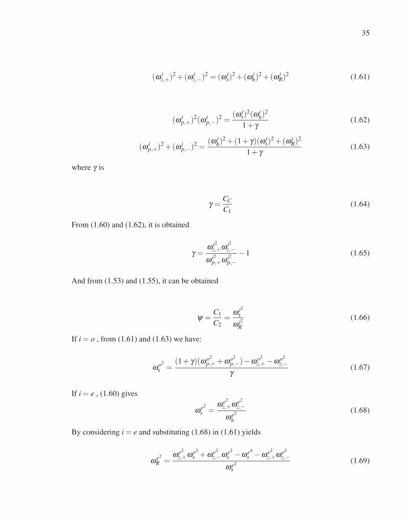
35
(ω iz,+)
2 +(ω iz,−)
2 = (ω is)
2 +(ω ih)
2 +(ω iR)
2 (1.61)
(ω ip,+)
2(ω ip,−)
2 =(ω i
s)2(ω i
h)2
1+ γ(1.62)
(ω ip,+)
2 +(ω ip,−)
2 =(ω i
h)2 +(1+ γ)(ω i
s)2 +(ω i
R)2
1+ γ(1.63)
where γ is
γ =CC
C1(1.64)
From (1.60) and (1.62), it is obtained
γ =ω i2
z,+ω i2z,−
ω i2p,+ω i2
p,−−1 (1.65)
And from (1.53) and (1.55), it can be obtained
ψ =C1
C2=
ω i2s
ω i2R
(1.66)
If i = o , from (1.61) and (1.63) we have:
ωo2
s =(1+ γ)(ωo2
p,++ωo2
p,−)−ωo2
z,+−ωo2
z,−γ
(1.67)
If i = e , (1.60) gives
ωe2
s =ωe2
z,+ωe2
z,−ωe2
h
(1.68)
By considering i = e and substituting (1.68) in (1.61) yields
ωe2
R =ωe2
z,+ωe2
s +ωe2
z,−ωe2
s −ωe4
s −ωe2
z,+ωe2
z,−ωe2
s(1.69)

36
Substituting (1.69) in (1.66) yields
(1+ψ)(ωes )
4 −ψ((
ωez,+
)2+(ωe
z,−)2)(ωe
s )2 +ψ
(ωe
z,−ωez,+
)2= 0 (1.70)
the formulas (1.53) to (1.55) are rewritten when i = e and i = o as follows
ωos = 2π f o
s =1√
C2(L2 −Lm2)ωe
s = 2π f es =
1√C2(L2 +Lm2)
(1.71)
ωoh = 2π f o
h =1√
C1(L1 −Lm1)ωe
h = 2π f eh =
1√C1(L1 +Lm1)
(1.72)
ωoR = 2π f o
R =1√
C1(L2 −Lm2)ωe
R = 2π f eR =
1√C1(L2 +Lm2)
(1.73)
From (1.72), L1 and Lm1 can be derived as follows
L1 =1
2C1
[1
ωeh
2+
1
ωoh
2
](1.74)
Lm1 =1
2C1
[1
ωeh
2− 1
ωoh
2
](1.75)
Similarly, L2 and Lm2 can be obtained from (1.71)
L2 =1
2C2
[1
ωes2+
1
ωos
2
](1.76)
Lm2 =1
2C2
[1
ωes2− 1
ωos
2
](1.77)
Since, the network parameters are positive, by considering (1.75), the below term should be
satisfiedf os
f es<
f oz,+ f o
z,−f ez,+ f e
z,−(1.78)

CHAPTER 2
DIRECT SYNTHESIS OF LUMPED-ELEMENT SINGLE- AND DUAL- NARROWBANDPASS FILTERS IN LTCC
Aref Pourzadi1, Mohsen Niayesh1, Ammar Kouki1
1 Département de Génie Électrique, École de Technologie Supérieure,
1100 Notre-Dame Ouest, Montréal, Québec, Canada H3C 1K3
Manuscript submitted to IEEE Transactions on Circuits and Systems I: Regular Papers in
November 2019.
Abstract
In this paper, the design of a new compact second-order lumped-element narrow bandpass fil-
ter (SNBPF) with a narrow 10 dB fractional bandwidth (FBW) (less than 3%) is presented.
Using even and odd mode analyses, the working mechanism of the SNBPF circuit model is
explained and an analytical design procedure is provided to obtain the element values. To re-
ject spurious signals, two transmission zeros (TZs) are generated in both sides of the center
frequency. Manipulating SNBPF circuit model, a single narrow frequency response is gener-
alized to dual-narrowband frequency responses (DNBPF). Performing the same analysis, the
working mechanism and design procedure of the DNBPF topology are fully described. To
demonstrate the theory of both narrow bandpass filters (NBPFs), two design examples are
provided. To reach a very compact size and enough flexibility to build inductive couplings,
physical layouts are realized in the form of 3-D configuration using low-temperature cofired
ceramic (LTCC) technology.
Introduction
Narrowband standards such as the global positioning system (GPS)Liu et al. (2010), per-
sonal communication services (PCS)Kim et al. (1999) and wireless communication services
(WCS)Chetouah et al. (2016) are commonly referred with respect to the industrial applications

38
of the single narrow bandpass filters (SNBPFs). These filters would allow narrow-bandwidth
modulated signals to be extracted from multiple interfering signals and improve system sig-
nal to noise ratio (SNR). Over the past few years, several classes of narrow bandpass fil-
ters have been developed with various features. Typical reported strategies for the SNBPFs
realizations include the following: substrate integrated waveguides (SIW)He et al. (2014),
cavity resonatorsLorente et al. (2013), parallel coupled lines, split ring resonators and high-
temperature superconductors (HTS) using planar microstrip technology Shao & Lin (2015);
Liu et al. (2016); Li et al. (2006), active SNBPFs implemented in CMOSSu & Tzuang (2012)
and realized lumped-element structures in LTCC Brzezina et al. (2009); Xu et al. (2016b).
The properties of existing reported strategies have been summarized, as shown in table 2.1.
Utilization of active SNBPFs is limited due to the power consumption. SIWs and filters us-
ing microstrip technology have a relatively bulkier size at low frequencies, which limits their
integration with other blocks. Lumped-element topologies are highly recommended for filters
operating at less than 5GHz in order to reach a very compact size.
Table 2.1 Properties OF The Proposed SNBPFs Design Strategies
SizeEasy
Integration SelectivityPower
Consumption Loss
SIW bulky yes medium no medium
Lumped-element compact yes medium no medium
Waveguide bulky poor high no low
HTS medium yes high no low
Microstrip medium yes medium no medium
Cmos compact yes medium yes low
Among various options for realizing lumped-elements, monolithic microwave integrated cir-
cuits (MMIC), surface mount devices (SMD) and LTCC, the last is more attractive. The 3-D
layout realization in LTCC provides a very compact size, apart from other features such as low
loss at high frequencies, integration capabilities in 3-D environment and low cost.

39
In the literature, several design methods of LTCC bandpass filters (BPFs) have been reported
with various degrees of performance and FWB. In Choi et al. (2003), using half-wavelength
coupled resonators leads to a bulky size for a designed circuit at microwave frequencies. In
Deng et al. (2005) and Yang et al. (2010), the limited number of TZs degrade due to band
rejection. In Xu et al. (2016b), the passband frequency responses are obtained based on a
direct synthesis method, but the very narrow FBW is not supported by the proposed circuit. In
Zhang et al. (2014) and Dai et al. (2014), the desired frequency responses cannot be precisely
specified, due to the proposed optimization design methodologies.
In this paper, a new topology of a lumped-element LTCC bandpass filter for applications with
small FBW is introduced. Existing three coupled inductors in the input of proposed circuit
model lead to an increase in the loaded Q-factor of the circuit at the given resonant frequency
which concludes narrowband frequency responses. Through an even/odd modes analysis, the
proposed SNBPF is supported by a straightforward design procedure that uses closed-form
synthesis equations to control even/odd mode poles. This analytical solution provides flexi-
bility, allowing the application of the new topology in different frequencies of spectrum and,
therefore, creates a narrow bandpass response of the network. To reject out-of-band spurious
signals, two TZs are appointed in both sides of the passband.
Further, it is demonstrated that the single bandpass is generalized to dual-band frequency re-
sponses through manipulation of the proposed SNBPF circuit model. In the light of increasing
demand for multiband wireless communication systems, some researches have been conducted
on LTCC filters with dual-band frequency responses, (see Lin et al. (2014); Xu et al. (2013);
Oshima et al. (2010); Chen et al. (2009); Chen (2005); Pourzadi et al. (2019)). Similar to
the SNBPF, a direct synthesis method with closed-form equations is provided to synthesize a
dual-narrow bandpass filter (DNBPF). In the new DNBPF, existing independent poles are asset,
for they have independent and controllable external quality factors at both bands. The center
frequencies can be adjusted, whereas wide or tight frequency separation between passbands is
possible.

40
Figure 2.1 (a) Circuit model of the proposed SNBPF. (b) Circuit model of the SNBPF
under even mode excitation. (c) Circuit model of the SNBPF under odd mode excitation

41
2.1 Design of LTCC SNBPF
2.1.1 Circuit Model of SNBPF
Fig.2.1(a) shows the circuit model of the SNBPF, which contains four major parts, namely,
input inductance [Lp], shunt resonator [C1,L1], series resonator [C2,L2] and input inductive
couplings [Lm1,Lm2]. Due to the symmetry of the circuit model, even and odd mode analysis
can be used. Under even/odd modes excitations, Fig.2.1(a) is decomposed into Fig.2.1(b) and
Fig.2.1(c), respectively. The input impedance of the equivalent circuit under even excitation is
calculated as follows:
Zine =jω
[(Lm2
1 −L1Lp)C1ω2 +2Lp]
2−ω2C1L1(2.1)
The Zine resonates when 2−ω2C1L1 = 0. Equating DEN (Zine) to zero gives two poles out of
which only the positive pole is considered. This pole f pe is equated as shown in (2.2).
f pe =
1
2π
√2
C1L1(2.2)
The terms p and e indicate pole and even mode. Similar to the above analysis, under odd
excitation, the input impedance of the equivalent circuit can be obtained by (2.3).
Zino = jωLp − j2ωC2( jωLm2)2
1−2ω2C2L2− jωLm2
1
L1(2.3)
Repeatedly, Zino resonates when DEN (Zino) is equal to zero. Equating 2−ω2C2L2 = 0 gives
two poles out of which the positive one is of interest. The pole f po is found to be as follows:

42
f po =
1
2π1√
2C2L2
(2.4)
The term o indicates odd mode. f pe and f p
o determine the nature of the frequency, response
of the circuit of Fig.2.1a. Fig.2.2 illustrates a typical example for even/odd impedance curves
versus frequency to show how the placements of the poles create a narrow bandpass frequency
response.
0.5 1 1.5 2 2.5 3 3.5 4−40
−20
0
20
40
60
80
100
Frequency(GHz)
|Ze|&
|Zo|(d
B)
fe p
fo p
Zo
Ze
Figure 2.2 Input impedances of even and odd modes
2.1.2 Design Procedure of SNBPF
A second-order Chebyshev bandpass frequency response Dancila & Huynen (2011) is applied
to calculate the two poles, f pe and f p
o . We start with the assigned center frequency fc, the
desired bandwidth BW and the in-band return loss RL. The values of the coupling coefficient
KM and the external quality factor Qe correspond to the BW , fc and gi elements by the following
equations Dancila & Huynen (2011):

43
KM =BWfc
√1
g1g2(2.5)
and
Qe =g0g1 fc
BW(2.6)
fc can be calculated by averaging the pole frequencies, as
fc =f pe + f p
o
2(2.7)
and KM corresponds to f pe and f p
o by formula Hong & Lancaster (2004):
KM =( f p
e )2 − ( f p
o )2
( f pe )2 +( f p
o )2(2.8)
Using a nonlinear optimization technique for solving (2.7) and (2.8), one obtains optimal values
of f pe and f p
o . In equations (2.2) and (2.4), the arbitrary values of C1 and C2 constitutes degrees
of freedom in our design procedure and, then, are used to calculate of L1 and L2. Noting that the
values of C1, C2, L1 and L2 must be adjusted according to fabrication restrictions. To calculate
the values of the remained parameters Lm1, Lm2 and Lp, we continue with the the frequency
responses of the proposed SNBPF which are given by:
S11 = S22 =ZineZino −Z2
0
(Zine +Z0)+(Zino +Z0)(2.9)

44
S12 = S21 =Z0(Zine −Zino)
(Zine +Z0)+(Zino +Z0)(2.10)
where Z0 = 50 is the port impedance. Solving S12 = S21 = 0 proves existence of two TZs,
which are excited by the following equation:
C1C2L21Lm2
2ω4−2C2(L1Lm2
2 +L2Lm21)ω
2 +Lm21 = 0
(2.11)
in the frequencies of
ω1Z =
√√√√−b+√
b2 −4C1C2(L1Lm2Lm1)2
2C1C2L21Lm2
2
(2.12)
ω2Z =
√√√√−b−√
b2 −4C1C2(L1Lm2Lm1)2
2C1C2L21Lm2
2
(2.13)
where b =−C2(L1Lm22+L2Lm2
1), ω1Z = 2π f1Z and ω2Z = 2π f2Z . f1z and f2z are corresponded
to fc as
f1z =2 fc − γ
2(2.14)
f2z =2 fc + γ
2(2.15)
where γ indicates the value of frequency spacing between TZs, f1z and f2z . From (2.14)
and (2.15), the values of f1z and f2z are calculated by inserting the assigned value of γ and

45
then solving (2.12) and (2.13), we can find the values of Lm1 and Lm2. With the obtained
element values and using the given Qe for the desired passband, we can compute Lp. Qe can
be approximated by the following equationXu et al. (2016a):
Qe ≈π[
f pe τS11( f p
e )+ f po τS11( f p
o )]
2(2.16)
where
τS11( f pe ) =−∂φS11( f p
e )
2π∂ f(2.17)
and
τS11( f po ) =−∂φS11( f p
o )
2π∂ f(2.18)
where τS11( f pe ) and τS11( f p
o ) are the group delays of S11 at the frequencies of f pe and f p
o ,
respectively. Using a graphical solution, we sweep Lp to find a suitable value for satisfying the
required Qe. The above-detailed synthesis steps of SNBPF design are summarized in Fig.2.3,
in the form of a chart.
2.1.3 Simulation and Experimental Results of SNBPF
Using the above synthesis procedure, this section illustrates the design and prototyping of a
second-order Chebysheve WCS narrow bandpass filter operating at 2.2925-2.3325 GHz. Based
on the desired frequency band, we have fc = 2.3125 GHz and BW = 40 MHz. By requiring a
return loss of 20 dB at Passband, the filter’s gi are found to be g0 = 1, g1 = 0.6923, g2 = 0.5585
and g3 = 1.2396. Using the values of gi elements, fc and BW , in (2.5) and (2.6), we obtain
KM = 2.78% and Qe =40. Then, (2.7) and (2.8) are used in a nonlinear optimization algorithm
in MATLAB to calculate the values of the pole frequencies, which are found to be f pe = 2.345
GHz and f po = 2.28 GHz. As the degrees of freedom, the values of C1 and C2 are selected to

46
Figure 2.3 Flowchart of synthesis steps for the proposed SNBPF design
be 1.6 pF and 1.9 pF, and from (2.2) and (2.4), the values of L1 and L2 are calculated to be
5.76 nH and 1.28 nH, respectively. The fabrication process and it’s limitations should be taken

47
to account for the values of these elements. In addition, high self resonance frequency (SRF)
and high quality factorMousavi & Kouki (2015) should be considered for the targeted design.
Selecting γ to be 520 MHz and using (2.14) and (2.15), we compute f1z = 2050 MHz and f1z =
2570 MHz, which are then used in (2.12) and (2.13) to calculate the values of Lm1 and Lm2.
Solving (2.12) and (2.13), Lm1 and Lm2 are found to be 0.793 nH and 0.379 nH, respectively.
The remaining parameter Lp is computed through the graphical solution. As shown in Fig.2.4,
Lp is swept from 0.1 to 5 nH and Qe is calculated using (2.16). It can be realized that the ideal
value of Lp is 2.5 nH to meet the given Qe=40. Fig.2.5 plots the obtained frequency responses
of the designed SNBPF circuit model. Using the 3-D field simulator HFSS, the calculated
values of the lumped-elements are synthesized following the technique presented in Brzezina
et al. (2009) and then integrated to form the entire filter on LTCC. Regarding the required
capacitance and inductance values, we choose to implement capacitors based on multilayer
parallel plates and inductors using curved line configurations. An optimization of the overall
dimensions are performed to obtain the final physical layout, as shown in Fig.2.6. The SNBPF
is fabricated on LTCC Ferro A6M, with the dielectric constant of 5.7, and the loss tangent of
0.001. The LTCC wafer is consists of seven ceramic sheets, two sheets with the thickness of
2 mil and five sheets with the thickness of 5 mil, along with three metal layers. The material
of the conductors is silver with a thickness of 0.008 mm and the diameter of vias is 0.137 mm.
The top view of the fabricated circuit is shown in Fig.2.7. The final dimensions of the fired
filter are 6.2 mm× 4.14 mm with the total fired thickness of 0.736 mm. As shown in Fig.2.8,
there is a good agreement between EM simulation and the measurement results. The insertion
loss is about 2 dB and the return loss is greater than 18 dB. The two TZs appear at both sides of
the passband and are located at 2 GHz and 2.71 GHz frequencies. Finally, Table 2.2 includes
the comparison performances of bandpass LTCC filters with various FWBs.

48
0 0.5 1 1.5 2 2.5 3 3.5 426
28
30
32
34
36
38
40
42
Lp (nH)
Qe Lm2=0.5nH
Lm2=0.45nH
Lm2=0.379nH
Figure 2.4 Variation of Lp versus Qe
0.5 1 1.5 2 2.5 3 3.5 4−80
−70
−60
−50
−40
−30
−20
−10
0
Frequency(GHz)
|S11
|&|S
12|(d
B)
S12
S11
Figure 2.5 Theoretical and simulation results of the proposed SNBPF circuit model

49
Figure 2.6 3-D view of proposed NBPF. The dimensions are determined as follows (in
millimeters):L1 = 0.35, L2 = 0.6, L3 = 0.2, L4 = 1.09, L5 = 0.9, L6 = 0.75, L7 = 0.4, L8 =
1.55, L9 = 0.35, L10 = 0.4, L11 = 1.5, L12 = 3.74, L13 = 1, L14 = 0.74, L15 = 0.5, L16 =
0.73, L17 = 1, L18 = 2.3, L19 = 1
2.2 Design OF LTCC DNBPF
2.2.1 Circuit Model of DNBPF
The single narrow bandpass frequency response is generalized to the dual-band frequency re-
sponse through a small manipulation in the topology of the proposed SNBPF. Schematic of

50
Figure 2.7 Photograph of fabricated SNBPF
0.5 1 1.5 2 2.5 3 3.5 4−50
−40
−30
−20
−10
0
Frequnecy(GHz)
|S11
|&|S
12|(d
B)
HFSS
Measurment
S12
S11
Figure 2.8 EM simulated and measured frequency responses of SNBPF
DNBPF is introduced by replacing the series capacitors C2 of Fig.2.1(a) by a shunt grounded
form. Fig.2.9(a) shows the circuit model of the DNBPF. Similar to previous designs, we use the
even/odd mode excitations for analysis and working mechanism investigations. The even/odd
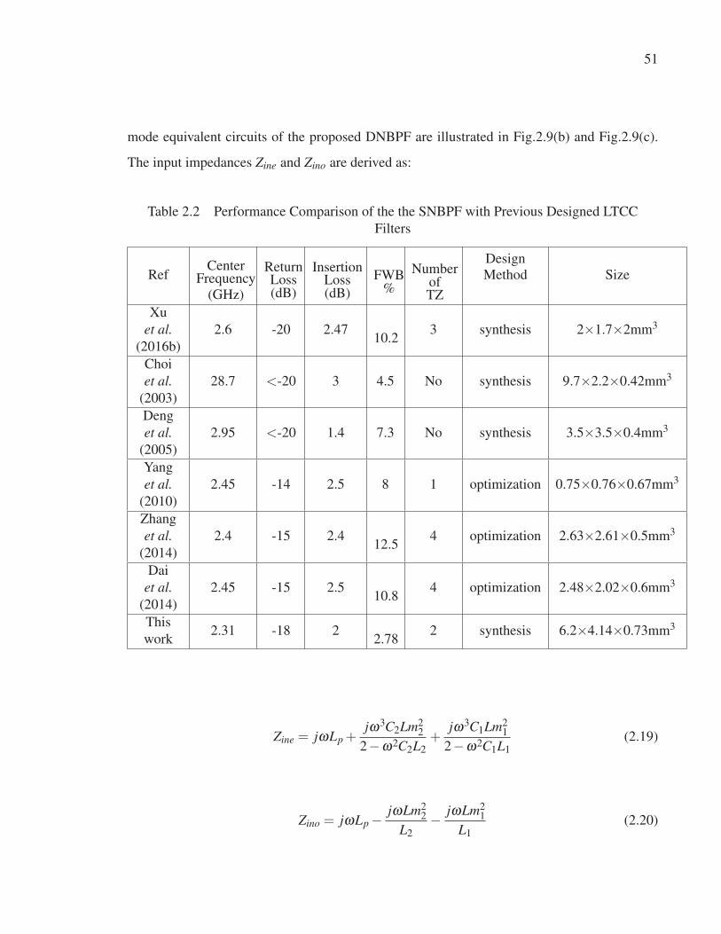
51
mode equivalent circuits of the proposed DNBPF are illustrated in Fig.2.9(b) and Fig.2.9(c).
The input impedances Zine and Zino are derived as:
Table 2.2 Performance Comparison of the the SNBPF with Previous Designed LTCC
Filters
RefCenter
Frequency(GHz)
ReturnLoss(dB)
InsertionLoss(dB)
FWB%
NumberofTZ
DesignMethod Size
Xu
et al.(2016b)
2.6 -20 2.4710.2
3 synthesis 2×1.7×2mm3
Choi
et al.(2003)
28.7 <-20 3 4.5 No synthesis 9.7×2.2×0.42mm3
Deng
et al.(2005)
2.95 <-20 1.4 7.3 No synthesis 3.5×3.5×0.4mm3
Yang
et al.(2010)
2.45 -14 2.5 8 1 optimization 0.75×0.76×0.67mm3
Zhang
et al.(2014)
2.4 -15 2.412.5
4 optimization 2.63×2.61×0.5mm3
Dai
et al.(2014)
2.45 -15 2.510.8
4 optimization 2.48×2.02×0.6mm3
This
work2.31 -18 2
2.782 synthesis 6.2×4.14×0.73mm3
Zine = jωLp +jω3C2Lm2
2
2−ω2C2L2+
jω3C1Lm21
2−ω2C1L1(2.19)
Zino = jωLp − jωLm22
L2− jωLm2
1
L1(2.20)

52
Zine will resonate when 2−ω2C2L2 = 0 and 2−ω2C1L1 = 0 . Therefore, the proposed NDBPF
has four poles which only positives are desired. These poles are determined by
f p1e =
1
2π
√2
C1L1(2.21)
f p2e =
1
2π
√2
C2L2(2.22)
Equating S12 =0 in (2.8) proves that the DNBPF generates one TZ located at given frequency
fz =1
2π
√2(L1Lm2
2 +L2Lm21)
C1L21Lm2
2 +C2L22Lm2
1
(2.23)
2.2.2 Design Procedure of DNBPF
Center frequency of first passband f1c, and of second passband f2c, the external quality factor
of first passband Q1e, and of second passband Q2e and transmission zero fz are assigned as the
design specifications of the DNBPF. As degrees of freedom, we select proper values for C1 and
C2, and then using the given center frequencies and equations (2.21) and (2.22), the values of
L1 and L2 are obtained. It should be noted that f1c and f2c are approximated as f1c≈ f p1e and
f2c≈ f p2e in (2.21) and (2.22). The shape and selectivity of the two passbands are controlled by
the values of Q1e and Q2e, which are calculated from Hong & Lancaster (2004).
Q1e =f1C
Δ f 3dB1C
= π f1CτS11( f1C) (2.24)
Q1e =f2C
Δ f 3dB2C
= π f2CτS11( f2C) (2.25)

53
Figure 2.9 (a) Circuit model of the proposed DNBPF. (b) Circuit model of DNBPF
under even mode excitation. (c) Circuit model of DNBPF under odd mode excitation

54
where τS11( f1C) and τS11( f2C) are the group delays of S11 at the center frequencies. The re-
maining unknown values Lp , Lm1 and Lm2 are calculated by solving the system equation in-
cluding (2.23) to (2.25). One solution to solve this system equation is to use specific nonlinear
programming solver FMINCON in MATLAB. FMINCON find the minimum of error function
by fitting different values Lp , Lm1 and Lm2 in (2.23) to (2.25). The total error function is
defined as
min(eT ) = e1 + e2 + e3 (2.26)
where
e1 = |given(Q1e)− calculated(Q1e)| (2.27)
and
e2 = |given(Q2e)− calculated(Q2e)| (2.28)
and
e3 = |given(Q3e)− calculated(Q3e)| (2.29)
Note that due to approximations f1c≈ f p1e and f2c≈ f p
2e in the proposed design procedure, a
central slight shifting is expected in the center frequencies. With small tuning of C1 and C2
values, both bands can be adjusted at the desired frequencies, but the nonlinear solving process
is affected by the new values of C1 and C2. Furthermore, one has to recalculate Lp, Lm1 and
Lm2 using updated C1 and C2 to meet the given values of Q1e and Q2e. The synthesis steps of
the DNBPF design procedure are summarized in Fig.2.10, in the form of a chart.
2.2.3 Simulation and Experimental Results of DNBPF
This section illustrates a designed and prototyped of DNBPF operating at PCS(1.905-1.910)
GHz / WCS(2.305-2.320) GHz to validate the theory explained in the previous section. Based
on the desired frequencies and the given external quality factors, we have f1c = 1.9075 GHz,
f2c = 2.3125 GHz, Q1e = 18, Q2e = 22 and TZ is assigned to be 2.1 GHz. To follow the design
procedure, we need to select the values of C1 and C2. Selecting C1 = 2.6 pF and C2 = 4.7 pF and
using (2.21) and (2.22), then L1 and L2 are calculated to be 5.36 nH and 2.02 nH. By solving the

55
Figure 2.10 Flowchart of synthesis steps for DNBPF design
system equation including (2.23) to (2.25) in MATLAB, the remaining parameters are obtained
Lp = 2.96 nH, Lm1 = 1.121 nH and Lm2 = 0.562 nH. With the obtained element values, we can
compute the frequency responses using (2.9) and (2.10). Dashed lines in Fig.2.11 illustrate the
frequency response of the DNBPF circuit model. As can be seen, there is a slight shifting at
center frequencies and they are not displayed as expected. These are due to the approximations
f1c≈ f p1e and f2c≈ f p
2e and can be easily corrected with a slight tuning of the element values
C1= 2.67 pF and C2= 4.81 pF. The values of Lp, Lm1 and Lm2 need to be recalculated to
meet the given external quality factors due to updated capacitors. The frequency responses are
computed with the updated element values: C1= 2.67 pF, C2= 4.81 pF, L1= 5.36 nH, L2= 2.02
nH, Lp= 2.564 nH, Lm1= 1.32 nH and Lm2= 0.613 nH, as shown in solid lines in Fig.2.11.

56
1 1.5 2 2.5 3 3.5 4−80
−70
−60
−50
−40
−30
−20
−10
0
Frequency(GHz)
|S11
|&|S
12|(d
B)
S12
S11
Dashed Lines: untuned values of C1 and C
2Solid Lines: tuned values of C
1 and C
2
Figure 2.11 Simulated frequency responses of DNBPF circuit model
Table 2.3 Performance Comparison of the DNBPF with Previous Designed dual-band
LTCC Filters
Reference
CenterFrequency
(GHz)
f1c/ f2c
ReturnLoss(dB)
RL1/RL2
InsertionLoss(dB)
IL1/IL2
FWB1/FWB2
%Numberof TZ
Design
Method Size
Lin et al.(2014)
2.45/5.25 -12/-16.8 2/2.3 12.2/5.7 2 synthesis 2mm × 1.25mm × 0.9mm
Xu et al.(2013)
59.78/61.56 -15/-15 3.6/3.55 2.1/2.2 2 synthesis ——–
Oshima
et al. (2010)3.96/7.92 <-12 2.5 40/40 3 synthesis 7.5mm × 3.8mm × 0.386mm
Chen et al.(2009)
30.3/39.3 -17 4.8 6/6 4 synthesis 4.12mm × 3.92mm × 0.832mm
Chen
(2005)2.4 2.47/5.22 3.15/3.9 8.1/5.7 2 synthesis 2.69mm × 1.77mm × 0.13mm
Pourzadi
et al. (2019)0.915/2.45 -18/-22 2/1.5 5.46/5.71 4 synthesis 7.2mm × 6.88mm × 0.56mm
This work 1.9075/2.3125 <-17 1.8 0.26/0.64 1 synthesis 9.3mm × 4.16mm × 0.736mm
Fig.2.12 illustrates a 3-D view of the simulated DNBPF in the HFSS. The thicknesses and
numbers of LTCC sheets are the same as those we have used for the design of SNBPF. Fig.2.13
shows the photograph of the fabricated circuit. The final dimensions of the fired filter are 9.3
mm × 4.16 mm × 0.736 mm. The results of the EM simulations and the measurements, are
depicted in Fig.2.14. The dashed and solid lines demonstrate the frequency responses of the
EM simulations and measurements respectively. The measured insertion losses are around 1.8

57
dB and the return losses are better than 17dB at both bands. Finally, the measurements show
that the transmission zero is located at 2.12 GHz. Finally, in Table 2.3, the performances of
several designed dual-band LTCC filters are compared.
Figure 2.12 3-D view of proposed DNBPF. The dimensions are determined as follows
(in millimeter):L1 = 1.55, L2 = 1, L3 = 0.8, L4 = 0.6, L5 = 1, L6 = 1, L7 = 3, L8 = 1, L9 =
1, L10 = 0.5, L11 = 3.14, L12 = 0.4, L13 = 1.25, L14 = 0.5, L15 = 1.44, L16 = 0.9
Conclusion
In this paper, direct synthesis of new single- and dual-band bandpass filters with small FWBs
was presented. Using even and odd modes analysis, the nature of frequency responses and the
working mechanisms for both topologies were explained. The design procedures used closed-

58
Figure 2.13 Photograph of fabricated DNBPF
0.5 1 1.5 2 2.5 3 3.5 4−50
−40
−30
−20
−10
0
Frequency(GHz)
|S11
|&|S
12|(d
B)
Measurment
HFSS
S12
S11
Figure 2.14 EM simulated and measured frequency responses of DNBPF
form equations to calculate the values of network elements for the given center frequencies
and bandwidth. The proposed filter topologies and synthesis techniques were applied to the
design of an SNBPF and a DNBPF using LTCC technology. The prototypes of these filters

59
were successfully simulated and measured with excellent agreement between the simulation
results and the measurement results.


CHAPTER 3
A FAST TECHNIQUE FOR REALIZATION OF LUMPED-ELEMENTS VALUESINTO 3D PHYSICAL LAYOUT ON LTCC
Aref Pourzadi1, Arash Adibi1, Ammar Kouki1
1 Département de Génie Électrique, École de Technologie Supérieure,
1100 Notre-Dame Ouest, Montréal, Québec, Canada H3C 1K3
Manuscript submitted to IEEE Transactions on Components, Packaging and Manufacturing
Technology in November 2019.
Abstract
We propose a methodology for the fast translation of ideal lumped-element values to the form
of a 3D physical layout using low-temperature co-fired ceramic (LTCC) dielectric. we explain
how this approach is implemented without requiring complex formulas and use a simulation-
based process which leads to consume less optimization/tuning processing time. The proposed
methodology is applied to the design of a dual-band bandpass filter (D-BPF) operating at cen-
ter frequencies 2.4 GHz, and 5.2 GHz and its layout is realized in the form of 3D physical
layout. The two commercial simulators, advanced design systems (ADS) and high-frequency
structure simulator (HFSS), are used to simulate ideal lumped-element schematics and perform
electromagnetic (EM) simulations on the LTCC layout, respectively.
Introduction
In radio frequency engineering, the physical realization of microwave devices are selected
based on features such as operating frequency, size, cost, bandwidth, and loss. Circuits such
as filter, couplers, and baluns, can be structured according to one of three commonly used
approaches, including distributed transmission lines Zhu & Abbosh (2016); Pourzadi et al.
(2012), cavities Zhou et al. (2018); Shen et al. (2013), and lumped-elements Tang (2007); Feng
et al. (2017). The major drawback of transmission lines and cavities is their bulkiness at lower

62
frequencies, which creates difficulties in size reduction and integration. Lumped-elements are
recommended especially when they are realized in a 3D configuration of low-temperature co-
fired ceramics (LTCC) technology. This technology offers a good platform for designing very
compact sized devices and multichip modules (McM).
As reported in the literature, many successful lumped-element designs Shafique & Robertson
(2011); Shen et al. (2009); Mousavi & Kouki (2015); Brzezina et al. (2009); Brzezina & Roy
(2014); Zheng & Sheng (2017); Zhou et al. (2016); Lee et al. (2012); Brzezina & Roy (2014)
have been fabricated in LTCC. In these references, ideal schematics are analyzed, working
mechanisms investigated and then element values are transformed into the physical layouts us-
ing an electromagnetic (EM) solver. In the conventional methodology for physical realization,
each lumped-element, is designed individually in an EM simulator software. The designed
physical elements are combined to form the entire 3D LTCC layout of the proposed circuit,
and then the overall dimensions are optimized to obtain the expected frequency responses in
the EM simulator. In Brzezina et al. (2009), an improved methodology was introduced, which
is a hybrid of 3D physical and ideal circuit elements. Hybrid technique is more time-efficient
than conventional approach but still includes guesswork in parametric tuning steps. Depending
on circuit complexity, the number of elements and operating frequency, tuning steps in both
implementation strategies (conventional and hybrid) can be very time-consuming, due to com-
pensation of parasitic effects and mutual coupling between elements. In fact, parasitic effects
and mutual couplings can change the inductance and capacitance values of elements, or in the
worst case scenario, they can add redundant elements to the proposed ideal model. Also, exist-
ing elements with dependent values to each other in the schematic, such as coupled inductors,
generate more implementation difficulties Brzezina & Roy (2014).
In this paper, we present a direct methodology by using a correlation strategy between HFSS
and ADS simulator softwares. In this technique, the processing time of physical realization is
reduced significantly due to the elimination of dimension tuning the steps. This facilitates a bet-
ter understanding of the existing parasitic effects and provides less efforts to obtain the desired
experimental results that are much closer to the ideal model. The usefulness of the proposed

63
technique is demonstrated through a practical design example, which is a recently published
schematic of a lumped-element Dual-Band bandpass filter (D-BPF) Pourzadi et al. (2019). To
prove the validity of this technique, a physical prototype operating at center frequencies 2.4-5.2
GHz is fabricated in LTCC.
This remainder of the paper is be organized as follows: section 1 describes details of the
proposed technique. In, section 2, a design study is defined and the implementation steps
related to transforming element values to physical layout are explained using HFSS and ADS
simulators. The final simulation and fabrication results are presented in section 3. Concluding
remarks are given in section 4.
3.1 Proposed Physical Realization Methodology of Lumped-Elements In LTCC
Fig.3.1 compares the three realization methodologies of LTCC physical layouts in the form of
charts, including (a) conventional approach, (b) hybrid methodology and (c) the proposed strat-
egy in this paper, the correlation between HFSS and ADS. As shown in Fig. 3.1, the highlighted
steps, the simulation of the ideal schematic and the design of each lumped-element individu-
ally are common in the three techniques. In the conventional approach, each lumped-element
is designed in an EM simulator and sized based on the given inductance or capacitance values,
the high Q-factor and the self-resonance frequency (SRF). The designed physical elements are
integrated into one structure to form the complete 3D LTCC layout, and then EM simulations
are performed on the structure. The final LTCC layout needs time-consuming parametric tun-
ings on dimensions to obtain the desired results. This approach works for structures with a
small number of elements. For the hybrid method, the first two steps are similar to those of
the conventional approach. In the integrated layout, some of the physical elements are replaced
with ideal values and then the EM parametric tuning is performed on the hybrid layout to adjust
the dimension of the physical elements. Once the response is as expected, the ideal element
models are replaced with their physical prototypes and a second round of EM physical tuning
is performed on the entire 3D LTCC layout. Hybrid method reduces the overall time spent

64
optimizing rather than the conventional approach, but the increasing number of elements, (see
Mousavi & Kouki (2014)) still degrades the functionality of this method.
In our proposed methodology, tuning steps are eliminated. Hence, the time spent in the trans-
formation into physical layout and the efforts required to have a perfect response are both
reduced significantly. Also, it provides more convenience and flexibility with respect to imple-
mentation of lumped-elements with dependent values, such as coupled inductors. The parasitic
effects and mutual couplings are compensated during the simulation steps and accounted in the
final results. The outlined steps of the flowchart are explained as follows:
a. The ideal schematic, which we name as schematic I, is simulated in ADS and the S-
parameters simulation results are obtained.
b. Each lumped capacitor and inductor is modeled individually in the HFSS, and the varia-
tion curves of L, C and Q-factor versus frequency are obtained using equations 3.1 to 3.3
Brzezina et al. (2009).
L =Im(Z11)
ω(3.1)
C =Im(Y11)
ω(3.2)
Q =Im(Z11)
Re(Z11)(3.3)
The elements are sized physically to meet the given inductance or capacitance values at
the operating frequency while simultaneously providing the maximum value of the Q-
factor and a high SRF. High Q-factor is demanded in circuit design as it has a substantial
influence on the in-band insertion loss.
c. Interconnect the designed physical elements with their initial dimensions to form the en-
tire 3D LTCC layout in the HFSS. It is required to have a preliminary idea about number
of stack layers and the placement configuration of elements. With the completion of the
first round of EM simulation in the HFSS, as we had expected, there are dissimilarities
between the obtained EM and the ideal model (schematic I) S-parameters in the ADS.

65
Figure 3.1 Flow charts of three realization strategies including: (a) conventional
approach (b) hybrid methodology (c) proposed correlation strategy between HFSS and
ADS

66
d. This step entails finding the values of elements which are corresponded to the initial 3D
LTCC layout. Fig .3.2 illustrates the simulation procedures for this step in the ADS envi-
ronment. The obtained EM s-parameters S11 and S12 (in previous step) are imported into
the ADS in the form of an S2P file. The elements of the ideal model (schematic I) are
replaced with the variable elements and the new network is named schematic II. Then,
using Optim and Goal tools, the optimization process is set up. In the Optim window,
the type of optimizer and the number of iterations are selected. In the Goal window, we
define two expressions as final targets, which are |SEM11 − SII
11| and |SEM12 − SII
12|, and add
limit criteria 0 for both expressions to stop the solver. The superscripts EM and II indi-
cate imported EM and schematic II S-parameters, respectively. Running the optimization
solver, the optimizer computes element variables in each iteration to meet the limit crite-
ria of the defined expressions in the Goal windows. The optimizer compares the obtained
frequency responses of schematic II with the imported S2P file and then modifies the val-
ues of elements in next iteration to minimize the design goal errors. Note that assigning
reasonable concentrations on element values would reduce the convergence time of the
optimizer.
e. In the previous step, the values of schematic II were computed such that the frequency
responses of the network was matched perfectly with the EM frequency responses of the
initial 3D LTCC layout. In this step, the target is to modify the values of schematic II
elements and, consequently, the physical dimensions of elements of the initial 3D LTCC
layout to meet the frequency responses of schematic I. We proceed with this approach
with the following strategy. In the ADS environment, we select one of the elements of
schematic II and replace its value with the value of the same element from schematic I.
Then, s-parameter simulation is performed on the modified schematic II. Note that in the
modified network, the rest of elements are the same as we had computed in the step 4.
Next, in the HFSS, the dimensions of corresponding element are resized such that the
EM frequency responses follow the frequency responses of the modified schematic II.
Repeating the above mentioned details, all the remaining elements of modified schematic
II are replaced with the values of schematic I, in turn. Consequently the physical elements

67
Figure 3.2 Simulation procedures in step 4

68
of the 3D LTCC layout are resized, which leads to an excellent agreement between the
simulation results of layout and schematic I.
3.2 Circuit Realization Example
This section illustrates the application of the proposed methodology to the transformation of
an ideal circuit model of a dual-band bandpass filter (D-BPF), presented in reference Pourzadi
et al. (2019), into a 3D LTCC layout. Using the synthesis procedure of Pourzadi et al. (2019),
the element values of the circuit model are computed to design and create a prototype D-BPF
operating at center frequencies 2.45 GHz and 5.2 GHz. Following the steps outlined in the
previous section, we proceed to realize the element values into a physical layout in LTCC, as
follows.
a. Fig.3.3a shows the schematic (schematic I) of the D-BPF, which consists of 13 elements
with the computed values of Cc = 0.68 pF, Cz = 0.2 pF, C1 = 1.69 pF, C2 = 1 pF, L1 −Lm1 = 1.04 nH, L2−Lm2 = 1.5 nH, Lm1 = 0.02 nH, Lm2 = 0.29 nH. Fig. 3.3b illustrates
the simulated s-parameters of the Schematic I in the ADS.
b. Using HFSS, each of the elements are individually sized to meet given inductance or
capacitance at 2.4GHz frequency. At this point, we have no idea about the final configu-
ration of the D-BPF including number of dielectric sheets and placement of the elements
in the layout. Thus, simplest forms of realizations are selected to find initial physical di-
mensions. We chose to realize capacitors and inductors using multilayer parallel plates
and straight lines respectively. The elements are simulated using two sheets of LTCC
Ferro A6M dielectric, with the thickness of each 93.98 um, dielectric constant of 5.9 and
the loss tangent of 0.002. Figs. 3.4 shows the characteristic variations of the elements
versus frequency, simulated in the HFSS, and Table 3.1 lists the physical dimensions, the
Q-factor and the SRF values. It should be noted that the simulation characteristics of the
element Lm1 are not provided, due to its small value (0.02 nH) and are physically realized
by a single via.

69
c. We interconnect the elements designed in step 2 to form the entire D-BPF in the HFSS,
as shown in Fig.3.5. The filter is simulated using five layers of green tapes with an overall
thickness of 469.9 um, 8-um thick silver and silver-filled 136-um-diameter vias. First
round of EM simulation are performed on the layout and the S-parameters are obtained.
Solid lines in Fig. 3.6 illustrates the frequency responses of the proposed D-BPF layout,
with initial physical dimensions. Note that, the interconnections between elements which
are not included in the ideal schematic, generate parasitic effects and unwanted mutual
couplings. In addition to these negative impacts, the dielectric and conductor losses cause
disagreements between the frequency responses of the final LTCC layout and the ideal
circuit model.
Table 3.1 List of designed elements and their characteristics.
ElementL1 −Lm1
= 1.04 nH
L2 −Lm2
= 1.5 nHLm2
= 0.29 nHC1
= 1.69 pF
C2
= 1 pFCz
= 0.2 pFCc
= 0.68 pF
SRF(GHz)
13.4 9.33 51 6.61 8.64 44.61 10.68
Q-Factor 106 102 97 50 55 63.7 58
Dimension(mm)
lL1 = 2.6 lL2 = 3.7lLm2 =0.75
lC1 = 1.4 lC2 = 1.1 lCz = 0.5 lCc = 0.9
WL = 0.2 WL = 0.2 WL = 0.2WC1 =
1.4WC2 =
1.1WCz =
0.5WCc =
0.9
Table 3.2 Comparison table of Schematic I and Schematic II element values.
ElementsL1 −Lm1
(nH)L2 −Lm2
(nH)
Lm2
(nH)Lm1
(nH)C1
(pF)C2
(pF)Cz
(pF)Cc
(pF)
Schematic I1.04 1.5 0.29 0.02 1.69 1 0.2 0.68
Schematic II0.63 1.87 0.41 0.038 4.15 0.94 0.39 1.06

70
Figure 3.3 a) Schematic I Pourzadi et al. (2019) b) Simulated frequency responses of
Schematic I in ADS
d. Performing EM simulation on the initial D-BPF layout in the HFSS, the obtained s-
parameters SEM11 and SEM
12 are extracted in the form of touchstone file. Then, we select
two port s-parameter item in the ADS and import the touchstone data. Next, in the ADS

71
Figure 3.4 Simulated characteristics of elements in the HFSS a) simulated inductances
of L1, L2 and Lm2 versus frequency b) simulated Q-factors of L1, L2 and Lm2 versus
frequency c) simulated capacitances of C1, C2, Cz and Cc versus frequency d) simulated
Q-factors of C1, C2, Cz and Cc versus frequency e) top view and 3D view of straight line
inductor f) top view and 3D view of parallel plate capacitor

72
Figure 3.5 3D and top views of structured initial EM circuit in HFSS. Dimensions are in
millimeters, L1=1.4, L2=1.1, L3=1.1, L4=2.3, L5=0.9, L6=1.5, L7=0.5, L8=0.5, L9=0.9,
L10=1.4, L11=1.1, L12=1.4, L13=1.1, L14=0.75, L15=1.3, width of lines=0.2

73
Figure 3.6 Simulated frequency responses, solid line: initial EM circuit and Dashed
line: Schematic II
environment we set up the optimization controller, select type of optimizer to gradient
with maximum 6000 iterations, and define goal expressions |SEM11 −SII
11| and |SEM12 −SII
12|.The optimizer starts calculation process of Schematic II elements and provides an error
criterion in the form of number for estimation of differences between the computed fre-
quency responses of Schematic II and touchstone file. In this D-BPF layout realization,
the optimization process is converged to the minimum value of error number 25 after 6000
iterations. Fig.3.6 shows an excellent agreement between the S-parameters of Schematic
II and D-BPF LTCC layout which demonstrates the Schematic II is an accurate circuit
model for the initial layout. Table 3.2 lists the element values of Schematic I and II.
It should be mentioned that due to existing mutual couplings, loss effects and intercon-
nections, the optimizer cannot provide error number close to 0 but convergence to small
values guarantees good agreement between the final results.

74
e. In this step, the target is to modify the dimensions of the elements of D-BPF to obtain
the final filter layout. To proceed with this approach, HFSS and ADS are used simulta-
neously. As shown in Fig.3.7a, C1 in the schematic II is replaced with the corresponding
element from Schematic I, to 1.69 pF. S-parameter simulation on the Schematic II is then
carried in ADS, whereas the values of the other elements remain as detailed in Table 2.2.
Dashed lines in Fig.3.7b illustrate the frequency responses of modified Schematic II. In
the HFSS, the physical dimensions of element relevant with C1 is resized such that the
EM S-parameters, solid lines, follow the simulated frequency responses of the modified
Schematic II (dashed lines, as shown in Fig. 3.7b). Next, we fix the value of C1 in the
Schematic II to 1.69pF and replace the second element L1−Lm1 to 1.04 nH, as depicted in
Fig.3.8a. Fig.3.8b compares the S-parameters between the two EM-simulated and mod-
ified network. The same trend is repeated, in turn, for the all elements of Schematic
II and the simulation results are provided, (see Figs.3.9 to 3.13). Finally, this approach
leads to an excellent agreement in the frequency responses between the D-BPF layout and
Schematic I, as shown in Fig. 3.13b.
3.3 Fabrication and Simulation Results
This section presents prototyping of synthesized D-BPF in the targeted fabrication technology,
LTCC Ferro A6M. Fig.3.14 shows the D-BPF layout with the modified dimensions of elements
modeled in the HFSS, and a photograph of the fabricated D-BPF layout is shown in Fig.3.15.
The final dimensions of the fired filter are 2.5mm × 3.5mm × 2.5mm. Fig.3.16 shows the
EM-simulated and measured S-parameters of the LTCC D-BPF. The agreement between the
two is found to be excellent. The D-BPF displays a 2 dB measured insertion loss for the
first band, 1 dB insertion loss for the second band and more than -15 dB return loss for both
bands. As can be seen in the Fig.3.16, the center frequencies as well as the transmission zeros
are slightly shifted from the desired values due to fabrication tolerance. The filter shows less
insertion loss at the second passband, which is a result of a higher value of the Q-factor for
the lumped-elements at upper frequencies. It is worth noting that the physical capacitors and

75
Figure 3.7 a) The value of C1 from Schematic II is replaced with the corresponding
value from schematic I; b) Simulated frequency responses in the HFSS and ADS
inductors do not operate like ideal lumped-elements at frequencies higher than their SRF. Thus,

76
Figure 3.8 a) The values of C1 and L1 −Lm1 from Schematic II are replaced with the
corresponding values from Schematic I; b) Simulated frequency responses in the HFSS
and ADS

77
Figure 3.9 a) The values of C1, L1 −Lm1 and L2 −Lm2 from Schematic II are replaced
with the corresponding values from Schematic I; b) Simulated frequency responses in the
HFSS and ADS

78
Figure 3.10 a) The values of C1, L1 −Lm1, L2 −Lm2 and C2 from Schematic II are
replaced with the corresponding values from Schematic I; b) Simulated frequency
responses in the HFSS and ADS
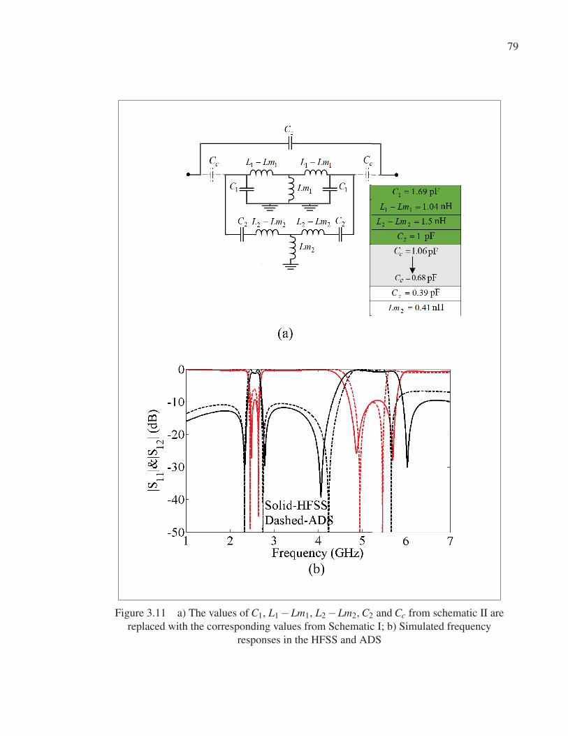
79
Figure 3.11 a) The values of C1, L1 −Lm1, L2 −Lm2, C2 and Cc from schematic II are
replaced with the corresponding values from Schematic I; b) Simulated frequency
responses in the HFSS and ADS

80
Figure 3.12 a) The value of C1, L1 −Lm1, L2 −Lm2, C2, Cc and Cz from Schematic II
are replaced with the corresponding values from Schematic I; b) Simulated frequency
responses in the HFSS and ADS

81
Figure 3.13 a) The value of C1, L1 −Lm1, L2 −Lm2, C2,Cc, Cz and Lm2 from Schematic
II are replaced with the corresponding values from Schematic I; b) Simulated frequency
responses in the HFSS and ADS

82
the simulated s-parameters of layout do not follow the same pattern of those curves which are
obtained from ideal schematic simulations.
Figure 3.14 Top view of modified D-BPF layout, dimensions are in millimeter, L1=1.4,
L2=2.3, L3=1.1, L4=1.3, L5=1.1, L6=1.7, L7=0.5, L8=0.4, L9=0.5, L10=0.7, L11=0.9,
L12=0.7, L13=1.4, L14=0.4, L15=1.56, width of lines=0.2
3.4 Conclusion
This paper has presented a fast realization methodology for transforming ideal lumped-elements
into a physical 3D LTCC layout. The entire physical realization process is explained in five
steps, which eventually leads to an excellent agreement between the S-parameters of the ideal
schematic and the layout. In this methodology, elements are designed individually and com-
bined entirely in the HFSS, and then, using a correlation strategy between HFSS and ADS the
final sizes are obtained. The main advantage of this technique is elimination of optimization
and the dimension tuning of physical elements, which reduces the time of layout realization
significantly. The proposed methodology is validated through a practical example. Schematic
of a dual-band bandpass filter operating at center frequencies of 2.4-5.2 GHz was layouted and
fabricated on an LTCC ferro A6M dielectric. LTCC was selected as a good platform for cir-

83
Figure 3.15 Photo of fabricated D-BPF
Figure 3.16 Simulated and measured frequency responses of designed D-BPF
cuit realization due to its significant properties. The EM-simulated and measured s-parameter
results validates the proposed technique.


CONCLUSION AND RECOMMENDATIONS
The size of filters and dual-band functionality can make a significant impact on dual-band wire-
less communication by replacing bulky conventional and two parallel single filters. Also, ex-
istence of synthesis procedures make easier physical circuit realizations for various demanded
microwave applications. Some features like low in-band insertion loss, good out of band rejec-
tions and acceptable return loss must be included as design considerations.
In response to the above needs, we developed novel miniaturized dual-band second order and
narrowband filter architectures in the context of lumped-element LTCC bandpass filters. In ad-
dition to high performance, we investigated the circuit realization methodologies and presented
the relevant design closed-form equations.
In the first part of this research, a novel topology of lumped-element dual-band bandpass fil-
ter was introduced. The working mechanism and nature of existing dual-band response were
explained mathematically. With the aid of developed design procedure and closed-form equa-
tions, three design example operating at frequencies 0.9-2.4GHz, 2-3GHz and 0.8-5 GHz were
presented and the values of elements calculated. The design procedure was validated by fab-
ricating 0.9-2.4GHz prototype in 5 layers LTCC dielectric. The simulation and measurement
results were provided and compared. The measured in-band insertion loss was less than 2 dB,
for the first band, and less than 1.5 dB, for the second band. The measured return loss was
better than 18dB, for the first band, and better than 22 dB, for the second band. Good out of
band rejection were obtained due to the presence of four transmission zeros located at 0.72,
1.1, 1.9 and 2.92 GHz.
In the second part, we introduced the new schematics of single- and dual-band bandpass filters
for narrowband applications, realized in LTCC. Similar to the first part, the design procedures
were provided for various filtering specifications. The single- and dual-band filters improve
out of band rejection by generating two and one transmission zeros respectively. A design

86
example of single bandpass filter operating at frequency 2.2925-2.3325 GHz were provided
and fabricated in 7 layers LTCC dielectric. The filter shows 2 dB in-band insertion loss and
return loss better than 18 dB. The two transmission zeros appear at both sides of passband and
located at 2 and 2.71 GHz frequencies. A design prototype of dual-narrow bandpass filter was
designed whereas the passbands were centered at 1.905-1.910 GHz and 2.305-2.320 GHz and
realized in 7 layers LTCC dielectric respectively. The measured insertion losses are around 1.8
dB and return losses are better than 17dB at both bands. The filter generates one transmission
zeros between two passband at 2.1GHz frequency.
In the third part, a methodology was presented for transforming of lumped-element values
from schematics into physical layouts. The methodology eliminated time consuming electro-
magnetic simulations- optimizations and provided a fast solution for obtaining the final results.
The methodology was started by designing elements individually, and then the elements were
interconnected in the final layout, and was terminated using a correlation strategy between
HFSS and ADS simulation softwares.
For the future works, we can find some research opportunities to extend this thesis. More
investigations on the presented schematics are recommended whether they can be expanded
and applied to higher order dual-band filters. Another interesting research field is design of
switchable dual-band bandpass filter . Also, some research works are recommended inten-
sively whether the structure of proposed schematics can be re-designed for tunable filtering ap-
plications with two independently passband frequencies. The performance of lumped-elements
networks are limited by SRF and low Q-factor at higher frequencies. Exploring possible tech-
niques to increase SRF values and Q-factor of lumed-element components can be considered
as one interesting research area.

BIBLIOGRAPHY
Avrillon, S., Pele, I., Chousseaud, A. & Toutain, S. (2003). Dual-band power divider based on
semiloop stepped-impedance resonators. IEEE Transactions on Microwave Theory andTechniques, 51(4), 1269–1273.
Brzezina, G. & Roy, L. (2014). Miniaturized 180◦Hybrid Coupler in LTCC for L-Band Ap-
plications. IEEE Microwave and Wireless Components Letters, 24(5), 336-338.
Brzezina, G., Roy, L. & MacEachern, L. (2009). Design enhancement of miniature lumped-
element LTCC bandpass filters. IEEE Transactions on Microwave Theory and Tech-niques, 57, 815-823.
Brzezina, G. & Roy, L. (2014). Miniaturized, Lumped-Element Filters for Customized System-
on-Package L-Band Receivers. IEEE Transactions on Components, Packaging and Man-ufacturing Technology, 4(1), 26–36.
Brzezina,G., R. L. M. L. (2009). Design Enhancement of Miniature Lumped-Element LTCC
Bandpass Filters. IEEE Transactions on Microwave Theory and Techniques, 57(4), 815-
823.
Cao, H., Yi, M., Chen, H., Liu, J., Liang, J. & Cai, W. (2014, Dec). Design of an ultra-
compact dual-band bandpass filter with CRLH resonator. 2014 International Symposiumon Antennas and Propagation Conference Proceedings, pp. 53-54.
Chen, B. J., Shen, T. M. & Wu, R. B. (2009). Dual-Band Vertically Stacked Laminated Waveg-
uide Filter Design in LTCC Technology. IEEE Transactions on Microwave Theory andTechniques, 57(6), 1554-1562.
Chen, C. C. (2005). Dual-band bandpass filter using coupled resonator pairs. IEEE Microwaveand wireless components letters, 15, 259-261.
Chen, J. X., Zhan, Y. & Xue, Q. (2015). Novel LTCC distributed-element wideband band-
pass filter based on the dual-mode stepped-impedance resonator. IEEE Transactions onComponents, Packaging and Manufacturing Technology, 5, 372-380.
Chetouah, F., Bouzit, N., Messaoudene, I., Aidel, S., Belazzoug, M. & Hammache, B.
(2016, Nov). Miniaturized rectangular dielectric resonator antenna for WCS standards.
2016 12th International Conference on Innovations in Information Technology (IIT),pp. 1-4.
Chin, K., Hung, J., Huang, C., Fu, J., Chen, B. & Chen, T. (2010). LTCC dual-band stepped-
impedance-stub filter constructed with vertically folded structure. Electronics Letters,
46(23), 1554.
Choi, B. G., Stubbs, M. G. & Park, C. S. (2003). A Ka-band narrow bandpass filter using
LTCC technology. IEEE Microwave and Wireless Components Letters, 13(9), 388-389.

88
Chu, H., Guo, Y. & Shi, X. (2011). 60 GHz LTCC 3D cavity bandpass filter with two finite
transmission zeros. Electronics Letters, 47, 324-326.
Dai, X., Zhang, X. Y., Kao, H. L., Wei, B. H., Xu, J. X. & Li, X. (2014). LTCC bandpass
filter with wide stopband based on electric and magnetic coupling cancellation. IEEETransactions on Components, Packaging and Manufacturing Technology, 4, 1705-1713.
Dai, X., Zhang, X. Y. & Cai, Z. Y. (2013, July). Compact LTCC dual-band bandpass filter
using stepped impedance resonators. 2013 Cross Strait Quad-Regional Radio Scienceand Wireless Technology Conference, pp. 109-112.
Dancila,D., R. X. T. H. A. C. D. W. & Huynen, I. (2011). 57-64 GHz seven-pole bandpass
filter Substrate Integrated Waveguide (SIW) in LTCC. 2011 IEEE MTT-S InternationalMicrowave Workshop Series on Millimeter Wave Integration Technologies, pp. 200–203.
Deng, J., Wang, B. Z. & Gan, T. (2005, July). A compact narrow bandpass filter using LTCC
technology. 2005 IEEE Antennas and Propagation Society International Symposium,
1B, 602-605 vol. 1B.
Feng, W., Gao, X., Che, W., Yang, W. & Xue, Q. (2017). LTCC Wideband Bandpass Filters
With High Performance Using Coupled Lines With Open/Shorted Stubs. IEEE Trans-actions on Components, Packaging and Manufacturing Technology, 7(4), 602-609.
He, Z., Shao, Z., You, C. J., Jiang, D. & Li, X. (2014). Design of planar narrow band
millimetre-wave filter with wide stop-band. Communication Problem-Solving (ICCP),pp. 672-674.
Hong, J. S. G. & Lancaster, M. J. (2004). Microstrip filters for RF/microwave applications.
SJohn Wiley & Sons.
Hosseini, S. E., Attari, A. R. & Pourzadi, A. (2013). A Multiband PIFA with a Slot on
the Ground Plane for Wireless Applications. International Journal of Information andElectronics Engineering, 3, 349.
Imanaka, Y. (2005). Multilayered low temperature cofired ceramics LTCC technology.
Springer Science & Business Media.
Jia Sheng Hong,Lancaster, M. (1996). Couplings of microstrip square open-loop resonators
for cross-coupled planar microwave filters. IEEE Transactions on Microwave Theoryand Techniques, 44(11), 2099–2109.
Joshi, H. & Chappell, W. J. (2006). Dual-Band Lumped-Element Bandpass Filter. IEEETransactions on Microwave Theory and Techniques, 54(12), 4169–4177.
Kapitanova, P., Kholodnyak, D., Humbla, S., Perrone, R., Mueller, J., Hein, M. A. & Vendik,
I. (2009). Right- and left-handed transmission line resonators and filters for dual-band
applications. Microwave and Optical Technology Letters, 51(3), 629-633.

89
Kim, H. T., Min, B. C., Choi, Y. H., Moon, S. H., Lee, S. M., Oh, B., Lee, J. T., Park, I. & Shin,
C. C. (1999). A compact narrowband HTS microstrip filter for PCS applications. IEEETransactions on Applied Superconductivity, 9(2), 3909-3912.
Lee, J., Lee, T. C. & Chappell, W. J. (2012). Lumped-Element Realization of Absorptive Band-
stop Filter With Anomalously High Spectral Isolation. IEEE Transactions on MicrowaveTheory and Techniques, 60(8), 2424-2430.
Li, C., Zhang, Q., Meng, Q., Sun, L., Huang, J. & Wang, Y. (2006). et al., "A high-performance
ultra-narrow bandpass HTS filter and its application in a wind-profiler radar system,"
Superconductor Science and Technology, vol. 19, p. S, 398.
Lin, K. C., Chang, C. F., Wu, M. C. & Jong, C. S. (2006). Dual-bandpass filters with serial
configuration using LTCC technology. IEEE Transactions on Microwave Theory andTechniques, 54(6), 2321–2328.
Lin, Y. C., Horng, T. S. & Huang, H. H. (2014). Synthesizing a Multiband LTCC Bandpass Fil-
ter With Specified Transmission- and Reflection-Zero Frequencies. IEEE Transactionson Microwave Theory and Techniques, 62(12), 3351–3361.
Liu, S., Xu, J. & Xu, Z. T. (2016). Compact dual-band bandpass filters using complementary
split-ring resonators with closely spaced passbands. Electronics Letters, 52, 1312-1314.
Liu, X., Katehi, L. P. B. & Peroulis, D. (2010). Novel Dual-Band Microwave Filter Using Dual-
Capacitively-Loaded Cavity Resonators. IEEE Microwave and Wireless ComponentsLetters, 20(11), 610–612.
Liu, Y., Chen, Y., Miao, X., Cui, C. & Tang, Y. (2015). Synthesis method of lumped dual-
band filters with controllable bandwidths. International Journal of RF and MicrowaveComputer-Aided Engineering, 25(1), 75-80.
Lorente, J. A., Ernst, C. & Melcon, A. A. (2013). Rigorous derivation of lossy equivalent cir-
cuit for narrowband waveguide direct-coupled-cavity filters. IET Microwaves, Antennas& Propagation, 7, 251-258.
Matthaei, G. L. (1980). Microwave filters. Impedance-Marching Networks, and CouplingStructure, 4.
Miyake, H., Kitazawa, S., Ishizaki, T., Yamada, T. & Nagatomi, Y. (1997). A miniaturized
monolithic dual band filter using ceramic lamination technique for dual mode portable
telephones. 1997 IEEE MTT-S International Microwave Symposium Digest, 2, 789-792.
Mousavi, S. H. & Kouki, A. B. (2015). High-SRF VHF/UHF Lumped Elements in LTCC.
IEEE Microwave and Wireless Components Letters, 25, 25-27.
Mousavi, S. H. & Kouki, A. B. (2014, jun). A highly compact VHF/UHF dual-band LTCC
coupler for avionic systems. 2014 IEEE MTT-S International Microwave Symposium(IMS2014), pp. 1–4.

90
Oshima, S., Wada, K., Murata, R. & Shimakata, Y. (2010). Multilayer Dual-Band Bandpass
Filter in Low-Temperature Co-Fired Ceramic Substrate for Ultra-Wideband Applica-
tions. IEEE Transactions on Microwave Theory and Techniques, 58(3), 614–623.
Pourzadi, A., Attari, A. R. & Majedi, M. S. (2012). A Directivity-Enhanced Directional
Coupler Using Epsilon Negative Transmission Line. IEEE Transactions on MicrowaveTheory and Techniques, 60(11), 3395-3402.
Pourzadi, A., Isapour, A. & Kouki, A. (2019). Design of Compact Dual-Band LTCC Second-
Order Chebyshev Bandpass Filters Using a Direct Synthesis Approach. IEEE Transac-tions on Microwave Theory and Techniques, 67(4), 1441-1451.
Rezaee, M. & Attari, A. R. (2014, oct). A novel dual mode dual band SIW filter. 2014 44thEuropean Microwave Conference, pp. 853–856.
Schindler, M. J. & Tajima, Y. (1989). A novel MMIC active filter with lumped and transversal
elements. IEEE Transactions on Microwave Theory and Techniques, 37(12), 2148-2153.
Shafique, M. F. & Robertson, I. D. (2011). Laser prototyping of multilayer LTCC microwave
components for system-in-package applications. IET Microwaves, Antennas Propaga-tion, 5(8), 864-869.
Shao, J. Y. & Lin, Y. S. (2015). Narrowband coupled-line bandstop filter with absorptive
stopband. IEEE Transactions on Microwave Theory and Techniques, 63, 3469-3478.
Shen, T., Chen, C., Huang, T. & Wu, R. (2009, Dec). Design of lumped rat-race cou-
pler in multilayer LTCC. 2009 Asia Pacific Microwave Conference, pp. 2120-2123.
doi: 10.1109/APMC.2009.5385258.
Shen, W., Yin, W., Sun, X. & Wu, L. (2013). Substrate-Integrated Waveguide Bandpass Filters
With Planar Resonators for System-on-Package. IEEE Transactions on Components,Packaging and Manufacturing Technology, 3(2), 253-261.
Su, L. & Tzuang, C. K. C. (2012). A narrowband CMOS ring resonator dual-mode active
bandpass filter with edge periphery of 2% free-space wavelength. IEEE Transactions onMicrowave Theory and Techniques, 60, 1605-1616.
TAMURA, M., ISHIZAKI, T., HASHEMI, M. R. M. & ITOH, T. (2010). Approach
of Metamaterial-Based Quarter-Wave Resonator and Its Application to Very Compact
LTCC Bandpass Filter. IEICE Transactions on Electronics, E93.C(7), 1078-1088.
Tamura, M., Yang, T. & Itoh, T. (2011). Very Compact and Low-Profile LTCC Unbalanced-
to-Balanced Filters With Hybrid Resonators. IEEE Transactions on Microwave Theoryand Techniques, 59(8), 1925-1936.
Tang, C. W. & You, S. F. (2006). Using the technology of low temperature co-fired ceramic
to design the dual-band bandpass filter. IEEE Microwave and Wireless ComponentsLetters, 16(7), 407-409.

91
Tang, C. W., You, S. F. & Liu, C. (2006). Design of a dual-band bandpass filter with low-
temperature co-fired ceramic technology. IEEE Transactions on Microwave Theory andTechniques, 54(8), 3327-3332.
Tang, C. (2007). Development of LTCC bandpass filters with transmission zeros. ElectronicsLetters, 43(21), 1149-1150.
Turgaliev, V., Kholodnyak, D. & Vendik, I. (2013). Small-size dual-band filters on capacitively
loaded cavities. 2013 European Microwave Conference, pp. 660-663.
V. Turgaliev,D. Kholodnyak, J. M. & Hein, M. (2015). Small-size low-loss bandpass filters on
substrate-integrated waveguide capacitively loaded cavities embedded in low tempera-
ture co-fired ceramics. Journal of Ceramic Science and Technology, 6(4), 305-314.
Wang, J., Xu, X. & Zhang, G. (2013). 60 GHz dual-band bandpass filter using LTCC. Elec-tronics Letters, 49(16), 1001–1002.
Xu, J., Wu, W. & Wei, G. (2016a). Novel dual-band bandpass filter and reconfigurable filters
using lumped-element dual-resonance resonators. IEEE Transactions on MicrowaveTheory and Techniques, 64, 1496-1507.
Xu, J. X., Zhang, X. Y., Zhao, X. L. & Xue, Q. (2016b). Synthesis and implementation of
LTCC bandpass filter with harmonic suppression. IEEE Transactions on Components,Packaging and Manufacturing Technology, 6, 596-604.
Xu, J., Wu, W. & Wei, G. (2016c). Novel Dual-Band Bandpass Filter and Reconfigurable
Filters Using Lumped-Element Dual-Resonance Resonators. IEEE Transactions on Mi-crowave Theory and Techniques, 64(5), 1496–1507.
Xu, X., Wang, J. & Zhang, G. (2013). 60 GHz dual-band bandpass filter using LTCC. Elec-tronics Letters, 49, 1001-1002.
Yang, T., Tamura, M. & Itoh, T. (2010). Super Compact Low-Temperature Co-Fired Ceramic
Bandpass Filters Using the Hybrid Resonator. IEEE Transactions on Microwave Theoryand Techniques, 58(11), 2896–2907.
Yatsenko, A., Orlenko, D., Sakhnenko, S., Sevskiy, G. & Heide, P. (2007). A Small-Size
High-Rejection LTCC Diplexer for WLAN Applications Based on a New Dual-Band
Bandpass Filter. 2007 IEEE/MTT-S International Microwave Symposium, pp. 2113-
2116.
Yeung, L. K. & Wu, K. L. (2003). A compact second-order LTCC bandpass filter with two
finite transmission zeros. IEEE Transactions on Microwave Theory and Techniques,
51(2), 337-341.
Zhang, X. Y., Dai, X., Kao, H. L., Wei, B. H., Cai, Z. Y. & Xue, Q. (2014). Compact LTCC
bandpass filter with wide stopband using discriminating coupling. IEEE Transactionson Components, Packaging and Manufacturing Technology, 4, 656-663.

92
Zheng, S. Y., Yongle Wu,Yuanxin Li, Y. L. & Long, Y. (2014). Dual-Band Hybrid Coupler
With Arbitrary Power Division Ratios Over the Two Bands. IEEE Transactions onComponents, Packaging and Manufacturing Technology, 4(8), 1347–1358.
Zheng, Y. & Sheng, W. (2017). Compact Lumped-Element LTCC Bandpass Filter for Low-
Loss VHF-Band Applications. IEEE Microwave and Wireless Components Letters,
27(12), 1074-1076.
Zhou, B., Cheng, C., Yan, L., Zhou, N., Cao, Y., Tang, Q., Li, Q., Ma, Q., Song, Z., Li,
S., Wang, Z. & Hu, S. (2016, Oct). Miniaturized lumped-element LTCC quadrature
hybrid with harmonics suppression. 2016 IEEE International Conference on UbiquitousWireless Broadband (ICUWB), pp. 1-3.
Zhou, C., Guo, Y., Yan, S. & Wang, Z. (2011). Dual-band UWB filter with LTCC technology.
Electronics Letters, 47(22), 1230.
Zhou, K., Zhou, C. & Wu, W. (2018). Substrate-Integrated Waveguide Dual-Band Filters With
Closely Spaced Passbands and Flexibly Allocated Bandwidths. IEEE Transactions onComponents, Packaging and Manufacturing Technology, 8(3), 465-472.
Zhu, H. & Abbosh, A. M. (2016). Single- and Dual-Band Bandpass Filters Using Coupled
Stepped-Impedance Resonators With Embedded Coupled-Lines. IEEE Microwave andWireless Components Letters, 26(9), 675-677.