novel high-κ dielectrics for next-generation electronic
TRANSCRIPT
OPEN
ORIGINAL ARTICLE
Novel high-κ dielectrics for next-generation electronicdevices screened by automated ab initio calculations
Kanghoon Yim1,2, Youn Yong1,2, Joohee Lee1,2, Kyuhyun Lee1,2, Ho-Hyun Nahm3,4, Jiho Yoo5, Chanhee Lee5,Cheol Seong Hwang1,2 and Seungwu Han1,2
As the scale of transistors and capacitors in electronics is reduced to less than a few nanometers, leakage currents pose a
serious problem to the device’s reliability. To overcome this dilemma, high-κ materials that exhibit a larger permittivity and band
gap are introduced as gate dielectrics to enhance both the capacitance and block leakage simultaneously. Currently, HfO2 is
widely used as a high-κ dielectric; however, a higher-κ material remains desired for further enhancement. To find new high-κmaterials, we conduct a high-throughput ab initio calculation for band gap and permittivity. The accurate and efficient
calculation is enabled by newly developed automation codes that fully automate a series of delicate methods in a highly
optimized manner. We can, thus, calculate 41800 structures of binary and ternary oxides from the Inorganic Crystal Structure
Database and obtain a total property map. We confirm that the inverse correlation relationship between the band gap and
permittivity is roughly valid for most oxides. However, new candidate materials exhibit interesting properties, such as large
permittivity, despite their large band gaps. Analyzing these materials, we discuss the origin of large κ values and suggest design
rules to find new high-κ materials that have not yet been discovered.
NPG Asia Materials (2015) 7, e190; doi:10.1038/am.2015.57; published online 12 June 2015
INTRODUCTION
The dielectric insulator is a key component in microelectronic devicessuch as the central processing unit (CPU), dynamic random-accessmemory (DRAM) and flash memory. The basic function of thedielectric material is to enhance the capacitive coupling betweenadjacent metals and semiconductors, although it should also suppressthe leakage current between electrodes, which undermines the energyconsumption (in CPU and DRAM) or long-term reliability (in flashmemory). In past decades, silicon dioxide (SiO2) has been used as anarchetypical dielectric material because it allows for defect-free, high-quality thin-film growth. As the integration level of microelectronicdevices is currently exponentially increasing, the thickness of SiO2 hasdecreased to maintain the device performance. However, if the SiO2
layer becomes thinner than ~ 1 nm, the leakage current due to thequantum tunneling effect begins to dominate,1 which causes seriousproblems in power consumption and device performance. Thistechnical obstacle has been overcome by replacing SiO2 with insulatorsthat possess high dielectric constants (high-κ).1,2 With high-κ dielec-trics, the dielectric thickness can be increased at the same capacitance,thereby suppressing the leakage current.3 Currently, the favored high-κdielectrics are HfO2 (as the gate dielectric in CPU),2 ZrO2 (as thecapacitor dielectric in DRAM)4 and Al2O3 (as the blocking oxide incharge-trap flash memory).3
In addition to a large dielectric constant, the high-κ dielectric isrequired to have a large band gap (Eg) to suppress the charge injectionfrom electrodes into dielectrics that cause the leakage current. There-fore, the ideal high-κ dielectrics should possess both large Eg and κ.Notably, when Eg and κ of well-known oxides are plotted (seeFigure 1), the trade-off relation is clearly noticeable. That is, materialsare abundant with large Eg (4~8 eV) or high κ (4~20); however,no material has been discovered that satisfies both conditionssimultaneously. Because this observation is based on a limited set ofmaterials, one may question whether a material possessing both largeEg and κ may indeed exist if the search space is expanded.Obtaining material information on Eg and κ, particularly the static
dielectric constant, would be prohibitive if only experimental mea-surements were utilized. However, with the recent advances incomputational methods and facilities, it is now feasible to computeab initio various physical properties of the bulk phase in a relativelyshort period. Recently, several attempts have been made to find anoptimal functional material using high-throughput computationalscreening.5–8 The machine-learning approach presented by G.Pilania9 is a more accelerated approach to predict properties of largenumbers of polymers; however, the prediction accuracy for Eg and κ islow for extending the method to other systems. In this study, weperform ab initio calculations on ~ 1800 oxides (except for 3dtransition metal oxides) that cover most binary and ternary oxides
1Department of Materials Science and Engineering, Seoul National University, Seoul, South Korea; 2Research Institute of Advanced Materials, Seoul National University, Seoul,South Korea; 3Center for Correlated Electron Systems, Institute for Basic Science (IBS), Seoul, South Korea; 4Department of Physics and Astronomy, Seoul National University,Seoul, South Korea and 5Platform Technology Lab., SAIT, Samsung Materials Research Complex, Yeong Tong-gu, Gyeonggi-do, South KoreaCorrespondence: Professor S Han, Department of Materials Science and Engineering, Seoul National University, 30-422, 1 Gwanak-ro, Gwanak-gu, Seoul 151-744, South Korea.E-mail: [email protected] 15 November 2014; revised 24 February 2015; accepted 14 April 2015
NPG Asia Materials (2015) 7, e190; doi:10.1038/am.2015.57& 2015 Nature Publishing Group All rights reserved 1884-4057/15www.nature.com/am

identified to date and suggest novel candidate high-κ dielectricssuitable for each device type. To this end, we set up computationalmachinery that automatically fetches structures from the database,prepares input files and reliably performs the ab initio calculations.
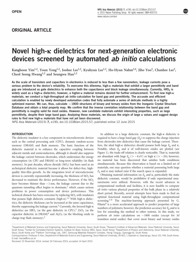
MATERIALS AND METHODSFigure 2 presents a brief scheme of our automation strategy for calculating Egand κ. First, all of the structures that contain specific cations are collected fromthe Inorganic Crystal Structure Database.10 We exclude 3d transition metalatoms because the electronic correlation effects are strong and Eg is moderate(o3 eV). The structures are further screened to avoid duplicative calculationson the same structure. The structures with partial atomic occupation areexcluded because of the difficulty in computational modeling. In addition tothe structures that are stable at ambient conditions, we consider structures thatare characterized under high-temperature or high-pressure conditions, pro-vided that they are theoretically stable at zero temperature and pressureconditions, because the metastable structures can exist at ambient conditionsthrough doping11 or in nanocrystalline states.12 The atomic positions and latticeparameters are then relaxed, and the theoretical equilibrium structures areobtained. For the computational code, the Vienna Ab Initio SimulationPackage13 is adopted as the core engine for the ab initio calculations. Regardingthe exchange-correlation functional between electrons, we employ the general-ized gradient approximation (GGA)14 for Eg and local density approximation(LDA)15 for κ. Because GGA and LDA underestimate the band gap, we alsoperform a hybrid-functional calculation for the band-edge points identified byGGA. The detailed procedure for each step is provided in the Methods section.The reliability of the present automation procedure is confirmed by comparingthe extant experimental data with previous calculations.
Structural relaxationAll experimental structures should first be relaxed theoretically. This step ismandatory because when computing a dielectric constant, the structures areassumed to be at the local equilibrium. The k-points in the first Brillouin zoneare carefully and automatically sampled such that the total energy and stresstensor components are converged within 5meV per atom and 10 kbar,respectively. The energy cutoff for the plane-wave basis set is selected basedon the atomic species and pseudopotential types. The structural relaxation isperformed until the atomic force and stress tensor are reduced to below 0.02eVÅ− 1 and 5 kbar, respectively. Many structures reported at high-temperatureor high-pressure conditions often have higher symmetry compared with low-temperature phases. When these structures are relaxed with the symmetrymaintained, the final structures often possess unstable phonon modes. Weexclude these structures from consideration as new high-κ candidates becauseof their stability issue.
Computation of band gapWe first computed energy levels along the lines connecting the high-symmetryk-points within GGA.16 On the basis of the results, the k-points correspondingto the valence top and conduction minimum are determined. Because the bandgap underestimation is severe in the semilocal functional, we additionallyperform a hybrid-functional (HSE06) calculation17 (without further structuralrelaxation) and calculate the energy levels at the band-edge k-points identifiedby GGA (this scheme is called HSE@GGA hereafter). This process assumes thatthe band structure rigidly shifts upon application of the hybrid functional.Supplementary Figure S1 in the Supplementary Information shows that theband structure from the hybrid functional is approximately a rigid shift of theGGA result. By adopting the HSE@GGA scheme, we could significantly reducethe computational cost compared with the full hybrid-functional calculations.For oxides that include heavy elements such as Tl, Pb and Bi, the spin-orbitcoupling is included in computing Eg.To ensure the reliability of the present scheme, test calculations on several
oxides are performed and compared with the experiment and previous GGAcalculations (see Figure 3a). The estimated energy gaps are in good agreementwith the experiment, although sizeable errors of up to 1 eV are noticeable foroxides with Eg larger than ~4 eV. These errors are due to the fixed fraction ofthe exact exchange term in the HSE06 functional, which should be increased inthe large-gap materials.18 This finding implies that more sophisticated methodssuch as GW calculations can be utilized to obtain more precise values of Eg. Wenote that the GW calculations are too expensive to be incorporated into thehigh-throughput screening. In addition, it is not yet known which level of GWapproximations can be universally applied to every class of oxides.19 Never-theless, the accuracy of HSE@GGA is sufficient to screen promising dielectricsin the present study.
Computation of dielectric constantTo compute the electronic permittivity, the linear-response method based onthe density functional perturbation theory is used to obtain Born effectivecharges and phonon modes at the zone center.20 Because the linear-responsecomputation is sensitive to the k-point sampling, we double the k-point densityalong each direction. The static dielectric constant (e0ab) is then calculated usingthe following formula:
e0ab ¼ eNab þ 4pO
Xm
Z�maZ
�mb
o2m
; ð1Þ
2
3
4
5
6
7
8
9
10
0 20 40 60 80 100 120
Ene
rgy
gap
(eV
)
Ideal high-κ materialsIdeal high-κ materials
Static dielectric constant
Figure 1 The experimental band gap and dielectric constant for well-knownoxides. The property region ideal for dielectrics is also shown.
OHf
InorganicCrystal StructureDatabase
Propertydatabase
Select elements
Stucturalrelaxation
Ab initiocalculations
Pre-screeningof
structures
Static dielectricconstant
Band gap
Initial structures
Conduction
Valence
Equilibrium structures
Figure 2 Schematic automation strategy to collect computational data onthe band gap and static dielectric constant. The initial structures collectedfrom the ICSD were filtered for the ensuing ab initio computations.
High-κ dielectrics for next-generation electronic devicesK Yim et al
2
NPG Asia Materials
where e0ab, Ω, ωm and Z�m denote the dielectric tensor contributed by electrons,
the unit-cell volume, the frequency of the infrared-active phonon with the
mode number of m and the mode-effective Born effective charges, respectively.
The subscripts α and β in equation (1) indicate the directions. The dielectric
constant (κ) is obtained by averaging the diagonal components of e0ab. Thetheoretical κ of some oxides determined by GGA and LDA are compared with
the experiment (see Figure 3b). The mean absolute errors for materials with
κo30 are 2.06 and 1.37 for the GGA and LDA results, respectively. The GGA
results exhibit larger errors than those of LDA because the ionic part of κ is
sensitive to the low-frequency phonon modes that are significantly softened
when the lattice parameters are expanded in GGA. Therefore, we employ LDA
for computing κ.
Computational costThe average computational cost was ~ 70 CPU hours per structure on the 24-
core cluster. The most time-consuming part was the hybrid-functional
calculation in the HSE@GGA scheme (50%) followed by the density functional
perturbation theory calculations for the dielectric constant (27%). The structure
relaxation and band-edge searching consumed ~15% and 8% of the total
computational time, respectively.
RESULTS
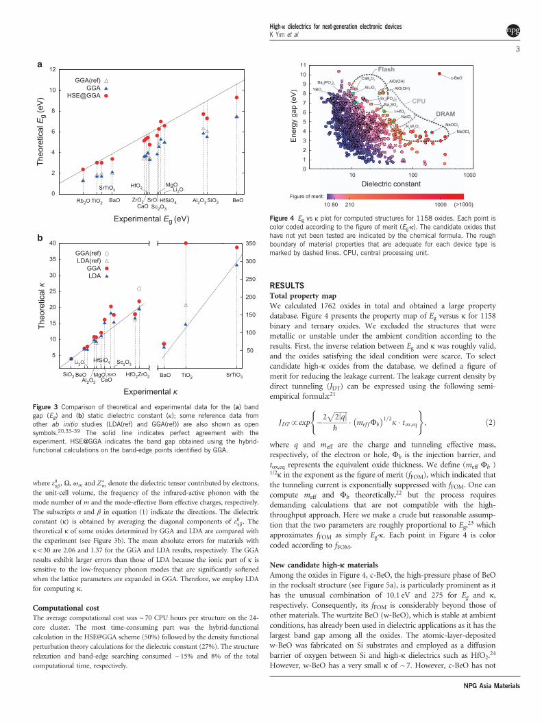
Total property mapWe calculated 1762 oxides in total and obtained a large propertydatabase. Figure 4 presents the property map of Eg versus κ for 1158binary and ternary oxides. We excluded the structures that weremetallic or unstable under the ambient condition according to theresults. First, the inverse relation between Eg and κ was roughly valid,and the oxides satisfying the ideal condition were scarce. To selectcandidate high-κ oxides from the database, we defined a figure ofmerit for reducing the leakage current. The leakage current density bydirect tunneling (JDT) can be expressed using the following semi-empirical formula:21
JDTpexp �2ffiffiffiffiffiffiffiffi2 qj jp_
� mef fFb
� �1=2k � tox;eq( )
; ð2Þ
where q and meff are the charge and tunneling effective mass,respectively, of the electron or hole, Фb is the injection barrier, andtox,eq represents the equivalent oxide thickness. We define (meff Фb )1/2κ in the exponent as the figure of merit (fFOM), which indicated thatthe tunneling current is exponentially suppressed with fFOM. One cancompute meff and Фb theoretically,22 but the process requiresdemanding calculations that are not compatible with the high-throughput approach. Here we make a crude but reasonable assump-tion that the two parameters are roughly proportional to Eg,
23 whichapproximates fFOM as simply Eg·κ. Each point in Figure 4 is colorcoded according to fFOM.
New candidate high-κ materialsAmong the oxides in Figure 4, c-BeO, the high-pressure phase of BeOin the rocksalt structure (see Figure 5a), is particularly prominent as ithas the unusual combination of 10.1 eV and 275 for Eg and κ,respectively. Consequently, its fFOM is considerably beyond those ofother materials. The wurtzite BeO (w-BeO), which is stable at ambientconditions, has already been used in dielectric applications as it has thelargest band gap among all the oxides. The atomic-layer-depositedw-BeO was fabricated on Si substrates and employed as a diffusionbarrier of oxygen between Si and high-κ dielectrics such as HfO2.
24
However, w-BeO has a very small κ of ~ 7. However, c-BeO has not
50
100
150
200
250
300
350
BaO TiO2 SrTiO3
5
10
15
20
25
30
35
40
SiO2 BeOAl2O3
MgOCaO
SrO HfO2ZrO2
Theo
retic
al κ
Experimental κ
GGA(ref)LDA(ref)
GGALDA
~ ~~ ~
GGA(ref)GGA
HSE@GGA
0
2
4
6
8
10
12
Rb2O TiO2 BaO ZrO2CaO
SrOSc2O3
HfSiO4 Al2O3 SiO2 BeO
Theo
retic
al E
g (e
V)
Experimental Eg (eV)
Figure 3 Comparison of theoretical and experimental data for the (a) bandgap (Eg) and (b) static dielectric constant (κ); some reference data fromother ab initio studies (LDA(ref) and GGA(ref)) are also shown as opensymbols.20,33–39 The solid line indicates perfect agreement with theexperiment. HSE@GGA indicates the band gap obtained using the hybrid-functional calculations on the band-edge points identified by GGA.
Figure of merit:
0
1
2
3
4
5
6
7
8
9
10
11
10 100 1000
Ene
rgy
gap
(eV
)
Dielectric constant
Flash
DRAM
CPU
80 210 100010 (>1000)
Figure 4 Eg vs κ plot for computed structures for 1158 oxides. Each point iscolor coded according to the figure of merit (Eg·κ). The candidate oxides thathave not yet been tested are indicated by the chemical formula. The roughboundary of material properties that are adequate for each device type ismarked by dashed lines. CPU, central processing unit.
High-κ dielectrics for next-generation electronic devicesK Yim et al
3
NPG Asia Materials

been applied in microelectronic devices to date as far as we are aware.The origin of the large κ of c-BeO is its soft optical phonon mode(~3.5 THz), wherein the Be and O atoms vibrate in opposite directions(see Figures 5a and b). In c-BeO, the Be–O bond length is longer thanthat in w-BeO by 0.11 Å, which softens the optical phonon mode. Thecomputed total energy indicates that c-BeO is less stable than w-BeOby 0.483 eV per atom. The large energy difference implies that c-BeOwould be difficult to stabilize under ambient conditions. However, wepay attention to the experiments in Adelmann et al.25, Kita et al.26 andTsipas et al.27, which indicate that the high-temperature phases of
HfO2 and ZrO2 can be synthesized as thin films by external doping orstrain. More importantly, the doped phases possessed increaseddielectric constants, as predicted by theory.28 Therefore, we reasonablyexpect that c-BeO can be stabilized by doping or strain and will exhibitphysical properties similar to the present calculations.Except for c-BeO, we could not find any outstanding high-κ
dielectrics with either Eg or κ larger than those of the HfO2 thinfilms currently used in CPU or DRAM (Eg ~ 6.0 eV and κ~20–25; seet-HfO2 in Figure 4). Nevertheless, we identified several candidates thatare noteworthy and list them in Table 1. These materials could beimportant in the future as the main material shifts from Si to Ge andGaAs and a more diverse selection of gate dielectrics is highlydemanded to meet chemical conditions that are different from Si.Here we exclude oxides that have been studied previously. In the lastcolumn of Table 1, we mark the appropriate device type according tothe material properties; for CPU and DRAM devices, the internationaltechnology roadmap of semiconductors states that further devicescaling requires higher-κ dielectrics with κ430.29 We note thecandidate high-κ materials that satisfy this condition and have largerfFOM than that of t-HfO2 (fFOM~210). We also limited Eg44 eV forCPU and Eg43 eV for DRAM, considering that the ideal Φb should beat least 41.5 eV. For the blocking oxides used in flash memory, largevalues of Eg are more crucial than large κ to satisfy the more stringentleakage current specification (o~10− 9 Acm− 2) compared withDRAM (o~10− 7 Acm− 2) and CPU (o~10− 1 Acm− 2). We, there-fore, impose the condition of Eg46 eV and fFOM480, which is largerthan the values for Al2O3, the currently favored high-κ blocking oxidein the charge-trap flash memory. The total candidate lists includingthose for DRAM and Flash are provided in Tables 2 and 3,respectively. For the gate dielectric for CPU, we further consider thatthe stability of high-κ/Si interfaces is important to prevent theunintentional oxidation of the Si substrate. One metric of oxidestability is the formation energy of oxygen vacancies (Evac) because itreflects the strength of metal–oxygen bonding. The computed Evacs forthe candidate materials are listed in Table 1. Because the Evac of SiO2 is5.6 eV, oxides with Evac values larger than this value may form a stableinterface with Si. For example, it is known that ZrO2 (Evac= 5.1 eV)exhibits a stability issue on Si substrates,30 whereas HfO2 (Evac= 6.9eV) is stable. This behavior is reflected in selecting candidate oxidesfor CPU in Table 1. ΔE per atom in Table 1 denotes the total energy
Figure 5 (a) The unit-cell structure of c-BeO and the lowest phonon modeindicated by arrows. The frequency of this mode (ω) is also noted. (b) Thephonon dispersion curve of c-BeO. The lowest phonon mode (threefolddegenerate) is marked by a circle. The unit-cell structure of (c) NbOCl3 and(d) Na2SO4. The lowest phonon modes that are responsible for most of κ areshown in each structure with the vibrational directions indicated by arrows.
Table 1 New candidate materials suitable for high-κ dielectrics selected from Figure 3
Name ICSD κ Eg (eV) fFOM ΔE per atom (eV) Evac(eV) CPU DRAM Flash
c-BeO 163825 274.8 10.11 2780 0.483 6.62 ✓ ✓ ✓
NbOCl3 26471 343.4 3.43 1176 0.002 4.91 ✓
NbOCl3 412071 208.8 3.90 815 0 4.81 ✓
δ-AlO(OH) 166337 32.78 8.09 265 0.031 4.65 ✓ ✓
NaIO3 202679 48.84 4.94 241 0 2.11 ✓
δ-AlO(OH) 166331 28.82 8.03 231 0.026 7.08 ✓ ✓ ✓
K2W2O7 67284 63.70 3.43 219 0 3.93 ✓
Na2SO4 66554 20.70 6.89 143 0.004 3.24 ✓
Sr3(PO4)2 30635 17.90 7.18 129 0 5.06 ✓
CaB4O7 412710 11.64 8.48 99 0 6.25 ✓
AlLiO2 28288 10.64 8.01 85 0.024 7.05 ✓
Ba3(PO4)2 30634 12.02 7.03 85 0 5.06 ✓
YBO3 100015 11.33 7.05 80 0 6.22 ✓
Abbreviation: ICSD, Inorganic Crystal Structure Database.ΔE per atom is the relative energy with respect to theoretically the most stable structure. Evac is the formation energy of neutral oxygen vacancy. The suitable application for each material is markedin the last three columns.
High-κ dielectrics for next-generation electronic devicesK Yim et al
4
NPG Asia Materials

per atom relative to the most stable phase identified from the presentcomputation and indicates the relative thermal stability of thegiven phase.
DISCUSSION
In Figures 5c and d, the structures of two candidate oxides, AlO(OH)and Na2SO4, are displayed together with the lowest phonon mode,indicated by arrows. These structures exhibit the two representativefeatures of high-κ ternary oxides. In the lowest phonon modes of AlO(OH) (Figure 5c), cations vibrate within the octahedral cage formed byanions. In contrast to face-sharing octahedra in Al2O3, H
+ ions in AlO(OH) lead to corner sharing, which softens the vibrational mode of Al3+. NbOCl3 in Table 1 also has a similar feature of cationic vibrationwithin the corner-sharing octahedra. However, all of the other ternaryoxides in Table 1 have another common feature, which can berepresented by Na2SO4 in Figure 5d: they usually contain non-metaloxygen units such as (SO4)
2−, (PO4)3− and (IO3)
−. These units form arigid bond in the compounds, whereas the other type of cation isloosely bound to oxygen and yields soft phonon modes (see Na atoms
in Figure 5d). Furthermore, we find that the unblocked cation channelis critical for a large dielectric constant. For example, two polymorphsof Na2SO4 have common orthorhombic phases but slightly differentatomic arrangements with a crystal symmetry of Cmcm and Pbnm,respectively (see Supplementary Figure S2 in SupplementaryInformation). The coordination number and oxidation state of eachatom are similar, and Eg is thus almost the same. However, the two κvalues significantly differ (Cmcm: 20.7 vs Pbnm: 5.9).For the Cmcm structure, as shown in Figure 5d, all of the cations in
the soft mode vibrate coherently along certain passages without beingblocked by other species of atoms. However, such an unblockedchannel does not exist in the Pbnm phase. Consequently, the Na atomsoscillate in rather random directions, and the contributions todielectric polarization cancel each other out, resulting in smaller κ.Note that the ionic conduction of Na+ can cause device instability31.However, considering the lower ionic conductivity in the Cmcmstructure compared with that for other phases32, we cautiously believethat the high-κ phase of Na2SO4 could be employed in microelectronicdevices.On the basis of these observations, high-κ ternary oxides that
simultaneously exhibit large Eg and κ might be identified through twomodels: (1) cationic vibration within the corner-sharing octahedralcage of anions and (2) channeled structures formed by a combinationof metal ions and various non-metal oxide units. Considering thenumerous possible combinations to form ternary oxides, we expectthat several ideal dielectric materials that have these features could beidentified in the future.
Table 2 All high-κ candidate materials for DRAM and CPU from the
present property database, which satisfy fFOM4210, and Eg43 eV
(for DRAM) or Eg44 eV (for CPU)
Name ICSD Space group κ Eg (Ev) fFOM
BeO 163825 225 274.80 10.11 2780
NbOCl3 26471 136 343.40 3.43 1176
SrTiO3 201256 221 288.12 3.01 869
NbOCl3 412071 113 208.83 3.90 815
NaNbO3 247316 33 163.36 3.94 643
NaTaO3 88377 127 167.76 3.55 595
AgTaO3 40830 161 180.95 3.15 570
AgTaO3 40831 167 177.85 3.16 563
SrTiO3 182762 140 162.94 3.09 504
Li4CO4 245400 8 62.39 7.83 489
CdTiO3 62150 62 134.28 3.45 464
CdTiO3 51698 26 132.24 3.50 462
CdTiO3 262711 33 133.47 3.46 461
KTaO3 56440 221 131.87 3.33 439
Y2Ti2O7 15633 227 101.98 4.02 410
Cd2Ta2O7 75605 227 112.80 3.53 399
NaTaO3 88375 62 96.60 3.96 382
TiO2 202241 136 122.10 3.02 369
NaTaO3 980 62 92.71 3.98 369
PbHfO3 89326 55 72.14 3.78 273
AlO(OH) 166337 58 32.78 8.09 265
AlO(OH) 166345 58 32.42 8.14 264
SrHfO3 161595 127 49.92 5.19 259
Ag2Ta4O11 180734 167 61.83 4.11 254
BaZrO3 43136 221 54.57 4.62 252
PbZrO3 31154 32 65.13 3.82 249
NaIO3 202679 62 48.84 4.94 241
BiTaO4 97423 52 56.17 4.23 238
PbHfO3 174106 55 62.69 3.79 238
PbHfO3 33194 32 60.85 3.84 234
AlO(OH) 166331 31 28.82 8.03 231
HfTe3O8 9078 206 44.14 5.12 226
ZrO2 93031 137 38.53 5.71 220
K2W2O7 67284 14 63.70 3.43 219
Sr2Ta2O7 16388 36 50.30 4.25 214
Abbreviations: CPU, central processing unit; ICSD, Inorganic Crystal Structure Database.
Table 3 All high-κ candidate materials for flash memory application
from the present property database, which satisfy fFOM480 and
Eg46 eV
Name ICSD Space group κ Eg (eV) fFOM
BeO 163825 225 275 10.11 2780
AlO(OH) 166345 58 32.4 8.14 264
AlO(OH) 166331 31 28.8 8.03 231
HfO2 173966 137 34.3 6.12 210
LaYO3 419666 62 25.8 6.32 163
Na2SO4 66554 63 20.7 6.89 143
Sr3(PO4)2 30635 166 17.9 7.18 129
YAlO3 4115 62 16.1 7.36 119
MgSiO3 171911 62 15.5 7.49 116
YOCl 60586 129 15.2 6.53 99
CaB4O7 412710 31 11.6 8.48 99
MgAl2O4 157186 62 14.2 6.80 96
Ba2SiO4 28476 62 15.0 6.21 93
B2O3 51575 152 10.5 8.57 90
Mg4O3(OH)2 95470 164 14.2 6.28 89
Ba3P4O13 280908 2 13.0 6.85 89
B2O3 36066 144 10.4 8.57 89
Li3OBr 67265 221 11.6 7.61 88
Mg(OH)2 79031 164 13.4 6.59 88
MgSiO3 172736 63 13.1 6.57 86
Y2(Si2O7) 164148 2 13.3 6.41 85
AlLiO2 28288 166 10.6 8.01 85
YOF 76426 129 12.9 6.57 85
Ba3(PO4)2 30634 166 12.0 7.03 85
SrB4O7 95300 31 9.12 9.03 82
BaSO4 33730 62 10.4 7.79 81
Abbreviation: ICSD, Inorganic Crystal Structure Database.
High-κ dielectrics for next-generation electronic devicesK Yim et al
5
NPG Asia Materials
In summary, we screened ~ 1800 binary and ternary oxides usinghigh-throughput ab initio calculations of the band gap and staticdielectric constant with the aim to find new candidate high-κdielectrics that can be used in various microelectronic devices suchas CPU, DRAM and flash memory. From the obtained propertydatabase, we generated a materials map of the band gap versus staticdielectric constant and identified new candidate materials that havenot been considered in previous studies. From the detailed analysis onthe atomic structure and phonon mode, we identified key factors thatcorrelate with the large dielectric constant. By suggesting newcandidate high-κ materials and developing a large material propertydatabase covering most binary and ternary oxides, the present workwill contribute greatly to selecting functional oxides that are optimalfor specific applications. An automated high-throughput study onoxygen vacancy defects in oxides is also in progress.
CONFLICT OF INTERESTThe authors declare no conflict of interest.
ACKNOWLEDGEMENTS
This research was supported by the EDISON program(NRF-2012M3C1A6035307). The computations were performed at the KISTIsupercomputing center (KSC-2014-C3-012).
1 Kingon, A. I., Maria, J.-P. & Streiffer, S. K. Alternative dielectrics to silicon dioxide formemory and logic devices. Nature 406, 1032–1038 (2000).
2 Robertson, J. High dielectric constant gate oxides for metal oxide Si transistors. Rep.Prog. Phys. 69, 327–396 (2006).
3 Lee, C.-H., Hur, S.-H., Shin, Y.-C., Choi, J.-H., Park, D.-G. & Kim, K. Charge-trappingdevice structure of SiO2 /SiN/high-k dielectric Al2O3 for high-density flash memory.Appl. Phys. Lett. 86, 152908 (2005).
4 Kim, S. K., Lee, S. W., Han, J. H., Lee, B., Han, S. & Hwang, C. S. Capacitors with anequivalent oxide thickness of o0.5 nm for nanoscale electronicsemiconductor memory. Adv. Funct. Mater. 20, 2989–3003 (2010).
5 Hautier, G., Miglio, A., Ceder, G., Rignanese, G.-M. & Gonze, X. Identification anddesign principles of low hole effective mass p-type transparent conducting oxides. Nat.Commun. 4, 2292 (2013).
6 Fujimura, K., Seko, A., Koyama, Y., Kuwabara, A., Kishida, I., Shitara, K., Fisher, C. A.J., Moriwake, H. & Tanaka, I. Accelerated materials design of lithium superionicconductors based on first-principles calculations and machine learning algorithms. Adv.Energy Mater 3: 8 980–985 (2013).
7 Bennett, J. W. & Rabe, K. M. Integration of first-principles methods and crystallographicdatabase searches for new ferroelectrics: Strategies and explorations. J. Solid StateChem. 195, 21–31 (2012).
8 Curtarolo, S., Hart, Gus, L. W., Nardelli, M. B., Mingo, N., Sanvito, S. & Levy, O. Thehigh-throughput highway to computational materials design. Nat. Mater. 12,191–201 (2013).
9 Pilania, G., Wang, C., Jiang, X., Rajasekaran, S. & Ramprasad, R. Acceleratingmaterials property predictions using machine learning. Sci. Rep. 3, 2810 (2013).
10 Karlsruhe, F. I. Z. Inorganic Crytal Structure Database, Available at http://icsd.fiz-karlsruhe.de.
11 Lee, C.-K., Cho, E., Lee, H.-S., Hwang, C. S. & Han, S. First-principles study on dopingand phase stability of HfO2. Phys. Rev. B 78, 012102 (2008).
12 McHale, J. M., Auroux, A., Perrotta, A. J. & Navrotsky, A. Surface energies andthermodynamic phase stability in nanocrystalline aluminas. Science 277, 788 (1997).
13 Kresse, G. & Hafner, J. Ab initio molecular dynamics for liquid metals. Phys. Rev. B 47,558 (1993).
14 Perdew, J. P., Burke, K. & Ernzerhof, M. Generalized gradient approximationmade simple. Phys. Rev. Lett. 78, 1396 (1997).
15 Ceperley, D. M. & Alder, B. J. Ground state of the electron gas by a stochastic method.Phys. Rev. Lett. 45, 566 (1980).
16 Setyawan, W. & Curtarolo, S. High-throughput electronic band structure calculations:Challenges and tools. Comput. Mater. Sci. 49, 299 (2010).
17 Heyd, J., Scuseria, G. E. & Ernzerhof, M. J. Hybrid functionals based on a screenedCoulomb potential. Chem. Phys. 118, 8207–8215 (2003).
18 Marques, M. A. L., Vidal, J., Oliveira, M. J. T., Reining, L. & Botti, S. Density-basedmixing parameter for hybrid functionals. Phys. Rev. B 83, 035119 (2011).
19 Kang, Y., Kang, G., Nahm, H.-H., Cho, S.-H., Park, Y. S. & Han, S. GW calculations onpost-transition-metal oxides. Phys. Rev. B 89, 165130 (2014).
20 Lee, C.-K., Cho, E., Lee, H., Seol, K. & Han, S. Comparative study of electronicstructures and dielectric properties of alumina polymorphs by first-principles methods.Phys. Rev. B 76, 245110 (2007).
21 Yeo, Y.-C. MOSFET gate leakage modeling and selection guide for alternative gatedielectrics based on leakage considerations. IEEE Trans. Electron Dev. 50:4 1027 (2003).
22 Robertson, J. Band offsets of wide-band-gap oxides and implications for futureelectronic devices. J. Vac. Sci. Technol. B 18, 1785 (2000).
23 Hinkle, C.L., Fulton, C., Nemanich, R.J. & Lucovsky, G. A novel approach fordetermining the effective tunneling mass of electrons in HfO2 and other high-Kalternative gate dielectrics for advanced CMOS devices. Microelectron. Eng. 72,257–262 (2004).
24 Yum, J. H., Bersuker, G., Akyol, T., Ferrer, D.A., Lei, M., Park, K. W., Hudnall, T. W.,Downer, M. C., Bielawski, C. W., Yu, E. T., Price, J., Lee, J. C. & Banerjee, S. K.Epitaxial ALD BeO: efficient oxygen diffusion barrier for EOT scaling and reliabilityimprovement. IEEE Trans. Electron Dev. 58, 4384–4392 (2011).
25 Adelmann, C., Tielens, H., Dewulf, D., Hardy, A., Pierreux, D., Swerts, J., Rosseel, E. X.,Shi, E., Van Bael, M. K., Kittl, J.A. & Van Elshochta, S. Atomic Layer Deposition of Gd-Doped HfO2 Thin Films. J. Electrochem. Soc 157, 4 (2010).
26 Kita, K., Kyuno, K. & Toriumi Akira. Permittivity increase of yttrium-dopedHfO2 through structural phase transformation. Appl. Phys. Lett. 86, 102906(2005).
27 Tsipas, P., Volkis, S. N., Sotiropoulos, A., Galata, S. F., Mavrou, G., Tsoutsou, D.,Panayiotatos, Y., Dimoulas, A., Marchiori, C. & Fompeyrine, J. Germanium-inducedstabilization of a very high-k zirconia phase in ZrO2/GeO2 gate stacks. Appl. Phys. Lett.93, 082904 (2008).
28 Zhao, X. & Vanderbilt, D. First-principles study of structural, vibrational, and latticedielectric properties of hafnium oxide. Phys. Rev. B 65, 233106 (2002).
29 International Technology Roadmap for Semiconductors (2013) http://www.itrs.net/,accessed on May 2014.
30 Fulton, C. C., Cook, T. E. Jr., Lucovsky, G. & Nemanich, R. J. Interface instabilitiesand electronic properties of ZrO2 on silicon (100). J. Appl. Phys. 96, 2665(2004).
31 Snow, E. H., Grove, A. S., Deal, B. E. & Sah, C. T. Ion transport phenomena ininsulating films. J. Appl. Phys. 36, 1664 (1965).
32 Choi, B.-K. & Lockwood, D. J. Ionic conductivity and the phase transitions in Na2SO4.Phys. Rev. B 40, 4683 (1989).
33 Moakafi, M., Khenata, R., Bouhemadou, A., Khachai, H., Amrani, B., Rached, D. &R’erat, M. Electronic and optical properties under pressure effect of alkali metal oxides.Eur. Phys. J. B 64, 35–42 (2008).
34 Labat, F., Baranek, P., Domain, C., Minot, C. & Adamo, C. Density functional theoryanalysis of the structural and electronic properties of TiO2 rutile and anatase polytypes:Performances of different exchange-correlation functionals. J. Chem. Phys. 126,154703 (2007).
35 Jaffe, J. E., Bachorz, R. A. & Gutowski, M. Low-temperature polymorphs of ZrO2 andHfO2: a density-functional theory study. Phys. Rev. B 72, 144107 (2005).
36 Xiong, K., Robertson, J. & Clark, S. J. Behavior of hydrogen in wide band gap oxides. J.App. Phys. 102, 083710 (2007).
37 Rignanese, G.-M. Dielectric properties of crystalline and amorphous transition metaloxides and silicates as potential high-κ candidates: the contribution of density-functional theory. J. Phys. Condens. Matter 17, R357–R379 (2005).
38 Lukačević, I. High-pressure lattice dynamics and thermodynamics in BaO. Phys. StatusSolidi B 248, 1405–1411 (2011).
39 Lee, B., Lee, C.-K., Hwang, C.S. & Han, S. Influence of exchange-correlationfunctionals on dielectric properties of rutile TiO2. Curr. Appl. Phys. 11,S293–S296 (2011).
This work is licensed under a Creative CommonsAttribution 4.0 International License. The images or
other third party material in this article are included in the article’sCreative Commons license, unless indicated otherwise in the creditline; if the material is not included under the Creative Commonslicense, userswill need to obtain permission from the license holder toreproduce the material. To view a copy of this license, visit http://creativecommons.org/licenses/by/4.0/
Supplementary Information accompanies the paper on the NPG Asia Materials website (http://www.nature.com/am)
High-κ dielectrics for next-generation electronic devicesK Yim et al
6
NPG Asia Materials