novel joint chip sampling and phase synchronization...
TRANSCRIPT

I. J. Communications, Network and System Sciences, 2008, 2, 105-206 Published Online May 2008 in SciRes (http://www.SRPublishing.org/journal/ijcns/).
Copyright © 2008 SciRes. I. J. Communications, Network and System Sciences, 2008, 2, 105-206
Novel Joint Chip Sampling and Phase Synchronization Algorithm for Multistandard UMTS Systems
Youssef SERRESTOU1, Kosai RAOOF2, Joël LIÉNARD2
1 LCIS-INPG, 50 Rue Barthélémy de Laffemas, 26902 cedex, Valence, France 2 GIPSA-LAB, CNRS UMR 5216, 961 Rue de Houille Blanche, 38402 St. Martin d’Hères, France
E-mail: [email protected], [email protected] Abstract CDMA Timing and phase offsets tracking remain as one of considerable factors that influence the performances of communication systems. Many algorithms are proposed to solve this problem. In general, these solutions process separately the chip sampling offset and phase rotation. In addition, most of proposed solutions can not assure a compromise between robustness criteria and low complexity for implementation in real time applications. In this paper we present an efficient algorithm for chip sampling and phase synchronization. This algorithm allows estimating and correcting jointly in real time, sampling instant and phase errors. The robustness and the low complexity of this algorithm are evaluated, firstly by simulation and then tested by real experimentation for UMTS standard. Simulation results show that the proposed algorithm provides very efficient compensation for sampling clock offset and phase rotation. A real time implementation is achieved, based on TigerSharc DSP, while using a complete UMTS transmission-reception chain. Experimental results show robustness in real conditions. Keywords: Synchronization, DS-CDMA, UMTS, Joint Estimation, Early-late Loop, Phase Locked Loop 1. Introduction Code Division Multiple Access (CDMA) system offers several advantages such as robustness to multi-path fading channel and multiple access properties [1]. Thanks to these advantages, CDMA are adopted in high data rate applications such as UMTS standard (Universal Mobile Telecommunication System), and it is a good candidate for future applications, such as the 4th generation phone mobile and wireless LAN [2]. However, the performance of such systems is affected by the time sampling offsets and phase rotation, due to many factors such as channel fading, multipath problem, clock imperfection, etc.
Recent research works are interested in solving this problem of synchronization for different applications [3–7]. In general the synchronization techniques of DS-CDMA systems can achieve synchronization in two distinct steps: acquisition step and tracking step. The acquisition step, or the initial synchronization step, involves in determining the timing/phase offsets of the incoming signal to within a specified range known as the
pull-in region of tracking loop [8–11]. Upon the successful completion of the acquisition step, the tracking step refines and maintains synchronization. When the problem of tracking is treated, generally, phase offset tracking is omitted or treated separately with a more complex computation than delay tracking [3–7, 12, 13]. The tracking step is based on recursive estimation of timing/phase error and feedback correction. So the performance of synchronization depends greatly on the properties of estimators and on the precision of correctors. To estimate time delay the conventional delay lock loop (DLL) has been extensively used. In a DLL the received signal is cross-correlated with an early and a late copy of a pilot signal. The proposed tracking algorithm is inspired from the concept of lock loop to establish estimation [14]. So the complex correlation function of the received signal and pilot signal is computed in three points (which corresponds to original, early and late copy of the pilot signal). This computation allows estimating jointly the time delay and the phase rotation. A second order filters are used to update the estimation. For the feedback corrector, an interpolator [15] is used to find the sample at the estimated instant;

106 Y. SERRESTOU ET AL.
Copyright © 2008 SciRes. I. J. Communications, Network and System Sciences, 2008, 2, 105-206
the used interpolator gives good compromises between precision and real time application. The correction of phase rotation consists of multiplying the received signal by the complex exponential of estimated phase [14,15].
In this study we are interested in implementing the tracking algorithm in a complete transmission-reception chain. The aim of this chain is to demonstrate the feasibility of a reconfigurable software radio communication system based on UMTS standard. The tracking algorithm was adapted to UMTS specifications [16–20]. In simulation context, the performances of these algorithms were evaluated in the presence of a fading and additive white Gaussian noise channel (AWGN). In the case of a multipath channel, acquisition and tracking blocks synchronize the signal of the high power path. One block within the complete chain contains an algorithm for channel estimation [21,22].
DS-CDMA was adopted in UMTS standard as an access scheme. And for radio access there are two modes, FDD (Frequency Division Duplex) and TDD (Time Division Duplex), for operating with paired and unpaired bands respectively. The possibility to operate in either FDD or TDD mode allows an efficient use of the available spectrum according to the frequency allocation in different regions. The modulation scheme is QPSK, and because of the CDMA nature the spreading (and scrambling) process is closely associated with modulation. To spread transmitted signal different families of spreading codes are used. For separating channels from the same source, orthogonal codes are derived with code tree structure. And for separating different cells in FDD mode Gold codes with 10 ms period (38400 chips at 3.84 Mcps) are used and for TDD mode we implement codes with period of 16 chips and midamble sequences of different length depending on the environment [16-20]. Our tracking algorithm has adopted for both UMTS modes TDD and FDD. Simulation has allowed evaluating the performances and determining suitable parameters for implementation. The final real time implementation was accomplished with a 32-bit TigerSharc DSP.
The rest of this paper is organised as follows. Section 2 presents the algorithm context. The basic aim of this section is to present the theoretical models of transmitted/received signals in UMTS and the communication channel that we consider. So the different phases of signal forming (spreading, scrambling, channel effects, noise) are described. In section 3, the mathematical model of the tracking algorithm is presented, as well as it’s adaptation for UMTS-FDD and UMTS-TDD standard. We focus on the estimators’ performances with theoretical demonstration ended by simulation to show the efficiencies of this algorithm. Section 4 describes simulation platform and result analysis. The implementation and experiment results are detailed in section 5. Some conclusions are given in section 6.
2. Base-Band Signal Model in UMTS 2.1. Introduction Our tracking algorithm tries to maintain synchronization of the received signal by a UMTS terminal. So we are interested in the downlink mode (base station to terminal). We introduce some useful notions for modeling the base-band signal in the context of UMTS standard. These notions are specified and described in detail in the 3rd Generation Partnership Project (3GPP); see [16–20].
The access scheme is Direct-Sequence Code Division Multiple Access (DS-CDMA). There are two radio access modes, FDD (Frequency Division Duplex) and TDD (Time Division Duplex), which allows operating with paired and unpaired bands respectively. The modulation scheme is QPSK, and different families of spreading codes are used. These codes are OVSF (orthogonal variable spreading factor). And for separating different cells in FDD mode Gold codes (scrambling codes) with 10 ms period (38400 chips at 3.84 Mega chip per second Mcps) are used and for TDD mode we use codes with period of 16 chips and midamble sequences of different length depending on the environment [16–20]. In FDD mode the uplink and downlink transmissions use two different radio frequencies. In TDD mode the uplink and downlink transmissions are modulated over the same frequency by using synchronized time intervals.
In both modes the transmitted signal is decomposed into radio frames. A radio frame has duration of 10 ms and contains 38400 chips at the rate of 3.84 Mcps. It is divided into 15 slots, and every slot contains 2560 chips.
A physical channel is therefore defined as a simple code (or number of codes used to spread this channel), additionally in TDD mode the sequence of time slots completes the definition of a physical channel.
The information rate, in terms of symbols/s, varies with the spreading factor (number of chips by symbol). Spreading factors (noted SF) are from 512 to 4 for FDD downlink, and from 16 to 1 for TDD downlink. Thus the respective modulation symbol rates vary from 960 k symbols/s to 15 k 7.5 k symbols/s for FDD downlink, and for TDD the momentary modulation symbol rates shall vary from 38400 symbols/s to 240 k symbols/s. 2.2. Signal Model in UMTS-FDD Mode In FDD mode a practical fixed rate channel with predefined symbol (1+j) sequence is transmitted within each frame, this common pilot channel (CPICH), use the first spreading code in tree with spreading factor equal to 256. The proprieties of this channel allows receiver to identify cell’s location. In our work we have used this channel as signal pilot to estimate the time delay and

NOVEL JOINT CHIP SAMPLING AND PHASE SYNCHRONIZATION 107 ALGORITHM FOR MULTISTANDARD UMTS SYSTEMS
Copyright © 2008 SciRes. I. J. Communications, Network and System Sciences, 2008, 2, 105-206
phase rotation. Let N physical channels be transmitted with QPSK
symbols{ }jd nl ±±= 1)( , n denotes the channel number
and l represents the symbol number. Every symbol is transformed to a sequence of chips
by spreading operation. SF “spreading factor” denotes the spreading code length, i.e. the number of chip per symbol. The combination of all channels is scrambled by the same code that we denoted SC. The following combined signal is obtained:
))(()( ,)(
ckSFlk
SF
k
nSFk
N
l
nl
N
nn TSFlktSCCdGtd
n
n
n
n
⋅⋅+−= ⋅+∑∑∑ δ
(1)
where Gn is the gain of channel n, { }1,1, −∈nSFk n
C is
the kth chips in spreading code used to spread the nth channel, SFn is the spreading factor used for the nth channel and { }1,1−∈kSC denotes the kth chip in scrambling code. Tc is chip duration and δ(.) is the Dirac
delta function. A root raised cosine impulse filter, denoted he(t), is
used to shape this signal for transmission. For propagation channel, we adopt a fading channel
with AWGN noise. Its impulse response is modeled as follow:
))(()()( )( ttetth tjc τδα ϕ −= (2)
where α(t) is the fading of propagation channel given from Jake’s Doppler spectrum, τ(t) is the time delay, and φ(t) represents the random phase shift introduced by propagation, and it will be added to another phase shift which is caused by the imperfections of receiver-transmitter oscillators.
The received signal is filtered by a root raised cosine with impulse response hr(t). Then it is sampled with a period Te. We denote by OSF=Tc/Te the over sampling factor, i.e. number of samples per chip. Let g(t) be the convolution product Cr0(t)*hc(t)*hr(t), the received signal may be written as:
{ })())()(()()( ,,)(
, tmTTlSFkOSFttgSCCaGtetyn
kk
n SF
k
OSF
meeklSFk
nSFk
N
lnl
N
nn
tFDDr ηταϕ +−+−−= ∑∑∑∑ + (3)
{ })())()(()()(
))256()(()1()()()(
,,)(
0
256
256)(
0,
tmTTlSFkOSFttgSCCaGtety
where
mTTlkOSFttgSCjGtetyty
n
kk
n
n
SF
k
OSF
meeklSFk
nSFk
N
lnl
N
nn
tr
CPICH
k
OSF
meelk
N
lcpich
t
channelother
rFDDr
ητα
τα
ϕ
ϕ
+−+−−=
−+−−++=
∑∑∑∑
∑∑∑
+
+
44444444444444 344444444444444 21321
(4)
{Noise
data
OSF
leee
N
n i
ki
kkn
midamble
OSF
leee
L
n
kn
data
OSF
leee
N
n i
ki
kkn
tjkTDDr
ttlTOSFnTOSFTitgswd
tlTOSFnTOSFTitgm
tlTOSFnTOSFTitgswdetty
k
m
k
)())(16)1((.
))(16)1((
))(16)1((.)()(
1
00
16
1
)2,(
1
01
1
00
16
1
)1,()(,
ητ
τ
τα ϕ
+⎥⎥⎥
⎦
⎤
−−−−−
+−−−−−
+⎢⎢⎢
⎣
⎡
−−−−−=
∑∑ ∑
∑∑
∑∑ ∑
−
== =
−
==
−
== =
444444444444 3444444444444 21
4444444444 34444444444 21
444444444444 3444444444444 21
(5)
where η(t) is an additive Gaussian noise, Te is the sampling time (Tc=OSF.Te), Tc is the chip duration, and φ(t) is the global phase shift introduced by propagation channel and oscillators imperfections. In FDD the received signal contains the CPICH symbols, so we can separate the signal in two parts; one part contains CPICH
symbols and the other part contains the other transmitted channels, which allows us to write equation (4).
Equation (4) gives us the received signal model in baseband for UMTS-FDD, the calculus and demonstrations in the next sections are based on this model.

108 Y. SERRESTOU ET AL.
Copyright © 2008 SciRes. I. J. Communications, Network and System Sciences, 2008, 2, 105-206
2.3. Signal Model in UMTS-TDD Mode The UMTS TDD physical channel is a combination of two data fields, a midamble, and a guard period. There are two burst types proposed in [20], namely burst type 1 and 2. As illustrated in Figure 1, both types have the same length of 2560 chips and are terminated by a guard period of 96 chips in order to avoid overlapping with consecutive time slots. Burst type 1 has a longer midamble (512 chips) suitable for cases where long training periods are required for adaptation and tracking. The midamble code is used as signal pilot for tracking algorithm.
Figure 1. Two burst types
With the same notation as the previous sub-section B, the received signal in TDD modes will be written as described in (4). In equation (4), d(k,1) denotes the data symbols transmitted before the midamble and d(k,2) denotes the data symbols after the midamble. The combination of the user specific channelization and cell specific scrambling codes can be seen as a user and cell specific spreading code, with chip values, are denoted by Si
k in (4). 3. Digital Joint Synchronization Algorithm 3.1. Introduction The sampling instant of the received signal is fluctuated, and the phase is shifted because of the channel effects, the reception clock imperfections, and receiver-transmitter oscillators’ imperfections. The received signal needs synchronization to extract the transmitted sequences. So that synchronization is divided into two phases, acquisition phase and tracking phase. Acquisition is the first step that the mobile phone does, known as “cell search” in UMTS standard. It consists finding the beginning of signal (top frame and top slot) within a half chip precision. This operation allows also finding the cell’s parameters. The tracking step updates the phase and the sampling instant continuously in time. In this section we will detail the algorithm used in tracking phase. The developed algorithm consists of four steps, as shown on Figure1, assuming that the baseband signal is obtained by radio frequency down conversion followed by a linear filtering system, and the acquisition is done correctly.
3.2. Timing Correction We look to extract from the received samples the correct transmitted samples. To perform this operation the received signal will be interpolated at the estimated correct instant. The following formula presents the fundamental equation for digital interpolation [23]:
[ ] [ ]
⎥⎦
⎤⎢⎣
⎡=⇒+⎥
⎦
⎤⎢⎣
⎡=
+⋅−=+= ∑=
e
ikeke
e
ii
ek
N
iekekki
TkTmTT
TkTkT
TihTimxTmykTy
µ
µµ )()())(()(0
where x is the received signal, Te is the theoretical sampling period, Ti represents the fluctuated sampling period, and h(t) is the impulse response of interpolated filter. The interpolation coefficients are modified in function of the delay µk.
In our work we estimate the delay time µk then we adapt the interpolator coefficients. N is the number of interpolator coefficients, and [] denotes integer part function.
In literature there are many methods to interpolate digital signal: linear interpolation, polynomial interpolation, piecewise-parabolic interpolation and some others [23,24]. The choice of an interpolator depends on two criterions: precision and complexity. In our study we have chosen a truncated cardinal sine wave. In UMTS the over-sampling factor is reconfigurable, and to assure real time criteria the number of interpolators’ coefficients depends on the over-sampling factor. 3.3. Phase Correction The second step is to correct the phase shift. The interpolated complex samples (I and Q) are multiplied by complex exponential of the estimate phase.
kjii ekTykTz ϕ̂)()( −=
where y(kTi) is the interpolated complex samples and kϕ̂ is the estimated phase. For phase correction, in order to find the phase reference, the sign of the real and imaginary parts allows to find the reference region in the QPSK plan. 3.4. Joint Estimation of Delay and Phase Now we are arrived in one of the principal point in our work, the correction of the sampling instant and phase require the knowledge of time delay and phase shift. We use a procedure that allows us estimating jointly these parameters. These measurements are filtered by a loop filters, then they are used by interpolation and phase correction blocks. We use two different methods for estimation in the TDD and FDD modes. In the following

NOVEL JOINT CHIP SAMPLING AND PHASE SYNCHRONIZATION 109 ALGORITHM FOR MULTISTANDARD UMTS SYSTEMS
Copyright © 2008 SciRes. I. J. Communications, Network and System Sciences, 2008, 2, 105-206
sub-sections we explain these methods. 3.4.1. Estimation for UMTS-FDD Mode The sampling instant delay and the phase shift are estimated over one symbol duration, Ts=SF*Tc, in order to correct the next symbol timing. The sampling instant is corrected by interpolation and the phase is corrected by complex multiplication between received signal and estimated phase.
We use as a pilot signal the corresponding scrambling code, because the CPICH channel is a copy of the scrambling code. So the received signal is divided into successive symbols (256 chips i.e. 256.OSF samples), and we calculate the correlation between each symbol and the original, early, and late copy of the corresponding symbol.
Let yr,s be the sth symbol of received signal (described in equation (4)) and SCs represents the sequence of scrambling code, which was aligned in transmission with this part of the signal. The time delay and phase shift are supposed to be constant during one symbol period, then without correction of signal we obtain the following correlation function at instant ε:
{ {
}
{Noise
ationautocorrelSC
delay
SC
ssymbolCPICH
cpich
shiftphasage
s
fadingSCy sjGes
sssr)())(()1()()()(
'_
)(,,0
ετεγαεγεγ ϕ Ν+−++=4434421321
(6) The spreading code is orthogonal, that means the
correlation function of two codes is equal to zero. The first term is negligible. The scrambling code local auto-correlation function can be approximated by a triangular function:
csc T
εεγ −≈ 1)(
For 2,0,2
cc TT−=ε we have:
)0())(1)(1()(
)0())(()1()()0(
)(
)(
=+−+≈
=+−+≈=
ετα
εταε
ϕ
ϕ
NT
sjGse
NsrjGser
ccpich
s
SCcpichs
r
)2/())(211)(1()(
)2/())(2
()1()()2
(
)(
)(
cc
cpichs
cc
SCcpichsc
TNT
sjGse
TNsTrjGseTrr
−++−+≈
−+−−+≈−=
τα
ταε
ϕ
ϕ
)2/())(211)(1()(
)2/())(2
()1()()2
(
)(
)(
cc
cpichs
cc
SCcpichsc
TNT
sjGse
TNsTrjGseTrr
−+−−+≈
+−+≈=
τα
ταε
ϕ
ϕ
(7) We observe that these measurements contain
information about the time delay and the phase shift; our
idea is to extract this information from these measurements. Real and imaginary parts of one-time correlation function allow estimating the phase rotation φ(s). The early and late correlation functions give estimation of the time delay τ(s). Let define the measurements ∆τ and ∆φ, as the sampling instant delay and phase shift. And Re(.), Im(.) are the real and imaginary part function of a complex number.
),()](sin[)(1)(2
))0(Im())0(Re()( ,, ,,
τϕηϕτα
εεϕ
+⎟⎟⎠
⎞⎜⎜⎝
⎛−=
=−==∆
sT
sGs
rrs
ccpich
SCySCy ssrssr
),()](cos[)(211)(2
))2
(Im())2
(Re()(
1
,,1 ,,
τϕηϕτα
εε
+⎟⎟⎠
⎞⎜⎜⎝
⎛−−=
=+==∆
sT
sGs
TrTrs
ccpich
cSCy
cSCy ssrssr
),()](cos[)(211)(2
))2
(Im())2
(Re()(
2
,,2 ,,
τϕηϕτα
εε
+⎟⎟⎠
⎞⎜⎜⎝
⎛−−=
−=+−==∆
sT
sGs
TrTrs
ccpich
cSCy
cSCy ssrssr
⎪⎪⎪
⎩
⎪⎪⎪
⎨
⎧
+⎟⎟⎠
⎞⎜⎜⎝
⎛−−+≅
∆−∆=∆
+⎟⎟⎠
⎞⎜⎜⎝
⎛−≅∆
⇒
),()](cos[)(21)(
21)(2
)(
),()(sin)(1)(2)(
2
21
1
τϕηϕττα
τϕηϕταϕ
sT
sT
sGs
s
sT
sGss
cccpich
x
ccpich
(8)
Let )(ˆ sτ be the estimation of the sampling instant delay and )(ˆ sϕ is the estimation of phase shift, with a correction loop. Then the previous equations become:
⎪⎪⎪⎪
⎩
⎪⎪⎪⎪
⎨
⎧
+−
⋅⎟⎟⎠
⎞⎜⎜⎝
⎛ −−−
−+≅∆
+
−⎟⎟⎠
⎞⎜⎜⎝
⎛ −−≅∆
),()](ˆ)(cos[
)()(ˆ21)()(ˆ
21)(2)(
),(
)](ˆ)(sin[)()(ˆ1)(2)(
2
1
τϕηϕϕ
ττττα
τϕη
ϕϕτταϕ
ss
Tss
TssGss
ssT
ssGss
cccpichx
ccpich
(9) If the system of estimation and correction converge
correctly, the time delay and phase error must converge to zero. In this condition:
[ ]( ) 1)(ˆ)(cos
)(ˆ)()(ˆ)(sin≈−
−≈−ss
ssssϕϕ
ϕϕϕϕ
With this condition, equation (8) gives the estimation of delay and phase as follows:
[ ]
),()()(ˆ)(4)(
),()(ˆ)()(2)(
2
1
τϕηττα
τϕηϕϕα
τ
ϕ
+−
≅∆
+−≅∆
e
cpich
cpich
Tss
OSFGs
s
ssGss
(10)

110 Y. SERRESTOU ET AL.
Copyright © 2008 SciRes. I. J. Communications, Network and System Sciences, 2008, 2, 105-206
where OSF is the over sampling factor, i.e. the number of samples per chip, Tc is the chip duration and Te is the sampling period. Hence, Tc=OSF.Te. Gcpich is the channel gain of CPICH [17,18], and α(s) is the fading of the propagation channel. Always, we suppose that the fading is invariant for symbol duration (Ts=SF.Tc=SF.OSF.Te). These measurements are filtered by a second order filter that we discuss it in the next section. Now we will establish these measurements in the case of TDD mode. 3.4.2. Estimation for UMTS-TDD Mode We are going here to explain how we estimate sampling instant delay and phase shift in TDD mode. In this mode we process slot by slot the 2560 chips i.e. 2560.OSF samples. This is different from FDD mode where we process symbol by symbol. We have chosen this way because in the TDD mode we don’t have a permanent channel with a known spreading code. In addition the TDD mode will be used when we have a good propagation channel conditions. In this case we can consider that the delay time and the phase shift are constant over one slot duration. For these raisons we use midamble code as a signal pilot to achieve synchronisation. So we calculate correlation function between the received midamble and the transmitted midamble in three points (codes aligned, the midamble code shifted to right and to left by OSF/2 samples). These measurements are filtered to estimate time delay and phase shift. Estimation of the sampling instant delay and the phase shift over actual slot is used to correct the next slot. The sampling instant is corrected by interpolation and the phase is corrected by complex multiplication between received signal and complex exponential of the estimated phase.
With the same notations and calculus as in the previous sub-section concerning FDD, we can derive the measurements of phase and delay errors as follows:
( )
),()()(ˆ)(2)(
),()(ˆ)()()(
2
1
τϕηττα
τϕηϕϕα
τ
ϕ
+−
≅∆
+−≅∆
eTss
OSFss
ssss (11)
These parameters are filtered by a second order filters
in order to estimate phase and delay. The structure of these filters is the same as in FDD mode. But filters’ coefficients are different. This difference comes from the difference in the gain, sampling frequency and updating time period. We study in the following section these loop filters.
3.5. Closed Loop Estimation
A Second-order loops should be able to track delay and phase offset as long as the values of the coefficients is carefully chosen.
So, the ∆τ can be filtered by a second order filter with
λ1 and λ2 as coefficients. The output of the filter is used to determine the interpolator impulse response to find the correct sample. In FDD mode the interpolator response is updated every symbol (256 chips), but in TDD mode is updated every slot (2560 chips). The interpolation filter is updated for each symbol or slot (s) which is used to correct the sampling instant error for the next symbol or slot (s+1). Here we describe how a time loop filter updates time delay:
)()(
21
11
ss
ss
kss
τ
τ
λεελεµµ
∆+=∆++=
+
+ (12)
where µ is the estimated instant to be used by interpolator and ε is the error of estimation.
With a similar structure the measurement ∆φ is filtered by a second-order filter with two coefficients γ1 and γ2. The output of the filter is used to correct the phase by complex multiplication. The phase is updated every symbol in FDD mode and every slot in TDD mode. So the calculated phase in symbol or slot (s) is used to correct the phase of the next symbol or slot (s+1). The following equation shows how a phase loop filter updates the phase:
)()(
21
11
ss
ss
sss
ϕ
ϕ
γδδ
γδφφ
∆+=
∆++=
+
+ (13)
where φ is the estimated instant to be used by phase corrector and δ is the estimation error.
From equations (10) and (12), we can derive the expression of sampling instant estimation:
⎟⎟⎠
⎞⎜⎜⎝
⎛+
−+=+ )()(ˆ)()()(1 s
TsssAzF
ess ητταµµ ττ
where Aτ depends on the mode (TDD or FDD):
and Fτ (z) is the loop filter transfer function:
1
12
1 1)( −
−
−+=
zzzF λ
λτ
For the phase estimation, we find the same equation, but filter coefficients are different:
⎟⎟⎠
⎞⎜⎜⎝
⎛+
−+=+ )()(ˆ)()()(1 s
TsssAzF
ess ηϕϕαφφ ϕϕ
again Aφ depends on the mode (TDD or FDD) :

NOVEL JOINT CHIP SAMPLING AND PHASE SYNCHRONIZATION 111 ALGORITHM FOR MULTISTANDARD UMTS SYSTEMS
Copyright © 2008 SciRes. I. J. Communications, Network and System Sciences, 2008, 2, 105-206
and Fφ (z) is the loop filter transfer function:
1
12
1 1)( −
−
−+=
zzzF δδϕ
Estimator properties must be studied to determine
filter coefficients. We observe that the time loop filter and phase loop filter have the same structure; in addition they have the same structure for both of modes FDD and TDD. So, we are studying the closed loop estimation in the general case using this filter structure. In what follows, we illustrate estimator properties in order to demonstrate how filters’ coefficients are determined.
Figure 2 shows the diagram of a closed loop. We denote by m the parameter that we want to estimate and correct.
Figure 2. Estimation loop
The open loop transfer function of this system can be written as:
)1()2()()(
1212
121
+−+−+−+
=mmm
mmmm AAzAz
AAzAzH
where Am1 and Am2 are defined as :
2
11
ββ
mm
mm
AAAA
==
2
We calculate the coefficients Am1 and Am2 for the case
of a stable system. In order to have two complex conjugate poles, we should have ( ) 04 2
21 <− mm AA , and
⎪⎩
⎪⎨⎧
>
<
02
2
21
m
mm
AAA
(14)
If the first condition is verified then the poles of Hm(z) are:
⎪⎪⎩
⎪⎪⎨
⎧
+−−−=
+−+−=
242
242
22
11*
22
11
mmmm
mmmm
AAjAp
AAjAp
(15)
We have a second order system; this system can be
stable if the modules of its poles are smaller than one. These conditions imply that
( ) 0442 122
21
21 <−⇒<+−− mmmmm AAAAA
and with the first condition the criteria of stability becomes:
⎪⎩
⎪⎨⎧
<<
<<
402
2
212
m
mmm
AAAA (16)
In order to achieve good estimation, we must choose
filters’ coefficients which minimize the estimation error (the residual error after convergence). With this criterion we can calculate the appropriate coefficients. From the structure of the closed loop estimation (Figure 4), the variance of the estimation error can be calculated as follows:
))(*)(1var()ˆvar( tthA
mm m η=−
where hm(t) is the impulse response of the open loop filter, and η(t) denotes an additive Gaussian noise. Let
)(*)()( ttht m ηη =′ defines the filtered noise and N0 is the power spectral density of the noise η(t). So the power spectral density of the noise η’(t) is:
22
20 )()( fj
m ezHANf π
η ==Γ ′
The variance of the noise η’(t) is relied to the power
spectral density by the following relation:
fdezHANfdft
R
fjmR ∫∫ ==Γ=′ ′
2220 )()())((var π
ηη
By proceeding to a variable change, the integral can
be calculated on the unit circle in Z plane.
dzzpzp
zzpzpz
zzAjAN
mm
m
mm
mm ∫ −−−
−−−
=)1()1(
1)()(2
)(var **2
210
πε
(17)
where zm is the zero and pm is the pole the transfer function. The function to be integrated have four poles,

112 Y. SERRESTOU ET AL.
Copyright © 2008 SciRes. I. J. Communications, Network and System Sciences, 2008, 2, 105-206
two of them are out of the unit circle in Z plane, so by using the residue theorem we can calculate this integral then we obtain:
( )( )[ ]mmmm
mm
zpezpppA
ANm )(411
)1(1
1)(var 22
2222
20 1 ℜ−++
−−=ε
(18)
To find filters’ coefficients with efficient estimator, the variance of the estimator must be optimized. There is a region of coefficients that allows to an accepted variance relative to Cramer-Rao bound. Also in simulation we have found that for these values the variance of estimation error is minimal. From these values we can calculate the different filters’ coefficients.
In the FDD mode, and for the time loop filter (TLF) we fix the coefficient as follows:
OSFA 2
=τ , CPICHG
OSF•=
15.01λ and
CPICHGOSF•
=05.0
2λ
and for the phase loop filter (PLF):
CPICHGA 2=ϕ , CPICHG
3.01 =δ and
CPICHG1.0
2 =δ
If we don’t know the gain of the channel CPICH
(which is less than one) we fix it to one. Even for this case we are sure that our system is stable and the estimation error stay minimal.
In the TDD mode, for the time loop filter (TLF) we fix the coefficients to the following values:
OSFA 2
=τ , OSF3.01 =λ and OSF•= 1.02λ
and for the phase loop filter (PLF):
1=ϕA , 6.01 =δ and 2.02 =δ
4. Simulation Platform In order to test the proposed algorithm and to determine all necessary parameters for implementation, we have carried out an environment of simulation. The UMTS base band signal in different modes is defined as well as the propagation channel.
Figure 3 shows the modeling of the propagation channel, that we consider in simulation context. For the Fading phenomena we use a classic Jake’s spectrum noised with a complex Gaussian noise to model the Doppler’s effect and the frequency selectivity. The Doppler frequency is considered as variable. The simulated noise is an AWGN. The variance of this noise determines the signal to noise ratio (SNR). In order to introduce delay time in transmitted signal, the samples
are delayed by interpolation. We have simulated different sampling drift functions; linear function and triangular function. To shift the phase, the transmitted signal was multiplied by complex exponential of a variable phase. Many forms of shift functions are experimented to evaluate the performance of our algorithm.
Figure 3. Propagation channel modeling
We try here to show the performance of our algorithm. So we show the obtained results for many configurations. In the first configuration, we considered the FDD mode, and three physical channels, i.e. three spreading codes, to be transmitted. Two channels contained random data and the third is the particular channel CPICH. The spreading factors are SF1=SF2=16 and SF of CPICH is 256. To introduce time delay in the transmitted signal we use a drift with 100 ppm (10-4 Te of drift per sample duration). And we shift the phase linearly by a coefficient of 194 radian/s. and we fix Doppler frequency to 220 Hz i.e. 120 km/h. and one propagation path is considered. The SNR is variable. The following Figures 4 and 5 show both real and imaginary parts of the received CPICH channel for two values of SNR (SNR=5 dB and 15 dB), where the transmitted symbol value of this channel is (1+j). We obtain this figure by correlation between the corrected received signals and scrambling code as it described in the section “estimation in FDD mode”. So these results show the stability, convergence and efficiency of our algorithm.
10 frames are simulated, which correspond to 1500 symbols of CPICH channel. The real and imaginary parts converge to 1. The transient phase takes about 10 symbols duration, so the convergence is established after ten to fifteen symbols. That means the synchronization is quickly established and maintained. We observe that the variance of synchronized symbol depends on the SNR.
Figure 6 shows the constellation of CPICH for the same values of SNR.
As it has described before our algorithm is based on joint estimation of time delay and phase shift. So to study our estimator we search for unbiased and optimal estimators. For the first criteria we observe the convergence of estimation and for the second we look to minimize variance.

NOVEL JOINT CHIP SAMPLING AND PHASE SYNCHRONIZATION 113 ALGORITHM FOR MULTISTANDARD UMTS SYSTEMS
Copyright © 2008 SciRes. I. J. Communications, Network and System Sciences, 2008, 2, 105-206
Figure 4. Real part of CPICH channel after correction
Figure 5. Real part of CPICH channel after correction
Figure 6. CPICH constellation after synchronization
In the following figures we show the error of delay and phase estimation for two different SNR values.
Figure 7 shows delay estimation error and Figure 8 shows phase estimation error.
Figure 7. Delay time estimation error
Figure 8. Phase estimation error
We observe that the mean of our estimation error is equal to zero, which allows us to conclude that our estimator is not biased. To show estimator’s efficiency we have observed the variances of estimators in function of SNR.
To demonstrate the functionality and the performance of our algorithm, we have transmitted two physical channels of data, and after synchronization symbols are extracted by de-spreading, which allow comparing with the original transmitted symbols. In the first figure we show the constellation of data. We have repeated this operation for many different SNR and then bit error rates are calculated in function of signal to noise ratio.
114 Y. SERRESTOU ET AL.
Copyright © 2008 SciRes. I. J. Communications, Network and System Sciences, 2008, 2, 105-206
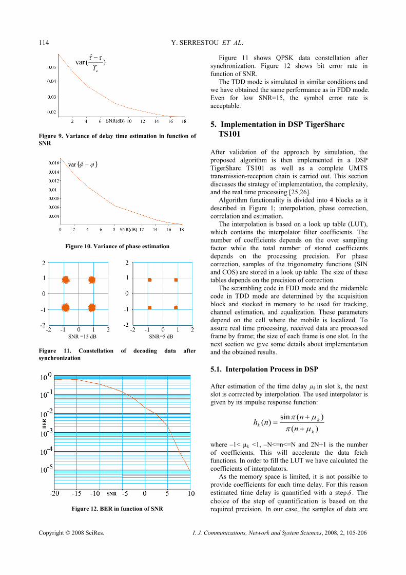
Figure 9. Variance of delay time estimation in function of SNR
Figure 10. Variance of phase estimation
SNR =15 dB SNR=5 dB
Figure 11. Constellation of decoding data after synchronization
Figure 12. BER in function of SNR
Figure 11 shows QPSK data constellation after synchronization. Figure 12 shows bit error rate in function of SNR.
The TDD mode is simulated in similar conditions and we have obtained the same performance as in FDD mode. Even for low SNR=15, the symbol error rate is acceptable. 5. Implementation in DSP TigerSharc
TS101 After validation of the approach by simulation, the proposed algorithm is then implemented in a DSP TigerSharc TS101 as well as a complete UMTS transmission-reception chain is carried out. This section discusses the strategy of implementation, the complexity, and the real time processing [25,26].
Algorithm functionality is divided into 4 blocks as it described in Figure 1; interpolation, phase correction, correlation and estimation.
The interpolation is based on a look up table (LUT), which contains the interpolator filter coefficients. The number of coefficients depends on the over sampling factor while the total number of stored coefficients depends on the processing precision. For phase correction, samples of the trigonometry functions (SIN and COS) are stored in a look up table. The size of these tables depends on the precision of correction.
The scrambling code in FDD mode and the midamble code in TDD mode are determined by the acquisition block and stocked in memory to be used for tracking, channel estimation, and equalization. These parameters depend on the cell where the mobile is localized. To assure real time processing, received data are processed frame by frame; the size of each frame is one slot. In the next section we give some details about implementation and the obtained results. 5.1. Interpolation Process in DSP After estimation of the time delay µk in slot k, the next slot is corrected by interpolation. The used interpolator is given by its impulse response function:
)()(sin
)(k
kk n
nnh
µπµπ
++
=
where –1< µk <1, –N<=n<=N and 2N+1 is the number of coefficients. This will accelerate the data fetch functions. In order to fill the LUT we have calculated the coefficients of interpolators.
As the memory space is limited, it is not possible to provide coefficients for each time delay. For this reason estimated time delay is quantified with a stepδ . The choice of the step of quantification is based on the required precision. In our case, the samples of data are

NOVEL JOINT CHIP SAMPLING AND PHASE SYNCHRONIZATION 115 ALGORITHM FOR MULTISTANDARD UMTS SYSTEMS
Copyright © 2008 SciRes. I. J. Communications, Network and System Sciences, 2008, 2, 105-206
coded with 12 bits. So the step size must be more than 2-11. Let
kµ denotes the quantification value of µk so we have:
2)1(,11, δδµδµδµµ +=⇒+<<∃−<<−∀ mmmm kkkk
Then the impulse response function of the interpolator k can be written as:
)2
(
)2
(sin)(
δδπ
δδπ
++
++=
mn
mnnhk
The data are coded with fixed point with fractional format (Q12: 12 bits are used). So it is not useful to choose precision for quantification of time delay more than the precision used in data, because the time delay is estimated by correlation of this data. So that time delay can be quantified with a step of δ = 10-7. The LUT for interpolation is organized as described in Figure 13. The size of this table is:
( )δ212 += NS
where 2N+1 is the number of interpolation coefficients, this number depends on the oversampling factor (OSF). For OSF=2 we need 5 coefficients to assure good precision and for OSF=4 or 8 we use only 3 coefficients. The number of coefficients corresponds to the number of samples used to extract the correct sample.
Figure 13. Interpolation coefficients LUT 5.2. Phase Correction & Processing in DSP To store samples of trigonometric functions, complex number representation is used, and the phase is
quantified with a step of:
512πδ =
The following table shows the arranged functions in the DSP memory:
Figure 14. Trigonometric functions LUT
The size of this table is 1024 words of 16 bits. SIN and COS tables are stored in the same 32-bit word, where the SIN samples are stocked in the more signified 16-bit (MSB) and COS samples in the last significant 16-bit (LSB). This method allows the DSP to fetch and execute complex multiplication in one clock cycle. So we get benefit from the wide memory DSP structure.
5.3. Complexity of Tracking Algorithm
We have evaluated the number of cycles required for every function and the total number of cycles required for tracking. The criterion is to assure real time. We start by giving all parameters, so we process slot by slot. The time duration of one slot is Tslot=666.667 µs. the DSP clock period is Tcycle=4 ns. We detail here the required number of cycles, which depends on the mode used (TDD or FDD) and the over sampling factor. Table 1 shows that for all values of OSF and for both modes, the processing in real time is assured. The functions that need an important number of cycles are interpolation and correlation.
5.4. Implementation Results
For the same simulation conditions, the algorithm is evaluated in a real experimental platform. The obtained results demonstrate the efficiency of the proposed tracking algorithm. For a signal to noise ratio SNR=5dB the symbol error rate is lower than 0.1%.

116 Y. SERRESTOU ET AL.
Copyright © 2008 SciRes. I. J. Communications, Network and System Sciences, 2008, 2, 105-206
Table 1. Implementation complexity
Interpolation Phase correction Correlation Estimation Total cycles Time OSF=2 51420 cycles 10480 cycles 31030 cycles 147 cycles 93077 cycles 372.31 µs OSF=4 51460 cycles 20740 cycles 31030 cycles 169 cycles 103399 cycles 413.60 µs
FDD mode
OSF=8 102620 cycles 41140 cycles 15660 cycles 169 cycles 159589 cycles 638.36 µs OSF=2 51224 cycles 10265 cycles 618 cycles 132 cycles 67807 cycles 271.23 µs OSF=4 51226 cycles 20505 cycles 15390 cycles 132 cycles 87253 cycles 349.01 µs
TDD mode
OSF=8 102450 cycles 41010 cycles 15390 cycles 132 cycles 158982 cycles 635.93 µS
Figure 15. Real and imaginary part of CPICH after synchronization for SNR= 5 dB and 15 dB
Figure 16. CPICH constellation after synchronization

NOVEL JOINT CHIP SAMPLING AND PHASE SYNCHRONIZATION 117 ALGORITHM FOR MULTISTANDARD UMTS SYSTEMS
Copyright © 2008 SciRes. I. J. Communications, Network and System Sciences, 2008, 2, 105-206
Figure 17. Constellation of decoded data after synchronization for SNR=5dB and 15dB
For this algorithm, the acquisition step is required only at the beginning of the transmission, or when the system is out-off synchronization. When the acquisition is achieved with the required precision at the beginning, tracking algorithm maintains continuously the synchronization of the received signal. This synchronization is maintained even under critical propagation conditions. Experiments shows that for time drift of 100ppm, i.e. of 10-4 Te of drift per sample duration, and phase drift of 194rad/s and at SNR = 5dB, tracking algorithm maintains synchronization and corrects the received signal with a high precision, so the BER is lower than 0.1%. In addition, during simulation we have considered just the case of propagation channel with single path, but in experimentation the multipath channel were taken into consideration. So this algorithm tracks the principal path, which has the higher power at reception. The implementation allows to change configuration, so we can change the mode (FDD or TDD) as well as the over sampling factor (OSF) without loss of synchronization. 6. Conclusions In this paper, digital joint chip timing and phase tracking for reconfigurable standard UMTS was introduced. The mathematical model of this digital tracking algorithm has been presented and used to determine the optimal parameters for implementation. The algorithm was validated by simulation and implemented in 16-bit fixed point TigerSharc DSP. Simulation was carried out in many configurations in order to confirm theoretical parameters and to evaluate the performances and robustness of this algorithm. Experiences demonstrate the feasibility of real implementation within
reconfigurable UMTS communication receiver. It shows high performance and ability to assure real time constraints and reconfiguration ability. We note that this algorithm can be adapted for other applications that use different techniques for multiple access schemes, such as chaotic communication systems. We think that our algorithm can be easily adapted for such application, and can show more performance in terms of bit error rate.
Our future work will be focalised on joint synchronization for MIMO systems. 7. References [1] R. Prasad and T. Ojanperä, “An overview of CDMA
evolution toward wideband CDMA,” IEEE Commun. Lett, vol. 1, no. 1, pp. 2–29, January 1998.
[2] T. Samanchuen and S. Tantaratana, “symbol synchronization for MC-CDMA using timing estimator and delay locked loop,” Proceeding of IEEE/ ISCIT’2005, pp. 366–369.
[3] L. Tomba and W.A. Krzymien, “Sensitivity of the MCCDMA Access Scheme to Carrier Phase Noise and Frequency Offset,” IEEE Trans. Veh. Technol., vol. 48, no.5, pp. 1657–1665, September 1999.
[4] R.A. Iltis, “A DS-CDMA tracking mode receiver with joint channel/delay estimation and MMSE detection,” IEEE Trans. Communications, vol. 49, no. 10, pp. 1770–1779, 2001.
[5] M. Latva-aho and J. Lilleberg, “Parallel interference cancellation based delay tracker for CDMA receivers,” in Proceeding of the 30th Conference on Information Sciences and Systems.
[6] W. Zha and S.D. Blostein, “Multiuser Delay-Tracking CDMA Receiver,” EURASIP Journal on Applied Signal Processing, pp. 1355–1364, December 2002.
[7] B. Jovic et al., “A robust sequence synchronization unit

118 Y. SERRESTOU ET AL.
Copyright © 2008 SciRes. I. J. Communications, Network and System Sciences, 2008, 2, 105-206
for multi-user DS-CDMA chaos-based communication systems,” in Signal Processing, vol. 87, pp. 1692–1708, 2007.
[8] R.L. Peterson, R.E. Ziemer, and D.E. Borth, “Introduction to Spread Spectrum Communications,” Prentice Hall, Inc., New Jersey, pp. 149–318 (Chapters 4 and 5), 1995.
[9] R.E. Ziemer and R.L. Peterson, “Introduction to Digital Communication,” second edition, Prentice Hall, Inc., New Jersey, pp. 611–615 (Chapter 9), 2001.
[10] J.S. Lee and L.E. Miller, “CDMA Systems Engineering Handbook,” Artech House Publishers, Boston, pp. 774–837 (Chapter 7), 1998.
[11] S. Parkvall, E.G. Ström, and B. Ottersten, “The impact of timing errors on the performance of linear DS-CDMA receivers,” IEEE Journal on Selected Areas in Communications, vol. 14, no. 8, pp. 1660–1668, 1996.
[12] J.C. Lin, “Low-complexity code tracking loop with chip-level differential detection for DS/SS receivers,” IEEE Electronic Letters, vol. 36, no. 24, 23rd November 2000.
[13] E. G. Strom, S. Parkvall, S. L. Miller, and B. Ottersten, “Propagation delay estimation in asynchronous direct-sequence code-division multiple access systems,” IEEE Trans. Communications, vol. 44, no. 1, pp. 84–93, 1996.
[14] Y. Serrestou, K. Raoof, J. Liénard, “Digital joint sampling instant and phase synchronization for UMTS standard,” IEEE/ACES International Conference on Wireless Communications and Applied Computational Electromagnetics PN: 905565, Hawaii, 2005.
[15] F.M. Gardner, “Interpolation in digital Modems,” IEEE Trans. on comm., vol.41, no.3, March 1999.
[16] 3GPP TS 25.211, “Physical layer-General description,” Technical Specifications of the 3rd Generation Partnership Project. http://www.3gpp.org/ftp/Specs
[17] 3GPP TS 25.211, “Physical channels and mapping of transport channels onto physical channel FDD,”
Technical Specifications of the 3rd Generation Partnership Project. http://www.3gpp.org/ftp/Specs
[18] 3GPP TS 25.212, “Multiplexing and channel coding FDD,” Technical Specifications of the 3rd Generation Partnership Project. http://www.3gpp.org/ftp/Specs
[19] 3GPP TS 25.221, “Physical channels and mapping of transport channels onto physical channel TDD,” Technical Specifications of the 3rd Generation Partnership Project. http://www.3gpp.org/ftp/Specs
[20] 3GPP TS 25.222, “Multiplexing and channel coding TDD,” Technical Specifications of the 3rd Generation Partnership Project. http://www.3gpp.org/ftp/Specs
[21] L. Krikidis, J.L. Danger, and L. Naviner, “A DS-CDMA multi-stage inter-path interference canceller for high bit rates,” 2004 IEEE Eighth International Symposium on Spread Spectrum Techniques and Applications, pp. 405–408, August 30 – September 2, 2004.
[22] L. Krikidis, J.L. Danger, and L. Naviner, “Flexible and reconfigurable receiver architecture for WCDMA systems with low spreading factors,” Electronics Letters, vol. 41, no. 1, pp 22–24, January 6, 2005.
[23] F.M. Gardner, “Interpolation in digital Modems,” IEEE Trans. on comm., vol. 41, no. 3, March 1999.
[24] R.E. Crochiere, “Optimum FIR digital filter implementations for decimation, interpolation, and narrow-band filtering,” IEEE Trans. on acoustics speech and signal processing, vol. ASSP-23, no. 5, October 1975.
[25] A. Devices, “Tuning C source code for the TigerSharc DSP compiler,” Engineer to engineer note, EE-147, January 2001.
[26] A. Devices, “16-bit FIR filters ADSP-TS20x TigerSharc processors,” Engineer to engineer note, EE-211, January 2004.