novel materials and packaging for thermoelectric waste-heat
TRANSCRIPT

Novel Materials and Packaging for Thermoelectric Waste-Heat Recovery in Building and Transportation Systems
Final Technical Report
Kenneth E. Goodson
Mechanical Engineering Department Stanford University
Stanford, CA 94305-3030
Executive Summary Thermoelectric recovery is promising for improved efficiency in a broad variety of combustion systems, but thermal interface resistances and the need for scalable and package-compatible thermoelectric materials is a major roadblock. We report progress on six different activities this year, which are all in support of the major goal of novel materials for thermoelectric waste-heat recovery: 1) Thermal interface resistance measurements for the growth interface, using through-wafer picosecond thermoreflectance. 2) Thermal interface resistance of films in contact with a variety of top-side metallizations (Ti, Ni, Al, Pd, Cr), including both the engagement factor of the nanotubes with the coating and the effective thermal contact resistance. 3) Total resistance measurements of CNT films considering varying CNT density and length and inclusion of polymer matrix. 4) CNT deposition on thermoelectric materials including SiGe and characterization of the resulting thermal properties. 5) Elastic modulus measurements captured using resonant frequency experiments on microfabricated cantilever structures and laser interferometry. 6) A sub-contract with the Wardle group at MIT yielding indentation-based measurements of the elastic modulus.
1. Introduction The imbalance of research on thermoelectric systems has grown both more prominent and more problematic for the development of this technology. The overwhelming majority of research funding is directed to the thermoelectric efficiency of the basic constituent thermoelectric materials with very little consideration of packaging a practical device; the surrounding interfaces and packaging can drastically change efficiency at the system level. Recent industry and research outcomes underscore the need for combining fundamental material development with practical, system-level considerations. For instance, the potential efficiency improvements resulting from nanostructured materials were lauded and gave rise to multiple studies which characterized thermoelectric properties of individual nanowires [1]. Films or large arrays of nanowires are more realistic thermoelectric generator (TEG) material options, and there is evidence that arrays have unique characteristics which are not present in studies on individual nanotubes or wires [2]. Nonetheless, few nanowire films have been characterized, leaving end-users without the efficiency gains proposed by theorists. Within the last year alone, several groups have created TEGs with novel thermoelectric materials only to find that interfaces between the thermoelectric materials and other system components are the foremost limitation to thermoelectric conversion efficiency [3]. Wide temperature fluctuations, prolonged thermal cycling, and large contact area in thermoelectric systems both degrade the performance of traditional interface materials and make the TEG more susceptible to device failure from thermal expansion

mismatch. Several groups report device breakage while others add flexible expansion strips which then reduce device performance [4]. The need for interface materials with high thermal conductivity and mechanical compliance is becoming increasingly urgent in TEG systems [5]. Nanostructured thermal interfaces composed of carbon nanotubes (CNTs) may perform as an exceptional thermal interface material, but further thermal and mechanical characterization of CNT arrays is required. Owing to their outstanding thermal properties, aligned arrays of carbon nanotubes (CNTs) are promising for use in advanced composites and interfaces requiring high thermal performance and mechanical compliance. In spite of the high conductivity of individual carbon nanotubes, the interface resistance of the CNT-substrate contacts often significantly reduces the thermal performance of CNT films and their composites below its potential value [6-8]. The complicated structure of these interfaces at the nanoscale strongly affects the interface resistances and is highly dependent on the interaction, adhesion, and wettability of the CNT and substrate materials, which is typically a metallic layer or dielectric. The nanoscale features in the contact further complicate the interface resistance by modifying the phonon transport physics, for which there are no established models. Further data are needed for the interface resistance between CNT interfaces with metal and dielectric films and its temperature dependence to improve upon the thermal performance of CNT arrays and develop models for the thermal transport in nanostructured contacts. We utilize a comprehensive set of thermal and mechanical characterization tools to measure the impact of CNT density, length, and surrounding matrix on the thermal and mechanical properties as a function of temperature from -40 to 400ºC. In the past few years, some attention has been given to the toxicity and scarcity of the common thermoelectric materials. However, the significance of these factors is largely ignored by many groups who are developing new thermoelectric materials which are often made with these toxic and scarce materials. Moreover, the growing field of solar photovoltaic generation is increasing the demand for some of the same key materials used in thermoelectrics. A critical benefit of nanostructured thermoelectric materials lies in their increased efficiency combined with the use of cheaper, non-toxic materials. Additionally, people are only recently considering the reality that specific niche markets are appropriate for thermoelectric power generations [9]. TEGs should be developed from the outset for these specific markets, and the key markets are in waste heat recovery in building and transportation systems (e.g. building appliances, heating sytems, and automotive exhaust systems). After exploring the field extensively and having a helpful discussion with Prof. Jim Sweeney, we realize that we may be the sole group to explore the interconnection between all aspects of this technology from raw materials to system-level integration. Considerations such as material supply, material cost, current state-of-the-art, fabrication cost, competing influences from other applications, and market applicability require a holistic approach that we are uniquely capable of providing. In the next sections, we address and report progress on the following challenges:
1. The lack of interface materials that yield satisfactory system efficiency and reliability. 2. The need for novel thermoelectric materials that combine optimal properties to
demonstrate high efficiency. 3. The dearth of viability assessments for thermoelectric technology.
2. Carbon nanotube array thermal interface materials
2.1 CNT-Growth Substrate Thermal Contact Resistance The importance and physics of the thermal resistance at the CNT-growth substrate interface is currently poorly understood, with previous measurements of this value spanning a large range of 0.022- 50
mm2K/W [10, 11]. Furthermore, since the nanoscale geometry of the growth interface is more definable than that at the CNT tips, the thermal characterization of this interface can provide insight into fundamental phonon transport between low dimensional nanostructures and semi-infinite media. Measurements that accurately isolate this interface resistance are challenged by need of achieving deep sub-micron heating confinement near the buried interface. We have developed first-of-kind picosecond Time Domain Thermoreflectance (TDTR) measurements of the growth interface for CNTs grown on metal-coated transparent substrates, which provide optical access to the metallic film in close proximity to the CNT interface. Picosecond TDTR is a well-established technique [12] that measures the cross-plane distribution of thermal properties with deep sub-micron spatial resolution by heating the metallic film through the transparent substrate using 10 ps pulses from a modelocked Nd:YVO4 laser. The reflected intensity of a variably delayed co-aligned probe beam derived from the pump beam measures the relative temperature change of the metal film, which is fit to a rigorous solution of the heat diffusion equation for a multi-layer stack to extract the MWNT base interface resistance. Figure 1 shows a schematic of the TDTR system in the Stanford Micro/Nano Scale Heat Transfer Laboratory.
Figure 1: Schematic of the picosecond pump-probe optical metrology platform. The system uses a variable delay stage to control the relative delay time between modulated pump (red path) and probe pulses (blue path) to achieve temporal resolutions down to 10 ps.
Figure 2: TEM illustrating the successful growth on Al2O3/W/SiO2 substrate for measurements of the thermal interface resistance between the MWNT and substrate.
The TEM image in Figure 2 shows our recent achievement of the successful growth of MWNTs (~10 nm diameter) on a thin-film multilayer stack consisting of Al2O3 (32 nm) and W (34 nm) on a SiO2 substrate. We are currently in the progress of performing measurement of the thermal interface resistance in the range of 70-300 K. Currently, the lowest temperature that we can achieve (~70 K) is limited by the low thermal conductivity substrate (SiO2) creating significant steady-state heating from the lasers. To achieve lower temperatures (~10 K), we are currently in the process of developing the MWNT growth on metalized sapphire substrates coated with a thin (~500 nm) SiO2 film. The higher conductivity of this substrate reduces the steady state heating below 5 K while the thin oxide layer provides a high thermal resistance for sub-nanosecond thermal diffusion, which forces heat into the CNT film and increases the sensitivity to the thermal interface resistance. We are also amplifying the sensitivity to the interface resistance by developing a successful CNT growth process for thinner Al2O3 films directly on the metallic film.
1064 nm probe532 nm pump1064 nm pump
1064 nm probe532 nm pump1064 nm pump
1064 nm probe532 nm pump1064 nm pump
1064 nm probe532 nm pump1064 nm pump
MWNT
Al2O3
W
SiO250 nm
MWNT
Al2O3
W
SiO250 nm

2.2 CNT-Metallization Thermal Contact Resistance In many thermal applications the aligned CNT films are interfaced with a substrate using thin metallic films (adhesion layers and solders). The effective thermal resistance of the CNT thermal interface is often limited by this contact resistance, which is strongly determined by the metal-CNT interactions and its structure at the nanoscale [6]. This program provides comprehensive thermal data using nanosecond thermoreflectance thermometry for the thermal properties, including first-of-kind temperature dependence, of SWNT films grown on Si coated with various metals. The nanosecond thermoreflectance technique, which has been applied to the measurement of the thermal properties of metal-coated SWNT arrays in our previous work [6], uses 6 ns pulses from a Nd:YAG laser to heat the surface of the metal film. The reflected intensity of a CW probe laser is collected by a fast photo diode and oscilloscope (650 MHz bandwidth) and measures the metal surface temperature. The SWNT films are grown using alcohol catalytic CVD to a length of 11.5 um and densities of 3% using a Co-Ni catalyst deposited on a Si substrate. Fifty nanometers of either Al, Pd, Ni, Ti, or Cr is evaporated on separate SWNT samples. Fabricating samples out of the same SWNT reduces variations in the thermal property data caused by variations in SWNT quality, volume fraction, and length. Fitting the nanosecond thermoreflectance data with the solution of the heat diffusion equation for the multilayer stack extracts the SWNT-metal interface resistance, the SWNT-substrate interface resistance, and the effective heat capacity of the SWNT film. Since the volumetric resistance due to the effective thermal conductivity of the SWNT film is much less than that from the interface, the data extraction is insensitive to the effective SWNT conductivity, yielding only a lower bound of ~1 W/m/K. Dividing the measured effective volumetric heat capacity by that of an individual SWNT provides a good approximation for the effective volume fraction, feff=Cv,eff/Cv,indiv cnt, of SWNTs participating in heat transfer [6]. Since the individually coated samples originated from the same growth, an increasing effective volume fraction indicates improve metal-SWNT interaction and thermal contact. Figure 3(a) shows the effective metal-SWNT, SWNT-substrate, and total interface resistance as a function of the extracted feff for the set of metallizations. Figure 3(b) shows the temperature dependence of the effective interface resistances and heat capacity of the Al-coated SWNT film. The results indicate that the Ti interface provides the best contact with the lowest thermal resistance. The resistance dependence on the metal schedule and the trend of decreasing interface resistance with increasing feff is in qualitative agreement with observations of relative coating ability of the various metals with SWNTs observed in other work [13]. These results support the importance of metal-SWNT interactions in improving the thermal performance of the CNT arrays.
Figure 3: (a) Thermal interface resistance data for metalized SWNT arrays as a function of extracted effective volume fraction. (b) Temperature dependence of the thermal interface resistance and effective heat volumetric heat capacity of the Al-coated SWNT film (samples provide by the Wardle Group at MIT and the Maruyama Group at University of Tokyo).
0
10
20
30
40
50
0 0.005 0.01 0.015 0.02
R metal-SWNT
R SWNT-Substrate
R total
feff=Cv,eff/Cv,individual
Inte
rfac
e R
esis
tanc
e (m
m2 K
/W)
Al Pd NiTi
Cr
0
10
20
30
40
50
0 0.005 0.01 0.015 0.02
R metal-SWNT
R SWNT-Substrate
R total
feff=Cv,eff/Cv,individual
Inte
rfac
e R
esis
tanc
e (m
m2 K
/W)
0
10
20
30
40
50
0 0.005 0.01 0.015 0.02
R metal-SWNT
R SWNT-Substrate
R total
feff=Cv,eff/Cv,individual
Inte
rfac
e R
esis
tanc
e (m
m2 K
/W)
Al Pd NiTi
Cr
020406080
100120140
0 100 200 300
Rcnt-metalCeff cntRsub
Inte
rfac
e R
esis
tanc
e (m
m2 K
/W)
or H
eat C
apac
ity (J
/m3 /K
)
Temperature (K)
020406080
100120140
0 100 200 300
Rcnt-metalCeff cntRsub
Inte
rfac
e R
esis
tanc
e (m
m2 K
/W)
or H
eat C
apac
ity (J
/m3 /K
)
Temperature (K)
a) b)

2.3 CNT Deposition and Characterization on Thermoelectric Materials
Temperature drops at the interfaces between thermoelectric materials and the heat source and sink reduce the overall efficiency of thermoelectric systems. Nanostructured interfaces based on aligned carbon nanotubes promise the combination of mechanical compliance and high thermal conductance required for thermoelectric modules, which are subjected to severe thermomechanical stresses. Previous work has shown that nanostructured interface materials based on carbon nanotubes (CNTs) can minimize thermomechanical stresses for microprocessor applications [6]. However, the challenge of extending nanostructured interfaces to thermoelectric applications with larger temperature differences and different material combinations has not been addressed. Our work extends mechanical and thermal requirements of interfaces, based on microprocessor operating conditions, to conditions in thermoelectric generation systems. We demonstrate growth of aligned multiwalled CNT films on a candidate thermoelectric material and measure the thermal properties associated with the CNT interface material. Thermal property data for 1.5 μm, 2.5 μm, and 70 μm thick CNT films on SiGe were taken using the same nanosecond thermoreflectance technique detailed in the previous section. SiGe was chosen because of its ability to withstand CNT growth temperatures of over 800ºC. Figure 3(a) shows a schematic of the samples used in our measurements, including the locations of the measured boundary resistances and SEM images of the as-grown CNT array. Table 1 shows the results for the three samples. These values are comparable to those of previous work on multiwall CNT arrays, which have total resistances from 0.8 m2 K MW-1 to 61 m2 K MW-1 [10, 14]. The boundary resistances dominate thermal decay in the thinner two samples. For the 70 μm film, we cannot extract thermal conductivity separately from the lower boundary resistance, so we can only determine the total resistance through the film. A thermal resistance of 3.3 m2 K MW-1 is comparable to a typical 40 μm layer of thermal grease. The high thermal resistances at the film boundaries indicates that a low number of tubes make good thermal contact to the surrounding substrate and metal, as reflected in the low feff of the CNT array. The 2.5 μm and 70 μm film may be performing better due to better growth quality (increased density and contacts at tube ends). In practical applications of the CNT film, the boundary resistances may be reduced with the use of a binder material to conform to the rough CNT surface and make good thermal contact with more tubes [6]. The effect of 100 thermal cycles from 30°C to 200°C was also studied for the 1.5 μm thick CNT film using an INSTEC® temperature controlled stage (Figure 4). These data provide the groundwork for future studies of thermoelectric materials in contact with CNT films serving as both a thermal and electrical interface.
3.6 μm SiGe & Si/Ge Superlattice
Si Substrate
Heat Flux
R”CNT-Metal
20nm Al2O3 /1nm Fe
CNT Array
50 nm Al/20nm Pd
R”CNT-Base
20 μm 1 μm
(a) (b) (c)
Figure 4: (a) Schematic of sample geometry. A CNT array is grown on a layered SiGe and Si/Ge superlattice substrate. A metal layer is deposited on the CNT array for thermoreflectance thermometry, in which heat flux is

applied to the metal; (b) & (c) SEM image of 70 μm (b) and 2.5 μm (c) CNT film grown on SiGe / Si substrates, after metallization.
Table 1. Results for CNT array grown on SiGe substrate Average Result Uncertainty
1.5 μm CNTs R”CNT-Metal R”CNT-Sub
Cv, eff feff
13 m2 K MW-1
34 m2 K MW-1 8.2 kJ m-3 K-1
0.9%
30 40 50
2.5 μm CNTs R”CNT-Metal R”CNT-Sub
Cv, eff feff
1.4 m2 K MW-1
1.8 m2 K MW-1 11.6 kJ m-3 K-1
1.6%
10 40 50
70 μm CNTs R”CNT-Pt R”Total Cv, eff feff
1.3 m2 K MW-1
3.3 m2 K MW-1 10.7 kJ m-3 K-1
0.33-1.8%
10 40 70
Figure 5: Effect of thermal cycling from 30°C to 200°C on CNT film boundary resistances.
2.4 Impact of Density in MWCNT Films and Nanocomposites Experimental measurements of the thermal conductivity of individual nanotubes have shown values ranging from 500 to 3200 W/(m K) [15, 16]. Arrays of vertically aligned CNTs can potentially take advantage of the high axial thermal conductivity, but they are limited in part by a low packing fraction of CNTs in the array and the interface resistance at the CNT-substrate contacts. A simple model of the aligned CNT arrays as conductors in parallel suggests that thermal conductivity should scale with the packing fraction of CNTs. Aligned-carbon nanotube (CNT) forests (A-CNTs) and aligned CNT polymer nanocomposites (A-PNCs) form the basis for uniquely-well-controlled nano-scale morphologies, creating specimens whose thermophysical properties are able to be interpreted relative to models. These materials are fabricated by chemical vapor deposition of multi-wall carbon nanotubes (previously characterized to have 8 nm diameter with ~3-7 walls ) , biaxial mechanical densification (to achieve variable and controlled volume fraction Vf, see Figure 6), and capillary-driven infiltration with a high-performance thermoset (aerospace

grade structural epoxy, RTM6) for A-PNCs2. The A-PNCs morphologies were evaluated using scanning-electron microscopy (SEM), for CNT alignment within the polymer. The aerospace-grade resin (Hexcel RTM6) shows a relatively smooth surface whereas samples with A-PNCs have a surface morphology indicating both CNT alignment and packing. Increasing the volume fraction of the aligned CNTs from 1% to 20% alters the fracture surface significantly and also serves as a visual indication of alignment and effective wetting (Figure 7). Small and wide-angle x-ray scattering (SAXS and WAXS) have also confirmed this morphology. Thermal characterization of A-CNTs and A-PNCs is undertaken by measuring temperature gradient using infrared (IR) microscopy (Figure 8). Thermal dissipation and scattering are large error sources in the thermal measurement, but thermal resistance evaluation at thermal contacts is straightforward with this technique. Currently, thermal conductivities are measured along the CNT direction. As shown in Figure 8b, the CNT length showed little effect on effective thermal conductivities of A-CNTs, possibly because their length (~100s of µm) are much larger than the phonon mean free path at room temperature (~1 µm), resulting in the diffusive transport regime. On the other hand, as shown in Figure 8c, CNT Vf has also shown little effect on effective thermal conductivity of A-CNTs and A-PNCs, possibly because of thermal conduction in the across-CNT directions through inter-CNT contacts. Meanwhile, slight conduction suppression has been observed by embedding CNTs in polymer. Further study with enhanced thermal contacts and measurement in the across-CNT directions are planned for better understanding of thermal transport in A-PNCs. Models are being applied to help interpret the new data, incorporating relevant aspects of the A-CNT and A-PNC morphologies.

(a)
(b)
Figure 6: Fabrication of variable volume fraction aligned-CNT nanocomposites: a) fabrication process flow of A-PNCs, and b) scanning electron microscopy images of maintained CNT alignment before (~1% Vf) and after (~20% Vf) mechanical densification.
Figure 7: SEMs of (a) Epoxy sample, (b) 1% Aligned-PNC, (c) 20% Aligned-PNC. In images (b) and (c), the direction of CNT alignment is indicated.

Figure 8: Thermal conductivity measurement of A-CNTs and A-PNCs: a) IR detector setup schematics and temperature gradient map example, b) effective thermal conductivity of A-CNTs with CNT length as the parameter, and c) effective thermal conductivity of A-CNTs and A-PNCs with CNT Vf as the parameter.
(a)
(b)
(c)
0
0.2
0.4
0.6
0.8
1
1.2
1.4
0 200 400 600 800 1000 1200
L (um)
k (W
/m/K
)C
NT
fore
st th
erm
al
cond
uctiv
ity [W
/m.K
]
0
0.2
0.4
0.6
0.8
1
1.2
1.4
0 200 400 600 800 1000 1200
L (um)
k (W
/m/K
)C
NT
fore
st th
erm
al
cond
uctiv
ity [W
/m.K
]
0
1
2
3
4
0 5 10 15 20 25CNT Volume Fraction [%]
Eff
ectiv
e A
ligne
d-C
NT
Fore
st/C
ompo
Th
erm
al C
ondu
ctiv
ity [W
/m/K
]
Densified CNTs
PNCs

2.5 Mechanical Characterization using Resonators One method we are investigating for characterizing the mechanical properties of CNT arrays in parallel with measuring the thermal properties involves depositing the CNT film directly on microresonators. The CNT film shifts the resonant frequency of the microresonator (compared to a resonator without coating). The shift in resonant frequency allows for determination of mechanical properties of the thin film coating the cantilever [17]. Using Laser Doppler Velocimetry (LDV) to compare the resonant frequency of identical cantilevers with various thicknesses of CNT layers, mechanical properties such as lateral Young’s modulus, nanotube packing density, and potentially thermo-mechanical dissipation mechanisms can be extracted. To measure all unknown mechanical properties, multiple resonator geometries must be designed and fabricated emphasizing different properties. Figure 9 illustrates the concept for integrating the mechanical and thermal samples into the same wafer to provide a novel technique for measuring the mechanical and thermal properties in parallel on identical samples. Optimization of the CNT growth process through comprehensive experimental trials varying CNT growth parameters led to a growth process that is compatible with the MEMS resonator fabrication and gives dense nanotube films. A first round of fabrication and growth of dense aligned multiwalled nanotube films on the resonator structure has been developed successfully as shown by the cantilever coated with a CNT film in Figure 9. Currently, we are building a rigorous finite element thermo-mechanical model for extracting the mechanical properties from LDV data. A second round of cantilever fabrication using a new fabrication procedure is in progress. The new technique should yield improved cantilevers and CNT films for LDV. The process requires a cantilever fabrication using backside etching, an aluminum oxide deposition, catalyst coating, and elevated growth temperatures (850 ºC).
Figure 9: Schematic of mechanical and thermal characterization structure
Laser Doppler Velocimeter
Vibrometer, ω
Pump Probe
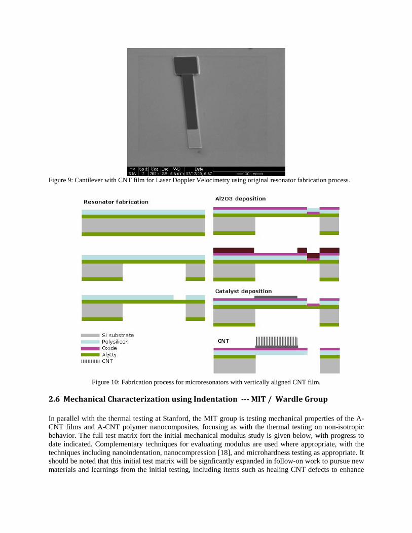
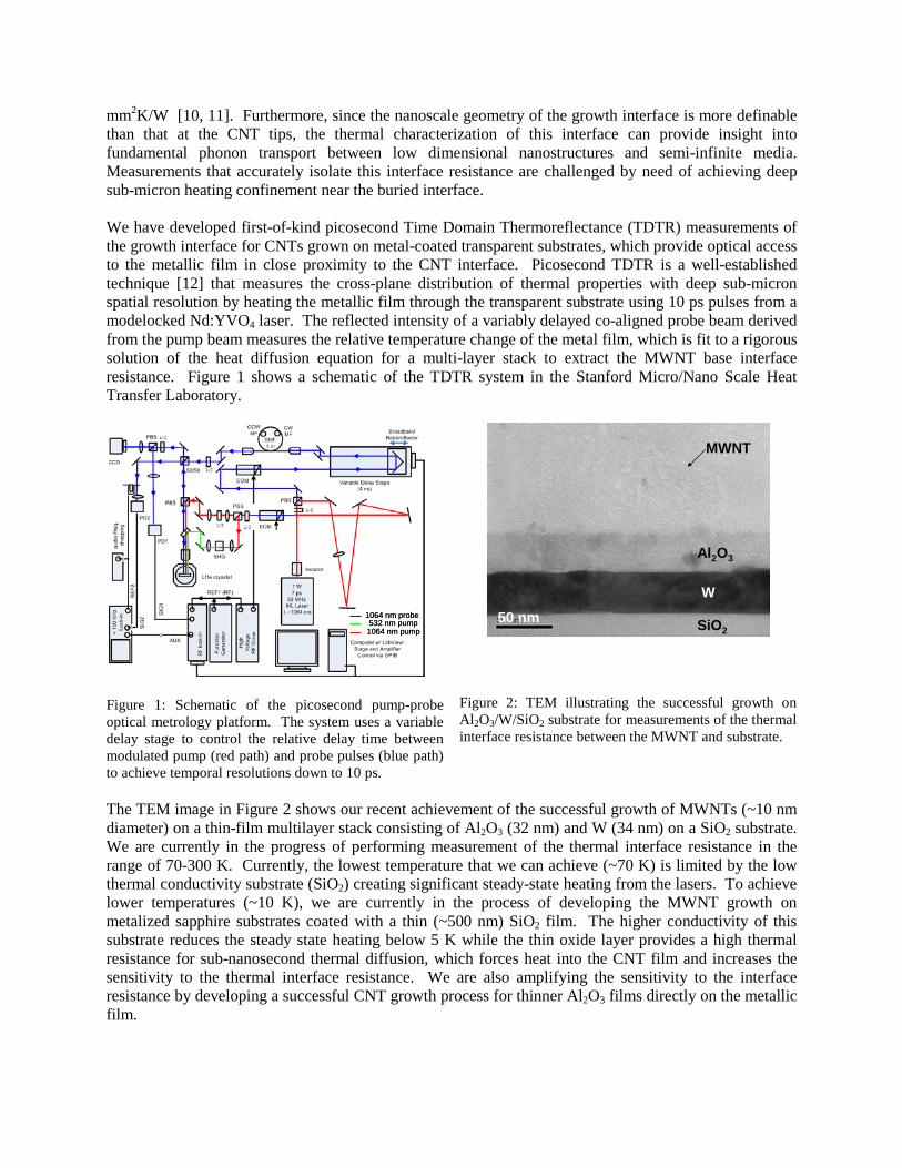
Figure 9: Cantilever with CNT film for Laser Doppler Velocimetry using original resonator fabrication process.
Figure 10: Fabrication process for microresonators with vertically aligned CNT film.
2.6 Mechanical Characterization using Indentation --- MIT / Wardle Group In parallel with the thermal testing at Stanford, the MIT group is testing mechanical properties of the A-CNT films and A-CNT polymer nanocomposites, focusing as with the thermal testing on non-isotropic behavior. The full test matrix fort the initial mechanical modulus study is given below, with progress to date indicated. Complementary techniques for evaluating modulus are used where appropriate, with the techniques including nanoindentation, nanocompression [18], and microhardness testing as appropriate. It should be noted that this initial test matrix will be signficantly expanded in follow-on work to pursue new materials and learnings from the initial testing, including items such as healing CNT defects to enhance
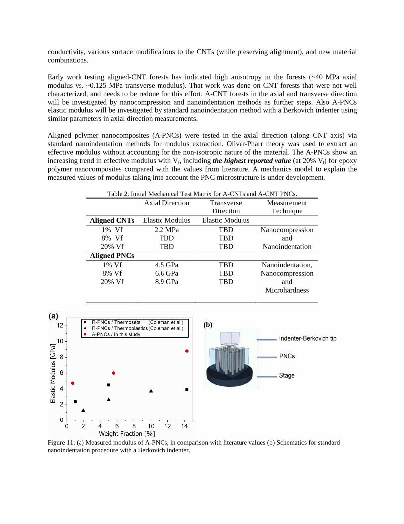
conductivity, various surface modifications to the CNTs (while preserving alignment), and new material combinations. Early work testing aligned-CNT forests has indicated high anisotropy in the forests (~40 MPa axial modulus vs. ~0.125 MPa transverse modulus). That work was done on CNT forests that were not well characterized, and needs to be redone for this effort. A-CNT forests in the axial and transverse direction will be investigated by nanocompression and nanoindentation methods as further steps. Also A-PNCs elastic modulus will be investigated by standard nanoindentation method with a Berkovich indenter using similar parameters in axial direction measurements. Aligned polymer nanocomposites (A-PNCs) were tested in the axial direction (along CNT axis) via standard nanoindentation methods for modulus extraction. Oliver-Pharr theory was used to extract an effective modulus without accounting for the non-isotropic nature of the material. The A-PNCs show an increasing trend in effective modulus with Vf, including the highest reported value (at 20% Vf) for epoxy polymer nanocomposites compared with the values from literature. A mechanics model to explain the measured values of modulus taking into account the PNC microstructure is under development.
Table 2. Initial Mechanical Test Matrix for A-CNTs and A-CNT PNCs. Axial Direction Transverse
Direction Measurement
Technique Aligned CNTs Elastic Modulus Elastic Modulus
1% Vf 8% Vf 20% Vf
2.2 MPa TBD TBD
TBD TBD TBD
Nanocompression and
Nanoindentation Aligned PNCs
1% Vf 8% Vf
20% Vf
4.5 GPa 6.6 GPa 8.9 GPa
TBD TBD TBD
Nanoindentation, Nanocompression
and Microhardness
(b)
Figure 11: (a) Measured modulus of A-PNCs, in comparison with literature values (b) Schematics for standard nanoindentation procedure with a Berkovich indenter.

3. Novel Thermoelectric Generator Materials 3.1 Aligned nanowire arrays During the past year, we have been partnering with Prof. Xaolin Zheng’s group in the Mechanical Engineering department. Prof. Zheng’s group fabricates aligned silicon nanowire arrays with a wet etch process that allows excellent control over nanowire length and height uniformity (Figure 12). Through the partnership, Prof. Zheng’s group is varying aspects of the nanowire arrays such as doping, length, and diameter, and our group characterizes the thermoelectric property dependence on these parameters.
Figure 12: a) Densely-packed aligned silicon nanowire array. b) Polymer-filled nanowire array to provide smooth contact surface (J. Weisse, Zheng group).
(a) (b) 3.2 Randomly-oriented nanowire films Through the Global Climate & Energy Project seminars, the we learned of the materials synthesis work of Prof. Alberto Salleo’s group in the Materials Science and Engineering department. The Salleo group fabricates nanostructured zinc oxide films (Figure 13) for transparent conductor applications [19]. We recognized the ZnO film’s potential for high thermoelectric performance due to the nanoscale structures in the film which decrease thermal conductivity. This thermal conductivity reduction combined with a reasonably low electrical resistance (Figure 14) could result in an increase in the thermoelectric figure-of-merit [20]. Moreover, the ZnO nanowire solution can be deposited into uniform films through low-cost processing means such as spray coating. We are currently developing characterization techniques and sample structures tailored to the unique features of these nanowire films. Proof-of-concept studies demonstrate our ability to utilize techniques that measure both lateral and cross-plane properties. We are adapting our techniques to overcome roughness of the film surface and the film’s sensitivity to solution-based processing.

(a) (b) (c) Figure 13: a) SEM of ZnO nanowire film. b,c) AFM data of trench etched in nanowire film to determine film thickness show surface roughness of film.
(a) (b) (c) Figure 14:a) New sample structure designed to overcome surface roughness challenges in thermoreflectance measurement. b) Sample of thermoreflectance data. Uncertainty in film thickness produces large uncertainties in extracted thermal properties. c) Electrical resistance data for ZnO nanowire films obtained by 4-probe technique [19].
(a) (b) Figure 15: a) Infrared thermometry sample setup to determine cross-plane thermal properties of film. b) Infrared thermometry data showing temperature gradients in sample. The resolution of the setup does not allow for differentiation between thermal gradients in film versus metal heating layers, so the method is being evaluated for measurements of in-plane film properties.

3.3 GST thin films
Generally, special microfabricated structures must be developed in order to measure the Seebeck coefficient of thin films. We have developed a design for microfabricated electrothermal structures that will enable both in- and cross-plane Seebeck coefficient measurements. The in-plane measurements are done by establishing a 1D thermal gradient. Cross-plane measurements are accomplished through an AC heating technique, the 3ω method. The harmonic responses correspond to thermoelectric properties. Initial testing on Ge2Sb2Te5 demonstrates the ability of the structures to obtain the voltage potential that results from a temperature gradient established across and through blanket thin films. We are currently determining how to perform the same measurements on nanostructured films that cannot undergo traditional microfabrication processes.
(a) (b) (c) Figure 16: a) Top view of microfabricated structure to measure in-plane Seebeck coefficient of thin film, in this case GST. b) Cross-sectional schematic of structure to measure cross-plane Seebeck coefficient. c) Preliminary data demonstrating ability to obtain thermoelectric response of thin film. 4. Assessment of thermoelectric technology viability While there is interest in waste heat recovery using thermoelectrics, there are relatively few studies of the viability of this technology. Vining concluded there are niche markets for thermoelectric power generation for low to moderate power levels, but, beyond automotive exhaust heat recovery, he did not elaborate on specific markets [9]. We have identified potential applications in building systems, and we compare the requirements for technological advancement in thermoelectrics for both building and automotive applications. Given the proposed materials and interface improvements, the cost of thermoelectric power generation could reasonably drop from $16.5/W to $12/W [21]. Conventional wisdom has focused on improving the figure-of-merit, ZT, regardless of the type of application. However, one of the key factors for decision-making appears to be system operating temperature. In automotive applications, thermoelectrics are most promising for exhaust heat recovery where the temperatures are relatively high (about 300°C) [22]. The picture may be quite different in building systems. Naturally, we initially considered applying thermoelectrics to combustion appliances in buildings such as water heaters because of the high heat fluxes. While this is still a viable option, further research indicates that low-grade heat recovery may be the optimum application in building systems. Although thermoelectric power generation will not be higher, the impact on improved energy efficiency in buildings would be more significant.
Heater bridge
Thermometer bridge
Temperature gradientGST bridge
SiO2Pt
GSTTiN
TiN
Pt
Si
V2ω
R² = 1.000
0
5
10
15
20
25
30
35
0.000 0.005 0.010 0.015 0.020 0.025
2ωVo
ltag
e [
mV
]
Power [W]

Low-grade heat recovery from heating systems is likely the optimal application of thermoelectric power generation in buildings. Table 3 shows the breakdown of the top energy uses in residential and commercial buildings [23]. For residential buildings, space heating accounts for the largest portion of energy consumption; it is the second largest in commercial buildings. Rapid advancement of lighting technology will likely reduce energy use for commercial lighting, so space heating energy efficiency improvement will become a more pressing need. Up to 35% of the heat output of heating systems is lost in duct and piping systems [24], so heat recovery throughout the heating system, not just at the heat source, is a reasonable consideration. Moreover, thermoelectric power generation at the lower temperatures is more efficient since the materials properties are better, and the interfacial constraints are less pronounced (see Figure 17).
Table 3: Energy consumption breakdown in residential and commercial buildings. Residential Commercial Space heating 32% 16% Lights 12% 28% Water heating 13% 7% Space cooling 10% 13%
Figure 17: Thermoelectric power generation as a function of device ZT for proposed automotive (high temperature) and building (low temperature) applications. The ZT of standard and novel materials is shown. BiTe indicates the compound Bi2Te3. The novel nanostructured materials properties are from recent (the last 5-7 years) research worldwide. Achieving a ZT of 2 is a reasonable expectation. ZT of 4 will require aggressive research in both thermoelectrics and interface materials and integration. A key datapoint to determine thermoelectric viability is a comparison of the electricity production potential with the materials cost [25]. The materials cost is comprised of the cost of extraction and the processing cost. Although the manufacturing cost and quality are critical, data on these characteristics are quite elusive. In fact, Wadia, Alivisatos, and Kammen provided an already much-cited study on this analysis for solar cell materials, and they omitted the processing cost from the analysis due to the lack of data and insufficient market penetration [26]. Compared to photovoltaic industry development, thermoelectric industry experience is even more limited. We attempted to complete a similar analysis as Wadia et al., but the lack of analysis and modeling of heat recovery in building heating systems precludes such an approach [27]. Both the extraction costs and the electricity production potential necessitate such
0 0.5 1 1.5 2 2.5 3 3.5 40
0.02
0.04
0.06
0.08
0.1
0.12
0.14
0.16
ZT
Effi
cien
cy
AutomotiveBuilding
ZnO
PbTe BiTe
Si
Potential increase from nanostructuring
Potential efficiency increasesfrom improved interfaces
Novel nanostructured materials
Established materials

an analysis. However, mineral production and reserves can provide some indication of which materials to pursue, particularly in light of competing technologies (Table 4) [28].
Table 4: Availability of thermoelectric materials [28]. Mineral Production
(x1000 tons) Reserves
(x1000 tons) Competing
industry
Traditional materials
Bismuth 7.3 320 Lead 3.9 79 Tellurium N/A 22 Solar, Electronics Germanium 140 450 Electronics Selenium 1.5 88
Potential materials Silicon 5.4 Very abundant Electronics Zinc 11 200 Electronics
It is quite evident that the thermoelectrics industry must investigate other materials besides the traditional candidates of bismuth telluride, lead telluride, and silicon germanium. However, current research in the field does not reflect this need. Competing, fast-growing industries combined with materials toxicity limitations will necessitate use of materials such as the silicon and zinc films we are developing. 5. Conclusion We have addressed the most critical aspects of thermoelectric waste heat recovery in building and automotive systems. We made progress in developing a carbon nanotube array thermal interface material to improve thermoelectric device efficiency. We developed metrology techniques to characterize novel, nanostructured films made of earth-abundant materials. Finally, we determined the component of building systems that could utilize thermoelectric technology for the greatest improvement in overall building energy efficiency. The analysis identified a need for feasibility analyses about incorporating thermoelectrics into heating systems. Our key finding and accomplishments are as follows:
1. The optimal binding material for CNT interface materials is Ti. 2. We are able to grow CNT films directly on a thermoelectric material. Ours is the first published
work demonstrating this capability and corresponding thermal resistance measurements. 3. We have developed the capability to simultaneously measure mechanical and thermal properties
of CNT films. 4. Along with collaborators, we created techniques to probe the mechanical properties of CNT films
on the order of nanotube length scale. 5. We developed metrology capabilities to measure the properties of novel thermoelectric films such
as ZnO nanowire and Si nanopillar films. 6. We identified the need for system level modeling of thermoelectrics for heat recovery in building
space heating systems. The lack of such work precludes a comparison of the electricity produced with the cost to develop the materials and devices.

References
[1] A. I. Hochbaum, R. Chen, R. D. Delgado, W. Liang, E. C. Garnett, M. Najarian, A. Majumdar, and P. Yang, "Enhanced thermoelectric performance of rough silicon nanowires," Nature, vol. 451, January 10, 2008 2008.
[2] M. Panzer, G. Zhang, D. Mann, X. Hu, E. Pop, H. Dai, and K. E. Goodson, "Thermal Properties of Metal-coated Vertically-Aligned Single-Wall Nanotube Arrays," Journal of Heat Transfer, 2007 2007.
[3] I. Chowdhury, R. Prasher, K. Lofgreen, G. Chrysler, S. Narasimhan, R. Mahajan, D. Koester, R. Alley, and R. Venkatasubramanian, "On-chip cooling by superlattice-based thin-fim thermoelectrics," Nature Nanotechnology, vol. 4, April 2009 2009.
[4] J. Sakamoto, "Fabrication and Testing of Skutterudite-based Thermoelectric Devices for Power Generation," in MRS Spring Meeting, San Francisco, California, 2009.
[5] S. A. LeBlanc, Y. Gao, and K. E. Goodson, "Thermoelectric Heat Recovery from a Tankless Water Heating System," in ASME International Mechanical Engineering Congress and Exposition Boston, Massachusetts: ASME, 2008.
[6] M. A. Panzer, G. Zhang, D. Mann, X. Hu, E. Pop, H. Dai, and K. E. Goodson, "Thermal Properties of Metal-Coated Vertically Aligned Single-Wall Nanotube Arrays," J. Heat Transfer, vol. 130, pp. 052401-9, 2008.
[7] B. A. Cola, J. Xu, C. Cheng, X. Xu, T. S. Fisher, and H. Hu, "Photoacoustic Characterization of Carbon Nanotube Array Thermal Interfaces," J. of Appl. Phys., vol. 101, pp. 054313-9, 2007.
[8] T. Tong, Y. Zhao, L. Delzeit, A. Kashani, M. Meyyappan, and A. Majumdar, "Dense Vertically Aligned Multiwalled Carbon Nanotube Arrays as Thermal Interface Materials," IEEE Transactions on Components and Packaging Technologies, vol. 30, pp. 92-100, 2007.
[9] C. Vining, "An inconvenient truth about thermoelectrics," Nature Materials, vol. 8, February 2009 2009. [10] D. J. Yang, Q. Zhang, G. Chen, S. F. Yoon, J. Ahn, S. G. Wang, Q. Zhou, Q. Wang, and J. Q. Li, "Thermal
conductivity of multiwalled carbon nanotubes," Physical Review B, vol. 66, p. 165440, 2002. [11] Y. Son, S. K. Pal, T. Borca-Tasciuc, P. M. Ajayan, and R. W. Siegel, "Thermal resistance of the native
interface between vertically aligned multiwalled carbon nanotube arrays and their SiO[sub 2]/Si substrate," J. of Appl. Phys., vol. 103, pp. 024911-7, 2008.
[12] D. G. Cahill, W. K. Ford, K. E. Goodson, G. D. Mahan, A. Majumdar, H. J. Maris, R. Merlin, and S. R. Phillpot, "Nanoscale thermal transport," J. Appl. Phys., vol. 93, pp. 793-818, 2003.
[13] H. M. Duong, K. Ishikawa, J. Okawa, K. Ogura, E. Einarsson, J. Shiomi, and S. Maruyama, "Mechanism and Optimization of Metal Deposition onto Vertically Aligned Single-Walled Carbon Nanotube Arrays," J. Phys. Chem. C, vol. 113, pp. 14230-14235, 2009.
[14] K. Zhang, Y. Chai, M. M. F. Yuen, D. G. W. Xiao, and P. C. H. Chan, "Carbon nanotube thermal interface material for high-brightness light-emitting-diode cooling," Nanotechnology, vol. 19, p. 215706, 2008.
[15] M. Fujii, X. Zhang, H. Xie, H. Ago, K. Takahashi, T. Ikuta, H. Abe, and T. Shimizu, "Measuring the Thermal Conductivity of a Single Carbon Nanotube," Physical Review Letters, vol. 95, p. 065502, 2005.
[16] E. Pop, D. Mann, Q. Wang, K. E. Goodson, and H. Dai, "Thermal Conductance of an Individual Single-Wall Carbon Nanotube above Room Temperature," Nano Letters, vol. 6, pp. 96-100, 2006.
[17] E. Finot, A. Passian, and T. Thundat, "Measurement of Mechanical Properties of Cantilever Shaped Materials," Sensors, vol. 8, pp. 3497-3541, 2008.
[18] E. J. Garcia, J. Hart, B. L. Wardle, and A. Slocum, "Fabrication and Nanocompression Testing of Aligned CNT/Polymer Nanocomposites," Advanced Materials, vol. 19, pp. 2151-2156, August 2007 2007.
[19] L. Goris, R. Noriega, M. Donovan, J. Jokisaari, G. Kusinski, and A. Salleo, "Intrinsic and Doped Zinc Oxide Nanowires for Transparent Electrode Fabrication via Low-Temperature Solution Synthesis," Journal of Electronic Materials, vol. 38, pp. 586-595, April 2009 2009.
[20] M. S. Dresselhaus, "New Directions for Low-Dimensional Thermoelectric Materials," Advanced Materials, vol. 19, 2007.
[21] [22] K. Smith and M. Thornton, "Feasibility of Thermoelectrics for Waste Heat Recovery in Conventional
Vehicles," N. R. E. L. U.S. Department of Energy, Ed., 2009.

[23] M. Fischer, "Buildings and Energy Efficiency," S. S. E. S. School, Ed., 2009. [24] U. S. D. o. Energy. [25] D. M. Rowe and G. Min, "Evaluation of thermoelectric modules for power generation," Journal of Power
Sources, vol. 73, pp. 193-198, 1998. [26] C. Wadia, A. P. Alivisatos, and D. M. Kammen, "Materials Availability Expands the Opportunity for
Large-Scale Photovoltaics Deployment," Environmental Science and Technology, vol. 43, pp. 2072-2077, 2009.
[27] D. M. Rowe and G. Min, "“Symbiotic” application of thermoelectric conversion for fluid preheating/power generation," Energy Conversion and Management, vol. 43, pp. 221-228, 2002.
[28] U. S. G. Survey, "Mineral Commodity Summaries," 2010.