nrf51822 specification for extended industrial...
TRANSCRIPT
Copyright © 2015 Nordic Semiconductor ASA. All rights reserved.Reproduction in whole or in part is prohibited without the prior written permission of the copyright holder.
nRF51822 specification forExtended Industrial Temperature rangeMultiprotocol Bluetooth® 4.1 low energy/2.4 GHz RF SoC
Specification v1.0Addendum to nRF51822 Product Specification v3.1
This addendum describes the deviations that apply when operating the nRF51822 chip in the -40 to +105°C temperature range.
For information on the specifications when operating the nRF51822 chip in the Consumer Temperature Range (-25 to +75°C), see the nRF51822 Product Specification v3.1.
This document applies to the following chip variants:
Table 1 nRF51822 variants qualified for the -40 to +105°C temperature range
nRF51822 variant Build code
QFAA Hx01
1. The x in the build code can be any digit between 0..9.
CEAA Ex01
Page 2
nRF51822 specification for Extended Industrial Temperature range v1.0
1 IntroductionThe nRF51822 chip variants mentioned in Table 1 on page 1 have been qualified for operating in the -40 to +105°C temperature range.
This document specifies the performance when operating in the -40 to +105°C temperature range. The values in this document replace the corresponding values in the nRF51822 Product Specification v3.1 when operating outside the Consumer Temperature Range (-25 to +75°C) but inside the -40 to +105°C temperature range.
The main change for temperatures above +85°C is that the performance in the 1 Mbps non-BLE mode cannot be ensured. However, the performance in the 1 Mbps BLE mode is still within the specifications. Therefore all references to 1 Mbps non-BLE mode are removed from the specification.
The following paragraphs highlights the changes to be taken in considerations when using this part in this extended temperature range.
Page 3
nRF51822 specification for Extended Industrial Temperature range v1.0
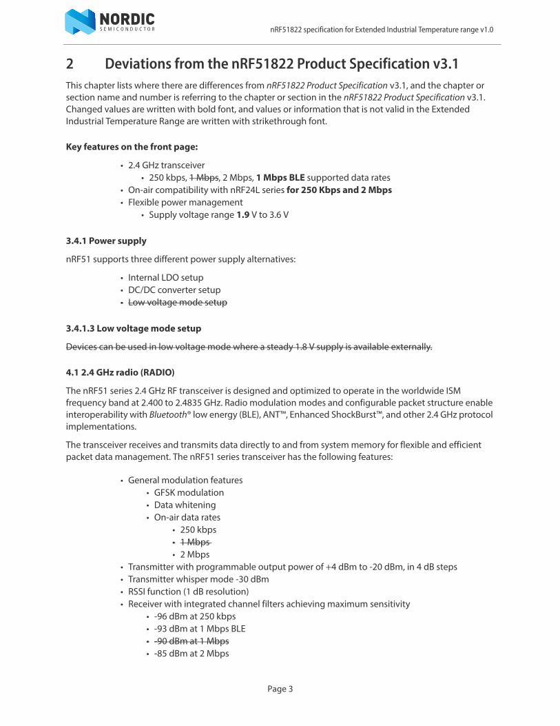
2 Deviations from the nRF51822 Product Specification v3.1This chapter lists where there are differences from nRF51822 Product Specification v3.1, and the chapter or section name and number is referring to the chapter or section in the nRF51822 Product Specification v3.1. Changed values are written with bold font, and values or information that is not valid in the Extended Industrial Temperature Range are written with strikethrough font.
Key features on the front page:
• 2.4 GHz transceiver• 250 kbps, 1 Mbps, 2 Mbps, 1 Mbps BLE supported data rates
• On-air compatibility with nRF24L series for 250 Kbps and 2 Mbps• Flexible power management
• Supply voltage range 1.9 V to 3.6 V
3.4.1 Power supply
nRF51 supports three different power supply alternatives:
• Internal LDO setup• DC/DC converter setup• Low voltage mode setup
3.4.1.3 Low voltage mode setup
Devices can be used in low voltage mode where a steady 1.8 V supply is available externally.
4.1 2.4 GHz radio (RADIO)
The nRF51 series 2.4 GHz RF transceiver is designed and optimized to operate in the worldwide ISM frequency band at 2.400 to 2.4835 GHz. Radio modulation modes and configurable packet structure enable interoperability with Bluetooth® low energy (BLE), ANT™, Enhanced ShockBurst™, and other 2.4 GHz protocol implementations.
The transceiver receives and transmits data directly to and from system memory for flexible and efficient packet data management. The nRF51 series transceiver has the following features:
• General modulation features• GFSK modulation• Data whitening• On-air data rates
• 250 kbps • 1 Mbps • 2 Mbps
• Transmitter with programmable output power of +4 dBm to -20 dBm, in 4 dB steps• Transmitter whisper mode -30 dBm• RSSI function (1 dB resolution) • Receiver with integrated channel filters achieving maximum sensitivity
• -96 dBm at 250 kbps• -93 dBm at 1 Mbps BLE• -90 dBm at 1 Mbps• -85 dBm at 2 Mbps
Page 4
nRF51822 specification for Extended Industrial Temperature range v1.0
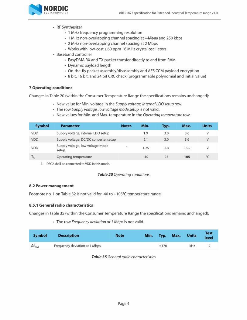
• RF Synthesizer • 1 MHz frequency programming resolution• 1 MHz non-overlapping channel spacing at 1 Mbps and 250 kbps• 2 MHz non-overlapping channel spacing at 2 Mbps• Works with low-cost ± 60 ppm 16 MHz crystal oscillators
• Baseband controller• EasyDMA RX and TX packet transfer directly to and from RAM• Dynamic payload length• On-the-fly packet assembly/disassembly and AES CCM payload encryption• 8 bit, 16 bit, and 24 bit CRC check (programmable polynomial and initial value)
7 Operating conditions
Changes in Table 20 (within the Consumer Temperature Range the specifications remains unchanged):
• New value for Min. voltage in the Supply voltage, internal LDO setup row.• The row Supply voltage, low voltage mode setup is not valid.• New values for Min. and Max. temperature in the Operating temperature row.
Table 20 Operating conditions
8.2 Power management
Footnote no. 1 on Table 32 is not valid for -40 to +105°C temperature range.
8.5.1 General radio characteristics
Changes in Table 35 (within the Consumer Temperature Range the specifications remains unchanged):
• The row Frequency deviation at 1 Mbps is not valid.
Table 35 General radio characteristics
Symbol Parameter Notes Min. Typ. Max. Units
VDD Supply voltage, internal LDO setup 1.9 3.0 3.6 V
VDD Supply voltage, DC/DC converter setup 2.1 3.0 3.6 V
VDDSupply voltage, low voltage mode setup
1
1. DEC2 shall be connected to VDD in this mode.
1.75 1.8 1.95 V
TA Operating temperature -40 25 105 °C
Symbol Description Note Min. Typ. Max. Units Testlevel
Δf1M Frequency deviation at 1 Mbps. ±170 kHz 2
Page 5
nRF51822 specification for Extended Industrial Temperature range v1.0
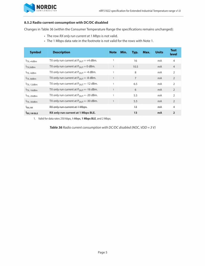
8.5.2 Radio current consumption with DC/DC disabled
Changes in Table 36 (within the Consumer Temperature Range the specifications remains unchanged):
• The row RX only run current at 1 Mbps is not valid.• The 1 Mbps data rate in the footnote is not valid for the rows with Note 1.
Table 36 Radio current consumption with DC/DC disabled (NOC, VDD = 3 V)
Symbol Description Note Min. Typ. Max. Units Testlevel
ITX,+4dBm TX only run current at POUT = +4 dBm. 1
1. Valid for data rates 250 kbps, 1 Mbps, 1 Mbps BLE, and 2 Mbps.
16 mA 4
ITX,0dBm TX only run current at POUT = 0 dBm. 1 10.5 mA 4
ITX,-4dBm TX only run current at POUT = -4 dBm. 1 8 mA 2
ITX,-8dBm TX only run current at POUT = -8 dBm. 1 7 mA 2
ITX,-12dBm TX only run current at POUT = -12 dBm. 1 6.5 mA 2
ITX,-16dBm TX only run current at POUT = -16 dBm. 1 6 mA 2
ITX,-20dBm TX only run current at POUT = -20 dBm. 1 5.5 mA 2
ITX,-30dBm TX only run current at POUT = -30 dBm. 1 5.5 mA 2
IRX,1M RX only run current at 1 Mbps. 13 mA 4
IRX,1M BLE RX only run current at 1 Mbps BLE. 13 mA 2
Page 6
nRF51822 specification for Extended Industrial Temperature range v1.0
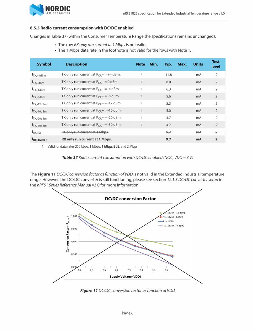
8.5.3 Radio current consumption with DC/DC enabled
Changes in Table 37 (within the Consumer Temperature Range the specifications remains unchanged):
• The row RX only run current at 1 Mbps is not valid.• The 1 Mbps data rate in the footnote is not valid for the rows with Note 1.
Table 37 Radio current consumption with DC/DC enabled (NOC, VDD = 3 V)
The Figure 11 DC/DC conversion factor as function of VDD is not valid in the Extended Industrial temperature range. However, the DC/DC converter is still functioning, please see section 12.1.3 DC/DC converter setup in the nRF51 Series Reference Manual v3.0 for more information.
Figure 11 DC/DC conversion factor as function of VDD
Symbol Description Note Min. Typ. Max. Units Testlevel
ITX,+4dBm TX only run current at POUT = +4 dBm. 1
1. Valid for data rates 250 kbps, 1 Mbps, 1 Mbps BLE, and 2 Mbps.
11.8 mA 2
ITX,0dBm TX only run current at POUT = 0 dBm. 1 8.0 mA 2
ITX,-4dBm TX only run current at POUT = -4 dBm. 1 6.3 mA 2
ITX,-8dBm TX only run current at POUT = -8 dBm. 1 5.6 mA 2
ITX,-12dBm TX only run current at POUT = -12 dBm. 1 5.3 mA 2
ITX,-16dBm TX only run current at POUT = -16 dBm. 1 5.0 mA 2
ITX,-20dBm TX only run current at POUT = -20 dBm. 1 4.7 mA 2
ITX,-30dBm TX only run current at POUT = -30 dBm. 1 4.7 mA 2
IRX,1M RX only run current at 1 Mbps. 9.7 mA 2
IRX,1M BLE RX only run current at 1 Mbps. 9.7 mA 2
0,600
0,700
0,800
0,900
1,000
1,100
2,1 2,3 2,5 2,7 2,9 3,1 3,3 3,5
Tx - 1 Mbit (-12 dBm)
Tx - 1 Mbit (0 dBm)
Rx - 1Mbit
Tx - 1 Mbit (+4 dBm)
DC/DC conversion Factor
Supply Voltage (VDD)
Conv
ersi
on F
acto
r (F D
CDC)
Page 7
nRF51822 specification for Extended Industrial Temperature range v1.0
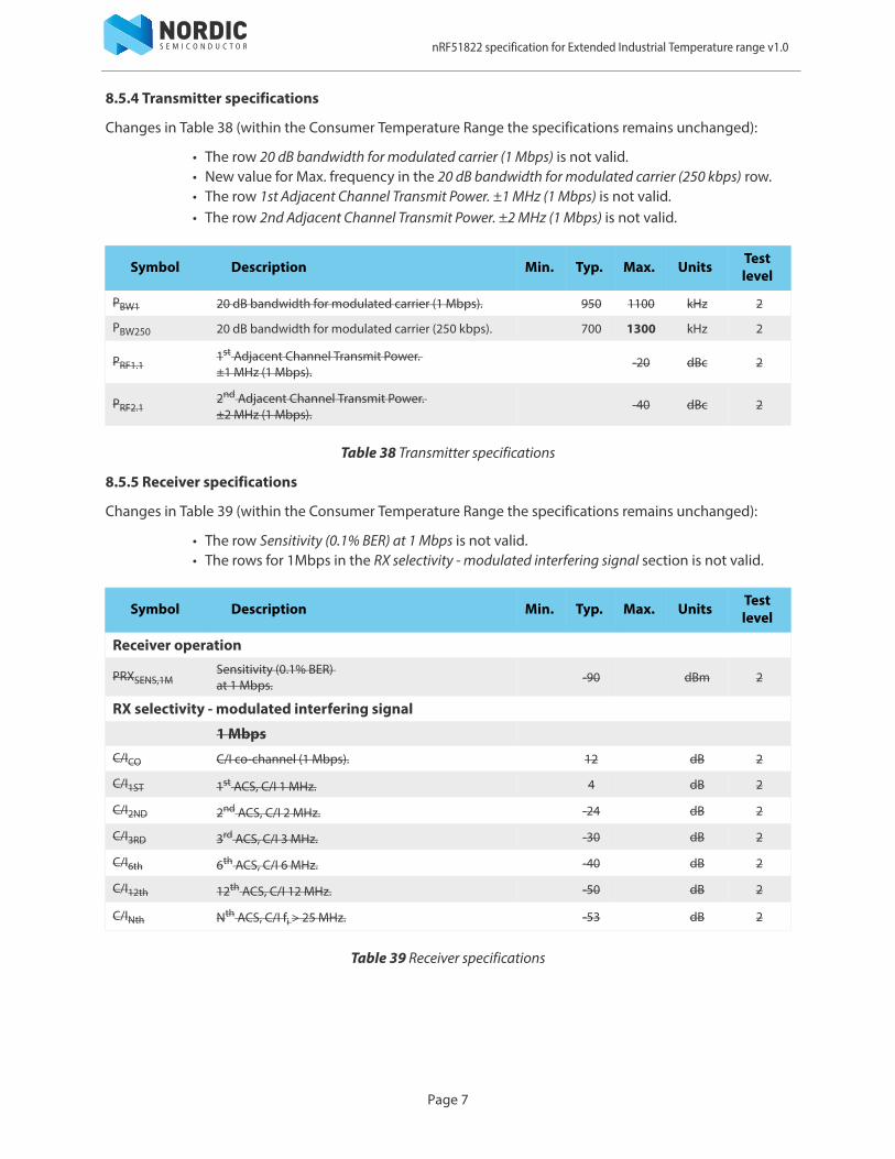
8.5.4 Transmitter specifications
Changes in Table 38 (within the Consumer Temperature Range the specifications remains unchanged):
• The row 20 dB bandwidth for modulated carrier (1 Mbps) is not valid.• New value for Max. frequency in the 20 dB bandwidth for modulated carrier (250 kbps) row.• The row 1st Adjacent Channel Transmit Power. ±1 MHz (1 Mbps) is not valid.• The row 2nd Adjacent Channel Transmit Power. ±2 MHz (1 Mbps) is not valid.
Table 38 Transmitter specifications
8.5.5 Receiver specifications
Changes in Table 39 (within the Consumer Temperature Range the specifications remains unchanged):
• The row Sensitivity (0.1% BER) at 1 Mbps is not valid.• The rows for 1Mbps in the RX selectivity - modulated interfering signal section is not valid.
Table 39 Receiver specifications
Symbol Description Min. Typ. Max. Units Testlevel
PBW1 20 dB bandwidth for modulated carrier (1 Mbps). 950 1100 kHz 2
PBW250 20 dB bandwidth for modulated carrier (250 kbps). 700 1300 kHz 2
PRF1.11st Adjacent Channel Transmit Power. ±1 MHz (1 Mbps).
-20 dBc 2
PRF2.12nd Adjacent Channel Transmit Power. ±2 MHz (1 Mbps).
-40 dBc 2
Symbol Description Min. Typ. Max. Units Testlevel
Receiver operation
PRXSENS,1MSensitivity (0.1% BER) at 1 Mbps.
-90 dBm 2
RX selectivity - modulated interfering signal
1 MbpsC/ICO C/I co-channel (1 Mbps). 12 dB 2
C/I1ST 1st ACS, C/I 1 MHz. 4 dB 2
C/I2ND 2nd ACS, C/I 2 MHz. -24 dB 2
C/I3RD 3rd ACS, C/I 3 MHz. -30 dB 2
C/I6th 6th ACS, C/I 6 MHz. -40 dB 2
C/I12th 12th ACS, C/I 12 MHz. -50 dB 2
C/INth Nth ACS, C/I fi > 25 MHz. -53 dB 2
Page 8
nRF51822 specification for Extended Industrial Temperature range v1.0
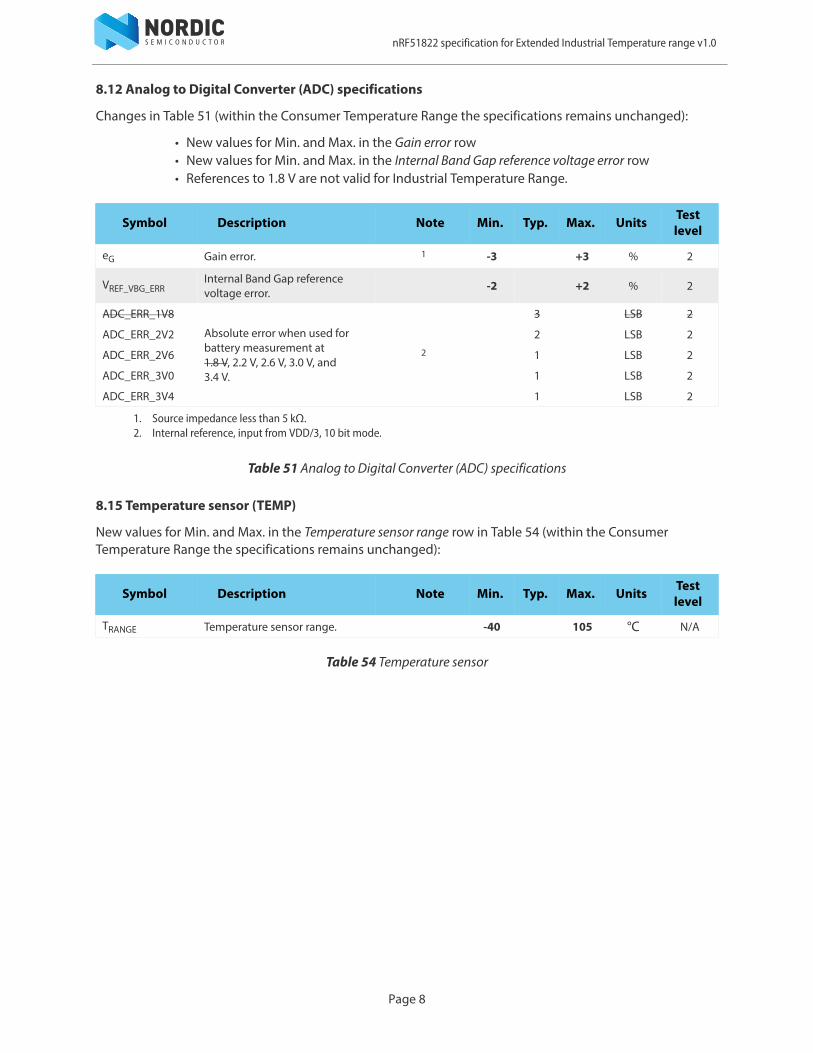
8.12 Analog to Digital Converter (ADC) specifications
Changes in Table 51 (within the Consumer Temperature Range the specifications remains unchanged):
• New values for Min. and Max. in the Gain error row• New values for Min. and Max. in the Internal Band Gap reference voltage error row• References to 1.8 V are not valid for Industrial Temperature Range.
Table 51 Analog to Digital Converter (ADC) specifications
8.15 Temperature sensor (TEMP)
New values for Min. and Max. in the Temperature sensor range row in Table 54 (within the Consumer Temperature Range the specifications remains unchanged):
Table 54 Temperature sensor
Symbol Description Note Min. Typ. Max. Units Testlevel
eG Gain error. 1
1. Source impedance less than 5 kΩ.
-3 +3 % 2
VREF_VBG_ERRInternal Band Gap referencevoltage error.
-2 +2 % 2
ADC_ERR_1V8
Absolute error when used for battery measurement at 1.8 V, 2.2 V, 2.6 V, 3.0 V, and 3.4 V.
2
2. Internal reference, input from VDD/3, 10 bit mode.
3 LSB 2
ADC_ERR_2V2 2 LSB 2
ADC_ERR_2V6 1 LSB 2
ADC_ERR_3V0 1 LSB 2
ADC_ERR_3V4 1 LSB 2
Symbol Description Note Min. Typ. Max. Units Testlevel
TRANGE Temperature sensor range. -40 105 °C N/A
Page 9
nRF51822 specification for Extended Industrial Temperature range v1.0
11.5.2 QFAA QFN48 schematic with low voltage mode setup
Not valid for -40 to +105°C temperature range.
11.8.2 CEAA WLCSP schematic with low voltage mode setup
Not valid for -40 to +105°C temperature range.
Page 10
nRF51822 specification for Extended Industrial Temperature range v1.0
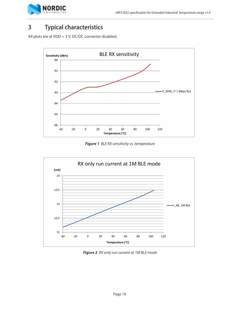
3 Typical characteristicsAll plots are at VDD = 3 V, DC/DC converter disabled.
Figure 1 BLE RX sensitivity vs. temperature
Figure 2 RX only run current at 1M BLE mode
‐96
‐95
‐94
‐93
‐92
‐91
‐90
‐40 ‐20 0 20 40 60 80 100 120
Sensitivity [dBm]
Temperature [°C]
BLE RX sensitivity
P_SENS_IT 1 Mbps BLE
12
12,5
13
13,5
14
‐40 ‐20 0 20 40 60 80 100 120
[mA]
Temperature [°C]
RX only run current at 1M BLE mode
I_RX, 1M BLE

Page 11
nRF51822 specification for Extended Industrial Temperature range v1.0
Figure 3 POUT in 0 dBm mode.
Figure 4 TX only run current at POUT = 0 dBm.
‐3
‐2
‐1
0
1
2
3
‐40 ‐20 0 20 40 60 80 100 120
[dBm]
Temperature [°C]
POUT in 0 dBm mode
POUT in 0dBm mode
10,2
10,3
10,4
10,5
10,6
10,7
10,8
10,9
11
11,1
11,2
11,3
‐40 ‐20 0 20 40 60 80 100 120
[mA]
Temperature [°C]
TX only run current at POUT = 0 dBm
I_TX,0dBm

Page 12
nRF51822 specification for Extended Industrial Temperature range v1.0
Liability disclaimerNordic Semiconductor ASA reserves the right to make changes without further notice to the product to improve reliability, function or design. Nordic Semiconductor ASA does not assume any liability arising out of the application or use of any product or circuits described herein.
Life support applicationsNordic Semiconductor’s products are not designed for use in life support appliances, devices, or systems where malfunction of these products can reasonably be expected to result in personal injury. Nordic Semiconductor ASA customers using or selling these products for use in such applications do so at their own risk and agree to fully indemnify Nordic Semiconductor ASA for any damages resulting from such improper use or sale.
Contact detailsFor your nearest distributor, please visit www.nordicsemi.com.Information regarding product updates, downloads, and technical support can be accessed through your My Page account on our home page.
RoHS and REACH statementNordic Semiconductor's products meet the requirements of Directive 2002/95/EC of the European Parliament and of the Council on the Restriction of Hazardous Substances (RoHS) and the requirements of the REACH regulation (EC 1907/2006) on Registration, Evaluation, Authorization and Restriction of Chemicals. The SVHC (Substances of Very High Concern) candidate list is continually being updated. Complete hazardous substance reports, material composition reports and latest version of Nordic's REACH statement can be found on our website www.nordicsemi.com.
Main office:
Phone: +47 72 89 89 00Fax: +47 72 89 89 89
Otto Nielsens veg 127052 TrondheimNorway
Mailing address: Nordic SemiconductorP.O. Box 23367004 TrondheimNorway

Page 13
nRF51822 specification for Extended Industrial Temperature range v1.0
Revision History
Date Version Description
June 2015 1.0 First release.