ntag 203 datasheet
DESCRIPTION
NTAG 203 datasheetTRANSCRIPT
1. General description
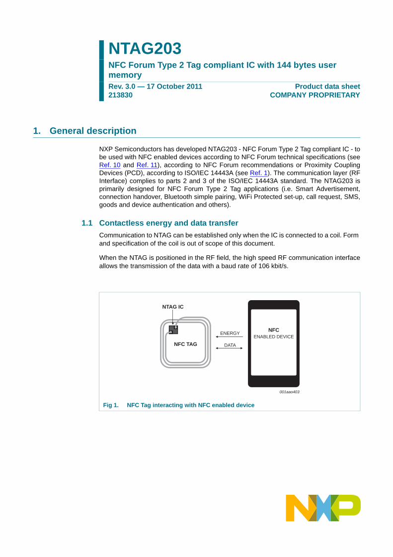
NXP Semiconductors has developed NTAG203 - NFC Forum Type 2 Tag compliant IC - tobe used with NFC enabled devices according to NFC Forum technical specifications (seeRef. 10 and Ref. 11), according to NFC Forum recommendations or Proximity CouplingDevices (PCD), according to ISO/IEC 14443A (see Ref. 1). The communication layer (RFInterface) complies to parts 2 and 3 of the ISO/IEC 14443A standard. The NTAG203 isprimarily designed for NFC Forum Type 2 Tag applications (i.e. Smart Advertisement,connection handover, Bluetooth simple pairing, WiFi Protected set-up, call request, SMS,goods and device authentication and others).
1.1 Contactless energy and data transfer
Communication to NTAG can be established only when the IC is connected to a coil. Form and specification of the coil is out of scope of this document.
When the NTAG is positioned in the RF field, the high speed RF communication interfaceallows the transmission of the data with a baud rate of 106 kbit/s.
NTAG203NFC Forum Type 2 Tag compliant IC with 144 bytes user memoryRev. 3.0 — 17 October 2011213830
Product data sheetCOMPANY PROPRIETARY
Fig 1. NFC Tag interacting with NFC enabled device
001aao403
ENERGY
DATA
NFCENABLED DEVICE
NFC TAG
NTAG IC
NXP Semiconductors NTAG203NFC Forum Type 2 Tag compliant IC with 144 bytes user memory
1.2 Naming conventions
2. Features and benefits
2.1 RF Interface (ISO/IEC 14443A)
Contactless transmission of data and supply energy (no battery needed)
Operating distance: up to 100 mm (depending on field strength and antenna geometry)
Operating frequency: 13.56 MHz
Fast data transfer: 106 kbit/s
High data integrity: 16-bit CRC, parity, bit coding, bit counting
True anticollision
7 byte serial number (cascade level 2 according to ISO/IEC 14443-3)
2.2 EEPROM
168 bytes of total memory, divided in 42 pages (4 bytes each)
144 bytes of user r/w memory area, divided in 36 pages (4 bytes each)
Field programmable read-only locking function per page for first 64 bytes
Field programmable read-only locking function per block
32-bit user definable One-Time Programmable (OTP) area
16-bit counter
Data retention of 5 years
Write endurance 10000 cycles
2.3 NFC Forum Tag 2 Type compliance
NTAG203 IC provides full compliance to the NFC Forum Tag 2 Type technicalspecification (see Ref. 10) and enables NDEF data structure configurations (see Ref. 11).
2.4 Security
Anti-cloning support by unique 7-byte serial number for each device
32-bit user programmable OTP area
Field programmable read-only locking function per page for first 512 bits
Read-only locking per block for rest of memory
Table 1. Short naming convention (for easier product identification)
Family name Description
NTAG NXP NFC Tag product family name
2 Platform indicator
0 Generation number (starting from 0)
3 Code number for memory size (0 : < 64 bytes, 1 : 64-96 bytes; 2 : 96-128 bytes; 3 : 128-256 bytes)
F Delivery option: if stated, it is a HWSON8 package with Field Detection pin
NTAG203 All information provided in this document is subject to legal disclaimers. © NXP B.V. 2011. All rights reserved.
Product data sheetCOMPANY PROPRIETARY
Rev. 3.0 — 17 October 2011213830 2 of 30

NXP Semiconductors NTAG203NFC Forum Type 2 Tag compliant IC with 144 bytes user memory
2.5 Cascaded UID
The anticollision function is based on an IC individual serial number called UniqueIDentifier. The UID of the NTAG203 is 7 bytes long and supports cascade level 2according to ISO/IEC 14443-3.
2.6 Anticollision
An intelligent anticollision function according to ISO/IEC 14443 allows to operate morethan one card in the field simultaneously. The anticollision algorithm selects each cardindividually and ensures that the execution of a transaction with a selected card isperformed correctly without data corruption resulting from other cards in the field.
3. Ordering information
4. Block diagram
5. Pinning information
5.1 Pin description
This section is not applicable for this device.
Table 2. Ordering information
Type number Package
Name Description Version
MF0ICU1701NDUD wafer 8 inch wafer (sawn, laser diced; 120 m thickness, on film frame carrier; electronic fail die marking according to SECSII format)
-
Fig 2. Block diagram
001aal339
antenna RF INTERFACE
DIGITAL CONTROL UNIT
EEPROMANTICOLLISION
COMMANDINTERPRETER
EEPROMINTERFACE
NTAG203 All information provided in this document is subject to legal disclaimers. © NXP B.V. 2011. All rights reserved.
Product data sheetCOMPANY PROPRIETARY
Rev. 3.0 — 17 October 2011213830 3 of 30

NXP Semiconductors NTAG203NFC Forum Type 2 Tag compliant IC with 144 bytes user memory
6. Wafer layout
(1) Y-Scribeline width: 15 m
(2) X-Scribeline width: 15 m
(3) Chip step, x-length: 688 m
(4) Chip step, y-length: 688 m
(5) LA bump edge to chip edge, y-length: 14.9 m
(6) LA bump edge to chip edge, x-length: 15 m
(7) LB bump edge to chip edge, y-length: 21.296 m
(8) LB bump edge to chip edge, x-length: 15 m
Remark: Lower left corner of metal sealring (X, Y) = 0,0
Remark: The scribeline width is not constant for laser diced wafers.
Fig 3. Chip orientation and bond pad locations
Table 3. Bonding pad assignments to smart card contactless module
Contactless interface module NTAG203
Antenna contacts Symbol Description
LA LA Antenna coil connection LA
LB LB Antenna coil connection LB
001aaj821
TEST
Y
X
VSSTEST LB
LA
(2)
(3)
(4)
(1)
(5)
(7)
(8)
(6)
PAD(center)
X[μm]
Y[μm]
VSS, TEST DISCONNECTED
LA 45.5 628
LB 628 51.1
NTAG203 All information provided in this document is subject to legal disclaimers. © NXP B.V. 2011. All rights reserved.
Product data sheetCOMPANY PROPRIETARY
Rev. 3.0 — 17 October 2011213830 4 of 30

NXP Semiconductors NTAG203NFC Forum Type 2 Tag compliant IC with 144 bytes user memory
7. Mechanical specification
Remark: Substrate is connected to VSS.
Table 4. Wafer specifications
Wafer
diameter 8” wafer, 200 mm unsawn
min: 200 mm
typ: 206 mm
max: 210 mm
thickness 120 m 15 m
flatness not applicable
Potential Good Dies per Wafer (PGDW) 61942
Sawing method laser dicing
Wafer backside
material Si
treatment ground and stress relieve
roughness Ra max 0.2 m
Rt max 2 m
Chip dimensions
chip size 0.673 mm 0.673 mm
scribe lines x-line:15 m 5 m
y-line:15 m 5 m
Passivation
type sandwich structure
material Nitride
thickness 1.75 m
Au bump
material > 99.9 % pure Au
hardness 35 – 80 HV 0.005
shear strength > 70 MPa
height 18 m
height uniformity
within a die 2 m
within a wafer 3 m
wafer to wafer 4 m
flatness 1.5 m
size
LA, LB 60 m 60 m
TP1, TP2, VSS 60 m 60 m
size variation 5 m
under bump metallization sputtered TiW
NTAG203 All information provided in this document is subject to legal disclaimers. © NXP B.V. 2011. All rights reserved.
Product data sheetCOMPANY PROPRIETARY
Rev. 3.0 — 17 October 2011213830 5 of 30

NXP Semiconductors NTAG203NFC Forum Type 2 Tag compliant IC with 144 bytes user memory
7.1 Fail die identification
Electronic wafer mapping covers the electrical test results and additionally the results of mechanical/ visual inspection.
No inkdots are applied.
8. Functional description
8.1 Block description
The NTAG203 chip consists of the 168 bytes of the total memory organized in 42 usermemory EEPROM. From that amount, 144 bytes (36 pages) are available for the userdefined data.
Along with the memory, NTAG203 contains the RF-Interface and the Digital Control Unit.Energy and data are transferred via an antenna, which consists of a coil with a few turnsdirectly connected to the LA and LB of the NTAG203 (see Section 5 for details). No furtherexternal components are necessary. (For details on antenna design please refer to thedocument Ref. 6 “(Card) Coil Design Guide”.)
NTAG203 All information provided in this document is subject to legal disclaimers. © NXP B.V. 2011. All rights reserved.
Product data sheetCOMPANY PROPRIETARY
Rev. 3.0 — 17 October 2011213830 6 of 30
NXP Semiconductors NTAG203NFC Forum Type 2 Tag compliant IC with 144 bytes user memory
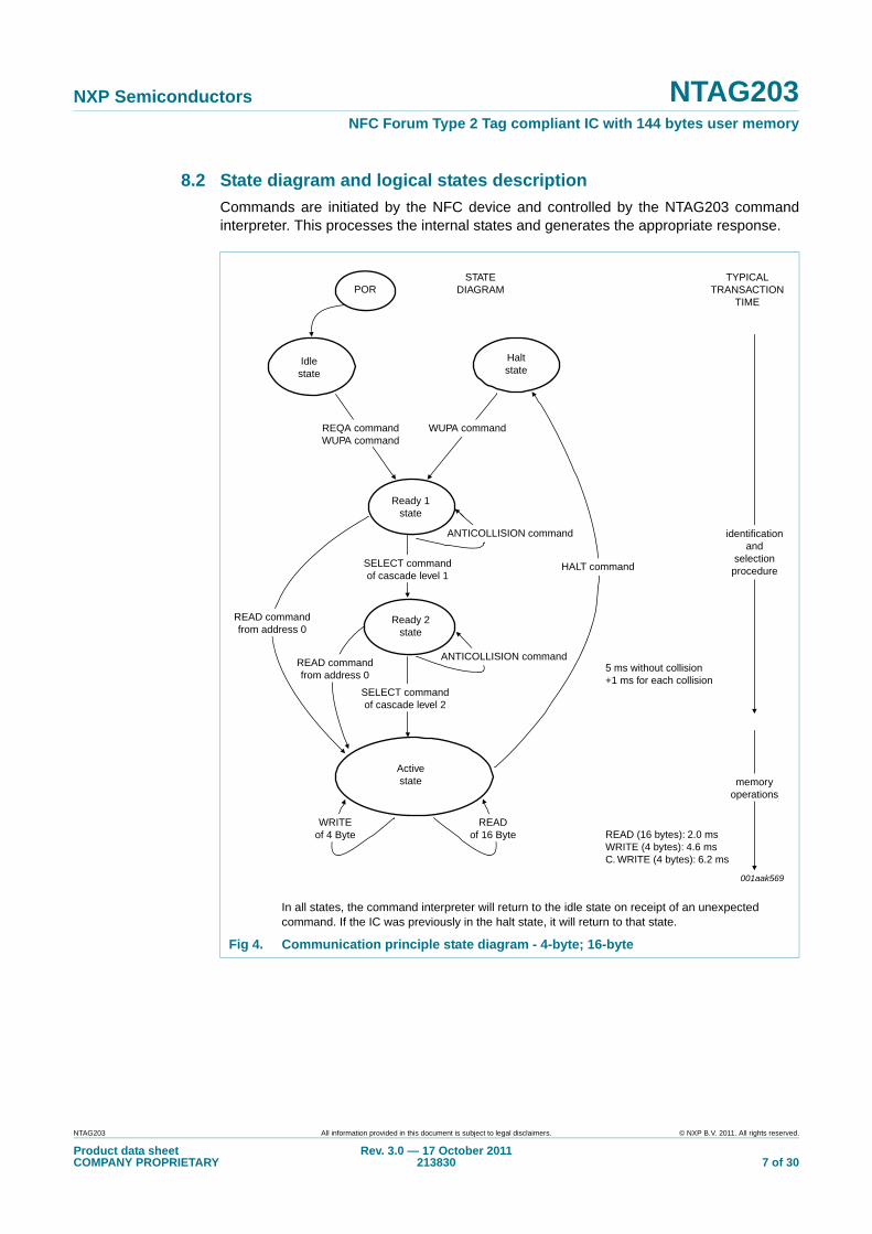
8.2 State diagram and logical states description
Commands are initiated by the NFC device and controlled by the NTAG203 commandinterpreter. This processes the internal states and generates the appropriate response.
In all states, the command interpreter will return to the idle state on receipt of an unexpected command. If the IC was previously in the halt state, it will return to that state.
Fig 4. Communication principle state diagram - 4-byte; 16-byte
001aak569
POR
Idlestate
Haltstate
STATEDIAGRAM
TYPICALTRANSACTION
TIME
5 ms without collision+1 ms for each collision
READ (16 bytes): 2.0 msWRITE (4 bytes): 4.6 msC. WRITE (4 bytes): 6.2 ms
Ready 1state
Ready 2state
Activestate
ANTICOLLISION command
ANTICOLLISION command
READof 16 Byte
WRITEof 4 Byte
READ commandfrom address 0
READ commandfrom address 0
SELECT commandof cascade level 1
SELECT commandof cascade level 2
WUPA command
HALT command
REQA commandWUPA command
memoryoperations
identificationand
selectionprocedure
NTAG203 All information provided in this document is subject to legal disclaimers. © NXP B.V. 2011. All rights reserved.
Product data sheetCOMPANY PROPRIETARY
Rev. 3.0 — 17 October 2011213830 7 of 30
NXP Semiconductors NTAG203NFC Forum Type 2 Tag compliant IC with 144 bytes user memory
8.2.1 Idle state
After a Power-On Reset (POR), the NTAG203 switches directly to the idle state. It onlyexits this state when a REQA or a WUPA command is received from the NFC device. Anyother data received while in the idle state is interpreted as an error and the NTAG203remains Idle.
After a correctly executed HALT command, the halt state changes to the wait state whichcan be exited with a WUPA command.
8.2.2 Ready1 state
In this state, the NTAG203 supports the NFC device when resolving the first part of its UID(3 bytes) with the ANTICOLLISION or SELECT command from cascade level 1. This stateis exited correctly after execution of either of the following commands:
• SELECT command from cascade level 1: the NFC device switches NTAG203 into Ready2 state where the second part of the UID is resolved.
• READ command (from address 0): all anticollision mechanisms are bypassed and NTAG203 switches directly to the active state.
Remark: If more than one NTAG203 is in the NFC device field, a READ command fromaddress 0 causes a collision due to the different serial numbers and all NTAG203 devicesare selected. Any other data received in the Ready1 state is interpreted as an error anddepending on its previous state the NTAG203 returns to the wait, idle or halt state.
8.2.3 Ready2 state
In this state, the NTAG203 supports the NFC device when resolving the second part of itsUID (4 bytes) with the cascade level 2 ANTICOLLISION command. This state is usuallyexited using the cascade level 2 SELECT command.
Alternatively, state Ready2 may be skipped using a READ command (from address 0) asdescribed in state Ready1.
Remark: If more than one NTAG203 is in the NFC device field, a READ command fromaddress 0 causes a collision due to the different serial numbers and all NTAG203 devicesare selected. The response of the NTAG203 to the cascade level 2 SELECT command isthe Select Acknowledge (SAK) byte. In accordance with ISO/IEC 14443 this byteindicates if the anticollision cascade procedure has finished. It also defines the type ofdevice selected for the MIFARE architecture platform. The NTAG203 is now uniquelyselected and only this device will communicate with the NFC device even when othercontactless devices are present in the NFC device field. Any other data received when thedevice is in this state is interpreted as an error and depending on its previous state theNTAG203 returns to the wait, idle or halt state.
8.2.4 Active state
In the active state either a 16-byte READ or 4-byte WRITE command can be performed.The HALT command exits either the READ or WRITE commands in their active state. Anyother data received when the device is in this state is interpreted as an error anddepending on its previous state the NTAG203 returns to the wait, idle or halt state.
NTAG203 All information provided in this document is subject to legal disclaimers. © NXP B.V. 2011. All rights reserved.
Product data sheetCOMPANY PROPRIETARY
Rev. 3.0 — 17 October 2011213830 8 of 30
NXP Semiconductors NTAG203NFC Forum Type 2 Tag compliant IC with 144 bytes user memory
8.2.5 Halt state
The halt and idle states constitute the second wait state implemented in the NTAG203. Analready processed NTAG203 can be set into the halt state using the HALT command. Inthe anticollision phase, this state helps the NFC device to distinguish between processedcards and cards yet to be selected. The NTAG203 can only exit this state on execution ofthe WUPA command. Any other data received when the device is in this state isinterpreted as an error and the NTAG203 state is unchanged. Refer to the documentMIFARE collection of currently available application notes for correct implementation of ananticollision procedure based on the idle and halt states and the REQA and WUPAcommands.
8.3 Data integrity
The following mechanisms are implemented in the contactless communication linkbetween NFC device and NTAG203 to ensure a reliable data transmission:
• 16 bits CRC per block
• Parity bit for each byte
• Bit count checking
• Bit coding to distinguish between "1", "0", and no information
• Channel monitoring (protocol sequence and bit stream analysis)
8.4 RF interface
The RF-interface is according to the standard for contactless smart cardsISO/IEC 14443A (see Ref. 1 “ISO/IEC”).
The RF-field from the NFC device is always present (with short modulation pulses whentransmitting), because it is used for the power supply of the card.
For both directions of data communication there is one start bit at the beginning of eachframe. Each byte is transmitted with a parity bit (odd parity) at the end. The LSBit of thebyte with the lowest address of the selected block is transmitted first. The maximum framelength is 164 bits (16 data bytes + 2 CRC bytes = 16 * 9 + 2 * 9 + 1 start bit + 1 end bit).
NTAG203 All information provided in this document is subject to legal disclaimers. © NXP B.V. 2011. All rights reserved.
Product data sheetCOMPANY PROPRIETARY
Rev. 3.0 — 17 October 2011213830 9 of 30
NXP Semiconductors NTAG203NFC Forum Type 2 Tag compliant IC with 144 bytes user memory
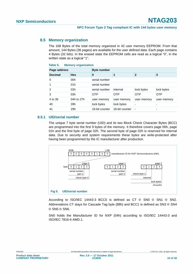
8.5 Memory organization
The 168 Bytes of the total memory organized in 42 user memory EEPROM. From thatamount, 144 Bytes (36 pages) are available for the user defined data. Each page contains4 Bytes (32 bits). In the erased state the EEPROM cells are read as a logical “0”, in thewritten state as a logical “1”.
8.5.1 UID/serial number
The unique 7 byte serial number (UID) and its two Block Check Character Bytes (BCC)are programmed into the first 9 bytes of the memory. It therefore covers page 00h, page01h and the first byte of page 02h. The second byte of page 02h is reserved for internaldata. Due to security and system requirements these bytes are write-protected afterhaving been programmed by the IC manufacturer after production.
According to ISO/IEC 14443-3 BCC0 is defined as CT SN0 SN1 SN2.
Abbreviations CT stays for Cascade Tag byte (88h) and BCC1 is defined as SN3 SN4
SN5 SN6.
SN0 holds the Manufacturer ID for NXP (04h) according to ISO/IEC 14443-3 andISO/IEC 7816-6 AMD.1.
Table 5. Memory organization
Page address Byte number
Decimal Hex 0 1 2 3
0 00h serial number
1 01h serial number
2 02h serial number internal lock bytes lock bytes
3 03h OTP OTP OTP OTP
4 to 39 04h to 27h user memory user memory user memory user memory
40 28h lock bytes lock bytes - -
41 29h 16-bit counter 16-bit counter - -
Fig 5. UID/serial number
001aai001
MSB LSB
page 0
byte
check byte 0
serial numberpart 1
serial numberpart 2
manufacturer ID for NXP Semiconductors (04h)0 0 0 0 0 1 0 0
0 1 2 3
page 1
0 1 2 3
page 2
0 1 2 3
internal
check byte 1
lock bytes
NTAG203 All information provided in this document is subject to legal disclaimers. © NXP B.V. 2011. All rights reserved.
Product data sheetCOMPANY PROPRIETARY
Rev. 3.0 — 17 October 2011213830 10 of 30

NXP Semiconductors NTAG203NFC Forum Type 2 Tag compliant IC with 144 bytes user memory
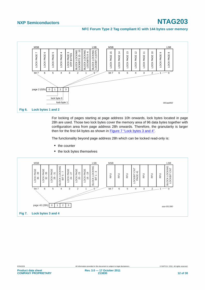
8.5.2 Lock bytes
Lock bytes enable the user to lock parts of the complete memory area for writing. A Readfrom user memory area cannot be restricted via lock bytes functionality.
The lock bytes functionality is enabled with a WRITE command (see Section 8.8.7“WRITE”) or COMPATIBILITY WRITE command (see Section 8.8.8 “COMPATIBILITYWRITE”), where 2 out of 4 bytes transmitted are used for setting the lock bytes. Twocorresponding bytes - either bytes 2 and 3 for page 02h or bytes 0 and 1 for page 28h -and the actual content of the lock bytes are bit-wise “OR-ed”. The result of OR operationbecomes the new content of the lock bytes. Two unused bytes do not have to beconsidered. Although included in the COMPATIBILITY WRITE or WRITE command, theyare ignored when programming the memory.
Due to the built-in bitwise OR operation, this process is irreversible. If a bit is set to “1”, itcannot be changed back to “0” again. Therefore, before locking the lock bytes, the usermust ensure that the corresponding user memory area and/or configuration bytes arecorrectly written.
The configuration written in the lock bytes is active upon the next REQA or WUPAcommand.
The single bits of the 4 bytes available for locking incorporate 3 different functions:
• the read-only locking of the single pages or blocks of the user memory area
• the read-only locking of the single bytes of the configuration memory area
• the locking of the lock bits themselves
For the compatibility reasons, the first 64 bytes (512 bits) of the memory area have thesame functionality as MIFARE Ultralight (MF0ICU1, see also Ref. 7), meaning that the twolock bytes used for the configuration of this memory area are identically configured. Themapping of single bits to memory area for the first 64 bytes (512 bits) is shown in Figure 6.
The bits of byte 2 and 3 of page 02h represent the field-programmable read-only lockingmechanism. Each page x from 03h (OTP bits) to 0Fh may be locked individually toprevent further write access by setting the corresponding locking bit Lx to 1. After lockingthe page is read-only memory.
The 3 least significant bits of lock byte 0 of page 2 are the block-locking bits. Bit 2 handlespages 0Fh to 0Ah, bit 1 pages 09h to 04h and bit 0 page 03h (OTP bits). Once the blocklocking bits are set, the locking configuration for the corresponding memory area is frozen.
Table 6. Lock bytes
Name Page Function
Number Address
Lock byte 0 2 02h page and block locking
Lock byte 1 2 02h page locking
Lock byte 2 40 28h page and block locking
Lock byte 3 40 28h functionality and block locking
NTAG203 All information provided in this document is subject to legal disclaimers. © NXP B.V. 2011. All rights reserved.
Product data sheetCOMPANY PROPRIETARY
Rev. 3.0 — 17 October 2011213830 11 of 30
NXP Semiconductors NTAG203NFC Forum Type 2 Tag compliant IC with 144 bytes user memory
For locking of pages starting at page address 10h onwards, lock bytes located in page28h are used. Those two lock bytes cover the memory area of 96 data bytes together withconfiguration area from page address 28h onwards. Therefore, the granularity is largerthen for the first 64 bytes as shown in Figure 7 “Lock bytes 3 and 4”.
The functionality beyond page address 28h which can be locked read-only is:
• the counter
• the lock bytes themselves
Fig 6. Lock bytes 1 and 2
001aai002
BLO
CK
LO
CK
ING
LOC
KB
ITS
15
- 10
BLO
CK
LO
CK
ING
LOC
KB
ITS
9 -
4
BLO
CK
LO
CK
ING
LOC
KB
IT 3
(O
TP
)
LOC
K P
AG
E 3
OT
P B
YT
ES
LOC
K P
AG
E 7
LOC
K P
AG
E 6
LOC
K P
AG
E 5
LOC
K P
AG
E 4
LOC
K P
AG
E 1
5
LOC
K P
AG
E 1
4
LOC
K P
AG
E 1
3
LOC
K P
AG
E 1
2
LOC
K P
AG
E 1
1
LOC
K P
AG
E 1
0
LOC
K P
AG
E 9
LOC
K P
AG
E 8
MSB
6 5 4 3 2 1 bit 7 6 5 4 3 2
LSB MSB LSB
page 2 (02h) 10 2 3
lock byte 0
lock byte 1
010bit 7
Fig 7. Lock bytes 3 and 4
aaa-001380
BLO
CK
LO
CK
ING
BIT
1 -
3
LOC
K P
AG
E36
- 39
LOC
K P
AG
E32
- 35
LOC
K P
AG
E28
- 31
BLO
CK
LO
CK
ING
BIT
5 -
7
LOC
K P
AG
E24
- 27
LOC
K P
AG
E20
- 23
LOC
K P
AG
E16
- 19
RFU
RFU
RFU
BLO
CK
LO
CK
ING
LOC
KB
IT C
NT
RFU
RFU
LOC
KB
IT C
NT
PAG
E 4
1
RFU
MSB
6 5 4 3 2 1 bit 7 6 5 4 3 2
LSB MSB LSB
page 40 (28h) 10 2 3
010bit 7
NTAG203 All information provided in this document is subject to legal disclaimers. © NXP B.V. 2011. All rights reserved.
Product data sheetCOMPANY PROPRIETARY
Rev. 3.0 — 17 October 2011213830 12 of 30
NXP Semiconductors NTAG203NFC Forum Type 2 Tag compliant IC with 144 bytes user memory
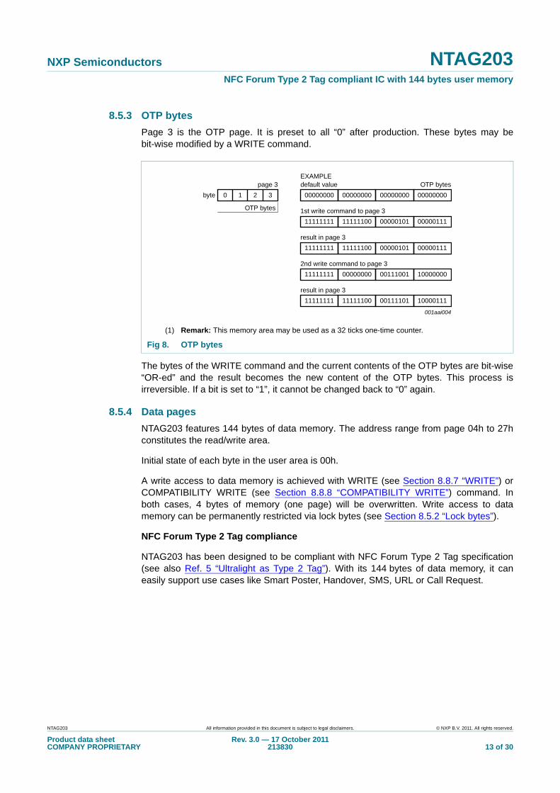
8.5.3 OTP bytes
Page 3 is the OTP page. It is preset to all “0” after production. These bytes may bebit-wise modified by a WRITE command.
The bytes of the WRITE command and the current contents of the OTP bytes are bit-wise“OR-ed” and the result becomes the new content of the OTP bytes. This process isirreversible. If a bit is set to “1”, it cannot be changed back to “0” again.
8.5.4 Data pages
NTAG203 features 144 bytes of data memory. The address range from page 04h to 27hconstitutes the read/write area.
Initial state of each byte in the user area is 00h.
A write access to data memory is achieved with WRITE (see Section 8.8.7 “WRITE”) orCOMPATIBILITY WRITE (see Section 8.8.8 “COMPATIBILITY WRITE”) command. Inboth cases, 4 bytes of memory (one page) will be overwritten. Write access to datamemory can be permanently restricted via lock bytes (see Section 8.5.2 “Lock bytes”).
NFC Forum Type 2 Tag compliance
NTAG203 has been designed to be compliant with NFC Forum Type 2 Tag specification(see also Ref. 5 “Ultralight as Type 2 Tag”). With its 144 bytes of data memory, it caneasily support use cases like Smart Poster, Handover, SMS, URL or Call Request.
(1) Remark: This memory area may be used as a 32 ticks one-time counter.
Fig 8. OTP bytes
001aai004
page 3 default valueEXAMPLE
OTP bytes
byte
OTP bytes
0 1 2 3 00000000 00000000 00000000 00000000
1st write command to page 3
11111111 11111100 00000101 00000111
result in page 3
11111111 11111100 00000101 00000111
2nd write command to page 3
11111111 00000000 00111001 10000000
result in page 3
11111111 11111100 00111101 10000111
NTAG203 All information provided in this document is subject to legal disclaimers. © NXP B.V. 2011. All rights reserved.
Product data sheetCOMPANY PROPRIETARY
Rev. 3.0 — 17 October 2011213830 13 of 30

NXP Semiconductors NTAG203NFC Forum Type 2 Tag compliant IC with 144 bytes user memory
8.5.5 Initial memory configuration
The memory configuration of NTAG203 in delivery state is shown in Table 7 “Initialmemory organization”:
The memory configuration in pages 3 to 5 ensures that NTAG203 is a NFC forum Type 2Tag in INITIALIZED state according to the NFC Forum Technical Specification, Ref. 10“Tag 2 Type Operation, Technical Specification”. It is recommended that any furthermodification of the memory pages 2 to 40 should be according to the Ref. 10 “Tag 2 TypeOperation, Technical Specification”.
All lock bytes are set to zero meaning that no page or functionality is locked. Counter is set to zero.
Table 7. Initial memory organization
Page address Byte number
dec. hex. 0 1 2 3
0 00h UID0 UID1 UID2 BCC0
1 01h UID3 UID4 UID5 UID6
2 02h BCC1 internal 00h 00h
3 03h E1h 10h 12h 00h
4 04h 01h 03h A0h 10h
5 05h 44h 03h 00h FEh
6 to 39 06h to 27h 00h 00h 00h 00h
40 28h 00h 00h rfu rfu
41 29h 00h 00h rfu rfu
NTAG203 All information provided in this document is subject to legal disclaimers. © NXP B.V. 2011. All rights reserved.
Product data sheetCOMPANY PROPRIETARY
Rev. 3.0 — 17 October 2011213830 14 of 30

NXP Semiconductors NTAG203NFC Forum Type 2 Tag compliant IC with 144 bytes user memory
8.6 Counter
NTAG203 features 16-bit one-way counter, located at first two bytes of page 29h. In itsdelivery state, counter value is set to 0000h.
The first1 valid Write or Compatibility write to the address 29h can be performed with anyvalue in the range between 0001h and FFFFh and corresponds to initial counter value.Every consequent valid WRITE command, which represents the increment, can containvalues between 0001h and 000Fh. Upon such WRITE command and following mandatoryRF reset, the value written to the address 29h is added to the counter content.
If - after initial write - a value higher then 000Fh is used as a parameter, NTAG203 willanswer with NAK. Once counter value reaches FFFFh and an increment is performed viavalid command, NTAG203 will answer with NAK. If the sum of counter value andincrement is higher than FFFFh, NTAG203 will answer with NAK and will not update thecounter.
Increment by zero (00h) is always possible, but does not have any impact to countervalue.
8.7 PICC response to a command from NFC device
NFC Tag Type 2 compliant IC uses, apart from the responses defined in the followingsections, two half-byte answers to acknowledge the command received in Active state(see Figure 4 “Communication principle state diagram - 4-byte; 16-byte”).
NFC Tag Type 2 compliant IC distinguishes between positive (ACK) and negative (NAK)acknowledge. Valid values for ACK and NAK are shown in Table 8 “ACK and NAKvalues”.
After every NAK, NTAG203 will perform an internal reset.
1. First valid write is defined as write to a counter value of zero with an argument different then zero
Table 8. ACK and NAK values
Answer value Answer explanation
Ah positive acknowledge (ACK)
1h parity or CRC error (NAK)
0h any other error (NAK)
NTAG203 All information provided in this document is subject to legal disclaimers. © NXP B.V. 2011. All rights reserved.
Product data sheetCOMPANY PROPRIETARY
Rev. 3.0 — 17 October 2011213830 15 of 30

NXP Semiconductors NTAG203NFC Forum Type 2 Tag compliant IC with 144 bytes user memory
8.8 Command set
The ATQA and SAK are identical as for MIFARE Ultralight (see Ref. 7 “MF0ICU1Functional specification MIFARE Ultralight”). For information on ISO 14443 cardactivation, see Ref. 3 “ISO/IEC 14443 PICC Selection”. Summary of data relevant fordevice identification is given in Section 8.9 “Summary of relevant data for deviceidentification”.
The NTAG203 comprises the command set as described in following chapters.
8.8.1 REQA
Description: The NTAG203 accepts the REQA command in Idle state only. The responseis the 2-byte ATQA (0044h). REQA and ATQA are implemented fully according toISO/IEC 14443-3.
8.8.2 WUPA
Description: NTAG203 accepts the WUPA command in the Idle and Halt state only. Theresponse is the 2-byte ATQA (0044h). WUPA is implemented fully according to ISO/IEC14443-3.
Table 9. REQA
Code Parameter Data Integrity mechanism Response
26h (7-bit) - - Parity 0044h
Remark: Time units are not to scale and rounded off to 10 s
Fig 9. REQA
aaa-001143
CMD (7 bit)
ATQA
80 ms
RWDcommand
timeNTAG
response
90 ms 170 ms
26
44 00
Table 10. WUPA
Code Parameter Data Integrity mechanism Response
52h (7-bit) - - Parity 0044h
Remark: Time units are not to scale and rounded off to 10 s
Fig 10. WUPA
aaa-001144
CMD (7 bit)
ATQA
70 ms
RWDcommand
timeNTAG
response
90 ms 170 ms
52
44 00
NTAG203 All information provided in this document is subject to legal disclaimers. © NXP B.V. 2011. All rights reserved.
Product data sheetCOMPANY PROPRIETARY
Rev. 3.0 — 17 October 2011213830 16 of 30

NXP Semiconductors NTAG203NFC Forum Type 2 Tag compliant IC with 144 bytes user memory
8.8.3 ANTICOLLISION and SELECT of cascade level 1
Description: The ANTICOLLISION and SELECT commands are based on the samecommand code. They differ only in the Parameter byte. This byte is per definition 70h incase of SELECT. NTAG203 accepts these commands in the Ready1 state only. Theresponse is part 1 of the UID. Even with incorrect CRC value, the SELECT command willbe fully functional.
Table 11. ANTICOLLISION and SELECT of cascade level 1
Code Parameter Data Integrity mechanism Response
Anticollision: 93h 20h - Parity, BCC -
Anticollision: 93h 21h to 67h Part of the UID Parity, BCC Parts of UID
Select: 93h 70h First 3 bytes of UID Parity, BCC, CRC SAK (‘04’)
Remark: Time units are not to scale and rounded off to 10 s
Fig 11. ANTICOLLISION of cascade level 1
aaa-001145
CMD
CT UID of cascade level 1
180 ms
RWDcommand
timeNTAG
response
90 ms 430 ms
93
ARG
20
88 SN0 SN1 SN2 BCC1
Remark: Time units are not to scale and rounded off to 10 s
Fig 12. SELECT of cascade level 1
aaa-001146
CMD
SAK CRC
780 ms
RWDcommand
timeNTAG
response
90 ms 260 ms
93
ARG CT CRCUID of cascade level 1
70 88 SN0 SN1 SN2 BCC1 C0 C1
04 C0 C1
NTAG203 All information provided in this document is subject to legal disclaimers. © NXP B.V. 2011. All rights reserved.
Product data sheetCOMPANY PROPRIETARY
Rev. 3.0 — 17 October 2011213830 17 of 30
NXP Semiconductors NTAG203NFC Forum Type 2 Tag compliant IC with 144 bytes user memory
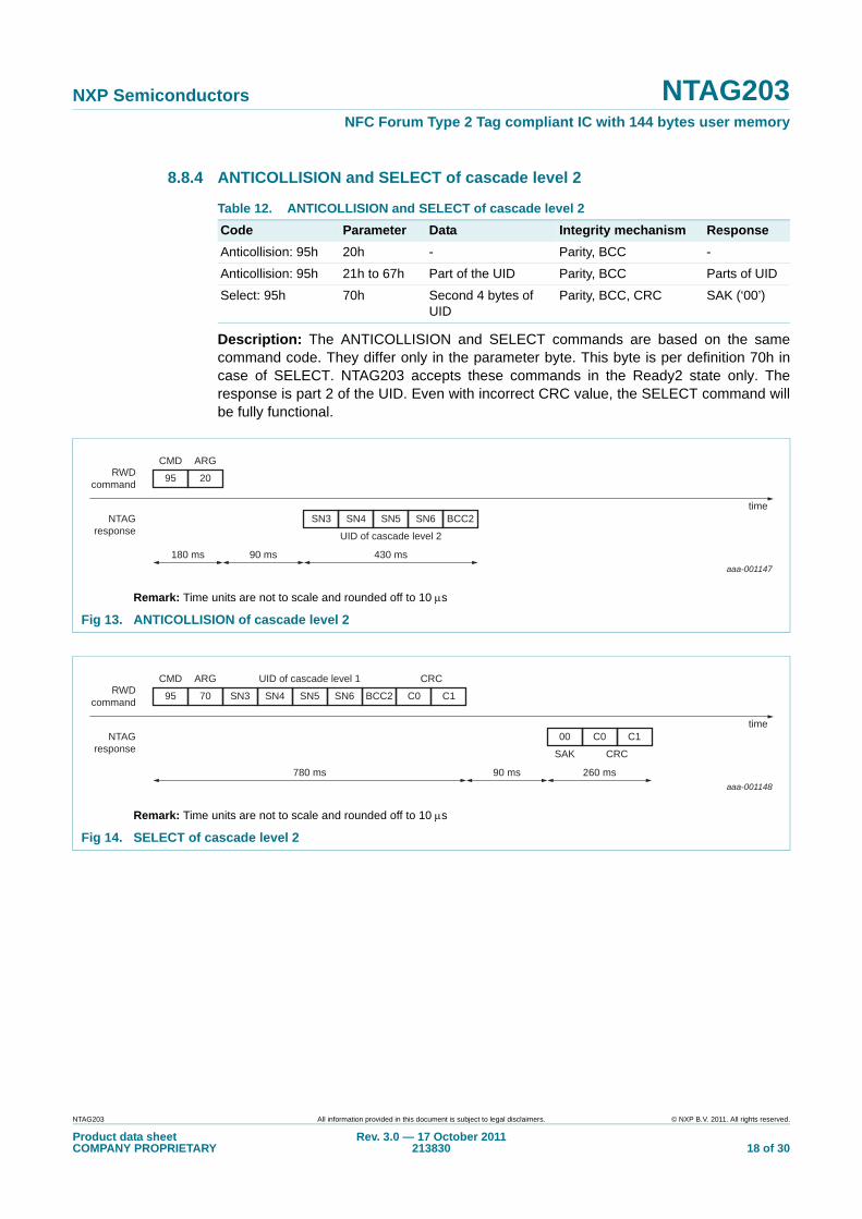
8.8.4 ANTICOLLISION and SELECT of cascade level 2
Description: The ANTICOLLISION and SELECT commands are based on the samecommand code. They differ only in the parameter byte. This byte is per definition 70h incase of SELECT. NTAG203 accepts these commands in the Ready2 state only. Theresponse is part 2 of the UID. Even with incorrect CRC value, the SELECT command willbe fully functional.
Table 12. ANTICOLLISION and SELECT of cascade level 2
Code Parameter Data Integrity mechanism Response
Anticollision: 95h 20h - Parity, BCC -
Anticollision: 95h 21h to 67h Part of the UID Parity, BCC Parts of UID
Select: 95h 70h Second 4 bytes of UID
Parity, BCC, CRC SAK (‘00’)
Remark: Time units are not to scale and rounded off to 10 s
Fig 13. ANTICOLLISION of cascade level 2
aaa-001147
CMD
180 ms
RWDcommand
timeNTAG
response
90 ms 430 ms
95
ARG
UID of cascade level 2
20
SN3 SN4 SN5 SN6 BCC2
Remark: Time units are not to scale and rounded off to 10 s
Fig 14. SELECT of cascade level 2
aaa-001148
CMD
780 ms
RWDcommand
timeNTAG
response
90 ms 260 ms
95
ARG CRC
SAK CRC
UID of cascade level 1
70 SN3 SN4 SN5 SN6 BCC2 C0 C1
00 C0 C1
NTAG203 All information provided in this document is subject to legal disclaimers. © NXP B.V. 2011. All rights reserved.
Product data sheetCOMPANY PROPRIETARY
Rev. 3.0 — 17 October 2011213830 18 of 30

NXP Semiconductors NTAG203NFC Forum Type 2 Tag compliant IC with 144 bytes user memory
8.8.5 READ
Description: The READ command needs the page address as a parameter. Onlyaddresses 00h to 29h are decoded. For higher addresses, NTAG203 returns a NAK. TheNTAG203 responds to the READ command by sending 16 bytes starting from the pageaddress defined in the command (e.g. if ADR is ‘03h‘ pages 03h, 04h, 05h, 06h arereturned. If ADR is ‘29h’, the contents of pages 29h, 00h, 01h and 02h is returned).
8.8.6 HALT
Description: The HALT command is used to set already processed NTAG203 devicesinto a different waiting state (Halt instead of Idle), which allows a simple separationbetween devices whose UIDs are already known (as they have already passed theanticollision procedure) and devices that have not yet been identified by their UIDs. Thismechanism is a very efficient way of finding all contactless devices in the field of a NFCdevice. Even with incorrect parity value, the HALT command will be fully functional.
Table 13. READ
Code Parameter/ARG Data Integrity mechanism Response
30h ADR: ‘00h’ to ‘29h‘ - Parity, CRC 16 Byte Date
Remark: Time units are not to scale and rounded off to 10 s
Fig 15. READ
aaa-001149
CMD
350 ms
RWDcommand
timeNTAG
response
90 ms
50 ms
1540 ms
30
ARG CRC
16 byte data CRC
ADR
NAK
C0 C1
D0 D1 D2 ... D13 D14 D15 C0 C1
Table 14. HALT
Code Parameter Data Integrity mechanism Response
50h 00h - Parity, CRC Passive ACK, NAK
Remark: Time units are not to scale and rounded off to 10 s
Fig 16. HALT
aaa-001150
CMD
350 ms
RWDcommand
timeNTAG
response
90 ms 50 ms
50
ADR CRC
00
NAK
C0 C1
- - -ACK
NTAG203 All information provided in this document is subject to legal disclaimers. © NXP B.V. 2011. All rights reserved.
Product data sheetCOMPANY PROPRIETARY
Rev. 3.0 — 17 October 2011213830 19 of 30
NXP Semiconductors NTAG203NFC Forum Type 2 Tag compliant IC with 144 bytes user memory
8.8.7 WRITE
Description: The WRITE command is used to program the lock bytes in page 02h, theOTP bytes in page 03h or the data bytes in pages 04h to 05h. A WRITE command isperformed page-wise, programming 4 bytes in a page.
Table 15. WRITE
Code Parameter/ARG Data Integrity mechanism Response
A2h ADR: ‘02h’ to ‘29h’ 4 Byte Parity, CRC ACK or NAK
Remark: Time units are not to scale and rounded off to 10 s
Fig 17. WRITE
aaa-001151
CMD
690 ms
RWDcommand
timeNTAG
response
90 ms
50 ms 50 ms
4110 ms
A2
ARG 4 byte data
ADR
NAK
D0 D1 D2
CRC
D3 C0 C1
AK
NTAG203 All information provided in this document is subject to legal disclaimers. © NXP B.V. 2011. All rights reserved.
Product data sheetCOMPANY PROPRIETARY
Rev. 3.0 — 17 October 2011213830 20 of 30

NXP Semiconductors NTAG203NFC Forum Type 2 Tag compliant IC with 144 bytes user memory
8.8.8 COMPATIBILITY WRITE
Description: The COMPATIBILITY WRITE command was implemented to accommodatethe established NFC device infrastructure. Even though 16 bytes are transferred to theNTAG203, only the least significant 4 bytes (bytes 0 to 3) will be written to the specifiedaddress. It is recommended to set the remaining bytes 4 to 15 to all ‘0’.
Table 16. COMPATIBILITY WRITE
Code Parameter/ARG Data Integrity mechanism Response
A0h ADR: ‘02h’ to ‘29h’ 16 Byte Parity, CRC ACK or NAK
Remark: Time units are not to scale and rounded off to 10 s
Fig 18. COMPATIBILITY WRITE
aaa-001152
CMD
350 ms
RWDcommand
timeNTAG
response
90 ms 1540 ms 90 ms
4110 ms
50 ms 50 ms
50 ms
A0
ARG CRC
ADR C0 C1
16 byte data
...
CRC
D15D0 C0 C1
NAK NAK
ACK
50 ms
ACK
NTAG203 All information provided in this document is subject to legal disclaimers. © NXP B.V. 2011. All rights reserved.
Product data sheetCOMPANY PROPRIETARY
Rev. 3.0 — 17 October 2011213830 21 of 30

NXP Semiconductors NTAG203NFC Forum Type 2 Tag compliant IC with 144 bytes user memory
8.9 Summary of relevant data for device identification
Table 17. Summary of relevant data for device identification
Code Type Value Binary Format Remark
ATQA 2 Byte 0044h 0000 0000 0100 0100
1st ‘1’ indicates cascade level 2
2nd ‘1’ indicates family
OK
CT 1 Byte
Cascade Tag
88h 1000 1000
ensures collision with cascade level 1 products
Hard Coded
SAK (casc. level 1) 1 Byte 04h 0000 0100
‘1’ indicates additional cascade level
OK
SAK (casc. level 2) 1 Byte 00h 0000 0000
indicates complete UID and NTAG203 functionality
OK
Manufacturer Byte 1 Byte 04h 0000 0100
indicates manufacturer NXP
Acc. toISO/IEC 14443-3 and ISO/IEC 7816-6 AMD.1
NTAG203 All information provided in this document is subject to legal disclaimers. © NXP B.V. 2011. All rights reserved.
Product data sheetCOMPANY PROPRIETARY
Rev. 3.0 — 17 October 2011213830 22 of 30

NXP Semiconductors NTAG203NFC Forum Type 2 Tag compliant IC with 144 bytes user memory
9. Limiting values
[1] Stresses above one or more of the limiting values may cause permanent damage to the device.
[2] Exposure to limiting values for extended periods may affect device reliability.
[3] MIL Standard 883-C method 3015; Human body model: C = 100 pF, R = 1.5 k.
10. Characteristics
10.1 Electrical characteristics
[1] Stresses above one or more of the limiting values may cause permanent damage to the device.
[2] These are stress ratings only. Operation of the device at these or any other conditions above those given in the Characteristics section of the specification is not implied.
[3] Exposure to limiting values for extended periods may affect device reliability.
[4] LCR meter HP 4285, Tamb = 22 C, Cp-D, fi = 13.56 MHz, 2Veff.
11. Package outline
This section is not applicable for this device.
Table 18. Limiting values In accordance with the Absolute Maximum Rating System (IEC 60134).[1][2]
Symbol Parameter Conditions Min Max Unit
II input current - 30 mA
Tstg storage temperature 55 +125 C
Tamb ambient temperature 25 +70 C
VESD electrostatic discharge voltage
measured on pin LA-LB
[3] 2 - kV
Table 19. CharacteristicsIn accordance with the Absolute Maximum Rating System (IEC 60134).[1][2][3]
Symbol Parameter Conditions Min Typ Max Unit
fi input frequency - 13.56 - MHz
Ci input capacitance 50 pF version (bare silicon and HWSON8)
[4] 44 50 56 pF
EEPROM characteristics
tcy(W) write cycle time - 4.1 - ms
tret retention time Tamb = 22 C 5 - - year
Nendu(W) write endurance Tamb = 22 C 10000 - - cycle
NTAG203 All information provided in this document is subject to legal disclaimers. © NXP B.V. 2011. All rights reserved.
Product data sheetCOMPANY PROPRIETARY
Rev. 3.0 — 17 October 2011213830 23 of 30
NXP Semiconductors NTAG203NFC Forum Type 2 Tag compliant IC with 144 bytes user memory
12. Abbreviations
13. References
[1] ISO/IEC — International Organization for Standardization/International Electrotechnical Commission
[2] Interface Platform Type Identification Procedure — Application note, BL-ID Doc. No.: 0184**2
[3] ISO/IEC 14443 PICC Selection — Application note, BL-ID Doc. No.: 1308**
[4] Ultralight Features and Hints — Application note, BL-ID Doc. No.: 0731**
[5] Ultralight as Type 2 Tag — Application note, BL-ID Doc. No.: 1303**
[6] (Card) Coil Design Guide — Application note, BL-ID Doc. No.: 0117**
[7] MF0ICU1 Functional specification MIFARE Ultralight — Product data sheet, BL-ID Doc. No. 0286**
[8] NIST SP800-67: Recommendation for the Triple Data Encryption Algorithm (TDEA) Block Cipher, Version 1.1 May 19, 2008 — National Institute of Standards and Technology
Table 20. Abbreviations
Acronym Description
ACK positive ACKnowledge
ATQA Answer To reQuest, type A
BCC Block Check Characters byte
CBC Cipher-Block Chaining
CRC Cyclic Redundancy Check
CT Cascade Tag, Type A
EEPROM Electrically Erasable Programmable Read-Only Memory
IV Initial Value
MSB Most Significant Bit
NAK Negative AcKnowledge
LSB Least Significant Bit
OTP One Time Programmable
Passive ACK Implicit acknowledge without PICC answer
PCD Proximity Coupling Device
PICC Proximity Integrated Circuit Card
POR Power On Reset
REQA ReQuest Answer, type A
RF Radio Frequency
SAK Select AcKnowledge, type A
UID Unique IDentifier
WUPA Wake-UP command, type A
2. ** ... document version number
NTAG203 All information provided in this document is subject to legal disclaimers. © NXP B.V. 2011. All rights reserved.
Product data sheetCOMPANY PROPRIETARY
Rev. 3.0 — 17 October 2011213830 24 of 30
NXP Semiconductors NTAG203NFC Forum Type 2 Tag compliant IC with 144 bytes user memory
[9] ISO/IEC 10116: Information technology - Security techniques - Modes of operation for an n-bit block cipher, February 1, 2006 — International Organization for Standardization
[10] Tag 2 Type Operation, Technical Specification — NFC Forum, 09.07.2007
[11] NFC Data Exchange Format (NDEF), Technical Specification — NFC Forum, 24.07.2006
[12] NXP Semiconductors guidance for soldering the HWSON8 package; URL: http://www.nxp.com/#/page/content=[f=/packages/SOT1069-2.xml] — NXP Semiconductors, 21.08.2009
NTAG203 All information provided in this document is subject to legal disclaimers. © NXP B.V. 2011. All rights reserved.
Product data sheetCOMPANY PROPRIETARY
Rev. 3.0 — 17 October 2011213830 25 of 30

NXP Semiconductors NTAG203NFC Forum Type 2 Tag compliant IC with 144 bytes user memory
14. Revision history
Table 21. Revision history
Document ID Release date Data sheet status Change notice Supersedes
NTAG203 v.3.0 20111017 Product data sheet - -
NTAG203 All information provided in this document is subject to legal disclaimers. © NXP B.V. 2011. All rights reserved.
Product data sheetCOMPANY PROPRIETARY
Rev. 3.0 — 17 October 2011213830 26 of 30
NXP Semiconductors NTAG203NFC Forum Type 2 Tag compliant IC with 144 bytes user memory
15. Legal information
15.1 Data sheet status
[1] Please consult the most recently issued document before initiating or completing a design.
[2] The term ‘short data sheet’ is explained in section “Definitions”.
[3] The product status of device(s) described in this document may have changed since this document was published and may differ in case of multiple devices. The latest product status information is available on the Internet at URL http://www.nxp.com.
15.2 Definitions
Draft — The document is a draft version only. The content is still under internal review and subject to formal approval, which may result in modifications or additions. NXP Semiconductors does not give any representations or warranties as to the accuracy or completeness of information included herein and shall have no liability for the consequences of use of such information.
Short data sheet — A short data sheet is an extract from a full data sheet with the same product type number(s) and title. A short data sheet is intended for quick reference only and should not be relied upon to contain detailed and full information. For detailed and full information see the relevant full data sheet, which is available on request via the local NXP Semiconductors sales office. In case of any inconsistency or conflict with the short data sheet, the full data sheet shall prevail.
Product specification — The information and data provided in a Product data sheet shall define the specification of the product as agreed between NXP Semiconductors and its customer, unless NXP Semiconductors and customer have explicitly agreed otherwise in writing. In no event however, shall an agreement be valid in which the NXP Semiconductors product is deemed to offer functions and qualities beyond those described in the Product data sheet.
15.3 Disclaimers
Limited warranty and liability — Information in this document is believed to be accurate and reliable. However, NXP Semiconductors does not give any representations or warranties, expressed or implied, as to the accuracy or completeness of such information and shall have no liability for the consequences of use of such information.
In no event shall NXP Semiconductors be liable for any indirect, incidental, punitive, special or consequential damages (including - without limitation - lost profits, lost savings, business interruption, costs related to the removal or replacement of any products or rework charges) whether or not such damages are based on tort (including negligence), warranty, breach of contract or any other legal theory.
Notwithstanding any damages that customer might incur for any reason whatsoever, NXP Semiconductors’ aggregate and cumulative liability towards customer for the products described herein shall be limited in accordance with the Terms and conditions of commercial sale of NXP Semiconductors.
Right to make changes — NXP Semiconductors reserves the right to make changes to information published in this document, including without limitation specifications and product descriptions, at any time and without notice. This document supersedes and replaces all information supplied prior to the publication hereof.
Suitability for use — NXP Semiconductors products are not designed, authorized or warranted to be suitable for use in life support, life-critical or safety-critical systems or equipment, nor in applications where failure or
malfunction of an NXP Semiconductors product can reasonably be expected to result in personal injury, death or severe property or environmental damage. NXP Semiconductors accepts no liability for inclusion and/or use of NXP Semiconductors products in such equipment or applications and therefore such inclusion and/or use is at the customer’s own risk.
Applications — Applications that are described herein for any of these products are for illustrative purposes only. NXP Semiconductors makes no representation or warranty that such applications will be suitable for the specified use without further testing or modification.
Customers are responsible for the design and operation of their applications and products using NXP Semiconductors products, and NXP Semiconductors accepts no liability for any assistance with applications or customer product design. It is customer’s sole responsibility to determine whether the NXP Semiconductors product is suitable and fit for the customer’s applications and products planned, as well as for the planned application and use of customer’s third party customer(s). Customers should provide appropriate design and operating safeguards to minimize the risks associated with their applications and products.
NXP Semiconductors does not accept any liability related to any default, damage, costs or problem which is based on any weakness or default in the customer’s applications or products, or the application or use by customer’s third party customer(s). Customer is responsible for doing all necessary testing for the customer’s applications and products using NXP Semiconductors products in order to avoid a default of the applications and the products or of the application or use by customer’s third party customer(s). NXP does not accept any liability in this respect.
Limiting values — Stress above one or more limiting values (as defined in the Absolute Maximum Ratings System of IEC 60134) will cause permanent damage to the device. Limiting values are stress ratings only and (proper) operation of the device at these or any other conditions above those given in the Recommended operating conditions section (if present) or the Characteristics sections of this document is not warranted. Constant or repeated exposure to limiting values will permanently and irreversibly affect the quality and reliability of the device.
Terms and conditions of commercial sale — NXP Semiconductors products are sold subject to the general terms and conditions of commercial sale, as published at http://www.nxp.com/profile/terms, unless otherwise agreed in a valid written individual agreement. In case an individual agreement is concluded only the terms and conditions of the respective agreement shall apply. NXP Semiconductors hereby expressly objects to applying the customer’s general terms and conditions with regard to the purchase of NXP Semiconductors products by customer.
No offer to sell or license — Nothing in this document may be interpreted or construed as an offer to sell products that is open for acceptance or the grant, conveyance or implication of any license under any copyrights, patents or other industrial or intellectual property rights.
Export control — This document as well as the item(s) described herein may be subject to export control regulations. Export might require a prior authorization from competent authorities.
Document status[1][2] Product status[3] Definition
Objective [short] data sheet Development This document contains data from the objective specification for product development.
Preliminary [short] data sheet Qualification This document contains data from the preliminary specification.
Product [short] data sheet Production This document contains the product specification.
NTAG203 All information provided in this document is subject to legal disclaimers. © NXP B.V. 2011. All rights reserved.
Product data sheetCOMPANY PROPRIETARY
Rev. 3.0 — 17 October 2011213830 27 of 30
NXP Semiconductors NTAG203NFC Forum Type 2 Tag compliant IC with 144 bytes user memory
Quick reference data — The Quick reference data is an extract of the product data given in the Limiting values and Characteristics sections of this document, and as such is not complete, exhaustive or legally binding.
Non-automotive qualified products — Unless this data sheet expressly states that this specific NXP Semiconductors product is automotive qualified, the product is not suitable for automotive use. It is neither qualified nor tested in accordance with automotive testing or application requirements. NXP Semiconductors accepts no liability for inclusion and/or use of non-automotive qualified products in automotive equipment or applications.
In the event that customer uses the product for design-in and use in automotive applications to automotive specifications and standards, customer (a) shall use the product without NXP Semiconductors’ warranty of the product for such automotive applications, use and specifications, and (b) whenever customer uses the product for automotive applications beyond NXP Semiconductors’ specifications such use shall be solely at customer’s own risk, and (c) customer fully indemnifies NXP Semiconductors for any liability, damages or failed product claims resulting from customer design and use of the product for automotive applications beyond NXP Semiconductors’ standard warranty and NXP Semiconductors’ product specifications.
15.4 Licenses
15.5 TrademarksNotice: All referenced brands, product names, service names and trademarks are the property of their respective owners.
MIFARE — is a trademark of NXP B.V.
MIFARE Ultralight — is a trademark of NXP B.V.
16. Contact information
For more information, please visit: http://www.nxp.com
For sales office addresses, please send an email to: [email protected]
Purchase of NXP ICs with NFC technology
Purchase of an NXP Semiconductors IC that complies with one of the Near Field Communication (NFC) standards ISO/IEC 18092 and ISO/IEC 21481 does not convey an implied license under any patent right infringed by implementation of any of those standards. A license for the patents portfolio of NXP B.V. for the NFC standards needs to be obtained at Via Licensing, the pool agent of the NFC Patent Pool, e-mail: [email protected].
NTAG203 All information provided in this document is subject to legal disclaimers. © NXP B.V. 2011. All rights reserved.
Product data sheetCOMPANY PROPRIETARY
Rev. 3.0 — 17 October 2011213830 28 of 30
NXP Semiconductors NTAG203NFC Forum Type 2 Tag compliant IC with 144 bytes user memory
17. Tables
Table 1. Short naming convention (for easier product identification) . . . . . . . . . . . . . . . . . . . . . . . . . . .2
Table 2. Ordering information. . . . . . . . . . . . . . . . . . . . . .3Table 3. Bonding pad assignments to smart card
contactless module . . . . . . . . . . . . . . . . . . . . . . .4Table 4. Wafer specifications . . . . . . . . . . . . . . . . . . . . . .5Table 5. Memory organization . . . . . . . . . . . . . . . . . . . .10Table 6. Lock bytes . . . . . . . . . . . . . . . . . . . . . . . . . . . . 11Table 7. Initial memory organization . . . . . . . . . . . . . . .14Table 8. ACK and NAK values . . . . . . . . . . . . . . . . . . . .15Table 9. REQA . . . . . . . . . . . . . . . . . . . . . . . . . . . . . . . .16Table 10. WUPA . . . . . . . . . . . . . . . . . . . . . . . . . . . . . . . .16Table 11. ANTICOLLISION and SELECT of
cascade level 1 . . . . . . . . . . . . . . . . . . . . . . . . 17Table 12. ANTICOLLISION and SELECT
of cascade level 2 . . . . . . . . . . . . . . . . . . . . . . 18Table 13. READ . . . . . . . . . . . . . . . . . . . . . . . . . . . . . . . . 19Table 14. HALT . . . . . . . . . . . . . . . . . . . . . . . . . . . . . . . . 19Table 15. WRITE . . . . . . . . . . . . . . . . . . . . . . . . . . . . . . . 20Table 16. COMPATIBILITY WRITE . . . . . . . . . . . . . . . . . 21Table 17. Summary of relevant data for device
identification . . . . . . . . . . . . . . . . . . . . . . . . . . . 22Table 18. Limiting values . . . . . . . . . . . . . . . . . . . . . . . . 23Table 19. Characteristics . . . . . . . . . . . . . . . . . . . . . . . . 23Table 20. Abbreviations . . . . . . . . . . . . . . . . . . . . . . . . . . 24Table 21. Revision history . . . . . . . . . . . . . . . . . . . . . . . . 26
18. Figures
Fig 1. NFC Tag interacting with NFC enabled device . . .1Fig 2. Block diagram . . . . . . . . . . . . . . . . . . . . . . . . . . . .3Fig 3. Chip orientation and bond pad locations . . . . . . . .4Fig 4. Communication principle state
diagram - 4-byte; 16-byte. . . . . . . . . . . . . . . . . . . .7Fig 5. UID/serial number . . . . . . . . . . . . . . . . . . . . . . . .10Fig 6. Lock bytes 1 and 2. . . . . . . . . . . . . . . . . . . . . . . .12Fig 7. Lock bytes 3 and 4. . . . . . . . . . . . . . . . . . . . . . . .12Fig 8. OTP bytes . . . . . . . . . . . . . . . . . . . . . . . . . . . . . .13Fig 9. REQA. . . . . . . . . . . . . . . . . . . . . . . . . . . . . . . . . .16Fig 10. WUPA . . . . . . . . . . . . . . . . . . . . . . . . . . . . . . . . .16Fig 11. ANTICOLLISION of cascade level 1 . . . . . . . . . .17Fig 12. SELECT of cascade level 1 . . . . . . . . . . . . . . . . .17Fig 13. ANTICOLLISION of cascade level 2 . . . . . . . . . .18Fig 14. SELECT of cascade level 2 . . . . . . . . . . . . . . . . .18Fig 15. READ. . . . . . . . . . . . . . . . . . . . . . . . . . . . . . . . . .19Fig 16. HALT . . . . . . . . . . . . . . . . . . . . . . . . . . . . . . . . . .19Fig 17. WRITE . . . . . . . . . . . . . . . . . . . . . . . . . . . . . . . . .20Fig 18. COMPATIBILITY WRITE . . . . . . . . . . . . . . . . . . .21
NTAG203 All information provided in this document is subject to legal disclaimers. © NXP B.V. 2011. All rights reserved.
Product data sheetCOMPANY PROPRIETARY
Rev. 3.0 — 17 October 2011213830 29 of 30

NXP Semiconductors NTAG203NFC Forum Type 2 Tag compliant IC with 144 bytes user memory
19. Contents
1 General description . . . . . . . . . . . . . . . . . . . . . . 11.1 Contactless energy and data transfer. . . . . . . . 11.2 Naming conventions . . . . . . . . . . . . . . . . . . . . . 2
2 Features and benefits . . . . . . . . . . . . . . . . . . . . 22.1 RF Interface (ISO/IEC 14443A) . . . . . . . . . . . . 22.2 EEPROM . . . . . . . . . . . . . . . . . . . . . . . . . . . . . 22.3 NFC Forum Tag 2 Type compliance . . . . . . . . . 22.4 Security. . . . . . . . . . . . . . . . . . . . . . . . . . . . . . . 22.5 Cascaded UID . . . . . . . . . . . . . . . . . . . . . . . . . 32.6 Anticollision. . . . . . . . . . . . . . . . . . . . . . . . . . . . 3
3 Ordering information. . . . . . . . . . . . . . . . . . . . . 3
4 Block diagram . . . . . . . . . . . . . . . . . . . . . . . . . . 3
5 Pinning information. . . . . . . . . . . . . . . . . . . . . . 35.1 Pin description . . . . . . . . . . . . . . . . . . . . . . . . . 3
6 Wafer layout . . . . . . . . . . . . . . . . . . . . . . . . . . . . 4
7 Mechanical specification . . . . . . . . . . . . . . . . . 57.1 Fail die identification . . . . . . . . . . . . . . . . . . . . . 6
8 Functional description . . . . . . . . . . . . . . . . . . . 68.1 Block description . . . . . . . . . . . . . . . . . . . . . . . 68.2 State diagram and logical states description . . 78.2.1 Idle state . . . . . . . . . . . . . . . . . . . . . . . . . . . . . . 88.2.2 Ready1 state. . . . . . . . . . . . . . . . . . . . . . . . . . . 88.2.3 Ready2 state. . . . . . . . . . . . . . . . . . . . . . . . . . . 88.2.4 Active state . . . . . . . . . . . . . . . . . . . . . . . . . . . . 88.2.5 Halt state. . . . . . . . . . . . . . . . . . . . . . . . . . . . . . 98.3 Data integrity. . . . . . . . . . . . . . . . . . . . . . . . . . . 98.4 RF interface . . . . . . . . . . . . . . . . . . . . . . . . . . . 98.5 Memory organization . . . . . . . . . . . . . . . . . . . 108.5.1 UID/serial number. . . . . . . . . . . . . . . . . . . . . . 108.5.2 Lock bytes . . . . . . . . . . . . . . . . . . . . . . . . . . . 118.5.3 OTP bytes. . . . . . . . . . . . . . . . . . . . . . . . . . . . 138.5.4 Data pages . . . . . . . . . . . . . . . . . . . . . . . . . . . 138.5.5 Initial memory configuration . . . . . . . . . . . . . . 148.6 Counter . . . . . . . . . . . . . . . . . . . . . . . . . . . . . . 158.7 PICC response to a command from
NFC device. . . . . . . . . . . . . . . . . . . . . . . . . . . 158.8 Command set . . . . . . . . . . . . . . . . . . . . . . . . . 168.8.1 REQA . . . . . . . . . . . . . . . . . . . . . . . . . . . . . . . 168.8.2 WUPA . . . . . . . . . . . . . . . . . . . . . . . . . . . . . . . 168.8.3 ANTICOLLISION and SELECT of
cascade level 1. . . . . . . . . . . . . . . . . . . . . . . . 178.8.4 ANTICOLLISION and SELECT of
cascade level 2. . . . . . . . . . . . . . . . . . . . . . . . 188.8.5 READ . . . . . . . . . . . . . . . . . . . . . . . . . . . . . . . 198.8.6 HALT. . . . . . . . . . . . . . . . . . . . . . . . . . . . . . . . 198.8.7 WRITE . . . . . . . . . . . . . . . . . . . . . . . . . . . . . . 20
8.8.8 COMPATIBILITY WRITE . . . . . . . . . . . . . . . . 218.9 Summary of relevant data for device
identification . . . . . . . . . . . . . . . . . . . . . . . . . . 22
9 Limiting values . . . . . . . . . . . . . . . . . . . . . . . . 23
10 Characteristics . . . . . . . . . . . . . . . . . . . . . . . . 2310.1 Electrical characteristics . . . . . . . . . . . . . . . . 23
11 Package outline. . . . . . . . . . . . . . . . . . . . . . . . 23
12 Abbreviations . . . . . . . . . . . . . . . . . . . . . . . . . 24
13 References. . . . . . . . . . . . . . . . . . . . . . . . . . . . 24
14 Revision history . . . . . . . . . . . . . . . . . . . . . . . 26
15 Legal information . . . . . . . . . . . . . . . . . . . . . . 2715.1 Data sheet status . . . . . . . . . . . . . . . . . . . . . . 2715.2 Definitions . . . . . . . . . . . . . . . . . . . . . . . . . . . 2715.3 Disclaimers . . . . . . . . . . . . . . . . . . . . . . . . . . 2715.4 Licenses. . . . . . . . . . . . . . . . . . . . . . . . . . . . . 2815.5 Trademarks . . . . . . . . . . . . . . . . . . . . . . . . . . 28
16 Contact information . . . . . . . . . . . . . . . . . . . . 28
17 Tables . . . . . . . . . . . . . . . . . . . . . . . . . . . . . . . . 29
18 Figures . . . . . . . . . . . . . . . . . . . . . . . . . . . . . . . 29
19 Contents. . . . . . . . . . . . . . . . . . . . . . . . . . . . . . 30
© NXP B.V. 2011. All rights reserved.
For more information, please visit: http://www.nxp.comFor sales office addresses, please send an email to: [email protected]
Date of release: 17 October 2011213830
Please be aware that important notices concerning this document and the product(s)described herein, have been included in section ‘Legal information’.