ntsc/pal/secam video decoder with component input and ... · tw9912 5 introduction the tw9912 is a...
TRANSCRIPT

1
FN7945.1
September 27, 2012
CAUTION: These devices are sensitive to electrostatic discharge; follow proper IC Handling Procedures.
1-888-INTERSIL or 1-888-468-3774 | Copyright Intersil Americas Inc. 2012. All Rights Reserved
Intersil (and design) is a trademark owned by Intersil Corporation or one of its subsidiaries.
All other trademarks mentioned are the property of their respective owners.
T e c h w e l l
NTSC/PAL/SECAM Video Decoder with Component Input and Progressive Output Support
TW9912
Features
Video Decoder
NTSC (M, 4.43) and PAL (B, D, G, H, I, M, N, N
combination), PAL (60), SECAM support with
automatic format detection
Software selectable analog input control
Built-in analog anti-alias filter
Fully programmable static gain or automatic gain
control for the Y channel
Programmable white peak control for the Y channel
4-H adaptive comb filter Y/C separation
PAL delay line for color phase error correction
Image enhancement with peaking and CTI
Digital sub-carrier PLL for accurate color decoding
Digital Horizontal PLL for synchronization processing
and pixel sampling
Advanced synchronization processing and sync
detection for handling non-standard and weak signal
Programmable hue, brightness, saturation, contrast,
and sharpness
Automatic color control and color killer
Chroma IF compensation
VBI slicer supporting CC and WSS data services
Programmable output control
Analog Video Input
Triple 10-bit ADCs with independent clamping and
gain control
Supports 480i/480p/576i/576p analog component
input with SOG
Digital Output
ITU-R 656 compatible YCbCr(4:2:2) output format
Progressive ITU-R 656 output format support for both
interlaced and progressive inputs
Miscellaneous
Two wire MPU serial bus interface
Power save and Power down mode
Low power consumption
Single 27MHz crystal for all operations
3.3V tolerant I/O
1.8V/3.3 V power supply
48 pin QFN package

TW9912
2
Functional Description
Ordering Information
PART
NUMBER
PART
MARKING
PACKAGE
(Pb-free)
PKG.
DWG. #
TW9912-NA3-CR
(Note 1) TW9912 NA3-CR 48 Ld QFN L48.7X7L
NOTE:
1. These Intersil Pb-free plastic packaged products employ special Pb-free material sets, molding compounds/die attach
materials, and 100% matte tin plate plus anneal (e3 termination finish, which is RoHS compliant and compatible with both
SnPb and Pb-free soldering operations). Intersil Pb-free products are MSL classified at Pb-free peak reflow temperatures that
meet or exceed the Pb-free requirements of IPC/JEDEC J STD-020.
FIGURE 1. TW9912 BLOCK DIAGRAM
RSTB
SOG
Com
ponent
Pro
cessin
g
Analo
g V
ideo In
Triple
10-b
it A
FE
4H
Adaptiv
e
Com
b F
ilter C
hro
ma
Dem
odula
tion
Lum
a/C
hro
ma
pro
cessin
g
Sync
Pro
cessor
Vid
eo Inte
rface
VB
I S
licer
2 W
ire
Serial B
us
CIN1-0
YIN3-0
MPOUT
CLKO
VSO
HSO
VD[7:0]
VIN 0
SCLK
SDAT
U
V
PLL
PDN
Clo
ck
27 Mhz
Y
Lin
e-lock
clo
ck
Genera
tor

TW9912
3
Table of Contents Ordering Information .................................................................. 2 Functional Description ............................................................... 2
Introduction ............................................................................... 5 Analog Front End ..................................................................... 5 Sync Processor ........................................................................ 5 Y/C Separation ......................................................................... 5 Color Demodulation ................................................................. 5
Automatic Chroma Gain Control .......................................... 6 Color Killer ............................................................................ 6 Automatic standard detection .............................................. 6
Component Processing ........................................................... 7 Sharpness............................................................................. 7 Color Transient Improvement .............................................. 7
Power Management ................................................................ 7 Host Interface ........................................................................... 7 Cropping ................................................................................... 8 Output Interface ....................................................................... 9
ITU-R BT.656 ....................................................................... 9 Control Signals ..................................................................... 9 Vertical timing diagram ......................................................... 9 HSYNC ...............................................................................12 VSYNC ...............................................................................12 FIELD ..................................................................................12
Closed Captioning and Extended Data Services .................12 Two Wire Serial Bus Interface ...............................................14 Filter Curves ...........................................................................16
Anti-alias filter .....................................................................16 Decimation filter ..................................................................16 Chroma Band Pass Filter Curves ......................................17 Luma Notch Filter Curve for NTSC and PAL/SECAM ......17 Chrominance Low-Pass Filter Curve .................................18 Peaking Filter Curves .........................................................19
Pin Diagram ...............................................................................20 48 Pin QFN ............................................................................20 Pin Descriptions .....................................................................21
Power and Ground Pins .....................................................22 Parametric Information ............................................................23
AC/DC Electrical Parameters ................................................23 Output Timing .....................................................................26 Serial Host Interface Timing ...............................................27 Serial Host Interface Timing Diagram ................................27
Package Outline Drawing ........................................................28 Application Schematics..........................................................29
PCB Layout Considerations ...............................................30 Thermal Pad Consideration ...............................................31
TW9912 Register Summary .....................................................32 ADC/LLPLL .........................................................................34 0x01 – Chip Status Register (CSTATUS) .........................36 0x02 – Input Format (INFORM) .........................................36 0x03 – Output Control Register (OPFORM) .....................37 0x04 – Color Killer Hysteresis and HSYNC Delay Control38 0x05 – Output Control Register II ......................................38 0x06 – Analog Control Register (ACNTL) .........................39 0x07 – Cropping Register, High (CROP_HI) ....................40 0x08 – Vertical Delay Register, Low (VDELAY_LO) ........40 0x09 – Vertical Active Register, Low (VACTIVE_LO).......40 0x0A – Horizontal Delay Register, Low (HDELAY_LO) ...40 0x0B – Horizontal Active Register, Low (HACTIVE_LO)..41 0x0C – Control Register I (CNTRL1) .................................41 0x0D – CC/WSS Control....................................................41 0x10 – BRIGHTNESS Control Register (BRIGHT) ..........42 0x11 – CONTRAST Control Register (CONTRAST) .......42 0x12 – SHARPNESS Control Register I (SHARPNESS) 42 0x13 – Chroma (U) Gain Register (SAT_U) .....................43 0x14 – Chroma (V) Gain Register (SAT_V) ......................43 0x15 – Hue Control Register (HUE) ..................................43 0x16 – Reserved ................................................................43
0x17 – Vertical Peaking Control I ...................................... 44 0x18 – Coring Control Register (CORING) ...................... 44 0x19 – Reserved ................................................................ 44 0x1A – CC/EDS Status Register (CC_STATUS) ............. 45 0x1B – CC/EDS Data Register (CC_DATA) .................... 45 0x1C – Standard Selection (SDT) ..................................... 46 0x1D – Standard Recognition (SDTR) .............................. 46 0x1E – Component Video Format (CVFMT) .................... 47 0x1F – Reserved ............................................................... 47 0x20 – Clamping Gain (CLMPG) ...................................... 47 0x21 – Individual AGC Gain (IAGC) ................................. 47 0x22 – AGC Gain (AGCGAIN) .......................................... 48 0x23 – White Peak Threshold (PEAKWT) ........................ 48 0x24– Clamp level (CLMPL) ............................................. 48 0x25– Sync Amplitude (SYNCT) ....................................... 48 0x26 – Sync Miss Count Register (MISSCNT) ................. 48 0x27 – Clamp Position Register (PCLAMP) ..................... 49 0x28 – Vertical Control I .................................................... 49 0x29 – Vertical Control II ................................................... 49 0x2A – Color Killer Level Control ...................................... 50 0x2B – Comb Filter Control ............................................... 50 0x2C – Luma Delay and HFilter Control ........................... 50 0x2D – Miscellaneous Control Register I (MISC1) ........... 50 0x2E – Miscellaneous Control Register II (MISC2) .......... 51 0x2F – Miscellaneous Control III (MISC3) ........................ 52 0x30 – Copy Protection Detection ..................................... 52 0x31 – Chip STATUS II (CSTATUS2) .............................. 53 0x32 – H Monitor (HFREF) ................................................ 53 0x33 – CLAMP MODE(CLMD) ......................................... 54 0x34 – ID Detection Control (NSEN/SSEN/PSEN/WKTH)54 0x35 – Clamp Control (CLCNTL) ...................................... 55 0x36 – De-interlacer Control .............................................. 55 0x37 – De-interlacer H Delay Control ............................... 55 0x38 – De-interlacer Sync Generation .............................. 56 0x40 – WSS0 ..................................................................... 56 0x41 – WSS1 ..................................................................... 56 0x42 – WSS2 ..................................................................... 56 0x43 – CCEVENLINE ........................................................ 56 ADC/PLL Configuration Registers..................................... 57 0xC0 – LLPLL Input Control Register ............................... 57 0xC1 – LLPLL Input Detection Register ........................... 57 0xC2 – LLPLL Control Register ........................................ 58 0xC3 – LLPLL Divider High Register ................................ 58 0xC4 – LLPLL Divider Low Register ................................. 58 0xC5 – LLPLL Clock Phase Register ............................... 58 0xC6 – LLPLL Loop Control Register ............................... 59 0xC7 – LLPLL VCO Control Register ............................... 59 0xC8 – LLPLL VCO Control Register ............................... 59 0xC9 – LLPLL Pre Coast Register .................................... 59 0xCA – LLPLL Post Coast Register .................................. 59 0xCB – SOG Threshold Register ...................................... 60 0xCC – Scaler Sync Selection Register ........................... 60 0xCD – PLL Initialization Register ..................................... 61 0xD0 –Gain Control Register ............................................ 61 0xD1 – Y Channel Gain Adjust Register ........................... 61 0xD2 – C Channel Gain Adjust Register .......................... 61 0xD3 – V Channel Gain Adjust Register ........................... 61 0xD4 – Clamp Mode Control Register .............................. 62 0xD5 – Clamp Start Position Register .............................. 62 0xD6 – Clamp Stop Position Register............................... 62 0xD7 – Clamp Master Location Register .......................... 62 0xD8 – ADC TEST Register .............................................. 63 0xD9 – Y Clamp Reference Register ................................ 63 0xDA – C Clamp Reference Register ............................... 63 0xDB – V Clamp Reference Register ............................... 63 0xDC – HSO Width ............................................................ 63 0xE0 – LLPLL Control Register ......................................... 64 0xE1 – GPLL Control Register .......................................... 64 0xE2 – ADC Control I ........................................................ 65 0xE6 – ADC Control V ....................................................... 65

TW9912
4
0xE7 – ADC Control VI ......................................................66 0xE8 – ADC Control VII .....................................................66 0xE9 – Clock Control..........................................................67
Life Support Policy ...................................................................68
Datasheet Revision History .................................................... 68

TW9912
5
Introduction
The TW9912 is a low power NTSC/PAL/SECAM video decoder chip that also supports analog component
video as an input. The video decoder decodes the base-band analog CVBS or S-video signals into digital an
8-bit 4:2:2 YCbCr format. The analog component video is digitized into an 8-bit YCbCr format. The digital
output supports standard BT.656 format for interlaced video. It can also output progressive BT.656 format
when receiving a progressive component input or by converting interlaced video into progressive format via
an internal de-interlacing engine. TW9912 uses the 1.8V for both analog and digital supply voltage and 3.3V
for I/O power. A single 27MHz crystal is all that needed to decode all analog video standards.
This chip consists of an analog front-end with input source selection, a variable gain amplifier, analog-to-
digital converters, a Y/C separation circuit, a multi-standard color decoder (PAL BGHI, PAL M, PAL N,
combination PAL N, NTSC M, NTSC 4.43 and SECAM) and synchronization circuitry. Y/C separation is done
with a high quality adaptive 4H comb filter for reduced cross color and cross luminance. The advanced
synchronization processing circuitry can produce stable pictures for non-standard and weak signals. The
output of the decoder is line-locked to its inputs.
TW9912 also includes circuits to detect and process vertical blanking interval (VBI) signals, including closed
caption and WSS. It slices and process VBI data for output by register readout through the host interface. It
also detects analog copy-protected signals that contains AGC and colorstripe pulses.
A 2-wire serial host interface is used to simplify system integration. All the functions can be controlled
through this interface.
Analog Front End
The analog front-end pre-processes and digitizes the AC coupled analog signal for further processing. All
channels have built-in anti-aliasing filters and 10-bit high speed ADCs. The characteristics of the filter is
available in the filter curve section of this datasheet. All channels have built-in variable gain amplifier that
can be programmed. The Y channel gain can be automatically controlled in the decoder mode if enabled. It
can support a maximum input voltage range of 1.4V without attenuation. All channels also have a clamping
circuit that restores the proper DC level through manual or automatic control.
Sync Processor
The sync processor of TW9912 detects horizontal synchronization and vertical synchronization signals in the
composite video or in the Y signal of an S-video or component input. The processor contains a digital phase-
locked-loop and decision logic to achieve reliable sync detection in a stable signal as well as in an unstable
signal, such as those from VCR fast forward or rewind. It allows the sampling of the video signal in line-locked
fashion. In the case of progressive component input, the SOG input is used to control the sync processor PLL
for sampling the input video.
Y/C Separation
For NTSC and PAL standard signals in decoder mode, the luma/chroma separation can be done either by
adaptive comb filtering or notch/band-pass filter combination. For SECAM standard signals, only notch/band-
pass filter is available. The default selection for NTSC/PAL is comb filter. The characteristics of the band-pass
filter are shown in the filter curve section.
TW9912 employs high quality 4-H adaptive comb filter to reduce artifacts like hanging dots and crawling
dots. Due to the line buffer used in the comb filter, there is always a two line processing delay in the output
images no matter what standard or filter option is chosen.
Color Demodulation
The color demodulation of NTSC and PAL signal is done by first quadrature down mixing and then low-pass
filtering. The low-pass filter characteristic can be selected for optimized transient color performance. For the
PAL system, the PAL ID or the burst phase switching is identified to aid the PAL color demodulation.

TW9912
6
The SECAM decoding process consists of FM demodulator and de-emphasis filtering. During the FM
demodulation, the chroma carrier frequency is identified and used to control the SECAM color demodulation.
The sub-carrier signal for use in the color demodulator is generated by direct digital synthesis PLL that locks
onto the input sub-carrier reference (color burst). This arrangement allows any sub-standard of NTSC and PAL
to be demodulated easily with single crystal frequency.
AUTOMATIC CHROMA GAIN CONTROL
The Automatic Chroma Gain Control (ACC) compensates for reduced amplitudes caused by high-frequency
loss in video signal. The range of ACC control is –6db to +26db.
COLOR KILLER
For low color amplitude signals, black and white video, or very noisy signals, the color will be ―killed‖.
TW9912‘s color killer uses the burst amplitude measurement as well as sub-carrier PLL status to switch-off
the color.
AUTOMATIC STANDARD DETECTION
The TW9912 has build-in automatic standard discrimination circuitry. The circuit uses burst-phase, burst-
frequency and frame rate to identify NTSC, PAL or SECAM color signals. The standards that can be identified
are NTSC (M), NTSC (4.43), PAL (B, D, G, H, I), PAL (M), PAL (N), PAL (60) and SECAM (M). Each standard can
be included or excluded in the standard recognition process by software control. The identified standard is
indicated by the Standard Selection (SDT) register. Automatic standard detection can be overridden by
software controlled standard selection.
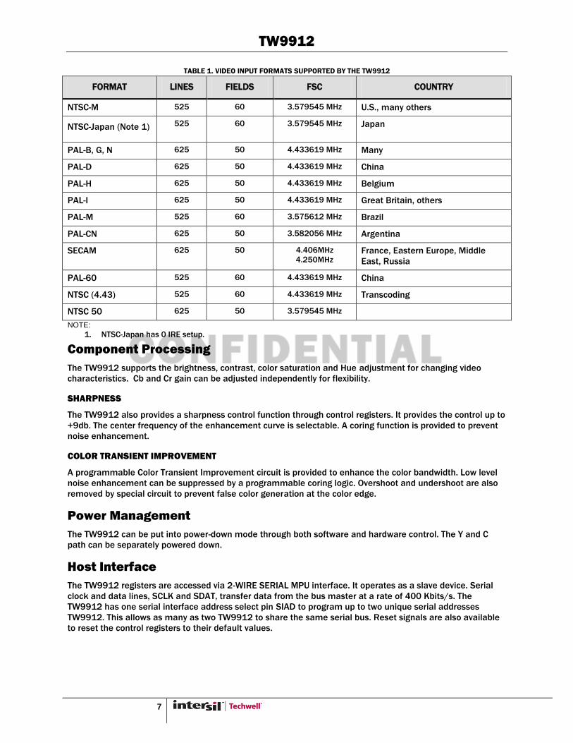
TW9912 supports all common video formats as shown in Table 1. The video decoder needs to be
programmed appropriately for each of the composite video input formats.
TW9912
7
TABLE 1. VIDEO INPUT FORMATS SUPPORTED BY THE TW9912
FORMAT LINES FIELDS FSC COUNTRY
NTSC-M 525 60 3.579545 MHz U.S., many others
NTSC-Japan (Note 1) 525 60 3.579545 MHz Japan
PAL-B, G, N 625 50 4.433619 MHz Many
PAL-D 625 50 4.433619 MHz China
PAL-H 625 50 4.433619 MHz Belgium
PAL-I 625 50 4.433619 MHz Great Britain, others
PAL-M 525 60 3.575612 MHz Brazil
PAL-CN 625 50 3.582056 MHz Argentina
SECAM 625 50 4.406MHz
4.250MHz France, Eastern Europe, Middle
East, Russia
PAL-60 525 60 4.433619 MHz China
NTSC (4.43) 525 60 4.433619 MHz Transcoding
NTSC 50 625 50 3.579545 MHz
NOTE:
1. NTSC-Japan has 0 IRE setup.
Component Processing
The TW9912 supports the brightness, contrast, color saturation and Hue adjustment for changing video
characteristics. Cb and Cr gain can be adjusted independently for flexibility.
SHARPNESS
The TW9912 also provides a sharpness control function through control registers. It provides the control up to
+9db. The center frequency of the enhancement curve is selectable. A coring function is provided to prevent
noise enhancement.
COLOR TRANSIENT IMPROVEMENT
A programmable Color Transient Improvement circuit is provided to enhance the color bandwidth. Low level
noise enhancement can be suppressed by a programmable coring logic. Overshoot and undershoot are also
removed by special circuit to prevent false color generation at the color edge.
Power Management
The TW9912 can be put into power-down mode through both software and hardware control. The Y and C
path can be separately powered down.
Host Interface
The TW9912 registers are accessed via 2-WIRE SERIAL MPU interface. It operates as a slave device. Serial
clock and data lines, SCLK and SDAT, transfer data from the bus master at a rate of 400 Kbits/s. The
TW9912 has one serial interface address select pin SIAD to program up to two unique serial addresses
TW9912. This allows as many as two TW9912 to share the same serial bus. Reset signals are also available
to reset the control registers to their default values.
TW9912
8
Cropping
Cropping allows only subsection of a video image to be output. The VACTIVE signal can be programmed to
indicate the number of active lines to be displayed in a video field, and the HACTIVE signal can be
programmed to indicate the number of active pixels to be displayed in a video line. The start of the field or
frame in the vertical direction is indicated by the leading edge of VSYNC. The start of the line in the horizontal
direction is indicated by the leading edge of the HSYNC. The start of the active lines from the vertical sync
edge is indicated by the VDELAY register. The start of the active pixels from the horizontal edge is indicated
by the HDELAY register. The sizes and locations of the active video are determined by HDELAY, HACTIVE,
VDELAY, and VACTIVE registers. These registers are 8-bit wide, the lower 8-bits are, respectively, in
HDELAY_LO, HACTIVE_LO, VDELAY_LO, and VACTIVE_LO. Their upper 2-bit shares the same register CROP_HI.
In order for the cropping to work properly, the following equation should be satisfied.
HDELAY + HACTIVE < Total number of pixels per line.
VDELAY + VACTIVE < Total number of lines per field
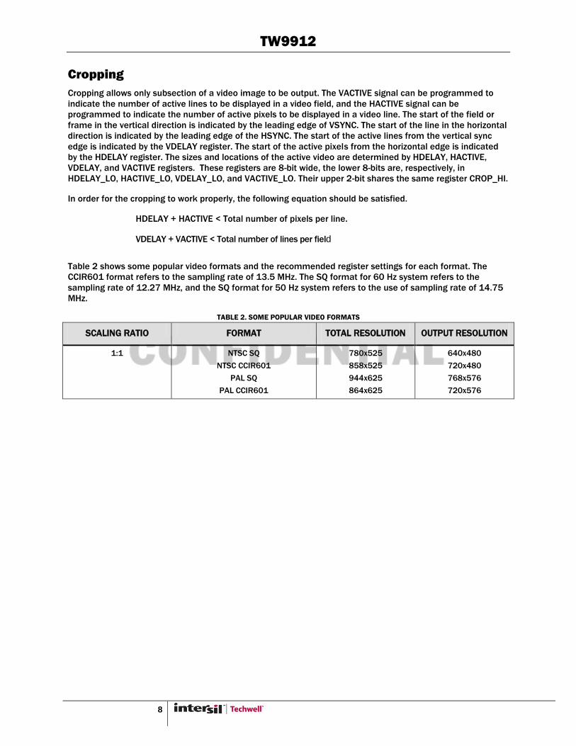
Table 2 shows some popular video formats and the recommended register settings for each format. The
CCIR601 format refers to the sampling rate of 13.5 MHz. The SQ format for 60 Hz system refers to the
sampling rate of 12.27 MHz, and the SQ format for 50 Hz system refers to the use of sampling rate of 14.75
MHz.
TABLE 2. SOME POPULAR VIDEO FORMATS
SCALING RATIO FORMAT TOTAL RESOLUTION OUTPUT RESOLUTION
1:1 NTSC SQ
NTSC CCIR601
PAL SQ
PAL CCIR601
780x525
858x525
944x625
864x625
640x480
720x480
768x576
720x576
TW9912
9
Output Interface
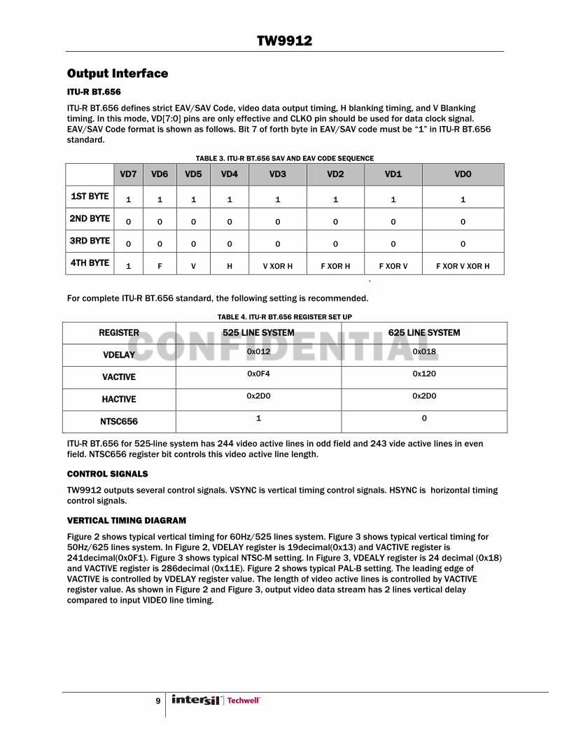
ITU-R BT.656
ITU-R BT.656 defines strict EAV/SAV Code, video data output timing, H blanking timing, and V Blanking
timing. In this mode, VD[7:0] pins are only effective and CLKO pin should be used for data clock signal.
EAV/SAV Code format is shown as follows. Bit 7 of forth byte in EAV/SAV code must be ―1‖ in ITU-R BT.656
standard.
TABLE 3. ITU-R BT.656 SAV AND EAV CODE SEQUENCE
VD7 VD6 VD5 VD4 VD3 VD2 VD1 VD0
1ST BYTE 1 1 1 1 1 1 1 1
2ND BYTE 0 0 0 0 0 0 0 0
3RD BYTE 0 0 0 0 0 0 0 0
4TH BYTE 1 F V H V XOR H F XOR H F XOR V F XOR V XOR H
.
For complete ITU-R BT.656 standard, the following setting is recommended.
TABLE 4. ITU-R BT.656 REGISTER SET UP
REGISTER 525 LINE SYSTEM 625 LINE SYSTEM
VDELAY 0x012 0x018
VACTIVE 0x0F4 0x120
HACTIVE 0x2D0 0x2D0
NTSC656 1 0
ITU-R BT.656 for 525-line system has 244 video active lines in odd field and 243 vide active lines in even
field. NTSC656 register bit controls this video active line length.
CONTROL SIGNALS
TW9912 outputs several control signals. VSYNC is vertical timing control signals. HSYNC is horizontal timing
control signals.
VERTICAL TIMING DIAGRAM
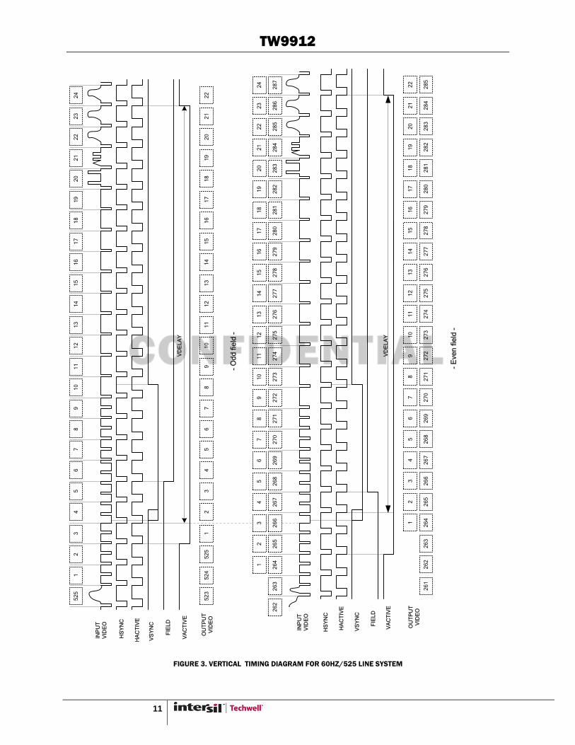
Figure 2 shows typical vertical timing for 60Hz/525 lines system. Figure 3 shows typical vertical timing for
50Hz/625 lines system. In Figure 2, VDELAY register is 19decimal(0x13) and VACTIVE register is
241decimal(0x0F1). Figure 3 shows typical NTSC-M setting. In Figure 3, VDEALY register is 24 decimal (0x18)
and VACTIVE register is 286decimal (0x11E). Figure 2 shows typical PAL-B setting. The leading edge of
VACTIVE is controlled by VDELAY register value. The length of video active lines is controlled by VACTIVE
register value. As shown in Figure 2 and Figure 3, output video data stream has 2 lines vertical delay
compared to input VIDEO line timing.

TW9912
10
INP
UT
VID
EO
HS
YN
C
HA
CT
IVE
VS
YN
C
FIE
LD
VA
CT
IVE
VD
EL
AY
- O
dd
fie
ld -
- E
ve
n f
ield
-
62
26
23
62
46
25
12
34
56
78
91
01
1
62
06
21
62
26
23
62
46
25
12
34
56
78
9..
.1
81
92
02
12
22
32
4
20
21
22
23
24
....
25
26
OU
TP
UT
VID
EO
INP
UT
VID
EO
HS
YN
C
HA
CT
IVE
VS
YN
C
FIE
LD
VA
CT
IVE
VD
EL
AY
31
03
11
31
23
13
31
43
15
31
63
17
31
83
19
32
03
21
32
23
23
32
4..
.3
33
33
43
35
33
63
37
33
83
39
12
34
56
78
91
01
1..
.2
02
12
22
32
42
52
6
30
83
09
31
03
11
31
23
13
31
43
15
31
63
17
31
83
19
32
03
21
32
2..
.3
31
33
23
33
33
43
35
33
63
37
12
34
56
78
9..
.1
81
92
02
12
22
32
4O
UT
PU
T
VID
EO
FIGURE 2. VERTICAL TIMING DIAGRAM FOR 50HZ/625 LINE SYSTEM
TW9912
11
INP
UT
VID
EO
HS
YN
C
HA
CT
IVE
VS
YN
C
FIE
LD
VA
CT
IVE
VD
EL
AY
- O
dd
fie
ld -
INP
UT
VID
EO
12
34
56
78
91
01
11
21
31
41
51
61
71
81
92
02
12
22
32
4
HS
YN
C
HA
CT
IVE
VS
YN
C
FIE
LD
VA
CT
IVE
VD
EL
AY
- E
ve
n f
ield
-
52
51
23
45
67
89
10
11
12
13
14
15
16
17
18
19
20
21
22
23
24
52
35
24
52
51
23
45
67
89
10
11
12
13
14
15
16
17
18
19
20
21
22
OU
TP
UT
VID
EO
26
32
64
26
52
66
26
72
68
26
92
70
27
12
72
27
32
74
27
52
76
27
72
78
27
92
80
28
12
82
28
32
84
28
52
86
28
72
62
12
34
56
78
91
01
11
21
31
41
51
61
71
81
92
02
12
2O
UT
PU
T
VID
EO
26
12
62
26
32
64
26
52
66
26
72
68
26
92
70
27
12
72
27
32
74
27
52
76
27
72
78
27
92
80
28
12
82
28
32
84
28
5
FIGURE 3. VERTICAL TIMING DIAGRAM FOR 60HZ/525 LINE SYSTEM

TW9912
12
HSYNC
The leading edge of HSYNC signal is synchronized to input Video horizontal sync timing.
VSYNC
The leading edge of VSYNC signal is synchronized to vertical sync pulse of input Video.
FIELD
The FIELD signal can be output on the MPOUT pin if the RTSEL register selects the FIELD output. Figure 2 and
Figure 3 show field signal output as default.
Closed Captioning and Extended Data Services
Line 21 Closed Captioning and line 284 Extended Data Service of 525-line video system is at a 0.5035MHz
bit rate. Line 22, line 335 Closed Captioning of 625-line video system is at about 0.500MHz.It contains 14bits
Clock Run-in by double bit rate, 3bits Start Bits, and 2 bytes data. Each of these 2 bytes is a 7 bit + odd parity
ASCII character which represents text or control characters for positioning or display control. For the purposes
of CC or EDS, only the Y component of the video signal is used. The TW9912 can be programmed to decode
CC or EDS data by setting register 0x1A. Since the CC and EDS are independent, there could be one or both in
a particular frame. A typical waveform is shown in Figure 4.
CC/EDS decoder uses the internal low pass filtered VBI data with ADC sampling rate. CC/EDS Bit rate
frequency is generated internally.
In the CC/EDS decode mode, the decoder monitors the appropriate scan lines looking for the clock run-in and
start bits pattern. If it‘s found, it starts tracking Clock Run-in Frequency and checks the status of Clock Run-in
and start bits. Some programming may use these scan lines for other purpose. The caption data is sampled
and loaded into shift registers, and the data is then transferred to the caption data FIFO. The TW9912
provides a 16 x 10 location FIFO for storing CC/EDS data. Once the video decoder detects the correct status
of Clock Run-in, Start Bits in the CC/EDS signal, it captures the low byte of CC/EDS data at first and high byte
next. Data is stored in the FIFO low byte first and high byte next sequentially. Captioned data is available to
the user through the CC_DATA register (0x1B). Upon being placed in the 10-bit FIFO, two additional bits are
attached to the CC/EDS data byte by TW9912‘s CC/EDS decoder. These two bits indicate whether the given
byte stored in the FIFO corresponds to CC or EDS data and whether it is the high or low byte of CC/EDS. These
two bits are available to the user through the CC_STATUS register bits CC_EDS and LO_HI(0x1A[1:0]),
respectively. As stored in the FIFO, LO_HI is bit 8 and CC_EDS is bit 9. Additionally, the TW9912 reports the
Clock run-in Frame code
2-byte character data
FIGURE 4. TYPICAL CC/EDS SCAN LINE WAVEFORM

TW9912
13
results of the parity check in the PARITY bit in the CC_STATUS register. FIFO can hold 17 data. Initially when
the FIFO is empty, bit FF_EMP in the CC_STATUS register (0x1A[2]) is set low indicating that no data is
available in the FIFO. Subsequently, when data has been stored in the FIFO, the FF_EMP bit is set to logical
high. If the FIFO read cycle time is long, then FIFO overflow condition may happen. After 17 data are stored in
FIFO, FF_OVF bit in CC_STATUS register(0x1A[3]) becomes high. After FF_OVF becomes high, any incoming
data causes only 17th location data to be overwritten. After FIFO is read and FIFO has less than 16 data,
FF_OVF bit becomes low. However, once FF_OVF bit becomes high some data loss may happen. In this case,
FIFO must be reset by the following way (a) or (b). Method (b) is most often used.
(a) Execute Software Reset (Write 0x06[7]=1)
(b) Write CC_STATUS register bits 0x1A[6:5]=00
16 times read CC_DATA register 0x1B continuously
Write CC_STATUS Register bits 0x1A[6:5] for the application again
There will routinely be asynchronous reads and writes to the CC/EDS FIFO. The writes will be from the
CC/EDS circuitry and the reads will occur as the system controller reads the CC/EDS data from TW9912.
These reads and writes will not occur until FIFO is in overflow condition. The average FIFO Read cycle time
must be shorter than Closed Captioning byte transmitter cycle time. If either odd field Close Captioning or
even field Closed Captioning is enabled, the average FIFO read cycle time must be shorter than 2 times write
per 1 frame cycle. If both odd field Closed Captioning and even field Closed Captioning are enabled, it must
be shorter than 4 times write per 1 frame cycle. Otherwise, FIFO will be in overflow condition theoretically.
Typical FIFO Read flows are as follows. This flow is written similar to C language type.
Case : typical Two-wire Serial Bus Master with normal read cycle speed
CONT1: Write CC_STATUS register bits 0x1A[6:5]=00
Read 16 times CC_DATA register 0x1B
Write CC_STATUS register bits 0x1A[6:5] for the application
CONT2: Read CC_STATUS register 0x1A
If(FF_OVF bit==1) goto CONT1
else if(FF_EMP bit ==0) goto CONT2 or goto CONT3
else {
if(PARITY bit==1) {
read CC_DATA register 0x1B
Abandon this CC_DATA
goto CONT2 or goto CONT3
}
else {
Check CC_EDS bit and store field information
read CC_DATA register 0x1B(store 1 data)
}
}
CONT3: execute another program routine
goto CONT2

TW9912
14
Two Wire Serial Bus Interface
SDAT
Start Condition Stop Condition
SCLK
SCLK
Device ID (1-7) R/W Index (1-8) Data (1-8)
SDAT
Start Condition
Stop Condition
Ack Ack Ack
Re-start Condition
SCLK
Device ID (1-7) R/W Index (1-8)
SDAT
Ack Ack
Data (1-8)
Stop Condition Nack
Start Condition
Device ID (1-7) R/W
Ack
FIGURE 5. DEFINITION OF THE SERIAL BUS INTERFACE BUS START AND STOP
FIGURE 6. ONE COMPLETE REGISTER READ SEQUENCE VIA THE SERIAL BUS INTERFACE
FIGURE 7. ONE COMPLETE REGISTER WRITE SEQUENCE VIA THE SERIAL BUS INTERFACE
TW9912
15
The two wire serial bus interface is used to allow an external micro-controller to write control data to, and
read control or other information from the TW9912 registers. SCLK is the serial clock and SDAT is the data
line. Both lines are pulled high by resistors connected to VDD33. ICs communicate on the bus by pulling SCLK
and SDAT low through open drain outputs. In normal operation, the master generates all clock pulses, but
control of the SDAT line alternates back and forth between the master and the slave. For both read and write,
each byte is transferred MSB first, and the data bit is valid whenever SCLK is high.
The TW9912 is operated as a bus slave device. It can be programmed to respond to one of two 7-bit slave
device addresses by tying the SIAD (Serial Interface Address) pin to either VDD33 or VSS33 (see Table 5)
through a pull-up or pull-down resister. If the SIAD pin is tied to VDD33, then the least significant bit of the 7-
bit address is a ―1‖. If the SIAD pin is tied to VSS33 then the least significant bit of the 7-bit address is a ―0‖.
The most significant 6-bits are fixed. The 7-bit address field is concatenated with the read/write control bit to
form the first byte transferred during a new transfer. If the read/write control bit is high,the next byte will be
read from the slave device. If it is low,the next byte will be write to the slave. When a bus master (the host
microprocessor) drives SDAT from high to low, while SCLK is high, this is defined to be a start condition (See
Figure 5). All slaves on the bus listen to determine when a start condition has been asserted.
After a start condition, all slave devices listen for the their device addresses. The host then sends a byte
consisting of the 7-bit slave device ID and the R/W bit. This is shown in Figure 6. (For the TW9912, the next
byte is normally the index to the TW9912 registers and is a write to the TW9912 therefore the first R/W bit is
normally low.)
After transmitting the device address and the R/W bit, the master must release the SDAT line while holding
SCLK low, and wait for an acknowledgement from the slave. If the address matches the device address of a
slave, the slave will respond by driving the SDAT line low to acknowledge the condition. The master will then
continue with the next 8-bit transfer. If no device on the bus responds, the master transmits a stop condition
and ends the cycle. Notice that a successful transfer always includes nine clock pulses.
To write to the internal register of theTW9912, the master sends another 8-bits of data, the TW9912 loads
this to the register pointed by the internal index register. The TW9912 will acknowledge the 8-bit data
transfer and automatically increment the index in preparation for the next data. The master can do multiple
writes to the TW9912 if they are in ascending sequential order. After each 8-bit transfer the TW9912 will
acknowledge the receipt of the 8-bits with an acknowledge pulse. To end all transfers to the TW9912 the
host will issue a stop condition.
TABLE 5. TW9912 SERIAL BUS INTERFACE 7-BIT SLAVE ADDRESS AND READ WRITE BIT
SERIAL BUS INTERFACE 7-BIT SLAVE ADDRESS READ/WRITE
BIT
1 0 0 0 1 0 SIAD 1=Read
0=Write
A TW9912 read cycle has two phases. The first phase is a write to the internal index register. The second
phase is the read from the data register. See Figure 6. The host initiates the first phase by sending the start
condition. It then sends the slave device ID together with a 0 in the R/W bit position. The index is then sent
followed by either a stop condition or a second start condition. The second phase starts with the second start
condition. The master then resends the same slave device ID with a 1 in the R/W bit position to indicate a
read. The slave will transfer the contents of the desired register. The master remains in control of the clock.
After transferring eight bits, the slave releases, the master takes control of the SDAT line and acknowledges
the receipt of data to the slave. To terminate the last transfer the master will issue a negative acknowledge
(SDAT is left high during a clock pulse) and issue a stop condition.

TW9912
16
Filter Curves
ANTI-ALIAS FILTER
DECIMATION FILTER
0 2 4 6 8 10 12
x 106
-50
-45
-40
-35
-30
-25
-20
-15
-10
-5
0
Frequency (Hertz)
Mag
nitu
de R
espo
nse
(dB
)
0 0.2 0.4 0.6 0.8 1 1.2 1.4 1.6 1.8 2
x 107
-40
-35
-30
-25
-20
-15
-10
-5
0
Frequency (Hertz)
Gai
n (d
B)
TW9912
17
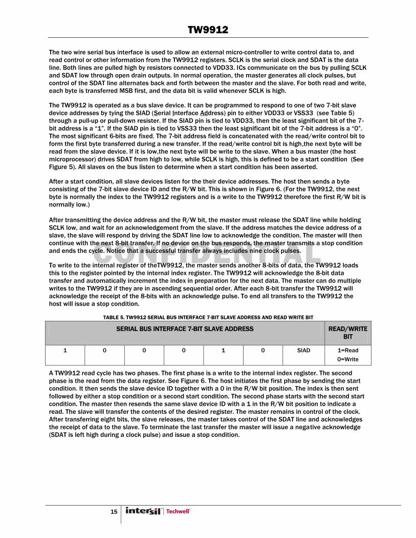
CHROMA BAND PASS FILTER CURVES
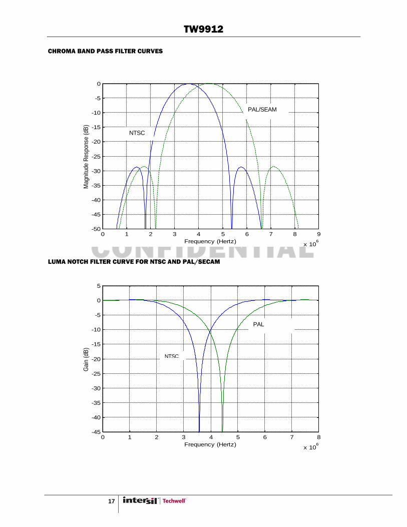
LUMA NOTCH FILTER CURVE FOR NTSC AND PAL/SECAM
0 1 2 3 4 5 6 7 8
x 106
-45
-40
-35
-30
-25
-20
-15
-10
-5
0
5
Frequency (Hertz)
Gai
n (d
B)
0 1 2 3 4 5 6 7 8 9
x 106
-50
-45
-40
-35
-30
-25
-20
-15
-10
-5
0
Frequency (Hertz)
Mag
nitu
de R
espo
nse
(dB
)
PAL/SEAM
NTSC
PAL
NTSC
TW9912
18
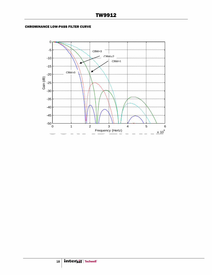
CHROMINANCE LOW-PASS FILTER CURVE
Low Med
High
Low
Med
High
0 1 2 3 4 5 6
x 106
-50
-45
-40
-35
-30
-25
-20
-15
-10
-5
0
Frequency (Hertz)
Gain
(dB
)
CBW=0
CBW=3
CBW=1
CBW=2
TW9912
19
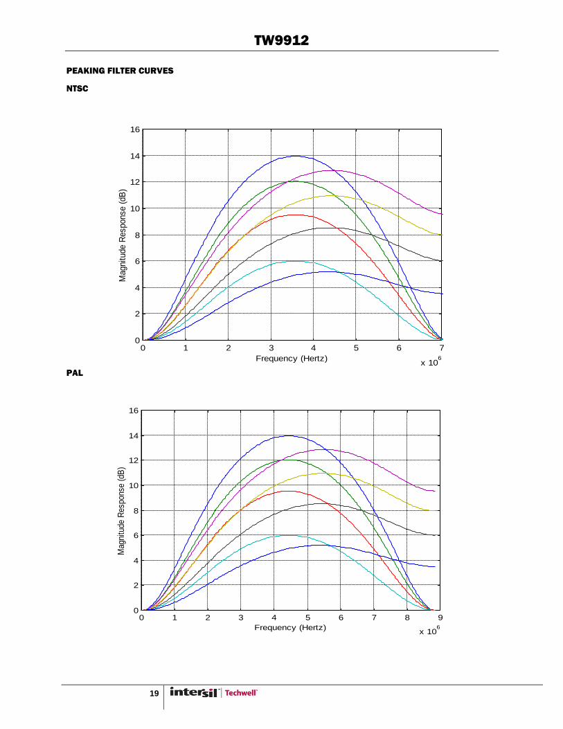
PEAKING FILTER CURVES
NTSC
PAL
0 1 2 3 4 5 6 7
x 106
0
2
4
6
8
10
12
14
16
Frequency (Hertz)
Magnitude R
esponse (
dB
)
0 1 2 3 4 5 6 7 8 9
x 106
0
2
4
6
8
10
12
14
16
Frequency (Hertz)
Mag
nitu
de R
espo
nse
(dB
)

TW9912
20
Pin Configuration
48 Pin QFN
AV
SP
L
AV
DP
L
NC
VS
IN
HS
IN
TE
ST
VD
D
VS
S
VS
O
HS
O
MP
OU
T
VS
S33
VDD33
CLKO
VD7
VD6
VD5
VD4
NC
VD3
VD2
VD1
VD0
VDD33
SOG
AVSAD
CIN1
CIN0
YOUT/YIN3
YIN2
YIN1
YIN0
VIN1
VIN0
AVDAD
NC
TM
OD
E
SIA
D
PD
N
SD
AT
SC
LK
NC
VD
D
VS
S
XT
I
XT
O
RS
TB
VS
S33
TW9912
48
47
46
45
44
43
42
41
40
39
38
37
36
35
34
1
2
3
4
5
6
7
8
9
10
11
12
36
35
34
33
32
31
30
29
28
27
26
25
13
14
15
16
17
18
19
20
21
22
23
24
TW9912
21
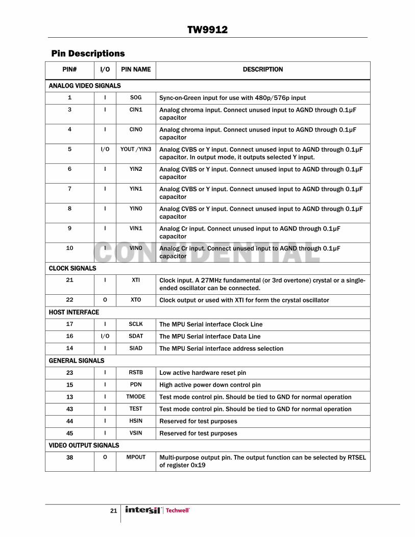
Pin Descriptions
PIN# I/O PIN NAME DESCRIPTION
ANALOG VIDEO SIGNALS
1 I SOG Sync-on-Green input for use with 480p/576p input
3 I CIN1 Analog chroma input. Connect unused input to AGND through 0.1µF
capacitor
4 I CIN0 Analog chroma input. Connect unused input to AGND through 0.1µF
capacitor
5 I/O YOUT /YIN3 Analog CVBS or Y input. Connect unused input to AGND through 0.1µF
capacitor. In output mode, it outputs selected Y input.
6 I YIN2 Analog CVBS or Y input. Connect unused input to AGND through 0.1µF
capacitor
7 I YIN1 Analog CVBS or Y input. Connect unused input to AGND through 0.1µF
capacitor
8 I YIN0 Analog CVBS or Y input. Connect unused input to AGND through 0.1µF
capacitor
9 I VIN1 Analog Cr input. Connect unused input to AGND through 0.1µF
capacitor
10 I VIN0 Analog Cr input. Connect unused input to AGND through 0.1µF
capacitor
CLOCK SIGNALS
21 I XTI Clock input. A 27MHz fundamental (or 3rd overtone) crystal or a single-
ended oscillator can be connected.
22 O XTO Clock output or used with XTI for form the crystal oscillator
HOST INTERFACE
17 I SCLK The MPU Serial interface Clock Line
16 I/O SDAT The MPU Serial interface Data Line
14 I SIAD The MPU Serial interface address selection
GENERAL SIGNALS
23 I RSTB Low active hardware reset pin
15 I PDN High active power down control pin
13 I TMODE Test mode control pin. Should be tied to GND for normal operation
43 I TEST Test mode control pin. Should be tied to GND for normal operation
44 I HSIN Reserved for test purposes
45 I VSIN Reserved for test purposes
VIDEO OUTPUT SIGNALS
38 O MPOUT Multi-purpose output pin. The output function can be selected by RTSEL
of register 0x19

TW9912
22
PIN# I/O PIN NAME DESCRIPTION
39 O HSO Horizontal sync and multi-purpose output pin. See register for control
information.
40 O VSO Vertical Sync and multi-purpose output. See register for control
information.
35 O CLKO Data Clock output. See register for control information.
34
33
32
31
29
28
27
26
I/O VD[7-0] Digitized video data output of 4:2:2 YCbCr. VD[7] is the MSB
12, 18, 30, 46 NC No connection
POWER AND GROUND PINS
PIN# I/O PIN NAME DESCRIPTION
19,42 I VDD 1.8V digital core power
20,41 I VSS 1.8V digital core return
25, 36 I VDD33 3.3V digital I/O power
24, 37 I VSS33 3.3V digital I/O return
11 I AVDAD 1.8V analog ADC supply
2 I AVSAD 1.8V analog ADC return
47 I AVDPL 1.8V PLL supply
48 I AVSPL 1.8V PLL return
TW9912
23
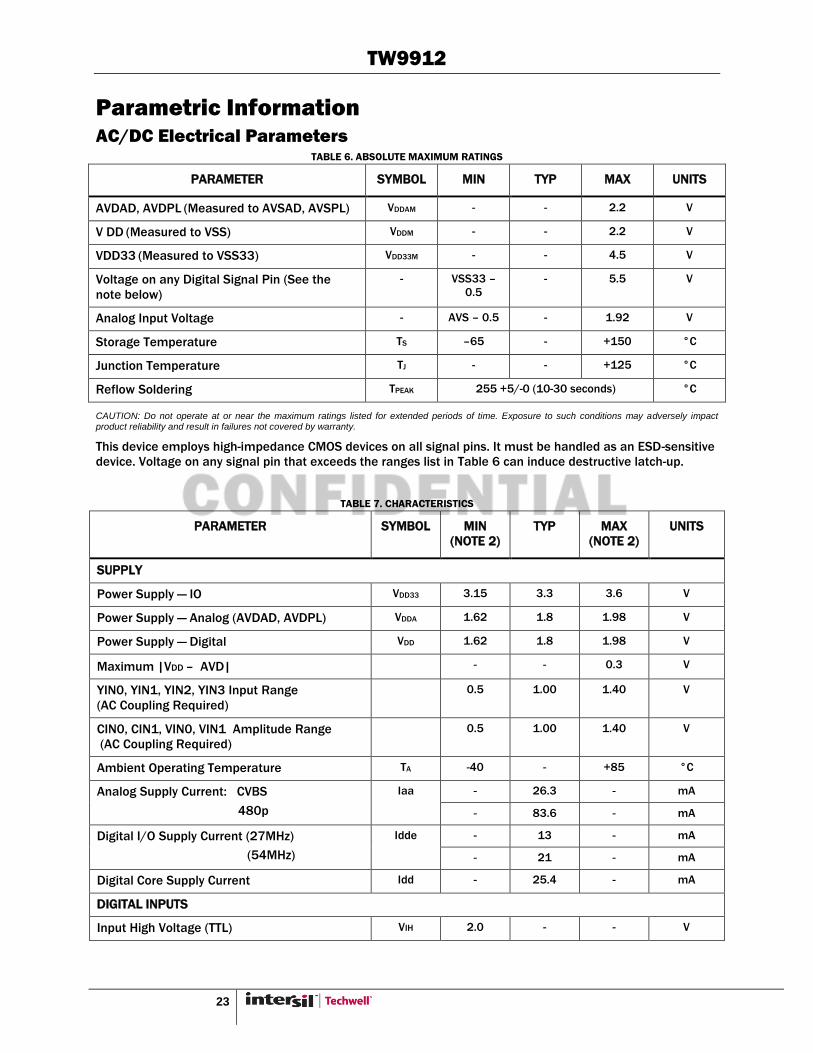
Parametric Information
AC/DC Electrical Parameters TABLE 6. ABSOLUTE MAXIMUM RATINGS
PARAMETER SYMBOL MIN TYP MAX UNITS
AVDAD, AVDPL (Measured to AVSAD, AVSPL) VDDAM - - 2.2 V
V DD (Measured to VSS) VDDM - - 2.2 V
VDD33 (Measured to VSS33) VDD33M - - 4.5 V
Voltage on any Digital Signal Pin (See the
note below)
- VSS33 –
0.5 - 5.5 V
Analog Input Voltage - AVS – 0.5 - 1.92 V
Storage Temperature TS –65 - +150 °C
Junction Temperature TJ - - +125 °C
Reflow Soldering TPEAK 255 +5/-0 (10-30 seconds) °C
CAUTION: Do not operate at or near the maximum ratings listed for extended periods of time. Exposure to such conditions may adversely impact product reliability and result in failures not covered by warranty.
This device employs high-impedance CMOS devices on all signal pins. It must be handled as an ESD-sensitive
device. Voltage on any signal pin that exceeds the ranges list in Table 6 can induce destructive latch-up.
TABLE 7. CHARACTERISTICS
PARAMETER SYMBOL MIN
(NOTE 2)
TYP MAX
(NOTE 2)
UNITS
SUPPLY
Power Supply — IO VDD33 3.15 3.3 3.6 V
Power Supply — Analog (AVDAD, AVDPL) VDDA 1.62 1.8 1.98 V
Power Supply — Digital VDD 1.62 1.8 1.98 V
Maximum |VDD – AVD| - - 0.3 V
YIN0, YIN1, YIN2, YIN3 Input Range
(AC Coupling Required)
0.5 1.00 1.40 V
CIN0, CIN1, VIN0, VIN1 Amplitude Range
(AC Coupling Required)
0.5 1.00 1.40 V
Ambient Operating Temperature TA -40 - +85 °C
Analog Supply Current: CVBS
480p
Iaa - 26.3 - mA
- 83.6 - mA
Digital I/O Supply Current (27MHz)
(54MHz)
Idde - 13 - mA
- 21 - mA
Digital Core Supply Current Idd - 25.4 - mA
DIGITAL INPUTS
Input High Voltage (TTL) VIH 2.0 - - V

TW9912
24
PARAMETER SYMBOL MIN
(NOTE 2)
TYP MAX
(NOTE 2)
UNITS
Input Low Voltage (TTL) VIL - - 0.8 V
Input High Voltage (XTI) VIH 2.0 - V DD33 +
0.5
V
Input Low Voltage (XTI) VIL - - 0.8 V
Input High Current (VIN = V DD ) IIH - - 10 A
Input Low Current (VIN = VSS) IIL - - –10 A
Input Capacitance (f =1 MHz, VIN = 2.4 V) CIN - 5 - pF
PARAMETER SYMBOL MIN
(NOTE 2)
TYP MAX
(NOTE 2)
UNITS
DIGITAL OUTPUTS
Output High Voltage (IOH = –2 mA) VOH 2.4 - VDD33 V
Output Low Voltage (IOL = 2 mA) VOL - 0.2 0.4 V
3-State Current IOZ - - 10 A
Output Capacitance CO - 5 - pF
ANALOG INPUT
Analog Pin Input Voltage Vi - 1 - Vpp
Analog Pin Input Capacitance CA - 7 - pF
ADCS
ADC Resolution ADCR - 10 - bits
ADC Integral Non-linearity AINL - 1 - LSB
ADC Differential Non-Linearity ADNL - 1 - LSB
ADC Clock Rate fADC 24 54 60 MHz
Video Bandwidth (-3db) BW - 10 - MHz
HORIZONTAL PLL (DECODER)
Line Frequency (50Hz) fLN - 15.625 - KHz
Line Frequency (60Hz) fLN - 15.734 - KHz
Static Deviation fH - - 6.2 %
SUBCARRIER PLL (DECODER)
Subcarrier Frequency (NTSC-M) fSC - 3579545 - Hz
Subcarrier Frequency (PAL-BDGHI) fSC - 4433619 - Hz
Subcarrier Frequency (PAL-M) fSC - 3575612 - Hz
Subcarrier Frequency (PAL-N) fSC - 3582056 - Hz
Lock In Range fH 450 - - Hz

TW9912
25
PARAMETER SYMBOL MIN
(NOTE 2)
TYP MAX
(NOTE 2)
UNITS
CRYSTAL SPEC
Nominal Frequency (Fundamental) - 27 - MHz
Deviation (Note 1) - - 50 ppm
Load Capacitance CL - 20 - pF
Series Resistor RS - 80 - Ω
OSCILLATOR INPUT
Nominal Frequency - 27 - MHz
Deviation - - 50 ppm
Duty Cycle - - 55 %
NOTE:
1. Crystal deviation is based on normal operation condition.
2. Compliance to datasheet limits is assured by one or more methods: production test, characterization and/or
design.

TW9912
26
OUTPUT TIMING
NOTE:
1. Compliance to datasheet limits is assured by one or more methods: production test, characterization and/or
design.
PARAMETER SYMBOL MIN
(NOTE 1)
TYP MAX
(NOTE 1)
UNITS
Output Clock Duty 40% 50% 60%
CLKO High Period 27MHz t1 - 18.5 - ns
54MHz 9.26
CLKO Low Period 27MHz t2 - 18.5 - ns
54MHz 9.26
Data Output Hold
CK2S = 0 & VDSEL = 0 & CK2P = 1
CK2S = 1 & VDSEL = 1 & CK2P = 1
CK2S = 2 & VDSEL = 2 & CK2P = 1
t3 -
2
-
ns
2
2
Data Output Delay
CK2S = 0 & VDSEL = 0 & CK2P = 1
CK2S = 1 & VDSEL = 1 & CK2P = 1
CK2S = 2 & VDSEL = 2 & CK2P = 1
t4 -
6
-
ns
6
6
CLKO
VD
t1
t2
t3
t4
TW9912
27
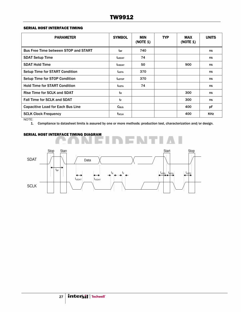
SERIAL HOST INTERFACE TIMING
PARAMETER SYMBOL MIN
(NOTE 1)
TYP MAX
(NOTE 1)
UNITS
Bus Free Time between STOP and START tBF 740 ns
SDAT Setup Time tsSDAT 74 ns
SDAT Hold Time thSDAT 50 900 ns
Setup Time for START Condition tsSTA 370 ns
Setup Time for STOP Condition tsSTOP 370 ns
Hold Time for START Condition thSTA 74 ns
Rise Time for SCLK and SDAT tR 300 ns
Fall Time for SCLK and SDAT tF 300 ns
Capacitive Load for Each Bus Line CBUS 400 pF
SCLK Clock Frequency fSCLK 400 KHz
NOTE:
1. Compliance to datasheet limits is assured by one or more methods: production test, characterization and/or design.
SERIAL HOST INTERFACE TIMING DIAGRAM
Stop Start
Data
StopStart
SDAT
SCLK
tBFthSTA tsSTOtsSTA
tsSDAT
tR tF
thSDAT

TW9912
28
Package Outline Drawing

TW9912
29
Application Schematics
YIN0
YIN1
CIN0
22pf27M1 Mohm
22pf
L1 , 3.3uHC1 , 220pf
XTI
XTO
RSTB
VD0- 7
Video
Timing
SCL
SDA
PDN
AGND
DGND
0.1uF
AVDAD
AVDPL
AVSAD
AVSPL
0.1uF
VDD
VDD33
VSS
VSS33
GND
1.8V
3.3V
Filtered 1.8V
Typical TW9912 External Circuitry
4.7k
4.7k
3.3/5V
TW9912
CVBS1
S- Video
Note: All unused digital input pins should be tied to DGND.
*
* For 3 rd overtone crystal
0.1uF75 ohm
0.1uF75 ohm
0.1uF75 ohm
SIAD
3.3V
** option10k

TW9912
30
PCB LAYOUT CONSIDERATIONS
The PCB layout should be done to minimize the power and ground noise on the TW9912. This is done by good power
de-coupling with minimum lead length on the de-coupling capacitors; well-filtered and regulated analog power input
shielding and ground plane isolation.
The ground plane should cover most of the PCB area with separated digital and analog ground planes surrounding
the chip. These two planes should be at the same electrical potential and connected together under TW9912. The
following figure shows a ground plane layout example.
AGND
DGND
TW9912
To minimize crosstalk, the digital signals of TW9912 should be separated from the analog circuitry. Moreover, the
digital signals should not cross over the analog power and ground plane. Parallel running of digital lines for long
distance should also be avoided.
For QFN Package, the Exposed die pad (Ground bond) can be either floating or soldered to PCB Ground to enhance
thermal performance.
Exposed Die Pad
QFN
TW9912
31
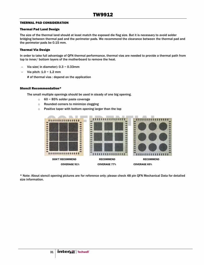
THERMAL PAD CONSIDERATION
Thermal Pad Land Design
The size of the thermal land should at least match the exposed die flag size. But it is necessary to avoid solder
bridging between thermal pad and the perimeter pads. We recommend the clearance between the thermal pad and
the perimeter pads be 0.15 mm.
Thermal Via Design
In order to take full advantage of QFN thermal performance, thermal vias are needed to provide a thermal path from
top to inner/ bottom layers of the motherboard to remove the heat.
Via size( in diameter): 0.3 ~ 0.33mm
Via pitch: 1.0 ~ 1.2 mm
# of thermal vias : depend on the application
Stencil Recommendation*
The small multiple openings should be used in steady of one big opening.
o 60 ~ 85% solder paste coverage
o Rounded corners to minimize clogging
o Positive taper with bottom opening larger than the top
DON’T RECOMMEND RECOMMEND RECOMMEND
COVERAGE 91% COVERAGE 77% COVERAGE 65%
* Note: About stencil opening pictures are for reference only; please check 48 pin QFN Mechanical Data for detailed
size information.

TW9912
32
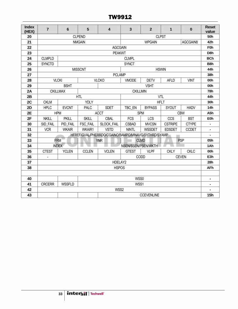
TW9912 Register Summary The registers are organized in functional groups in this Register Summary.
―-―: for Register it means ―Reserved‖, for Reset Value it means ―unknown‖
Index (HEX)
7 6 5 4 3 2 1 0 Reset value
00 ID REV 60h
01 VDLOSS HLOCK SLOCK FIELD VLOCK - MONO DET50 -
02 - FC27 CVIDEO SVIDEO YSEL CSEL0 VSEL 40h
03 - - LLCMD AINC - OEN TRI_SEL 24h
04 - CKHY HSDLY 00h
05 VDSEL HSP VSP HVSEL 00h
06 SRESET IREF VREF AGC_EN CLKPDN Y_PDN C_PDN V_PDN 00h
07 VDELAY_HI VACTIVE_HI HDELAY_HI HACTIVE_HI 12h
08 VDELAY_LO 12h
09 VACTIVE_LO F0h
0A HDELAY_LO 10h
0B HACTIVE_LO D0h
0C PBW DEM PALSW SET7 COMB HCOMP YCOMB PDLY CCh
0D - NTSC656 WSSEN CCODDLINE 15h
0E -
0F - 00h
10 BRIGHTNESS 00h
11 CONTRAST 64h
12 SCURVE VSF CTI SHARPNESS 11h
13 SAT_U 80h
14 SAT_V 80h
15 HUE 00h
16 - -
17 SHCOR - VSHP 30h
18 CTCOR CCOR VCOR CIF 44h
19 - RTSEL 58h
1A - EDS_EN CC_EN PARITY FF_OVF FF_EMP CC_EDS LO_HI 00h
1B CC_DATA -
1C DTSTUS STDNOW ATREG STANDARD 07h
1D START PAL60 PALCN PALM NTSC4 SECAM PALB NTSCM 7Fh
1E NT50 CVSTD CVFMT 08h
1F TEST 00h
TW9912
33
Index (HEX)
7 6 5 4 3 2 1 0 Reset value
20 CLPEND CLPST 50h
21 NMGAIN WPGAIN AGCGAIN8 42h
22 AGCGAIN F0h
23 PEAKWT D8h
24 CLMPLD CLMPL BCh
25 SYNCTD SYNCT B8h
26 MISSCNT HSWIN 44h
27 PCLAMP 38h
28 VLCKI VLCKO VMODE DETV AFLD VINT 00h
29 BSHT VSHT 00h
2A CKILLMAX CKILLMIN 78h
2B HTL VTL 44h
2C CKLM YDLY HFLT 30h
2D HPLC EVCNT PALC SDET TBC_EN BYPASS SYOUT HADV 14h
2E HPM ACCT SPM CBW A5h
2F NKILL PKILL SKILL CBAL FCS LCS CCS BST E0h
30 SID_FAIL PID_FAIL FSC_FAIL SLOCK_FAIL CSBAD MVCSN CSTRIPE CTYPE -
31 VCR WKAIR WKAIR1 VSTD NINTL WSSDET EDSDET CCDET -
32 HFREF/GVAL/PHERRDO/CGAINO/BAMPO/MINAVG/SYTHRD/SYAMP -
33 FRM YNR CLMD PSP 05h
34 INDEX NSEN/SSEN/PSEN/WKTH 1Ah
35 CTEST YCLEN CCLEN VCLEN GTEST VLPF CKLY CKLC 00h
36 - CODD CEVEN E3h
37 HDELAY2 28h
38 HSPOS AFh
40 WSS0 -
41 CRCERR WSSFLD WSS1 -
42 WSS2 -
43 CCEVENLINE 15h
TW9912
34
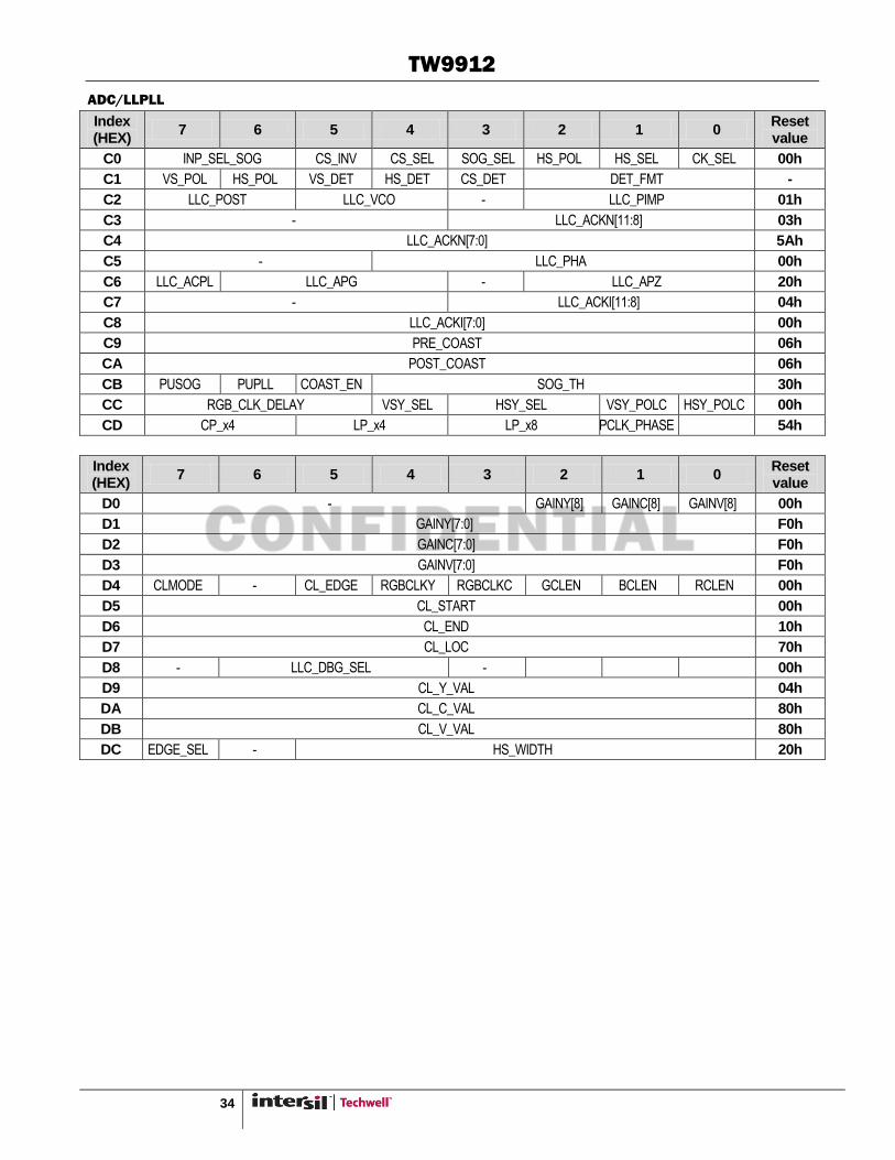
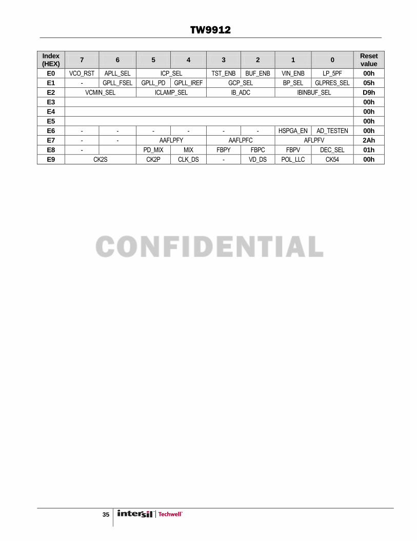
ADC/LLPLL
Index (HEX)
7 6 5 4 3 2 1 0 Reset value
C0 INP_SEL_SOG CS_INV CS_SEL SOG_SEL HS_POL HS_SEL CK_SEL 00h
C1 VS_POL HS_POL VS_DET HS_DET CS_DET DET_FMT -
C2 LLC_POST LLC_VCO - LLC_PIMP 01h
C3 - LLC_ACKN[11:8] 03h
C4 LLC_ACKN[7:0] 5Ah
C5 - LLC_PHA 00h
C6 LLC_ACPL LLC_APG - LLC_APZ 20h
C7 - LLC_ACKI[11:8] 04h
C8 LLC_ACKI[7:0] 00h
C9 PRE_COAST 06h
CA POST_COAST 06h
CB PUSOG PUPLL COAST_EN SOG_TH 30h
CC RGB_CLK_DELAY VSY_SEL HSY_SEL VSY_POLC HSY_POLC 00h
CD CP_x4 LP_x4 LP_x8 PCLK_PHASE 54h
Index (HEX)
7 6 5 4 3 2 1 0 Reset value
D0 - GAINY[8] GAINC[8] GAINV[8] 00h
D1 GAINY[7:0] F0h
D2 GAINC[7:0] F0h
D3 GAINV[7:0] F0h
D4 CLMODE - CL_EDGE RGBCLKY RGBCLKC GCLEN BCLEN RCLEN 00h
D5 CL_START 00h
D6 CL_END 10h
D7 CL_LOC 70h
D8 - LLC_DBG_SEL - 00h
D9 CL_Y_VAL 04h
DA CL_C_VAL 80h
DB CL_V_VAL 80h
DC EDGE_SEL - HS_WIDTH 20h
TW9912
35
Index (HEX)
7 6 5 4 3 2 1 0 Reset value
E0 VCO_RST APLL_SEL ICP_SEL TST_ENB BUF_ENB VIN_ENB LP_5PF 00h
E1 - GPLL_FSEL GPLL_PD GPLL_IREF GCP_SEL BP_SEL GLPRES_SEL 05h
E2 VCMIN_SEL ICLAMP_SEL IB_ADC IBINBUF_SEL D9h
E3 00h
E4 00h
E5 00h
E6 - - - - - - HSPGA_EN AD_TESTEN 00h
E7 - - AAFLPFY AAFLPFC AFLPFV 2Ah
E8 - PD_MIX MIX FBPY FBPC FBPV DEC_SEL 01h
E9 CK2S CK2P CLK_DS - VD_DS POL_LLC CK54 00h

TW9912
36
0X01 – CHIP STATUS REGISTER (CSTATUS)
BIT FUNCTION R/W DESCRIPTION RESET
7 VDLOSS R 1 = Video not present. (sync is not detected in number of consecutive line
periods specified by MISSCNT register)
0 = Video detected
-
6 HLOCK R 1 = Horizontal sync PLL is locked to the incoming video source
0 = Horizontal sync PLL is not locked
-
5 SLOCK R 1 = Sub-carrier PLL is locked to the incoming video source
0 = Sub-carrier PLL is not locked
-
4 FIELD R 0 = Odd field is being decoded
1 = Even field is being decoded
-
3 VLOCK R 1 = Vertical logic is locked to the incoming video source
0 = Vertical logic is not locked
-
2 Reserved R Reserved -
1 MONO R 1 = No color burst signal detected
0 = Color burst signal detected
-
0 DET50 R 0 = 60Hz source detected
1 = 50Hz source detected
The actual vertical scanning frequency depends on the current standard invoked
-
0X02 – INPUT FORMAT (INFORM)
BIT FUNCTION R/W DESCRIPTION RESET
7 CSEL1 R/W Reserved 0
6 FC27 R/W 1 = Input crystal clock frequency is 27MHz
0 = Square pixel mode. Must use 24.54MHz for 60Hz field rate source or
29.5MHz for 50Hz field rate source.
1
5-4 IFSEL R/W 0 = Composite video decoding
1 = S-video decoding
2 = Component video decoding (Interlace input)
3 = Component video decoding (Progressive input)
0
3-2 YSEL R/W These two bits control the input video selection. It selects the composite video
source or Luma source.
0 = YIN0 1 = YIN1 2 = YIN2 3 = YIN3
0

TW9912
37
BIT FUNCTION R/W DESCRIPTION RESET
1 CSEL0 R/W These bit select the C channel input
0 = CIN0 1 = CIN1
0
0 VSEL R/W This bit select the V channel input
0 = VIN0 1 = VIN1
0
0X03 – OUTPUT CONTROL REGISTER (OPFORM)
BIT FUNCTION R/W DESCRIPTION RESET
7 R/W Reserved 0
6 R/W Reserved 0
5 LLCMODE R/W 1 = LLC output mode. 0 = Reserved 1
4 AINC R/W Serial interface auto-indexing control
0 = auto-increment 1 = non-auto
0
3 R/W Reserved 0
2 OEN R/W Output Enable, see TRI_SEL.. 1
1-0 TRI_SEL R/W With bit OEN, there three bits select the outputs to be tri-stated(OEN, TRI_SEL[1],
TRI_SEL[0]). There are three major groups that can be independently tri-stated:
timing group (HSYNC, VSYNC, MPOUT), data group VD[7:0], and clock CLKX1
according to following definition.
000 = All output on
001 = Data group and Clock group on
010 = All output on
011 = Reserved
100 = All tri-state except Clock group
101 = Data group and Clock group on
110 = All output on
111 = All tri-stated
0
TW9912
38
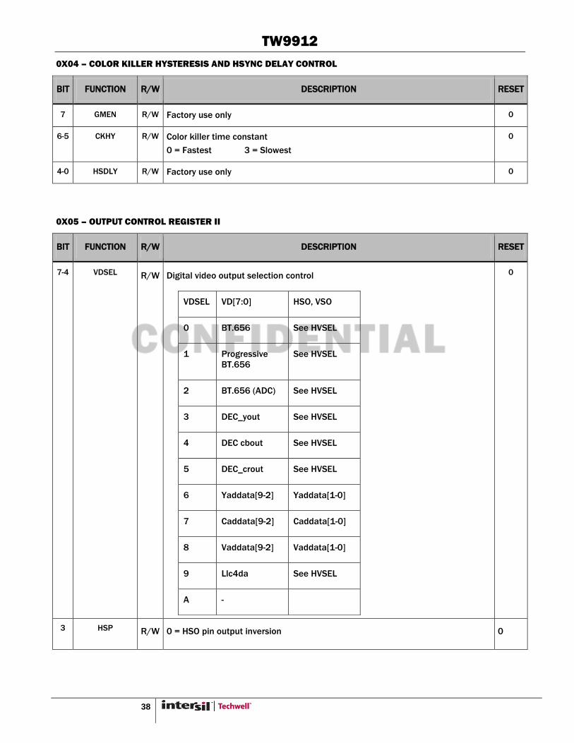
0X04 – COLOR KILLER HYSTERESIS AND HSYNC DELAY CONTROL
BIT FUNCTION R/W DESCRIPTION RESET
7 GMEN R/W Factory use only 0
6-5 CKHY R/W Color killer time constant
0 = Fastest 3 = Slowest
0
4-0 HSDLY R/W Factory use only 0
0X05 – OUTPUT CONTROL REGISTER II
BIT FUNCTION R/W DESCRIPTION RESET
7-4 VDSEL R/W Digital video output selection control
VDSEL VD[7:0] HSO, VSO
0 BT.656 See HVSEL
1 Progressive
BT.656
See HVSEL
2 BT.656 (ADC) See HVSEL
3 DEC_yout See HVSEL
4 DEC cbout See HVSEL
5 DEC_crout See HVSEL
6 Yaddata[9-2] Yaddata[1-0]
7 Caddata[9-2] Caddata[1-0]
8 Vaddata[9-2] Vaddata[1-0]
9 Llc4da See HVSEL
A -
0
3 HSP R/W 0 = HSO pin output inversion 0
TW9912
39
BIT FUNCTION R/W DESCRIPTION RESET
1 = HSO pin output no inversion
2 VSP R/W 0 = VSO pin output inversion
1 = VSO pin output no inversion
0
1-0 HVSEL R/W HSO, VSO output select control.
HVSEL HSO VSO
00 See HSY_SEL See VSY_SEL
01 Decoder generated HS Decoder generated VS
10 Deinterlacer HS Deinterlacer VS
11 - -
0
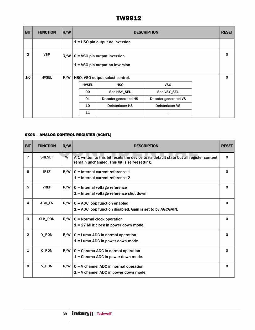
0X06 – ANALOG CONTROL REGISTER (ACNTL)
BIT FUNCTION R/W DESCRIPTION RESET
7 SRESET W A 1 written to this bit resets the device to its default state but all register content
remain unchanged. This bit is self-resetting.
0
6 IREF R/W 0 = Internal current reference 1
1 = Internal current reference 2
0
5 VREF R/W 0 = Internal voltage reference
1 = Internal voltage reference shut down
0
4 AGC_EN R/W 0 = AGC loop function enabled
1 = AGC loop function disabled. Gain is set to by AGCGAIN.
0
3 CLK_PDN R/W 0 = Normal clock operation
1 = 27 MHz clock in power down mode.
0
2 Y_PDN R/W 0 = Luma ADC in normal operation
1 = Luma ADC in power down mode.
0
1 C_PDN R/W 0 = Chroma ADC in normal operation
1 = Chroma ADC in power down mode.
0
0 V_PDN R/W 0 = V channel ADC in normal operation
1 = V channel ADC in power down mode.
0

TW9912
40
0X07 – CROPPING REGISTER, HIGH (CROP_HI)
BIT FUNCTION R/W DESCRIPTION RESET
7-6 VDELAY_HI R/W Bit[9:8] of the 10-bit Vertical Delay register 0
5-4 VACTIVE_HI R/W Bit[9:8] of the 10-bit VACTIVE register
Refer to description on Reg0x09 for its shadow register
1
3-2 HDELAY_HI R/W Bit[9:8] of the 10-bit Horizontal Delay register 0
1-0 HACTIVE_HI R/W Bit[9:8] of the 10-bit HACTIVE register 2
0X08 – VERTICAL DELAY REGISTER, LOW (VDELAY_LO)
BIT FUNCTION R/W DESCRIPTION RESET
7-0 VDELAY_LO R/W Bit[7:0] of the 10-bit Vertical Delay register. The two MSBs are in the CROP_HI
register. It defines the number of lines between the leading edge of VSYNC and
the start of the active video.
12
0X09 – VERTICAL ACTIVE REGISTER, LOW (VACTIVE_LO)
BIT FUNCTION R/W DESCRIPTION RESET
7-0 VACTIVE_LO R/W Bit[7:0] of the 10-bit Vertical Active register. The two MSBs are in the CROP_HI
register. It defines the number of active video lines per frame output.
The VACTIVE register has a shadow register for use with 50Hz source when Atreg
of Reg0x1C is not set. This register can be accessed through the same index
address by first changing the format standard to any 50Hz standard.
F0
0X0A – HORIZONTAL DELAY REGISTER, LOW (HDELAY_LO)
BIT FUNCTION R/W DESCRIPTION RESET
7-0 HDELAY_LO R/W Bit[7:0] of the 10-bit Horizontal Delay register. The two MSBs are in the CROP_HI
register. It defines the number of pixels between the leading edge of the HSYNC
and the start of the image cropping for active video.
The HDELAY_LO register has two shadow registers for use with PAL and SECAM
sources respectively. These register can be accessed using the same index
address by first changing the decoding format to the corresponding standard.
10
TW9912
41
0X0B – HORIZONTAL ACTIVE REGISTER, LOW (HACTIVE_LO)
BIT FUNCTION R/W DESCRIPTION RESET
7-0 HACTIVE_LO R/W Bit[7:0] of the 10-bit Horizontal Active register. The two MSBs are in the
CROP_HI register. It defines the number of active pixels per line output.
It is recommended to use the setting of 0x176 and 0x170 for 480p and 576p
input, respectively.
D0
0X0C – CONTROL REGISTER I (CNTRL1)
BIT FUNCTION R/W DESCRIPTION RESET
7 PBW R/W Combined with VTL[3], there are four different chroma bandwidth can be
selected
1 = Wide Chroma BPF BW
0 = Normal Chroma BPF BW
1
6 DEM R/W Color killer sensitivity
1 = Low 0 = High
1
5 PALSW R/W 1 = PAL switch sensitivity low
0 = PAL switch sensitivity normal
0
4 SET7 R/W 1 = The black level is 7.5 IRE above the blank level
0 = The black level is the same as the blank level
0
3 COMB R/W 1 = Adaptive comb filter on for NTSC/PAL
0 = Notch filter
1
2 HCOMP R/W 1 = Operation mode 1. (recommended)
0 = Operation mode 0
1
1 YCOMB R/W This bit controls the comb operation when there is no color burst
1 = No comb 0 = Comb.
0
0 PDLY R/W PAL delay line
1 = Disable 0 = Enable 0
0X0D – CC/WSS CONTROL
BIT FUNCTION R/W DESCRIPTION RESET
7 R/W Reserved 0
TW9912
42
BIT FUNCTION R/W DESCRIPTION RESET
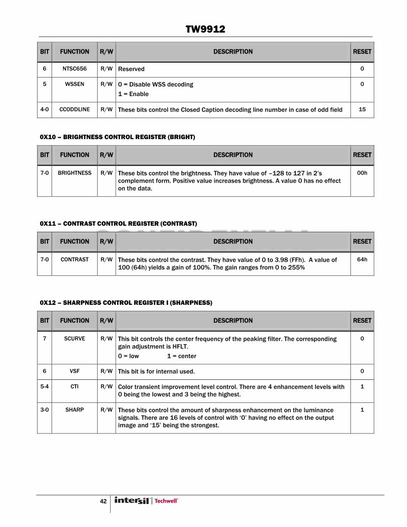
6 NTSC656 R/W Reserved 0
5 WSSEN R/W 0 = Disable WSS decoding
1 = Enable
0
4-0 CCODDLINE R/W These bits control the Closed Caption decoding line number in case of odd field 15
0X10 – BRIGHTNESS CONTROL REGISTER (BRIGHT)
BIT FUNCTION R/W DESCRIPTION RESET
7-0 BRIGHTNESS R/W These bits control the brightness. They have value of –128 to 127 in 2‘s
complement form. Positive value increases brightness. A value 0 has no effect
on the data.
00h
0X11 – CONTRAST CONTROL REGISTER (CONTRAST)
BIT FUNCTION R/W DESCRIPTION RESET
7-0 CONTRAST R/W These bits control the contrast. They have value of 0 to 3.98 (FFh). A value of
100 (64h) yields a gain of 100%. The gain ranges from 0 to 255%
64h
0X12 – SHARPNESS CONTROL REGISTER I (SHARPNESS)
BIT FUNCTION R/W DESCRIPTION RESET
7 SCURVE R/W This bit controls the center frequency of the peaking filter. The corresponding
gain adjustment is HFLT.
0 = low 1 = center
0
6 VSF R/W This bit is for internal used. 0
5-4 CTI R/W Color transient improvement level control. There are 4 enhancement levels with
0 being the lowest and 3 being the highest.
1
3-0 SHARP R/W These bits control the amount of sharpness enhancement on the luminance
signals. There are 16 levels of control with ‗0‘ having no effect on the output
image and ‗15‘ being the strongest.
1
TW9912
43
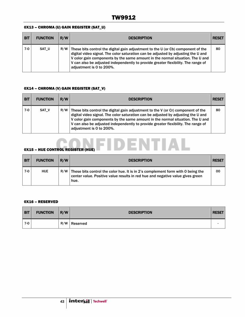
0X13 – CHROMA (U) GAIN REGISTER (SAT_U)
BIT FUNCTION R/W DESCRIPTION RESET
7-0 SAT_U R/W These bits control the digital gain adjustment to the U (or Cb) component of the
digital video signal. The color saturation can be adjusted by adjusting the U and
V color gain components by the same amount in the normal situation. The U and
V can also be adjusted independently to provide greater flexibility. The range of
adjustment is 0 to 200%.
80
0X14 – CHROMA (V) GAIN REGISTER (SAT_V)
BIT FUNCTION R/W DESCRIPTION RESET
7-0 SAT_V R/W These bits control the digital gain adjustment to the V (or Cr) component of the
digital video signal. The color saturation can be adjusted by adjusting the U and
V color gain components by the same amount in the normal situation. The U and
V can also be adjusted independently to provide greater flexibility. The range of
adjustment is 0 to 200%.
80
0X15 – HUE CONTROL REGISTER (HUE)
BIT FUNCTION R/W DESCRIPTION RESET
7-0 HUE R/W These bits control the color hue. It is in 2‘s complement form with 0 being the
center value. Positive value results in red hue and negative value gives green
hue.
00
0X16 – RESERVED
BIT FUNCTION R/W DESCRIPTION RESET
7-0 R/W Reserved -

TW9912
44
0X17 – VERTICAL PEAKING CONTROL I
BIT FUNCTION R/W DESCRIPTION RESET
7-4 SHCOR R/W These bits provide coring function for the sharpness control 3
3 R/W Reserved -
2-0 VSHP R/W Vertical peaking gain control 0
0X18 – CORING CONTROL REGISTER (CORING)
BIT FUNCTION R/W DESCRIPTION RESET
7-6 CTCOR R/W These bits control the coring function for the CTI. It has internal step size of 2 1
5-4 CCOR R/W These bits control the low level coring function for the Cb/Cr output 0
3-2 VCOR R/W These bits control the coring function of the vertical peaking logic. It has an
internal step size of 2.
1
1-0 CIF R/W These bits control the IF compensation level
0 = None 1 = 1.5 dB 2 = 3 dB 3 = 6 dB
0
0X19 – RESERVED
BIT FUNCTION R/W DESCRIPTION RESET
2-0 RTSEL R/W Reserved 0
TW9912
45
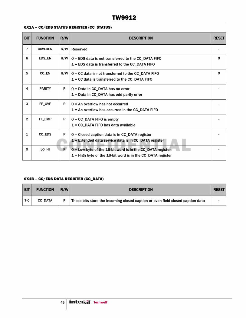
0X1A – CC/EDS STATUS REGISTER (CC_STATUS)
BIT FUNCTION R/W DESCRIPTION RESET
7 CCVLDEN R/W Reserved -
6 EDS_EN R/W 0 = EDS data is not transferred to the CC_DATA FIFO
1 = EDS data is transferred to the CC_DATA FIFO
0
5 CC_EN R/W 0 = CC data is not transferred to the CC_DATA FIFO
1 = CC data is transferred to the CC_DATA FIFO
0
4 PARITY R 0 = Data in CC_DATA has no error
1 = Data in CC_DATA has odd parity error
-
3 FF_OVF R 0 = An overflow has not occurred
1 = An overflow has occurred in the CC_DATA FIFO
-
2 FF_EMP R 0 = CC_DATA FIFO is empty
1 = CC_DATA FIFO has data available
-
1 CC_EDS R 0 = Closed caption data is in CC_DATA register
1 = Extended data service data is in CC_DATA register
-
0 LO_HI R 0 = Low byte of the 16-bit word is in the CC_DATA register
1 = High byte of the 16-bit word is in the CC_DATA register
-
0X1B – CC/EDS DATA REGISTER (CC_DATA)
BIT FUNCTION R/W DESCRIPTION RESET
7-0 CC_DATA R These bits store the incoming closed caption or even field closed caption data -

TW9912
46
0X1C – STANDARD SELECTION (SDT)
BIT FUNCTION R/W DESCRIPTION RESET
7 DETSTUS R 0 = Idle 1 = detection in progress -
6-4 STDNOW R Current standard invoked
0 = NTSC(M) 1 = PAL (B,D,G,H,I) 2 = SECAM 3 = NTSC4.43
4 = PAL (M) 5 = PAL (CN) 6 = PAL 60 7 = N/A
-
3 ATREG R/W 1 = Disable the shadow registers.
0 = Enable VACTIVE and HDELAY shadow registers value depending on standard
0
2-0 STANDARD R/W Standard selection
0 = NTSC(M) 1 = PAL (B,D,G,H,I) 2 = SECAM 3 = NTSC4.43
4 = PAL (M) 5 = PAL (CN) 6 = PAL 60 7 = Auto detection
7
0X1D – STANDARD RECOGNITION (SDTR)
BIT FUNCTION R/W DESCRIPTION RESET
7 ATSTART R/W Writing 1 to this bit will manually initiate the auto format detection process. This
bit is a self-resetting bit.
0
6 PAL6_EN R/W 1 = enable recognition of PAL60
0 = disable recognition
1
5 PALN_EN R/W 1 = enable recognition of PAL (CN)
0 = disable recognition
1
4 PALM_EN R/W 1 = enable recognition of PAL (M)
0 = disable recognition
1
3 NT44_EN R/W 1 = enable recognition of NTSC 4.43
0 = disable recognition
1
2 SEC_EN R/W 1 = enable recognition of SECAM
0 = disable recognition
1
1 PALB_EN R/W 1 = enable recognition of PAL (B,D,G,H,I)
0 = disable recognition
1
0 NTSC_EN R/W 1 = enable recognition of NTSC (M)
0 = disable recognition
1

TW9912
47
0X1E – COMPONENT VIDEO FORMAT (CVFMT)
BIT FUNCTION R/W DESCRIPTION RESET
7 NT50 R/W Set for NTSC 50Hz decoding. The STANDARD has to be in NTSC mode. 0
6-4 CVSTD R Component video input format detection
0 = 480i 1 = 576i 2 = 480p 3 = 576p others = NA
-
3-0 CVFMT R/W Component video format selection
0 = 480i 1 = 576i 2 = 480p 3 = 576p 8 = Auto others = N/A
8
0X1F – RESERVED
BIT FUNCTION R/W DESCRIPTION RESET
7-0 R/W 00h = Normal mode
01h = Analog test mode
04h = Digital test mode
0Bh = Clamp test mode
0Ch = MBIST test mode
0
0X20 – CLAMPING GAIN (CLMPG)
BIT FUNCTION R/W DESCRIPTION RESET
7-4 CLPEND R/W These 4 bits set the end time of the clamping pulse in the increment of 8 system
clocks. The clamping time is determined by this together with CLPST.
5
3-0 CLPST R/W These 4 bits set the start time of the clamping pulse in the increment of 8
system clocks. It is referenced to PCLAMP position.
0
0X21 – INDIVIDUAL AGC GAIN (IAGC)
BIT FUNCTION R/W DESCRIPTION RESET
7-4 NMGAIN R/W These bits control the normal AGC loop maximum correction value 4
3-1 WPGAIN R/W Peak AGC loop gain control 1
0 AGCGAIN8 R/W This bit is the MSB of the 9-bit register that controls the AGC gain when AGC loop
is disabled
0

TW9912
48
0X22 – AGC GAIN (AGCGAIN)
BIT FUNCTION R/W DESCRIPTION RESET
7-0 AGCGAIN R/W These bits are the lower 8 bits of the 9-bit register that controls the AGC gain
when AGC loop is disabled
F0
0X23 – WHITE PEAK THRESHOLD (PEAKWT)
BIT FUNCTION R/W DESCRIPTION RESET
7-0 PEAKWT R/W These bits control the white peak detection threshold D8
0X24– CLAMP LEVEL (CLMPL)
BIT FUNCTION R/W DESCRIPTION RESET
7 CLMPLD R/W 0 = Clamping level is set by CLMPL
1 = Clamping level preset at 60d
1
6-0 CLMPL R/W These bits determine the clamping level of the Y channel 3C
0X25– SYNC AMPLITUDE (SYNCT)
BIT FUNCTION R/W DESCRIPTION RESET
7 SYNCTD R/W 0 = Reference sync amplitude is set by SYNCT
1 = Reference sync amplitude is preset to 38h
1
6-0 SYNCT R/W These bits determine the standard sync pulse amplitude for AGC reference 38
0X26 – SYNC MISS COUNT REGISTER (MISSCNT)
BIT FUNCTION R/W DESCRIPTION RESET
7-4 MISSCNT R/W These bits set the threshold for horizontal sync miss count threshold 4
3-0 HSWIN R/W These bits set the size for the horizontal sync detection window 4

TW9912
49
0X27 – CLAMP POSITION REGISTER (PCLAMP)
BIT FUNCTION R/W DESCRIPTION RESET
7-0 PCLAMP R/W These bits set the clamping position from the PLL sync edge 38
0X28 – VERTICAL CONTROL I
BIT FUNCTION R/W DESCRIPTION RESET
7-6 VLCKI R/W Vertical lock in time.
0 = Fastest 3 = Slowest
0
5-4 VLCKO R/W Vertical lock out time.
0 = Fastest 3 = Slowest
0
3 VMODE R/W Vertical detection window.
0 = Vertical countdown mode
1 = Search mode
0
2 DETV R/W 0 = Normal Vsync logic
1 = recommended for special application only
0
1 AFLD R/W Auto field generation control
0 = Off 1 = On
0
0 VINT R/W Vertical integration time control
0 = Short 1 = Normal
0
0X29 – VERTICAL CONTROL II
BIT FUNCTION R/W DESCRIPTION RESET
7-5 BSHT R/W Burst PLL center frequency control 0
4-0 VSHT R/W Vsync output delay control in the increment of half line length 00
TW9912
50
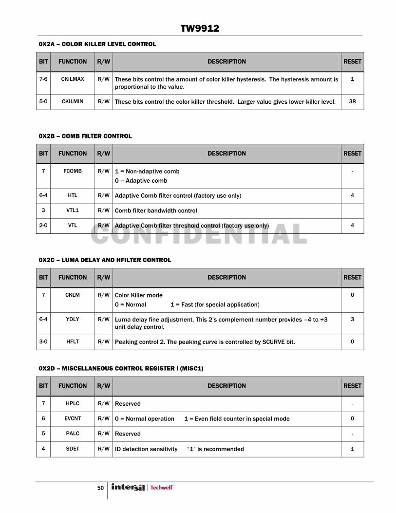
0X2A – COLOR KILLER LEVEL CONTROL
BIT FUNCTION R/W DESCRIPTION RESET
7-6 CKILMAX R/W These bits control the amount of color killer hysteresis. The hysteresis amount is
proportional to the value.
1
5-0 CKILMIN R/W These bits control the color killer threshold. Larger value gives lower killer level. 38
0X2B – COMB FILTER CONTROL
BIT FUNCTION R/W DESCRIPTION RESET
7 FCOMB R/W 1 = Non-adaptive comb
0 = Adaptive comb
-
6-4 HTL R/W Adaptive Comb filter control (factory use only) 4
3 VTL1 R/W Comb filter bandwidth control
2-0 VTL R/W Adaptive Comb filter threshold control (factory use only) 4
0X2C – LUMA DELAY AND HFILTER CONTROL
BIT FUNCTION R/W DESCRIPTION RESET
7 CKLM R/W Color Killer mode
0 = Normal 1 = Fast (for special application)
0
6-4 YDLY R/W Luma delay fine adjustment. This 2‘s complement number provides –4 to +3
unit delay control.
3
3-0 HFLT R/W Peaking control 2. The peaking curve is controlled by SCURVE bit. 0
0X2D – MISCELLANEOUS CONTROL REGISTER I (MISC1)
BIT FUNCTION R/W DESCRIPTION RESET
7 HPLC R/W Reserved -
6 EVCNT R/W 0 = Normal operation 1 = Even field counter in special mode 0
5 PALC R/W Reserved -
4 SDET R/W ID detection sensitivity ―1‖ is recommended 1

TW9912
51
BIT FUNCTION R/W DESCRIPTION RESET
3 Oplmt R/W 0 = full data output 1 = data output limited to Y=16~235 and
Cb/Cr=16~240 0
2 BYPASS R/W It controls the standard detection and should be set to ‗1‘ in normal use 1
1 SYOUT R/W 0 = Hsync is always generated
1 = Hsync is disabled when video loss is detected 0
0 HADV R/W Reserved -
0X2E – MISCELLANEOUS CONTROL REGISTER II (MISC2)
BIT FUNCTION R/W DESCRIPTION RESET
7-6 HPM R/W Horizontal PLL acquisition time.
0 = Slow 1 = Medium 2 = Auto 3 = Fast 2
5-4 ACCT R/W ACC time constant
0 = No ACC 1 = Slow 2 = Medium 3 = fast 2
3-2 SPM R/W Burst PLL control.
0 = Slowest 1 = Slow 2 = Fast 3 = Fastest 1
1-0 CBW R/W Chroma low pass filter bandwidth control.
0 = Low 1 = Medium 2 = High 3 = NA 1

TW9912
52
0X2F – MISCELLANEOUS CONTROL III (MISC3)
BIT FUNCTION R/W DESCRIPTION RESET
7 NKILL R/W 1 = Enable noisy signal color killer function in NTSC mode
0 = Disable
1
6 PKILL R/W 1 = Enable automatic noisy color killer function in PAL mode
0 = Disable
1
5 SKILL R/W 1 = Enable automatic noisy color killer function in SECAM mode
0 = Disable
1
4 CBAL R/W 0 = Normal output
1 = special output mode
0
3 FCS R/W 1 = Force decoder output value determined by CCS
0 = Disable
0
2 LCS R/W 1 = Enable pre-determined output value indicated by CCS when video loss is
detected
0 = Disable
0
1 CCS R/W When FCS is set high or video loss condition is detected when LCS is set high,
one of two colors display can be selected
1 = Blue color
0 = Black
0
0 BST R/W 1 = Enable blue stretch
0 = Disable
0
0X30 – COPY PROTECTION DETECTION
BIT FUNCTION R/W DESCRIPTION RESET
7 SID_FAIL R 1 = SECAM ID detection failed -
6 PID_FAIL R 1 = PAL ID detection failed -
5 FSC_FAIL R 1 = Fsc frequency detection failed -
4 SLOCK_FAIL R 1 = Sub-carrier lock detection failed -
3 CSBAD R 1 = color stripe detection may be un-reliable -
2 MCVSN R 1 = AGC copy protected pulse detected
0 = Not detected
-

TW9912
53
BIT FUNCTION R/W DESCRIPTION RESET
1 CSTRIPE R 1 = color stripe copy protection burst detected
0 = Not detected
-
0 CTYPE R This bit is valid only when color stripe protection is detected, i.e. CSTRIPE=1
1 = Type 2 color stripe protection
0 = Type 3 color stripe protection
-
0X31 – CHIP STATUS II (CSTATUS2)
BIT FUNCTION R/W DESCRIPTION RESET
7 VCR R VCR signal indicator -
6 WKAIR R Weak signal indicator 2 -
5 WKAIR1 R Weak signal indicator1 -
4 VSTD R Standard line per field indicator -
3 NINTL R Non-interlaced signal indicator -
2 WSSDET R 1 = WSS data detected 0 = Not detected -
1 EDSDET R 1 = EDS data detected 0 = Not detected -
0 CCDET R 1 = CC data detected 0 = Not detected -
0X32 – H MONITOR (HFREF)
BIT FUNCTION R/W DESCRIPTION RESET
7-0 HFREF, etc. R Horizontal line frequency indicator
HREF[9:2] / GVAL[8:1] / PHERRDO / CGAINO / BAMPO / MINAVG / SYTHRD /
SYAMP
-

TW9912
54
0X33 – CLAMP MODE(CLMD)
BIT FUNCTION R/W DESCRIPTION RESET
7-6 FRM R/W Free run mode
0/1 = Auto mode 2 = 60 Hz 3 = 50 Hz 0
5-4 YNR R/W Y HF Noise Reduction.
0 = None 1 = Smallest 2 = Small 3 = Medium 0
3-2 CLMD R/W Clamping mode control.
0 = Sync top 1 = Auto 2 = Pedestal 3 = NA 1
1-0 PSP R/W Slice level.
0 = Low 1 = Medium 2 = High 3 = NA 1
0X34 – ID DETECTION CONTROL (NSEN/SSEN/PSEN/WKTH)
BIT FUNCTION R/W DESCRIPTION RESET
7-6 INDEX R/W These two bits indicate which of the four lower 6-bit registers is currently being
controlled. The write sequence is a two steps process unless the same register
is written. A write of {ID,000000} selects one of the four registers to be written.
A subsequent write will actually write into the register.
0
5-0 NSEN/
SSEN /
PSEN /
WKTH
R/W IDX = 0 controls the NTSC ID detection sensitivity (NSEN)
IDX = 1 controls the SECAM ID detection sensitivity (SSEN)
IDX = 2 controls the PAL ID detection sensitivity (PSEN)
IDX = 3 controls the weak signal detection sensitivity (WKTH)
1A/
20 /
1C /
2A

TW9912
55
0X35 – CLAMP CONTROL (CLCNTL)
BIT FUNCTION R/W DESCRIPTION RESET
7 CTEST R/W Clamping control for debug use 0
6 YCLEN R/W 0 = Enable Y channel clamp
1 = Disable
0
5 CCLEN R/W 0 = Enable C channel clamp
1 = Disable
0
4 VCLEN R/W 0 = Enable V channel clamp
1 = Disable
0
3 GTEST R/W 0 = Normal operation
1 = Test
0
2 VLPF R/W Sync filter bandwidth control 0
1 CKLY R/W Clamping current control 1 0
0 CKLC R/W Clamping current control 2 0
0X36 – DE-INTERLACER CONTROL
BIT FUNCTION R/W DESCRIPTION RESET
3-2 CODD R/W Odd field offset control 0
1-0 CEVEN R/W Even field offset control 3
0X37 – DE-INTERLACER H DELAY CONTROL
BIT FUNCTION R/W DESCRIPTION RESET
7-0 HDELAY2 R/W De-interlacer capture start control 28

TW9912
56
0X38 – DE-INTERLACER SYNC GENERATION
BIT FUNCTION R/W DESCRIPTION RESET
7-0 HSTART R/W De-interlacer H sync output position control AF
0X40 – WSS0
BIT FUNCTION R/W DESCRIPTION RESET
7-6 R/W -
5-0 WSS0 R These are the sliced WSS data bit 19 to 14 -
0X41 – WSS1
BIT FUNCTION R/W DESCRIPTION RESET
7 CRCERR R This is the CRC error indicator for 525-line WSS
0 = No CRC error 1 = CRC error
-
6 WSSFLD R These bit indicates the detected WSS field information
0 = Odd 1 = Even
-
5-0 WSS1 R These bits represent the sliced WSS data bit 13 to 8 -
0X42 – WSS2
BIT FUNCTION R/W DESCRIPTION RESET
7-0 WSS2 R These bits represent the sliced WSS bit 7 to 0 -
0X43 – CCEVENLINE
BIT FUNCTION R/W DESCRIPTION RESET
4-0 CCEVENLINE R/W CC decoding line control 15

TW9912
57
ADC/PLL CONFIGURATION REGISTERS
0XC0 – LLPLL INPUT CONTROL REGISTER
BIT FUNCTION R/W DESCRIPTION RESET
7-6 INP_SEL R/W 0 = SOYIN 1~3 = not used 0
5 CS_INV R/W Polarity control for Csync detection circuitry. An active low is needed
0 = No Inversion
1 = Inversion
0
4 CS_SEL R/W PLL reference input selection
0 = Slicer or HSYNC
1 = CS_PAS
0
3 SOG_SEL R/W CSYNC source selection
0 = SOG Slicer
1 = HSYNC
0
2 HS_POL R/W PLL reference input polarity
0 = Inversion
1 = Normal
0
1 R/W Reserved -
0 CK_SEL R/W ADC clock selection
0 = Select PLL clock
1 = Select oscillator clock
0
0XC1 – LLPLL INPUT DETECTION REGISTER
BIT FUNCTION R/W DESCRIPTION RESET
7 VS_POL R Detected VSYNC polarity 0 = Low active -
6 HS_POL R Detected HSYNC polarity 0 = Low active -
5 VS_DET R VSYNC pulse detection status, 1 = detected -
4 HS_DET R HSYNC pulse detection status -
3 CS_DET R Composite Sync detection status -
2-0 DET_FMT R Input source format detection in the case of composite sync
0 = 480i 1 = 576i 2 = 480p 3 = 576p
4 = 1080i 5 = 720p 6 = 1080p 7 = none of above
-

TW9912
58
0XC2 – LLPLL CONTROL REGISTER
BIT FUNCTION R/W DESCRIPTION RESET
7-6 LLC_POST R/W Post divider control
0 = 1/8 1 = ¼ 2 = ½ 3 = 1
0
5-4 LLC_VCO R/W VCO range select (MHz)
0 = 5 ~ 27MHz 2 = 20 ~ 108MHz
1 = 10 ~ 54 MHz 3 = 40 ~ 216MHz
0
3 R/W Reserved -
2-0 LLC_IPMP R/W Charge pump currents (uA)
0 = 1.5 1 = 2.5 2 = 5 3 = 10
4 = 20 5 = 40 6 = 80 7 = 160
1
0XC3 – LLPLL DIVIDER HIGH REGISTER
BIT FUNCTION R/W DESCRIPTION RESET
7-4 R/W Reserved -
3-0 PLL_ACKN[11:8] R/W PLL feedback divider. A 12-bit register. 3
0XC4 – LLPLL DIVIDER LOW REGISTER
BIT FUNCTION R/W DESCRIPTION RESET
7-0 PLL_ACKN[7:0] R/W PLL feedback divider. A 12-bit register. 5A
0XC5 – LLPLL CLOCK PHASE REGISTER
BIT FUNCTION R/W DESCRIPTION RESET
7-5 R/W Reserved -
4-0 LLC_PHA R/W This 5-bit value adjusts the sampling phase in 32 steps across on pixel
time. Each step represents an 11.25 degree shift in sampling phase.
00
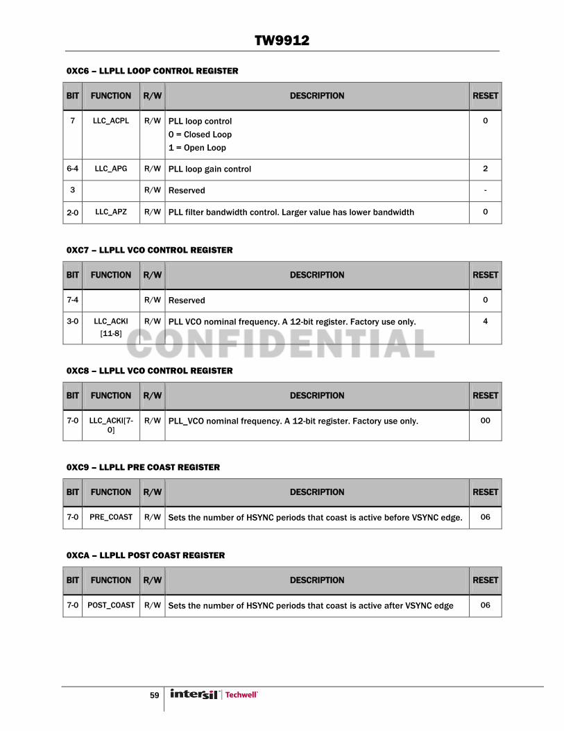
TW9912
59
0XC6 – LLPLL LOOP CONTROL REGISTER
BIT FUNCTION R/W DESCRIPTION RESET
7 LLC_ACPL R/W PLL loop control
0 = Closed Loop
1 = Open Loop
0
6-4 LLC_APG R/W PLL loop gain control 2
3 R/W Reserved -
2-0 LLC_APZ R/W PLL filter bandwidth control. Larger value has lower bandwidth 0
0XC7 – LLPLL VCO CONTROL REGISTER
BIT FUNCTION R/W DESCRIPTION RESET
7-4 R/W Reserved 0
3-0 LLC_ACKI
[11-8]
R/W PLL VCO nominal frequency. A 12-bit register. Factory use only. 4
0XC8 – LLPLL VCO CONTROL REGISTER
BIT FUNCTION R/W DESCRIPTION RESET
7-0 LLC_ACKI[7-
0]
R/W PLL_VCO nominal frequency. A 12-bit register. Factory use only. 00
0XC9 – LLPLL PRE COAST REGISTER
BIT FUNCTION R/W DESCRIPTION RESET
7-0 PRE_COAST R/W Sets the number of HSYNC periods that coast is active before VSYNC edge. 06
0XCA – LLPLL POST COAST REGISTER
BIT FUNCTION R/W DESCRIPTION RESET
7-0 POST_COAST R/W Sets the number of HSYNC periods that coast is active after VSYNC edge 06
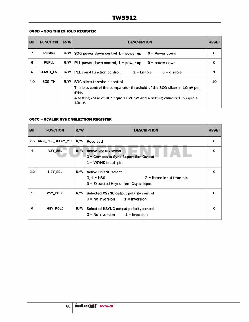
TW9912
60
0XCB – SOG THRESHOLD REGISTER
BIT FUNCTION R/W DESCRIPTION RESET
7 PUSOG R/W SOG power down control 1 = power up 0 = Power down 0
6 PUPLL R/W PLL power down control, 1 = power up 0 = power down 0
5 COAST_EN R/W PLL coast function control. 1 = Enable 0 = disable 1
4-0 SOG_TH R/W SOG slicer threshold control
This bits control the comparator threshold of the SOG slicer in 10mV per
step.
A setting value of 00h equals 320mV and a setting value is 1Fh equals
10mV.
10
0XCC – SCALER SYNC SELECTION REGISTER
BIT FUNCTION R/W DESCRIPTION RESET
7-5 RGB_CLK_DELAY_CTL R/W Reserved 0
4 VSY_SEL R/W Active VSYNC select
0 = Composite Sync Separation Output
1 = VSYNC input pin
0
3-2 HSY_SEL R/W Active HSYNC select
0, 1 = HSO 2 = Hsync input from pin
3 = Extracted Hsync from Csync input
0
1 VSY_POLC R/W Selected VSYNC output polarity control
0 = No inversion 1 = Inversion
0
0 HSY_POLC R/W Selected HSYNC output polarity control
0 = No inversion 1 = Inversion
0

TW9912
61
0XCD – PLL INITIALIZATION REGISTER
BIT FUNCTION R/W DESCRIPTION RESET
7-6 CP_X4 R/W CP_X4 selection for LLPLL 1
5-4 LP_X4 R/W LP_X4 selection for LLPLL 1
3-2 LP_X8 R/W LP_X8 selection for LLPLL 1
1 CLK_PHASE R/W ADCCLK Phase 0
0 INIT R/W PLL initialization, self-resetting 0
0XD0 –GAIN CONTROL REGISTER
BIT FUNCTION R/W DESCRIPTION RESET
7-3 Reserved R/W Reserved -
2 GAINY[8] R/W Y channel gain adjustment. Bit 8 of a 9-bit register 0
1 GAINC[8] R/W C channel gain adjustment. Bit 8 of a 9-bit register 0
0 GAINV[8] R/W V channel gain adjustment. Bit 8 of a 9-bit register 0
0XD1 – Y CHANNEL GAIN ADJUST REGISTER
BIT FUNCTION R/W DESCRIPTION RESET
7-0 GAINY[7-0] R/W Y channel gain adjustment. Bit 7 to 0 of a 9-bit register F0
0XD2 – C CHANNEL GAIN ADJUST REGISTER
BIT FUNCTION R/W DESCRIPTION RESET
7-0 GAINYC7-0] R/W C channel gain adjustment. Bit 7 to 0 of a 9-bit register F0
0XD3 – V CHANNEL GAIN ADJUST REGISTER
BIT FUNCTION R/W DESCRIPTION RESET
7-0 GAINV[7-0] R/W V channel gain adjustment. Bit 7 to 0 of a 9-bit register F0
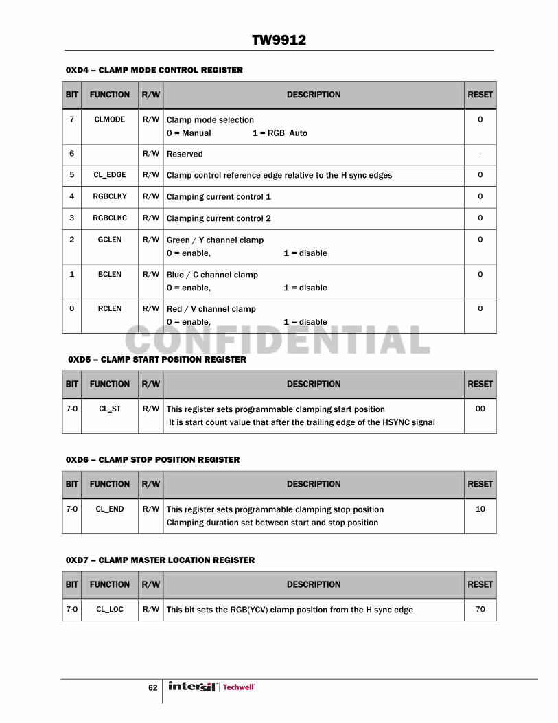
TW9912
62
0XD4 – CLAMP MODE CONTROL REGISTER
BIT FUNCTION R/W DESCRIPTION RESET
7 CLMODE R/W Clamp mode selection
0 = Manual 1 = RGB Auto
0
6 R/W Reserved -
5 CL_EDGE R/W Clamp control reference edge relative to the H sync edges 0
4 RGBCLKY R/W Clamping current control 1 0
3 RGBCLKC R/W Clamping current control 2 0
2 GCLEN R/W Green / Y channel clamp
0 = enable, 1 = disable
0
1 BCLEN R/W Blue / C channel clamp
0 = enable, 1 = disable
0
0 RCLEN R/W Red / V channel clamp
0 = enable, 1 = disable
0
0XD5 – CLAMP START POSITION REGISTER
BIT FUNCTION R/W DESCRIPTION RESET
7-0 CL_ST R/W This register sets programmable clamping start position
It is start count value that after the trailing edge of the HSYNC signal
00
0XD6 – CLAMP STOP POSITION REGISTER
BIT FUNCTION R/W DESCRIPTION RESET
7-0 CL_END R/W This register sets programmable clamping stop position
Clamping duration set between start and stop position
10
0XD7 – CLAMP MASTER LOCATION REGISTER
BIT FUNCTION R/W DESCRIPTION RESET
7-0 CL_LOC R/W This bit sets the RGB(YCV) clamp position from the H sync edge 70

TW9912
63
0XD8 – ADC TEST REGISTER
BIT FUNCTION R/W DESCRIPTION RESET
6-4 LLC_DBG_SEL R/W Debugging register for internal use 0
3 R/W Reserved -
2 R/W Reserved 0
1 R/W Reserved 0
0 R/W Reserved 0
0XD9 – Y CLAMP REFERENCE REGISTER
BIT FUNCTION R/W DESCRIPTION RESET
7-0 CL_Y_VAL R/W Green / Y channel clamping reference level in programmable mode 04
0XDA – C CLAMP REFERENCE REGISTER
BIT FUNCTION R/W DESCRIPTION RESET
7-0 CL_C_VAL R/W Blue / U channel clamping reference level in programmable mode 80
0XDB – V CLAMP REFERENCE REGISTER
BIT FUNCTION R/W DESCRIPTION RESET
7-0 CL_V_VAL R/W Red / V channel clamping reference level in programmable mode 80
0XDC – HSO WIDTH
BIT FUNCTION R/W DESCRIPTION RESET
7 EDGE_SEL R/W Edge Select 0
6 R/W Reserved -
5-0 HS_WIDTH R/W Output HS Width in number of output clocks 20
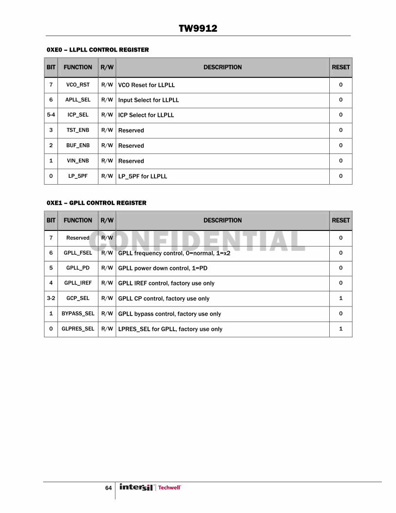
TW9912
64
0XE0 – LLPLL CONTROL REGISTER
BIT FUNCTION R/W DESCRIPTION RESET
7 VCO_RST R/W VCO Reset for LLPLL 0
6 APLL_SEL R/W Input Select for LLPLL 0
5-4 ICP_SEL R/W ICP Select for LLPLL 0
3 TST_ENB R/W Reserved 0
2 BUF_ENB R/W Reserved 0
1 VIN_ENB R/W Reserved 0
0 LP_5PF R/W LP_5PF for LLPLL 0
0XE1 – GPLL CONTROL REGISTER
BIT FUNCTION R/W DESCRIPTION RESET
7 Reserved R/W 0
6 GPLL_FSEL R/W GPLL frequency control, 0=normal, 1=x2 0
5 GPLL_PD R/W GPLL power down control, 1=PD 0
4 GPLL_IREF R/W GPLL IREF control, factory use only 0
3-2 GCP_SEL R/W GPLL CP control, factory use only 1
1 BYPASS_SEL R/W GPLL bypass control, factory use only 0
0 GLPRES_SEL R/W LPRES_SEL for GPLL, factory use only 1
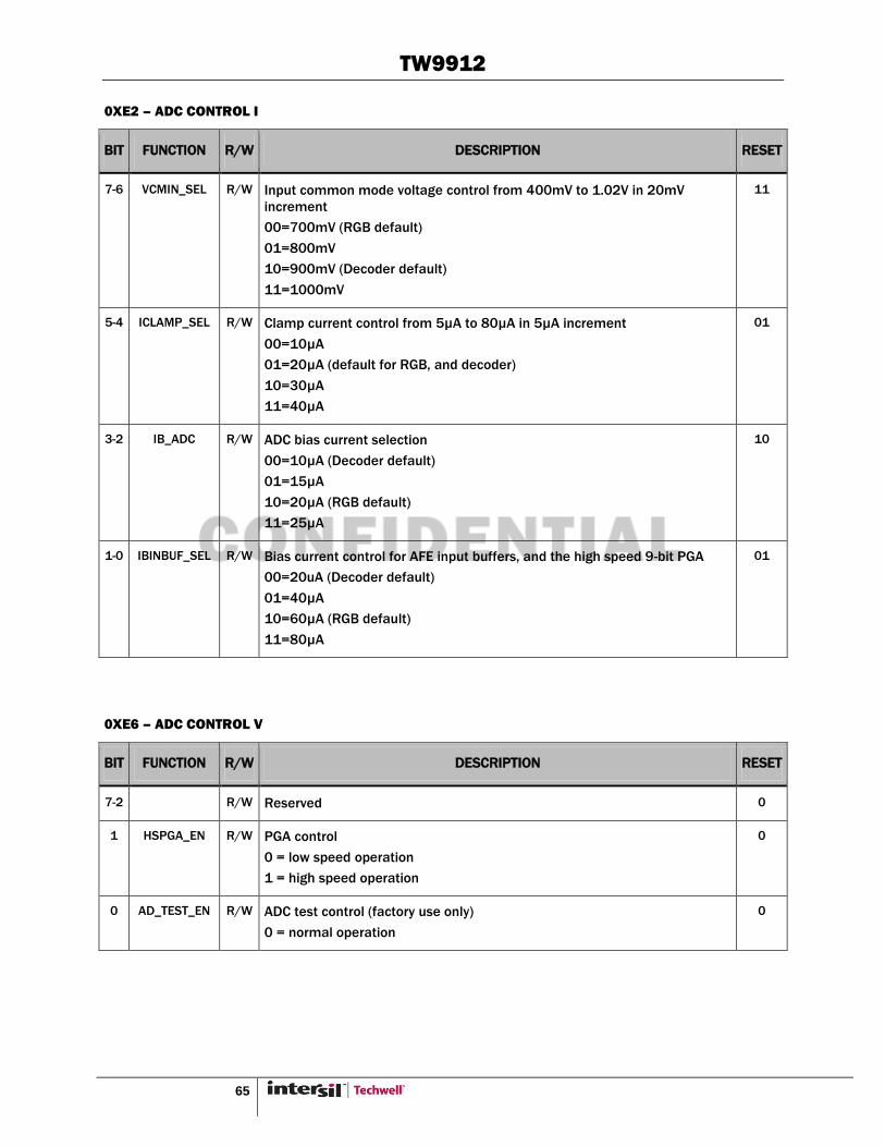
TW9912
65
0XE2 – ADC CONTROL I
BIT FUNCTION R/W DESCRIPTION RESET
7-6 VCMIN_SEL R/W Input common mode voltage control from 400mV to 1.02V in 20mV
increment
00=700mV (RGB default)
01=800mV
10=900mV (Decoder default)
11=1000mV
11
5-4 ICLAMP_SEL R/W Clamp current control from 5µA to 80µA in 5µA increment
00=10µA
01=20µA (default for RGB, and decoder)
10=30µA
11=40µA
01
3-2 IB_ADC R/W ADC bias current selection
00=10µA (Decoder default)
01=15µA
10=20µA (RGB default)
11=25µA
10
1-0 IBINBUF_SEL R/W Bias current control for AFE input buffers, and the high speed 9-bit PGA
00=20uA (Decoder default)
01=40µA
10=60µA (RGB default)
11=80µA
01
0XE6 – ADC CONTROL V
BIT FUNCTION R/W DESCRIPTION RESET
7-2 R/W Reserved 0
1 HSPGA_EN R/W PGA control
0 = low speed operation
1 = high speed operation
0
0 AD_TEST_EN R/W ADC test control (factory use only)
0 = normal operation
0
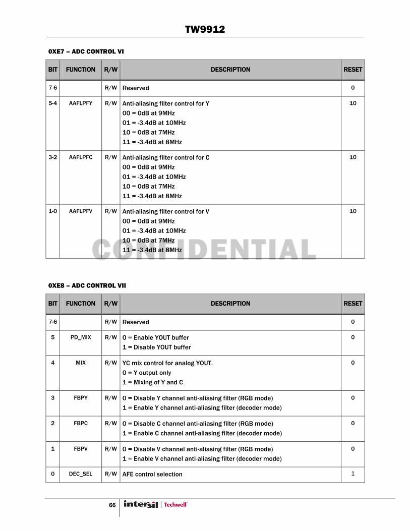
TW9912
66
0XE7 – ADC CONTROL VI
BIT FUNCTION R/W DESCRIPTION RESET
7-6 R/W Reserved 0
5-4 AAFLPFY R/W Anti-aliasing filter control for Y
00 = 0dB at 9MHz
01 = -3.4dB at 10MHz
10 = 0dB at 7MHz
11 = -3.4dB at 8MHz
10
3-2 AAFLPFC R/W Anti-aliasing filter control for C
00 = 0dB at 9MHz
01 = -3.4dB at 10MHz
10 = 0dB at 7MHz
11 = -3.4dB at 8MHz
10
1-0 AAFLPFV R/W Anti-aliasing filter control for V
00 = 0dB at 9MHz
01 = -3.4dB at 10MHz
10 = 0dB at 7MHz
11 = -3.4dB at 8MHz
10
0XE8 – ADC CONTROL VII
BIT FUNCTION R/W DESCRIPTION RESET
7-6 R/W Reserved 0
5 PD_MIX R/W 0 = Enable YOUT buffer
1 = Disable YOUT buffer
0
4 MIX R/W YC mix control for analog YOUT.
0 = Y output only
1 = Mixing of Y and C
0
3 FBPY R/W 0 = Disable Y channel anti-aliasing filter (RGB mode)
1 = Enable Y channel anti-aliasing filter (decoder mode)
0
2 FBPC R/W 0 = Disable C channel anti-aliasing filter (RGB mode)
1 = Enable C channel anti-aliasing filter (decoder mode)
0
1 FBPV R/W 0 = Disable V channel anti-aliasing filter (RGB mode)
1 = Enable V channel anti-aliasing filter (decoder mode)
0
0 DEC_SEL R/W AFE control selection 1
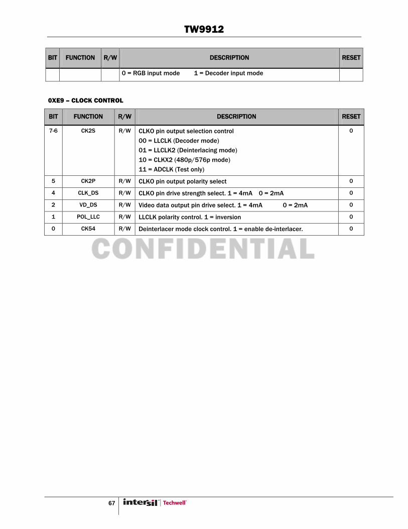
TW9912
67
BIT FUNCTION R/W DESCRIPTION RESET
0 = RGB input mode 1 = Decoder input mode
0XE9 – CLOCK CONTROL
BIT FUNCTION R/W DESCRIPTION RESET
7-6 CK2S R/W CLKO pin output selection control
00 = LLCLK (Decoder mode)
01 = LLCLK2 (Deinterlacing mode)
10 = CLKX2 (480p/576p mode)
11 = ADCLK (Test only)
0
5 CK2P R/W CLKO pin output polarity select 0
4 CLK_DS R/W CLKO pin drive strength select. 1 = 4mA 0 = 2mA 0
2 VD_DS R/W Video data output pin drive select. 1 = 4mA 0 = 2mA 0
1 POL_LLC R/W LLCLK polarity control. 1 = inversion 0
0 CK54 R/W Deinterlacer mode clock control. 1 = enable de-interlacer. 0
TW9912
For additional products, see www.intersil.com/product_tree
Intersil products are manufactured, assembled and tested utilizing ISO9000 quality systems as noted
in the quality certifications found at www.intersil.com/design/quality
Intersil products are sold by description only. Intersil Corporation reserves the right to make changes in circuit design, software and/or specifications at any time
without notice. Accordingly, the reader is cautioned to verify that data sheets are current before placing orders. Information furnished by Intersil is believed to be
accurate and reliable. However, no responsibility is assumed by Intersil or its subsidiaries for its use; nor for any infringements of patents or other rights of third
parties which may result from its use. No license is granted by implication or otherwise under any patent or patent rights of Intersil or its subsidiaries.
For information regarding Intersil Corporation and its products, see www.intersil.com
Life Support Policy These products are not authorized for use as critical components in life support devices or systems.
Datasheet Revision History
DATE NOTE
April 26, 2012 Initial Release.
August 21, 2012 Updated Ordering Information to reflect the new A3 die revision: ―TW9912-NA3-CR‖