nuc970 series datasheet -...
TRANSCRIPT

NUC970
June 01, 2015 Page 1 of 98 Rev 1.0
NU
C97
0 S
ER
IES
DA
TA
SH
EE
T
ARM® ARM926EJ-S Based
32-bit Microprocessor
NUC970 Series
Datasheet
The information described in this document is the exclusive intellectual property of Nuvoton Technology Corporation and shall not be reproduced without permission from Nuvoton.
Nuvoton is providing this document only for reference purposes of ARM926EJ-S based system design. Nuvoton assumes no responsibility for errors or omissions.
All data and specifications are subject to change without notice.
For additional information or questions, please contact: Nuvoton Technology Corporation.
www.nuvoton.com

NUC970
June 01, 2015 Page 2 of 98 Rev 1.0
NU
C97
0 S
ER
IES
DA
TA
SH
EE
T
Table of Contents
List of Figures ......................................................................................... 7
List of Tables .......................................................................................... 8
1 GENERAL DESCRIPTION .................................................................. 9
2 FEATURES ....................................................................................... 10
2.1 NUC970 Series Features ...................................................................... 10
3 PARTS INFORMATION LIST AND PIN CONFIGURATION .............. 17
3.1 NUC970 Series Part Number Naming Guide ................................................ 17
3.2 NUC970 Series Part Selection Guide ......................................................... 18
3.3 Pin Configuration ................................................................................. 20
3.3.1 NUC972DFxxY Pin Diagram ......................................................................... 20
3.3.2 NUC973DFxxY Pin Diagram ......................................................................... 21
3.3.3 NUC976DKxxY Pin Diagram ........................................................................ 22
3.3.4 NUC977DKxxY Pin Diagram ........................................................................ 23
3.4 Pin Description .................................................................................... 24
4 BLOCK DIAGRAM ............................................................................ 49
4.1 NUC970 Series Block Diagram ................................................................ 49
5 FUNCTIONAL DESCRIPTION .......................................................... 50
5.1 ARM® ARM926EJ-S CPU Core ................................................................ 50
5.1.1 Overview ................................................................................................ 50
5.2 System Manager ................................................................................. 51
5.2.1 Overview ................................................................................................ 51
5.3 Clock Controller (CLK_CTL) .................................................................... 51
5.3.1 Overview ................................................................................................ 51
5.3.2 Features ................................................................................................. 51
5.4 Advanced Interrupt Controller (AIC) ........................................................... 51
5.4.1 Overview ................................................................................................ 51
5.4.2 Features ................................................................................................. 52
5.5 SDRAM Interface Controller (SDIC) ........................................................... 52
5.5.1 Overview ................................................................................................ 52
5.5.2 Features ................................................................................................. 53
5.6 MTP Controller (MTP) ........................................................................... 53
5.6.1 Overview ................................................................................................ 53

NUC970
June 01, 2015 Page 3 of 98 Rev 1.0
NU
C97
0 S
ER
IES
DA
TA
SH
EE
T
5.6.2 Features ................................................................................................. 53
5.7 External Bus Interface (EBI) .................................................................... 53
5.7.1 Overview ................................................................................................ 53
5.7.2 Features ................................................................................................. 53
5.8 General Purpose I/O (GPIO) ................................................................... 53
5.8.1 Overview ................................................................................................ 54
5.8.2 Features ................................................................................................. 54
5.9 General DMA Controller (GDMA) .............................................................. 54
5.9.1 Overview ................................................................................................ 54
5.9.2 Features ................................................................................................. 54
5.10 Timer Controller (TMR) .......................................................................... 54
5.10.1 Overview ................................................................................................ 55
5.10.2 Features ................................................................................................. 55
5.11 Enhance Timer Controller (ETMR) ............................................................ 55
5.11.1 Overview ................................................................................................ 55
5.11.2 Features ................................................................................................. 55
5.12 Pulse Width Modulation (PWM) ................................................................ 55
5.12.1 Overview ................................................................................................ 56
5.12.2 Features ................................................................................................. 56
5.13 Watchdog Timer (WDT) ......................................................................... 56
5.13.1 Overview ................................................................................................ 56
5.13.2 Features ................................................................................................. 56
5.14 Windowed Watchdog Timer (WWDT) ......................................................... 57
5.14.1 Overview ................................................................................................ 57
5.14.2 Features ................................................................................................. 57
5.15 Real Time Clock (RTC) .......................................................................... 58
5.15.1 Overview ................................................................................................ 58
5.15.2 Features ................................................................................................. 58
5.16 UART Interface Controller (UART) ............................................................ 59
5.16.1 Overview ................................................................................................ 59
5.16.2 Features ................................................................................................. 60
5.17 Smart Card Host Interface (SC) ................................................................ 60
5.17.1 Overview ................................................................................................ 60
5.17.2 Features ................................................................................................. 60
5.18 I2C Synchronous Serial Interface Controller (I2C) ........................................... 61
NUC970
June 01, 2015 Page 4 of 98 Rev 1.0
NU
C97
0 S
ER
IES
DA
TA
SH
EE
T
5.18.1 Overview ................................................................................................ 61
5.18.2 Features ................................................................................................. 61
5.19 SPI Interface Controller (SPI) .................................................................. 62
5.19.1 Overview ................................................................................................ 62
5.19.2 Features ................................................................................................. 62
5.20 I2S Controller (I2S) ................................................................................ 62
5.20.1 Overview ................................................................................................ 62
5.20.2 Features ................................................................................................. 62
5.21 Ethernet MAC Controller (EMAC) ............................................................. 63
5.21.1 Overview ................................................................................................ 63
5.21.2 Features ................................................................................................. 63
5.22 USB 2.0 Device Controller (USBD) ............................................................ 63
5.22.1 Overview ................................................................................................ 63
5.22.2 Features ................................................................................................. 64
5.23 USB Host Controller (USBH) ................................................................... 64
5.23.1 Overview ................................................................................................ 64
5.23.2 Features ................................................................................................. 64
5.24 Controller Area Network (CAN) ................................................................ 64
5.24.1 Overview ................................................................................................ 64
5.24.2 Features ................................................................................................. 65
5.25 Flash Memory Interface (FMI) .................................................................. 65
5.25.1 Overview ................................................................................................ 65
5.25.2 Features: ................................................................................................ 65
5.26 Secure Digital Host Controller (SDH) ......................................................... 66
5.26.1 Overview ................................................................................................ 66
5.26.2 Features ................................................................................................. 66
5.27 Cryptographic Accelerator (CRYPTO) ........................................................ 67
5.27.1 Overview ................................................................................................ 67
5.27.2 Features ................................................................................................. 67
5.28 2D Graphic Engine (GE2D) ..................................................................... 68
5.28.1 Overview ................................................................................................ 68
5.28.2 Features ................................................................................................. 68
5.29 JPEG Codec (JPEG) ............................................................................ 69
5.29.1 Overview ................................................................................................ 69
5.29.2 Features ................................................................................................. 69

NUC970
June 01, 2015 Page 5 of 98 Rev 1.0
NU
C97
0 S
ER
IES
DA
TA
SH
EE
T
5.30 LCD Display Interface Controller (LCM) ...................................................... 70
5.30.1 Overview ................................................................................................ 70
5.30.2 Features ................................................................................................. 70
5.31 Capture Sensor Interface Controller (CAP) .................................................. 70
5.31.1 Overview ................................................................................................ 71
5.31.2 Feature .................................................................................................. 71
5.32 Analog to Digital Converter (ADC) ............................................................. 71
5.32.1 Overview ................................................................................................ 71
5.32.2 Features ................................................................................................. 71
5.33 Keypad Interface (KPI) .......................................................................... 72
5.33.1 Overview ................................................................................................ 72
5.33.2 Features ................................................................................................. 72
6 ELECTRICAL CHARACTERISTICS .................................................. 73
6.1 Absolute Maximum Ratings ..................................................................... 73
6.2 DC Electrical Characteristics ................................................................... 74
6.2.1 NUC970 Series DC Electrical Characteristics .................................................... 74
6.3 AC Electrical Characteristics ................................................................... 77
6.3.1 External 4~24 MHz High Speed Oscillator ........................................................ 77
6.3.2 External 4~24 MHz High Speed Crystal ........................................................... 78
6.3.3 External 32.768 kHz Low Speed Crystal ........................................................... 79
6.3.4 EBI Timing .............................................................................................. 80
6.3.5 I2C Interface Timing ................................................................................... 81
6.3.6 SPI Interface Timing................................................................................... 82
6.3.7 I2S Interface Timing ................................................................................... 83
6.3.8 Ethernet Interface Timing ............................................................................ 84
6.3.9 NAND Interface Timing ............................................................................... 86
6.3.10 SD Interface Timing ................................................................................... 87
6.3.11 LCD Display Interface Timing ........................................................................ 89
6.3.12 Capture Sensor Interface Timing .................................................................... 90
6.4 Analog Characteristics ........................................................................... 91
6.4.1 12-bit SARADC ........................................................................................ 91
6.4.2 Low Voltage Detection (LVD) and Low Voltage Reset (LVR) .................................. 92
6.4.3 3.3V Power-On Reset (POR33) ..................................................................... 93
6.4.4 1.2V Power-On Reset (POR12) ..................................................................... 93
6.4.5 USB 2.0 PHY ........................................................................................... 93
NUC970
June 01, 2015 Page 6 of 98 Rev 1.0
NU
C97
0 S
ER
IES
DA
TA
SH
EE
T
7 PACKAGE DIMENSIONS ................................................................. 95
7.1 216L LQFP (24x24x1.4mm footprint 2.0mm) ................................................ 95
7.2 128L LQFP (14x14x1.4mm footprint 2.0mm) ................................................ 96
8 REVISION HISTORY ........................................................................ 97

NUC970
June 01, 2015 Page 7 of 98 Rev 1.0
NU
C97
0 S
ER
IES
DA
TA
SH
EE
T
LIST OF FIGURES
Figure 3-1 NUC970 Series Part Number Naming Guide ............................................................... 17
Figure 3.3-1 NUC972DFxxY LQFP 216-pin Pin Diagram .............................................................. 20
Figure 3.3-2 NUC973DFxxY LQFP 216-pin Pin Diagram .............................................................. 21
Figure 3.3-3 NUC976DKxxY LQFP 128-pin Pin Diagram.............................................................. 22
Figure 3.3-4 NUC977DKxxY LQFP 128-pin Pin Diagram.............................................................. 23
Figure 6.3-1 External 4~24 MHz High Speed Oscillator Timing Diagram ..................................... 77
Figure 6.3-2 Typical HXT Crystal Application Circuit ..................................................................... 78
Figure 6.3-3 Typical LXT Crystal Application Circuit ...................................................................... 79
Figure 6.3-4 External Bus Interface Timing Diagram ..................................................................... 80
Figure 6.3-5 I2C Interface Timing Diagram .................................................................................... 81
Figure 6.3-6 SPI Interface Timing Diagram ................................................................................... 82
Figure 6.3-7 I2S Interface Timing Diagram ..................................................................................... 83
Figure 6.3-8 RMII Interface Timing Diagram .................................................................................. 84
Figure 6.3-9 Ethernet PHY Management Interface Timing Diagram ............................................. 85
Figure 6.3-10 NAND Interface Timing Diagram ............................................................................. 86
Figure 6.3-11 SD Interface Default Mode Timing Diagram ............................................................ 87
Figure 6.3-12 SD Interface High-Speed Mode Timing Diagram .................................................... 88
Figure 6.3-13 LCD Display Interface SYNC Type Timing Diagram ............................................... 89
Figure 6.3-14 Capture Sensor Interface Timing Diagram .............................................................. 90

NUC970
June 01, 2015 Page 8 of 98 Rev 1.0
NU
C97
0 S
ER
IES
DA
TA
SH
EE
T
LIST OF TABLES
No table of figures entries found.

NUC970
June 01, 2015 Page 9 of 98 Rev 1.0
NU
C97
0 S
ER
IES
DA
TA
SH
EE
T
1 GENERAL DESCRIPTION
The NUC970 series targeted for general purpose 32-bit microcontroller embeds an outstanding CPU core ARM926EJ-S, a RISC processor designed by Advanced RISC Machines Ltd., runs up to 300 MHz, with 16 KB I-cache, 16 KB D-cache and MMU, 56KB embedded SRAM and 16 KB IBR (Internal Boot ROM) for booting from USB, NAND and SPI FLASH.
The NUC970 series integrates two 10/100 Mb Ethernet MAC controllers, USB 2.0 HS HOST/Device controller with HS transceiver embedded, TFT type LCD controller, CMOS sensor I/F controller, 2D graphics engine, DES/3DES/AES crypto engine, I
2S I/F controller,
SD/MMC/NAND FLASH controller, GDMA and 8 channels 12-bit ADC controller with resistance touch screen functionality. It also integrates UART, SPI/MICROWIRE, I
2C, CAN, LIN, PWM,
Timer, WDT/Windowed-WDT, GPIO, Keypad, Smart Card I/F, 32.768 KHz XTL and RTC (Real Time Clock).
In addition, the NUC970 series integrates a memory I/F runs up to 150MHz with supporting DDR2 type SDRAM, SRAM and external device with DMA request and ack.
NUC970
June 01, 2015 Page 10 of 98 Rev 1.0
NU
C97
0 S
ER
IES
DA
TA
SH
EE
T
2 FEATURES
2.1 NUC970 Series Features
Core
– ARM® ARM926EJ-S™ processor core runs up to 300 MHz – Support 16 KB instruction cache and 16 KB data cache – Support MMU – Support JTAG Debug interface
External Bus Interface (EBI)
– Support SRAM and external I/O devices – Support 8/16-bit data bus width – Support up to five chip selects for SRAM and external I/O devices – Support programmable access cycle – Support four 32-bit write buffers
DDR SDRAM Controller
– Support DDR2 SDRAM – Clock speed up to 150 MHz – Support 16-bit data bus width – Memory size depended on embedded SDRAM configuration by different part number.
Embedded SRAM and ROM
– Support 56K bytes embedded SRAM – Support 16K bytes Internal Boot ROM (IBR) – Support up to four booting modes – Boot from USB – Boot from eMMC – Boot from NAND Flash – Boot from SPI Flash
Clock Control
– Support two PLLs, up to 500 MHz, for high performance system operation – External 12 MHz high speed crystal input for precise timing operation – External 32.768 kHz low speed crystal input for RTC function and low speed clock
source
Ethernet MAC Controller
– Support up to 2 Ethernet MAC controllers – Support IEEE Std. 802.3 CSMA/CD protocol – Support packet time stamping for IEEE Std. 1588 protocol – Support 10 and 100 Mbps operations – Support Half- and Full-duplex operations – Support RMII interface to Ethernet physical layer PHY – Support Ethernet physical layer PHY management through MDC and MDIO interface – Support flow control in Full-duplex mode to receive, recognize and transmit PAUSE
frame – Support CAM-like function to recognize 48-bit Ethernet MAC address – Support Wake-On-LAN by detecting Magic Packet – Support 256 bytes transmit FIFO and 256 bytes receive FIFO – Support DMA function – Support internal loop back mode for diagnostic
USB 2.0 Controller
– Support USB Revision 2.0 specification – Support one set of USB 2.0 High-Speed (HS) Device/Host with embedded transceiver

NUC970
June 01, 2015 Page 11 of 98 Rev 1.0
NU
C97
0 S
ER
IES
DA
TA
SH
EE
T
– Support one set of USB 2.0 High-Speed (HS) Host with embedded transceiver – Support Control, Bulk, Interrupt, Isochronous and Split transfers – Support USB host function compliant to Enhanced Host Controller Interface (EHCI) 1.0
specification to connect with USB 2.0 High-Speed (HS) device. – Support USB host function compliant to Open Host Controller Interface (OHCI) 1.0
specification to connect with USB 1.1 Full-Speed (FS) and Low-Speed (LS) devices – Support USB High-Speed (HS) and Full-Speed (FS) device function – Support USB device function with 1 endpoint for Control IN/OUT transfers and 12
programmable endpoints for Bulk, Interrupt and Isochronous IN/OUT transfers – Support suspend, resume and remote wake-up capability – Support DMA function – Support 2048 Bytes internal SRAM for USB host function and 4096 Bytes internal
SRAM for USB device function
Flash Memory Interface
– Support NAND flash interface – Support 8-bit data bus width – Support SLC and MLC type NAND flash device – Support 512 B, 2 KB, 4 KB and 8 KB page size NAND flash device – Support ECC4, ECC8, ECC12, ECC15 and ECC24 BCH algorithm for ECC code
generation, error detection and error correction. – Support eMMC flash interface – Support DMA function to accelerate the data transfer between system memory and
NAND and eMMC flash.
I2S Controller
– Support I2S interface
Support both mono and stereo Support both record and playback Support 8-bit, 16-bit 20-bit and 24-bit data precision Support master and slave mode
– Support PCM interface Support 2 slots mode to connect 2 device Support 8-bit, 16-bit 20-bit and 24-bit data precision Support master mode
– Support four 8x24 (8 24-bit) buffer for left/right channel record and left/right playback – Support DMA function to accelerate the data transfer between system memory and
internal buffer – Support 2 buffer address for left/right channel and 2 slots data transfer
LCD Display Controller
– Support 8/9/16/18/24-bit data with to connect with 80/68 series MPU type LCD module – Support resolution up to 1024x768 – Support data format conversion from RGB444, RGB565, RGB666, RGB888, YUV422
and YUV444 to RGB444, RGB565, RGB666, RGB888, YUV422 and YUV444 for display output
– Support CCIR-656 (with VSYNC, HSYNC and data enable sync signal) 8/16-bit YUV data output to connect with external TV encoder
– Support 8/16 bpp OSD data with video overlay function to facilitate the diverse graphic UI
– Support linear 1X to 8X image scaling up function – Support Picture-In-Picture display function – Support hardware cursor
Capture (CMOS Sensor Interface)
– Support CCIR601 & CCIR656 interfaces to connect with CMOS image sensor – Support resolution up to 3M pixels

NUC970
June 01, 2015 Page 12 of 98 Rev 1.0
NU
C97
0 S
ER
IES
DA
TA
SH
EE
T
– Support YUV422 and RGB565 color format for data output by CMOS image sensor – Support YUV422, RGB565, RGB555 and Y-only color format for data storing to system
memory – Support planar and packet data format for data storing to system memory – Support image cropping and the cropping window is up to 4096x2048 – Support image scaling-down: – Support vertical and horizontal scaling-down for preview mode – Support N/M scaling factor where N is equal to or less than M – Support 2 pairs of configurable 16-bit N and 16-bit M – Support to combine two interlace-fields to a single frame for data output by TV-
decoder. – Support 3 color processing effects – Negative picture – Sepia picture – Posterization
2D Graphic Engine
– Support 2D Bit Block Transfer (BitBLT) functions defined in Microsoft GDI – Support Host BLT – Support Pattern BLT – Support Color/Font Expanding BLT – Support Transparent BLT – Support Tile BLT – Support Block Move BLT – Support Copy File BLT – Support Color/Font Expansion – Support Rectangle Fill – Support RGB332/RGB565/RGB888 data format. – Support fore/background colors and all Microsoft 256 ternary raster-operation codes
(ROP) – Support both inside and outside clipping function – Support alpha-blending for source/destination picture overlaying – Support fast Bresenham line drawing algorithm to draw solid/textured line – Support rectangular border and frame drawing – Support picture re-sizing – Support down-scaling from 1/255 to 254/255 – Support up-scaling from 1 to 1.996 (1+254/255) – Support object rotation with different degree – Support L45 (45 degree left rotation) and L90 (90 degree left rotation) – Support R45 (45 degree right rotation) and R90 (90 degree right rotation) – Support M180 (mirror/flop) – Support F180 (up-side-down (flip) and X180 (180 degree rotation)
JPEG Codec
– Support Baseline Sequential mode JPEG codec function compliant with ISO/IEC 10918-1 international JPEG standard
– Planar Format – Support to encode interleaved YCbCr 4:2:2/4:2:0 and gray-level (Y only) format image – Support to decode interleaved YCbCr 4:4:4/4:2:2/4:2:0/4:1:1 and gray-level (Y only)
format image – Support to decode YCbCr 4:2:2 transpose format – Support arbitrary width and height image encode and decode – Support three programmable quantization-tables – Support standard default Huffman-table and programmable Huffman-table for decode – Support arbitrarily 1X~8X image up-scaling function for encode mode – Support down-scaling function for encode and decode modes
NUC970
June 01, 2015 Page 13 of 98 Rev 1.0
NU
C97
0 S
ER
IES
DA
TA
SH
EE
T
– Support specified window decode mode – Support quantization-table adjustment for bit-rate and quality control in encode mode – Support rotate function in encode mode – Packet Format – Support to encode interleaved YUYV format input image, output bit stream 4:2:2 and
4:2:0 format – Support to decode interleaved YCbCr 4:4:4/4:2:2/4:2:0 format image – Support decoded output image RGB555, RGB565 and RGB888 formats. – The encoded JPEG bit-stream format is fully compatible with JFIF and EXIF standards – Support arbitrary width and height image encode and decode – Support three programmable quantization-tables – Support standard default Huffman-table and programmable Huffman-table for decode – Support arbitrarily 1X~8X image up-scaling function for encode mode – Support down-scaling function 1X~ 16X for Y422 and Y420, 1X~ 8X for Y444 for
decode mode – Support specified window decode mode – Support quantization-table adjustment for bit-rate and quality control in encode mode
Crypto Engine
– PRNG – Support 64-bit, 128-bit, 192-bit and 256-bit key generation – DES – Support FIPS 46-3 – Support both encryption and decryption – Support ECB, CBC, CFB, OFB and CTR modes – 3DES – Support FIPS NIST 800-67 – Implements according to the X9.52 standard – Support 112-bit and 168-bit key – Support both encryption and decryption – Support ECB, CBC, CFB, OFB and CTR modes – AES – Support FIPS NIST 197 – Support SP800-38A & addendum – Support 128-bit, 192-bit and 256-bit key – Support both encryption and decryption – Support ECB, CBC, CFB, OFB , CTR, CBC-CS1, CBC-CS2 and CBC-CS3 modes – Support Key Expander – SHA/HMAC – Support FIPS NIST 180, 180-1, 180-2 – Support SHA-160, SHA-224, SHA-256, SHA-384, SHA-512 and corresponding HMAC
algorithm – Support 128-bit MTP key
GDMA (General DMA)
– Support 2 channels GDMA for memory-to-memory data transfer without CPU intervention
– Support increment and decrement for source and destination address calculation – Support 8-bit, 16-bit and 32-bit width data transfer – Support four 8-bit/16-bit/32-bit burst transfer
UART
– Support up to 11 UART controllers – Support 1 UART (UART 1) port with full model function (TXD, RXD, CTS, RTS, CDn,
RIn, DTR and DSR) and 64-byte FIFO – Support 5 UART (UART 2/4/6/8/10) ports with flow control (TXD, RXD, CTS and RTS)
and 64-byte FIFO

NUC970
June 01, 2015 Page 14 of 98 Rev 1.0
NU
C97
0 S
ER
IES
DA
TA
SH
EE
T
– Support 5 TXD/RXD only UART ports (UART 0/3/5/7/9) with 16-byte FIFO for standard device
– Support IrDA (SIR) and LIN function – Support RS-485 9-bit mode and direction control – Support programmable baud-rate generator up to 1/16 system clock
C-CAN
– Supports CAN protocol version 2.0 part A and B – Bit rates up to 1M bit/s – 32 Message Objects – Each Message Object has its own identifier mask – Programmable FIFO mode (concatenation of Message Object) – Maskable interrupt – Disabled Automatic Re-transmission mode for Time Triggered CAN applications – Support power down wake-up function
Smart Card Host (SC)
– Compliant to ISO-7816-3 T=0, T=1 – Supports up to two ISO-7816-3 ports – Separate receive / transmit 4 bytes entry FIFO for data payloads – Programmable transmission clock frequency – Programmable receiver buffer trigger level – Programmable guard time selection (11 ETU ~ 266 ETU) – One 24-bit and two 8-bit time-out counters for Answer to Request (ATR) and waiting
times processing – Supports auto inverse convention function – Supports transmitter and receiver error retry and error limit function – Supports hardware activation sequence process – Supports hardware warm reset sequence process – Supports hardware deactivation sequence process – Supports hardware auto deactivation sequence when detecting the card removal
Timer
– Support 5 sets of 32-bit timers with 24-bit up-timer and one 8-bit pre-scale counter – Independent clock source for each timer – Support one-shot, periodic, toggle and continuous operation modes
Enhanced Timer
– Support 4 sets of 32-bit timers with 24-bit up-timer and one 8-bit pre-scale counter – Independent clock source for each timer – Support one-shot, periodic, toggle and continuous operation modes – Supports external pin capture for interval measurement – Supports external pin capture for timer counter reset
Watchdog Timer
– Multiple clock sources – 8 selectable time out period from 1.333us ~ 14.316sec (depends on clock source) – WDT can wake-up from power down or idle mode – Interrupt or reset selectable on watchdog timer time-out
Windowed-Watchdog Timer
– 6-bit down counter with 11-bit pre-scale for wide range window selected – Interrupt on windowed-watchdog timer time-out – Reset on windowed-watchdog timer time out or reload in an unexpected time window
Real Time Clock (RTC)
– Supports software compensation by setting frequency compensate register (FCR) – Supports RTC counter (second, minute, hour) and calendar counter (day, month, year)

NUC970
June 01, 2015 Page 15 of 98 Rev 1.0
NU
C97
0 S
ER
IES
DA
TA
SH
EE
T
– Supports Alarm registers (second, minute, hour, day, month, year) – Selectable 12-hour or 24-hour mode – Automatic leap year recognition – Supports periodic time tick interrupt with 8 period options 1/128, 1/64, 1/32, 1/16, 1/8,
1/4, 1/2 and 1 second – Supports battery power pin (VBAT) – Supports wake-up function
PWM
– Built-in up to two 16-bit PWM generators provide four PWM outputs – Each PWM generator equipped with one clock source selector, one clock divider, one
8-bit pre-scale, two 16-bit counters, and one Dead-Zone generator
SPI
– Built-in up to two sets of SPI controller – Support SPI master mode – Support single/dual/quad bit data bus width – Full duplex synchronous serial data transfer – Variable length of transfer data from 8 to 32 bits – MSB or LSB first data transfer – Support burst mode operation that transmission and reception can be executed up to
four times in a transfer – Support 2 slave/device select lines
I2C
– Up to two sets of I2C device
– Support master mode – Bidirectional data transfer between masters and slaves – Multi-master bus (no central master) – Arbitration between simultaneously transmitting masters without corruption of serial
data on the bus – Serial clock synchronization allows devices with different bit rates to communicate via
one serial bus – Serial clock synchronization can be used as a handshake mechanism to suspend and
resume serial transfer – Programmable clocks allow versatile rate control – Support software mode to generate I
2C signaling
Advanced Interrupt Controller
– Support 58 interrupt sources, including 8 external interrupt sources – Support programmable normal or fast interrupt mode (IRQ, FIQ) – Support programmable edge-triggered or level-sensitive for 8 external interrupt
sources – Support programmable low-active or high-active for 8 external interrupt sources – Support encoded priority methodology to allow for interrupt daisy-chaining – Support lower priority interrupt automatically mask out for nested interrupt – Support to clear interrupt flag automatically if interrupt source is programmed as edge-
triggered
GPIO
– TTL/Schmitt trigger input selectable – I/O pin can be configured as interrupt source with edge/level setting – Support pull-up and pull-down control
ADC
– 12-bit SAR ADC with 1M/200K SPS – Up to 8-ch single-end input

NUC970
June 01, 2015 Page 16 of 98 Rev 1.0
NU
C97
0 S
ER
IES
DA
TA
SH
EE
T
– Support up to 1M SPS in channel 1 and up to 200K SPS in others channels. – Support 4-wire or 5-wire resistance touch screen interface – Support touch pressure measurement for 4-wire touch screen application – Support pen down detection – Support battery measurement – Support keypad scan
KPI
– Matrix keypad interface supported. – Maximum 4X8 and minimum 3X3 keypad matrix supported. – Configurable key de-bounce supported. – Low power wakeup mode supported. – Configurable three-key reset supported.
MTP
– Support 256-bit programmable memory for key of Crypto functionality – Support up to 15 times of programming and erase.
Low Voltage Detect (LVD) and Low Voltage Reset (LVR)
– Support two, 2.6V and 2.8V, voltage detection levels – Interrupt when low voltage detected – Reset when low voltage detected – Low voltage reset threshold voltage levels: 2.4 V
Power Management
– Advanced power management including Power Down, Deep Standby, CPU Standby and Normal Operating modes
– Normal Operating mode CPU run normally and all clocks on, the current consumption of CORE_VDD is
around 185 mA (at CPU/DRAM clock is 300/150 MHz CPU). – CPU Standby mode
CPU clock stop, and all other clocks on. – Deep Standby mode
All clocks stop, except LXT, with SRAM retention, and the current consumption of CORE_VDD is typicaly 3 mA
– Power Down mode All powers are off except RTC_VDD (3.3V) and the current consumption of
RTC_VDD is typicaly 7uA with RTC functionality on.
Operating Voltage
– 1.2V for core logic operating – 1.8V for DDR2 SDRAM I/O operating – 3.3V for normal I/O operating
Operating Temperature: -40℃~85℃
Packages:
– All Green package (RoHS) – LQFP 216-pin – LQFP 128-pin

NUC970
June 01, 2015 Page 17 of 98 Rev 1.0
NU
C97
0 S
ER
IES
DA
TA
SH
EE
T
3 PARTS INFORMATION LIST AND PIN CONFIGURATION
3.1 NUC970 Series Part Number Naming Guide
UC 9 7 X X X X
ARM MicrocontrollerRelated Product
Product Number
X X
Package Type
NNuvotonStandard Product
972976
973977
D: LQFPY: QFN
Pin CountO: 88pin 10x10mmK: 128pin 14x14mmF: 216pin 24x24mm
Memory Size5: 32M Bytes7: 128M Bytes
6: 64M Bytes
Material of PackageG: Pb-freeN: Green PackageY: MCP
Figure 3-1 NUC970 Series Part Number Naming Guide
NUC970
June 01, 2015 Page 18 of 98 Rev 1.0
NU
C97
0 S
ER
IES
DA
TA
SH
EE
T
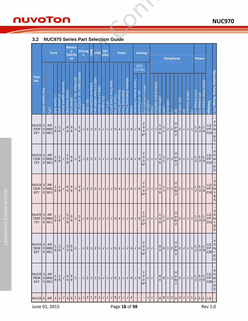
3.2 NUC970 Series Part Selection Guide
Part No.
Core
Memory
Interface
Storage
MA
C
USB Display
Timer Analog
Peripheral Power
Packag
e
Op
era
ting
Tem
p. R
an
ge
(°C )
Max S
peed (M
Hz)
CP
U
I Cache (K
B)
D C
ache (K
B)
Security
again
st p
iracy
DD
R2 R
AM
(MB
)
SR
AM
(KB
)
SP
I Fla
sh, N
o. o
f I/O P
ins
NA
ND
Fla
sh, N
o. o
f EC
C b
its
EM
MC
SD
/ SD
IO
Eth
ern
et 1
0/1
00 M
AC
US
B 2
.0 H
ost (4
80M
bps)
US
B 2
.0 H
S D
evic
e
2D
Gra
phic
s
TF
T L
CD
Real-T
ime C
lock (R
TC
)
Tim
er (3
2-b
it)
Enhanced T
imer
Watc
hdog T
imer
Win
dow
Watc
hdog T
ime
r
PW
M
ADC (12-bit)
LV
D/L
VR
To
uch S
cre
en C
ontro
ller
No. o
f Channels
Speed (S
am
ple
s p
er
second)
JT
AG
Exte
rnal B
us In
terfa
ce
GP
IO (M
ax)
UA
RT
CA
N B
US
I 2C
SP
I
ISO
-7816-3
KP
I
CM
OS
Inte
rface
I²S
Core
Volta
ge (V
)
I/O V
olta
ge (V
)
DD
R2 R
AM
Volta
ge (V
)
NUC972DF62Y
300
ARM926EJ
16
16 √
64
56
1 24 √ 2 2 2 1 √ √ √ 5 4 √ √ 4 √ 8
200K*
√ √ √
146
11
2 2
Up to 2
2 √ √ 1 1.2
3.3
1.8
LQFP216
-40 to +85
NUC972DF72Y
300
ARM926EJ
16
16 √
128
56
1 24 √ 2 2 2 1 √ √ √ 5 4 √ √ 4 √ 8
200K*
√ √ √
146
11
2 2
Up to 2
2 √ √ 1 1.2
3.3
1.8
LQFP216
-40 to +85
NUC973DF62Y
300
ARM926EJ
16
16 √
64
56
1 24 √ 2 2 2 1 √ √ √ 5 4 √ √ 4 √ 5
200K*
√ √ √
148
11
2 2
Up to 2
2 √ √ 1 1.2
3.3
1.8
LQFP216
-40 to +85
NUC973DF72Y
300
ARM926EJ
16
16 √
128
56
1 24 √ 2 2 2 1 √ √ √ 5 4 √ √ 4 √ 5
200K*
√ √ √
148
11
2 2
Up to 2
2 √ √ 1 1.2
3.3
1.8
LQFP216
-40 to +85
NUC976DK52Y
300
ARM926EJ
16
16 √
32
56
1 - √ 2 1 2 1 √ √ √ 5 1 √ √ 4 √ 4
200K*
√ √ - 80
6 1 2
Up to 2
2 √ √ 1 1.2
3.3
1.8
LQFP128
-40 to +85
NUC976DK62Y
300
ARM926EJ
16
16 √
64
56
1 - √ 2 1 2 1 √ √ √ 5 1 √ √ 4 √ 4
200K*
√ √ - 80
6 1 2
Up to 2
2 √ √ 1 1.2
3.3
1.8
LQFP128
-40 to +85
NUC9 3 AR 1 1 √ 3 5 1 2 √ 2 1 2 1 √ √ √ 5 1 √ √ 4 - - - √ √ - 8 8 1 2 U 2 √ √ 1 1. 3. 1. LQ -
NUC970
June 01, 2015 Page 19 of 98 Rev 1.0
NU
C97
0 S
ER
IES
DA
TA
SH
EE
T
77DK52Y
00
M926EJ
6 6 2 6 4 7 p to 2
2 3 8 FP128
40 to +85
NUC977DK62Y
300
ARM926EJ
16
16 √
64
56
1 24 √ 2 1 2 1 √ √ √ 5 1 √ √ 4 - - - √ √ -
87
8 1 2
Up to 2
2 √ √ 1 1.2
3.3
1.8
LQFP128
-40 to +85
NUC970
June 01, 2015 Page 20 of 98 Rev 1.0
NU
C97
0 S
ER
IES
DA
TA
SH
EE
T
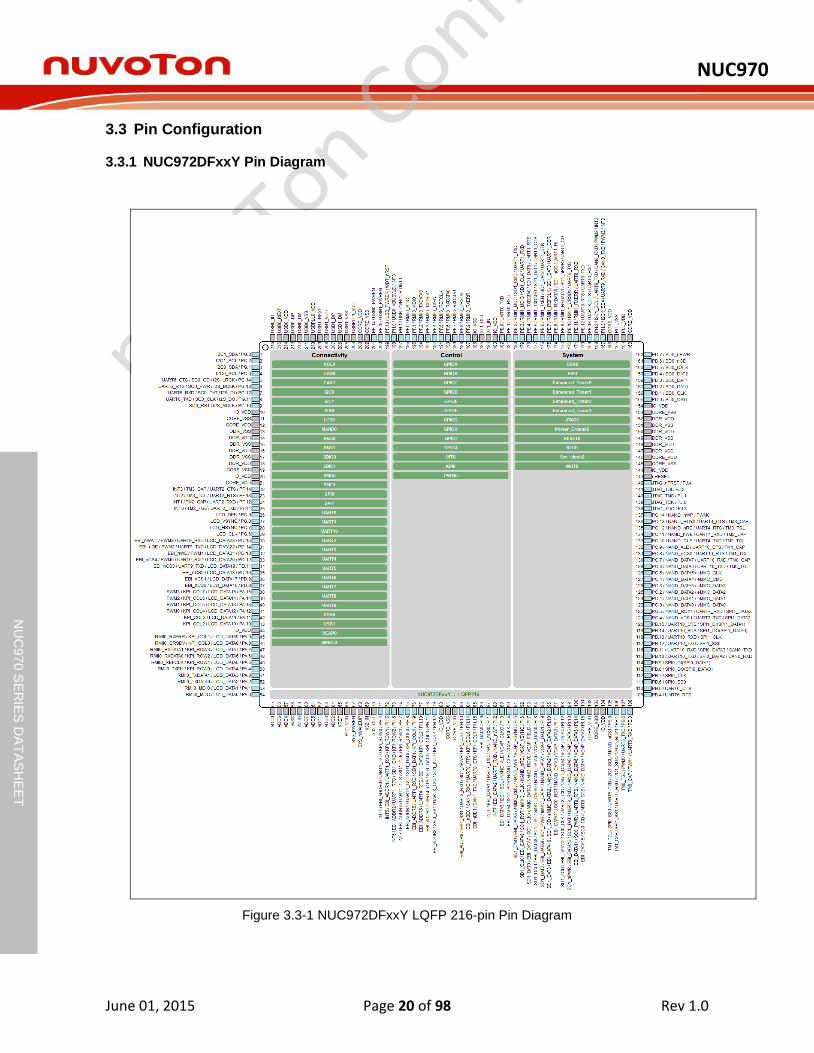
3.3 Pin Configuration
3.3.1 NUC972DFxxY Pin Diagram
Figure 3.3-1 NUC972DFxxY LQFP 216-pin Pin Diagram
NUC970
June 01, 2015 Page 21 of 98 Rev 1.0
NU
C97
0 S
ER
IES
DA
TA
SH
EE
T
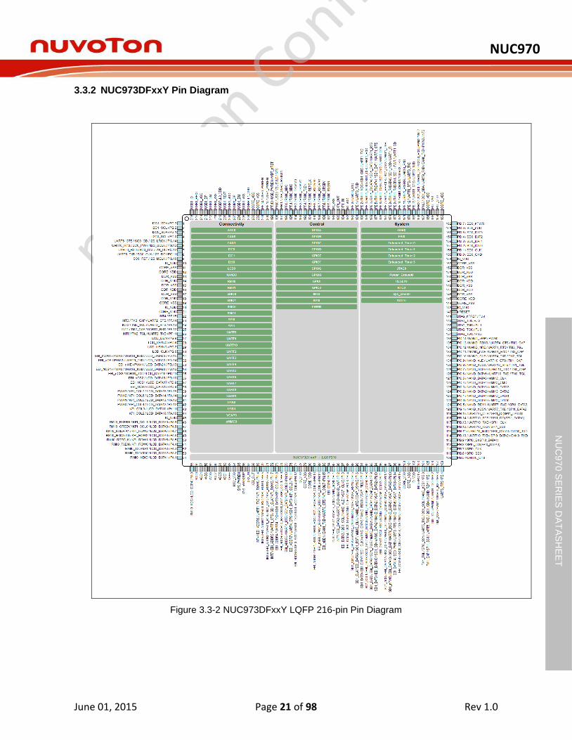
3.3.2 NUC973DFxxY Pin Diagram
Figure 3.3-2 NUC973DFxxY LQFP 216-pin Pin Diagram
NUC970
June 01, 2015 Page 22 of 98 Rev 1.0
NU
C97
0 S
ER
IES
DA
TA
SH
EE
T
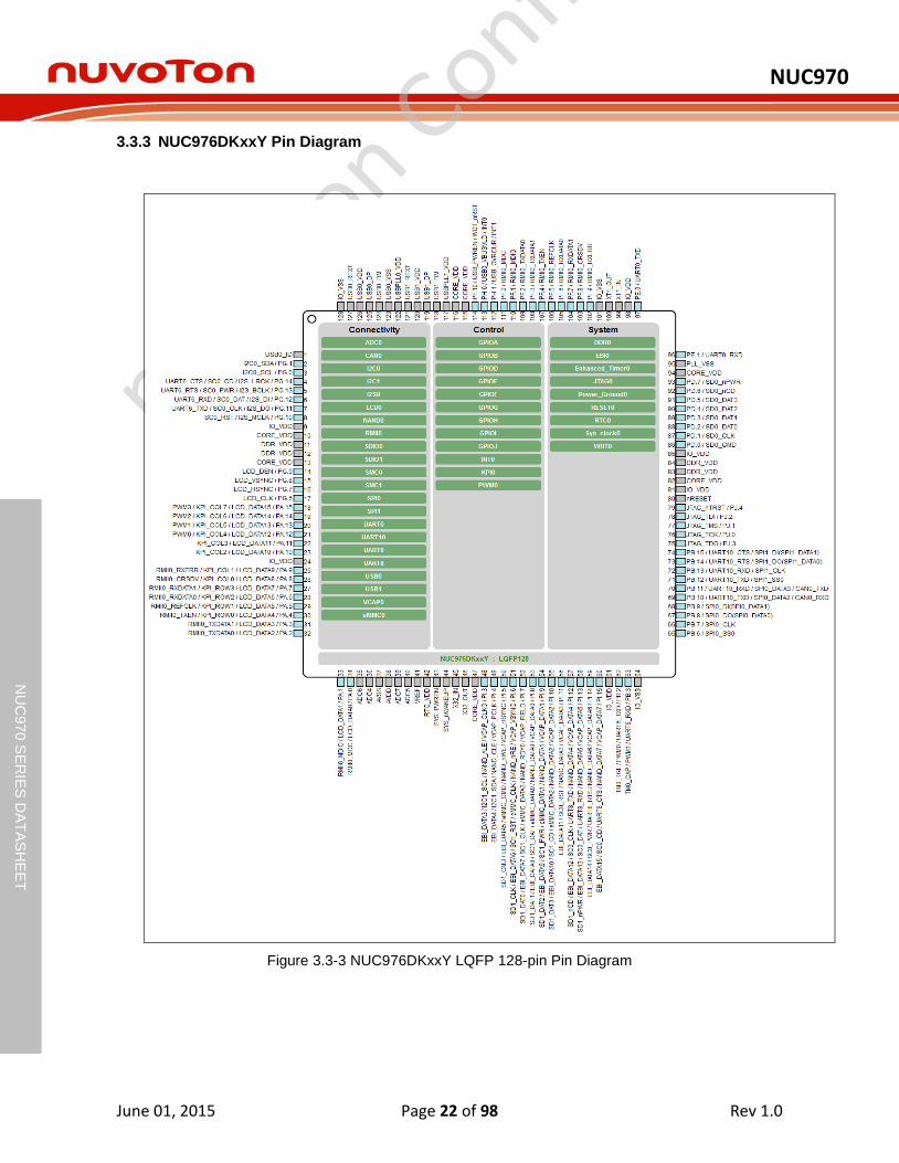
3.3.3 NUC976DKxxY Pin Diagram
Figure 3.3-3 NUC976DKxxY LQFP 128-pin Pin Diagram

NUC970
June 01, 2015 Page 23 of 98 Rev 1.0
NU
C97
0 S
ER
IES
DA
TA
SH
EE
T
3.3.4 NUC977DKxxY Pin Diagram
Figure 3.3-4 NUC977DKxxY LQFP 128-pin Pin Diagram

NUC970
June 01, 2015 Page 24 of 98 Rev 1.0
NU
C97
0 S
ER
IES
DA
TA
SH
EE
T
3.4 Pin Description
NUC972DFxxY
NUC973DFxxY
NUC976DKxxY
NUC977DKxxY
Pin Name Pin Type Description
1 1 - -
PG.3 I/O General purpose digital I/O pin Port G Pin 3.
I2C1_SDA I/O I2C1 data input/output pin.
2 2 - -
PG.2 I/O General purpose digital I/O pin Port G Pin 2.
I2C1_SCL O I2C1 clock pin.
3 3 2 2
PG.1 I/O General purpose digital I/O pin Port G Pin 1.
I2C0_SDA I/O I2C0 data input/output pin.
4 4 3 3
PG.0 I/O General purpose digital I/O pin Port G Pin 0.
I2C0_SCL O I2C0 clock pin.
5 5 4 4
PG.14 I/O General purpose digital I/O pin Port G Pin 14.
I2S_LRCK O I2S left right channel clock.
UART6_CTS I Clear to send input pin for UART6.
SC0_CD I SmartCard0 card detect pin.
CLK_OUT O Reference Clock Output.
6 6 5 5
PG.13 I/O General purpose digital I/O pin Port G Pin 13.
I2S_BCLK I I2S bit clock pin.
UART6_RTS O Request to send output pin for UART6.
SC0_PWR O SmartCard0 power pin.
7 7 6 6
PG.12 I/O General purpose digital I/O pin Port G Pin 12.
I2S_DI I I2S data input.
UART6_RXD I Data receiver input pin for UART6.
SC0_DAT I/O SmartCard0 data pin.
8 8 7 7
PG.11 I/O General purpose digital I/O pin Port G Pin 11.
I2S_DO O I2S data output.
UART6_TXD O Data transmitter output pin for UART6.
NUC970
June 01, 2015 Page 25 of 98 Rev 1.0
NU
C97
0 S
ER
IES
DA
TA
SH
EE
T
NUC972DFxxY
NUC973DFxxY
NUC976DKxxY
NUC977DKxxY
Pin Name Pin Type Description
SC0_CLK O SmartCard0 clock pin.
9 9 8 8
PG.10 I/O General purpose digital I/O pin Port G Pin 10.
I2S_MCLK O I2S master clock output pin.
SC0_RST O SmartCard0 reset pin.
10 10 9 9 IO_VDD P MCU I/O power pin.
11 11 - - CORE_VSS P MCU internal core ground pin.
12 12 10 10 CORE_VDD P MCU internal core power pin.
13 13 - - DDR_VSS P DDR ground pin.
14 14 11 11 DDR_VDD P DDR power pin.
15 15 - - DDR_VSS P DDR ground pin.
16 16 11 11 DDR_VDD P DDR power pin.
17 17 - - DDR_VSS P DDR ground pin.
18 18 12 12 DDR_VDD P DDR power pin.
19 19 - - CORE_VSS P MCU internal core ground pin.
20 20 - - IO_VDD P MCU I/O power pin.
21 21 13 13 CORE_VDD P MCU internal core power pin.
- 22 - -
PF.15 I/O General purpose digital I/O pin Port F Pin 15.
INT4 I External interrupt 4 input pin.
22 23 - -
PF.14 I/O General purpose digital I/O pin Port F Pin 14.
UART2_CTS I Clear to send input pin for UART2.
TM3_CAP I Enhanced TIMER capture input pin.
INT3 I External interrupt 3 input pin.
23 24 - -
PF.13 I/O General purpose digital I/O pin Port F Pin 13.
UART2_RTS O Request to send output pin for UART2.
TM3_TGL O Enhanced TIMER toggle output pin.

NUC970
June 01, 2015 Page 26 of 98 Rev 1.0
NU
C97
0 S
ER
IES
DA
TA
SH
EE
T
NUC972DFxxY
NUC973DFxxY
NUC976DKxxY
NUC977DKxxY
Pin Name Pin Type Description
INT2 I External interrupt 2 input pin.
24 25 - -
PF.12 I/O General purpose digital I/O pin Port F Pin 12.
UART2_RXD I Data receiver input pin for UART2.
TM2_CAP I Enhanced TIMER capture input pin.
INT1 I External interrupt 1 input pin.
25 26 - -
PF.11 I/O General purpose digital I/O pin Port F Pin 11.
UART2_TXD O Data transmitter output pin for UART2.
TM2_TGL O Enhanced TIMER toggle output pin.
INT0 I External interrupt 0 input pin.
26 27 14 14
PG.9 I/O General purpose digital I/O pin Port G Pin 9.
LCD_DEN O Data enable or display control signal.
27 28 15 15
PG.8 I/O General purpose digital I/O pin Port G Pin 8.
LCD_VSYNC O Vertical sync or frame sync.
28 29 16 16
PG.7 I/O General purpose digital I/O pin Port G Pin 7.
LCD_HSYNC O Horizontal sync or line sync.
29 30 17 17
PG.6 I/O General purpose digital I/O pin Port G Pin 6.
LCD_CLK O Pixel clock output.
30 31 - -
PD.15 I/O General purpose digital I/O pin Port D Pin 15.
LCD_DATA23 O LCD pixel data output bit 23.
UART9_RXD I Data receiver input pin for UART9.
PWM3 O PWM3 output pin.
EBI_nWAIT I External I/O wait control.
31 32 - -
PD.14 I/O General purpose digital I/O pin Port D Pin 14.
LCD_DATA22 O LCD pixel data output bit 22.
UART9_TXD O Data transmitter output pin for UART9.
NUC970
June 01, 2015 Page 27 of 98 Rev 1.0
NU
C97
0 S
ER
IES
DA
TA
SH
EE
T
NUC972DFxxY
NUC973DFxxY
NUC976DKxxY
NUC977DKxxY
Pin Name Pin Type Description
PWM2 O PWM2 output pin.
EBI_nOE O External I/O output enable.
32 33 - -
PD.13 I/O General purpose digital I/O pin Port D Pin 13.
LCD_DATA21 O LCD pixel data output bit 21.
PWM1 O PWM1 output pin.
EBI_nWE O External I/O chip write enable.
33 34 - -
PD.12 I/O General purpose digital I/O pin Port D Pin 12.
LCD_DATA20 O LCD pixel data output bit 20.
UART9_RXD I Data receiver input pin for UART9.
PWM0 O PWM0 output pin.
EBI_nCS4 O External I/O chip select bank 4.
34 35 - -
PD.11 I/O General purpose digital I/O pin Port D Pin 11.
LCD_DATA19 O LCD pixel data output bit 19.
UART9_TXD O Data transmitter output pin for UART9.
EBI_nCS3 O External I/O chip select bank 3.
35 36 - -
PD.10 I/O General purpose digital I/O pin Port D Pin 10.
LCD_DATA18 O LCD pixel data output bit 18.
EBI_nCS2 O External I/O chip select bank 2.
36 37 - -
PD.9 I/O General purpose digital I/O pin Port D Pin 9.
LCD_DATA17 O LCD pixel data output bit 17.
EBI_nCS1 O External I/O chip select bank 1.
37 38 - -
PD.8 I/O General purpose digital I/O pin Port D Pin 8.
LCD_DATA16 O LCD pixel data output bit 16.
EBI_nCS0 O External I/O chip select bank 0.
38 39 18 18 PA.15 I/O General purpose digital I/O pin Port A Pin 15.

NUC970
June 01, 2015 Page 28 of 98 Rev 1.0
NU
C97
0 S
ER
IES
DA
TA
SH
EE
T
NUC972DFxxY
NUC973DFxxY
NUC976DKxxY
NUC977DKxxY
Pin Name Pin Type Description
LCD_DATA15 O LCD pixel data output bit 15.
KPI_COL7 I Keypad Column Scan Input Bus 7.
PWM3 O PWM3 output pin.
39 40 19 19
PA.14 I/O General purpose digital I/O pin Port A Pin 14.
LCD_DATA14 O LCD pixel data output bit 14.
KPI_COL6 I Keypad Column Scan Input Bus 6.
PWM2 O PWM2 output pin.
40 41 20 20
PA.13 I/O General purpose digital I/O pin Port A Pin 13.
LCD_DATA13 O LCD pixel data output bit 13.
KPI_COL5 I Keypad Column Scan Input Bus 5.
PWM1 O PWM1 output pin.
41 42 21 21
PA.12 I/O General purpose digital I/O pin Port A Pin 12.
LCD_DATA12 O LCD pixel data output bit 12.
KPI_COL4 I Keypad Column Scan Input Bus 4.
PWM0 O PWM0 output pin.
42 43 22 22
PA.11 I/O General purpose digital I/O pin Port A Pin 11.
LCD_DATA11 O LCD pixel data output bit 11.
KPI_COL3 I Keypad Column Scan Input Bus 3.
43 44 23 23
PA.10 I/O General purpose digital I/O pin Port A Pin 10.
LCD_DATA10 O LCD pixel data output bit 10.
KPI_COL2 I Keypad Column Scan Input Bus 2.
44 45 24 24 IO_VDD P MCU I/O power pin.
45 46 25 25
PA.9 I/O General purpose digital I/O pin Port A Pin 9.
RMII0_RXERR I RMII0 receive data error.
LCD_DATA9 O LCD pixel data output bit 9.

NUC970
June 01, 2015 Page 29 of 98 Rev 1.0
NU
C97
0 S
ER
IES
DA
TA
SH
EE
T
NUC972DFxxY
NUC973DFxxY
NUC976DKxxY
NUC977DKxxY
Pin Name Pin Type Description
KPI_COL1 I Keypad Column Scan Input Bus 1.
PWRON_SET9 I Power On Setting bit 9.
46 47 26 26
PA.8 I/O General purpose digital I/O pin Port A Pin 8.
RMII0_CRSDV I RMII0 carrier sense / receive data valid.
LCD_DATA8 O LCD pixel data output bit 8.
KPI_COL0 I Keypad Column Scan Input Bus 0.
PWRON_SET8 I Power On Setting bit 8.
47 48 27 27
PA.7 I/O General purpose digital I/O pin Port A Pin 7.
RMII0_RXDATA1 I RMII0 receive data bus bit 1.
LCD_DATA7 O LCD pixel data output bit 7.
KPI_ROW3 O Keypad Row Scan Output Bus 3.
PWRON_SET7 I Power On Setting bit 7.
48 49 28 28
PA.6 I/O General purpose digital I/O pin Port A Pin 6.
RMII0_RXDATA0 I RMII0 receive data bus bit 0.
LCD_DATA6 O LCD pixel data output bit 6.
KPI_ROW2 O Keypad Row Scan Output Bus 2.
PWRON_SET6 I Power On Setting bit 6.
49 50 29 29
PA.5 I/O General purpose digital I/O pin Port A Pin 5.
RMII0_REFCLK I RMII0 reference clock.
LCD_DATA5 O LCD pixel data output bit 5.
KPI_ROW1 O Keypad Row Scan Output Bus 1.
PWRON_SET5 I Power On Setting bit 5.
50 51 30 30
PA.4 I/O General purpose digital I/O pin Port A Pin 4.
RMII0_TXEN O RMII0 transmit enable.
LCD_DATA4 O LCD pixel data output bit 4.

NUC970
June 01, 2015 Page 30 of 98 Rev 1.0
NU
C97
0 S
ER
IES
DA
TA
SH
EE
T
NUC972DFxxY
NUC973DFxxY
NUC976DKxxY
NUC977DKxxY
Pin Name Pin Type Description
KPI_ROW0 O Keypad Row Scan Output Bus 0.
PWRON_SET4 I Power On Setting bit 4.
51 52 31 31
PA.3 I/O General purpose digital I/O pin Port A Pin 3.
RMII0_TXDATA1 O RMII0 transmit data bus bit 1.
LCD_DATA3 O LCD pixel data output bit 3.
PWRON_SET3 Power On Setting bit 3.
52 53 32 32
PA.2 I/O General purpose digital I/O pin Port A Pin 2.
RMII0_TXDATA0 O RMII0 Transmit Data bus bit 0.
LCD_DATA2 O LCD pixel data output bit 2.
PWRON_SET2 Power On Setting bit 2.
53 54 33 33
PA.1 I/O General purpose digital I/O pin Port A Pin 1.
RMII0_MDIO I/O RMII0 Management Data I/O
LCD_DATA1 O LCD pixel data output bit 1.
PWRON_SET1 Power On Setting bit 1.
54 55 34 34
PA.0 I/O General purpose digital I/O pin Port A Pin 0.
RMII0_MDC O RMII0 Management Data Clock
LCD_DATA0 O LCD pixel data output bit 0.
PWRON_SET0 Power On Setting bit 0.
55 - - - ADC0 I ADC input channel 0 or VBAT.
56 56 35 - ADC6 I ADC input channel 6 or XM.
57 57 36 - ADC4 I ADC input channel 4 or YM.
58 58 37 - AVSS P Ground pin for analog circuit.
59 59 38 - AVDD P Power supply for internal analog circuit.
60 60 39 - ADC7 I ADC input channel 7 or XP.
61 61 40 - ADC5 I ADC input channel 5 or YP.

NUC970
June 01, 2015 Page 31 of 98 Rev 1.0
NU
C97
0 S
ER
IES
DA
TA
SH
EE
T
NUC972DFxxY
NUC973DFxxY
NUC976DKxxY
NUC977DKxxY
Pin Name Pin Type Description
62 62 - - ADC1 I ADC input channel 1.
63 - - - ADC3 I ADC input channel 3 or VSENSE.
64 - - - ADC2 I ADC input channel 2.
65 63 41 - VREF I ADC voltage reference pin.
66 64 42 35 RTC_VDD P RTC power input.
67 65 43 36 SYS_PWREN O RTC wake-up output pin for external DC/DC
enable pin control.
68 66 44 37 SYS_nWAKEUP I RTC wake-up interrupt input with internal pull-high.
69 67 45 38 X32_IN I External 32.768kHz crystal input.
70 68 46 39 X32_OUT O External 32.768kHz crystal output.
71 69 - -
PH.4 I/O General purpose digital I/O pin Port H Pin 4.
KPI_ROW0 O Keypad Row Scan Output Bus 0.
UART1_TXD O Data transmitter output pin for UART1.
EBI_ADDR0 O External I/O address bus bit 0.
INT4 I External interrupt 4 input pin.
72 70 - -
PH.5 I/O General purpose digital I/O pin Port H Pin 5.
KPI_ROW1 O Keypad Row Scan Output Bus 1.
UART1_RXD I Data receiver input pin for UART1.
EBI_ADDR1 O External I/O address bus bit 1.
INT5 I External interrupt 5 input pin.
73 71 - -
PH.6 I/O General purpose digital I/O pin Port H Pin 6.
KPI_ROW2 O Keypad Row Scan Output Bus 2.
SD1_CMD O SD/SDIO Port 1 – command/response.
UART1_RTS O Request to send output pin for UART1.
EBI_ADDR2 O External I/O address bus bit 2.
INT6 I External interrupt 6 input pin.

NUC970
June 01, 2015 Page 32 of 98 Rev 1.0
NU
C97
0 S
ER
IES
DA
TA
SH
EE
T
NUC972DFxxY
NUC973DFxxY
NUC976DKxxY
NUC977DKxxY
Pin Name Pin Type Description
74 72 - 40
PH.7 I/O General purpose digital I/O pin Port H Pin 7.
KPI_ROW3 O Keypad Row Scan Output Bus 3.
SD1_CLK O SD/SDIO Port 1 – clock.
UART1_CTS I Clear to send input pin for UART1.
EBI_ADDR3 O External I/O address bus bit 3.
INT7 I External interrupt 7 input pin.
75 73 - -
PH.8 I/O General purpose digital I/O pin Port H Pin 8.
KPI_COL0 I Keypad Column Scan Input Bus 0.
SD1_DAT0 I/O SD/SDIO mode #1 data line bit 0.
UART4_TXD O Data transmitter output pin for UART4.
EBI_ADDR4 O External I/O address bus bit 4.
76 74 - -
PH.9 I/O General purpose digital I/O pin Port H Pin 9.
KPI_COL1 I Keypad Column Scan Input Bus 1.
SD1_DAT1 I/O SD/SDIO mode #1 data line bit 1.
UART4_RXD I Data receiver input pin for UART4.
EBI_ADDR5 O External I/O address bus bit 5.
77 75 - -
PH.10 I/O General purpose digital I/O pin Port H Pin 10.
KPI_COL2 I Keypad Column Scan Input Bus 2.
SD1_DAT2 I/O SD/SDIO mode #1 data line bit 2.
UART4_RTS O Request to send output pin for UART4.
EBI_ADDR6 O External I/O address bus bit 6.
78 76 - -
PH.11 I/O General purpose digital I/O pin Port H Pin 11.
KPI_COL3 I Keypad Column Scan Input Bus 3.
SD1_DAT3 I/O SD/SDIO mode #1 data line bit 3.
UART4_CTS I Clear to send input pin for UART4.

NUC970
June 01, 2015 Page 33 of 98 Rev 1.0
NU
C97
0 S
ER
IES
DA
TA
SH
EE
T
NUC972DFxxY
NUC973DFxxY
NUC976DKxxY
NUC977DKxxY
Pin Name Pin Type Description
EBI_ADDR7 O External I/O address bus bit 7.
79 77 - -
PH.12 I/O General purpose digital I/O pin Port H Pin 12.
KPI_COL4 I Keypad Column Scan Input Bus 4.
SD1_nCD I SD/SDIO mode #1 – card detect.
UART8_TXD O Data transmitter output pin for UART8.
SPI0_SS1 2nd SPI0 chip select pin.
EBI_ADDR8 O External I/O address bus bit 8.
80 78 - - IO_VDD P MCU I/O power pin.
81 79 - - CORE_VSS P MCU internal core ground pin.
82 80 47 41 CORE_VDD P MCU internal core power pin.
83 81 - -
PH.13 I/O General purpose digital I/O pin Port H Pin 13.
KPI_COL5 I Keypad Column Scan Input Bus 5.
SD1_nPWR O SD/SDIO mode #1 – power enable.
UART8_RXD I Data receiver input pin for UART8.
SPI1_SS1 2nd SPI1 chip select pin.
EBI_ADDR9 O External I/O address bus bit 9.
84 82 - -
PH.14 I/O General purpose digital I/O pin Port H Pin 14.
KPI_COL6 I Keypad Column Scan Input Bus 6.
UART8_RTS O Request to send output pin for UART8.
CAN1_RXD I CAN bus receiver1 input.
EBI_nBE0 O External I/O low byte enable.
85 83 - -
PH.15 I/O General purpose digital I/O pin Port H Pin 15.
KPI_COL7 I Keypad Column Scan Input Bus 7.
UART8_CTS I Clear to send input pin for UART8.
CAN1_TXD O CAN bus transmitter1 output.

NUC970
June 01, 2015 Page 34 of 98 Rev 1.0
NU
C97
0 S
ER
IES
DA
TA
SH
EE
T
NUC972DFxxY
NUC973DFxxY
NUC976DKxxY
NUC977DKxxY
Pin Name Pin Type Description
EBI_nBE1 O External I/O high byte enable.
86 84 - -
PI.0 I/O General purpose digital I/O pin Port I Pin 0.
EBI_DATA0 I/O External I/O data bus bit 0.
87 85 - 42
PI.1 I/O General purpose digital I/O pin Port I Pin 1.
NAND_nCS0 O NAND flash chip select 0.
UART7_TXD O Data transmitter output pin for UART7.
EBI_DATA1 I/O External I/O data bus bit 1.
INT6 I External interrupt 6 input pin.
88 86 - 43
PI.2 I/O General purpose digital I/O pin Port I Pin 2.
NAND_nWP O NAND flash srite protect.
UART7_RXD I Data receiver input pin for UART7.
EBI_DATA2 I/O External I/O data bus bit 2.
INT7 I External interrupt 7 input pin.
89 87 48 44
PI.3 I/O General purpose digital I/O pin Port I Pin 3.
VCAP_CLKO O Sensor interface system clock.
NAND_ALE O NAND flash address latch enable.
I2C1_SCL O I2C1 clock pin.
EBI_DATA3 I/O External I/O data bus bit 3.
90 88 49 45
PI.4 I/O General purpose digital I/O pin Port I Pin 4.
VCAP_PCLK I Sensor interface pixel clock.
NAND_CLE O NAND flash command latch enable.
I2C1_SDA I/O I2C1 data input/output pin.
EBI_DATA4 I/O External I/O data bus bit 4.
91 89 50 46
PI.5 I/O General purpose digital I/O pin Port I Pin 5.
VCAP_HSYNC I Sensor interface HSYNC.

NUC970
June 01, 2015 Page 35 of 98 Rev 1.0
NU
C97
0 S
ER
IES
DA
TA
SH
EE
T
NUC972DFxxY
NUC973DFxxY
NUC976DKxxY
NUC977DKxxY
Pin Name Pin Type Description
NAND_nWE O NAND flash write enable.
eMMC_CMD I/O eMMC command/Response.
EBI_DATA5 I/O External I/O data bus bit 5.
92 90 51 47
PI.6 I/O General purpose digital I/O pin Port I Pin 6.
VCAP_VSYNC I Sensor interface VSYNC.
NAND_nRE O NAND flash read enable.
eMMC_CLK O eMMC clock output.
SC1_RST O SmartCard1 reset pin.
EBI_DATA6 I/O External I/O data bus bit 6.
93 91 52 48
PI.7 I/O General purpose digital I/O pin Port I Pin 7.
VCAP_FIELD I Sensor interface even/odd field indicator.
NAND_RDY0 I NAND flash ready/busy channel 0.
eMMC_DATA3 I/O eMMC data line bit 3.
SC1_CLK O SmartCard1 clock pin.
EBI_DATA7 I/O External I/O data bus bit 7.
94 92 53 49
PI.8 I/O General purpose digital I/O pin Port I Pin 8.
VCAP_DATA0 I Sensor interface data bus bit 0.
NAND_DATA0 I/O NAND flash data bus bit 0.
eMMC_DATA0 I/O eMMC data line bit 0.
SC1_DAT I/O SmartCard1 data pin.
EBI_DATA8 I/O External I/O data bus bit 8.
95 93 54 50
PI.9 I/O General purpose digital I/O pin Port I Pin 9.
VCAP_DATA1 I Sensor interface data bus bit 1.
NAND_DATA1 I/O NAND flash data bus bit 1.
eMMC_DATA1 I/O eMMC data line bit 1.

NUC970
June 01, 2015 Page 36 of 98 Rev 1.0
NU
C97
0 S
ER
IES
DA
TA
SH
EE
T
NUC972DFxxY
NUC973DFxxY
NUC976DKxxY
NUC977DKxxY
Pin Name Pin Type Description
SC1_PWR O SmartCard1 power pin.
EBI_DATA9 I/O External I/O data bus bit 9.
96 94 55 51
PI.10 I/O General purpose digital I/O pin Port I Pin 10.
VCAP_DATA2 I Sensor interface data bus bit 2.
NAND_DATA2 I/O NAND flash data bus bit 2.
eMMC_DATA2 I/O eMMC data line bit 2.
SC1_CD I SmartCard1 card detect pin.
EBI_DATA10 I/O External I/O data bus bit 10.
97 95 56 52
PI.11 I/O General purpose digital I/O pin Port I Pin 11.
VCAP_DATA3 I Sensor interface data bus bit 3.
NAND_DATA3 I/O NAND flash data bus bit 3.
SC0_RST O SmartCard0 reset pin.
EBI_DATA11 I/O External I/O data bus bit 11.
98 96 57 53
PI.12 I/O General purpose digital I/O pin Port I Pin 12.
VCAP_DATA4 I Sensor interface data bus bit 4.
NAND_DATA4 I/O NAND flash data bus bit 4.
UART8_TXD O Data transmitter output pin for UART8.
SC0_CLK O SmartCard0 clock pin.
EBI_DATA12 I/O External I/O data bus bit 12.
99 97 58 54
PI.13 I/O General purpose digital I/O pin Port I Pin 13.
VCAP_DATA5 I Sensor interface data bus bit 5.
NAND_DATA5 I/O NAND flash data bus bit 5.
UART8_RXD I Data receiver input pin for UART8.
SC0_DAT I/O SmartCard0 data pin.
EBI_DATA13 I/O External I/O data bus bit 13.
NUC970
June 01, 2015 Page 37 of 98 Rev 1.0
NU
C97
0 S
ER
IES
DA
TA
SH
EE
T
NUC972DFxxY
NUC973DFxxY
NUC976DKxxY
NUC977DKxxY
Pin Name Pin Type Description
100 98 59 55
PI.14 I/O General purpose digital I/O pin Port I Pin 14.
VCAP_DATA6 I Sensor interface data bus bit 6.
NAND_DATA6 I/O NAND flash data bus bit 6.
UART8_RTS O Request to send output pin for UART8.
SC0_PWR O SmartCard0 power pin.
EBI_DATA14 I/O External I/O data bus bit 14.
101 99 60 56
PI.15 I/O General purpose digital I/O pin Port I Pin 15.
VCAP_DATA7 I Sensor interface data bus bit 7.
NAND_DATA7 I/O NAND flash data bus bit 7.
UART8_CTS I Clear to send input pin for UART8.
SC0_CD I SmartCard0 card detect pin.
EBI_DATA15 I/O External I/O data bus bit 15.
102 100 - - CORE_VDD P MCU internal core power pin.
103 101 - - CORE_VSS P MCU internal core ground pin.
104 102 61 57 IO_VDD P MCU I/O power pin.
- 103 - -
PG.15 I/O General purpose digital I/O pin Port G Pin 15.
INT5 I External interrupt 5 input pin.
105 104 - 58
PB.0 I/O General purpose digital I/O pin Port B Pin 0.
NAND_nCS1 O NAND flash chip select 1.
UART5_TXD O Data transmitter output pin for UART5.
SPI0_SS1 2nd SPI0 chip select pin.
TM1_TGL O Enhanced TIMER toggle output pin.
106 105 - 59
PB.1 I/O General purpose digital I/O pin Port B Pin 1.
NAND_RDY1 I NAND flash ready/busy channel 1.
UART5_RXD I Data receiver input pin for UART5.

NUC970
June 01, 2015 Page 38 of 98 Rev 1.0
NU
C97
0 S
ER
IES
DA
TA
SH
EE
T
NUC972DFxxY
NUC973DFxxY
NUC976DKxxY
NUC977DKxxY
Pin Name Pin Type Description
SPI1_SS1 2nd SPI1 chip select pin.
TM1_CAP I Enhanced TIMER capture input pin.
107 106 62 60
PB.2 I/O General purpose digital I/O pin Port B Pin 2.
UART6_TXD O Data transmitter output pin for UART6.
PWM0 O PWM0 output pin.
TM0_TGL O Enhanced TIMER toggle output pin.
108 107 63 61
PB.3 I/O General purpose digital I/O pin Port B Pin 3.
UART6_RXD I Data receiver input pin for UART6.
PWM1 O PWM1 output pin.
TM0_CAP I Enhanced TIMER capture input pin.
109 108 - 62
PB.4 I/O General purpose digital I/O pin Port B Pin 4.
UART6_RTS O Request to send output pin for UART6.
110 109 - 63
PB.5 I/O General purpose digital I/O pin Port B Pin 5.
UART6_CTS I Clear to send input pin for UART6.
- - 64 64 IO_VSS P MCU I/O ground pin.
111 110 65 65
PB.6 I/O General purpose digital I/O pin Port B Pin 6.
SPI0_SS0 1st SPI0 chip select pin.
112 111 66 66
PB.7 I/O General purpose digital I/O pin Port B Pin 7.
SPI0_CLK SPI0 serial clock pin.
113 112 67 67
PB.8 I/O General purpose digital I/O pin Port B Pin 8.
SPI0_DO
(SPI0_DATA0)
SPI0 Data out pin. SPI0 data 0 in dual/quad mode.
114 113 68 68
PB.9 I/O General purpose digital I/O pin Port B Pin 9.
SPI0_DI
(SPI0_DATA1)
SPI0 Data input pin. SPI0 data 1 in dual/quad mode.
115 114 69 69 PB.10 I/O General purpose digital I/O pin Port B Pin 10.

NUC970
June 01, 2015 Page 39 of 98 Rev 1.0
NU
C97
0 S
ER
IES
DA
TA
SH
EE
T
NUC972DFxxY
NUC973DFxxY
NUC976DKxxY
NUC977DKxxY
Pin Name Pin Type Description
UART10_TXD O Data transmitter output pin for UART10.
SPI0_DATA2 SPI0 data 2 in dual/quad mode.
CAN0_RXD I CAN bus receiver0 input.
116 115 70 70
PB.11 I/O General purpose digital I/O pin Port B Pin 11.
UART10_RXD I Data receiver input pin for UART10.
SPI0_DATA3 SPI0 data 3 in dual/quad mode.
CAN0_TXD O CAN bus transmitter0 output.
117 116 71 71
PB.12 I/O General purpose digital I/O pin Port B Pin 12.
UART10_TXD O Data transmitter output pin for UART10.
SPI1_SS0 1st SPI1 chip select pin.
118 117 72 72
PB.13 I/O General purpose digital I/O pin Port B Pin 13.
UART10_RXD I Data receiver input pin for UART10.
SPI1_CLK SPI1 serial clock pin.
119 118 73 73
PB.14 I/O General purpose digital I/O pin Port B Pin 14.
UART10_RTS O Request to send output pin for UART10.
SPI1_DO
(SPI1_DATA0)
SPI1 Data out pin. SPI1 data 0 in dual/quad mode.
120 1119 74 74
PB.15 I/O General purpose digital I/O pin Port B Pin 15.
UART10_CTS I Clear to send input pin for UART10.
SPI1_DI
(SPI1_DATA1)
SPI1 Data input pin. SPI1 data 1 in dual/quad mode.
121 120 - -
PG.4 I/O General purpose digital I/O pin Port G Pin 4.
NAND_nCS1 O NAND flash chip select 1.
UART7_TXD O Data transmitter output pin for UART7.
SPI1_DATA2 SPI1 data 2 in dual/quad mode.
122 121 - - PG.5 I/O General purpose digital I/O pin Port G Pin 5.

NUC970
June 01, 2015 Page 40 of 98 Rev 1.0
NU
C97
0 S
ER
IES
DA
TA
SH
EE
T
NUC972DFxxY
NUC973DFxxY
NUC976DKxxY
NUC977DKxxY
Pin Name Pin Type Description
NAND_RDY1 I NAND flash ready/busy channel 1.
UART7_RXD I Data receiver input pin for UART7.
SPI1_DATA3 SPI1 data 3 in dual/quad mode.
123 122 - -
PC.0 I/O General purpose digital I/O pin Port C Pin 0.
NAND_DATA0 I/O NAND flash data bus bit 0.
eMMC_DATA0 I/O eMMC data line bit 0.
124 123 - -
PC.1 I/O General purpose digital I/O pin Port C Pin 1.
NAND_DATA1 I/O NAND flash data bus bit 1.
eMMC_DATA1 I/O eMMC data line bit 1.
125 124 - -
PC.2 I/O General purpose digital I/O pin Port C Pin 2.
NAND_DATA2 I/O NAND flash data bus bit 2.
eMMC_DATA2 I/O eMMC data line bit 2.
126 125 - -
PC.3 I/O General purpose digital I/O pin Port C Pin 3.
NAND_DATA3 I/O NAND flash data bus bit 3.
eMMC_DATA3 I/O eMMC data line bit 3.
127 126 - -
PC.4 I/O General purpose digital I/O pin Port C Pin 4.
NAND_DATA4 I/O NAND flash data bus bit 4.
eMMC_CMD I/O eMMC command/Response.
128 127 - -
PC.5 I/O General purpose digital I/O pin Port C Pin 5.
NAND_DATA5 I/O NAND flash data bus bit 5.
eMMC_CLK O eMMC clock output.
129 128 - -
PC.6 I/O General purpose digital I/O pin Port C Pin 6.
NAND_DATA6 I/O NAND flash data bus bit 6.
UART10_TXD O Data transmitter output pin for UART10.
TM0_TGL O Enhanced TIMER toggle output pin.

NUC970
June 01, 2015 Page 41 of 98 Rev 1.0
NU
C97
0 S
ER
IES
DA
TA
SH
EE
T
NUC972DFxxY
NUC973DFxxY
NUC976DKxxY
NUC977DKxxY
Pin Name Pin Type Description
130 129 - -
PC.7 I/O General purpose digital I/O pin Port C Pin 7.
NAND_DATA7 I/O NAND flash data bus bit 7.
UART10_RXD I Data receiver input pin for UART10.
TM0_CAP I Enhanced TIMER capture input pin.
131 130 - -
PC.8 I/O General purpose digital I/O pin Port C Pin 8.
NAND_nCS0 O NAND flash chip select 0.
UART10_RTS O Request to send output pin for UART10.
TM1_TGL O Enhanced TIMER toggle output pin.
132 131 - -
PC.9 I/O General purpose digital I/O pin Port C Pin 9.
NAND_ALE O NAND flash address latch enable.
UART10_CTS I Clear to send input pin for UART10.
TM1_CAP I Enhanced TIMER capture input pin.
133 132 - -
PC.10 I/O General purpose digital I/O pin Port C Pin 10.
NAND_CLE O NAND flash command latch enable.
UART4_TXD O Data transmitter output pin for UART4.
TM2_TGL O Enhanced TIMER toggle output pin.
134 133 - -
PC.11 I/O General purpose digital I/O pin Port C Pin 11.
NAND_nWE O NAND flash write enable.
UART4_RXD I Data receiver input pin for UART4.
TM2_CAP I Enhanced TIMER capture input pin.
135 134 - -
PC.12 I/O General purpose digital I/O pin Port C Pin 12.
NAND_nRE O NAND flash read enable.
UART4_RTS O Request to send output pin for UART4.
TM3_TGL O Enhanced TIMER toggle output pin.
136 135 - - PC.13 I/O General purpose digital I/O pin Port C Pin 13.

NUC970
June 01, 2015 Page 42 of 98 Rev 1.0
NU
C97
0 S
ER
IES
DA
TA
SH
EE
T
NUC972DFxxY
NUC973DFxxY
NUC976DKxxY
NUC977DKxxY
Pin Name Pin Type Description
NAND_RDY0 I NAND flash ready/busy channel 0.
UART4_CTS I Clear to send input pin for UART4.
TM3_CAP I Enhanced TIMER capture input pin.
137 136 - -
PC.14 I/O General purpose digital I/O pin Port C Pin 14.
NAND_nWP O NAND flash write protect.
PWM0 O PWM0 output pin.
138 137 75 75
PJ.3 I/O General purpose digital I/O pin Port J Pin 3.
JTAG_TDO O JTAG test data out.
139 138 76 76
PJ.0 I/O General purpose digital I/O pin Port J Pin 0.
JTAG_TCK O JTAG test clock.
140 139 77 77
PJ.1 I/O General purpose digital I/O pin Port J Pin 1.
JTAG_TMS O JTAG test mode select.
141 140 78 78
PJ.2 I/O General purpose digital I/O pin Port J Pin 2.
JTAG_TDI I JTAG test data in.
142 141 79 79
PJ.4 I/O General purpose digital I/O pin Port J Pin 4.
JTAG_nTRST O JTAG Reset.
143 142 80 80 nRESET I External reset input: active LOW, with an internal
pull-up. Set this pin low reset to initial state.
144 143 81 81 IO_VDD P MCU I/O power pin.
145 144 - - CORE_VSS P MCU internal core ground pin.
146 145 82 82 CORE_VDD P MCU internal core power pin.
147 146 - - DDR_VSS P DDR ground pin.
148 147 83 83 DDR_VDD P DDR power pin.
149 148 - - DDR_VSS P DDR ground pin.
150 149 83 83 DDR_VDD P DDR power pin.
151 150 - - DDR_VSS P DDR ground pin.

NUC970
June 01, 2015 Page 43 of 98 Rev 1.0
NU
C97
0 S
ER
IES
DA
TA
SH
EE
T
NUC972DFxxY
NUC973DFxxY
NUC976DKxxY
NUC977DKxxY
Pin Name Pin Type Description
152 151 84 84 DDR_VDD P DDR power pin.
- 152 - - DDR_VSS P DDR ground pin.
153 153 - - CORE_VSS P MCU internal core ground pin.
154 154 85 85 IO_VDD P MCU I/O power pin.
155 155 86 86
PD.0 I/O General purpose digital I/O pin Port D Pin 0.
SD0_CMD O SD/SDIO mode #0 command/response.
156 156 87 87
PD.1 I/O General purpose digital I/O pin Port D Pin 1.
SD0_CLK O SD/SDIO mode #0 clock.
157 157 88 88
PD.2 I/O General purpose digital I/O pin Port D Pin 2.
SD0_DAT0 I/O SD/SDIO mode #0 data line bit 0.
158 158 89 89
PD.3 I/O General purpose digital I/O pin Port D Pin 3.
SD0_DAT1 I/O SD/SDIO mode #0 data line bit 1.
159 159 90 90
PD.4 I/O General purpose digital I/O pin Port D Pin 4.
SD0_DAT2 I/O SD/SDIO mode #0 data line bit 2.
160 160 91 91
PD.5 I/O General purpose digital I/O pin Port D Pin 5.
SD0_DAT3 I/O SD/SDIO mode #0 data line bit 3.
161 161 92 92
PD.6 I/O General purpose digital I/O pin Port D Pin 6.
SD0_nCD I SD/SDIO mode #0 card detect.
162 162 93 93 PD.7 I/O General purpose digital I/O pin Port D Pin 7.
163 163 94 94 CORE_VDD P MCU internal core power pin.
164 164 - - PLL_VDD P PLL power input pin.
165 165 95 95 PLL_VSS P PLL ground.
166 166 - - CORE_VDD P MCU internal core power pin.
167 167 - -
PH.3 I/O General purpose digital I/O pin Port H Pin 3.
I2C1_SDA I/O I2C1 data input/output pin.

NUC970
June 01, 2015 Page 44 of 98 Rev 1.0
NU
C97
0 S
ER
IES
DA
TA
SH
EE
T
NUC972DFxxY
NUC973DFxxY
NUC976DKxxY
NUC977DKxxY
Pin Name Pin Type Description
UART9_RXD I Data receiver input pin for UART9.
CAN0_TXD O CAN bus transmitter0 output.
PWM3 O PWM3 output pin.
INT3 I External interrupt 3 input pin.
168 168 - -
PH.2 I/O General purpose digital I/O pin Port H Pin 2.
I2C1_SCL O I2C1 clock pin.
UART9_TXD O Data transmitter output pin for UART9.
CAN0_RXD I CAN bus receiver0 input.
PWM2 O PWM2 output pin.
INT2 I External interrupt 2 input pin.
169 169 - -
PE.13 I/O General purpose digital I/O pin Port E Pin 13.
UART8_CTS I Clear to send input pin for UART8.
UART3_RXD I Data receiver input pin for UART3.
170 170 - -
PE.12 I/O General purpose digital I/O pin Port E Pin 12.
UART8_RTS O Request to send output pin for UART8.
UART3_TXD O Data transmitter output pin for UART3.
171 171 - -
PE.11 I/O General purpose digital I/O pin Port E Pin 11.
RMII1_RXERR I RMII1 receive data error.
UART8_RXD I Data receiver input pin for UART8.
172 172 - -
PE.10 I/O General purpose digital I/O pin Port E Pin 10.
RMII1_CRSDV I RMII1 carrier sense / receive data valid.
UART8_TXD O Data transmitter output pin for UART8.
173 173 - -
PE.9 I/O General purpose digital I/O pin Port E Pin 9.
RMII1_RXDATA1 I RMII1 receive data bus bit 1.
SD1_nPWR O SD/SDIO mode #1 power enable.

NUC970
June 01, 2015 Page 45 of 98 Rev 1.0
NU
C97
0 S
ER
IES
DA
TA
SH
EE
T
NUC972DFxxY
NUC973DFxxY
NUC976DKxxY
NUC977DKxxY
Pin Name Pin Type Description
UART1_CD I Carrier detect input pin for UART1.
174 174 - -
PE.8 I/O General purpose digital I/O pin Port E Pin 8.
RMII1_RXDATA0 I RMII1 receive data bus bit 0.
SD1_nCD I SD/SDIO mode #1 card detect.
UART1_RI I Ring indicator input pin for UART1.
175 175 - -
PE.7 I/O General purpose digital I/O pin Port E Pin 7.
RMII1_REFCLK I RMII1 reference clock.
SD1_DAT3 I/O SD/SDIO mode #1 data line bit 3.
UART1_DSR I Data set ready input pin for UART1.
176 176 - -
PE.6 I/O General purpose digital I/O pin Port E Pin 6.
RMII1_TXEN O RMII1 transmit enable.
SD1_DAT2 I/O SD/SDIO mode #1 data line bit 2.
UART1_DTR O Data terminal ready output pin for UART1.
177 177 - -
PE.5 I/O General purpose digital I/O pin Port E Pin 5.
RMII1_TXDATA1 O RMII1 transmit data bus bit 1.
SD1_DAT1 I/O SD/SDIO mode #1 data line bit 1.
UART1_CTS I Clear to send input pin for UART1.
178 178 - -
PE.4 I/O General purpose digital I/O pin Port E Pin 4.
RMII1_TXDATA0 O RMII1 Transmit Data bus
SD1_DAT0 I/O SD/SDIO mode #1 ata line bit 0.
UART1_RTS O Request to send output pin for UART1.
179 179 - -
PE.3 I/O General purpose digital I/O pin Port E Pin 3.
RMII1_MDIO I/O RMII1 Management Data I/O
SD1_CLK O SD/SDIO mode #1 clock.
UART1_RXD I Data receiver input pin for UART1.

NUC970
June 01, 2015 Page 46 of 98 Rev 1.0
NU
C97
0 S
ER
IES
DA
TA
SH
EE
T
NUC972DFxxY
NUC973DFxxY
NUC976DKxxY
NUC977DKxxY
Pin Name Pin Type Description
180 180 - -
PE.2 I/O General purpose digital I/O pin Port E Pin 2.
RMII1_MDC O RMII1 Management Data Clock
SD1_CMD O SD/SDIO mode #1 command/response.
UART1_TXD O Data transmitter output pin for UART1.
181 181 96 96
PE.1 I/O General purpose digital I/O pin Port E Pin 1.
UART0_RXD I Data receiver input pin for UART0.
182 182 97 97
PE.0 I/O General purpose digital I/O pin Port E Pin 0.
UART0_TXD O Data transmitter output pin for UART0.
183 183 98 98 IO_VDD P MCU I/O power pin.
184 184 99 99 XT1_IN I External 12MHz crystal input pin.
185 185 100 100 XT1_OUT O External 12MHz crystal output pin.
186 186 101 101 IO_VSS P MCU I/O ground pin.
187 187 102 102
PF.9 I/O General purpose digital I/O pin Port F Pin 9.
RMII0_RXERR I RMII0 receive data error.
188 188 103 103
PF.8 I/O General purpose digital I/O pin Port F Pin 8.
RMII0_CRSDV I RMII0 carrier sense / receive data valid.
189 189 104 104
PF.7 I/O General purpose digital I/O pin Port F Pin 7.
RMII0_RXDATA1 I RMII0 receive data bus bit 1.
190 190 105 105
PF.6 I/O General purpose digital I/O pin Port F Pin 6.
RMII0_RXDATA0 I RMII0 receive data bus bit 0.
191 191 106 106
PF.5 I/O General purpose digital I/O pin Port F Pin 5.
RMII0_REFCLK I RMII0 reference clock.
192 192 107 107
PF.4 I/O General purpose digital I/O pin Port F Pin 4.
RMII0_TXEN O RMII0 transmit enable.
193 193 108 108 PF.3 I/O General purpose digital I/O pin Port F Pin 3.
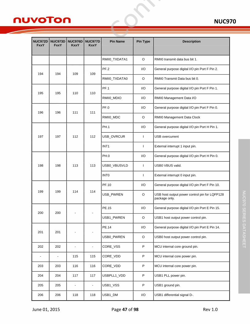
NUC970
June 01, 2015 Page 47 of 98 Rev 1.0
NU
C97
0 S
ER
IES
DA
TA
SH
EE
T
NUC972DFxxY
NUC973DFxxY
NUC976DKxxY
NUC977DKxxY
Pin Name Pin Type Description
RMII0_TXDATA1 O RMII0 transmit data bus bit 1.
194 194 109 109
PF.2 I/O General purpose digital I/O pin Port F Pin 2.
RMII0_TXDATA0 O RMII0 Transmit Data bus bit 0.
195 195 110 110
PF.1 I/O General purpose digital I/O pin Port F Pin 1.
RMII0_MDIO I/O RMII0 Management Data I/O
196 196 111 111
PF.0 I/O General purpose digital I/O pin Port F Pin 0.
RMII0_MDC O RMII0 Management Data Clock
197 197 112 112
PH.1 I/O General purpose digital I/O pin Port H Pin 1.
USB_OVRCUR I USB overcurrent
INT1 I External interrupt 1 input pin.
198 198 113 113
PH.0 I/O General purpose digital I/O pin Port H Pin 0.
USB0_VBUSVLD I USB0 VBUS valid.
INT0 I External interrupt 0 input pin.
199 199 114 114
PF.10 I/O General purpose digital I/O pin Port F Pin 10.
USB_PWREN O USB host output power control pin for LQFP128 package only.
200 200 - -
PE.15 I/O General purpose digital I/O pin Port E Pin 15.
USB1_PWREN O USB1 host output power control pin.
201 201 - -
PE.14 I/O General purpose digital I/O pin Port E Pin 14.
USB0_PWREN O USB0 host output power control pin.
202 202 - - CORE_VSS P MCU internal core ground pin.
- - 115 115 CORE_VDD P MCU internal core power pin.
203 203 116 116 CORE_VDD P MCU internal core power pin.
204 204 117 117 USBPLL1_VDD P USB1 PLL power pin.
205 205 - - USB1_VSS P USB1 ground pin.
206 206 118 118 USB1_DM I/O USB1 differential signal D-.

NUC970
June 01, 2015 Page 48 of 98 Rev 1.0
NU
C97
0 S
ER
IES
DA
TA
SH
EE
T
NUC972DFxxY
NUC973DFxxY
NUC976DKxxY
NUC977DKxxY
Pin Name Pin Type Description
207 207 119 119 USB1_DP I/O USB1 differential signal D+.
208 208 120 120 USB1_VDD P USB1 I/O power pin.
209 209 121 121 USB1_REXT I USB1 module reference Resister.
210 210 122 122 USBPLL0_VDD P USB0 PLL power pin.
211 211 123 123 USB0_VSS P USB0 ground pin.
212 212 124 124 USB0_DM I/O USB0 differential signal D-.
213 213 125 125 USB0_DP I/O USB0 differential signal D+.
214 214 126 126 USB0_VDD P USB0 I/O power pin.
215 215 127 127 USB0_REXT I USB0 module reference Resister.
128 128 IO_VSS P MCU I/O ground pin.
216 216 1 1 USB0_ID I USB0 Host/Device select.
Note: Pin Type I=Digital Input, O=Digital Output; AI=Analog Input; P=Power Pin; AP=Analog Power
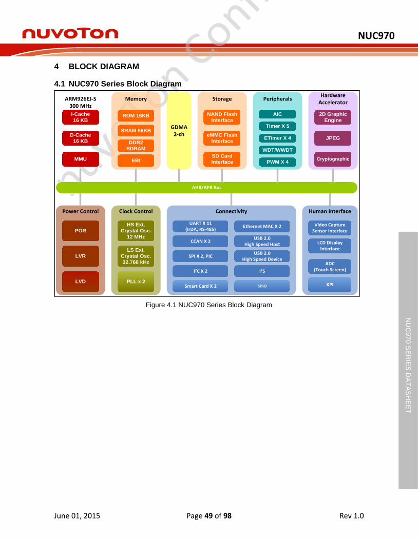
NUC970
June 01, 2015 Page 49 of 98 Rev 1.0
NU
C97
0 S
ER
IES
DA
TA
SH
EE
T
4 BLOCK DIAGRAM
4.1 NUC970 Series Block Diagram
ARM926EJ-S300 MHz
GDMA2-ch
Power Control Clock Control Connectivity
AHB/APB Bus
Memory
I-Cache
16 KB
D-Cache
16 KB
MMU
ROM 16KB
EBI
DDR2
SDRAM
SRAM 56KB
POR
HS Ext.
Crystal Osc.
12 MHz
LVR
LS Ext.
Crystal Osc.
32.768 kHz
PLL x 2
UART X 11(IrDA, RS-485)
I2SI2C X 2
SPI X 2, PIC
CCAN X 2
USB 2.0High Speed Device
USB 2.0 High Speed Host
Ethernet MAC X 2
Smart Card X 2 SDIO
Human Interface
Video CaptureSensor Interface
KPI
ADC(Touch Screen)
LCD Display Interface
Peripherals
AIC
Storage
NAND Flash
Interface
SD Card
Interface
Hardware Accelerator
2D Graphic
Engine
eMMC Flash
Interface
PWM X 4
WDT/WWDT
Timer X 5
ETimer X 4
Cryptographic
JPEG
LVD
Figure 4.1 NUC970 Series Block Diagram

NUC970
June 01, 2015 Page 50 of 98 Rev 1.0
NU
C97
0 S
ER
IES
DA
TA
SH
EE
T
5 FUNCTIONAL DESCRIPTION
5.1 ARM® ARM926EJ-S CPU Core
5.1.1 Overview
The ARM926EJ-S CPU core is a member of the ARM9 family of general-purpose microprocessors. The ARM926EJ-S CPU core is targeted at multi-tasking applications where full memory management, high performance, and low power are all important.
The ARM926EJ-S CPU core supports the 32-bit ARM and 16-bit Thumb instruction sets, enabling the user to choose between high performance and high code density. The ARM926EJ-S CPU core includes features for efficient execution of Java byte codes, providing Java performance similar to JIT, but without the associated code overhead.
The ARM926EJ-S processor provides support for external coprocessor enabling floating-point or other application-specific hardware acceleration to be added. The ARM926EJ-S CPU core implements ARM architecture version 5TEJ.
The ARM926EJ-S processor has a Harvard cached architecture and provides a complete high-performance processor subsystem, including:
An ARM9EJ-S integer core.
A Memory Management Unit (MMU).
Separate instruction and data cache.
Separate instruction and data AMBA AHB bus interfaces.

NUC970
June 01, 2015 Page 51 of 98 Rev 1.0
NU
C97
0 S
ER
IES
DA
TA
SH
EE
T
5.2 System Manager
5.2.1 Overview
The system management describes following information and functions.
System Resets
System Power Architecture
System Memory Map
System management registers for Product Identifier (PDID), Power-On Setting, System Wake-Up, Reset Control for on-chip controllers/peripherals, and multi-function pin control.
System Control registers
5.3 Clock Controller (CLK_CTL)
5.3.1 Overview
The clock controller generates all clocks for Video, Audio, CPU, AMBA and all the engine modules. This chip includes two PLL modules. The clock source for each module comes from the PLL, or from the external crystal input directly. For each clock there is bit on the CLKEN register to control the clock ON or OFF individually, and the divider setting is on the CLK_DIVCTL register. The register can also be used to control the clock enable or disable for power control.
5.3.2 Features
Supports two PLLs, up to 500 MHz, for high performance system operation
External 12 MHz high speed crystal input for precise timing operation
External 32.768 kHz low speed crystal input for RTC function and low speed clock source
5.4 Advanced Interrupt Controller (AIC)
5.4.1 Overview
An interrupt temporarily changes the sequence of program execution to react to a particular event such as power failure, watchdog timer timeout, transmit/receive request from Ethernet MAC Controller, and so on. The CPU processor provides two modes of interrupt, the Fast Interrupt (FIQ) mode for critical session and the Interrupt (IRQ) mode for general purpose. The IRQ request is occurred when the nIRQ input is asserted. Similarly, the FIQ request is occurred when the nFIQ input is asserted. The FIQ has privilege over the IRQ and can preempt an ongoing IRQ. It is possible to ignore the FIQ and the IRQ by setting the F and I bits in the current program status register (CPSR).
The Advanced Interrupt Controller (AIC) is capable of processing the interrupt requests up to 64 different sources. Currently, 61 interrupt sources are defined. Each interrupt source is uniquely assigned to an interrupt channel. For example, the watchdog timer interrupt is assigned to channel 1. The AIC implements a proprietary eight-level priority scheme that categories the available 61 interrupt sources into eight priority levels. Interrupt sources within the priority level 0 is the highest priority and the priority level 7 is the lowest. In order to make this scheme work properly, a certain priority level
NUC970
June 01, 2015 Page 52 of 98 Rev 1.0
NU
C97
0 S
ER
IES
DA
TA
SH
EE
T
must be specified to each interrupt source during power-on initialization; otherwise, the system shall behave unexpectedly. Within each priority level, interrupt source that is positioned in a lower channel has a higher priority. Interrupt source that is active, enabled, and positioned in the lowest channel with priority level 0 is promoted to the FIQ. Interrupt sources within the priority levels other than 0 are routed to the IRQ. The IRQ can be preempted by the occurrence of the FIQ. Interrupt nesting is performed automatically by the AIC.
Though interrupt sources originated from the chip itself are intrinsically high-level sensitive, the AIC can be configured as either low-level sensitive, high-level sensitive, negative-edge triggered, or positive-edge triggered to each interrupt source.
5.4.2 Features
AMBA APB bus interface
External interrupts can be programmed as either edge-triggered or level-sensitive
External interrupts can be programmed as either low-active or high-active
Flags to reflect the status of each interrupt source
Individual mask for each interrupt source
Support proprietary 8-level interrupt scheme to employ the priority scheme.
Priority methodology is adopted to allow for interrupt daisy-chaining
Automatically masking out the lower priority interrupt during interrupt nesting
Automatically clearing the interrupt flag when the external interrupt source is programmed to be edge-triggered
5.5 SDRAM Interface Controller (SDIC)
5.5.1 Overview
The SDRAM Controller support DDR2 type SDRAM. Only 16-bit data bus width is supported.
The SDRAM controller interface to three isolated AHB. All these AHB masters can access the memory independent. Except the memory access, the masters of AHB also could access the SDRAM control registers.
For performance and function issue, the SDRAM controller also supports the proprietary Enhanced-AHB. The EAHB add the down-count address mode, byte-enable signal and explicit burst access number. The explicit access number function is reached by modify the HBURST signal to EHBURST and it represent the access number. The maximum EAHB access number is 16. The SDRAM controller also builds a BIST module to test the external memory device.
An internal arbiter is used to schedule the access from the masters and the BIST request, the BIST request with the highest priority and the then the AHB3 master, AHB2 master and AHB1 master.
The SDRAM controller uses 3 pipe queues to improve the SDRAM command and data bus efficiency. The request in queue0 is the SDRAM active data access request. Simultaneous, the requests in queue1 can request the controller to issue the ACTIVE or PRECHARGE command to reduce the access latency for the later command. The queue1 also can issue the READ or WRITE command to close the SDRAM command when advance pipe queue
The SDRAM refresh rate is programmable. The Refresh and Power-on control module generate the refresh request signal and SDRAM power on sequence. The SDRAM controller also supports software reset, SDRAM self refresh and auto power down function.

NUC970
June 01, 2015 Page 53 of 98 Rev 1.0
NU
C97
0 S
ER
IES
DA
TA
SH
EE
T
5.5.2 Features
Support DDR2 SDRAM
Clock speed up to 150 MHz
Support 16-bit data bus width
Memory size depended on embedded SDRAM configuration by different part number.
5.6 MTP Controller (MTP)
5.6.1 Overview
The MTP (Multi-Time Programmable) controller performs an easy way to use and program the 256-bit Key for IP Security Engine. There is a MTP EPROM in this chip, and it can be programmed 15 times. User can program 256-bit key and 8-bit user defined fields each time. The 256-bit key is program-only, and only can be used by IP Security Engine. User can use the 8-bit user defined field for special purpose. The MTP also supports a LOCK function to protect the content of programmed key and user defined field.
5.6.2 Features
Support MTP EPROM programming
256-bit Key and 8-bit user defined data field
Up to 15 times programming
Support LOCK function
5.7 External Bus Interface (EBI)
5.7.1 Overview
This chip supports External Bus Interface (EBI), which controls the access to the external memory (SRAM) and External I/O devices. The EBI has up to 5 chip select signals to select different devices with 10-bit address bus. It supports 8-bit and 16-bit external data bus width for each bank.
5.7.2 Features
Support SRAM and external I/O devices.
Support 8/16-bit data bus width.
Support 80 and 68 mode interface signals.
Support up to 5 chip selects for SRAM and external I/O devices.
Support programmable access cycle.
Support four 32-bit write buffers.
5.8 General Purpose I/O (GPIO)
NUC970
June 01, 2015 Page 54 of 98 Rev 1.0
NU
C97
0 S
ER
IES
DA
TA
SH
EE
T
5.8.1 Overview
The NUC970 series have up to 148 General-Purpose I/O (GPIO) pins and can be shared with other function pins depending on the chip configuration. These 148 pins are arranged in 10 ports named as PA, PB, PC, PD, PE, PF, PG, PH, PI and PJ. PA, PB, PD, PE, PF, PG, PH and PI have 16 pins on port, PC has 15 pins on port and PJ has 5 pins on port. Each of the 148 I/O pins is independent and can be easily configured by user to meet various system configurations and design requirements. After reset, all 148 I/O pins are configured in General-Purpose I/O Input mode.
When any of the 148 I/O pins used as a General-Purpose I/O, its I/O type can be configured by user individually as Input or Output mode. In Input mode, the input buffer type could be selected as CMOS
input buffer or Schmitt trigger input buffer. Each I/O pin also equips a pull-up resistor (45 k ~ 82 k)
and a pull-down resistor (37 k ~ 91 k). The enable of pull-up/pull-down resistor is controllable.
5.8.2 Features
Support input and output mode.
Support CMOS and Schmitt trigger input buffer.
Support controllable pull-up and pull-down resistor.
Support both edge and level interrupt.
Support de-bounce circuit to filter the noise.
5.9 General DMA Controller (GDMA)
5.9.1 Overview
The chip has a two-channel general DMA controller with or without descriptor fetch operation, called the GDMA. The two-channel GDMA performs the memory-to-memory data transfers without the CPU intervention:
The on-chip GDMA can be started by the software. Software can also be used to restart the GDMA operation after it has been stopped. The CPU can recognize the completion of a GDMA operation by software polling or when it receives an internal GDMA interrupt. The GDMA controller can increment source or destination address, decrement them as well, and conduct 8-bit (byte), 16-bit (half-word), or 32-bit (word) data transfers.
5.9.2 Features
AMBA AHB compliant
Descriptor and Non-Descriptor based function
Supports 8-data burst mode to boost performance
Provides support for external GDMA device
Demand mode speeds up external GDMA operations
5.10 Timer Controller (TMR)

NUC970
June 01, 2015 Page 55 of 98 Rev 1.0
NU
C97
0 S
ER
IES
DA
TA
SH
EE
T
5.10.1 Overview
The general timer controller includes five channels, TIMER0, TIMER1, TIMER2, TIMER3, and TIMER4, which allow user to easily implement a counting scheme or timing control for applications. The timer can perform functions like frequency measurement, event counting, interval measurement, pulse generation, delay timing, and so on. The timer possesses features such as adjustable resolution, programmable counting period, and detailed information. The timer can generate an interrupt signal upon timeout, or provide the current value of count during operation.
5.10.2 Features
Independent Clock Source for each Timer channel (TMRx_CLK, x= 0, 1, 2, 3, 4).
Five channels with a 24-bit up counter and an interrupt request each.
Internal 8-bit pre-scale counter.
Internal 24-bit up counter is readable through Timer Data Register, TDR (TMR_DR[23:0]).
Supports One-shot, Periodic, and Continuous operation mode.
Time-out period = (Period of timer clock input) * (8-bit pre-scale counter + 1) * (24-bit TCMP setting value).
Maximum counting time =
( ), if TMRx_CLK = 12 MHz.
5.11 Enhance Timer Controller (ETMR)
5.11.1 Overview
This chip is equipped with four enhance timer modules including ETIMER0, ETIMER1, ETIMER2 and ETIMER3, which allow user to easily implement a counting scheme or timing control for applications. The timer can perform functions like frequency measurement, event counting, interval measurement, clock generation, delay timing, and so on. The timer can generate an interrupt signal upon timeout, or provide the current value of count during operation.
5.11.2 Features
Independent Clock Enable Control for each Timer (ECLKetmr0, ECLKetmr1, ECLKetmr2 and ECLKetmr3)
Time-out period = (Period of timer clock input) * (8-bit pre-scale counter + 1) * (24-bit TCMP)
Counting cycle time = (1 / ECLKetmr) * (2^8) * (2^24)
Internal 8-bit pre-scale counter
Internal 24-bit up counter is readable through TDR (Timer Data Register)
Supports One-shot, Periodic, Output Toggle and Continuous Counting Operation mode
Supports external pin capture for interval measurement
Supports external pin capture for timer counter reset
5.12 Pulse Width Modulation (PWM)

NUC970
June 01, 2015 Page 56 of 98 Rev 1.0
NU
C97
0 S
ER
IES
DA
TA
SH
EE
T
5.12.1 Overview
This chip has one PWM controller, and it has 4 independent PWM outputs, CH0~CH3, or as 2 complementary PWM pairs, (CH0, CH1), (CH2, CH3) with 2 programmable dead-zone generators. Each PWM pair has one Prescaler, one clock divider, two clock selectors, two 16-bit PWM counters, two 16-bit comparators, and one Dead-Zone generator. They are all driven by APB system clock (PCLK) in chip. Each PWM channel can be used as a timer and issue interrupt independently.
Two channels PWM Timers in one pair share the same prescaler. The Clock divider provides each PWM channel with 5 divided clock sources (1, 1/2, 1/4, 1/8, 1/16). Each channel receives its own clock signal from clock divider which receives clock from 8-bit prescaler. The 16-bit down-counter in each channel receive clock signal from clock selector and can be used to handle one PWM period. The 16-bit comparator compares PWM counter value with threshold value in register CMR (PWM_CMR[15:0]) loaded previously to generate PWM duty cycle. The clock signal from clock divider is called PWM clock. Dead-Zone generator utilize PWM clock as clock source. Once Dead-Zone generator is enabled, two outputs of the corresponding PWM channel pair will be replaced by the output of Dead-Zone generator. The Dead-Zone generator is used to control off-chip power device.
To prevent PWM driving output pin with unsteady waveform, 16-bit down-counter and 16-bit comparator are implemented with double buffering feature. User can feel free to write data to counter buffer register and comparator buffer register without generating glitch. When 16-bit down-counter reaches zero, the interrupt request is generated to inform CPU that time is up. When counter reaches zero, if counter is set as periodic mode, it is reloaded automatically and start to generate next cycle. User can set PWM counter as one-shot mode instead of periodic mode. If counter is set as one-shot mode, counter will stop and generate one interrupt request when it reaches zero. The value of comparator is used for pulse width modulation. The counter control logic changes the output level when down-counter value matches the value of compare register.
5.12.2 Features
4 PWM channels with a 16-bit down counter and an interrupt each
2 complementary PWM pairs, (CH0, CH1), (CH2, CH3), with a programmable dead-zone generator each
Internal 8-bit prescaler and a clock divider for each PWM paired channel
Independent clock source selection for each PWM channel
Internal 16-bit down counter and 16-bit comparator for each independent PWM channel
PWM down-counter supports One-shot or Periodic mode
5.13 Watchdog Timer (WDT)
5.13.1 Overview
The purpose of Watchdog Timer (WDT) is to perform a system reset when system runs into an unknown state. This prevents system from hanging for an infinite period of time. Besides, this Watchdog Timer supports the function to wake-up system from Idle/Power-down mode.
5.13.2 Features
18-bit free running up counter for WDT time-out interval
Selectable time-out interval (24 ~ 2
18) and the time-out interval is 0.48828125 ms ~ 8 s if
WDT_CLK = 32.768 kHz
System kept in reset state for a period of (1 / WDT_CLK) * 63
NUC970
June 01, 2015 Page 57 of 98 Rev 1.0
NU
C97
0 S
ER
IES
DA
TA
SH
EE
T
Supports selectable WDT reset delay period, including 1026、130、18 or 3 WDT_CLK reset
delay period
Supports to force WDT enabled after chip powered on or reset by setting WDTON in PWRON register
Supports WDT time-out wake-up function only if WDT clock source is selected as 32 kHz
5.14 Windowed Watchdog Timer (WWDT)
5.14.1 Overview
The Window Watchdog Timer (WWDT) is used to perform a system reset within a specified window period to prevent software run to uncontrollable status by any unpredictable condition.
5.14.2 Features
6-bit down counter value (CNTDAT) and 6-bit compare value (CMPDAT) to make the WWDT time-out window period flexible.
Supports 4-bit value (PSCSEL) to programmable maximum 11-bit prescale counter period of WWDT counter.
NUC970
June 01, 2015 Page 58 of 98 Rev 1.0
NU
C97
0 S
ER
IES
DA
TA
SH
EE
T
5.15 Real Time Clock (RTC)
5.15.1 Overview
The Real Time Clock (RTC) controller provides the real time clock and calendar information. The clock source of RTC controller is from an external 32.768 kHz low-speed crystal which connected at pins X32_IN and X32_OUT (refer to pin Description). The RTC controller provides the real time clock (hour, minute, second) in RTC_TIME (RTC Time Loading Register) as well as calendar information (year, month, day) in RTC_CAL (RTC Calendar Loading Register). It also offers RTC alarm function that user can preset the alarm time in RTC_TALM (RTC Time Alarm Register) and alarm calendar in RTC_CALM (RTC Calendar Alarm Register). The data format of RTC time and calendar message are all expressed in BCD (Binary Coded Decimal) format.
The RTC controller supports periodic RTC Time Tick and Alarm Match interrupts. The periodic RTC Time Tick interrupt has 8 period interval options 1/128, 1/64, 1/32, 1/16, 1/8, 1/4, 1/2 and 1 second which are selected by RTC_TICK (RTC_TICK[2:0] Time Tick Register). When real time and calendar message in RTC_TIME and RTC_CAL are equal to alarm time and calendar settings in RTC_TALM and RTC_CALM, the ALMIF (RTC_INTSTS [0] RTC Alarm Interrupt Flag) is set to 1 and the RTC alarm interrupt signal is generated if the ALMIEN (RTC_INTEN [0] Alarm Interrupt Enable) is enabled.
Both RTC Time Tick and Alarm Match interrupt signal can cause chip to wake-up from Idle or Power-down mode if the corresponding interrupt enable bit (ALMIEN or TICKIEN) is set to 1 before chip enters Idle or Power-down mode.
Real Time Clock (RTC) block can operate with independent power supply (RTC_VDD) while the system power is off.
5.15.2 Features
Supports real time counter and calendar counter for RTC time and calendar check.
Supports time (hour, minute, second) and calendar (year, month, day) alarm and alarm mask settings.
Selectable 12-hour or 24-hour time scale.
Supports Leap Year indication.
Supports Day of the Week counter.
Supports frequency compensation mechanism for 32.768 kHz clock source.
All time and calendar message expressed in BCD format.
Supports periodic RTC Time Tick interrupt with 8 period interval options 1/128, 1/64, 1/32, 1/16, 1/8, 1/4, 1/2 and 1 second.
Supports RTC Time Tick and Alarm match interrupt.
Supports chip wake-up from Idle or Power-down mode while alarm or relative alarm interrupt is generated.
Supports 64 bytes spare registers to store user’s important information.
Supports power on/off control mechanism to control system core power.
NUC970
June 01, 2015 Page 59 of 98 Rev 1.0
NU
C97
0 S
ER
IES
DA
TA
SH
EE
T
5.16 UART Interface Controller (UART)
This chip equips up to eleven channels of Universal Asynchronous Receiver/Transmitters (UART). UART1/2/4/6/8/10 supports High-speed UART and UART0/3/5/7/9 perform Normal Speed UART, besides, all the UART channels support flow control function. The UART controller also supports IrDA (SIR), LIN Master/Slave and RS-485 function modes.
5.16.1 Overview
The Universal Asynchronous Receiver/Transmitter (UART) performs a serial-to-parallel conversion on data received from the peripheral, and a parallel-to-serial conversion on data transmitted from the CPU.
Each UART channel supports seven types of interrupts including (1). transmitter FIFO empty interrupt (INT_THRE), (2). receiver threshold level reaching interrupt (INT_RDA), (3). line status interrupt (parity error or framing error or break interrupt) (INT_RLS), (4). receiver buffer time-out interrupt (INT_TOUT), (5). MODEM/Wake-up status interrupt (INT_MODEM), (6). Buffer error interrupt (INT_BUF_ERR), and (7). LIN interrupt (INT_LIN).
The UART1/ 2/ 4/ 6/ 8/ 10 is built-in with a 64-byte transmitter FIFO (TX_FIFO) and a 64-byte receiver FIFO (RX_FIFO) that reduces the number of interrupts presented to the CPU and the UART0/ 3/ 5/ 7/ 9 are equipped 16-byte transmitter FIFO (TX_FIFO) and 16-byte receiver FIFO (RX_FIFO). The CPU can read the status of the UART at any time during the operation. The reported status information includes the type and condition of the transfer operations being performed by the UART, as well as 4 error conditions (parity error, framing error, break interrupt and buffer error) probably occur while receiving data.
The UART includes a programmable baud rate generator that is capable of dividing clock input by divisors to produce the serial clock that transmitter and receiver need.
All of the controllers support auto-flow control function that uses two low-level signals, /CTS (clear-to-send) and /RTS (request-to-send), to control the flow of data transfer between the UART and external devices (ex: Modem). When auto-flow is enabled, the UART is not allowed to receive data until the UART asserts /RTS to external device. When the number of bytes in the RX FIFO equals the value of RTS_TRI_LEV (UA_FCR [19:16]), the /RTS is de-asserted. The UART sends data out when UART controller detects /CTS is asserted from external device. If a valid asserted /CTS is not detected the UART controller will not send data out.
The UART controllers also provides Serial IrDA (SIR, Serial Infrared) function (The IrDA mode is selected by setting the (FUN_SEL(UA_FUN_SEL[2:0]) = 010) to select IrDA function). The SIR specification defines a short-range infrared asynchronous serial transmission mode with one start bit, 8 data bits, and 1 stop bit. The maximum data rate is 115.2 Kbps (half duplex). The IrDA SIR block contains an IrDA SIR Protocol encoder/decoder. The IrDA SIR protocol is half-duplex only. So it cannot transmit and receive data at the same time. The IrDA SIR physical layer specifies a minimum 10ms transfer delay between transmission and reception. This delay feature must be implemented by software.
The alternate function of UART controllers is LIN (Local Interconnect Network) function. The LIN mode is selected by setting the (FUN_SEL(UA_FUN_SEL[2:0]) = 001) to select LIN mode. In LIN mode, one start bit and 8-bit data format with 1-bit stop bit are required in accordance with the LIN standard.
For the NUC970 series, another alternate function of UART controllers is RS-485 9-bit mode function, and direction control provided by RTS pin to implement the function by software. The RS-485 mode is selected by setting the (FUN_SEL(UA_FUN_SEL[2:0]) = 011) to select RS-485 function. The RS-485 driver control is implemented using the RTS control signal from an asynchronous serial port to enable the RS-485 driver. In RS-485 mode, many characteristics of the RX and TX are the same as UART.
NUC970
June 01, 2015 Page 60 of 98 Rev 1.0
NU
C97
0 S
ER
IES
DA
TA
SH
EE
T
5.16.2 Features
Full duplex, asynchronous communications
Separate receive / transmit 64/16 bytes entry FIFO for data payloads
Supports hardware auto flow control/flow control function (CTS, RTS) and programmable RTS flow control trigger level
Programmable receiver buffer trigger level
Supports programmable baud-rate generator for each channel individually
Supports CTS wake-up function
Supports 8-bit receiver buffer time-out detection function
Programmable transmitting data delay time between the last stop and the next start bit by setting DLY(UA_TOR[15:8]) register
Supports break error, frame error, parity error and receive / transmit buffer overflow detect function
Fully programmable serial-interface characteristics
Programmable number of data bit, 5-, 6-, 7-, 8-bit character
Programmable parity bit, even, odd, no parity or stick parity bit generation and detection
Programmable stop bit, 1, 1.5, or 2 stop bit generation
Supports IrDA SIR function mode
Supports LIN function mode
Supports RS-485 function mode
5.17 Smart Card Host Interface (SC)
5.17.1 Overview
The Smart Card Interface controller (SC controller) is based on ISO/IEC 7816-3 standard and fully compliant with PC/SC Specifications. It also provides status of card insertion/removal.
5.17.2 Features
ISO-7816-3 T = 0, T = 1 compliant
EMV2000 compliant
Up to two ISO-7816-3 ports
Separates receive/transmit 4 byte entry FIFO for data payloads
Programmable transmission clock frequency
Programmable receiver buffer trigger level
Programmable guard time selection (11 ETU ~ 267 ETU)
A 24-bit and two 8-bit timers for Answer to Request (ATR) and waiting times processing
Supports auto inverse convention function
Supports transmitter and receiver error retry and error number limiting function
NUC970
June 01, 2015 Page 61 of 98 Rev 1.0
NU
C97
0 S
ER
IES
DA
TA
SH
EE
T
Supports hardware activation sequence, hardware warm reset sequence and hardware deactivation sequence process
Supports hardware auto deactivation sequence when detected the card removal
Supports UART mode
Full duplex, asynchronous communications
Separates receiving / transmitting 4 bytes entry FIFO for data payloads
Supports programmable baud rate generator for each channel
Supports programmable receiver buffer trigger level
Programmable transmitting data delay time between the last stop bit leaving the TX-FIFO and the de-assertion by setting EGT (SC_EGT[7:0])
Programmable even, odd or no parity bit generation and detection
Programmable stop bit, 1- or 2- stop bit generation
5.18 I2C Synchronous Serial Interface Controller (I
2C)
5.18.1 Overview
I2C is a two-wire, bi-directional serial bus that provides a simple and efficient method of data
exchange between devices. The I2C standard is a true multi-master bus including collision
detection and arbitration that prevents data corruption if two or more masters attempt to control the bus simultaneously.
Serial, 8-bit oriented bi-directional data transfers can be up to 100 KBit/s in Standard-mode, 400 KBit/s in the Fast-mode, or 3.4 Mbit/s in the High-speed mode. Only 100kbps and 400kbps modes are supported directly in this chip.
Data transfer is synchronized to SCL signal between a Master and a Slave with byte-by-byte basis. Each data byte is 8 bits long. There is one SCL clock pulse for each data bit with the MSB being transmitted first. An acknowledge bit follows each transferred byte. Each bit is sampled during the high period of SCL; therefore, the SDA line may be changed only during the low period of SCL and must be held stable during the high period of SCL. A transition on the SDA line while SCL is high is interpreted as a command (START or STOP).
5.18.2 Features
Compatible with Philips I2C standard, support master mode
Multi Master Operation.
Clock stretching and wait state generation.
Provide multi-byte transmit operation, up to 4 bytes can be transmitted in a single transfer
Software programmable acknowledge bit.
Arbitration lost interrupt, with automatic transfer cancellation.
Start/Stop/Repeated Start/Acknowledge generation.
Start/Stop/Repeated Start detection.
Bus busy detection.
Supports 7 bit addressing mode.
Fully static synchronous design with one clock domain.

NUC970
June 01, 2015 Page 62 of 98 Rev 1.0
NU
C97
0 S
ER
IES
DA
TA
SH
EE
T
Software mode I2C.
5.19 SPI Interface Controller (SPI)
5.19.1 Overview
The SPI is a synchronous serial interface performs a serial-to-parallel conversion on data characters received from the peripheral, and a parallel-to-serial conversion on data characters received from CPU. This interface can drive up to 2 external peripherals and is seen as the master.
5.19.2 Features
Support master mode
Full duplex synchronous serial data transfer
Variable length of transfer word up to 32 bits
Provide burst mode operation, transmit/receive can be executed up to four times in one transfer
MSB or LSB first data transfer
Rx and Tx on both rising or falling edge of serial clock independently
Support 2 slave/device select lines
Support dual IO and quad mode for SPI flash access
5.20 I2S Controller (I
2S)
5.20.1 Overview
The I2S controller consists of I
2S and PCM protocols to interface with external audio CODEC. The I
2S
and PCM interface supports 8, 16, 18, 20 and 24-bit left/right precision in record and playback. When operating in 18/20/24-bit precision, each left/right-channel sample is stored in a 32-bit word. Each left/right-channel sample has 24/20/18 MSB bits of valid data and other LSB bits are the padding zeros. When operating in 16-bit precision, right-channel sample is stored in MSB of a 32-bit word and left-channel sample is stored in LSB of a 32-bit word.
The following are the property of the DMA.
When 16-bit precision, the DMA always 8-beat incrementing burst (FIFO_TH = 0) or 4-beat incrementing burst (FIFO_TH = 1).
When 24/20/18-bit precision, the DMA always 16-beat incrementing burst (FIFO_TH = 0) or 8-beat incrementing burst (FIFO_TH = 1).
Always bus lock when 4-beat or 8-beat or 16-beat incrementing burst.
When reach eighth, quarter, middle and end address of destination address, a DMA_IRQ is triggered to CPU automatically.
An AHB master port and an AHB slave port are offered in I2S controller.
5.20.2 Features
Support I2S interface record and playback
Left/right channel

NUC970
June 01, 2015 Page 63 of 98 Rev 1.0
NU
C97
0 S
ER
IES
DA
TA
SH
EE
T
8, 16, 20, 24-bit data precision
Mater and slave mode
Support PCM interface record and playback
Two slots
8, 16, 20, 24-bit data precision
Master mode
Use DMA to playback and record data, with interrupt
Support two addresses for left/right channel data and different slots
5.21 Ethernet MAC Controller (EMAC)
5.21.1 Overview
This chip provides 2 Ethernet MAC Controller (EMAC) for Network application.
The Ethernet MAC controller consists of IEEE 802.3/Ethernet protocol engine with internal CAM function for recognizing Ethernet MAC addresses; Transmit-FIFO, Receive-FIFO, TX/RX state machine controller, time stamping engine for IEEE 1588, Magic Packet parsing engine and status controller.
The EMAC supports RMII (Reduced MII) interface to connect with external Ethernet PHY.
5.21.2 Features
Supports IEEE Std. 802.3 CSMA/CD protocol
Supports Ethernet frame time stamping for IEEE Std. 1588 – 2002 protocol
Supports both half and full duplex for 10 Mbps or 100 Mbps operation
Supports RMII interface
Supports MII Management function to control external Ethernet PHY
Supports pause and remote pause function for flow control
Supports long frame (more than 1518 bytes) and short frame (less than 64 bytes) reception
Supports 16 entries CAM function for Ethernet MAC address recognition
Supports Magic Packet recognition to wake system up from power-down mode
Supports 256 bytes transmit FIFO and 256 bytes receive FIFO
Supports DMA function
5.22 USB 2.0 Device Controller (USBD)
5.22.1 Overview
The USB device controller interfaces the AHB bus and the UTMI bus. The USB controller contains both the AHB master interface and AHB slave interface. CPU programs the USB controller registers through the AHB slave interface. For IN or OUT transfer, the USB device controller needs to write data to memory or read data from memory through the AHB master interface. The USB device controller is complaint with USB 2.0 specification and it contains 12 configurable endpoints in addition to control
NUC970
June 01, 2015 Page 64 of 98 Rev 1.0
NU
C97
0 S
ER
IES
DA
TA
SH
EE
T
endpoint. These endpoints could be configured to BULK, INTERRUPT or ISO. The USB device controller has a built-in DMA to relieve the load of CPU.
5.22.2 Features
USB Specification reversion 2.0 compliant
Supports 12 configurable endpoints in addition to Control Endpoint
Each of the endpoints can be Isochronous, Bulk or Interrupt and either IN or OUT direction
Three different operation modes of an in-endpoint - Auto Validation mode, Manual
Validation mode, Fly mode
Supports DMA operation
4096 Bytes Configurable RAM used as endpoint buffer
Supports Endpoint Maximum Packet Size up to 1024 bytes
5.23 USB Host Controller (USBH)
5.23.1 Overview
The Universal Serial Bus (USB) is a fast, bi-directional, isochronous, low-cost, dynamically attachable serial interface standard intended for modem, scanners, PDAs, keyboards, mice, and digital imaging devices. The USB is a 4-wire serial cable bus that supports serial data exchange between a Host Controller and a network of peripheral devices. The attached peripherals share USB bandwidth through a host-scheduled, token-based protocol. Peripherals may be attached, configured, used, and detached, while the host and other peripherals continue operation (i.e. hot plug and unplug is supported).
5.23.2 Features
Fully compliant with USB Revision 2.0 specification.
Enhanced Host Controller Interface (EHCI) Revision 1.0 compatible.
Open Host Controller Interface (OHCI) Revision 1.0 compatible.
Supports high-speed (480Mbps), full-speed (12Mbps) and low-speed (1.5Mbps) USB devices.
Supports Control, Bulk, Interrupt, Isochronous and Split transfers.
Integrated a port routing logic to route full/low speed device to OHCI controller.
Built-in DMA for real-time data transfer.
5.24 Controller Area Network (CAN)
5.24.1 Overview
The C_CAN consists of the CAN Core, Message RAM, Message Handler, Control Registers and Module Interface. The CAN Core performs communication according to the CAN protocol version 2.0 part A and B. The bit rate can be programmed to values up to 1MBit/s. For the connection to the physical layer, additional transceiver hardware is required.
For communication on a CAN network, individual Message Objects are configured. The Message

NUC970
June 01, 2015 Page 65 of 98 Rev 1.0
NU
C97
0 S
ER
IES
DA
TA
SH
EE
T
Objects and Identifier Masks for acceptance filtering of received messages are stored in the Message RAM. All functions concerning the handling of messages are implemented in the Message Handler. These functions include acceptance filtering, the transfer of messages between the CAN Core and the Message RAM, and the handling of transmission requests as well as the generation of the module interrupt.
The register set of the C_CAN can be accessed directly by the software through the module interface. These registers are used to control/configure the CAN Core and the Message Handler and to access the Message RAM.
5.24.2 Features
Supports CAN protocol version 2.0 part A and B
Bit rates up to 1 MBit/s
32 Message Objects
Each Message Object has its own identifier mask
Programmable FIFO mode (concatenation of Message Objects)
Maskable interrupt
Disabled Automatic Re-transmission mode for Time Triggered CAN applications
Programmable loop-back mode for self-test operation
16-bit module interfaces to the AMBA APB bus
Supports wake-up function
5.25 Flash Memory Interface (FMI)
5.25.1 Overview
The Flash Memory Interface (FMI) of this Chip has DMA unit and FMI unit. The DMA unit provides a DMA (Direct Memory Access) function for FMI to exchange data between system memory (ex. SDRAM) and shared buffer (128 bytes), and the FMI unit control the interface of eMMC or NAND flash. The interface controller can support eMMC and NAND-type flash and the FMI is cooperated with DMAC to provide a fast data transfer between system memory and cards.
5.25.2 Features:
Support single DMA channel and address in non-word boundary.
Support hardware Scatter-Gather function.
Support 128Bytes shared buffer for data exchange between system memory and flash device. (Separate into two 64 bytes ping-pong FIFO).
Support eMMC Flash device.
Supports SLC and MLC NAND type Flash.
Adjustable NAND page sizes. (512B+spare area, 2048B+spare area, 4096B+spare area and 8192B+spare area).
Support up to 4bit/8bit/12bit/15bit/24bit hardware ECC calculation circuit to protect data communication.
NUC970
June 01, 2015 Page 66 of 98 Rev 1.0
NU
C97
0 S
ER
IES
DA
TA
SH
EE
T
Support programmable NAND timing cycle.
5.26 Secure Digital Host Controller (SDH)
5.26.1 Overview
The Secure-Digital Card Host Controller (SDH) equips DMAC unit and SD unit. The DMAC unit provides a DMA (Direct Memory Access) function for SD to exchange data between system memory and shared buffer (128 bytes), and the SD unit controls the interface of SD/SDHC/SDIO. The SDH controller supports SD/SDHC/SDIO card and cooperates with DMAC to provide a fast data transfer between system memory and cards.
5.26.2 Features
Supports single DMA channel
Supports hardware Scatter-Gather functionality.
Supports 128 Bytes shared buffer for data exchange between system memory and cards.
Supports SD, SDHC and SDIO card.
NUC970
June 01, 2015 Page 67 of 98 Rev 1.0
NU
C97
0 S
ER
IES
DA
TA
SH
EE
T
5.27 Cryptographic Accelerator (CRYPTO)
5.27.1 Overview
The Crypto (Cryptographic Accelerator) includes a secure pseudo random number generator (PRNG) core and supports AES, DES/TDES, SHA and HMAC algorithms.
The PRNG core supports 64 bits, 128 bits, 192 bits, and 256 bits random number generation.
The AES accelerator is an implementation fully compliant with the AES (Advance Encryption Standard) encryption and decryption algorithm. The AES accelerator supports ECB, CBC, CFB, OFB, CTR, CBC-CS1, CBC-CS2, and CBC-CS3 mode.
The DES/TDES accelerator is an implementation fully compliant with the DES and Triple DES encryption/decryption algorithm. The DES/TDES accelerator supports ECB, CBC, CFB, OFB, and CTR mode.
The SHA accelerator is an implementation fully compliant with the SHA-160, SHA-224, SHA-256, SHA-384, and SHA-512 and corresponding HMAC algorithms.
5.27.2 Features
PRNG
Supports 64 bits, 128 bits , 192 bits, and 256 bits random number generation
AES
Supports FIPS NIST 197
Supports SP800-38A and addendum
Supports 128, 192, and 256 bits key
Supports both encryption and decryption
Supports ECB, CBC, CFB, OFB , CTR, CBC-CS1, CBC-CS2, and CBC-CS3 mode
Supports key expander
DES
Supports FIPS 46-3
Supports both encryption and decryption
Supports ECB, CBC, CFB, OFB, and CTR mode
TDES
Supports FIPS NIST 800-67
Implemented according to the X9.52 standard
Supports two keys or three keys mode
Supports both encryption and decryption
Supports ECB, CBC, CFB, OFB, and CTR mode
SHA
Supports FIPS NIST 180, 180-2
Supports SHA-160, SHA-224, SHA-256, SHA-384, and SHA-512
HMAC

NUC970
June 01, 2015 Page 68 of 98 Rev 1.0
NU
C97
0 S
ER
IES
DA
TA
SH
EE
T
Supports FIPS NIST 180, 180-2
Supports HMAC-SHA-160, HMAC-SHA-224, HMAC-SHA-256, HMAC-SHA-384, and HMAC-SHA-512
5.28 2D Graphic Engine (GE2D)
5.28.1 Overview
A 32-bit 2D Graphics Engine (GE2D) is specially designed to improve the performance of graphic processing. It can accelerate the operation of individual GUI functions such as BitBLTs and Bresenham Line Draw to operate at all pixel depths including 8/16/32 bit-per-pixel.
A pixel is the smallest addressable screen element as defined in Microsoft Windows, and lines and pictures are made up by a variety of pixels. GE2D is used to speed up graphic performance in pixel data moving and line drawing, as well as to accelerate almost all computer graphic Boolean operations by eliminating the CPU overhead. Meanwhile, the functions of rotation and scaling down are implemented for some special applications. In image scaling down function, both programmable horizontal and vertical N/M scaling down factors are provided for resizing the image. For the 2D rotation, it can rotate left or right 45, 90 or 180 degrees, and also supports the flip/flop, mirror or up-side-down pictures.
5.28.2 Features
Support 2D Bit Block Transfer (BitBLT) functions defined in Microsoft GDI
Support Host BLT
Support Pattern BLT
Support Color/Font Expanding BLT
Support Transparent BLT
Support Tile BLT
Support Block Move BLT
Support Copy File BLT
Support Color/Font Expansion
Support Rectangle Fill
Support RGB332/RGB565/RGB888 data format.
Support fore/background colors and all Microsoft 256 ternary raster-operation codes (ROP)
Support both inside and outside clipping function
Support alpha-blending for source/destination picture overlaying
Support fast Bresenham line drawing algorithm to draw solid/textured line
Support rectangular border and frame drawing
Support picture re-sizing
Support down-scaling from 1/255 to 254/255
Support up-scaling from 1 to 1.996 (1+254/255)
Support object rotation with different degree
Support L45 (45 degree left rotation) and L90 (90 degree left rotation)

NUC970
June 01, 2015 Page 69 of 98 Rev 1.0
NU
C97
0 S
ER
IES
DA
TA
SH
EE
T
Support R45 (45 degree right rotation) and R90 (90 degree right rotation)
Support M180 (mirror/flop)
Support F180 (up-side-down (flip) and X180 (180 degree rotation)
5.29 JPEG Codec (JPEG)
5.29.1 Overview
The JPEG Codec supports Baseline Sequential Mode JPEG still image compression and decompression that is fully compliant with ISO/IEC International Standard 10918-1 (T.81). The features and capability of the JPEG codec are listed below.
5.29.2 Features
If image data input or output by planar format (PLANAR_ON (JITCR[15])= 1), the features are as following:
Support to encode interleaved YCbCr 4:2:2/4:2:0 and gray-level (Y only) format image
Support to decode interleaved YCbCr 4:4:4/4:2:2/4:2:0/4:1:1 and gray-level (Y only) format image
Support to decode YCbCr 4:2:2 transpose format
The encoded JPEG bit-stream format is fully compatible with JFIF and EXIF standards
Support arbitrary width and height image encode and decode (up to 8192x8192)
Support three programmable quantization-tables
Support standard default Huffman-table and programmable Huffman-table for decode
Support arbitrarily 1X~8X image up-scaling function for encode mode
Support down-scaling function for encode and decode modes(Thumbnail/Primary)
Support specified window decode mode
Support quantization-table adjustment for bit-rate and quality control in encode mode
Support rotate function in encode mode
If image data input or output by packet format (PLANAR_ON (JITCR[15])= 0), the feature are as following:
Support to encode interleaved YUYV format input image, output bitstream 4:2:2 and 4:2:0 format
Support to decode interleaved YCbCr 4:4:4/4:2:2/4:2:0 format image
Support decoded output image YUYV422, RGB555, RGB565, RGB888 format (ORDER= 1).
The encoded JPEG bit-stream format is fully compatible with JFIF and EXIF standards
Support arbitrary width and height image encode and decode(Primary Only)
Support three programmable quantization-tables
Support standard default Huffman-table and programmable Huffman-table for decode
Support arbitrarily 1X~8X image up-scaling function for encode mode
Support down-scaling function 1X~ 16X for Y422 and Y420, 1X~ 8X for Y444 for decode mode

NUC970
June 01, 2015 Page 70 of 98 Rev 1.0
NU
C97
0 S
ER
IES
DA
TA
SH
EE
T
Support specified window decode mode
Support quantization-table adjustment for bit-rate and quality control in encode mode
5.30 LCD Display Interface Controller (LCM)
5.30.1 Overview
The main purpose of Display Controller is used to display the video/image data to LCD device or connect with external TV-encoder. The video/image data source may come from the image sensor, JPEG decoder and the OSD pattern which have been stored in system memory (SDRAM). The input data format of the display controller can be packet YUV422, packet YUV444, packet RGB444, packet RGB565, packet RGB666, and packet RGB888. The OSD (On Screen Display) function supports packet YUV422 and 8/16/24-bit direct-color mode. The LCD controller supports both sync-type and MPU-type LCDM. This LCD Controller is a bus master and can transfer display data from system memory (SDRAM) without CPU intervention.
5.30.2 Features
Input data format
YUV422, YUV444
RGB444, RGB565, RGB666, RGB888
Output format
YUV422, YUV444
RGB444, RGB565, RGB666, RGB888
Input size: Maximum size 1024 * 768
Image resize
Horizontal up-scaling 1~8X in fractional steps
Vertical up-scaling 1~8X in fractional steps
Convert full range YUV to CCIR601
Windowing support for three OSD graphic or text overlay
Support CCIR-656 (with header), CCIR-601(with hsync and vsync) 8/16-bit YUV data output format to connect with external TV encoder
Support both sync-type and MPU-type LCM (with v-sync or not)
Support the 8/9/16/18/24-bit data output to connect with 80/68 series MPU type LCM module
The LCD Controller includes the following main functions:
Video post-processing
Display & overlay control
Video output control
Hardware cursor control
5.31 Capture Sensor Interface Controller (CAP)

NUC970
June 01, 2015 Page 71 of 98 Rev 1.0
NU
C97
0 S
ER
IES
DA
TA
SH
EE
T
5.31.1 Overview
The Image Capture Interface is designed to capture image data from a sensor. After capturing or fetching image data, it will process the image data, and then FIFO output them into frame buffer.
5.31.2 Feature
8-bit RGB565 sensor
8-bit YUV422 sensor
Supports CCIR601 YCbCr color range scale to full YUV color range
Supports 4 packaging format for packet data output: YUYV, Y only, RGB565, RGB555
Supports YUV422 planar data output
Supports the CROP function to crop input image to the required size for digital application.
Supports the down scaling function to scale input image to the required size for digital application.
Supports frame rate control
Supports field detection and even/odd field skip mechanism
Supports packet output dual buffer control through hardware buffer controller
Supports negative/sepia/posterization color effect
Supports two independent capture interfaces
5.32 Analog to Digital Converter (ADC)
5.32.1 Overview
The NUC9xx series contains one 12-bit Successive Approximation Register analog-to-digital converter (SAR A/D converter) with eight input channels. The A/D converter supports two operation modes: 4-wire or 5-wire mode. The ADC is especially suitable to act as touch screen controller. Battery voltage detection could be easily accomplished by the SAR ADC. It has keypad interrupt signal generator.
5.32.2 Features
Resolution: 12-bit resolution.
DNL: +/-1.5 LSB, INL: +/-3 LSB.
Dual Data Rates: 1MSPS/200KSPS.
Analog Input Range: VREF to AGND, could be rail-to-rail.
Analog Supply: 2.7-3.6V.
Digital Supply: 1.2V.
8 Single-Ended Analog inputs.
Compatible with 4-wire or 5-wire Touch Screen Interface.
Touch Pressure Measurement for 4-wire touch screen application.
Direct Battery Measurement.
Keypad Interrupt Generator.

NUC970
June 01, 2015 Page 72 of 98 Rev 1.0
NU
C97
0 S
ER
IES
DA
TA
SH
EE
T
Auto Power Down.
Low Power Consumption: 4850uW(@1MSPS) / 2170uW(@200KSPS), < 1uA
5.33 Keypad Interface (KPI)
5.33.1 Overview
The Keypad Interface (KPI) is an APB slave with configurable minimum 2-row up to 4-row scan output and minimum 2-column up to 8-column scan input. Any keys in the array pressed or released are de-bounced and generate an interrupt.
The KPI supports release multiple keys, press multiple keys scan interrupt for chip reset. If the 3 pressed keys matches with the 3 keys defined in KPI3KCONF, it will generate an chip reset depend on the EN3KYRST (KPI3KCONF[24]) setting. The interrupt is generated whenever it detects any key in the keypad pressing or releasing or waking up from IDLE. User can know the interrupt source by querying KPISTATUS register.
5.33.2 Features
Matrix keypad interface (maximum 4x8 array, and minimum 2x2 array).
Programmable de-bounce time.
Low-power wakeup mode.
Programmable three-key reset.
Generate interrupt and update all the keys (maximum 32 keys, minimum 4 keys) information (press/release) every time the user pressing or releasing.

NUC970
June 01, 2015 Page 73 of 98 Rev 1.0
NU
C97
0 S
ER
IES
DA
TA
SH
EE
T
6 ELECTRICAL CHARACTERISTICS
6.1 Absolute Maximum Ratings
PARAMETER SYMBOL MIN. MAX UNIT
VCORE_VDDVCORE_VSS Core DC Power Supply -0.3 +1.26 V
VIO_VDDVIO_VSS I/O DC Power Supply -0.3 +3.63 V
VDDR_VDDVDDR_VSS DDR I/O DC Power Supply -0.3 +1.90 V
VIN Input Voltage VIO_VSS-0.3 +3.6 V
1/tCLCL Oscillator Frequency 4 24 MHz
TA Operating Temperature -40 +85 C
TST Storage Temperature -55 +150 C
IDD Maximum Current into CORE_VDD - 200 mA
ISS Maximum Current out of CORE_VSS - 200 mA
IIO
Maximum Current sunk by a I/O pin - 20 mA
Maximum Current sourced by a I/O pin - 30 mA
Maximum Current sunk by total I/O pins - 200 mA
Maximum Current sourced by total I/O pins - 200 mA
Note: Exposure to conditions beyond those listed under absolute maximum ratings may adversely affects the lift and reliability of the device.
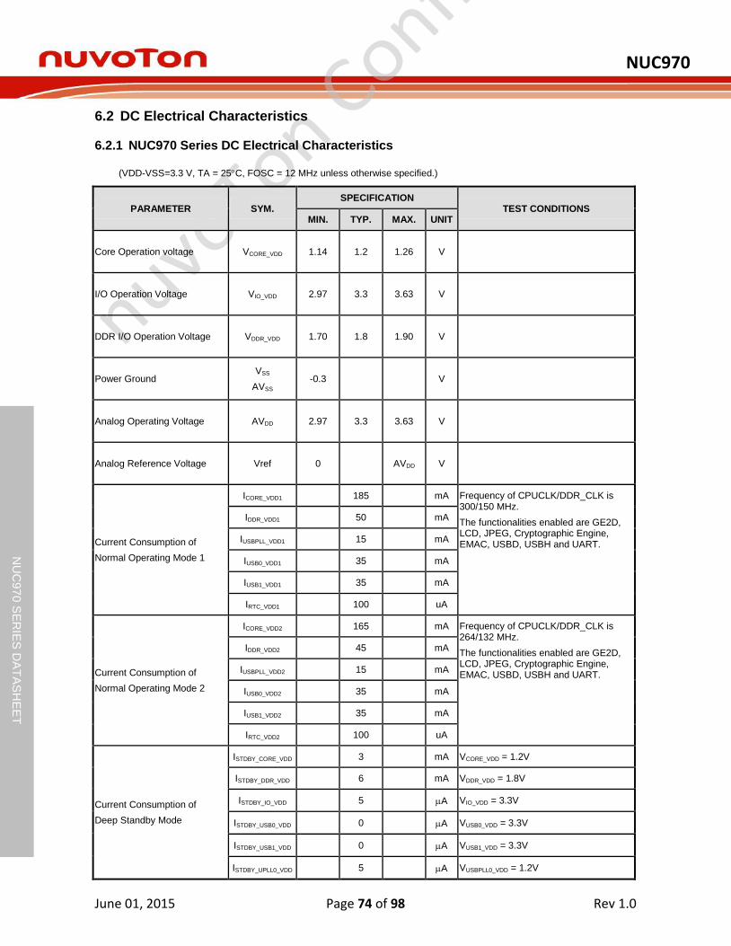
NUC970
June 01, 2015 Page 74 of 98 Rev 1.0
NU
C97
0 S
ER
IES
DA
TA
SH
EE
T
6.2 DC Electrical Characteristics
6.2.1 NUC970 Series DC Electrical Characteristics
(VDD-VSS=3.3 V, TA = 25C, FOSC = 12 MHz unless otherwise specified.)
PARAMETER SYM. SPECIFICATION
TEST CONDITIONS MIN. TYP. MAX. UNIT
Core Operation voltage VCORE_VDD 1.14 1.2 1.26 V
I/O Operation Voltage VIO_VDD 2.97 3.3 3.63 V
DDR I/O Operation Voltage VDDR_VDD 1.70 1.8 1.90 V
Power Ground VSS
AVSS -0.3 V
Analog Operating Voltage AVDD 2.97 3.3 3.63 V
Analog Reference Voltage Vref 0 AVDD V
Current Consumption of
Normal Operating Mode 1
ICORE_VDD1 185 mA Frequency of CPUCLK/DDR_CLK is 300/150 MHz.
The functionalities enabled are GE2D, LCD, JPEG, Cryptographic Engine, EMAC, USBD, USBH and UART.
IDDR_VDD1 50 mA
IUSBPLL_VDD1 15 mA
IUSB0_VDD1 35 mA
IUSB1_VDD1 35 mA
IRTC_VDD1 100 uA
Current Consumption of
Normal Operating Mode 2
ICORE_VDD2 165 mA Frequency of CPUCLK/DDR_CLK is 264/132 MHz.
The functionalities enabled are GE2D, LCD, JPEG, Cryptographic Engine, EMAC, USBD, USBH and UART.
IDDR_VDD2 45 mA
IUSBPLL_VDD2 15 mA
IUSB0_VDD2 35 mA
IUSB1_VDD2 35 mA
IRTC_VDD2 100 uA
Current Consumption of
Deep Standby Mode
ISTDBY_CORE_VDD 3 mA VCORE_VDD = 1.2V
ISTDBY_DDR_VDD 6 mA VDDR_VDD = 1.8V
ISTDBY_IO_VDD 5 A VIO_VDD = 3.3V
ISTDBY_USB0_VDD 0 A VUSB0_VDD = 3.3V
ISTDBY_USB1_VDD 0 A VUSB1_VDD = 3.3V
ISTDBY_UPLL0_VDD 5 A VUSBPLL0_VDD = 1.2V
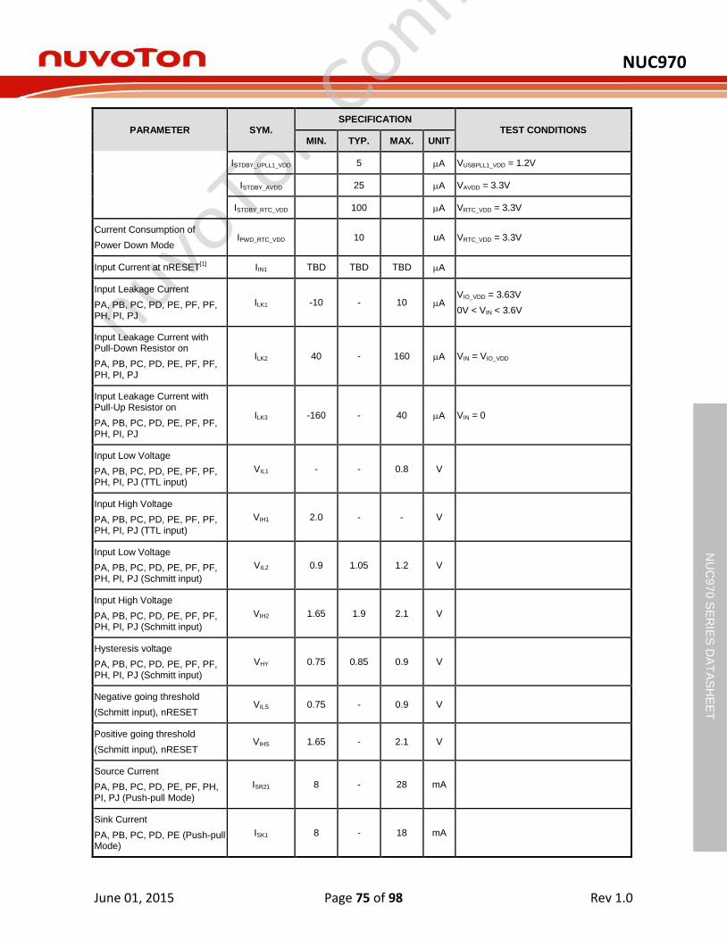
NUC970
June 01, 2015 Page 75 of 98 Rev 1.0
NU
C97
0 S
ER
IES
DA
TA
SH
EE
T
PARAMETER SYM. SPECIFICATION
TEST CONDITIONS MIN. TYP. MAX. UNIT
ISTDBY_UPLL1_VDD 5 A VUSBPLL1_VDD = 1.2V
ISTDBY_AVDD 25 A VAVDD = 3.3V
ISTDBY_RTC_VDD 100 A VRTC_VDD = 3.3V
Current Consumption of
Power Down Mode IPWD_RTC_VDD 10 uA VRTC_VDD = 3.3V
Input Current at nRESET[1]
IIN1 TBD TBD TBD A
Input Leakage Current
PA, PB, PC, PD, PE, PF, PF, PH, PI, PJ
ILK1 -10 - 10 A VIO_VDD = 3.63V
0V < VIN < 3.6V
Input Leakage Current with Pull-Down Resistor on
PA, PB, PC, PD, PE, PF, PF, PH, PI, PJ
ILK2 40 - 160 A VIN = VIO_VDD
Input Leakage Current with Pull-Up Resistor on
PA, PB, PC, PD, PE, PF, PF, PH, PI, PJ
ILK3 -160 - 40 A VIN = 0
Input Low Voltage
PA, PB, PC, PD, PE, PF, PF, PH, PI, PJ (TTL input)
VIL1 - - 0.8 V
Input High Voltage
PA, PB, PC, PD, PE, PF, PF, PH, PI, PJ (TTL input)
VIH1 2.0 - - V
Input Low Voltage
PA, PB, PC, PD, PE, PF, PF, PH, PI, PJ (Schmitt input)
VIL2 0.9 1.05 1.2 V
Input High Voltage
PA, PB, PC, PD, PE, PF, PF, PH, PI, PJ (Schmitt input)
VIH2 1.65 1.9 2.1 V
Hysteresis voltage
PA, PB, PC, PD, PE, PF, PF, PH, PI, PJ (Schmitt input)
VHY 0.75 0.85 0.9 V
Negative going threshold
(Schmitt input), nRESET VILS 0.75 - 0.9 V
Positive going threshold
(Schmitt input), nRESET VIHS 1.65 - 2.1 V
Source Current
PA, PB, PC, PD, PE, PF, PH, PI, PJ (Push-pull Mode)
ISR21 8 - 28 mA
Sink Current
PA, PB, PC, PD, PE (Push-pull Mode)
ISK1 8 - 18 mA

NUC970
June 01, 2015 Page 76 of 98 Rev 1.0
NU
C97
0 S
ER
IES
DA
TA
SH
EE
T
PARAMETER SYM. SPECIFICATION
TEST CONDITIONS MIN. TYP. MAX. UNIT
Input Pull-up Resistance
PA, PB, PC, PD, PE, PF, PF, PH, PI, PJ
RPU 45 53 82 kΩ VIN = 0
Input Pull-down Resistance
PA, PB, PC, PD, PE, PF, PF, PH, PI, PJ
RPD 37 49 91 kΩ VIN = VIO_VDD
Input Pull-up Resistance
nRESET RRST 45 53 85 kΩ
Note:
1. nRESET pin is a Schmitt trigger input.
2. Pins of PA, PB, PC, PD, PE, PF, PG, PH, PI and PJ can source a transition current when they are being externally driven from 1 to 0. In the condition of VDD=3.63 V, the transition current reaches its maximum value when VIN approximates to 1.5 V.

NUC970
June 01, 2015 Page 77 of 98 Rev 1.0
NU
C97
0 S
ER
IES
DA
TA
SH
EE
T
6.3 AC Electrical Characteristics
6.3.1 External 4~24 MHz High Speed Oscillator
Symbol Parameter Min Typ Max Unit Test Condition
tCHCX Clock High Time 20 - - ns -
tCLCX Clock Low Time 20 - - ns -
tCLCH Clock Rise Time - - 10 ns -
tCHCL Clock Fall Time - - 10 ns -
tCHCX
90%
10%
tCLCH
tCHCL
tCLCX
tCLCL
0.3 VDD
0.7 VDD
Note: Duty cycle is 50%.
Figure 66.3-1 External 4~24 MHz High Speed Oscillator Timing Diagram

NUC970
June 01, 2015 Page 78 of 98 Rev 1.0
NU
C97
0 S
ER
IES
DA
TA
SH
EE
T
6.3.2 External 4~24 MHz High Speed Crystal
Symbol Parameter Min. Typ. Max Unit Test Conditions
V XT Operation Voltage 2.97 3.3 3.63 V -
TA Temperature -40 - 85 C -
I XT Operation Current - TBD - mA 12 MHz, VDD = 3.3V
f XT Clock Frequency 4 - 24 MHz -
6.3.2.1 Typical Crystal Application Circuits
Crystal ESR (ohm) C1, C2
4M ~ 8M < 100 20 pf
8M ~ 18M < 50 14 pf
18 MHz ~ 24 MHz < 30 8 pf
XT1_IN
C1 C2
XT1_OUT
4~24 MHz
Crystal
Vss Vss
Figure 6.3-2 Typical HXT Crystal Application Circuit

NUC970
June 01, 2015 Page 79 of 98 Rev 1.0
NU
C97
0 S
ER
IES
DA
TA
SH
EE
T
6.3.3 External 32.768 kHz Low Speed Crystal
Symbol Parameter Min. Typ. Max Unit Test Conditions
VLXT Operation Voltage 2.97 3.3 3.63 V -
TA Temperature -40 - 85 C -
ILXT Operation Current - TBD - mA 32.768 kHz, VDD = 3.3V
fLXT Clock Frequency - 32.768 - kHz -
6.3.3.1 Typical Crystal Application Circuits
Crystal C1 C2
32.768 kHz TBD TBD
X32_IN
C1 C2
X32_OUT
Crystal
Vss Vss
Figure 6.3-3 Typical LXT Crystal Application Circuit

NUC970
June 01, 2015 Page 80 of 98 Rev 1.0
NU
C97
0 S
ER
IES
DA
TA
SH
EE
T
6.3.4 EBI Timing
Symbol Parameter Min Typ Max Unit Test Condition
TtACS Address Setup Time to EBI_nCS
Falling Edge 0 - 7 T CLK -
TtCOS EBI_nCS Setup Time to
EBI_nWE or EBI_nOE Falling Edge
0 - 7 T CLK -
TtACC EBI_nWE or EBI_nOE Active Low
Time 1 - 23 T CLK -
TtCO EBI_nCS old Time from
EBI_nWE or EBI_nOE Rising Edge
0 - 7 T CLK -
TSU_EBI_RD EBI_DATA Read Setup Time to
EBI_nOE Rising Edge 1 - - T CLK -
Note: THCLK is the period of EBI’s operating clock.
EBI_ADDR[9:0]
EBI_nCS[4:0]
EBI_nWE,
EBI_nBE[1:0]
TtACS
TtCOS
TtACC+2
TtCOH
EBI_DATA[15:0
(Write)]Valid Data
EBI_nOE
TtCOS
TtACC+2
TtCOH
EBI_DATA[15:0
(Write)]Valid Data
TSU_EBI_RD
Figure 6.3-4 External Bus Interface Timing Diagram

NUC970
June 01, 2015 Page 81 of 98 Rev 1.0
NU
C97
0 S
ER
IES
DA
TA
SH
EE
T
6.3.5 I2C Interface Timing
Symbol Parameter 100K 400K
Unit Test Condition Min Max Min Max
TLOW I2C_SCL Low Period 4.7 - 1.2 - us -
T IG I2C_SCL igh Period 4 - 0.6 - us -
TSU_STA Repeated START Condition
Setup Time 4.7 - 1.2 - us -
T D_STA START Condition old Time 4 - 0.6 - us -
TSU_STO STOP Condition Setup Time 4 - 0.6 - us -
TBUF Bus Free Time 4.7 - 1.2 - us -
TSU_DAT Data Setup Time 2 - 0.3 - us -
T D_DAT Data old Time 0 4.2 0 0.8 us -
TR I2C_SCL/I2C_SDA Rise Time - 1000 20+0.1Cb 300 ns -
TF I2C_SCL/I2C_SDA Fall Time - 300 - 300 ns -
Cb Capacitive Load for Each Bus
Line - 400 - 400 pF -
TBUF
STOP
I2C_SDA
I2C_SCL
START
THD_STA
TLOW
THD_DAT
THIGH
TF
TSU_DAT
Repeated
START
TSU_STA TSU_STO
STOP
TR
Figure 6.3-5 I2C Interface Timing Diagram

NUC970
June 01, 2015 Page 82 of 98 Rev 1.0
NU
C97
0 S
ER
IES
DA
TA
SH
EE
T
6.3.6 SPI Interface Timing
Symbol Parameter Min Typ Max Unit Test Condition
TP_SPI_CLK SPI_CLK Period 56 - - ns -
T _SPI_CLK SPI_CLK igh Time 28 - - ns -
TL_SPI_CLK SPI_CLK Low Time 28 - - ns -
TSU_SPI_DI SPI_DI or SPI_DATA[3:0] Setup Time to SPI_CLK Active Edge
11 - - ns -
T D_SPI_DI SPI_DI or SPI_DATA[3:0] old Time from SPI_CLK Active Edge
1 - - ns -
TDLY_SPI_DO SPI_CLK Active Edge to Valid
SPI_DO or SPI_DATA[3:0] Delay - - 4 ns -
T D_SPI_DO SPI_DO or SPI_DATA[3:0] old Time from SPI_CLK Active Edge
0.2 ns
SPIx_CLK
SPIx_DI
SPIx_DATA[3:0]
TSU_SPI_DI
THD_SPI_DI
TP_SPI_CLK
TL_SPI_CLK TH_SPI_CLK
TDLY_SPI_DO THD_SPI_DO
SPIx_DO
SPIx_DATA[3:0]
TL_SPI_CLK
TH_SPI_CLK
Figure 6.3-6 SPI Interface Timing Diagram

NUC970
June 01, 2015 Page 83 of 98 Rev 1.0
NU
C97
0 S
ER
IES
DA
TA
SH
EE
T
6.3.7 I2S Interface Timing
Symbol Parameter Min Typ Max Unit Test Condition
TP_I2S_BITCLK I2S_BITCLK Period 50 - - ns -
T _I2S_BITCLK I2S_BITCLK igh Time 25 - - ns -
TL_I2S_BITCLK I2S_BITCLK Low Time 25 - - ns -
TDLY_I2S_DO I2S_BITCLK Rising to Valid
I2S_WS or I2S_DATAO Delay - - 6 ns -
T D_I2S_DO I2S_WS or I2S_DATAO old Time
from I2S_BITCLK Rising 1 - - ns
TSU_I2S_DI I2S_DATAI Setup Time to
I2S_BITCLK Rising 5 - - ns -
T D_I2S_DI I2S_DATAI old Time from
I2S_BITCLK Rising 3 - - ns -
I2S_BITCLK
I2S_DATAI
TSU_I2S_DI
THD_I2S_DI
TP_I2S_BITCLK
TL_I2S_BITCLK TH_I2S_BITCLK
TDLY_I2S_DO THD_I2S_DO
I2S_WS
I2S_DATAO
Figure 6.3-7 I2S Interface Timing Diagram
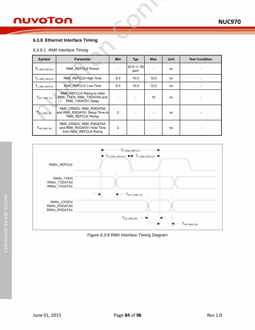
NUC970
June 01, 2015 Page 84 of 98 Rev 1.0
NU
C97
0 S
ER
IES
DA
TA
SH
EE
T
6.3.8 Ethernet Interface Timing
6.3.8.1 RMII Interface Timing
Symbol Parameter Min Typ Max Unit Test Condition
TP_R II_REFCLK R II_REFCLK Period - 20.0 +/- 50
ppm - ns -
T _R II_REFCLK R II_REFCLK igh Time 8.0 10.0 12.0 ns -
TL_R II_REFCLK RMII_REFCLK Low Time 8.0 10.0 12.0 ns -
TDLY_R II_TX R II_REFCLK Rising to Valid
R II_TXEN, R II_TXDATA0 and R II_TXDATA1 Delay
- - 10 ns -
TSU_R II_RX R II_CRSDV, R II_RXDATA0
and R II_RXDATA1 Setup Time to R II_REFCLK Rising
5 - - ns -
T D_R II_RX R II_CRSDV, R II_RXDATA0 and R II_RXDATA1 old Time from R II_REFCLK Rising
2 - - ns -
RMIIx_REFCLK
TP_RMII_REFCLK
TH_RMII_REFCLK TL_RMII_REFCLK
RMIIx_TXEN
RMIIx_TXDATA0
RMIIx_TXDATA1
TDLY_RMII_TX
RMIIx_CRSDV
RMIIx_RXDATA0
RMIIx_RXDATA1
TSU_RMII_RX
THD_RMII_RX
Figure 6.3-8 RMII Interface Timing Diagram

NUC970
June 01, 2015 Page 85 of 98 Rev 1.0
NU
C97
0 S
ER
IES
DA
TA
SH
EE
T
6.3.8.2 Ethernet PHY Management Interface Timing
Symbol Parameter Min Typ Max Unit Test Condition
TP_R II_ DC R II_ DC Period 400 - - ns -
T _R II_ DC R II_ DC igh Time 200 - - ns -
TL_R II_ DC RMII_MDC Low Time 200 - - ns -
TDLY_R II_ DIOWR R II_ DC Falling to Valid
R II_ DIO Delay - - 10 ns -
TSU_R II_ DIORD R II_ DIO Setup Time to
R II_ DC Rising 10 - - ns -
T D_R II_ DIORD R II_ DIO old Time from
R II_ DC Rising 10 - - ns -
RMIIx_MDC
TP_RMII_MDC
TH_RMII_MDC TL_RMII_MDC
RMIIx_MDIO
(Write)
TDLY_RMII_MDIOWR
RMIIx_MDIO
(Read)
TSU_RMII_MDIORD
THD_RMII_MDIORD
Figure 6.3-9 Ethernet PHY Management Interface Timing Diagram

NUC970
June 01, 2015 Page 86 of 98 Rev 1.0
NU
C97
0 S
ER
IES
DA
TA
SH
EE
T
6.3.9 NAND Interface Timing
Symbol Parameter Min Typ Max Unit Test Condition
T _NAND_nWE NAND_nWE igh Time - 151 - ns -
TL_NAND_nWE NAND_nWE Low Time - 452 - ns -
TDLY_DATA_OUT NAND_nWE Falling to Valid
NAND_DATA Delay - 15
3-
ns -
T D_DATA_OUT NAND_DATA old Time from
NAND_nWE Rising 7.5
3 - - Ns -
TSU_DATA_IN NAND_DATA Setup Time to
NAND_nRE Rising 15
3 - - ns -
T D_DATA_IN NAND_DATA old Time from
NAND_nRE Rising 7.5
3 - - ns -
Note 1: NAND controller operating clock is 132 MHz and HI_WID (FMI_NANDTMCTL[15:8]) is 0x1.
Note 2: NAND controller operating clock is 132 MHz and LO_WID (FMI_NANDTMCTL[7:0]) is 0x5.
Note 2: NAND controller operating clock is 132 MHz
NAND_nCS0
NAND_nCS1
NAND_ALE
NAND_CLE
NAND_nWE
NAND_nRE
NAND_DATA[7:0]
(Write)
NAND_DATA[7:0]
(Read)
TH_NAND_nWETL_NAND_nWE
TDLY_DATA_OUT
THD_DATA_OUT
THD_DATA_IN
TSU_DATA_IN
Figure 6.3-10 NAND Interface Timing Diagram

NUC970
June 01, 2015 Page 87 of 98 Rev 1.0
NU
C97
0 S
ER
IES
DA
TA
SH
EE
T
6.3.10 SD Interface Timing
6.3.10.1 Default Mode Timing
Symbol Parameter Min Typ Max Unit Test Condition
TP_SD_CLK SD_CLK Period
(Data Transfer ode) 40 - - ns -
TP_SD_CLK_ID SD_CLK Period
(Identification ode) 2,500 - - ns
T _SD_CLK SD_CLK igh Time - 20 - ns -
TL_SD_CLK SD_CLK Low Time - 20 - ns -
TSU_SD_IN SD_DATA Setup Time to
SD_CLK Rising 5 - - ns -
T D_SD_IN SD_DATA old Time from
SD_CLK Rising 5 - - ns -
TDLY_SD_OUT SD_CLK Falling to
Valid SD_DATA Delay - - 14 ns -
SDx_CLK
SDx_CMD
SDx_DATA[3:0]
(Input Mode)
TSU_SD_IN
THD_SD_IN
TP_SD_CLK
TL_SD_CLK TH_SD_CLK
SDx_CMD
SDx_DATA[3:0]
(Output Mode)
TDLY_SD_OUT
Figure 6.3-11 SD Interface Default Mode Timing Diagram

NUC970
June 01, 2015 Page 88 of 98 Rev 1.0
NU
C97
0 S
ER
IES
DA
TA
SH
EE
T
6.3.10.2 High-Speed Mode Timing
Symbol Parameter Min Typ Max Unit Test Condition
TP_SD_CLK SD_CLK Period 20 - - ns -
T _SD_CLK SD_CLK igh Time 7 - - ns -
TL_SD_CLK SD_CLK Low Time 7 - - ns -
TSU_SD_IN SD_DATA Setup Time to
SD_CLK Rising 6 - - ns -
T D_SD_IN SD_DATA old Time from
SD_CLK Rising 2 - - ns -
TDLY_SD_OUT SD_CLK Falling to
Valid SD_DATA Delay - - 14 ns -
T D_SD_OUT SD_DATA old Time from
SD_CLK Rising 2.5 - - ns -
SDx_CLK
SDx_CMD
SDx_DATA[3:0]
(Input Mode)
TSU_SD_IN
THD_SD_IN
TP_SD_CLK
TL_SD_CLK TH_SD_CLK
THD_SD_OUT
SDx_CMD
SDx_DATA[3:0]
(Output Mode)
TDLY_SD_OUT
Figure 6.3-12 SD Interface High-Speed Mode Timing Diagram
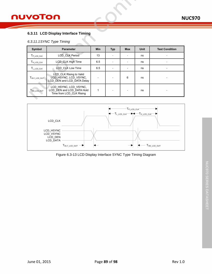
NUC970
June 01, 2015 Page 89 of 98 Rev 1.0
NU
C97
0 S
ER
IES
DA
TA
SH
EE
T
6.3.11 LCD Display Interface Timing
6.3.11.1 SYNC Type Timing
Symbol Parameter Min Typ Max Unit Test Condition
TP_LCD_CLK LCD_CLK Period 13 - - ns -
T _LCD_CLK LCD_CLK igh Time 6.5 - - ns -
TL_LCD_CLK LCD_CLK Low Time 6.5 - - ns -
TDLY_LCD_OUT LCD_CLK Rising to Valid
LCD_ SYNC, LCD_VSYNC, LCD_DEN and LCD_DATA Delay
- - 6 ns -
T D_LCD_OUT LCD_ SYNC, LCD_VSYNC,
LCD_DEN and LCD_DATA old Time from LCD_CLK Rising
1 - - ns -
LCD_CLK
LCD_HSYNC
LCD_VSYNC
LCD_DEN
LCD_DATA
TDLY_LCD_OUT THD_LCD_OUT
TP_LCD_CLK
TL_LCD_CLK TH_LCD_CLK
Figure 6.3-13 LCD Display Interface SYNC Type Timing Diagram
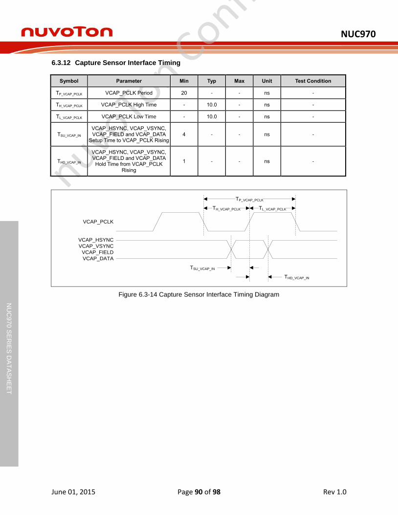
NUC970
June 01, 2015 Page 90 of 98 Rev 1.0
NU
C97
0 S
ER
IES
DA
TA
SH
EE
T
6.3.12 Capture Sensor Interface Timing
Symbol Parameter Min Typ Max Unit Test Condition
TP_VCAP_PCLK VCAP_PCLK Period 20 - - ns -
T _VCAP_PCLK VCAP_PCLK igh Time - 10.0 - ns -
TL_VCAP_PCLK VCAP_PCLK Low Time - 10.0 - ns -
TSU_VCAP_IN VCAP_ SYNC, VCAP_VSYNC, VCAP_FIELD and VCAP_DATA
Setup Time to VCAP_PCLK Rising 4 - - ns -
T D_VCAP_IN
VCAP_ SYNC, VCAP_VSYNC, VCAP_FIELD and VCAP_DATA old Time from VCAP_PCLK
Rising
1 - - ns -
VCAP_PCLK
VCAP_HSYNC
VCAP_VSYNC
VCAP_FIELD
VCAP_DATA
TSU_VCAP_IN
THD_VCAP_IN
TP_VCAP_PCLK
TH_VCAP_PCLK TL_VCAP_PCLK
Figure 6.3-14 Capture Sensor Interface Timing Diagram

NUC970
June 01, 2015 Page 91 of 98 Rev 1.0
NU
C97
0 S
ER
IES
DA
TA
SH
EE
T
6.4 Analog Characteristics
6.4.1 12-bit SARADC
Symbol Parameter Min. Typ. Max. Unit Test Conditions
- Resolution - 12 - Bit
DNL Differential Nonlinearity Error - ±1 - LSB VREF is external AVREF pin
INL Integral Nonlinearity Error - -1.2 - LSB VREF is external AVREF pin
EO Offset Error - +3.7 - LSB VREF is external AVREF pin
EG Gain Error (Transfer Gain) - -6.6 - LSB VREF is external AVREF pin
EA Absolute Error - 4.2 - LSB VREF is external AVREF pin
- Monotonic Guaranteed
FADC ADC Clock Frequency - - 16 MHz
TCAL Calibration Time - 3 - Clock
TS Sample Time - 17 - Clock
TADC Conversion Time - 20 Clock
FS Sample Rate - - 800[1]
k SPS
VAVDD Supply Voltage 2.7 3.3 3.6 V
IDDA1 Supply Current (Avg.) - 1.2
mA ADC1 channel high speed mode
IDDA2 Supply Current (Avg.) - 1.0
mA ADC1 channel low speed mode
IDDA3 Supply Current (Avg.) - 0.4 mA
ILK Leakage Current - 0.1 - uA
VREF Reference Voltage 2 - VAVDD V
VIN Analog Input Voltage 0 - VREF V
RIN Analog Input Impedance - - 2 MΩ
CIN Capacitance - 25.6 pF
Note:
1. ADC1 channel supports sample rate higher than 200 kSPS. Other ADC channels support sampel rate up to 200 kSPS.
NUC970
June 01, 2015 Page 92 of 98 Rev 1.0
NU
C97
0 S
ER
IES
DA
TA
SH
EE
T
6.4.2 Low Voltage Detection (LVD) and Low Voltage Reset (LVR)
Symbol Parameter Min. Typ. Max Unit Test Conditions
VDD Operation Voltage 2.0 3.3 3.63 V -
IDD Operating Current 21 uA -
ILK Quiescent Current - 0.1 0.5 uA LVR_EN (SYS_LVRDCR[0]) = 0,
LVD_EN (SYS_LVRDCR[8]) = 0
TA Temperature -40 - 85 C -
VT _LVD LVD Threshold Voltage 2.295 2.55 2.805 V LVD_SEL (SYS_LVRDCR[9]) = 0
2.475 2.75 3.025 V LVD_SEL (SYS_LVRDCR[9]) = 1
VT _LVR LVR Threshold Voltage 2.115 2.35 2.585 V -
V Y_LVD LVD Hysteresis 0.045 0.05 0.055 V LVD_SEL (SYS_LVRDCR[9]) = 0
0.045 0.05 0.055 V LVD_SEL (SYS_LVRDCR[9]) = 1
V Y_LVR LVR Hysteresis 0.045 0.05 0.055 V -

NUC970
June 01, 2015 Page 93 of 98 Rev 1.0
NU
C97
0 S
ER
IES
DA
TA
SH
EE
T
6.4.3 3.3V Power-On Reset (POR33)
Symbol Parameter Min Typ Max Unit Test Condition
TA Temperature -40 25 125 C -
VPOR Reset Voltage - 1.83 - V AVDD rising from 0V to
3.3V
IPOR33 Quiescent current - 5 - nA Vin > reset voltage
6.4.4 1.2V Power-On Reset (POR12)
Symbol Parameter Min Typ Max Unit Test Condition
TA Temperature -40 25 125 C -
VPOR Reset Voltage - 0.76 - V CORE_VDD rising from
0V to 1.2V
IPOR12 Quiescent current - 10 - nA Vin > reset voltage
6.4.5 USB 2.0 PHY
6.4.5.1 Low/Full-Speed DC Electrical Specifications
Symbol Parameter Min Typ Max Unit Test Condition
VOL Output Low (Driven) - - 0.3 V 1.5K RPU on DP to 3.6v
VO Output igh (Driven) 2.8 - - V 15K RPD on DP, D to
GND
VDI Differential Input Sensitivity 0.2 - - V |VUSB0_DP–VUSB0_D |
VC Differential Common- ode Range 0.8 - 2.5 V
VIL Single-Ended Input Low - - 0.8 V -
VI Single-Ended Input igh 2.0 - - V -
RPU Pull-Up Resistor 1.35 1.5 1.65 kΩ
RPD_DP D+ Pull-Down Resistor 13.5 15 16.5 kΩ
RPD_D D- Pull-Down Resistor 13.5 15 16.5 kΩ
ZDRV Driver Output Resistance 28 - 44 Ω Steady state drive[1]
Note:
1. Driver output resistance doesn’t include series resistor resistance.
6.4.5.2 High-Speed DC Electrical Specifications
Symbol Parameter Min Typ Max Unit Test Condition
V SDI igh Speed Differential Input
Signal Level 150 - - mV |VUSB0_DP–VUSB0_D |

NUC970
June 01, 2015 Page 94 of 98 Rev 1.0
NU
C97
0 S
ER
IES
DA
TA
SH
EE
T
V SQ igh Speed Squelch Detection
Threshold 100 125 150 mV |VUSB0_DP–VUSB0_D |
V SC igh Speed Common ode
Voltage Range -50 - 500 mV
V SO igh Speed Data Signaling igh 300 400 440 mV
V SOL igh Speed Data Signaling Low -10 0 10 mV
VC IRPJ Chirp J Level 700 - 1100 mV
VC IRPK Chirp K Level -900 - -500 mV
R SDRV igh Speed Driver Output
Resistance 40.5 45 49.5 Ω
6.4.5.3 USB Low-Speed Driver AC Electrical Characteristics
Symbol Parameter Min Typ Max Unit Test Condition
TLRISE Rise Time 75 - 300 ns CL=200pF, 10% to 90% of
|VO -VOL|
TLFALL Fall Time 75 - 300 ns CL=200pF, 10% to 90% of
|VO -VOL|
VLCR Crossover Voltage 1.3 - 2.0 V Excluding the first
transition from idle state
6.4.5.4 USB Full-Speed Driver AC Electrical Characteristics
Symbol Parameter Min Typ Max Unit Test Condition
VFRISE Rise Time 4 - 20 ns CL=50pF, 10% to 90% of
|VO -VOL|
VFFALL Fall Time 4 - 20 ns CL=50pF, 10% to 90% of
|VO -VOL|
VFCR Crossover Voltage 1.3 - 2.0 V Excluding the first
transition from idle state
6.4.5.5 USB High-Speed Driver AC Electrical Characteristics
Symbol Parameter Min Typ Max Unit Test Condition
V RISE igh Speed Driver Rise Time 500 - 900 ps CL<10pF
V FALL igh Speed Driver Fall Time 500 - 900 ps CL<10pF

NUC970
June 01, 2015 Page 95 of 98 Rev 1.0
NU
C97
0 S
ER
IES
DA
TA
SH
EE
T
7 PACKAGE DIMENSIONS
7.1 216L LQFP (24x24x1.4mm footprint 2.0mm)
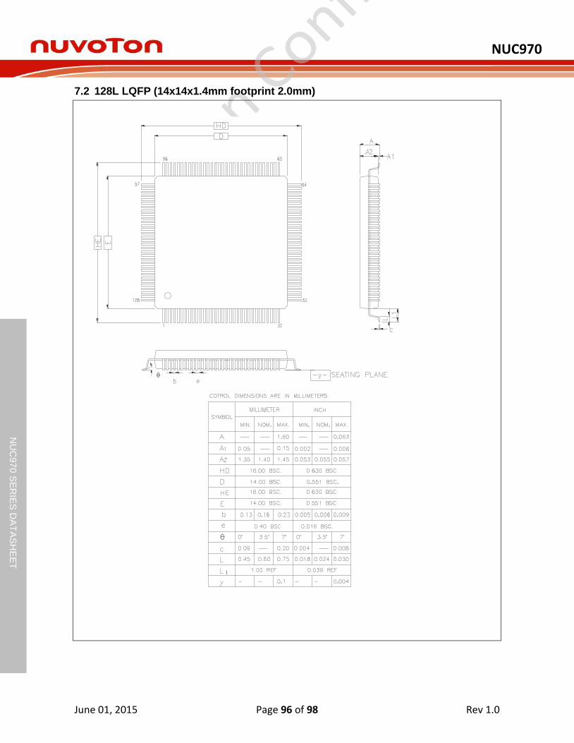
NUC970
June 01, 2015 Page 96 of 98 Rev 1.0
NU
C97
0 S
ER
IES
DA
TA
SH
EE
T
7.2 128L LQFP (14x14x1.4mm footprint 2.0mm)

NUC970
June 01, 2015 Page 97 of 98 Rev 1.0
NU
C97
0 S
ER
IES
DA
TA
SH
EE
T
8 REVISION HISTORY
Date Revision Description
2015.05.12 1.0 1. Preliminary version.

NUC970
June 01, 2015 Page 98 of 98 Rev 1.0
NU
C97
0 S
ER
IES
DA
TA
SH
EE
T
Important Notice
Nuvoton Products are neither intended nor warranted for usage in systems or equipment, any malfunction or failure of which may cause loss of human life, bodily injury or severe property damage. Such applications are deemed, “Insecure Usage”.
Insecure usage includes, but is not limited to: equipment for surgical implementation, atomic energy control instruments, airplane or spaceship instruments, the control or operation of dynamic, brake or safety systems designed for vehicular use, traffic signal instruments, all types of safety devices, and other applications intended to support or sustain life.
All Insecure Usage shall be made at customer’s risk, and in the event that third parties lay claims to Nuvoton as a result of customer’s Insecure Usage, customer shall indemnify the damages and liabilities thus incurred by Nuvoton.