number: 002-12878 rev. *c page 2 of 151 s25fl064l performance summary maximum read rates sdr command...
TRANSCRIPT

Cypress Semiconductor Corporation • 198 Champion Court • San Jose, CA 95134-1709 • 408-943-2600Document Number: 002-12878 Rev. *D Revised April 04, 2018
S25FL064L
64-Mbit (8-Mbyte)3.0 V FL-L SPI Flash Memory
General DescriptionThe Cypress FL-L Family devices are Flash Nonvolatile Memory products using:
Floating Gate technology
65-nm process lithography
The FL-L family connects to a host system via a Serial Peripheral Interface (SPI). Traditional SPI single bit serial input and output (Single I/O or SIO) is supported as well as optional two bit (Dual I/O or DIO) and four bit wide Quad I/O (QIO), and Quad Peripheral Interface (QPI) commands. In addition, there are Double Data Rate (DDR) read commands for QIO and QPI that transfer address and read data on both edges of the clock.
The architecture features a Page Programming Buffer that allows up to 256-bytes to be programmed in one operation and provides individual 4 KB sector, 32 KB half block sector, 64 KB block sector, or entire chip erase.
By using FL-L family devices at the higher clock rates supported, with Quad commands, the instruction read transfer rate can match or exceed traditional parallel interface, asynchronous, NOR Flash memories, while reducing signal count dramatically.
The FL-L family products offer high densities coupled with the flexibility and fast performance required by a variety of mobile or embedded applications. Provides an ideal storage solution for systems with limited space, signal connections, and power. These memories offer flexibility and performance well beyond ordinary serial flash devices. They are ideal for code shadowing to RAM, executing code directly (XIP), and storing re-programmable data.
Features Serial Peripheral Interface (SPI) with Multi-I/O
– Clock polarity and phase modes 0 and 3– Double Data Rate (DDR) option– Quad peripheral interface (QPI) option– Extended addressing: 24- or 32-bit address options– Serial command subset and footprint compatible with S25FL-A,
S25FL1-K, S25FL-P, S25FL-S, and S25FS-S SPI families– Multi I/O command subset and footprint compatible with S25FL-P,
S25FL-S and S25FS-S SPI families Read
– Commands: Normal, Fast, Dual I/O, Quad I/O, DualO, QuadO, DDR Quad I/O
– Modes: Burst wrap, Continuous (XIP), QPI– Serial flash discoverable parameters (SFDP) for configuration
information Program Architecture
– 256-Bytes page programming buffer– Program suspend and resume
Erase Architecture– Uniform 4 KB sector erase– Uniform 32 KB half block erase– Uniform 64 KB block erase – Chip erase– Erase suspend and resume
100,000 Program-Erase Cycles, minimum 20 Year Data Retention, minimum Security Features
– Status and configuration Register protection
– Four security regions of 256-bytes each outside the main Flash array
– Legacy block protection: Block range– Individual and region protection
– Individual block lock: Volatile individual sector/block – Pointer region: Non-volatile sector/block range– Power supply Lock-down, password, or permanent protection
of security regions 2 and 3 and pointer region Technology
– 65-nm Floating Gate technology Single Supply Voltage with CMOS I/O
– 2.7 V to 3.6 V Temperature Range / Grade
– Industrial (–40°C to +85°C)– Industrial Plus (–40°C to +105°C)– Automotive, AEC-Q100 Grade 3 (–40°C to +85°C)– Automotive, AEC-Q100 Grade 2 (–40°C to +105°C)– Automotive, AEC-Q100 Grade 1 (–40°C to +125°C)
Packages (All Pb-free)– 8-lead SOIC 208 mil (SOC008)– 16-lead SOIC 300 mil (SO3016)– USON 4 4 mm (UNF008)– WSON 5 x 6 mm (WND008)– BGA-24 6 8 mm
– 5 5 ball (FAB024) footprint– 4 6 ball (FAC024) footprint
– Known good die and known tested die

Document Number: 002-12878 Rev. *D Page 2 of 152
S25FL064L
Performance SummaryMaximum Read Rates SDR
Command Clock Rate (MHz) MBps
Read 50 6.25
Fast Read 108 13.5
Dual Read 108 27
Quad Read 108 54
Maximum Read Rates DDR
Command Clock Rate (MHz) MBps
DDR Quad Read 54 54
Typical Program and Erase Rates
Operation KBytes/s
Page Programming 569
4 KBytes Sector Erase 61
32 KBytes Half Block Erase 106
64 KBytes Block Erase 142
Typical Current Consumption
Operation Typical Current Unit
Read 50 MHz 10 mA
Fast Read 5MHz 10 mA
Fast Read 10 MHz 10 mA
Fast Read 20 MHz 10 mA
Fast Read 50 MHz 15 mA
Fast Read 108 MHz 25 mA
Quad I/O / QPI Read 108 MHz 25 mA
Quad I/O / QPI DDR Read 33MHz 15 mA
Quad I/O / QPI DDR Read 54MHz 30 mA
Program 40 mA
Erase 40 mA
Standby SPI 20 µA
Standby QPI 60 µA
Deep Power Down 2 µA

Document Number: 002-12878 Rev. *D Page 3 of 152
S25FL064L
Contents1. Product Overview ........................................................ 41.1 Migration Notes.............................................................. 4
2. Connection Diagrams.................................................. 62.1 SOIC 16-Lead................................................................ 62.2 8 Connector Packages................................................... 62.3 BGA Ball Footprint ......................................................... 82.4 Special Handling Instructions for FBGA Packages........ 8
3. Signal Descriptions ..................................................... 93.1 Input/Output Summary................................................... 93.2 Multiple Input / Output (MIO)........................................ 103.3 Serial Clock (SCK) ....................................................... 103.4 Chip Select (CS#) ........................................................ 103.5 Serial Input (SI) / IO0 ................................................... 103.6 Serial Output (SO) / IO1............................................... 103.7 Write Protect (WP#) / IO2 ............................................ 103.8 IO3 / RESET# .............................................................. 113.9 RESET#....................................................................... 113.10 Voltage Supply (VCC).................................................. 113.11 Supply and Signal Ground (VSS) ................................. 113.12 Not Connected (NC) .................................................... 113.13 Reserved for Future Use (RFU)................................... 123.14 Do Not Use (DNU) ....................................................... 12
4. Block Diagram............................................................ 134.1 System Block Diagrams............................................... 13
5. Signal Protocols......................................................... 165.1 SPI Clock Modes ......................................................... 165.2 Command Protocol ...................................................... 175.3 Interface States............................................................ 225.4 Data Protection ............................................................ 26
6. Address Space Maps................................................. 276.1 Overview ...................................................................... 276.2 Flash Memory Array..................................................... 276.3 ID Address Space ........................................................ 276.4 JEDEC JESD216 Serial Flash Discoverable Parameters
(SFDP) Space.............................................................. 286.5 Security Regions Address Space ................................ 286.6 Registers...................................................................... 28
7. Data Protection .......................................................... 457.1 Security Regions.......................................................... 457.2 Deep Power Down....................................................... 457.3 Write Enable Commands ............................................. 467.4 Write Protect Signal ..................................................... 467.5 Status Register Protect (SRP1, SRP0)........................ 467.6 Array Protection ........................................................... 487.7 Individual and Region Protection ................................. 53
8. Commands ................................................................. 588.1 Command Set Summary.............................................. 588.2 Identification Commands ............................................. 648.3 Register Access Commands........................................ 678.4 Read Memory Array Commands ................................. 808.5 Program Flash Array Commands ................................ 89
8.6 Erase Flash Array Commands...................................... 918.7 Security Regions Array Commands.............................. 978.8 Individual Block Lock Commands................................. 998.9 Pointer Region Command........................................... 1038.10 Individual and Region Protection
(IRP) Commands ........................................................ 1048.11 Reset Commands ....................................................... 1098.12 Deep Power Down Commands................................... 110
9. Data Integrity ............................................................. 1139.1 Erase Endurance ........................................................ 1139.2 Data Retention............................................................ 113
10. Software Interface Reference .................................. 11410.1 JEDEC JESD216B Serial Flash
Discoverable Parameters............................................ 11410.2 Device ID Address Map .............................................. 12210.3 Initial Delivery State .................................................... 122
11. Electrical Specifications........................................... 12311.1 Absolute Maximum Ratings ........................................ 12311.2 Latchup Characteristics .............................................. 12311.3 Thermal Resistance.................................................... 12311.4 Operating Ranges....................................................... 12311.5 Power-Up and Power-Down ....................................... 12411.6 DC Characteristics ...................................................... 127
12. Timing Specifications............................................... 13012.1 Key to Switching Waveforms ...................................... 13012.2 AC Test Conditions..................................................... 13012.3 Reset .......................................................................... 13112.4 SDR AC Characteristics.............................................. 13412.5 DDR AC Characteristics ............................................. 13712.6 Embedded Algorithm Performance Tables................. 139
13. Ordering Information ................................................ 140
14. Physical Diagrams .................................................... 14214.1 SOIC 8-Lead, 208 mil Body Width (SOC008)............. 14214.2 SOIC 16-Lead, 300 mil Body Width (SO3016) ........... 14314.3 USON 4 x 4 mm (UNF008)......................................... 14414.4 WSON 5x 6mm (WND008)......................................... 14514.5 Ball Grid Array, 24-ball 6 x 8 mm (FAB024)................ 14614.6 Ball Grid Array, 24-ball 6 x 8 mm (FAC024) ............... 147
15. Other Resources ....................................................... 14815.1 Glossary...................................................................... 14815.2 Link to Cypress Flash Roadmap................................. 14915.3 Link to Software .......................................................... 14915.4 Link to Application Notes ............................................ 149
16. Document History ..................................................... 150Sales, Solutions, and Legal Information ........................ 152
Worldwide Sales and Design Support ......................... 152Products ...................................................................... 152PSoC® Solutions ........................................................ 152Cypress Developer Community ................................... 152Technical Support ....................................................... 152

Document Number: 002-12878 Rev. *D Page 4 of 152
S25FL064L
1. Product Overview
1.1 Migration Notes
1.1.1 Features ComparisonThe FL064L family is command subset and footprint compatible with prior generation FL-S, FL1-K and FL-P families.
Note:1. Refer to individual data sheets for further details
Table 1. Cypress SPI Families Comparison
Parameter FL-L FL-L FL-S FL1-K FL-P
Technology Node 65nm 65nm 65nm 90nm 90nm
Architecture Floating Gate Floating Gate MirrorBit® Eclipse™ Floating Gate MirrorBit®
Release Date In Production In Production In Production In Production In Production
Density 64Mb 256Mb 128Mb - 1Gb 16Mb - 64Mb 32Mb - 256Mb
Bus Width x1, x2, x4 x1, x2, x4 x1, x2, x4 x1, x2, x4 x1, x2, x4
Supply Voltage 2.7 V - 3.6 V 2.7 V - 3.6 V2.7 V - 3.6 V / 1.65 V - 3.6 V
VIO 2.7 V - 3.6 V 2.7 V - 3.6 V
Normal Read Speed 6MB/s (50MHz) 6MB/s (50MHz) 6MB/s (50MHz) 6MB/s (50MHz) 5MB/s (40MHz)
Fast Read Speed 13MB/s (108MHz) 16.5MB/s (133MHz) 17MB/s (133MHz) 13MB/s (108MHz) 13MB/s (104MHz)
Dual Read Speed 26MB/s (108MHz) 33MB/s (133MHz) 26MB/s (104MHz) 26MB/s (108MHz) 20MB/s (80MHz)
Quad Read Speed 52MB/s (108MHz) 66MB/s (133MHz) 52MB/s (104MHz) 52MB/s (108MHz) 40MB/s (80MHz)
Quad Read Speed (DDR) 54MB/s (54MHz) 66MB/s (66MHz) 80MB/s (80MHz)
Program Buffer Size 256B 256B 256B / 512B 256B 256B
Erase Sector/Block Size 4KB / 32KB / 64KB 4KB / 32KB / 64KB 64KB / 256KB 4KB / 64KB 64KB / 256KB
Parameter Sector Size - - 4KB (option) 4KB
Sector / Block Erase Rate (typ.)
61 KB/s (4KB)
106 KB/s (32KB
142KB/s (64KB)
80 KB/s (4KB)
168 KB/s (32KB
237KB/s (64KB)
500 KB/s80 KB/s (4KB)
128 KB/s (64KB)130 KB/s
Page Programming Rate (typ.) 569 KB/s (256B) 854KB/s (256B)1.2 MB/s (256B)1.5 MB/s (512B)
365 KB/s 170 KB/s
Security Region / OTP 1024B 1024B 1024B 768B (3 256B) 506B
Individual and Region Protection or Advanced Sector Protection
Yes Yes Yes Yes No
Erase Suspend/Resume Yes Yes Yes Yes No
Program Suspend/Resume Yes Yes Yes Yes No
Operating Temperature
–40°C to +85°C
–40°C to +105°C
–40°C to +125°C
–40°C to +85°C
–40°C to +105°C
–40°C to +125°C
–40°C to +85°C
–40°C to +105°C
–40°C to +85°C
–40°C to +105°C
–40°C to +125°C
–40°C to +85°C
–40°C to +105°C

Document Number: 002-12878 Rev. *D Page 5 of 152
S25FL064L
1.1.2 Known Differences from Prior Generations
1.1.2.1 Error ReportingFL-K, FL1-K and FL-P memories either do not have error status bits or do not set them if program or erase is attempted on a protected sector. This product family does have error reporting status bits for program and erase operations. These can be set when there is an internal failure to program or erase, or when there is an attempt to program or erase a protected sector. In these cases the program or erase operation did not complete as requested by the command. The P_ERR or E_ERR bits and the WIP bit will be set to and remain 1 in SR1V. The clear status register command must be sent to clear the errors and return the device to standby state.
1.1.2.2 Status Register Protect 1 BitThe Configuration Register 1 SRP1 Bit CR1V[0], locks the state of the Legacy Block Protection bits (SR1NV[5:2] & SR1V[5:2]), CMP_NV (CR1NV[6]) and TBPROT_NV bit (SR1NV[6]), as Freeze did in prior generations. In the FS-S and FL-S families the Freeze Bit also locks the state of the Configuration Register 1 BPNV_O bit (CR1NV[3]), and the Secure Silicon Region (OTP) area.
1.1.2.3 WRR Single Register WriteIn some legacy SPI devices, a Write Registers (WRR) command with only one data byte would update Status Register 1 and clear some bits in Configuration Register 1, including the Quad mode bit. This could result in unintended exit from Quad mode. This product family only updates Status Register 1 when a single data byte is provided. The Configuration Register 1 is not modified in this case.
1.1.2.4 Other Legacy Commands Not Supported Autoboot Related Commands
Bank Address Related Commands
Hold# replaced by the Reset#
1.1.2.5 New FeaturesThis product family introduces new features to Cypress SPI category memories:
Security Regions Password Protection.
IRP Individual Region Protection

Document Number: 002-12878 Rev. *D Page 6 of 152
S25FL064L
2. Connection Diagrams
2.1 SOIC 16-Lead
Figure 1. 16-Lead SOIC Package (SO3016), Top View
2.2 8 Connector Packages
Figure 2. 8-Pin Plastic Small Outline Package (SOIC8)
SOIC 16NC
IO3 / RESET# SCK
SI / IO0
1
2
3
1
4 13
14
15
16
CS#
SO / IO1 WP# / IO2
VSS
5
6
7
8
VCC
RESET#
9
10
11
12NC
RFU DNU
RFU
DNU
DNU
SO IC 8
CS#
SO / IO1
WP# / IO2
VSS
VCC
IO3 / RESET#
SCK
SI / IO0
1
2
3
1
4 5
6
7
8

Document Number: 002-12878 Rev. *D Page 7 of 152
S25FL064L
Figure 3. 8-Connector Package (USON 4x4), Top View
Figure 4. 8-Connector Package (WSON 5x6), Top View
Note:1. The RESET# input has an internal pull-up and may be left unconnected in the system if quad mode and hardware reset are not in use.
USON
CS#
SO / IO1
WP# / IO2
VSS
VCC
IO3 / RESET#
SCK
SI / IO0
2
3
1
4 5
6
7
8
WSON
CS#
SO / IO1
WP# / IO2
VSS
VCC
IO3 / RESET#
SCK
SI / IO0
2
3
1
4 5
6
7
8

Document Number: 002-12878 Rev. *D Page 8 of 152
S25FL064L
2.3 BGA Ball Footprint
Figure 5. 24-Ball BGA, 5x5 Ball Footprint (FAB024), Top View
Notes:1. Signal connections are in the same relative positions as FAC024 BGA, allowing a single PCB footprint to use either package.
2. The RESET# input has an internal pull-up and may be left unconnected in the system if quad mode and hardware reset are not in use.
Figure 6. 24-Ball BGA, 4x6 Ball Footprint (FAC024), Top View
Note:1. The RESET# input has an internal pull-up and may be left unconnected in the system if quad mode and hardware reset are not in use.
2.4 Special Handling Instructions for FBGA PackagesFlash memory devices in BGA packages may be damaged if exposed to ultrasonic cleaning methods. The package and/or data integrity may be compromised if the package body is exposed to temperatures above 150°C for prolonged periods of time.
1 2 3 4 5
AA
B
C
D
C
E
NC NC NC
NC
NC
NC
NCNC NC NC
RESET#
RFU
DNU
DNU
DNU
SCK VSS VCC
CS# RFU WP#/IO2
SO/IO1 SI/IO0 IO3/RESET#
1 2 3 4
AA
B
C
D
C
E
NC NC
NC NC NC
RESET#
RFU
DNU
DNU
DNU
SCK VSS VCC
CS# RFU WP#/IO2
SO/IO1 SI/IO0 IO3/RESET#
F
NC NC NC NC
NC

Document Number: 002-12878 Rev. *D Page 9 of 152
S25FL064L
3. Signal DescriptionsSerial Peripheral Interface with Multiple Input / Output (SPI-MIO)
Many memory devices connect to their host system with separate parallel control, address, and data signals that require a large number of signal connections and larger package size. The large number of connections increase power consumption due to so many signals switching and the larger package increases cost.
The S25FL-L family reduces the number of signals for connection to the host system by serially transferring all control, address, and data information over 6 signals. This reduces the cost of the memory package, reduces signal switching power, and either reduces the host connection count or frees host connectors for use in providing other features.
The S25FL-L family uses the industry standard single bit SPI and also supports optional extension commands for two bit (Dual) and four bit (Quad) wide serial transfers. This multiple width interface is called SPI Multi-I/O or SPI-MIO.
3.1 Input/Output Summary
Note:1. Inputs with internal pull-ups or pull-downs drive less than 2 A. Only during power-up is the current larger at 150 A for 4 S. Resistance of pull-ups or pull-down
resistors with the typical process at Vcc = 3.3 V at –40°C is ~4.5 M and at 90°C is ~6.6 M
Table 2. Signal List
Signal Name Type Description
RESET# InputHardware Reset: Low = device resets and returns to standby state, ready to receive a command. The signal has an internal pull-up resistor and may be left unconnected in the host system if not used.
SCK Input Serial Clock
CS# Input Chip Select
SI / IO0 I/O Serial Input for single bit data commands or IO0 for Dual or Quad commands.
SO / IO1 I/O Serial Output for single bit data commands. IO1 for Dual or Quad commands.
WP# / IO2 I/O
Write Protect when not in Quad mode (CR1V[1] = 0 and SR1NV[7] = 1).
IO2 when in Quad mode (CR1V[1] = 1).
The signal has an internal pull-up resistor and may be left unconnected in the host system if not used for Quad commands or write protection. If write protection is enabled by SR1NV[7] = 1 and CR1V[1] = 0, the host system is required to drive WP# high or low during a WRR or WRAR command.
IO3 / RESET# I/O
IO3 in Quad-I/O mode, when Configuration Register 1 QUAD bit, CR1V[1] =1, or in QPI mode, when Configuration Register 2 QPI bit, CR2V[3] =1 and CS# is low.
RESET# when enabled by CR2V[7]=1 and not in Quad-I/O mode, CR1V[1] = 0, or when enabled in quad mode, CR1V[1] = 1 and CS# is high.
The signal has an internal pull-up resistor and may be left unconnected in the host system if not used for Quad commands or RESET#.
VCC Supply Power Supply
VSS Supply Ground
NC UnusedNot Connected. No device internal signal is connected to the package connector nor is there any future plan to use the connector for a signal. The connection may safely be used for routing space for a signal on a Printed Circuit Board (PCB). However, any signal connected to an NC must not have voltage levels higher than VCC.
RFU ReservedReserved for Future Use. No device internal signal is currently connected to the package connector but there is potential future use of the connector for a signal. It is recommended to not use RFU connectors for PCB routing channels so that the PCB may take advantage of future enhanced features in compatible footprint devices.
DNU Reserved
Do Not Use. A device internal signal may be connected to the package connector. The connection may be used by Cypress for test or other purposes and is not intended for connection to any host system signal. Any DNU signal related function will be inactive when the signal is at VIL. The signal has an internal pull-down resistor and may be left unconnected in the host system or may be tied to VSS. Do not use these connections for PCB signal routing channels. Do not connect any host system signal to this connection.

Document Number: 002-12878 Rev. *D Page 10 of 152
S25FL064L
3.2 Multiple Input / Output (MIO) Traditional SPI single bit wide commands (Single or SIO) send information from the host to the memory only on the Serial Input (SI) signal. Data may be sent back to the host serially on the Serial Output (SO) signal.
Dual or Quad Input / Output (I/O) commands send instructions to the memory only on the SI/IO0 signal. Address or data is sent from the host to the memory as bit pairs on IO0 and IO1 or four bit (nibble) groups on IO0, IO1, IO2, and IO3. Data is returned to the host similarly as bit pairs on IO0 and IO1 or four bit (nibble) groups on IO0, IO1, IO2, and IO3.
QPI mode transfers all instructions, addresses, and data from the host to the memory as four bit (nibble) groups on IO0, IO1, IO2, and IO3. Data is returned to the host similarly as four bit (nibble) groups on IO0, IO1, IO2, and IO3.
3.3 Serial Clock (SCK)This input signal provides the synchronization reference for the SPI interface. Instructions, addresses, or data input are latched on the rising edge of the SCK signal. Data output changes after the falling edge of SCK, in SDR commands.
3.4 Chip Select (CS#)The chip select signal indicates when a command is transferring information to or from the device and the other signals are relevant for the memory device.
When the CS# signal is at the logic high state, the device is not selected and all input signals are ignored and all output signals are high impedance. The device will be in the Standby Power mode, unless an internal embedded operation is in progress. An embedded operation is indicated by the Status Register 1 Write-In-Progress bit (SR1V[0]) set to 1, until the operation is completed. Some example embedded operations are: Program, Erase, or Write Registers (WRR) operations.
Driving the CS# input to the logic low state enables the device, placing it in the Active Power mode. After Power-up, a falling edge on CS# is required prior to the start of any command.
3.5 Serial Input (SI) / IO0This input signals used to transfer data serially into the device. It receives instructions, addresses, and data to be programmed. Values are latched on the rising edge of serial SCK clock signal. SI becomes IO0 - an input and output during Dual and Quad commands for receiving instructions, addresses, and data to be programmed (values latched on rising edge of serial SCK clock signal) as well as shifting out data (on the falling edge of SCK, in SDR commands, and on every edge of SCK, in DDR commands).
3.6 Serial Output (SO) / IO1This output signals used to transfer data serially out of the device. Data is shifted out on the falling edge of the serial SCK clock signal. SO becomes IO1 - an input and output during Dual and Quad commands for receiving addresses, and data to be programmed (values latched on rising edge of serial SCK clock signal) as well as shifting out data (on the falling edge of SCK in SDR commands, and on every edge of SCK, in DDR commands).
3.7 Write Protect (WP#) / IO2When WP# is driven Low (VIL), when the Status Register Protect 0 (SRP0_NV) or (SRP0) bit of Status Register 1 (SR1NV[7]) or (SR1V[7]) is set to a 1, it is not possible to write to Status Registers, Configuration Registers or DLR registers. In this situation, the command selecting SR1NV, SR1V, CR1NV,CR1V, CR2NV, CR2V, CR3NV, DLRNV and DLRV is ignored, and no error is set.
This prevents any alteration of the Legacy Block Protection settings. As a consequence, all the data bytes in the memory area that are protected by the Legacy Block Protection feature are also hardware protected against data modification if WP# is Low during commands changing Status Registers, Configuration Registers or DLR registers, with SRP0_NV set to 1. Similarly, the Security Region Lock Bits (LB3-LB0) are protected against programming.
The WP# function is not available when the Quad mode is enabled (CR1V[1]=1) or QPI mode is enabled (CR2V[3]=1). The WP# function is replaced by IO2 for input and output during Quad mode or QPI mode is enabled (CR2V[3]=1) for receiving addresses, and data to be programmed (values are latched on rising edge of the SCK signal) as well as shifting out data on the falling edge of SCK, in SDR commands, and on every edge of SCK, in DDR commands).
WP# has an internal pull-up resistance; when unconnected, WP# is at VIH and may be left unconnected in the host system if not used for Quad mode or QPI mode or protection.

Document Number: 002-12878 Rev. *D Page 11 of 152
S25FL064L
3.8 IO3 / RESET#IO3 is used for input and output during Quad mode (CR1V[1]=1) or QPI mode is enabled (CR2V[3]=1) for receiving addresses, and data to be programmed (values are latched on rising edge of the SCK signal) as well as shifting out data (on the falling edge of SCK, in SDR commands, and on every edge of SCK, in DDR commands).
The IO3 / RESET# input may also be used to initiate the hardware reset function when the IO3 / RESET# feature is enabled by writing Configuration Register 2 volatile or non-volatile bit 7 (CR2V[7]=1)or (CR2NV[7]=1). The input is only treated as RESET# when the device is not in Quad modes (114,144,444), CR1V[1] = 0, or when CS# is high. When Quad modes are in use, CR1V[1]=1or QPI mode is enabled (CR2V[3]=1), and the device is selected with CS# low, the IO3 / RESET# is used only as IO3 for information transfer. When CS# is high, the IO3 / RESET# is not in use for information transfer and is used as the reset input. By conditioning the reset operation on CS# high during Quad modes (114,144,444), the reset function remains available during Quad modes (114,144,444).
When the system enters a reset condition, the CS# signal must be driven high as part of the reset process and the IO3 / RESET# signal is driven low. When CS# goes high the IO3 / RESET# input transitions from being IO3 to being the reset input. The reset condition is then detected when CS# remains high and the IO3 / RESET# signal remains low for tRP. If a reset is not intended, the system is required to actively drive IO3 / RESET# to high along with CS# being driven high at the end of a transfer of data to the memory. Following transfers of data to the host system, the memory will drive IO3 high during tCS. This will ensure that IO3 / RESET# is not left floating or being pulled slowly to high by the internal or an external passive pull-up. Thus, an unintended reset is not triggered by the IO3 / RESET# not being recognized as high before the end of tRP.
The IO3 / RESET# input reset feature is disabled when (CR2V[7]=0).
The IO3 / RESET# input has an internal pull-up resistor and may be left unconnected in the host system if not used for Quad mode or the reset function. The internal pull-up will hold IO3 / RESET# high after the host system has actively driven the signal high and then stops driving the signal.
Note that IO3 / RESET# input cannot be shared by more than one SPI-MIO memory if any of them are operating in Quad I/O mode as IO3 being driven to or from one selected memory may look like a reset signal to a second non-selected memory sharing the same IO3 / RESET# signal.
3.9 RESET#The RESET# input provides a hardware method of resetting the device to standby state, ready for receiving a command. When RESET# is driven to logic low (VIL) for at least a period of tRP, the device starts the hardware reset process.
RESET# causes the same initialization process as is performed when power comes up and requires tPU time.
RESET# may be asserted low at any time. To ensure data integrity any operation that was interrupted by a hardware reset should be reinitiated once the device is ready to accept a command sequence.
RESET# has an internal pull-up resistor and may be left unconnected in the host system if not used. The internal pull-up will hold Reset high after the host system has actively driven the signal high and then stops driving the signal.
The RESET# input is not available on all packages options. When not available the RESET# input of the device is tied to the inactive state.
3.10 Voltage Supply (VCC)VCC is the voltage source for all device internal logic. It is the single voltage used for all device internal functions including read, program, and erase.
3.11 Supply and Signal Ground (VSS)VSS is the common voltage drain and ground reference for the device core, input signal receivers, and output drivers.
3.12 Not Connected (NC)No device internal signal is connected to the package connector nor is there any future plan to use the connector for a signal. The connection may safely be used for routing space for a signal on a Printed Circuit Board (PCB).

Document Number: 002-12878 Rev. *D Page 12 of 152
S25FL064L
3.13 Reserved for Future Use (RFU)No device internal signal is currently connected to the package connector but there is potential future use of the connector. It is recommended to not use RFU connectors for PCB routing channels so that the PCB may take advantage of future enhanced features in compatible footprint devices.
3.14 Do Not Use (DNU)A device internal signal may be connected to the package connector. The connection may be used by Cypress for test or other purposes and is not intended for connection to any host system signal. Any DNU signal related function will be inactive when the signal is at VIL. The signal has an internal pull-down resistor and may be left unconnected in the host system or may be tied to VSS. Do not use these connections for PCB signal routing channels. Do not connect any host system signal to these connections.

Document Number: 002-12878 Rev. *D Page 13 of 152
S25FL064L
4. Block Diagram
4.1 System Block Diagrams
Figure 7. Bus Master and Memory Devices on the SPI Bus - Single Bit Data Path
Memory Array
Control Logic
Data Path
X D
ecod
ers
CS#
SCK
SI/IO0
SO/IO1
RESET#/IO3
WP#/IO2
RESET#
I/OY Decoders
Data Latch
RESET#WP#
SI
SCK
CS#CS#
WP#
SI
SCK
CS2#
CS1#
SPIBus Master
SO
SPI Flash SPI Flash
RESET#
SO

Document Number: 002-12878 Rev. *D Page 14 of 152
S25FL064L
Figure 8. Bus Master and Memory Devices on the SPI Bus - Dual Bit Data Path
Figure 9. Bus Master and Memory Devices on the SPI Bus - Quad Bit Data Path - Separate RESET#
RESET#WP#
IO1
SCK
CS#CS#
WP#
IO1
SCK
CS2#
CS1#
SPIBus Master
IO0
SPI Flash SPI Flash
RESET#
IO0
RESET#IO3
IO2IO1
SCK
CS#CS#
IO3IO2IO1
SCK
CS2#
CS1#
SPIBus Master
IO0
SPI Flash SPI Flash
RESET#
IO0

Document Number: 002-12878 Rev. *D Page 15 of 152
S25FL064L
Figure 10. Bus Master and Memory Devices on the SPI Bus - Quad Bit Data Path - I/O3 / RESET#
IO3 / RESET#
IO2
IO1
SCK
CS#
IO3 / RESET#IO2IO1
SCK
CS#
SPIBus Master
IO0
SPI Flash
IO0

Document Number: 002-12878 Rev. *D Page 16 of 152
S25FL064L
5. Signal Protocols
5.1 SPI Clock Modes
5.1.1 Single Data Rate (SDR)The FL-L family can be driven by an embedded micro-controller (bus master) in either of the two following clocking modes.
Mode 0 with Clock Polarity (CPOL) = 0 and, Clock Phase (CPHA) = 0
Mode 3 with CPOL = 1 and, CPHA = 1
For these two modes, input data into the device is always latched in on the rising edge of the SCK signal and the output data is always available from the falling edge of the SCK clock signal.
The difference between the two modes is the clock polarity when the bus master is in standby mode and not transferring any data.
SCK will stay at logic low state with CPOL = 0, CPHA = 0
SCK will stay at logic high state with CPOL = 1, CPHA = 1
Figure 11. SPI SDR Modes Supported
Timing diagrams throughout the remainder of the document are generally shown as both mode 0 and 3 by showing SCK as both high and low at the fall of CS#. In some cases a timing diagram may show only mode 0 with SCK low at the fall of CS#. In such a case, mode 3 timing simply means clock is high at the fall of CS# so no SCK rising edge set up or hold time to the falling edge of CS# is needed for mode 3.
SCK cycles are measured (counted) from one falling edge of SCK to the next falling edge of SCK. In mode 0 the beginning of the first SCK cycle in a command is measured from the falling edge of CS# to the first falling edge of SCK because SCK is already low at the beginning of a command.
5.1.2 Double Data Rate (DDR)Mode 0 and Mode 3 are also supported for DDR commands. In DDR commands, the instruction bits are always latched on the rising edge of clock, the same as in SDR commands. However, the address and input data that follow the instruction are latched on both the rising and falling edges of SCK. The first address bit is latched on the first rising edge of SCK following the falling edge at the end of the last instruction bit. The first bit of output data is driven on the falling edge at the end of the last access latency (dummy) cycle.
SCK cycles are measured (counted) in the same way as in SDR commands, from one falling edge of SCK to the next falling edge of SCK. In mode 0 the beginning of the first SCK cycle in a command is measured from the falling edge of CS# to the first falling edge of SCK because SCK is already low at the beginning of a command.
CPOL=0_CPHA=0_SCLK
CPOL=1_CPHA=1_SCLK
CS#
SI_IO0
SO_IO1
MSB
MSB

Document Number: 002-12878 Rev. *D Page 17 of 152
S25FL064L
Figure 12. SPI DDR Modes Supported
5.2 Command ProtocolAll communication between the host system and FL-L family memory devices is in the form of units called commands. See Section 8., Commands on page 58 for definition and details for all commands.
All commands begin with an 8-bit instruction that selects the type of information transfer or device operation to be performed. Commands may also have an address, instruction modifier, latency period, data transfer to the memory, or data transfer from the memory. All instruction, address, and data information is transferred sequentially between the host system and memory device.
Command protocols are also classified by a numerical nomenclature using three numbers to reference the transfer width of three command phases:
instruction;
address and instruction modifier (continuous read mode bits);
data.
Single bit wide commands start with an instruction and may provide an address or data, all sent only on the SI signal. Data may be sent back to the host serially on the SO signal. This is referenced as a 1-1-1 command protocol for single bit width instruction, single bit width address and modifier, single bit data.
Dual-Output or Quad-Output commands provide an address sent from the host as serial on SI (IO0) then followed by dummy cycles. Data is returned to the host as bit pairs on IO0 and IO1 or, four bit (nibble) groups on IO0, IO1, IO2, and IO3. This is referenced as 1-1-2 for Dual-O and 1-1-4 for Quad-O command protocols.
Dual or Quad Input / Output (I/O) commands provide an address sent from the host as bit pairs on IO0 and IO1 or, four bit (nibble) groups on IO0, IO1, IO2, and IO3 then followed by dummy cycles. Data is returned to the host similarly as bit pairs on IO0 and IO1 or, four bit (nibble) groups on IO0, IO1, IO2, and IO3. This is referenced as 1-2-2 for Dual I/O and 1-4-4 for Quad I/O command protocols.
The FL-L family also supports a QPI mode in which all information is transferred in 4-bit width, including the instruction, address, modifier, and data. This is referenced as a 4-4-4 command protocol.
Commands are structured as follows:
Each command begins with CS# going low and ends with CS# returning high. The memory device is selected by the host driving the Chip Select (CS#) signal low throughout a command.
The serial clock (SCK) marks the transfer of each bit or group of bits between the host and memory.
Each command begins with an eight bit (byte) instruction. The instruction selects the type of information transfer or device operation to be performed. The instruction transfers occur on SCK rising edges. However, some read commands are modified by a prior read command, such that the instruction is implied from the earlier command. This is called Continuous Read Mode. When the device is in continuous read mode, the instruction bits are not transmitted at the beginning of the command because the instruction is the same as the read command that initiated the Continuous Read Mode. In Continuous Read mode the command will begin with the read address. Thus, Continuous Read Mode removes eight instruction bits from each read command in a series of same type read commands.
CPOL=0_CPHA=0_SCLK
CPOL=1_CPHA=1_SCLK
CS#
Transfer_Phase
IO0
IO1
IO2
IO3
Inst. 7 Inst. 0 A28 A24 A0 M4 M0 DLP. DLP. D0 D1
A29 A25 A1 M5 M1 DLP. DLP. D0 D1
A30 A26 A2 M6 M2 DLP. DLP. D0 D1
A31 A27 A3 M7 M3 DLP. DLP. D0 D1
Dummy / DLPAddress ModeInstruction

Document Number: 002-12878 Rev. *D Page 18 of 152
S25FL064L
The instruction may be stand alone or may be followed by address bits to select a location within one of several address spaces in the device. The instruction determines the address space used. The address may be either a 24 bit or a 32 bit, byte boundary, address. The address transfers occur on SCK rising edge, in SDR commands, or on every SCK edge, in DDR commands.
In legacy SPI mode, the width of all transfers following the instruction are determined by the instruction sent. Following transfers may continue to be single bit serial on only the SI or Serial Output (SO) signals, they may be done in two bit groups per (dual) transfer on the IO0 and IO1 signals, or they may be done in 4 bit groups per (quad) transfer on the IO0-IO3 signals. Within the dual or quad groups the least significant bit is on IO0. More significant bits are placed in significance order on each higher numbered IO signal. Single bits or parallel bit groups are transferred in most to least significant bit order.
In QPI mode, the width of all transfers is a 4-bit wide (quad) transfer on the IO0-IO3 signals.
Dual and Quad I/O read instructions send an instruction modifier called Continuous Read mode bits, following the address, to indicate whether the next command will be of the same type with an implied, rather than an explicit, instruction. These mode bits initiate or end the continuous read mode. In continuous read mode, the next command thus does not provide an instruction byte, only a new address and mode bits. This reduces the time needed to send each command when the same command type is repeated in a sequence of commands. The mode bit transfers occur on SCK rising edge, in SDR commands, or on every SCK edge, in DDR commands.
The address or mode bits may be followed by write data to be stored in the memory device or by a read latency period before read data is returned to the host.
Write data bit transfers occur on SCK rising edge, in SDR commands, or on every SCK edge, in DDR commands.
SCK continues to toggle during any read access latency period. The latency may be zero to several SCK cycles (also referred to as dummy cycles). At the end of the read latency cycles, the first read data bits are driven from the outputs on SCK falling edge at the end of the last read latency cycle. The first read data bits are considered transferred to the host on the following SCK rising edge. Each following transfer occurs on the next SCK rising edge, in SDR commands, or on every SCK edge, in DDR commands.
If the command returns read data to the host, the device continues sending data transfers until the host takes the CS# signal high. The CS# signal can be driven high after any transfer in the read data sequence. This will terminate the command.
At the end of a command that does not return data, the host drives the CS# input high. The CS# signal must go high after the eighth bit, of a stand alone instruction or, of the last write data byte that is transferred. That is, the CS# signal must be driven high when the number of bits after the CS# signal was driven low is an exact multiple of eight bits. If the CS# signal does not go high exactly at the eight bit boundary of the instruction or write data, the command is rejected and not executed.
All instruction, address, and mode bits are shifted into the device with the Most Significant Bits (MSB) first. The data bits are shifted in and out of the device MSB first. All data is transferred in byte units with the lowest address byte sent first. Following bytes of data are sent in lowest to highest byte address order i.e. the byte address increments.
All attempts to read the flash memory array during a program, erase, or a write cycle (embedded operations) are ignored. The embedded operation will continue to execute without any affect. A very limited set of commands are accepted during an embedded operation. These are discussed in the individual command descriptions.
Depending on the command, the time for execution varies. A command to read status information from an executing command is available to determine when the command completes execution and whether the command was successful.
Document Number: 002-12878 Rev. *D Page 19 of 152
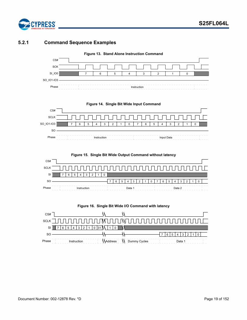
S25FL064L
5.2.1 Command Sequence Examples
Figure 13. Stand Alone Instruction Command
Figure 14. Single Bit Wide Input Command
Figure 15. Single Bit Wide Output Command without latency
Figure 16. Single Bit Wide I/O Command with latency
CS#
SCK
SI_IO0
SO_IO1-IO3
Phase
7 6 5 4 3 2 1 0
Instruction
CS#
SCLK
SO_IO1-IO3
SO
Phase
7 6 5 4 3 2 1 0 7 6 5 4 3 2 1 0
Instruction Input Data
CS#
SCLK
SI
SO
Phase
7 6 5 4 3 2 1 0
7 6 5 4 3 2 1 0 7 6 5 4 3 2 1 0
Instruction Data 1 Data 2
CS#
SCLK
SI
SO
Phase
7 6 5 4 3 2 1 0 31 1 0
7 6 5 4 3 2 1 0
Instruction Address Dummy Cycles Data 1

Document Number: 002-12878 Rev. *D Page 20 of 152
S25FL064L
Figure 17. Dual Output Read Command
Figure 18. Quad Output Read Command
Figure 19. Dual I/O Command
Figure 20. Quad I/O Command
Note: 1. The gray bits are optional, the host does not have to drive bits during that cycle.
CS#
SCK
IO0
IO1
Phase
7 6 5 4 3 2 1 0 31 1 0 6 4 2 0 6 4 2 0
7 5 3 1 7 5 3 1
Instruction Address Dummy Cycles Data 1 Data 2
CS#
SCK
IO0
IO1
IO2
IO3
Phase
7 6 5 4 3 2 1 0 31 1 0 4 0 4 0 4 0 4 0 4 0 4
5 1 5 1 5 1 5 1 5 1 5
6 2 6 2 6 2 6 2 6 2 6
7 3 7 3 7 3 7 3 7 3 7
Instruction Address Dummy D1 D2 D3 D4 D5
CS#
SCK
IO0
IO1
Phase
7 6 5 4 3 2 1 0 30 2 0 6 4 2 0 6 4 2 0 6 4 2 0
31 3 1 7 5 3 1 7 5 3 1 7 5 3 1
Instruction Address Mode Dum Data 1 Data 2
CS#
SCLK
IO0
IO1
IO2
IO3
Phase
7 6 5 4 3 2 1 0 28 4 0 4 0 4 0 4 0 4 0 4 0
29 5 1 5 1 5 1 5 1 5 1 5 1
30 6 2 6 2 6 2 6 2 6 2 6 2
31 7 3 7 3 7 3 7 3 7 3 7 3
Instruction Address Mode Dummy D1 D2 D3 D4

Document Number: 002-12878 Rev. *D Page 21 of 152
S25FL064L
Figure 21. Quad I/O Read Command in QPI Mode
Note: 1. The gray bits are optional, the host does not have to drive bits during that cycle.
Figure 22. DDR Quad I/O Read Command
Figure 23. DDR Quad I/O Read Command QPI Mode
Additional sequence diagrams, specific to each command, are provided in Section 8., Commands on page 58.
CS#
SCLK
IO0
IO1
IO2
IO3
Phase
4 0 28 4 0 4 0 4 0 4 0 4 0 4 0
5 1 29 5 1 5 1 5 1 5 1 5 1 5 1
6 2 30 6 2 6 2 6 2 6 2 6 2 6 2
7 3 31 7 3 7 3 7 3 7 3 7 3 7 3
Instruct. Address Mode Dummy D1 D2 D3 D4
CS#
SCK
IO0
IO1
IO2
IO3
Phase
7 6 5 4 3 2 1 0 A-3 8 4 0 4 0 7 6 5 4 3 2 1 0 4 0 4 0
A-2 9 5 1 5 1 7 6 5 4 3 2 1 0 5 1 5 1
A-1 2 6 2 6 2 7 6 5 4 3 2 1 0 6 2 6 2
A 3 7 3 7 3 7 6 5 4 3 2 1 0 7 3 7 3
Instruction Address Mode Dummy DLP D1 D2
CS#
SCLK
IO0
IO1
IO2
IO3
Phase
4 0 A-3 8 4 0 4 0 7 6 5 4 3 2 1 0 4 0 4 0
5 1 A-2 9 5 1 5 1 7 6 5 4 3 2 1 0 5 1 5 1
6 2 A-1 2 6 2 6 2 7 6 5 4 3 2 1 0 6 2 6 2
7 3 A 3 7 3 7 3 7 6 5 4 3 2 1 0 7 3 7 3
Instruct. Address Mode Dummy DLP D1 D2

Document Number: 002-12878 Rev. *D Page 22 of 152
S25FL064L
5.3 Interface StatesThis section describes the input and output signal levels as related to the SPI interface behavior.
Legend
– Z = no driver - floating signal
– HL = Host driving VIL
– HH = Host driving VIH
– HV = either HL or HH
– X = HL or HH or Z
– HT = toggling between HL and HH
– ML = Memory driving VIL
– MH = Memory driving VIH
– MV = either ML or MH
Table 3. Interface States Summary
Interface State VCC SCK CS# RESET# IO3 / RESET#WP# /
IO2SO / IO1 SI / IO0
Power-Off <VCC (low) X X X X X Z X
Low Power
Hardware Data Protection<VCC (cut-off) X X X X X Z X
Power-On (Cold) Reset ≥VCC (min) X HH X X X Z X
Hardware (Warm) Reset Non-Quad Mode
≥VCC (min) X X HL HL X Z X
Hardware (Warm) Reset Quad Mode ≥VCC (min) X HH HL HL X Z X
Interface Standby ≥VCC (min) X HH HH HH X Z X
Instruction Cycle (Legacy SPI)
≥VCC (min) HT HL HH HH HV Z HV
Single Input Cycle
Host to Memory Transfer≥VCC (min) HT HL HH HH X Z HV
Single Latency (Dummy) Cycle ≥VCC (min) HT HL HH HH X Z X
Single Output Cycle
Memory to Host Transfer≥VCC (min) HT HL HH HH X MV X
Dual Input Cycle
Host to Memory Transfer≥VCC (min) HT HL HH HH X HV HV
Dual Latency (Dummy) Cycle ≥VCC (min) HT HL HH HH X X X
Dual Output Cycle
Memory to Host Transfer≥VCC (min) HT HL HH HH X MV MV
Quad Input Cycle
Host to Memory Transfer≥VCC (min) HT HL HH HV HV HV HV
Quad Latency (Dummy) Cycle ≥VCC (min) HT HL HH X X X X
Quad Output Cycle
Memory to Host Transfer≥VCC (min) HT HL HH MV MV MV MV
DDR Quad Input Cycle
Host to Memory Transfer≥VCC (min) HT HL HH HV HV HV HV
DDR Latency (Dummy) Cycle ≥VCC (min) HT HL HH X X X X
DDR Quad Output Cycle
Memory to Host Transfer≥VCC (min) HT HL HH MV MV MV MV

Document Number: 002-12878 Rev. *D Page 23 of 152
S25FL064L
5.3.1 Power-OffWhen the core supply voltage is at or below the VCC (Low) voltage, the device is considered to be powered off. The device does not react to external signals, and is prevented from performing any program or erase operation.
5.3.2 Low Power Hardware Data ProtectionWhen VCC is less than VCC (Cut-off) the memory device will ignore commands to ensure that program and erase operations can not start when the core supply voltage is out of the operating range. When the core voltage supply remains at or below the VCC (Low) voltage for ≥ tPD time, then rises to ≥ VCC (Minimum) the device will begin its Power On Reset (POR) process. POR continues until the end of tPU. During tPU the device does not react to external input signals nor drive any outputs. Following the end of tPU the device transitions to the Interface Standby state and can accept commands. For additional information on POR see Section 12.3.1, Power-On (Cold) Reset on page 131
5.3.3 Hardware (Warm) ResetA configuration option is provided to allow IO3 / RESET# to be used as a hardware reset input when the device is not in any Quad or QPI mode or when it is in any Quad mode or QPI mode and CS# is high. In Quad or QPI mode on some packages a separate reset input is provided (RESET #). When IO3 / RESET# or RESET# is driven low for tRP time the device starts the hardware reset process. The process continues for tRPH time. Following the end of both tRPH and the reset hold time following the rise of RESET# (tRH) the device transitions to the Interface Standby state and can accept commands. For additional information on hardware reset see Section 12.3, Reset on page 131
5.3.4 Interface StandbyWhen CS# is high the SPI interface is in standby state. Inputs other than RESET# are ignored. The interface waits for the beginning of a new command. The next interface state is Instruction Cycle when CS# goes low to begin a new command.
While in interface standby state the memory device draws standby current (ISB) if no embedded algorithm is in progress. If an embedded algorithm is in progress, the related current is drawn until the end of the algorithm when the entire device returns to standby current draw.
5.3.5 Instruction Cycle (Legacy SPI Mode)When the host drives the MSB of an instruction and CS# goes low, on the next rising edge of SCK the device captures the MSB of the instruction that begins the new command. On each following rising edge of SCK the device captures the next lower significance bit of the 8 bit instruction. The host keeps CS# low, and drives the Write Protect (WP#) and IO3 / RESET# signals as needed for the instruction. However, WP# is only relevant during instruction cycles of a WRR or WRAR command or any other commands which affect Status registers, Configuration registers and DLR registers, and is other wise ignored. IO3 / RESET# is driven high when the device is not in Quad Mode (CR1V[1]=0) or QPI Mode (CR2V[3]=0) and hardware reset is not required.
Each instruction selects the address space that is operated on and the transfer format used during the remainder of the command. The transfer format may be Single, Dual O, Quad O, Dual I/O, or Quad I/O, or DDR Quad I/O. The expected next interface state depends on the instruction received.
Some commands are stand alone, needing no address or data transfer to or from the memory. The host returns CS# high after the rising edge of SCK for the eighth bit of the instruction in such commands. The next interface state in this case is Interface Standby.
5.3.6 Instruction Cycle (QPI Mode)In QPI mode, when CR2V[3]=1, instructions are transferred 4 bits per cycle. In this mode instruction cycles are the same as a Quad Input Cycle. See Section 5.3.13, QPP or QOR Address Input Cycle on page 24.
5.3.7 Single Input Cycle - Host to Memory TransferSeveral commands transfer information after the instruction on the single serial input (SI) signal from host to the memory device. The host keeps RESET# high, CS# low, and drives SI as needed for the command. The memory does not drive the Serial Output (SO) signal.
The expected next interface state depends on the instruction. Some instructions continue sending address or data to the memory using additional Single Input Cycles. Others may transition to Single Latency, or directly to Single, Dual, or Quad Output cycle states.

Document Number: 002-12878 Rev. *D Page 24 of 152
S25FL064L
5.3.8 Single Latency (Dummy) CycleRead commands may have zero to several latency cycles during which read data is read from the main Flash memory array before transfer to the host. The number of latency cycles are determined by the Latency Code in the configuration register (CR3V[3:0]). During the latency cycles, the host keeps RESET# and IO3 / RESET# high, CS# low and SCK toggles. The Write Protect (WP#) signal is ignored. The host may drive the SI signal during these cycles or the host may leave SI floating. The memory does not use any data driven on SO or other I/O signals during the latency cycles. The memory does not drive the Serial Output (SO) or I/O signals during the latency cycles.
The next interface state depends on the command structure i.e. the number of latency cycles, and whether the read is single, dual, or quad width.
5.3.9 Single Output Cycle - Memory to Host TransferSeveral commands transfer information back to the host on the single Serial Output (SO) signal. The host keeps RESET# and IO3 / RESET# high, CS# low. The Write Protect (WP#) signal is ignored. The memory ignores the Serial Input (SI) signal. The memory drives SO with data.
The next interface state continues to be Single Output Cycle until the host returns CS# to high ending the command.
5.3.10 Dual Input Cycle - Host to Memory TransferThe Read Dual I/O command transfers two address or mode bits to the memory in each cycle. The host keeps RESET# and IO3 / RESET# high, CS# low. The Write Protect (WP#) signal is ignored. The host drives address on SI / IO0 and SO / IO1.
The next interface state following the delivery of address and mode bits is a Dual Latency Cycle if there are latency cycles needed or Dual Output Cycle if no latency is required.
5.3.11 Dual Latency (Dummy) CycleRead commands may have zero to several latency cycles during which read data is read from the main Flash memory array before transfer to the host. The number of latency cycles are determined by the Latency Code in the configuration register (CR3V[3:0]). During the latency cycles, the host keeps RESET# and IO3 / RESET# high, CS# low, and SCK continues to toggle. The Write Protect (WP#) signal is ignored. The host may drive the SI / IO0 and SO / IO1 signals during these cycles or the host may leave SI /IO0 and SO / IO1 floating. The memory does not use any data driven on SI / IO0 and SO / IO1 during the latency cycles. The host
must stop driving SI / IO0 and SO / IO1 on the falling edge of SCK at the end of the last latency cycle. It is recommended that the host stop driving them during all latency cycles so that there is sufficient time for the host drivers to turn off before the memory begins to drive at the end of the latency cycles. This prevents driver conflict between host and memory when the signal direction changes. The memory does not drive the SI / IO0 and SO / IO1 signals during the latency cycles.
The next interface state following the last latency cycle is a Dual Output Cycle.
5.3.12 Dual Output Cycle - Memory to Host TransferThe Read Dual Output and Read Dual I/O return data to the host two bits in each cycle. The host keeps RESET# and IO3 / RESET# high, CS# low. The Write Protect (WP#) signal is ignored. The memory drives data on the SI / IO0 and SO / IO1 signals during the dual output cycles on the falling edge of SCK.
The next interface state continues to be Dual Output Cycle until the host returns CS# to high ending the command.
5.3.13 QPP or QOR Address Input CycleThe Quad Page Program and Quad Output Read commands send address to the memory only on IO0. The other IO signals are ignored. The host keeps RESET# and IO3 / RESET# high, CS# low, and drives IO0.
For QPP the next interface state following the delivery of address is the Quad Input Cycle. For QOR the next interface state following address is a Quad Latency Cycle if there are latency cycles needed or Quad Output Cycle if no latency is required.

Document Number: 002-12878 Rev. *D Page 25 of 152
S25FL064L
5.3.14 Quad Input Cycle - Host to Memory TransferThe Quad I/O Read command transfers four address or mode bits to the memory in each cycle. In QPI mode the Quad I/O Read and Page Program commands transfer four data bits to the memory in each cycle, including the instruction cycles. The host keeps CS# low, and drives the IO signals.
For Quad I/O Read the next interface state following the delivery of address and mode bits is a Quad Latency Cycle if there are latency cycles needed or Quad Output Cycle if no latency is required. For QPI mode Page Program, the host returns CS# high following the delivery of data to be programmed and the interface returns to standby state.
5.3.15 Quad Latency (Dummy) CycleRead commands may have zero to several latency cycles during which read data is read from the main Flash memory array before transfer to the host. The number of latency cycles are determined by the Latency Code in the configuration register (CR3V[3:0]). During the latency cycles, the host keeps CS# low and continues to toggle SCK. The host may drive the IO signals during these cycles or the host may leave the IO floating. The memory does not use any data driven on IO during the latency cycles. The host must stop driving the IO signals on the falling edge at the end of the last latency cycle. It is recommended that the host stop driving them during all latency cycles so that there is sufficient time for the host drivers to turn off before the memory begins to drive at the end of the latency cycles. This prevents driver conflict between host and memory when the signal direction changes. The memory does not drive the IO signals during the latency cycles.
The next interface state following the last latency cycle is a Quad Output Cycle.
5.3.16 Quad Output Cycle - Memory to Host TransferThe Quad-O and Quad I/O Read returns data to the host four bits in each cycle. The host keeps CS# low. The memory drives data on IO0-IO3 signals during the Quad output cycles.
The next interface state continues to be Quad Output Cycle until the host returns CS# to high ending the command.
5.3.17 DDR Quad Input Cycle - Host to Memory TransferThe DDR Quad I/O Read command sends address, and mode bits to the memory on all the IO signals. Four bits are transferred on the rising edge of SCK and four bits on the falling edge in each cycle. The host keeps CS# low.
The next interface state following the delivery of address and mode bits is a DDR Latency Cycle.
5.3.18 DDR Latency CycleDDR Read commands may have one to several latency cycles during which read data is read from the main Flash memory array before transfer to the host. The number of latency cycles are determined by the Latency Code in the configuration register (CR3V[3:0]). During the latency cycles, the host keeps CS# low. The host may not drive the IO signals during these cycles. So that there is sufficient time for the host drivers to turn off before the memory begins to drive. This prevents driver conflict between host and memory when the signal direction changes. The memory has an option to drive all the IO signals with a Data Learning Pattern (DLP) during the last 4 latency cycles. The DLP option should not be enabled when there are fewer than five latency cycles so that there is at least one cycle of high impedance for turn around of the IO signals before the memory begins driving the DLP. When there are more than 4 cycles of latency the memory does not drive the IO signals until the last four cycles of latency.
The next interface state following the last latency cycle is a DDR Quad Output Cycle, depending on the instruction.
5.3.19 DDR Quad Output Cycle - Memory to Host TransferThe DDR Quad I/O Read command returns bits to the host on all the IO signals. Four bits are transferred on the rising edge of SCK and four bits on the falling edge in each cycle. The host keeps CS# low.
The next interface state continues to be DDR Quad Output Cycle until the host returns CS# to high ending the command.

Document Number: 002-12878 Rev. *D Page 26 of 152
S25FL064L
5.4 Data ProtectionSome basic protection against unintended changes to stored data are provided and controlled purely by the hardware design. These are described below. Other software managed protection methods are discussed in the software section of this document.
5.4.1 Power-UpWhen the core supply voltage is at or below the VCC (Low) voltage, the device is considered to be powered off. The device does not react to external signals, and is prevented from performing any program or erase operation. User is not allowed to enter any valid command during tPU.
5.4.2 Low PowerWhen VCC is less than VCC (Cut-off) the memory device will ignore commands to ensure that program and erase operations can not start when the core supply voltage is out of the operating range.
5.4.3 Clock Pulse CountThe device verifies that all data modifying commands consist of a clock pulse count that is a multiple of eight bit transfers (byte boundary) before executing them. A command not ending on an 8 bit (byte) boundary is ignored and no error status is set for the command.
5.4.4 Deep Power Down (DPD)In DPD mode the device responds only to the Resume from DPD command (RES ABh). All other commands are ignored during DPD mode, thereby protecting the memory from program and erase operations. If the IO3 / RESET# function has been enabled (CR2V[7]=1) or if RESET# is active, IO3 / RESET# or RESET# going low will start a hardware reset and release the device from DPD mode.

Document Number: 002-12878 Rev. *D Page 27 of 152
S25FL064L
6. Address Space Maps
6.1 Overview
6.1.1 Extended AddressThe FL-L family supports 32 bit (4 Byte) addresses to enable higher density devices than allowed by previous generation (legacy) SPI devices that supported only 24 bit (3 Byte) addresses. A 24 bit, byte resolution, address can access only 16 MBytes (128 Mb) maximum density. A 32 bit, byte resolution, address allows direct addressing of up to a 4 GBytes (32 Gbits) address space.
Legacy commands continue to support 24 bit addresses for backward software compatibility. Extended 32 bit addresses are enabled in two ways:
Extended address mode — a volatile configuration register bit that changes all legacy commands to expect 32 bits of address supplied from the host system.
4 Byte address commands — that perform both legacy and new functions, which always expect 32 bit address.
The default condition for extended address mode, after power-up or reset, is controlled by a non-volatile configuration bit. The default extended address mode may be set for 24 or 32 bit addresses. This enables legacy software compatible access to the first 128 Mb of a device or for the device to start directly in 32 bit address mode.
6.1.2 Multiple Address SpacesMany commands operate on the main Flash memory array. Some commands operate on address spaces separate from the main Flash array. Each separate address space uses the full 24 or 32 bit address but may only define a small portion of the available address space.
6.2 Flash Memory ArrayThe main Flash array is divided into uniform erase units called physical Blocks (64 KB), Half Blocks (32 KB) and Sectors (4 KB).
Table 4. S25FL064L Sector Address Map
6.3 ID Address SpaceThe RDID command (9Fh) reads information from a separate Flash memory address space for device identification (ID). See Section 10.2, Device ID Address Map on page 122 for the tables defining the contents of the ID address space. The ID address space is programmed by Cypress and read-only for the host system.
6.3.1 Device Unique IDA 64-bit unique number is located in 8 bytes of the Unique Device ID address space see Table 43, Unique Device ID on page 122. This Unique ID may be used as a software readable serial number that is unique for each device.
Block Size (KByte)
Block Count
Block Range
Half Block Size
(KByte)
Half Block Count
Half Block Range
Sector Size (KByte)
Sector Count
Sector Range
Address Range (Byte Address)
Notes
64 1 BA00
32 1 HBA00 4 1 SA00 0000000h-0000FFFh
Sector Starting Address
—
Sector Ending Address
: : : :
32 2 HBA01 4 16 SA15 000F000h-000FFFFh
: : : : : : : : : :
64 128 BA127
32 255 HBA254 4 2032 SA2031 07F0000h-07F0FFFh
: : : :
32 256 HBA255 4 2048 SA2047 07FF000h-07FFFFFh

Document Number: 002-12878 Rev. *D Page 28 of 152
S25FL064L
6.4 JEDEC JESD216 Serial Flash Discoverable Parameters (SFDP) SpaceThe RSFDP command (5Ah) reads information from a separate Flash memory address space for device identification, feature, and configuration information, in accord with the JEDEC JESD216 standard for Serial Flash Discoverable Parameters. The ID address space is incorporated as one of the SFDP parameters. See Section 10.1, JEDEC JESD216B Serial Flash Discoverable Parameters on page 114 for the tables defining the contents of the SFDP address space. The SFDP address space is programmed by Cypress and read-only for the host system.
6.5 Security Regions Address SpaceEach FL-L family memory device has a 1024 byte Security Regions address space that is separate from the main Flash array. The Security Regions area is divided into 4, individually lockable 256 byte regions. The Security Regions memory space is intended to hold information that can be temporarily protected or permanently locked from further program or erase.
The regions data bytes are erased to FFh when shipped from Cypress. The regions may be programmed and erased like any other Flash memory address space when not protected or locked. Each region can be individually erased. The Security Region Lock Bits (CR1NV[5:2]) are located in the Configuration Register 1. The Security Region Lock Bits are One Time Programmable (OTP) and after being programmed (set to 1) a Lock Bit permanently protects the related region from further erase or programming.
Regions 2 and 3 also have temporary protection from program or erase by the Protection Register (PR) NVLock bit. The NVLock bit is volatile and set or cleared by the IRP logic and commands. See Protection Register (PR) on page 42.
The Security Region Password Protection Bit in the IRP Register (IRP[2]) allows Regions 2 and 3 to be protected from Program and Erase operations until a password is provided. The Security Region Read Protection Bit in the IRP Register (IRP[6]) allows Region 3 to also be protected from Read operations until a password is provided. Attempting to read in a region, that is protected from read, returns invalid and undefined data. See Individual and Region Protection Register (IRP) on page 41.
Attempting to erase or program in a region that is locked or protected will fail with the P_ERR or E_ERR bit in SR2V[6:5] set to “1”. (see Status Register 2 Volatile (SR2V) on page 31 for detail descriptions).
6.6 RegistersRegisters are small groups of memory cells used to configure how the FL-L family memory device operates or to report the status of device operations. The registers are accessed by specific commands. The commands (and hexadecimal instruction codes) used for each register are noted in each register description.
In legacy SPI memory devices the individual register bits could be a mixture of volatile, non-volatile, or One Time Programmable (OTP) bits within the same register. In some configuration options the type of a register bit could change e.g. from non-volatile to volatile.
The FL-L family uses separate non-volatile or volatile memory cell groups (areas) to implement the different register bit types. However, the legacy registers and commands continue to appear and behave as they always have for legacy software compatibility. There is a non-volatile and a volatile version of each legacy register when that legacy register has volatile bits or when the command to read the legacy register has zero read latency. When such a register is read the volatile version of the register is delivered. During Power-On Reset (POR), hardware reset, or software reset, the non-volatile version of a register is copied to the volatile version to provide the default state of the volatile register. When non-volatile register bits are written the non-volatile version of the register is erased and programmed with the new bit values and the volatile version of the register is updated with the new contents of the non-volatile version. When OTP bits are programmed the non-volatile version of the register is programmed and the appropriate bits are updated in the volatile version of the register. When volatile register bits are written, only the volatile version of the register has the appropriate bits updated.
Table 5. Security Region Address Map
Region Byte Address Range (Hex) Initial Delivery State (Hex)
Region 0 000 to 0FF All Bytes = FF
Region 1 100 to 1FF All Bytes = FF
Region 2 200 to 2FF All Bytes = FF
Region 3 300 to 3FF All Bytes = FF

Document Number: 002-12878 Rev. *D Page 29 of 152
S25FL064L
The type for each bit is noted in each register description. The default state shown for each bit refers to the state after power-on reset, hardware reset, or software reset if the bit is volatile. If the bit is non-volatile or OTP, the default state is the value of the bit when the device is shipped from Cypress.
6.6.1 Status Register 1
6.6.1.1 Status Register 1 Non-Volatile (SR1NV) Related Commands: Non-volatile Write Enable (WREN 06h), Write Disable (WRDI 04h), Write Registers (WRR 01h), Read Any Register (RDAR 65h), Write Any Register (WRAR 71h)
Status Register Protect Non-volatile (SRP0_NV) SR1NV[7]: Provides the default state for SRP0. See Status Register Protect (SRP1, SRP0) on page 46.
Sector / Block Protect (SEC_NV) SR1NV[6]: Provides the default state for SEC.
Top or Bottom Protection (TBPROT_NV) SR1NV[5]: Provides the default state for TBPROT.
Legacy Block Protection (BP_NV3, BP_NV2, BP_NV1, BP_NV0) SR1NV[4:2]: Provides the default state for BP_2 to BP_0 bits.
Table 6. Register Descriptions
Register Type Bits Abbreviation
Status Register 1 Non-volatile 7:0 SR1NV[7:0]
Volatile 7:0 SR1V[7:0]
Status Register 1 Volatile 7:0 SR2V[7:0]
Configuration Register 1Non-volatile/OTP 7:0 CR1NV[7:0]
Volatile 7:0 CR1V[7:0]
Configuration Register 2Non-volatile 7:0 CR2NV[7:0]
Volatile 7:0 CR2V[7:0]
Configuration Register 3Non-volatile 7:0 CR3NV[7:0]
Volatile 7:0 CR3V[7:0]
Individual and Region Protection Register OTP 15:0 IRP[15:0]
Password Register OTP 63:0 PASS[63:0]
Individual Block Lock Access Register Volatile 7:0 IBLAR[7:0]
Pointer Region Protection Register Non-volatile 31:0 PRPR[31:0]
DDR Data Learning RegistersOTP 7:0 DLRNV[7:0]
Volatile 7:0 DLRV[7:0]
Table 7. Status Register 1 Non-Volatile (SR1NV)
Bits Field Name Function Type Default State Description
7 SRP0_NV Status Register
Protect 0 Default Non-Volatile 0 Provides the default state for SRP0.
6 SEC_NVSector / Block
ProtectNon-Volatile 0 Provides the defaults state for SEC
5 TBPROT_NV TBPROT Default Non-Volatile 0 Provides the default state for TBPROT
4 BP_NV2 Legacy Block
Protection Default
Non-Volatile 000b Provides the default state for BP bits. 3 BP_NV1
2 BP_NV0
1 WEL_D WEL DefaultNon-Volatile Read Only
0 Provides the default state for the WEL Status. Not user programmable.
0 WIP_D WIP DefaultNon-Volatile Read Only
0 Provides the default state for the WIP Status. Not user programmable.

Document Number: 002-12878 Rev. *D Page 30 of 152
S25FL064L
Write Enable Latch Default (WEL_D) SR1NV[1]: Provides the default state for the WEL Status in SR1V[1]. This bit is programmed by Cypress and is not user programmable.
Write In Progress Default (WIP_D) SR1NV[0]: Provides the default state for the WIP Status in SR1V[0]. This bit is programmed by Cypress and is not user programmable.
6.6.1.2 Status Register 1 Volatile (SR1V) Related Commands: Read Status Register 1(RDSR1 05h), Write Enable for Volatile (WRENV 50h), Write Registers (WRR 01h), Clear Status Register (CLSR 30h), Read Any Register (RDAR 65h), Write Any Register (WRAR 71h). This is the register displayed by the RDSR1 command.
Status Register Protect 0 (SRP0) SR1V[7]: Places the device in the Hardware Protected mode when this bit is set to 1 and the WP# input is driven low. In this mode, any command that change status registers or configuration registers are ignored and not accepted for execution, effectively locking the state of the Status Registers and Configuration Registers SR1NV, SR1V, CR1NV, CR1V, CR2NV, CR2V, CR3NV, DLRNV and DLRV bits, by making the registers read-only. If WP# is high, Status Registers and Configuration Registers SR1NV, SR1V, CR1NV, CR1V, CR2NV, CR2V, CR3NV, DLRNV and DLRV may be changed and Configuration Registers SR1NV, SR1V, CR1NV, CR1V, CR2NV, CR2V, CR3NV, DLRNV and DLRV may be changed. WP# has no effect on the writing of any other registers. SRP0 tracks any changes to the non-volatile version of this bit (SRP0_NV). When QPI or QIO mode is enabled (CR2V[3] or CR1V[1] = “1”) the internal WP# signal level is = 1 because the WP# external input is used as IO2 when either mode is active. This effectively turns off hardware protection. The Register SR1NV, SR1V, CR1NV, CR1V, CR2NV, CR2V, CR3NV, DLRNV and DLRV are unlocked and can be written. See Status Register Protect (SRP1, SRP0) on page 46
Sector / Block Protect (SEC) SR1V[6]: This bit controls if the Block Protect Bits (BP2, BP1, BP0) protect either 4kB Sectors (SEC = “1”) or 64kB Blocks (SEC = “0”). See Section 7.6.1, Legacy Block Protection on page 48 for a description of how the SEC bit value select the memory array area protected.
TBPROT SR1V[5]: This bit defines the reference point of the Legacy Block Protection bits BP2, BP1, and BP0 in the Status Register. As described in the status register section, the BP2-0 bits allow the user to optionally protect a portion of the array, ranging from 1/64, ¼, ½, etc., up to the entire array. When TBPROT is set to a “0” the Legacy Block Protection is defined to start from the top (maximum address) of the array. When TBPROT is set to a “1” the Legacy Block Protection is defined to start from the bottom (zero address) of the array. TBPROT tracks any changes to the non-volatile version of this bit (TBPROT_NV).
Table 8. Status Register 1 Volatile (SR1V)
Bits Field Name
Function Type Default State Description
7 SRP0 Status Register
Protect 0 Volatile
SR1NV
1 = Locks state of SR1NV, SR1V, CR1NV, CR1V, CR2NV, CR2V, CR3NV, DLRNV and DLRVwhen WP# is low, by not executing any commands that would affect SR1NV, SR1V, CR1NV, CR1V, CR2NV, CR2V, CR3NV, DLRNV and DLRV0 = No register protection, even when WP# is low.
6 SECSector / Block
ProtectVolatile
0 = BP2-BP0 protect 64kB blocks1 = BP2-BP0 protect 4kB sectors
5 TBPROT Top or Bottom
Relative Protection
Volatile1 = BP starts at bottom (Low address)0 = BP starts at top (High address)
4 BP2 Legacy Block
Protection Volatile
VolatileProtects the selected range of sectors (Blocks) from Program or Erase.
3 BP1
2 BP0
1 WEL Write Enable
Latch Volatile
Read Only
0 = Not write enabled, no embedded operation can start, 1= Write Enable, embedded operation can startThis bit is not affected by WRR or WRAR, only WREN WRENV, WRDI and CLSR commands affect this bit.
0 WIP Write in Progress Volatile
Read Only
1= Device Busy, an embedded operation is in progress such as program or erase0 = Ready Device is in standby mode and can accept commands This bit is not affected by WRR or WRAR, it only provides WIP status.

Document Number: 002-12878 Rev. *D Page 31 of 152
S25FL064L
Legacy Block Protection (BP2, BP1, BP0) SR1V[4:2]: These bits define the main Flash array area to be protected against program and erase commands. See Section 7.6.1, Legacy Block Protection on page 48 for a description of how the BP bit values select the memory array area protected.
Write Enable Latch (WEL) SR1V[1]: The WEL bit must be set to 1 to enable program, write, or erase operations as a means to provide protection against inadvertent changes to memory or register values. The Write Enable (WREN) command execution sets the Write Enable Latch to a “1” to allow any program, erase, or write commands to execute afterwards. The Write Disable (WRDI) command can be used to set the Write Enable Latch to a “0” to prevent all program, erase, and write commands from execution. The WEL bit is cleared to 0 at the end of any successful program, write, or erase operation. Following a failed operation the WEL bit may remain set and should be cleared with a CLSR command. After a power down / power up sequence, hardware reset, or software reset, the Write Enable Latch is set to a WEL_D. The WRR or WRAR command does not affect this bit.
Write In Progress (WIP) SR1V[0]: Indicates whether the device is performing a program, write, erase operation, or any other operation, during which a new operation command will be ignored. When the bit is set to a “1” the device is busy performing an operation. While WIP is “1”, only Read Status (RDSR1 or RDSR2), Read Any Register (RDAR), Erase / Program Suspend (EPS), Clear Status Register (CLSR), and Software Reset (RSTEN 66h followed by RST 99h) commands are accepted. EPS command will only be accepted if memory array erase or program operations are in progress. The status register E_ERR and P_ERR bits are updated while WIP =1. When P_ERR or E_ERR bits are set to one, the WIP bit will remain set to one indicating the device remains busy and unable to receive new operation commands. A Clear Status Register (CLSR) command must be received to return the device to standby mode. When the WIP bit is cleared to 0 no operation is in progress. This is a read-only bit.
6.6.2 Status Register 2 Volatile (SR2V)Related Commands: Read Status Register 2 (RDSR2 07h), Read Any Register (RDAR 65h). Status Register 2 does not have user programmable non-volatile bits, all defined bits are volatile read only status. The default state of these bits are set by hardware.
Erase Error (E_ERR) SR2V[6]: The Erase Error Bit is used as an Erase operation success or failure indication. When the Erase Error bit is set to a “1” it indicates that there was an error in the last erase operation. This bit will also be set when the user attempts to erase an individual protected main memory sector or erase a locked Security Region. The Chip Erase command will set E_ERR if a protected sector is found during the command execution. When the Erase Error bit is set to a “1” this bit can be cleared to zero with the Clear Status Register (CLSR) command. This is a read-only bit and is not affected by the WRR or WRAR commands.
Program Error (P_ERR) SR2V[5]: The Program Error Bit is used as a program operation success or failure indication. When the Program Error bit is set to a “1” it indicates that there was an error in the last program operation. This bit will also be set when the user attempts to program within a protected main memory sector, or program within a locked Security Region. When the Program Error bit is set to a “1” this bit can be cleared to zero with the Clear Status Register (CLSR) command. This is a read-only bit and is not affected by the WRR or WRAR commands.
Erase Suspend (ES) SR2V[1]: The Erase Suspend bit is used to determine when the device is in Erase Suspend mode. This is a status bit that cannot be written by the user. When Erase Suspend bit is set to “1”, the device is in erase suspend mode. When Erase Suspend bit is cleared to “0”, the device is not in erase suspend mode. Refer to Section 8.6.5, Program or Erase Suspend (PES 75h) on page 94 for details about the Erase Suspend/Resume commands.
Table 9. Status Register 1 Volatile (SR2V)
Bits Field Name Function Type Default State Description
7 RFU Reserved 0 Reserved for Future Use
6 E_ERR Erase Error Occurred
Volatile Read Only
01= Error occurred 0 = No Error
5 P_ERR Programming
Error Occurred Volatile
Read Only0
1 = Error occurred 0 = No Error
4 RFU Reserved 0 Reserved for Future Use
3 RFU Reserved 0 Reserved for Future Use
2 RFU Reserved 0 Reserved for Future Use
1 ES Erase Suspend Volatile
Read Only0
1 = In erase suspend mode. 0 = Not in erase suspend mode.
0 PS Program Suspend
Volatile Read Only
0 1 = In program suspend mode. 0 = Not in program suspend mode.

Document Number: 002-12878 Rev. *D Page 32 of 152
S25FL064L
Program Suspend (PS) SR2V[0]: The Program Suspend bit is used to determine when the device is in Program Suspend mode. This is a status bit that cannot be written by the user. When Program Suspend bit is set to “1”, the device is in program suspend mode. When the Program Suspend bit is cleared to “0”, the device is not in program suspend mode. Refer to Section 8.6.5, Program or Erase Suspend (PES 75h) on page 94 for details.
6.6.3 Configuration Register 1Configuration register 1 controls certain interface and data protection functions. The register bits can be changed using the WRR command with sixteen input cycles or with the WRAR command.
6.6.3.1 Configuration Register 1 Non-volatile (CR1NV)Related Commands: Non-volatile Write Enable (WREN 06h), Write Registers (WRR 01h), Read Any Register (RDAR 65h), Write Any Register (WRAR 71h).
Suspend Erase/Program Status (SUS_D) CR1NV[7]: Provides the default state for the SUS bit in CR1V[7]. This bit is not user programmable.
Complement Protect (CMP_NV) CR1NV[6]: Provides the default state for the CMP bit in CR1V[6].
Security Region Lock Bits (LB3, LB2, LB1, LB0) CR1NV[5:2]: Provide the OTP write protection control of the Security Regions. When an LB bit is set to 1 the related Security Region can no longer be programmed or erased.
Quad Data Width Non-volatile (QUAD_NV) CR1NV[1]: Provides the default state for the QUAD bit in CR1V[1]. The WRR or WRAR command affects this bit. Programming CR1NV[1] =1 will default operation to allow Quad-data-width commands at Power-on or Reset. Status Register Protect 1 Default (SRP1_D) CR1NV[0]: Provides the default state for the SRP1 bit in CR1V[0]. When IRP[2:0]= “111” the SRP1_D OTP bit is user programmable. When SRP1_D =”1” Registers SR1NV, SR1V, CR1NV, CR1V, CR2NV, CR2V, CR3NV, DLRNV and DLRV are permanently locked. See Status Register Protect (SRP1, SRP0) on page 46
Table 10. Configuration Register 1 Non-volatile (CR1NV)
Bits Field Name Function Type Default State
Description
7 SUS_DSuspend Status
DefaultNon-Volatile Read Only
0 Provides the default state for the Suspend Status. Not user programmable.
6 CMP_NVComplement
Protection DefaultNon-Volatile 0 Provides the default state for CMP.
5 LB3
Security Region Lock Bits
OTP
0OTP lock Bits 3:0 for Security Regions 3:00 = Security Region not locked1 = Security Region permanently locked
4 LB2 0
3 LB1 0
2 LB0 0
1 QUAD_NV Quad Default Non-Volatile 0 Provides the default state for QUAD.
0 SRP1_D Status Register Protect
1 DefaultOTP 0
When IRP[2:0]= “111” SRP1_D bit is programmable.Lock current state of SR1NV, SR1V, CR1NV, CR1V, CR2NV, CR2V, CR3NV, DLRNV and DLRV 1 = Registers permanently locked0 = Registers not protected by SRP1 after POR

Document Number: 002-12878 Rev. *D Page 33 of 152
S25FL064L
6.6.3.2 Configuration Register 1 Volatile (CR1V)Related Commands: Read Configuration Register 1 (RDCR1 35h), Write Enable for Volatile (WRENV 50h), Write Registers (WRR 01h), Read Any Register (RDAR 65h), Write Any Register (WRAR 71h). This is the register displayed by the RDCR1 command.
Suspend Status (SUS) CR1V[7]: The Suspend Status bit is used to determine when the device is in Erase or Program suspend mode. This is a status bit that cannot be written by the user. When Suspend Status bit is set to “1”, the device is in erase or program suspend mode. When Suspend Status bit is cleared to “0”, the device is not in erase or program suspend mode. Refer to Section 8.6.5, Program or Erase Suspend (PES 75h) on page 94 for details about the Erase/Program Suspend/Resume commands. Complement Protection (CMP) CR1V[6]: CMP is used in conjunction with TBPROT, BP3, BP2, BP1 and BP0 bits to provide more flexibility for the array protection map, to protect from 1/2 to all of the array.
LB[3:0] CR1V[5:2]: These bits are volatile copies of the related OTP bits of CR1NV. These bits track any changes to the related OTP version of these bits.
Quad Data Width (QUAD) CR1V[1]: When set to 1, this bit switches the data width of the device to 4 bit - Quad mode. That is, WP# becomes IO2 and IO3 / RESET# becomes an active I/O signal when CS# is low or the RESET# input when CS# is high. The WP# input is not monitored for its normal function and is internally set to high (inactive). The commands for Serial, and Dual I/O Read still function normally but, there is no need to drive the WP# input for those commands when switching between commands using different data path widths. Similarly, there is no requirement to drive the IO3 / RESET# during those commands (while CS# is low). The QUAD bit must be set to one when using the Quad Output Read, Quad I/O Read, DDR Quad I/O Read. The volatile register write for QIO mode has a short and well defined time (tQEN) to switch the device interface into QIO mode and (tQEX) to switch the device back to SPI mode. Following commands can then be immediately sent in QIO protocol. While QPI mode is entered or exited by the QPIEN and QPIEX commands, or by setting the CR2V[3] bit to 1, the Quad data width mode is in use whether the QUAD bit is set or not.
Status Register Protect 1(SRP1) CR1V[0]: The SRP1 Bit, when set to 1, protects the current state of the SR1NV, SR1V, CR1NV, CR1V, CR2NV, CR2V, CR3NV, DLRNV and DLRV registers by preventing any write of these registers. See Status Register Protect (SRP1, SRP0) on page 46
As long as the SRP1 bit remains cleared to logic 0 the SR1NV, SR1V, CR1NV, CR1V, CR2NV, CR2V, CR3NV, DLRNV, and DLRV registers are not protected by SRP1. However, these registers may be protected by SRP0 (SR1V[7]) and the WP# input.
Once the SRP1 bit has been written to a logic 1 it can only be cleared to a logic 0 by a power-off to power-on cycle or a hardware reset. Software reset will not affect the state of the SRP1 bit.
The CR1V[0] SRP1 bit is volatile and the default state of SRP1 after power-on comes from SRP1_D in CR1NV[0]. The SRP1 bit can be set in parallel with updating other values in CR1V by a single WRR or WRAR command.
Table 11. Configuration Register 1 Volatile (CR1V)
Bits Field Name Function Type Default State
Description
7 SUS Suspend StatusVolatile
Read Only
CR1NV
1 = Erase / Program suspended0 = Erase / Program not suspended
6 CMPComplement
ProtectionVolatile
0 = Normal Protection Map1 = Inverted Protection Map
5 LB3
Volatile copy of Security Region Lock
Bits
Volatile Read Only
Not user writableSee CR1NV[5:2] OTP lock Bits 3:0 for Security Regions 3:00 = Security Region not locked1 = Security Region permanently locked
4 LB2
3 LB1
2 LB0
1 QUAD Quad I/O mode Volatile 1 = Quad 0 = Dual or Serial
0 SRP1 Status register Protect
1Volatile
Lock current state of SR1NV, SR1V, CR1NV, CR1V, CR2NV, CR2V, CR3NV, DLRNV and DLRV 1 = Registers locked0 = Registers un-locked

Document Number: 002-12878 Rev. *D Page 34 of 152
S25FL064L
6.6.4 Configuration Register 2Configuration register 2 controls certain interface functions. The register bits can be read and changed using the Read Any Register and Write Any Register commands. The non-volatile version of the register provides the ability to set the POR, hardware reset, or software reset state of the controls. The volatile version of the register controls the feature behavior during normal operation.
6.6.4.1 Configuration Register 2 Non-volatile (CR2NV)Related Commands: Non-volatile Write Enable (WREN 06h), Write Registers (WRR 01h), Read Any Register (RDAR 65h), Write Any Register (WRAR 71h).
IO3 _Reset Non-volatile CR2NV[7]: This bit controls the POR, hardware reset, or software reset state of the IO3 signal behavior. Most legacy SPI devices do not have a hardware reset input signal due to the limited signal count and connections available in traditional SPI device packages. The FL-L family provides the option to use the IO3 signal as a hardware reset input when the IO3 signal is not in use for transferring information between the host system and the memory. This non-volatile IO3_Reset configuration bit enables the device to start immediately (boot) with IO3 enabled for use as a RESET# signal.
Output Impedance Non-volatile CR2NV[6:5]: These bits control the POR, hardware reset, or software reset state of the IO signal output impedance (drive strength). Multiple drive strength are available to help match the output impedance with the system printed circuit board environment to minimize overshoot and ringing. These non-volatile output impedance configuration bits enable the device to start immediately (boot) with the appropriate drive strength.
Table 13. Output Impedance Control
Table 12. Configuration Register 2 Non-volatile (CR2NV)
Bits Field Name Function Type Default State
Description
7 IO3R_NV IO3_Reset
Non-volatile
0
1= Enabled -- IO3_RESET is used as IO3 / RESET# input when CS# is high or Quad Mode is disabled CR1V[1]=0 or QPI is disabled (CR3V[3] = 0)0= Disabled -- IO3 has no alternate function, hardware reset is disabled.Provides the default state for the IO3 / RESET# function enable.
6 OI_NV Output Impedance
1 Provides the default output impedance state. See Table 13, Output Impedance Control on page 345 1
4 RFU Reserved 0 Reserved for Future Use
3 QPI_NV QPI 0
1= Enabled -- QPI (4-4-4) protocol in use0= Disabled -- Legacy SPI protocols in use, instruction is always serial on SIProvides the default state for QPI mode.
2 WPS_NVWrite Protect
Selection0
Provides the default state for WPS0= Legacy Protection1= Individual Block Lock
1 ADP_NVAddress Length at
Power-up0
Provides the default state for Address Length1= 4 byte address0= 3 byte address
0 RFU Reserved 0 Reserved for Future Use
CR2NV[6:5] Impedance Selection
Typical Impedance to VSS (Ohms)
Typical Impedance to VCC (Ohms)
Notes
00 18 21
01 26 28
10 47 45
11 71 64 Factory Default

Document Number: 002-12878 Rev. *D Page 35 of 152
S25FL064L
QPI Non-volatile CR2NV[3]: This bit controls the POR, hardware reset, or software reset state of the expected instruction width for all commands. Legacy SPI commands always send the instruction one bit wide (serial I/O) on the SI (IO0) signal. The FL-L family also supports the QPI mode in which all transfers between the host system and memory are 4 bits wide on IO0 to IO3, including all instructions. This non-volatile QPI configuration bit enables the device to start immediately (boot) in QPI mode rather than the legacy serial instruction mode. The recommended procedure for moving to QPI mode is to first use the QPIEN (38h) command, the WRR or WRAR command can also set CR2V[3]=1, QPI mode. The volatile register write for QPI mode has a short and well defined time (tQEN) to switch the device interface into QPI mode and (tQEX) to switch the device back to SPI mode Following commands can then be immediately sent in QPI protocol. The WRAR command can be used to program CR2NV[3]=1, followed by polling of SR1V[0] to know when the programming operation is completed. Similarly, to exit QPI mode use the QPIEX (F5h) command. The WRR or WRAR command can also be used to clear CR2V[3]=0.
Write Protect Selection Non-volatile CR2NV[2]: This bit controls the POR, hardware reset, or software reset state of the Write Protect Method. This non-volatile configuration bit enables the device to start immediately (boot) with Individual Block Lock protection rather than Legacy Block protection.
Address Length at Power-up Non-volatile CR2NV[1]: This bit controls the POR, hardware reset, or software reset state of the expected address length for all commands that require address and are not fixed 3 Byte or 4 Byte only address. Most commands that need an address are legacy SPI commands that traditionally used 3 byte (24 bit) address. For device densities greater than 128 Mb a 4 Byte (32 bit) address is required to access the entire memory array. The address length configuration bit is used to change all 3 Byte address commands to expect 4 Byte address. See Table 32, FL-L Family Command Set (sorted by function) on page 60 for command address length. This non-volatile Address Length configuration bit enables the device to start immediately (boot) in 4 Byte address mode rather than the legacy 3 Byte address mode.
6.6.4.2 Configuration Register 2 Volatile (CR2V)Related Commands: Read Configuration Register 2 (RDCR2 15h), Read Any Register (RDAR 65h), Write Enable for Volatile (WRENV 50h), Write Register (WRR 01h), Write Any Register (WRAR 71h), Enter 4 Byte address mode (4BEN B7h), Exit 4 Byte address mode (4BEX E9h), Enter QPI (38h), Exit QPI (F5h). This is the register displayed by the RDCR2 command.
IO3 Reset CR2V[7]: This bit controls the IO3 / RESET# signal behavior. This volatile IO3 Reset configuration bit enables the use of IO3 as a RESET# input during normal operation when CS# is high or Quad Mode is disabled (CR1V[1] = 0) or QPI is disabled (CR3V[3] = 0).
Table 14. Configuration Register 2 Volatile (CR2V)
Bits Field Name Function Type Default State
Description
7 IO3R IO3_Reset
Volatile
CR2NV
1= Enabled -- IO3 is used as RESET# input when CS# is high or Quad Mode is disabled CR1V[1]=0 or QPI is disabled (CR3V[3] = 0).0= Disabled -- IO3 has no alternate function, hardware reset through IO3 / RESET# input is disabled.
6 OI Output Impedance See Table 13, Output Impedance Control on page 34
5
4 RFU Reserved Reserved for Future Use
3 QPI QPI
1= Enabled -- QPI (4-4-4) protocol in use0= Disabled -- Legacy SPI protocols in use, instruction is always serial on SI
2 WPSWrite Protect
Selection0= Legacy Block Protection1= Individual Block Lock
1 ADPAddress Length at
Power-upVolatile
Read Only
Read Status Only Bit1= 4 byte address0= 3 byte address
0 ADSAddress Length
StatusVolatile CR2NV[1]
Current Address Mode1= 4 byte address0= 3 byte address

Document Number: 002-12878 Rev. *D Page 36 of 152
S25FL064L
Output Impedance CR2V[6:5]: These bits control the IO signal output impedance (drive strength). This volatile output impedance configuration bit enables the user to adjust the drive strength during normal operation.
QPI CR2V[3]: This bit controls the expected instruction width for all commands. This volatile QPI configuration bit enables the device to enter and exit QPI mode during normal operation. When this bit is set to QPI mode, the QUAD mode is active, independent of the setting of QIO mode (CR1V[1]). When this bit is cleared to legacy SPI mode, the QUAD bit is not affected. The QPI CR2V[3] bit can also be set to “1” by the QPIEN (38h) command and set to “0” by the QPIEX (F5h) command.
Write Protect Selection CR2V[2]: This bit selects which Array protection method is used; Legacy Block Protection on page 48) or Individual Block Lock (IBL) Protection on page 51. These volatile configuration bits enable the user to change Protection method during normal operation.
Address Length at Power-on (ADP) CR2V[1]: This bit is read only and shows what the address length will be after power-on reset, hardware reset, or software reset for all commands that require address and are not fixed 3 Byte or 4 Byte address.
Address Length Status (ADS) CR2V[0]: This bit controls the expected address length for all commands that require address and are not fixed 3 Byte or 4 Byte address. See Table 32, FL-L Family Command Set (sorted by function) on page 60 for command address length. This volatile Address Length configuration bit enables the address length to be changed during normal operation. The four byte address mode (4BEN) command directly sets this bit into 4 byte address mode and the (4BEX) command exits sets this bit back into 3 byte address mode. This bit is also updated when the Address Length Non-volatile CR2NV[1] bit is updated.
6.6.5 Configuration Register 3Configuration register 3 controls the main Flash array read commands burst wrap behavior and read latency. The burst wrap configuration does not affect commands reading from areas other than the main Flash array e.g. read commands for registers or Security Regions. The non-volatile version of the register provides the ability to set the start up (boot) state of the controls as the contents are copied to the volatile version of the register during the POR, hardware reset, or software reset. The volatile version of the register controls the feature behavior during normal operation.
The register bits can be read and changed using the, Read Configuration 3 (RDCR3 33h), Write Registers (WRR 01h), Read Any Register (RDAR 65h), Write Any Register (WRAR 71h). The volatile version of the register can also be written by the Set Burst Length (77h) command.
6.6.5.1 Configuration Register 3 Non-volatile (CR3NV)Related Commands: Non-volatile Write Enable (WREN 06h), Write Registers (WRR 01h), Read Any Register (RDAR 65h), Write Any Register (WRAR 71h).
Table 15. QPI and QIO Mode Control Bits
QPI CR2V[3] QUAD CR1V[1] Description
0 0SIO mode: Single and Dual Read, WP#/IO2 input is in use as WP# pin and IO3 / RESET# input is in use as RESET# pin
0 1QIO mode: Single, Dual, and Quad Read, WP#/IO2 input is in use as IO2 and IO3 / RESET# input is in use as IO3 or RESET# pin
1 X QPI mode: Quad Read, WP#/IO2 input is in use as IO2 and IO3 / RESET# input is in use as IO3 or RESET# pin
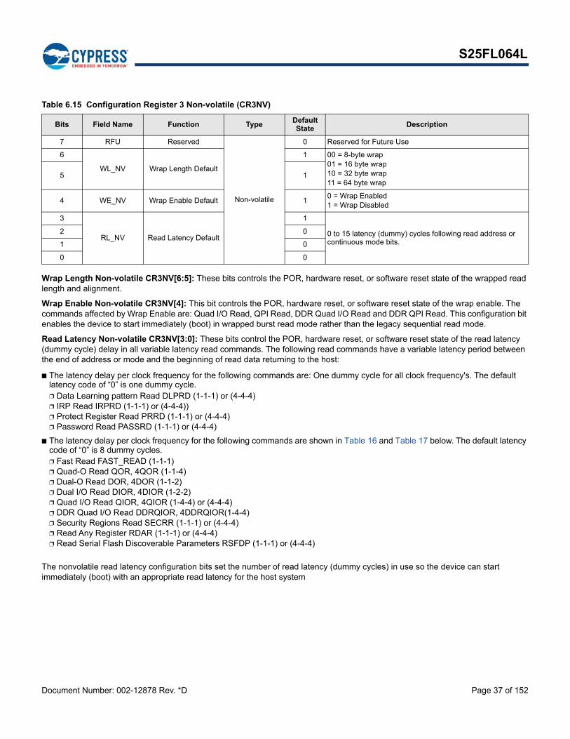
Document Number: 002-12878 Rev. *D Page 37 of 152
S25FL064L
Wrap Length Non-volatile CR3NV[6:5]: These bits controls the POR, hardware reset, or software reset state of the wrapped read length and alignment.
Wrap Enable Non-volatile CR3NV[4]: This bit controls the POR, hardware reset, or software reset state of the wrap enable. The commands affected by Wrap Enable are: Quad I/O Read, QPI Read, DDR Quad I/O Read and DDR QPI Read. This configuration bit enables the device to start immediately (boot) in wrapped burst read mode rather than the legacy sequential read mode.
Read Latency Non-volatile CR3NV[3:0]: These bits control the POR, hardware reset, or software reset state of the read latency (dummy cycle) delay in all variable latency read commands. The following read commands have a variable latency period between the end of address or mode and the beginning of read data returning to the host:
■ The latency delay per clock frequency for the following commands are: One dummy cycle for all clock frequency's. The default latency code of “0” is one dummy cycle. ❐ Data Learning pattern Read DLPRD (1-1-1) or (4-4-4)❐ IRP Read IRPRD (1-1-1) or (4-4-4))❐ Protect Register Read PRRD (1-1-1) or (4-4-4)❐ Password Read PASSRD (1-1-1) or (4-4-4)
■ The latency delay per clock frequency for the following commands are shown in Table 16 and Table 17 below. The default latency code of “0” is 8 dummy cycles. ❐ Fast Read FAST_READ (1-1-1)❐ Quad-O Read QOR, 4QOR (1-1-4)❐ Dual-O Read DOR, 4DOR (1-1-2)❐ Dual I/O Read DIOR, 4DIOR (1-2-2)❐ Quad I/O Read QIOR, 4QIOR (1-4-4) or (4-4-4)❐ DDR Quad I/O Read DDRQIOR, 4DDRQIOR(1-4-4)❐ Security Regions Read SECRR (1-1-1) or (4-4-4)❐ Read Any Register RDAR (1-1-1) or (4-4-4)❐ Read Serial Flash Discoverable Parameters RSFDP (1-1-1) or (4-4-4)
The nonvolatile read latency configuration bits set the number of read latency (dummy cycles) in use so the device can start immediately (boot) with an appropriate read latency for the host system
Table 6.15 Configuration Register 3 Non-volatile (CR3NV)
Bits Field Name Function Type Default State
Description
7 RFU Reserved
Non-volatile
0 Reserved for Future Use
6
WL_NV Wrap Length Default
1 00 = 8-byte wrap01 = 16 byte wrap10 = 32 byte wrap11 = 64 byte wrap
5 1
4 WE_NV Wrap Enable Default 1 0 = Wrap Enabled1 = Wrap Disabled
3
RL_NV Read Latency Default
1
0 to 15 latency (dummy) cycles following read address or continuous mode bits.
2 0
1 0
0 0

Document Number: 002-12878 Rev. *D Page 38 of 152
S25FL064L
.
Table 16. Latency Code (Cycles) Versus Frequency Table 1 of 2
Latency Code
0
Read Command Maximum Frequency (MHz)
Fast Read(1-1-1)
Dual-O Read(1-1-2)
Dual I/O Read(1-2-2)
Quad-O Read(1-1-4)
Quad I/O Read(1-4-4)
Quad I/O ReadQPI (4-4-4)
DDR Quad I/O
(1-4-4)QPI (4-4-4)
Mode Cycles = 0 Mode Cycles = 0 Mode Cycles = 4 Mode Cycles = 0 Mode Cycles = 2 Mode Cycles = 2 Mode Cycles = 1
Dummy Cycles = 8
Dummy Cycles = 8
Dummy Cycles= 8
Dummy Cycles= 8
Dummy Cycles= 8
Dummy Cycles = 8
Dummy Cycles = 8
1 50 50 75 35 35 35 20
2 65 65 85 45 45 45 25
3 75 75 95 55 55 55 35
4 85 85 108 65 65 65 45
5 95 95 108 75 75 75 54
6 108 105 108 85 85 85 54
7 108 108 108 95 95 95 54
8 108 108 108 108 108 108 54
9 108 108 108 108 108 108 54
10 108 108 108 108 108 108 54
11 108 108 108 108 108 108 54
12 108 108 108 108 108 108 54
13 108 108 108 108 108 108 54
14 108 108 108 108 108 108 54
15 108 108 108 108 108 108 54
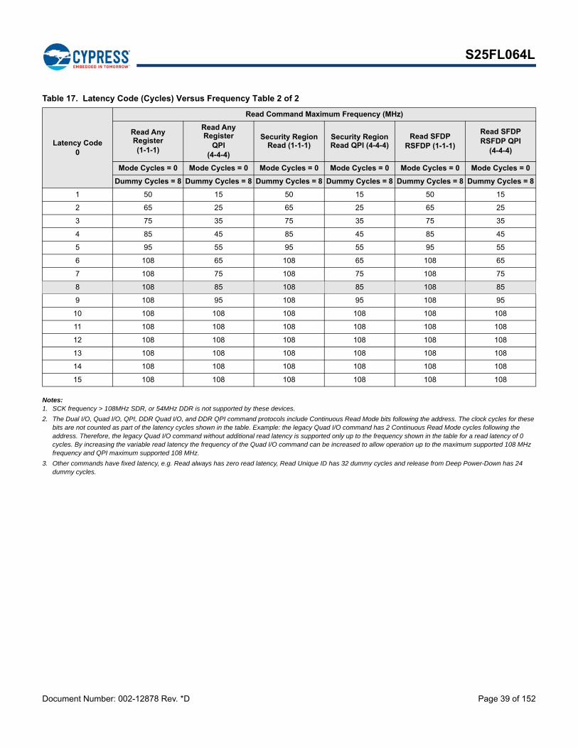
Document Number: 002-12878 Rev. *D Page 39 of 152
S25FL064L
Notes:1. SCK frequency > 108MHz SDR, or 54MHz DDR is not supported by these devices.
2. The Dual I/O, Quad I/O, QPI, DDR Quad I/O, and DDR QPI command protocols include Continuous Read Mode bits following the address. The clock cycles for these bits are not counted as part of the latency cycles shown in the table. Example: the legacy Quad I/O command has 2 Continuous Read Mode cycles following the address. Therefore, the legacy Quad I/O command without additional read latency is supported only up to the frequency shown in the table for a read latency of 0 cycles. By increasing the variable read latency the frequency of the Quad I/O command can be increased to allow operation up to the maximum supported 108 MHz frequency and QPI maximum supported 108 MHz.
3. Other commands have fixed latency, e.g. Read always has zero read latency, Read Unique ID has 32 dummy cycles and release from Deep Power-Down has 24 dummy cycles.
Table 17. Latency Code (Cycles) Versus Frequency Table 2 of 2
Latency Code0
Read Command Maximum Frequency (MHz)
Read Any Register(1-1-1)
Read Any Register
QPI (4-4-4)
Security Region Read (1-1-1)
Security Region Read QPI (4-4-4)
Read SFDP RSFDP (1-1-1)
Read SFDPRSFDP QPI
(4-4-4)
Mode Cycles = 0 Mode Cycles = 0 Mode Cycles = 0 Mode Cycles = 0 Mode Cycles = 0 Mode Cycles = 0
Dummy Cycles = 8 Dummy Cycles = 8 Dummy Cycles = 8 Dummy Cycles = 8 Dummy Cycles = 8 Dummy Cycles = 8
1 50 15 50 15 50 15
2 65 25 65 25 65 25
3 75 35 75 35 75 35
4 85 45 85 45 85 45
5 95 55 95 55 95 55
6 108 65 108 65 108 65
7 108 75 108 75 108 75
8 108 85 108 85 108 85
9 108 95 108 95 108 95
10 108 108 108 108 108 108
11 108 108 108 108 108 108
12 108 108 108 108 108 108
13 108 108 108 108 108 108
14 108 108 108 108 108 108
15 108 108 108 108 108 108

Document Number: 002-12878 Rev. *D Page 40 of 152
S25FL064L
6.6.5.2 Configuration Register 3 Volatile (CR3V)Related Commands: Read Configuration 3 (RDCR3 33h), Write Enable for Volatile (WRENV 50h), Write Registers (WRR 01h), Read Any Register (RDAR 65h), Write Any Register (WRAR 71h), Set Burst Length (SBL 77h). This is the register displayed by the RDCR3 command.
Wrap Length CR3V[6:5]: These bits controls the wrapped read length and alignment during normal operation. These volatile configuration bits enable the user to adjust the burst wrapped read length during normal operation.
Wrap Enable CR3V[4]: This bit controls the burst wrap feature. This volatile configuration bit enables the device to enter and exit burst wrapped read mode during normal operation. When CR3V[4]=1, the wrap mode is not enabled and unlimited length sequential read is performed. When CR3V[4]=0, the wrap mode is enabled and a fixed length and aligned group of 8, 16, 32, or 64 bytes is read starting at the byte address provided by the read command and wrapping around at the group alignment boundary.
Read Latency CR3V[3:0]: These bits set the read latency (dummy cycle) delay in variable latency read commands. These volatile configuration bits enable the user to adjust the read latency during normal operation to optimize the latency for different commands or, at different operating frequencies, as needed.
Table 18. Configuration Register 3 Volatile (CR3V)
Bits Field Name Function Type Default State
Description
7 RFU Reserved
Volatile CR3NV
Reserved for Future Use
6
WL Wrap Length
00 = 8-byte wrap01 = 16 byte wrap10 = 32 byte wrap11 = 64 byte wrap
5
4 WE Wrap Enable0 = Wrap Enabled1 = Wrap Disabled
3
RL Read Latency0 to 15 latency (dummy) cycles following read address or continuous mode bits.
2
1
0

Document Number: 002-12878 Rev. *D Page 41 of 152
S25FL064L
6.6.6 Individual and Region Protection Register (IRP)Related Commands: IRP Read (IRPRD 2Bh) and IRP Program (IRPP 2Fh), Read Any Register (RDAR 65h), Write Any Register (WRAR 71h).
The IRP register is a 16 bit OTP memory location used to permanently configure the behavior of Individual and Region Protection (IRP) features. IRP does not have user programmable volatile bits, all defined bits are OTP.
The default state of the IRP bits are programmed by Cypress.
Security Regions Read Password Mode Enable (SECRRP) IRP[6]: When programmed to “0”, SECRRP enables the Security Region 3 read password mode when PWDMLB bit IRP[2] is program at same time or later. The SECRRP bit can only be programmed when IRP[2:0] = “111”, if not programming will fail with P_ERR set to 1. See Section 7.7.4, Security Region Read Password Protection on page 57.
IBL Lock Boot Bit (IBLLBB) IRP[4]: The default state is 1, all individual IBL bits are set to “0” in the protected state, following power-up, hardware reset, or software reset. In order to Program or Erase the Array the Global IBL Unlock or the Sector / Block IBL Unlock command must be given before the Program or Erase commands. When programmed to 0, all the individual IBL bits are in the un-protected state following power-up, hardware reset, or software reset. The IBLLBB bit can only be programmed when IRP[2:0] = “111”, if not programming will fail with P_ERR set to “1”. See Section 7.6.2, Individual Block Lock (IBL) Protection on page 51.
Password Protection Mode Lock Bit (PWDMLB) IRP[2]: When programmed to “0”, the Password Protection Mode is permanently selected to protect the Security Regions 2 and 3 and Pointer Region. The PWDMLB bit can only be programmed when IRP[2:0] = “111”, if not programming will fail with P_ERR set to 1. See Section 7.7.3, Password Protection Mode on page 56.
After the Password protection mode is selected by programming IRP[2] = “0”, the state of all IRP bits are locked and permanently protected from further programming. Attempting to program any IRP bits will result in a programming error with P_ERR set to 1.
The Password must be programmed and verified, before the Password Mode (IRP[2]=0) is set.
Table 19. IRP Register (IRP)
Bits Field Name Function Type Default State
Description
15 to 7 RFU Reserved OTP All bits are
1Reserved for Future Use
6 SECRRP Security Region 3 Read Password Mode Enable Bit
OTP 10 = Security Region 3 Read password mode selected 1 = Security Region 3 Read Password not selectedIRP[6] is programmable if IRP[2:0]= “111”
5 RFU Reserved OTP 1 Reserved for Future Use
4 IBLLBB IBL Lock Boot Bit OTP 1
0 = All individual IBL bits are set to “1” at power-up in the unprotected state 1 = All individual IBL bits are set to “0” at power-up in the protected state IRP[4] is programmable if IRP[2:0]= “111”
3 RFU Reserved OTP 1 Reserved for Future Use
2 PWDMLB
Password Protection Mode
Lock Bit OTP 1 0 = Password Protection Mode permanently enabled. 1 = Password Protection Mode not permanently enabled.IRP[2] is programmable if IRP[2:0]= “111”
1 PSLMLB
Power Supply Lock-down
protection Mode Lock Bit
OTP 1
0 = Power Supply Lock-down protection Mode permanently enabled.1 = Power Supply Lock-down protection Mode not permanently enabled.IRP[1] is programmable if this is enabled by IRP[2:0]= “111”
0 PERMLB
Permanent Protection Lock
OTP 1 0 = Permanent Protection Mode permanently enabled. 1 = Permanent Protection Mode not permanently enabled. IRP[0] is programmable if IRP[2:0]= “111”

Document Number: 002-12878 Rev. *D Page 42 of 152
S25FL064L
Power Supply Lock-down protection Mode Lock Bit (PSLMLB) IRP[1]: When programmed to 0, the Power Supply Lock-down protection Mode is permanently selected. The PSLMLB bit can only be programmed when IRP[2:0] = “111”, if not programming will fail with P_ERR set to “1”.
After the Power Supply Lock-down protection mode is selected by programming IRP[1] = 0”, the state of all IRP bits are locked and permanently protected from further programming. Attempting to program any IRP bits will result in a programming error with P_ERR set to “1”. See Section 7.7.1, IRP Register on page 55
Permanent Protection Lock Bit (PERMLB) IRP[0]: When programmed to 0, the Permanent Protection Lock Bit permanently protects the Pointer Region and Security Regions 2 and 3, This bit provides a simple way to permanently protect the Pointer Region and Security Regions 2 and 3 without the use of a password or the PRL command. See Section 7.7.1, IRP Register on page 55
PWDMLB (IRP[2]), PSLMLB (IRP[1]) and PERMLB(IRP[0]) are mutually exclusive, only one may be programmed to zero. IRP bits may only be programmed while IRP[2:0] = “111”. Attempting to program IRP bits when IRP[2:0] is not = “111” will result in a programming error with P_ERR set to “1”. The IRP protection mode should be selected during system configuration to ensure that a malicious program does not select an undesired protection mode at a later time. By locking all the protection configuration via the IRP mode selection, later alteration of the protection methods by malicious programs is prevented.
6.6.7 Password Register (PASS)Related Commands: Password Read (PASSRD E7h) and Password Program (PASSP E8h), Read Any Register (RDAR 65h), Write Any Register (WRAR 71h). The PASS register is a 64 bit OTP memory location used to permanently define a password for the Individual and Region Protection (IRP) feature. PASS does not have user programmable volatile bits, all defined bits are OTP. A volatile copy of PASS is used to satisfy read latency requirements but the volatile register is not user writable or further described. The Password can not be read or programmed after IRP[2] is programmed to “0”. See Table 19, IRP Register (IRP) on page 41.
6.6.8 Protection Register (PR)Related Commands: Protection Register Read (PRRD A7h) Protection Register Lock (PRL A6h), Read Any Register (RDAR 65h).
PR does not have separate user programmable non-volatile bits, all defined bits are volatile read only status. The default state of the RFU bits is set by hardware. There is no non-volatile version of the PR register.
The NVLOCK bit is used to protect the Security Regions 2 and 3 and Pointer Region Protection. When NVLOCK[0] = 0, the Security Regions 2 and 3 and Pointer Region Protection can not be changed.
Table 20. Password Register (PASS)
Bits Field Name
Function Type Default State Description
63 to 0 PWD Hidden
Password OTP
FFFFFFFF-FFFFFFFFh
Non-volatile OTP storage of 64 bit password. The password is no longer readable after the password protection mode is selected by programming IRP register bit 2 to zero.

Document Number: 002-12878 Rev. *D Page 43 of 152
S25FL064L
Note:1. The Command Protection Register Lock (PRL), sets the NVLOCK =”1”.
6.6.9 Individual Block Lock Access Register (IBLAR)Related Commands: IBL Read (IBLRD 3Dh or 4IBLRD E0h), IBL Lock (IBL 36h or 4IBL E1h), IBL Unlock (IBLUL 39h or 4IBUL E2h), Global IBL lock (GBL 7Eh), Global IBL unlock (GBUL 98h).
IBLAR does not have user programmable non-volatile bits, all bits are a representation of the volatile bits in the IBL array. The default state of the IBL array bits is set by hardware. There is no non-volatile version of the IBLAR register.
Notes:1. See Figure 25, Individual Block Lock / Pointer Region Protection Control on page 51.
2. The IBL bits maybe read by the IBLRD and 4IBLRD commands.
Table 21. Protection Status Register (PR)
Bits Field Name Function Type Default State Description
7 RFU Reserved
VolatileRead Only
00h Reserved for Future Use
6 SECRRPSecurity Regions Read Password
IRP[6]0 = Security Region 3 password protected from read when NVLOCK = 01 = Security Region 3 not password protected from read
5 RFU Reserved 0 Reserved for Future Use
4 RFU Reserved 0 Reserved for Future Use
3 RFU Reserved 0 Reserved for Future Use
2 RFU Reserved 0 Reserved for Future Use
1 RFU Reserved 0 Reserved for Future Use
0 NVLOCK Protect Non-volatile
configurationIRP[2] and IRP[0]
0 = Security Regions 2 and 3 and Pointer Region write protected 1 = Security Regions 2 and 3 and Pointer Region may be written. 1
Table 22. IBL Access Register (IBLAR)
Bits Field Name Function Type Default State Description
7 to 0 IBL Read or write IBL
for individual sectors / blocks
Volatile IRP[4]=1 then
00helse FFh
00h = IBL for the sector / block addressed is set to “0” by the IBL, 4IBL and GBL commands protecting that sector from program or erase operations. FFh = IBL for the sector / block addressed is cleared to “1” by the IBUL, 4IBUL and GBUL commands not protecting that sector from program or erase operations.

Document Number: 002-12878 Rev. *D Page 44 of 152
S25FL064L
6.6.10 Pointer Region Protection Register (PRPR)Related Commands: Set Pointer Region (SPRP FBh or 4SPRP E3h), Read Any Register (RDAR 65h), Write Any Register (WRAR 71h).
PRPR contains user programmable non-volatile bits. The default state of the PRPR bits is set by hardware. There is no volatile version of the PRPR register. See Section 7.6.3, Pointer Region Protection (PRP) on page 52 for additional details.
6.6.11 DDR Data Learning RegistersRelated Commands: Program DLRNV (PDLRNV 43h), Write DLRV (WDLRV 4Ah), Data Learning Pattern Read (DLPRD 41h), Read Any Register (RDAR 65h), Write Any Register (WRAR 71h).
The Data Learning Pattern (DLP) resides in an 8-bit Non-Volatile Data Learning Register (DLRNV) as well as an 8-bit Volatile Data Learning Register (DLRV). When shipped from Cypress, the DLRNV value is 00h. Once programmed, the DLRNV cannot be reprogrammed or erased; a copy of the data pattern in the DLRNV will also be written to the DLRV. The DLRV can be written to at any time, but on hardware and software reset or power cycles the data pattern will revert back to what is in the DLRNV. During the learning phase described in the SPI DDR modes, the DLP will come from the DLRV. Each IO will output the same DLP value for every clock edge. For example, if the DLP is 34h (or binary 00110100) then during the first clock edge all IO’s will output 0; subsequently, the 2nd clock edge all I/O’s will output 0, the 3rd will output 1, etc.
When the DLRV value is 00h, no preamble data pattern is presented during the dummy phase in the DDR commands.
Table 23. PRP Register (PRPR)
Bits Field Name Function Type Default State Description
A31 to A23 RFU Reserved
Non-volatile
11111111b Reserved for Future Use
A22 to A16 PRPAD PRP Address FFh Pointer Address A22 to A16
A15 to A12 Fh Pointer Address A15 to A12
A11 PRPALL PRP Protect All 10=Protect Pointer Region selected sectors1=Protect All sectors
A10 PRPEN PRP Enable 10=Enable Pointer Region Protection1=Disable Pointer Region Protection
A9 PRPTB PRP Top/Bottom 10=Pointer Region Protection starts from the top (high address)1=Pointer Region Protection starts from the bottom (low address)
A8 RFU Reserved 1 Reserved for Future Use
A7 to A0 RFU Reserved FFh Reserved for Future Use
Table 24. Non-Volatile Data Learning Register (DLRNV)
Bits Field Name
Function Type Default State Description
7 to 0 NVDLP Non-Volatile Data Learning Pattern
OTP 00h OTP value that may be transferred to the host during DDR read command latency (dummy) cycles to provide a training pattern to help the host more accurately cen-ter the data capture point in the received data bits.
Table 25. Volatile Data Learning Register (DLRV)
Bits Field Name
Function Type Default State Description
7 to 0 VDLP Volatile Data
Learning Pattern Volatile
Takes the value of DLRNV
during POR or Reset
Volatile copy of the NVDLP used to enable and deliver the Data Learning Pattern (DLP) to the outputs. The VDLP may be changed by the host during system opera-tion.

Document Number: 002-12878 Rev. *D Page 45 of 152
S25FL064L
7. Data Protection
7.1 Security Regions The device has a 1024 byte address space that is separate from the main Flash array. This area is divided into 4, individually lockable, 256 byte length regions. See Section 6.5, Security Regions Address Space on page 28.
The Security Region memory space is intended for increased system security. The data values can “mate” a flash component with the system CPU/ASIC to prevent device substitution. The Security Region address space is protected by the Security Region Lock bits or the Protection Register NVLOCK bit (PR[0]). See Section 7.1.4, Security Region Lock Bits (LB3, LB2, LB1, LB0) on page 45.
7.1.1 Reading Security Region Memory RegionsThe Security Region Read command (SECRR) uses the same protocol as Fast Read. Read operations outside the valid 1024 byte Security Region address range will yield indeterminate data. See Section 8.7.3, Security Regions Read (SECRR 48h) on page 98.
Security Region 3 may be password protected from read by setting the PWDMLB bit IRP[2] = 0 and SECRRP bit IRP[6] = 0 when NVLOCK = 0.
7.1.2 Programming the Security Regions The protocol of the Security Region programming command (SECRP) is the same as Page Program. See Section 8.7.2, Security Region Program (SECRP 42h) on page 98
The valid address range for Security Region Program is depicted in Table 5 on page 28. Security Region Program operations outside the valid Security Region address range will be ignored, without P_ERR in SR2V[5] set to “1”.
Security Regions 2 and 3 may be password protected from programming by setting the PWDMLB bit IRP[2] = 0.
7.1.3 Erasing the Security Regions The protocol of the Security Region erasing command (SECRE) is the same as Sector erase. See Section 8.7.1, Security Region Erase (SECRE 44h) on page 97
The valid address range for Security Region Erase is depicted in Table 5 on page 28. Security Region Erase operations outside the valid Security Region address range will be ignored, without E_ERR in SR2V set to “1”.
Security Regions 2 and 3 may be password protected from erasing by setting the PWDMLB bit IRP[2] = 0.
7.1.4 Security Region Lock Bits (LB3, LB2, LB1, LB0)The Security Region Lock Bits (LB3, LB2, LB1, LB0) are non-volatile One Time Program (OTP) bits in Configuration Register 1(CR1NV[5:2]) that provide the write protect control and status to the Security Regions. The default state of Security Regions 0 to 3 are unlocked. LB[3:0] can be set to 1 individually using the Write Status Registers or Write Any Register command. LB[3:0] are One Time Programmable (OTP), once it’s set to 1, the corresponding 256 Byte Security Region will become read-only permanently.
7.2 Deep Power Down The Deep Power Down (DPD) command offers an alternative means of data protection as all commands are ignored during the DPD state, except for the Release from Deep Power Down (RES ABh) command and hardware reset. Thus, preventing any program or erase during the DPD state.

Document Number: 002-12878 Rev. *D Page 46 of 152
S25FL064L
7.3 Write Enable Commands
7.3.1 Write Enable (WREN)The Write Enable (WREN) command must be written prior to any command that modifies non-volatile data. The WREN command sets the Write Enable Latch (WEL) bit. The WEL bit is cleared to 0 (disables writes) during power-up, hardware and software reset, or after the device completes the following commands:
Reset
Page Program (PP or 4PP)
Quad Page Program (QPP or 4QPP)
Sector Erase (SE or 4SE)
Half Block Erase (HBE or 4HBE)
Block Erase (BE or 4BE)
Chip Erase (CE)
Write Disable (WRDI)
Write Registers (WRR)
Write Any Register (WRAR)
Security Region Erase (SECRE)
Security Region Byte Programming (SECRP)
Individual and Region Protection Register Program (IRPP)
Password Program (PASSP)
Clear Status Register (CLSR)
Set Pointer Region Protection (SPRP or 4SPRP)
Program Non-Volatile Data Learning Register (PDLRNV)
Write Volatile Data Learning Register (WDLRV)
7.3.2 Write Enable for Volatile Registers (WRENV)The Write Enable Volatile (WRENV) command must be written prior to Write Register (WRR) command that modifies volatile registers data.
7.4 Write Protect SignalWhen not in Quad mode (CR1V[1] = 0) or QPI mode (CR2V[3] = 0), the Write Protect (WP#) input in combination with the Status Register Protect 0 (SRP0) bit (SR1NV[7]) provide hardware input signal controlled protection. When WP# is Low and SRP0 is set to “1” Status Register 1 (SR1NV and SR1V), Configuration register (CR1NV, CR1V, CR2NV, CR2V and CR3NV) and DDR Data Learning Registers (DLRNV and DLRV) are protected from alteration. This prevents disabling or changing the protection defined by the Legacy Block Protect bits or Security Region Lock Bits. See Section 6.6.1, Status Register 1 on page 29.
7.5 Status Register Protect (SRP1, SRP0)The Status Register Protect bits (SRP1 and SRP0) are volatile bits in the configuration and status registers (CR1V[0] and SR1V[7]). The SRP bits control the method of write protection for SR1NV, SR1V, CR1NV, CR1V, CR2NV, CR2V, CR3NV, DLRNV and DLRV: software protection, hardware protection, or power supply lock-down

Document Number: 002-12878 Rev. *D Page 47 of 152
S25FL064L
Table 26. Status Register Protection Bits (High Security)
Notes:1. SRP0 is reloaded from SRP0_NV (SR1NV[7]) default state after a power-down, power-up cycle, software or hardware reset. To enable hardware protection mode by
the WP# pin at power-up set the SRP0_NV bit to “1”.
2. When SRP1 = 1, a power-down, power-up cycle, or hardware reset, will change SRP1 to 0 as SRP1 is reloaded from SRP1_D.
3. SRP1_D can be written only when IRP[2:0] =”111”. When SRP1_D CR1NV[0]=”1” a power-down, power-up cycle, or hardware reset, will reload SRP1 from SRP1_D = ”1” the volatile bit SRP1 is not writable, thus providing OTP protection. When SRP1_D is programmed to 1, Recommended that SRP0_NV should also be programmed to 1 as an indication that OTP protection is in use.
4. When QPI or QIO mode is enabled (CR2V[3] or CR1V[1] = “1”) the internal WP# signal level is = 1 because the WP# external input is used as IO2 when either mode is active. This effectively turns off hardware protection when SRP1-SRP0 = 01b. The Register SR1NV, SR1V, CR1NV, CR1V, CR2NV, CR2V, CR3NV, DLRNV and DLRV are unlocked and can be written.
5. WIP, WEL, and SUS (SR1[1:0] and CR1[7]) are volatile read only status bits that are never affected by the Write Status Registers command.
6. The non-volatile version of SR1NV, CR1NV, CR2NV and CR3NV are not writable when protected by the SRP bits and WP# as shown in the table. The non-volatile version of these status register bits are selected for writing when the Write Enable (06h) command precedes the Write Status Registers (01h) command or the Write Any Register (71h) command.
7. The volatile version of registers SR1V, CR1V and CR2V are not writable when protected by the SRP bits and WP# as shown in the table. The volatile version of these status register bits are selected for writing when the Write Enable for volatile Status Register (50h) command precedes the Write Status Registers (01h) commandor the Write Enable (06h) command precedes the Write Any Register (71h) command.
8. The volatile CR3V bits are not protected by the SRP bits and may be written at any time by volatile (50h) Write Enable command preceding the Write Status Registers (01h) command. The WRAR (71h) and SBL (77h) commands are alternative ways to write bits in the CR3V register.
9. During system power up and boot code execution: Trusted boot code can determine whether there is any need to change SR1NV, SR1V, CR1NV, CR1V, CR2NV, CR2V, CR3NV, DLRNV and DLRV values. If no changes are needed the SRP1 bit (CR1V[0]) can be set to 1 to protect the SR1NV, SR1V, CR1NV, CR1V, CR2NV, CR2V, CR3NV, DLRNV and DLRV registers from changes during the remainder of normal system operation while power remains on.
SRP1_DCR1NV[0]
SRP1CR1V[0]
SRP0SR1V[7]
WP# Status Register Description
0 0 0 X Software ProtectionWP# pin has no control. SR1NV, SR1V, CR1NV, CR1V, CR2NV, CR2V, CR3NV, DLRNV and DLRV can be written. [Factory Default]
0 0 1 0 Hardware ProtectedWhen WP# pin is low SR1NV, SR1V, CR1NV, CR1V, CR2NV, CR2V, CR3NV, DLRNV and DLRV are locked and can not be written.(1)(4)
0 0 1 1 Hardware UnprotectedWhen WP# pin is high SR1NV, SR1V, CR1NV, CR1V, CR2NV, CR2V, CR3NV, DLRNV and DLRV are unlocked and can be written.(1)
0 1 X X Power Supply Lock-DownSR1NV, SR1V, CR1NV, CR1V, CR2NV, CR2V, CR3NV, DLRNV and DLRV are protected and can not be written to again until the next power-down, power-up cycle. (2)
1 1 X X One Time ProgramSRP1_D CR1NV[0]= 1 SR1NV, SR1V, CR1NV, CR1V, CR2NV, CR2V, CR3NV, DLRNV and DLRV are permanently protected and can not be written.(3)
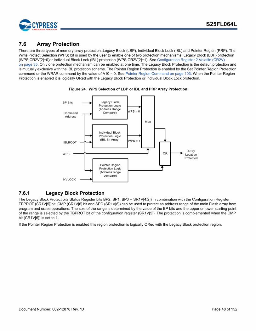
Document Number: 002-12878 Rev. *D Page 48 of 152
S25FL064L
7.6 Array Protection There are three types of memory array protection: Legacy Block (LBP), Individual Block Lock (IBL) and Pointer Region (PRP). The Write Protect Selection (WPS) bit is used by the user to enable one of two protection mechanisms: Legacy Block (LBP) protection (WPS CR2V[2]=0)or Individual Block Lock (IBL) protection (WPS CR2V[2]=1). See Configuration Register 2 Volatile (CR2V) on page 35. Only one protection mechanism can be enabled at one time. The Legacy Block Protection is the default protection and is mutually exclusive with the IBL protection scheme. The Pointer Region Protection is enabled by the Set Pointer Region Protection command or the WRAR command by the value of A10 = 0. See Pointer Region Command on page 103. When the Pointer Region Protection is enabled it is logically ORed with the Legacy Block Protection or Individual Block Lock protection.
Figure 24. WPS Selection of LBP or IBL and PRP Array Protection
7.6.1 Legacy Block ProtectionThe Legacy Block Protect bits Status Register bits BP2, BP1, BP0 -- SR1V[4:2]) in combination with the Configuration Register TBPROT (SR1V[5])bit, CMP (CR1V[6] bit and SEC (SR1V[6]) can be used to protect an address range of the main Flash array from program and erase operations. The size of the range is determined by the value of the BP bits and the upper or lower starting point of the range is selected by the TBPROT bit of the configuration register (SR1V[5]). The protection is complemented when the CMP bit (CR1V[6]) is set to 1.
If the Pointer Region Protection is enabled this region protection is logically ORed with the Legacy Block protection region.
Legacy BlockProtection Logic(Address Range
Compare)
Individual Block Protection Logic(IBL Bit Array)
Mux
OR
Command Address
BP Bits
WPS
Pointer Region Protection Logic(Address range
compare)NVLOCK
Array Location Protected
WPS = 1IBLBOOT
WPS = 0

Document Number: 002-12878 Rev. *D Page 49 of 152
S25FL064L
Table 27. S25FL064L Legacy Block Protection (CMP = 0)
Note:1. X = don’t care
Status Register 64 Mb Block Protection (CMP=0)
SEC TBPROT BP2 BP1 BP0 Protected Block(s) Protected Addresses Protected Density Protected Portion
X X 0 0 0 None None None None
0 0 0 0 1 126 and 127 7E0000h – 7FFFFFh 128 kB Upper 1/64
0 0 0 1 0 124 thru 127 7C0000h – 7FFFFFh 256 kB Upper 1/32
0 0 0 1 1 120 thru 127 780000h – 7FFFFFh 512 kB Upper 1/16
0 0 1 0 0 112 thru 127 700000h – 7FFFFFh 1 MB Upper 1/8
0 0 1 0 1 96 thru 127 600000h – 7FFFFFh 2 MB Upper 1/4
0 0 1 1 0 64 thru 127 400000h – 7FFFFFh 4 MB Upper 1/2
0 1 0 0 1 0 and 1 000000h – 01FFFFh 128 kB Lower 1/64
0 1 0 1 0 0 thru 3 000000h – 03FFFFh 256 kB Lower 1/32
0 1 0 1 1 0 thru 7 000000h – 07FFFFh 512 kB Lower 1/16
0 1 1 0 0 0 thru 15 000000h – 0FFFFFh 1 MB Lower 1/8
0 1 1 0 1 0 thru 31 000000h – 1FFFFFh 2 MB Lower 1/4
0 1 1 1 0 0 thru 63 000000h – 3FFFFFh 4 MB Lower 1/2
X X 1 1 1 0 thru 127 000000h – 7FFFFFh 8 MB ALL
1 0 0 0 1 127 7FF000h – 7FFFFFh 4 kB Upper 1/2048
1 0 0 1 0 127 7FE000h – 7FFFFFh 8 kB Upper 1/1024
1 0 0 1 1 127 7FC000h – 7FFFFFh 16 kB Upper 1/512
1 0 1 0 X 127 7F8000h – 7FFFFFh 32 kB Upper 1/256
1 1 0 0 1 0 000000h – 000FFFh 4 kB Lower 1/2048
1 1 0 1 0 0 000000h – 001FFFh 8 kB Lower 1/1024
1 1 0 1 1 0 000000h – 003FFFh 16 kB Lower 1/512
1 1 1 0 X 0 000000h – 007FFFh 32 kB Lower 1/256

Document Number: 002-12878 Rev. *D Page 50 of 152
S25FL064L
Table 28. S25FL064L Legacy Complement Block Protection (CMP = 1)
Note:1. X = don’t care
Status Register 64Mb Legacy Block Protection (CMP=1)
SEC TBPORT BP2 BP1 BP0 Protected Block(s) Protected Addresses Protected Density Protected Portion
X X 0 0 0 0 thru 127 000000h – 7FFFFFh 8 MB ALL
0 0 0 0 1 0 thru 125 000000h – 7DFFFFh 8,064 kB Lower 63/64
0 0 0 1 0 0 thru 123 000000h – 7BFFFFh 7,936 kB Lower 31/32
0 0 0 1 1 0 thru 119 000000h – 77FFFFh 7,680 kB Lower 15/16
0 0 1 0 0 0 thru 111 000000h – 6FFFFFh 7 MB Lower 7/8
0 0 1 0 1 0 thru 95 000000h – 5FFFFFh 5 MB Lower 3/4
0 0 1 1 0 0 thru 63 000000h – 3FFFFFh 4 MB Lower 1/2
0 1 0 0 1 2 thru 127 020000h – 7FFFFFh 8,064 kB Upper 63/64
0 1 0 1 0 4 thru 127 040000h – 7FFFFFh 7,936 kB Upper 31/32
0 1 0 1 1 8 thru 127 080000h – 7FFFFFh 7,680 kB Upper 15/16
0 1 1 0 0 16 thru 127 100000h – 7FFFFFh 7 MB Upper 7/8
0 1 1 0 1 32 thru 127 200000h – 7FFFFFh 5 MB Upper 3/4
0 1 1 1 0 64 thru 127 400000h – 7FFFFFh 4 MB Upper 1/2
X X 1 1 1 None None None None
1 0 0 0 1 0 thru 127 000000h – 7FEFFFh 8,188 kB Lower 2047/2048
1 0 0 1 0 0 thru 127 000000h – 7FDFFFh 8,184 kB Lower 1023/1024
1 0 0 1 1 0 thru 127 000000h – 7FBFFFh 8,176 kB Lower 511/512
1 0 1 0 X 0 thru 127 000000h – 7F7FFFh 8,160 kB Lower 255/256
1 1 0 0 1 0 thru 127 001000h – 7FFFFFh 8,188 kB Upper 2047/2048
1 1 0 1 0 0 thru 127 002000h – 7FFFFFh 8,184 kB Upper 1023/1024
1 1 0 1 1 0 thru 127 004000h – 7FFFFFh 8,176 kB Upper 511/512
1 1 1 0 X 0 thru 127 008000h – 7FFFFFh 8,160 kB Upper 255/256

Document Number: 002-12878 Rev. *D Page 51 of 152
S25FL064L
7.6.2 Individual Block Lock (IBL) ProtectionIndividual Block Lock Bits (IBL) are volatile, with one bit for each sector / block, and each bit can be individually modified. By issuing the IBL or GBL commands, a IBL bit is set to “0” protecting each related sector / block. By issuing the IBUL or GUL commands, a IBL bit is cleared to “1” unprotecting each related sector or block. By issuing the IBLRD command the state of each IBL bit can be read. This feature allows software to easily protect individual sectors / blocks against inadvertent changes, yet does not prevent the easy removal of protection when changes are needed. The IBL’s can be set or cleared as often as needed as they are volatile bits.
Every main 64KB Block and the 4KB Sectors in bottom and top blocks has a volatile Individual Block Lock Bit (IBL) associated with it. When a sector / block IBL bit is “0”, the related sector/block is protected from program and erase operations.
If the Pointer Region Protection is enabled this protected region is logically ORed with the IBL bits.
Following power-up, hardware reset, or software reset the default state [IBLLBB = 1] (see Table 19, IRP Register (IRP) on page 41) all individual IBL bits are set to “0” in the protected state. In order to Program or Erase the Array the Global IBL Unlock or the Sector / Block IBL Unlock command must be given before the Program or Erase commands. When [IBLLBB = 0], all the individual IBL bits are set to “1” in the un-protected state following power-up, hardware reset, or software reset.
Figure 25. Individual Block Lock / Pointer Region Protection Control
Notes;1. The “M” is the top 64KB Block.
2. The “N is the top 4KB Sector.
Pointer Region Protection EnabledA10 = “0”
Individual Block Lock Bits (IBL) Array
WPS = “1”
Sector N
Log
ica
l OR
Flash Memory
Array
Sector N
Sector N-15Sector N-15
Log
ical
OR
Block M
Block M-1
.........
Block M-1
Logi
cal O
R
Block 1
Block 1
Logi
cal O
R
.........
Sector 15
Sector 0
Block 0
...
Sector 15
Logi
cal O
R
Sector 0
Log
ical
OR
......
......
......
...

Document Number: 002-12878 Rev. *D Page 52 of 152
S25FL064L
7.6.3 Pointer Region Protection (PRP)The Pointer Region Protection is defined by a non-volatile address pointer that selects any 4KB sector as the boundary between protected and unprotected regions in the memory. This provides a protection scheme with individual sector granularity that remains in effect across power cycles and reset operations. PRP settings can also be protected from modification until the next power cycle, until a password is supplied, or can be permanently locked. PRP can be used in combination with either the Legacy Block Protection or Individual Block Lock protection methods. When enabled, PRP protection is logically ORed with the protection method selected by the WPS bit (CR2V[2])
The Set Pointer Region Protection (SPRP FBh or 4SPRP E3h) command (see Section 8.9 on page 103) or Write Any Register (WRAR 71h) command to write the PRPR register (see Section 8.3.15 on page 77) is used to enable or disable PRP, and set the pointer value.
After the Set Block/Pointer Protection command is given or Write Any Register (WRAR 71h) command to write the PRPR register, the value of A10 enables or disables the pointer protection mechanism. If A10 = 1, then the pointer protection region is disabled. This is the default state, and the rest of pointer values are don’t care. If A10=0, then the pointer protection region is enabled. The value of A10 is written in the non-volatile pointer bit in the PRPR. The pointer address values for RFU bits are don’t care but these bit locations will read back as ones. See Section 6.6.10 on page 44 for additional information on the PRPR.
If the pointer protection mechanism is enabled, the pointer value determines the block boundary between the protected and the unprotected regions in the memory. The pointer boundary is set by the three (A23-A12) or four (A31-A12) address bytes written to the non-volatile pointer value in the PRPR. The area that is unprotected will be inclusive of the 4KB sector selected by the pointer value.
The value of A9 is used to determine whether the region that is unprotected will start from the top (highest address) or bottom (lowest address) of the memory array to the location of the pointer. If A9=0 when the SPRP or 4SPRP command is issued followed by a the address, then the 4-kB sector which includes that address and all the sectors from the bottom up (zero to higher address) will be unprotected. If A9=1 when the SPRP or 4SPRPcommand is issued followed by address then the 4-kB sector which includes that address and all the sectors from the Top down (max to lower address) will be unprotected. The value of A9 is in the non-volatile pointer value in the PRPR.
The A11 bit can be used to protect all sectors. If A11=1, then all sectors are protected. If A11=0, then the unprotected range will be determined by Amax-A12. The value of A11 is in the non-volatile pointer value in the PRPR.
The SPRP or 4SPRP command is ignored during a suspend operation because the pointer value cannot be erased and re-programmed during a suspend.
The SPRP or 4SPRP command is ignored if NVLOCK PR[0]=0.
The Read Any Register 65h command (see Section 8.3.14 on page 75) reads the contents of PRP access register. This allows the contents of the pointer to be read out for test and verification.
If the pointer protect scheme is active (A10=0), and the pointer protects any portion of the address space to which an erase command is applied, the erase command fails. For example, if the pointer protection is protecting 4KB of the array that would be affected by a Block erase command, that erase command fails. Chip Erase CEh command is ignored if PRP is enabled (A10=0) and this will set the E_ERR status bit.
If the Pointer Region Protection is enabled this protection is logically ORed with either the Legacy Block protection region if WPS CR2V[2]=0 or Individual Block Lock protection if WPS CR2V[2]=1 (See Figure 24, WPS Selection of LBP or IBL and PRP Array Protection on page 48).
Table 29. PRP Table
A11 A10 A9Protect
Address Range
Unprotect Address Range
Comment
x 1 x None All A10 = 1 is PRP disabled (this is the default state and the rest of pointer value is don't care).
0 0 01FFFFFF to
(A[31:12]+1)
A[31:12]
to 0000000The 4-kB sector which includes that address and all the sectors from the bottom up (zero to higher address) will be unprotected.
0 0 1(A[31;12]-1) to
00000001FFFFFF
to A[31:12]The 4-kB sector which includes that address and all the sectors from the Top down (max to lower address) will be unprotected.
1 0 x1FFFFFF to
000000Not Applicable A10=0 and A11 =1 means protect all sectors and Amax-A12 are don't care.

Document Number: 002-12878 Rev. *D Page 53 of 152
S25FL064L
7.7 Individual and Region ProtectionIndividual and Region Protection (IRP) is the name used for a set of independent hardware and software methods used to disable or enable programming or erase operations on Security Regions 2 and 3 and the Pointer Region Protection Register.
Each method manages the state of the NVLOCK bit (PR[0]). When NVLOCK =1, the Security Regions 2 and 3 and the Pointer Region Protection Register (PRPR) may be programmed and erased. When NVLOCK =0, the Security Regions 2 and 3 and PRPR can not be programmed or erased. Note, the Security Regions 2 and 3 are also protected respectively by LB2 or LB3=1 (CR1NV[4:5]).
Power Supply Lock-down protection is the default method. This method sets the NVLOCK bit to “1” during POR or Hardware Reset so that the NVLOCK related areas and registers are unprotected by a device reset. The PRL (A6h) command clears the NVLOCK bit to “0” to protect the NVLOCK related areas and registers. There is no command in the Power Supply Lock-down method to set the NVLOCK bit to “1”, therefore the NVLOCK bit will remain at “0” until the next power-off or hardware reset. The Power Supply Lock-down method allows boot code the option of changing Security Regions 2 and 3 or the value in PRPR, by programming or erasing these non-volatile areas, then protecting these non-volatile areas from further change for the remainder of normal system operation by clearing the NVLOCK bit to “0”. This is sometimes called Boot-code controlled protection.
The Password method clears the Protection Register NVLOCK bit to 0 and sets the SECRRP bit = IRP[6] during POR or Hardware Reset to protect the NVLOCK related areas and registers. The SECRRP bit determines whether Security Region 3 is readable. A 64 bit password may be permanently programmed and hidden for the password method. The PASSU (EAh) command can be used to provide a password for comparison with the hidden password. If the password matches, the NVLOCK bit is set to “1” to unprotect the NVLOCK related areas and registers. The PRL (A6h) command can be used to clear the NVLOCK bit to “0” to turn on protection again.
The Permanent method permanently sets the SECRRP bit = 1 and clears NVLOCK to 0. This permanently protects the Security Regions 2 and 3 and the PRPR.The selection of the NVLOCK bit management method is made by programming OTP bits in the IRP Register (IRP[2 or 1 or 0] so as to permanently select the method used. An overview of all methods is shown in Figure 26, Permanent, Password and Power Supply Lock-down Protection Overview on page 54.

Document Number: 002-12878 Rev. *D Page 54 of 152
S25FL064L
Figure 26. Permanent, Password and Power Supply Lock-down Protection Overview
Power on Reset orHardware Reset
Password Protection Enabled
IRP[2]=0
Security Region 3 Read
Password Protection EnabledIRP[6]=0
Power Supply Lock-down
Protection EnabledIRP[1]=0
NVLOCK = 0Security Region 3
Read & Write LockedSecurity Region 2
Write LockedPointer Region
Protection Write Locked
Password Unlock
NVLOCK = 1Security Regions 2 & 3
and Pointer Region Protection are UnlockedReadable, Erasable and
Programmable
NVLOCK Bit Write
No
No
Yes
Yes
NVLOCK = 0Security Region 2 & 3
Write LockedPointer Region
Protection Write Locked
Password Unlock
NVLOCK = 1Security Regions 2 & 3
and Pointer Region Protection are Unlocked
Erasable and Programmable
NVLOCK Bit Write
No
No
Yes
Yes
NVLOCK = 1Security Regions 2 & 3
and Pointer Region Protection are UnlockedReadable, Erasable and
Programmable
NVLOCK Bit Write
NVLOCK = 0Security Regions 2 & 3
Write LockedPointer Region
Protection Write Locked
No
Yes
Yes
Yes
NoDefault Power Lock
Protection
IRP Register Bits LockedStatus Register Protect
Locked
IRP Register Bits LockedStatus Register Protect
Locked
IRP Register Bits Programmable
Status Register Protect OTP Option
Programmable
Read Password Protection ModeProtects Security Regions 3 from Read, Erase and Programming, Security Region 2 and Pointer Region Protection from erase and programming after powerup. A password unlock Command will enable changes to Security Region 2 & 3 and Pointer Region Protection. A NVLOCK bit write command turns the protection back on.
Password Protection ModeProtects Security Regions 2 & 3 and Pointer Region Protection from erase and programming after powerup. A password unlock Command will enable changes to Security Region 2 & 3 and Pointer Region Protection. A NVLOCK bit write command turns the protection back on.
Power Supply Lock-down Protection ModeDoes not protect Security Regions 2 & 3 and Pointer Region Protection from erase and programming after powerup. The NVLOCK Bit write command protects Security Regions 2 & 3 and Pointer Region Protection until the next power off or reset.
Default ModeDoes not protect Security Regions 2 & 3 and Pointer Region Protection from erase and programming after powerup. The NVLOCK Bit write command protects Security Regions 2 & 3 and Pointer Region Protection until the next power off or reset. The OTP Option for Status Register Protect is available to be programmed.
Permanent Protection Enabled
IRP[0]=0
IRP Register Bits LockedStatus Register Protect
LockedNVLOCK =0
Permanent Erase and Program Protection of Security Regions 2 & 3
and Pointer Region Protection
No No
Permanent Protection ModePermanently protects Security Regions 2 & 3 and Pointer Region Protection from Erase and Programming
NoteIf Security Region Lock bits LB 2 & 3 are protected CR1NV[5:4]=1, this overrides the NVLOCK and the Security Regions protected by the LB bits will be permanently protected from erase and programming. If Read Password is enabled Security Region 3 can still be read password protected.
Yes Yes
No
NVLOCK = 1Security Regions 2 & 3
and Pointer Region Protection are UnlockedReadable, Erasable and
Programmable
NVLOCK Bit Write
NVLOCK = 0Security Regions 2 & 3
Write LockedPointer Region
Protection Write Locked
No
Yes

Document Number: 002-12878 Rev. *D Page 55 of 152
S25FL064L
7.7.1 IRP RegisterThe IRP register is used to permanently configure the behavior of Individual and Region Protection (IRP) features.
See Table 19, IRP Register (IRP) on page 41.
As shipped from the factory, all devices default to the Power Supply Lock-down protection mode, with all regions unprotected.
The device programmer or host system must then choose which protection method to use by programming one of the one-time programmable bits, Permanent, Power Supply Lock-down or Password Protection Mode. Programming one of these bits locks the part permanently in the selected mode:
Factory Defaults IRP Register
– IRP[6] = “1” = Read Password Protection Mode not enabled.
– IRP[4] = “1” = IBL bits power-up in protected state.
– IRP[2] = “1” = Password Protection Mode not enabled.
– IRP[1] = “1” = Power Supply Lock-down protection Mode not enabled but is the default mode.
– IRP[0] = “1” = Permanent Protection Mode not enabled.
IRP register programming rules:
If the Read Password mode is chosen, the SECRRP bit must be programmed prior or at the same time as setting the Password Protection mode Lock Bits IRP[2].
If the IBL bits power-up in unprotected mode is chosen, the IBLLBB bit must be programmed prior or at the same time as setting one of the Protection mode Lock Bits IRP[2:0].
If the password mode is chosen, the password must be programmed prior to setting the Password Protection mode Lock Bits IRP[2].
The protection modes are mutually exclusive, only one may be selected. Once one of the Protection Modes is selected IPRP[2:0], the IRP Register bits are permanently protected from programming and no further changes to the OTP register bits is allowed. If an attempt to change any of the register bits above, after the Protection mode is selected, the operation will fail and P_ERR (SR2V[5]) will be set to 1.
The programming time of the IRP Register is the same as the typical page programming time. The system can determine the status of the IRP register programming operation by reading the WIP bit in the Status Register. See Section 6.6.1, Status Register 1 on page 29 for information on WIP.
See Section 7.7.3, Password Protection Mode on page 56.
7.7.1.1 IBL Lock Boot BitThe default IBL Lock Bit IRP[4]=1, all the IBL bits on power-up or reset (after a hardware reset or software reset) to the “protected state.” If the IBL Lock Bit IRP[4]=0 (programmed), the IBL power-up or reset to the “unprotected state.”

Document Number: 002-12878 Rev. *D Page 56 of 152
S25FL064L
7.7.2 Protection Register (PR)
7.7.2.1 NVLOCK Bit (PR[0])The NVLOCK bit is a volatile bit for protecting:
Pointer Region Protection Register
Security Regions 2 and 3
When cleared to “0”, NVLOCK locks the related regions. When set to “1”, it allows the related regions to be changed. See Section 6.6.8, Protection Register (PR) on page 42 for more information.
The PRL command is used to clear the NVLOCK bit to “0”. The NVLOCK Bit should be cleared to “0” only after all the related regions are configured to the desired settings.
In Power Supply Lock-down protection mode, the NVLOCK is set to “1” during POR or a hardware reset. A software reset command does not affect the NVLOCK bit. When cleared to “0”, no software command sequence can set the NVLOCK bit to “1”, only another hardware reset or power-up can set the NVLOCK bit.
In the Password Protection mode, the NVLOCK bit is cleared to “0” during POR, or a hardware reset. The NVLOCK bit can only be set to “1” by the Password Unlock command.
The Permanent method permanently clears NVLOCK to 0. This permanently protects the Security Regions 2 and 3 and the PRPR.
7.7.2.2 Security Region Read Password Lock Bit (SECRRP, PR[6])The SECRRP Bit is a volatile bit for read protecting Security Region 3. When SECRRP[6]=0 the Security Region 3 can not be read, See Section 6.6.8, Protection Register (PR) on page 42 for more information.
In the Password Protection mode, the SECRRP bit is set equal to IRP[6] during POR or software or hardware reset. The NVLOCK bit can only be set to “1” by the Password Unlock command. A software reset does not affect the NVLOCK bit.
The Permanent method permanently sets the SECRRP bit = 1. This permanently leaves Security Region 3 readable.
7.7.3 Password Protection ModePassword Protection Mode allows an even higher level of security than the Power Supply Lock-down protection Mode, by requiring a 64-bit password for unlocking the NVLOCK bit. In addition to this password requirement, after power up, hardware reset, the NVLOCK bit is cleared to “0” to ensure protection after power-up or reset. Successful execution of the Password Unlock command by entering the entire password sets the NVLOCK bit to 1, allowing for sector NVLOCK related areas and registers modifications.
Password Protection Notes:
Once the Password is programmed and verified, the Password Mode (IRP[2]=0) must be set in order to prevent reading the password.
The Password Program Command is only capable of programming “0”s. Programming a “1” after a cell is programmed as a “0” results in the cell left as a “0” with no programming error set.
The password is all “1”s when shipped from Cypress. It is located in its own memory space and is accessible through the use of the Password Program, Password Read, RDAR, and WRAR commands.
All 64-bit password combinations are valid as a password.
The Password Mode, once programmed, prevents reading the 64-bit password and further password programming. All further program and read commands to the password region are disabled and these commands are ignored or return undefined data. There is no means to verify what the password is after the Password Mode Lock Bit is selected. Password verification is only allowed before selecting the Password Protection mode.
The Protection Mode Lock Bits are not erasable.
The exact password must be entered in order for the unlocking function to occur. If the password unlock command provided password does not match the hidden internal password, the unlock operation fails in the same manner as a programming operation on a protected sector. The P_ERR bit is set to one, the WIP Bit remains set, and the NVLOCK bit remains cleared to 0.

Document Number: 002-12878 Rev. *D Page 57 of 152
S25FL064L
The Password Unlock command cannot be accepted any faster than once every 100 µs ± 20 µs. This makes it take an unreasonably long time (58 million years) for a hacker to run through all the 64-bit combinations in an attempt to correctly match a password. The Read Status Register 1 command may be used to read the WIP bit to determine when the device has completed the password unlock command or is ready to accept a new password command. When a valid password is provided the password unlock command does not insert the 100 µs delay before returning the WIP bit to zero.
If the password is lost after selecting the Password Mode, there is no way to set the NVLOCK bit =1.
7.7.4 Security Region Read Password ProtectionThe Security Region Read Password Protection enables protecting Security Region 3 from read, program and erase.
Security Region Read Password Protection is an optional addition to the Password Protection Mode (described above). The Security Regions Read Password Protection is enabled when the user programs SECRRP bit ‘IRP[6] = 0. The SECRRP bit IRP[6] must be programmed prior or at the same time as setting the Password Protection mode Lock Bits IRP[2].
The Security Regions Read Password Protection is not active until the password is programmed, IRP[2] is programmed to 0.
When the SECRRP (PR[6]) bit is set to 0 the Security Region 3 is not readable. If these regions are read the resulting data is invalid and undefined.
7.7.5 Recommended IRP Protection ProcessDuring system manufacture, the Flash device configuration should be defined by:
1. Programming the Security Regions as desired.
2. Set Pointer Region Protection Register as desired
3. Program the Password register (PASS) if password protection will be used.
4. Program the IRP Register as desired, including the selection of Permanent, Power Supply Lock-down or password IRP protection mode in IRP[2:0]. It is very important to explicitly select a protection mode so that later accidental or malicious programming of the IRP register is prevented. This is to ensure that only the intended protection features are enabled. Before or while programming the IRP register:
a. The IBLLBB bit (IRP[4]) may be used to cause all the IBL bits to power up in the unprotected state.
b. The SECRRP bit (IRP[6]) may be programmed to select Security Regions Read Password Protection to use the password to control read access to the Security Region 3.
During system power up and boot code execution: If the Power Supply Lock-down protection mode is in use, trusted boot code can determine whether there is any need to modify the NVLOCK related areas or registers. If no changes are needed the NVLOCK bit can be cleared to 0 via the PRL command to protect the NVLOCK related areas or registers from changes during the remainder of normal system operation while power remains on.

Document Number: 002-12878 Rev. *D Page 58 of 152
S25FL064L
8. CommandsAll communication between the host system and FL-L family memory devices is in the form of units called commands. See Section 5.2, Command Protocol on page 17 for details on command protocols.
Although host software in some cases is used to directly control the SPI interface signals, the hardware interfaces of the host system and the memory device generally handle the details of signal relationships and timing. For this reason, signal relationships and timing are not covered in detail within this software interface focused section of the document. Instead, the focus is on the logical sequence of bits transferred in each command rather than the signal timing and relationships. Following are some general signal relationship descriptions to keep in mind. For additional information on the bit level format and signal timing relationships of commands, see Section 5.2, Command Protocol on page 17.
The host always controls the Chip Select (CS#), Serial Clock (SCK), and Serial Input (SI) - SI for single bit wide transfers. The memory drives Serial Output (SO) for single bit read transfers. The host and memory alternately drive the IO0-IO3 signals during Dual and Quad transfers.
All commands begin with the host selecting the memory by driving CS# low before the first rising edge of SCK. CS# is kept low throughout a command and when CS# is returned high the command ends. Generally, CS# remains low for eight bit transfer multiples to transfer byte granularity information. No commands will be accepted if CS# is returned high not at an 8 bit boundary.
8.1 Command Set Summary
8.1.1 Extended Addressing1. Instructions that always require a 4-Byte address, used to access up to 32 Gb of memory:
Table 30. Extended Address 4-Byte Address Commands
2. A 4 Byte address mode for backward compatibility to the 3 Byte address instructions. The standard 3 Byte instructions can be used in conjunction with a 4 Byte address mode controlled by the Address Length configuration bit (CR2V[0]). The default value of CR2V[0] is loaded from CR2NV[1] (following power up, hardware reset, or software reset), to enable default 3-Byte (24-bit) or 4 Byte (32 bit) addressing. When the address length (CR2V[0]) set to 1, the legacy commands are changed to require 4-Bytes (32-bits) for the address field. The following instructions can be used in conjunction with the 4 Byte address mode configuration to switch from 3-Bytes to 4-Bytes of address field.
Command Name Function Instruction (Hex)
4READ Read 13
4FAST_READ Read Fast 0C
4DOR Dual Output Read 3C
4QOR Quad Output Read 6C
4DIOR Dual I/O Read BC
4QIOR Quad I/O Read EC
4DDRQIOR DDR Quad I/O Read EE
4PP Page Program 12
4QPP Quad Page Program 34
4SE Sector Erase 21
4HBE Half Block Erase 53
4BE Block Erase DC
4IBLRD IBL Read E0
4IBL IBL Lock E1
4IBUL IBL Unlock E2
4SPRP Set Pointer Region Protection E3

Document Number: 002-12878 Rev. *D Page 59 of 152
S25FL064L
Table 31. Extended Address 4-Byte Address Mode with 3-Byte Address Commands
Command Name Function Instruction (Hex)
RSFDP Read SFDP 5A
READ Read 03
FAST_READ Read Fast 0B
DOR Dual Output Read 3B
QOR Quad Output Read 6B
DIOR Dual I/O Read BB
QIOR Quad I/O Read EB
DDRQIOR DDR Quad I/O Read) ED
PP Page Program 02
QPP Quad Page Program 32
SE Sector Erase 20
HBE Half Block Erase 52
BE Block Erase D8
RDAR Read Any Register 65
WRAR Write Any Register 71
SECRE Security Region Erase 44
SECRP Security Region Program 42
SECRR Security Region Read 48
IBLRD IBL Read 3D
IBL IBL Lock 36
IBUL IBL Unlock 39
SPRP Set Pointer Region Protection FB
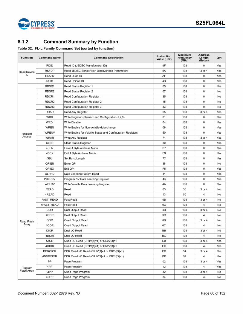
Document Number: 002-12878 Rev. *D Page 60 of 152
S25FL064L
8.1.2 Command Summary by FunctionTable 32. FL-L Family Command Set (sorted by function)
Function Command Name Command Description Instruction Value (Hex)
Maximum Frequency
(MHz)
Address Length (Bytes)
QPI
Read Device ID
RDID Read ID (JEDEC Manufacturer ID) 9F 108 0 Yes
RSFDP Read JEDEC Serial Flash Discoverable Parameters 5A 108 3 or 4 Yes
RDQID Read Quad ID AF 108 0 Yes
RUID Read Unique ID 4B 108 0 Yes
Register Access
RDSR1 Read Status Register 1 05 108 0 Yes
RDSR2 Read Status Register 2 07 108 0 No
RDCR1 Read Configuration Register 1 35 108 0 No
RDCR2 Read Configuration Register 2 15 108 0 No
RDCR3 Read Configuration Register 3 33 108 0 No
RDAR Read Any Register 65 108 3 or 4 Yes
WRR Write Register (Status-1 and Configuration-1,2,3) 01 108 0 Yes
WRDI Write Disable 04 108 0 Yes
WREN Write Enable for Non-volatile data change 06 108 0 Yes
WRENV Write Enable for Volatile Status and Configuration Registers 50 108 0 Yes
WRAR Write Any Register 71 108 3 or 4 Yes
CLSR Clear Status Register 30 108 0 Yes
4BEN Enter 4 Byte Address Mode B7 108 0 Yes
4BEX Exit 4 Byte Address Mode E9 108 0 Yes
SBL Set Burst Length 77 108 0 Yes
QPIEN Enter QPI 38 108 0 No
QPIEX Exit QPI F5 108 0 Yes
DLPRD Data Learning Pattern Read 41 108 0 Yes
PDLRNV Program NV Data Learning Register 43 108 0 Yes
WDLRV Write Volatile Data Learning Register 4A 108 0 Yes
Read Flash Array
READ Read 03 50 3 or 4 No
4READ Read 13 50 4 No
FAST_READ Fast Read 0B 108 3 or 4 No
4FAST_READ Fast Read 0C 108 4 No
DOR Dual Output Read 3B 108 3 or 4 No
4DOR Dual Output Read 3C 108 4 No
QOR Quad Output Read 6B 108 3 or 4 No
4QOR Quad Output Read 6C 108 4 No
DIOR Dual I/O Read BB 108 3 or 4 No
4DIOR Dual I/O Read BC 108 4 No
QIOR Quad I/O Read (CR1V[1]=1) or CR2V[3]=1 EB 108 3 or 4 Yes
4QIOR Quad I/O Read (CR1V[1]=1) or CR2V[3]=1 EC 108 4 Yes
DDRQIOR DDR Quad I/O Read (CR1V[1]=1 or CR2V[3]=1) ED 54 3 or 4 Yes
4DDRQIOR DDR Quad I/O Read (CR1V[1]=1 or CR2V[3]=1) EE 54 4 Yes
Program Flash Array
PP Page Program 02 108 3 or 4 Yes
4PP Page Program 12 108 4 Yes
QPP Quad Page Program 32 108 3 or 4 No
4QPP Quad Page Program 34 108 4 No

Document Number: 002-12878 Rev. *D Page 61 of 152
S25FL064L
Note:1. Commands not supported in QPI mode have undefined behavior if sent when the device is in QPI mode.
Erase Flash Array
SE Sector Erase 20 108 3 or 4 Yes
4SE Sector Erase 21 108 4 Yes
HBE Half Block Erase 52 108 3 or 4 Yes
4HBE Half Block Erase 53 108 4 Yes
BE Block Erase D8 108 3 or 4 Yes
4BE Block Erase DC 108 4 Yes
CE Chip Erase 60 108 0 Yes
CE Chip Erase (alternate instruction) C7 108 0 Yes
Erase /Program
Suspend /Resume
EPS Erase / Program Suspend 75 108 0 Yes
EPR Erase / Program Resume 7A 108 0 Yes
Security Region Array
SECRE Security Region Erase 44 108 3 or 4 Yes
SECRP Security Region Program 42 108 3 or 4 Yes
SECRR Security Region Read 48 108 3 or 4 Yes
Array Protection
IBLRD IBL Read 3D 108 3 or 4 Yes
4IBLRD IBL Read E0 108 4 Yes
IBL IBL Lock 36 108 3 or 4 Yes
4IBL IBL Lock E1 108 4 Yes
IBUL IBL Unlock 39 108 3 or 4 Yes
4IBUL IBL Unlock E2 108 4 Yes
GBL Global IBL Lock 7E 108 0 Yes
GBUL Global IBL Unlock 98 108 0 Yes
SPRP Set Pointer Region Protection FB 108 3 or 4(8.1.3) Yes
4SPRP Set Pointer Region Protection E3 108 4 Yes
Individual and Region Protection
IRPRD IRP Register Read 2B 108 0 Yes
IRPP IRP Register Program 2F 108 0 Yes
PRRD Protection Register Read A7 108 0 Yes
PRL Protection Register Lock (NVLOCK Bit Write) A6 108 0 Yes
PASSRD Password Read E7 108 0 Yes
PASSP Password Program E8 108 0 Yes
PASSU Password Unlock EA 108 0 Yes
Reset
RSTEN Software Reset Enable 66 108 0 Yes
RST Software Reset 99 108 0 Yes
MBR Mode Bit Reset FF 108 0 Yes
Deep Power Down
DPD Deep Power Down B9 108 0 Yes
RES Release from Deep Power Down / Device Id AB 108 0 Yes
Table 32. FL-L Family Command Set (sorted by function) (Continued)
Function Command Name Command Description Instruction Value (Hex)
Maximum Frequency
(MHz)
Address Length (Bytes)
QPI

Document Number: 002-12878 Rev. *D Page 62 of 152
S25FL064L
8.1.3 Read Device IdentificationThere are multiple commands to read information about the device manufacturer, device type, and device features. SPI memories from different vendors have used different commands and formats for reading information about the memories. The FL-L family supports the three device information commands.
8.1.4 Register Read or WriteThere are multiple registers for reporting embedded operation status or controlling device configuration options. There are commands for reading or writing these registers. Registers contain both volatile and non-volatile bits. Non-volatile bits in registers are automatically erased and programmed as a single (write) operation.
8.1.4.1 Monitoring Operation StatusThe host system can determine when a write, program, erase, suspend or other embedded operation is complete by monitoring the Write in Progress (WIP) bit in the Status Register. The Read from Status Register 1 command or Read Any Register command provides the state of the WIP bit. The Read from Status Register 1 or Read Any Register command provides the state of the program error (P_ERR) and erase error (E_ERR) bits in the status register indicate whether the most recent program or erase command has not completed successfully. When P_ERR or E_ERR bits are set to one, the WIP bit will remain set to one indicating the device remains busy and unable to receive most new operation commands. Only status reads (RDSR1 05h, RDSR2 07h), Read Any Register (RDAR 65h), Read Configuration RDCR1, RDCR2 and RDCR3, status clear (CLSR 30h), and software reset (RSTEN 66h followed by RST 99h) are valid commands when P_ERR or E_ERR is set to 1. A Clear Status Register (CLSR) command must be sent to return the device to standby state. Alternatively, Hardware Reset, or Software Reset (RSTEN 66h followed by RST 99h) may be used to return the device to standby state.
8.1.4.2 ConfigurationThere are commands to read, write, and protect registers that control interface path width, interface timing, interface address length, and some aspects of data protection.
8.1.5 Read Flash ArrayData may be read from the memory starting at any byte boundary. Data bytes are sequentially read from incrementally higher byte addresses until the host ends the data transfer by driving CS# input High. If the byte address reaches the maximum address of the memory array, the read will continue at address zero of the array.
Burst Wrap read can be enabled by the Set Burst Length (SBL 77h) command with the requested wrapped read length and alignment, see Section 8.3.16, Set Burst Length (SBL 77h) on page 78. Burst Wrap read is only for Quad I/O and QPI modes
There are several different read commands to specify different access latency and data path widths. Double Data Rate (DDR) commands also define the address and data bit relationship to both SCK edges:
The Read command provides a single address bit per SCK rising edge on the SI/IO0 signal with read data returning a single bit per SCK falling edge on the SO/IO1 signal. This command has zero latency between the address and the returning data but is limited to a maximum SCK rate of 50MHz.
Other read commands have a latency period between the address and returning data but can operate at higher SCK frequencies. The latency depends on a configuration register read latency value.
The Fast Read command provides a single address bit per SCK rising edge on the SI/IO0 signal with read data returning a single bit per SCK falling edge on the SO/IO1 signal.
Dual or Quad Output Read commands provide address on SI/IO0 pin on the SCK rising edge with read data returning two bits, or four bits of data per SCK falling edge on the IO0 - IO3 signals.
Dual or Quad I/O Read commands provide address two bits or four bits per SCK rising edge with read data returning two bits, or four bits of data per SCK falling edge on the IO0 - IO3 signals. Continuous read feature is enabled if the mode bits value is Axh.
Quad Double Data Rate read commands provide address four bits per every SCK edge with read data returning four bits of data per every SCK edge on the IO0 - IO3 signals. Continuous read feature is enabled if the mode bits value is Axh.

Document Number: 002-12878 Rev. *D Page 63 of 152
S25FL064L
8.1.6 Program Flash ArrayProgramming data requires two commands: Write Enable (WREN), and Page Program (PP, 4PP, QPP, 4QPP). The Page Program command accepts from 1 byte up to 256 consecutive bytes of data (page) to be programmed in one operation. Programming means that bits can either be left at 1, or programmed from 1 to 0. Changing bits from 0 to 1 requires an erase operation.
8.1.7 Erase Flash ArrayThe Sector Erase, Half Block Erase, Block Erase, or Chip Erase commands set all the bits in a sector or the entire memory array to 1. A bit needs to be first erased to 1 before programming can change it to a 0. While bits can be individually programmed from a 1 to 0, erasing bits from 0 to 1 must be done on a sector-wide, half block-wide, block-wide or array-wide (Chip) level. The Write Enable (WREN) command must precede an erase command.
8.1.8 Security Regions, Legacy Block Protection, and Individual and Region ProtectionThere are commands to read and program a separate One Time Protection (OTP) array for permanently protected data such as a serial number. There are commands to control a contiguous group (block) of Flash memory array sectors that are protected from program and erase operations.There are commands to control which individual Flash memory array sectors are protected from program and erase operations. There is a mode to limit read access of Security Region 3 until a password is supplied.
8.1.9 ResetThere are commands to reset to the default conditions present after power on to the device. However, the software reset commands do not affect the current state of the SRP1 or NVLOCK Bits. In all other respects a software reset is the same as a hardware reset.
There is a command to reset (exit from) the Continuous Read Mode.
8.1.10 ReservedSome instructions are reserved for future use. In this generation of the FL-L family some of these command instructions may be unused and not affect device operation, some may have undefined results.
Some commands are reserved to ensure that a legacy or alternate source device command is allowed without effect. This allows legacy software to issue some commands that are not relevant for the current generation FL-L family with the assurance these commands do not cause some unexpected action.
Some commands are reserved for use in special versions of the FL-L not addressed by this document or for a future generation. This allows new host memory controller designs to plan the flexibility to issue these command instructions. The command format is defined if known at the time this document revision is published.

Document Number: 002-12878 Rev. *D Page 64 of 152
S25FL064L
8.2 Identification Commands
8.2.1 Read Identification (RDID 9Fh)The Read Identification (RDID) command provides read access to manufacturer identification, device identification. The manufacturer identification is assigned by JEDEC. The device identification values are assigned by Cypress.
Any RDID command issued while a program, erase, or write cycle is in progress is ignored and has no effect on execution of the program, erase, or write cycle that is in progress.
The RDID instruction is shifted on SI / IO0. After the last bit of the RDID instruction is shifted into the device, a byte of manufacturer identification, two bytes of device identification, will be shifted sequentially out on SO / IO1, As a whole this information is referred to as ID. See Section 10.2, Device ID Address Map on page 122 for the detail description of the ID contents.
Continued shifting of output beyond the end of the defined ID address space will provide undefined data. The RDID command sequence is terminated by driving CS# to the logic high state anytime during data output. The RDID command is supported up to 108 MHz.
Figure 27. Read Identification (RDID) Command Sequence
This command is also supported in QPI mode. In QPI mode the instruction is shifted in on IO0-IO3 and the returning data is shifted out on IO0-IO3.
Figure 28. Read Identification (RDID) QPI Mode Command
8.2.2 Read Quad Identification (RDQID AFh)The Read Quad Identification (RDQID) command provides read access to manufacturer identification, device identification. This command is an alternate way of reading the same information provided by the RDID command while in QPI mode. In all other respects the command behaves the same as the RDID command.
The command is recognized only when the device is in QPI Mode (CR2V[3]=1) or Quad Mode (CR1V[1]=1). The instruction is shifted in on IO0-IO3 for QPI Mode and IO0 for Quad Mode. After the last bit of the instruction is shifted into the device, a byte of manufacturer identification, two bytes of device identification will be shifted sequentially out on IO0-IO3. As a whole this information is referred to as ID. See Section 10.2, Device ID Address Map on page 122 for the detail description of the ID contents.
Continued shifting of output beyond the end of the defined ID address space will provide undefined data. The command sequence is terminated by driving CS# to the logic high state anytime during data output.
CS#
SCK
SI_ IO0
SO_IO1
Phase
7 6 5 4 3 2 1 0
7 6 5 4 3 2 1 0 7 6 5 4 3 2 1 0
Instruction Data 1 Data N
CS#
SCLK
IO0
IO1
IO2
IO3
Phase
4 0 4 0 4 0 4 0 4 0 4 0
5 1 5 1 5 1 5 1 5 1 5 1
6 2 6 2 6 2 6 2 6 2 6 2
7 3 7 3 7 3 7 3 7 3 7 3
Instruction D1 D2 D3 D4 Data N

Document Number: 002-12878 Rev. *D Page 65 of 152
S25FL064L
Figure 29. Read Quad Identification (RDQID) Command Sequence QPI Mode
Figure 30. Read Quad Identification (RDQID) Command Sequence Quad Mode
8.2.3 Read Serial Flash Discoverable Parameters (RSFDP 5Ah)The command is initiated by shifting on SI the instruction code “5Ah”, followed by a 24-bit (3 byte) address or 32-bit (4 byte) address (depending on the current Address Length configuration of CR2V[0]), followed by the number of read latency (dummy cycles) set by the Variable Read Latency configuration in CR3V[3:0].
The SFDP bytes are then shifted out on SO/IO1 starting at the falling edge of SCK after the dummy cycles. The SFDP bytes are always shifted out with the MSB first. If the 24-bit (3 byte) address or 32-bit (4 byte) address is set to any non-zero value, the selected location in the SFDP space is the starting point of the data read. This enables random access to any parameter in the SFDP space. In SPI mode the RSFDP command is supported up to 108 MHz.
The Variable Read Latency should be set to 8 cycles for compliance with the JEDEC JESD216 SFDP standard. The non-volatile default Variable Read Latency in CR3NV is set to 8 dummy cycles when the device is shipped from Cypress. However, because the RSFDP command uses the same implementation as other variable address length and latency read commands, users are free to modify the address length and latency of the command if desired.
Continuous (sequential) read is supported with the Read SFDP command.
Figure 31. RSFDP Command Sequence
Note:A = MSB of address = 23 for CR2V[0]=0, or 31 for CR2V[0]=1 or command 13h.
This command is also supported in QPI mode. In QPI mode the instruction is shifted in on IO0-IO3 and the returning data is shifted out on IO0-IO3.
CS#
SCLK
IO0
IO1
IO2
IO3
Phase
4 0 4 0 4 0 4 0 4 0 4 0
5 1 5 1 5 1 5 1 5 1 5 1
6 2 6 2 6 2 6 2 6 2 6 2
7 3 7 3 7 3 7 3 7 3 7 3
Instruction D1 D2 D3 D4 Data N
CS#
SCLK
IO0
IO1
IO2
IO3
Phase
7 6 5 4 3 2 1 0 4 0 4 0
5 1 5 1
6 2 6 2
7 3 7 3
Instruction D1 Data N
CS#
SCK
SI_IO0
SO_IO1
Phase
7 6 5 4 3 2 1 0 A 1 0
7 6 5 4 3 2 1 0
Instruction Address Dummy Cycles Data 1

Document Number: 002-12878 Rev. *D Page 66 of 152
S25FL064L
Figure 32. RSFDP QPI Mode Command Sequence
8.2.4 Read Unique ID (RUID 4Bh)The Read Identification (RUID) command provides read access to factory set read only 64 bit number that is unique to each device.
The RUID instruction is shifted on SI followed by four dummy bytes or 16 dummy bytes QPI (32 clock cycles). This latency period (i.e., dummy bytes) allows the device’s internal circuitry enough time to access data at the initial address. During latency cycles, the data value on IO0-IO3 are “don’t care” and may be high impedance.
Then the 8 bytes of Unique ID will be shifted sequentially out on SO / IO1.
Continued shifting of output beyond the end of the defined Unique ID address space will provide undefined data. The RUID command sequence is terminated by driving CS# to the logic high state anytime during data output.
Figure 33. Read Unique ID (RUID) Command Sequence
This command is also supported in QPI mode. In QPI mode the instruction is shifted in on IO0-IO3 and the returning data is shifted out on IO0-IO3.
Figure 34. Read Unique ID (RUID) QPI Mode Command
CS#
SCLK
IO0
IO1
IO2
IO3
Phase
4 0 20 4 0 4 0 4 0 4 0 4 0
5 1 21 5 1 5 1 5 1 5 1 5 1
6 2 22 6 2 6 2 6 2 6 2 6 2
7 3 23 7 3 7 3 7 3 7 3 7 3
Instruct. Address Dummy D1 D2 D3 D4
CS#
SCK
SI_IO0
SO_IO1
Phase
7 6 5 4 3 2 1 0
636261605958575655 5 4 3 2 1 0
Instruction Dummy Byte 1 Dummy Byte 4 64 bit Unique Serial Number
CS#
SCLK
IO0
IO1
IO2
IO3
Phase
4 0 60 56 4 8 4 0
5 1 61 57 5 9 5 1
6 2 62 58 6 10 6 2
7 3 63 59 7 11 7 3
InstructionDummy 1Dummy 2Dummy 3 Dummy 13Dummy 14Dummy 15Dummy 16 64 bit Unique Serial Number

Document Number: 002-12878 Rev. *D Page 67 of 152
S25FL064L
8.3 Register Access Commands
8.3.1 Read Status Register 1 (RDSR1 05h)The Read Status Register 1 (RDSR1) command allows the Status Register 1 contents to be read from SO/IO1.
The volatile version of Status Register 1 (SR1V) contents may be read at any time, even while a program, erase, or write operation is in progress. It is possible to read Status Register 1 continuously by providing multiples of eight clock cycles. The status is updated for each eight cycle read.
Figure 35. Read Status Register 1 (RDSR1) Command Sequence
This command is also supported in QPI mode. In QPI mode the instruction is shifted in on IO0-IO3 and the returning data is shifted out on IO0-IO3.
Figure 36. Read Status Register 1 (RDSR1) QPI Mode Command
8.3.2 Read Status Register 2 (RDSR2 07h)The Read Status Register 2 (RDSR2) command allows the Status Register 2 contents to be read from SO/IO1.
The volatile Status Register 2 SR2V contents may be read at any time, even while a program, erase, or write operation is in progress. It is possible to read the Status Register 2 continuously by providing multiples of eight clock cycles. The status is updated for each eight cycle read.
Figure 37. Read Status Register 2 (RDSR2) Command
In QPI mode, status register 2 may be read via the Read Any Register command, see Section 8.3.14, Read Any Register (RDAR 65h) on page 75.
CS#
SCK
SI_IO0
SO_IO1
Phase
7 6 5 4 3 2 1 0
7 6 5 4 3 2 1 0 7 6 5 4 3 2 1 0
Instruction Status Updated Status
CS#
SCLK
IO0
IO1
IO2
IO3
Phase
4 0 4 0 4 0 4 0
5 1 5 1 5 1 5 1
6 2 6 2 6 2 6 2
7 3 7 3 7 3 7 3
Instruct. Status Updated Status Updated Status
CS#
SCK
SI_IO0
SO_IO1
Phase
7 6 5 4 3 2 1 0
7 6 5 4 3 2 1 0 7 6 5 4 3 2 1 0
Instruction Status Updated Status

Document Number: 002-12878 Rev. *D Page 68 of 152
S25FL064L
8.3.3 Read Configuration Registers (RDCR1 35h) (RDCR2 15h) (RDCR3 33h)The Read Configuration Register (RDCR1, RDCR2, RDCR3) commands allows the volatile Configuration Registers (CR1V, CR2V, CR3V) contents to be read from SO/IO1.
It is possible to read CR1V, CR2V and CR3V continuously by providing multiples of eight clock cycles. The Configuration Registers contents may be read at any time, even while a program, erase, or write operation is in progress.
Figure 38. Read Configuration Register (RDCR1) (RDCR2) (RDCR3) Command Sequence
In QPI mode, configuration register 1, 2 and 3 may be read via the Read Any Register command, see Section 8.3.14, Read Any Register (RDAR 65h) on page 75.
8.3.4 Write Registers (WRR 01h)The Write Registers (WRR) command allows new values to be written to the Status Register 1, Configuration Register 1, Configuration Register 2 and Configuration Register 3. Before the Write Registers (WRR) command can be accepted by the device, a Write Enable (WREN) or Write Enable for Volatile Registers (WRENV) command must be received. After the Write Enable (WREN) command has been decoded successfully, the device will set the Write Enable Latch (WEL) in the Status Register to enable non-volatile write operations and direct the values in the following WRR command to the non-volatile SR1NV, CR1NV, CR2NV and CR3NV registers. After the Write Enable for Volatile Registers (WRENV) command has been decoded successfully, the device directs the values in the following WRR command to the volatile SR1V, CR1V, CR2V and CRV3 registers.
The Write Registers (WRR) command is entered by shifting the instruction and the data bytes on SI/IO0. The Status Register is one data byte in length.
A WRR operation directed to non-volatile registers by a preceding WREN command, first erases non-volatile registers then programs the new value as a single operation, then copies the new non-volatile values to the volatile version of the registers. A WRR operation directed to volatile registers by a preceding WRENV command, updates the volatile registers without affecting the related non-volatile register values. The Write Registers (WRR) command will set the P_ERR or E_ERR bits if there is a failure in the WRR operation. See Section 6.6.2, Status Register 2 Volatile (SR2V) on page 31 for a description of the error bits. The device hangs busy until clear status register (CLSR) is used to clear the error and WIP for return to standby. Any Status or Configuration Register bit reserved for the future must be written as a “0”.
CS# must be driven to the logic high state after the eighth, sixteenth, twenty-fourth, or thirty-second bit of data has been latched. If not, the Write Registers (WRR) command is not executed. If CS# is driven high after the:
eighth cycle then only the Status Register 1 is written
sixteenth cycle both the Status 1 and Configuration 1 Registers are written;
twenty-fourth cycle Status 1 and Configuration 1 and 2 Registers are written;
thirty-second cycle Status 1and Configuration 1, 2 and 3 Registers are written.
As soon as CS# is driven to the logic high state, the self-timed Write Registers (WRR) operation is initiated. While the Write Registers (WRR) operation is in progress, the Status Register may still be read to check the value of the Write-In Progress (WIP) bit. The Write-In Progress (WIP) bit is a “1” during the self-timed Write Registers (WRR) operation, and is a “0” when it is completed. When the Write Registers (WRR) operation is completed, the Write Enable Latch (WEL) is set to a “0”.
The WRR command is protected from a hardware and software reset, the hardware reset and software reset command are ignored and have no effect on the execution of the WRR command.
CS#
SCK
SI_IO0
SO_IO1
Phase
7 6 5 4 3 2 1 0
7 6 5 4 3 2 1 0 7 6 5 4 3 2 1 0
Instruction Register Read Repeat Register Read

Document Number: 002-12878 Rev. *D Page 69 of 152
S25FL064L
Figure 39. Write Registers (WRR) Command Sequence
This command is also supported in QPI mode. In QPI mode the instruction and data is shifted in on IO0-IO3.
Figure 40. Write Register (WRR) Command Sequence QPI Mode
The Write Registers (WRR) command allows the user to change the values of the Legacy Block Protection bits in either the non-volatile Status Register 1 or in the volatile Status Register 1, to define the size of the area that is to be treated as read-only.
The Write Registers (WRR) command also allows the user to set the Status Register Protect 0 (SRP0) bit to a “1” or a “0”. The Status Register Protect 0 (SRP0) bit and Write Protect (WP#) signal allow the BP bits to be hardware protected.
When the Status Register Protect 0 (SRP0 SR1V[7]) bit is a “0”, it is possible to write to the Status Register provided that the WREN or WRENV command has previously been sent, regardless of whether Write Protect (WP#) signal is driven to the logic high or logic low state.
When the Status Register Protect 0 (SRP0) bit is set to a “1”, two cases need to be considered, depending on the state of Write Protect (WP#):
If Write Protect (WP#) signal is driven to the logic high state, it is possible to write to the Status and Configuration Registers provided that the WREN or WRENV command has previously been sent before the WRR command.
If Write Protect (WP#) signal is driven to the logic low state, it is not possible to write to the Status and Configuration Registers even if the WREN or WRENV command has previously been sent before the WRR command. Attempts to write to the Status and Configuration Registers are rejected, not accepted for execution, and no error indication is provided. As a consequence, all the data bytes in the memory area that are protected by the Legacy Block Protection bits of the Status Register, are also hardware protected by WP#.
Note: The WP# hardware protection can be provided:
by setting the Status Register Protect 0 (SRP0) bit after driving Write Protect (WP#) signal to the logic low state;
or by driving Write Protect (WP#) signal to the logic low state after setting the Status Register Protect 0 (SRP0) bit to a “1”.
The only way to release the hardware protection is to pull the Write Protect (WP#) signal to the logic high state. If WP# is permanently tied high, hardware protection of the BP bits can never be activated.
Hardware protection is disabled when Quad Mode is enabled (CR1V[1] = 1) or QPI mode is enabled (CR2V[3] =1) because WP# becomes IO2; therefore, it cannot be utilized.
See Section 7.5, Status Register Protect (SRP1, SRP0) on page 46 for a table showing the SRP and WP# control of Status and Configuration protection.
CS#
SCK
SI_IO0
SO_IO1
Phase
7 6 5 4 3 2 1 0 7 6 5 4 3 2 1 0 7 6 5 4 3 2 1 0 7 6 5 4 3 2 1 0 7 6 5 4 3 2 1 0
Instruction Input Status Register-1 Input Conf Register-1 Input Conf Register-2 Input Conf Register-3
CS#
SCLK
IO0
IO1
IO2
IO3
Phase
4 0 4 0 4 0 4 0 4 0
5 1 5 1 5 1 5 1 5 1
6 2 6 2 6 2 6 2 6 2
7 3 7 3 7 3 7 3 7 3
Instruct. Input Status 1 Input Config 1 Input Config 2 Input Config 3

Document Number: 002-12878 Rev. *D Page 70 of 152
S25FL064L
8.3.5 Write Enable (WREN 06h)The Write Enable (WREN) command sets the Write Enable Latch (WEL) bit of the Status Register 1 (SR1V[1]) to a “1”. The Write Enable Latch (WEL) bit must be set to a “1” by issuing the Write Enable (WREN) command to enable write, program and erase commands.
CS# must be driven into the logic high state after the eighth bit of the instruction byte has been latched in on SI/IO0. Without CS# being driven to the logic high state after the eighth bit of the instruction byte has been latched in on SI/IO0, the write enable operation will not be executed.
Figure 41. Write Enable (WREN) Command Sequence
This command is also supported in QPI mode. In QPI mode the instruction is shifted in on IO0-IO3.
Figure 42. Write Enable (WREN) Command Sequence QPI Mode
8.3.6 Write Disable (WRDI 04h)The Write Disable (WRDI) command clears the Write Enable Latch (WEL) bit of the Status Register 1 (SR1V[1]) to a “0”.
The Write Enable Latch (WEL) bit may be cleared to a “0” by issuing the Write Disable (WRDI) command to disable Page Program (PP, 4PP, QPP, 4QPP), Sector Erase (SE), Half Block Erase (HBE), Block Erase (BE), Chip Erase (CE), Write Registers (WRR or WRAR), Security Region Erase (SECRE), Security Region Program (SECRP), and other commands, that require WEL be set to “1” for execution. The WRDI command can be used by the user to protect memory areas against inadvertent writes that can possibly corrupt the contents of the memory. The WRDI command is ignored during an embedded operation while WIP bit =1.
CS# must be driven into the logic high state after the eighth bit of the instruction byte has been latched in on SI/IO0. Without CS# being driven to the logic high state after the eighth bit of the instruction byte has been latched in on SI/IO0, the write disable operation will not be executed.
Figure 43. Write Disable (WRDI) Command Sequence
CS#
SCK
SI_IO0
SO_IO1
Phase
7 6 5 4 3 2 1 0
Instruction
CS#
SCLK
IO0
IO1
IO2
IO3
Phase
4 0
5 1
6 2
7 3
Instruction
CS#
SCK
SI_IO0
SO_IO1
Phase
7 6 5 4 3 2 1 0
Instruction

Document Number: 002-12878 Rev. *D Page 71 of 152
S25FL064L
This command is also supported in QPI mode. In QPI mode the instruction is shifted in on IO0-IO3.
Figure 44. Write Disable (WRDI) Command Sequence QPI Mode
8.3.7 Write Enable for Volatile Registers (WRENV 50h)The volatile SR1V, CR1V, CR2V and CR3V registers described in Section 6.6, Registers on page 28, can be written by sending the WRENV command followed by the WRR command. This gives more flexibility to change the system configuration and memory protection schemes quickly without waiting for the typical non-volatile bit write cycles or affecting the endurance of the status or configuration non-volatile register bits. The WRENV command will not set the Write Enable Latch (WEL) bit, WRENV is used only to direct the following WRR command to change the volatile status and configuration register bit values.
CS# must be driven into the logic high state after the eighth bit of the instruction byte has been latched in on SI/IO0. Without CS# being driven to the logic high state after the eighth bit of the instruction byte has been latched in on SI/IO0, the write enable operation will not be executed.
Figure 45. Write Enable for Volatile Registers (WRENV) Command Sequence
This command is also supported in QPI mode. In QPI mode the instruction is shifted in on IO0-IO3.
Figure 46. Write Enable for Volatile Registers (WRENV) Command Sequence QPI Mode
CS#
SCLK
IO0
IO1
IO2
IO3
Phase
4 0
5 1
6 2
7 3
Instruction
CS#
SCK
SI_IO0
SO_IO1
Phase
7 6 5 4 3 2 1 0
Instruction
CS#
SCLK
IO0
IO1
IO2
IO3
Phase
4 0
5 1
6 2
7 3
Instruction
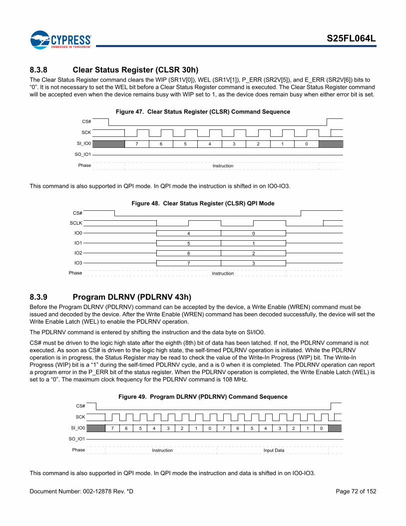
Document Number: 002-12878 Rev. *D Page 72 of 152
S25FL064L
8.3.8 Clear Status Register (CLSR 30h)The Clear Status Register command clears the WIP (SR1V[0]), WEL (SR1V[1]), P_ERR (SR2V[5]), and E_ERR (SR2V[6]) bits to “0”. It is not necessary to set the WEL bit before a Clear Status Register command is executed. The Clear Status Register command will be accepted even when the device remains busy with WIP set to 1, as the device does remain busy when either error bit is set.
Figure 47. Clear Status Register (CLSR) Command Sequence
This command is also supported in QPI mode. In QPI mode the instruction is shifted in on IO0-IO3.
Figure 48. Clear Status Register (CLSR) QPI Mode
8.3.9 Program DLRNV (PDLRNV 43h)Before the Program DLRNV (PDLRNV) command can be accepted by the device, a Write Enable (WREN) command must be issued and decoded by the device. After the Write Enable (WREN) command has been decoded successfully, the device will set the Write Enable Latch (WEL) to enable the PDLRNV operation.
The PDLRNV command is entered by shifting the instruction and the data byte on SI/IO0.
CS# must be driven to the logic high state after the eighth (8th) bit of data has been latched. If not, the PDLRNV command is not executed. As soon as CS# is driven to the logic high state, the self-timed PDLRNV operation is initiated. While the PDLRNV operation is in progress, the Status Register may be read to check the value of the Write-In Progress (WIP) bit. The Write-In Progress (WIP) bit is a “1” during the self-timed PDLRNV cycle, and a is 0 when it is completed. The PDLRNV operation can report a program error in the P_ERR bit of the status register. When the PDLRNV operation is completed, the Write Enable Latch (WEL) is set to a “0”. The maximum clock frequency for the PDLRNV command is 108 MHz.
Figure 49. Program DLRNV (PDLRNV) Command Sequence
This command is also supported in QPI mode. In QPI mode the instruction and data is shifted in on IO0-IO3.
CS#
SCK
SI_IO0
SO_IO1
Phase
7 6 5 4 3 2 1 0
Instruction
CS#
SCLK
IO0
IO1
IO2
IO3
Phase
4 0
5 1
6 2
7 3
Instruction
CS#
SCK
SI_IO0
SO_IO1
Phase
7 6 5 4 3 2 1 0 7 6 5 4 3 2 1 0
Instruction Input Data

Document Number: 002-12878 Rev. *D Page 73 of 152
S25FL064L
Figure 50. Program DLRNV (PDLRNV) Command Sequence – QPI Mode
8.3.10 Write DLRV (WDLRV 4Ah)Before the Write DLRV (WDLRV) command can be accepted by the device, a Write Enable (WREN) command must be issued and decoded by the device. After the Write Enable (WREN) command has been decoded successfully, the device will set the Write Enable Latch (WEL) to enable WDLRV operation.
The WDLRV command is entered by shifting the instruction and the data byte on SI/IO0.
CS# must be driven to the logic high state after the eighth (8th) bit of data has been latched. If not, the WDLRV command is not executed. As soon as CS# is driven to the logic high state, the WDLRV operation is initiated with no delays. The maximum clock frequency for the WDLRV command is 108 MHz.
Figure 51. Write DLRV (WDLRV) Command Sequence
This command is also supported in QPI mode. In QPI mode the instruction and data is shifted in on IO0-IO3.
Figure 52. Write DLRV (WDLRV) Command Sequence – QPI Mode
CS#
SCLK
IO0
IO1
IO2
IO3
Phase
4 0 4 0
5 1 5 1
6 2 6 2
7 3 7 3
Instruct. Input Data
CS#
SCK
SI_IO0
SO_IO1
Phase
7 6 5 4 3 2 1 0 7 6 5 4 3 2 1 0
Instruction Input Data
CS#
SCLK
IO0
IO1
IO2
IO3
Phase
4 0 4 0
5 1 5 1
6 2 6 2
7 3 7 3
Instruct. Input Data

Document Number: 002-12878 Rev. *D Page 74 of 152
S25FL064L
8.3.11 Data Learning Pattern Read (DLPRD 41h)The instruction 41h is shifted into SI/IO0 by the rising edge of the SCK signal followed by one dummy cycle. This latency period allows the device’s internal circuitry enough time to access data at the initial address. During latency cycles, the data value on IO0-IO3 are “don’t care” and may be high impedance. Then the 8-bit DLP is shifted out on SO/IO1. It is possible to read the DLP continuously by providing multiples of eight clock cycles. The maximum operating clock frequency for the DLPRD command is 108MHz.
Figure 53. DLP Read (DLPRD) Command Sequence
This command is also supported in QPI mode. In QPI mode the instruction is shifted in and returning data out on IO0-IO3.
Figure 54. DLP Read (DLPRD) Command Sequence – QPI Mode
8.3.12 Enter 4 Byte Address Mode (4BEN B7h)The enter 4 Byte Address Mode (4BEN) command sets the volatile Address Length status (ADS) bit (CR2V[0]) to 1 to change all 3 Byte address commands to require 4 Bytes of address. This command will not affect 4 Byte only commands which will still continue to expect 4 Bytes of address.
To return to 3 Byte Address mode the 4BEX command clears the volatile Address Length bit CR2V[0]=0). The WRAR command can also clear the volatile Address Length bit CR2V[0]=0). Also, a hardware or software reset may be used to return to the 3 byte address mode if the non-volatile Address Length bit CR2NV[1] = 0.
Figure 55. Enter 4 Byte Address Mode (4BEN B7h) Command Sequence
This command is also supported in QPI mode. In QPI mode the instruction is shifted in on IO0-IO3.
CS#
SCK
SI_IO0
SO_IO1
Phase
7 6 5 4 3 2 1 0
7 6 5 4 3 2 1 0 7 6 5 4 3 2 1 0
Instruction DY Register Read Repeat Register Read
CS#
SCLK
IO0
IO1
IO2
IO3
Phase
4 0 4 0 4 0
5 1 5 1 5 1
6 2 6 2 6 2
7 3 7 3 7 3
Instruct. Dummy Register Read Register Read
CS#
SCK
SI_IO0
SO_IO1
Phase
7 6 5 4 3 2 1 0
Instruction

Document Number: 002-12878 Rev. *D Page 75 of 152
S25FL064L
Figure 56. Enter 4 Byte Address QPI Mode
8.3.13 Exit 4 Byte Address Mode (4BEX E9h)The exit 4 Byte Address Mode (4BEX) command sets the volatile Address Length Status (ADS) bit (CR2V[0]) to 0 to change most 4 Byte address commands to require 3 Bytes of address. This command will not affect 4 Byte only commands which will still continue to expect 4 Bytes of address.
Figure 57. Exit 4 Byte Address Mode (4BEX E9h) Command Sequence
This command is also supported in QPI mode. In QPI mode the instruction is shifted in on IO0-IO3.
Figure 58. Exit 4 Byte Address QPI Mode
8.3.14 Read Any Register (RDAR 65h)The Read Any Register (RDAR) command provides a way to read device registers. The instruction is followed by a 3 or 4 Byte address (depending on the address length configuration CR2V[0]), followed by a number of latency (dummy) cycles set by CR3V[3:0]. Then the selected register contents are returned. If the read access is continued the same addressed register contents are returned until the command is terminated - only one register is read by each RDAR command.
Reading undefined locations provides undefined data.
The RDAR command may be used during embedded operations to read Status Register 1 (SR1V).
The RDAR command is not used for reading registers that act as a window into a larger array: IBLAR. There are separate commands required to select and read the location in the array accessed.
The RDAR command will read invalid data from the PASS register locations if the IRP Password protection mode is selected by programming IRP[2] to 0.
CS#
SCLK
IO0
IO1
IO2
IO3
Phase
4 0
5 1
6 2
7 3
Instruction
CS#
SCK
SI_IO0
SO_IO1
Phase
7 6 5 4 3 2 1 0
Instruction
CS#
SCLK
IO0
IO1
IO2
IO3
Phase
4 0
5 1
6 2
7 3
Instruction

Document Number: 002-12878 Rev. *D Page 76 of 152
S25FL064L
Figure 59. Read Any Register Read Command Sequence
Note:1. A = MSB of address = 23 for Address length CR2V[0] = 0, or 31 for CR2V[0]=1.
This command is also supported in QPI mode. In QPI mode the instruction and address is shifted in and returning data out on IO0-IO3.
Table 33. Register Address Map
Byte Address (Hex) Register Name Description
000000 SR1NV
Non-volatile Status and Configuration Registers Reading of Nov-volatile Status and Configuration Registers actually reads the volatile registers
000001 N/A
000002 CR1NV
000003 CR2NV
000004 CR3NV
000005 NVDLP
... N/A
000020 PASS[7:0]
Non-volatile Password Register
000021 PASS[15:8]
000022 PASS[23:16]
000023 PASS[31:24]
000024 PASS[39:32]
000025 PASS[47:40]
000026 PASS[55:48]
000027 PASS[63:56]
... N/A
000030 IRP[7:0] Non-volatile
000031 IRP[15:8]
... N/A
000039 PRPR[A15:A8] Pointer Region Protection Register A15:A8
00003A PRPR[A23:A16] Pointer Region Protection Register A23:A16
00003B N/A
... N/A
800000 SR1V
Volatile Status and Configuration Registers
800001 SR2V
800002 CR1V
800003 CR2V
800004 CR3V
800005 VDLP
... N/A
800040 PR Volatile Protection Register
... N/A
CS#
SCK
SI_IO0
SO_IO1
Phase
7 6 5 4 3 2 1 0 A 1 0
7 6 5 4 3 2 1 0
Instruction Address Dummy Cycles Data

Document Number: 002-12878 Rev. *D Page 77 of 152
S25FL064L
Figure 60. Read Any Register, QPI Mode, Command Sequence
Note:1. A = MSB of address = 23 for Address length CR2V[0] = 0, or 31 for CR2V[0]=1
8.3.15 Write Any Register (WRAR 71h)The Write Any Register (WRAR) command provides a way to write any device register - non-volatile or volatile. The instruction is followed by a 3 or 4 Byte address (depending on the address length configuration CR2V[0]), followed by one byte of data to write in the address selected register.
Before the WRAR command can be accepted by the device, a Write Enable (WREN) command must be issued and decoded by the device, which sets the Write Enable Latch (WEL) in the Status Register to enable any write operations. The WIP bit in SR1V may be checked to determine when the operation is completed. The P_ERR and E_ERR bits in SR2V may be checked to determine if any error occurred during the operation.
Some registers have a mixture of bit types and individual rules controlling which bits may be modified. Some bits are read only, some are OTP.
Read only bits are never modified and the related bits in the WRAR command data byte are ignored without setting a program or erase error indication (P_ERR or E_ERR in SR2V). Hence, the value of these bits in the WRAR data byte do not matter.
OTP bits may only be programmed to the level opposite of their default state. Writing of OTP bits back to their default state is ignored and no error is set.
Non-volatile bits which are changed by the WRAR data, require non-volatile register write time (tW) to be updated. The update process involves an erase and a program operation on the non-volatile register bits. If either the erase or program portion of the update fails the related error bit in SR2V and WIP in SR1V will be set to 1.
Volatile bits which are changed by the WRAR data, require the volatile register write time (tCS) to be updated.
Status Register 1 may be repeatedly read (polled) to monitor the Write-In-Progress (WIP) bit (SR1V[0]) to determine when the register write is completed and Status Register 1 for the error bits (SR2V[6,5]) to determine if there is write failure. If there is a write failure, the clear status command is used to clear the error status and enable the device to return to standby state. When the WRAR operation is completed, the Write Enable Latch (WEL) is set to a “0”
However, the PR register can not be written by the WRAR command. The PR register contents are treated as read only bits. Only the NVLOCK Bit Write (PRL) command can write the PR register.
The WRAR command to write the SR1NV, CR1NV CR2NV and CR3NV is protected from a hardware and software reset, the WRAR command to all other register are reset from a hardware or software reset.
The WRAR command sequence and behavior is the same as the PP or 4PP command with only a single byte of data provided. See Section 8.5.2, Page Program (PP 02h or 4PP 12H) on page 89.
The address map of the registers is the same as shown for Table 33, Register Address Map on page 76.
CS#
SCLK
IO0
IO1
IO2
IO3
Phase
4 0 A-3 4 0 4 0 4 0 4 0 4 0
5 1 A-2 5 1 5 1 5 1 5 1 5 1
6 2 A-1 6 2 6 2 6 2 6 2 6 2
7 3 A 7 3 7 3 7 3 7 3 7 3
Instruct. Address Dummy Data Data Data Data

Document Number: 002-12878 Rev. *D Page 78 of 152
S25FL064L
8.3.16 Set Burst Length (SBL 77h)The Set Burst Length (SBL) command is used to configure the Burst Wrap feature. Burst Wrap is used in conjunction with Quad I/O Read and DDR Quad I/O Read, in QIO or QPI modes, to access a fixed length and alignment of data. Certain applications can benefit from this feature by improving the overall system code execution performance. The Burst Wrap feature allows applications that use cache, to start filling a cache line with instruction or data from a critical address first, then fill the remainder of the cache line afterwards within a fixed length (8/16/32/64-bytes) of data, without issuing multiple read commands.
The Set Burst Length command is initiated by driving the CS# pin low and then shifting the instruction code “77h” followed by 24 dummy bits and 8 “Wrap Length Bits (WL[7]-WL[0])”. The command sequence is shown in Figure 61, Set Burst Length Command Sequence Quad I/O Mode on page 79 and Figure 62, Set Burst Length Command Sequence QPI Mode on page 79. Wrap Length bit WL[7] and the lower nibble WL[3:0] are not used. See Configuration Register 3 (CR3V[6:4]) for the encoding of WL[6]-WL[4] in Section 6.6.5, Configuration Register 3 on page 36.
Once WL[6:4] is set by a Set Burst Length command, all the following “Quad I/O Read” commands will use the WL[6:4] setting to access the 8/16/32/64-byte section of data. Note, Configuration Register 1 Quad bit CR1V[1] or Configuration Register 2 QPI bit CR2V[3] must be set to 1 in order to use the Quad I/O read and Set Burst Length commands. To exit the “Wrap Around” function and return to normal read operation, another Set Burst with Wrap command should be issued to set WL4 = 1. The default value of WL[6:4] upon power on, hardware or software reset as set in the CR2NV[6:4]. Use WRR or WRAR command to set the default wrap length in CR2NV[6;4].
The Set Burst Length (SBL) command writes only to CR3V[6:4] bits to enable or disable the wrapped read feature and set the wrap boundary. The SBL command cannot be used to set the read latency in CR3V[3:0]. The WRAR command must be used to set the read latency in CR3V or CR3NV.
See Table 34, Example Burst Wrap Sequences on page 78 for CR3V[6:5] values for wrap boundary's and start address. When enabled the wrapped read feature changes the related read commands from sequentially reading until the command ends, to reading sequentially wrapped within a group of bytes.
When the wrap mode is not enabled (Table 6.15 and Table 18), an unlimited length sequential read is performed.
When the wrap mode is enabled (Table 6.15 and Table 18) a fixed length and aligned group of 8, 16, 32, or 64 bytes is read starting at the byte address provided by the read command and wrapping around at the group alignment boundary.
The group of bytes is of length and aligned on an 8, 16, 32, or 64 byte boundary. CR3V[6:5] selects the boundary. See Section 6.6.5.2, Configuration Register 3 Volatile (CR3V) on page 40.
The starting address of the read command selects the group of bytes and the first data returned is the addressed byte. Bytes are then read sequentially until the end of the group boundary is reached. If the read continues the address wraps to the beginning of the group and continues to read sequentially. This wrapped read sequence continues until the command is ended by CS# returning high.
Table 34. Example Burst Wrap Sequences
CR3V Value (Hex)
Wrap Boundary (Bytes)
Start Address (Hex)
Address Sequence (Hex)
1X Sequential XXXXXX03 03, 04, 05, 06, 07, 08, 09, 0A, 0B, 0C, 0D, 0E, 0F, 10, 11, 12, 13, 14, 15, 16, 17, 18, ...
00 8 XXXXXX00 00, 01, 02, 03, 04, 05, 06, 07, 00, 01, 02, ...
00 8 XXXXXX07 07, 00, 01, 02, 03, 04, 05, 06, 07, 00, 01, ...
01 16 XXXXXX02 02, 03, 04, 05, 06, 07, 08, 09, 0A, 0B, 0C, 0D, 0E, 0F, 00, 01, 02, 03, ...
01 16 XXXXXX0C 0C, 0D, 0E, 0F, 00, 01, 02, 03, 02, 03, 04, 05, 06, 07, 08, 09, 0A, 0B, 0C, 0D, 0E, ...
02 32 XXXXXX0A0A, 0B, 0C, 0D, 0E, 0F, 10, 11, 12, 13, 14, 15, 16, 17, 18, 19, 1A, 1B, 1C, 1D, 1E, 1F, 00, 01, 02, 03, 04, 05, 06, 07, 08, 09, 0A, 0B, 0C, 0D, 0E, 0F, ...
02 32 XXXXXX1E1E, 1F, 00, 01, 02, 03, 04, 05, 06, 07, 08, 09, 0A, 0B, 0C, 0D, 0E, 0F, 10, 11, 12, 13, 14, 15,16, 17, 18, 19, 1A, 1B, 1C, 1D, 1E, 1F, 00, ...
03 64 XXXXXX0303, 04, 05, 06, 07, 08, 09, 0A, 0B, 0C, 0D, 0E, 0F, 10, 11, 12, 13, 14, 15, 16, 17, 18, 19, 1A, 1B, 1C, 1D, 1E, 1F, 20, 21, 22, 23, 24, 25, 26, 27, 28, 29, 2A, 2B, 2C, 2D, 2E, 2F, 30, 31, 32, 33, 34, 35, 36, 37, 38, 39, 3A, 3B, 3C, 3D, 3E, 3F, 00, 01, 02, ...
03 64 XXXXXX2E2E, 2F, 30, 31, 32, 33, 34, 35, 36, 37, 38, 39, 3A, 3B, 3C, 3D, 3E, 3F, 00, 01, 02, 03, 04, 05, 06, 07, 08, 09, 0A, 0B, 0C, 0D, 0E, 0F, 10, 11, 12, 13, 14, 15, 16, 17, 18, 19, 1A, 1B, 1C, 1D, 1E, 1F, 20, 21, 22, 23, 24, 25, 26, 27, 28, 29, 2A, 2B, 2C, 2D,, ...

Document Number: 002-12878 Rev. *D Page 79 of 152
S25FL064L
The power-on reset, hardware reset, or software reset default burst length can be changed by programming CR3NV with the desired value using the WRAR command.
Figure 61. Set Burst Length Command Sequence Quad I/O Mode
Figure 62. Set Burst Length Command Sequence QPI Mode
8.3.17 Enter QPI Mode (QPIEN 38h)The enter QPI Mode (QPIEN) command enables the QPI mode by setting the volatile QPI bit (CR2V[3]=1). See Table 14, Configuration Register 2 Volatile (CR2V) on page 35. The time required to enter QPI Mode is tQEN, see Table 53, SDR AC Characteristics on page 134, no other commands are allowed during the tQEN transition time to QPI mode.
To return to SPI mode the QPIEX command or a write to register (CR2V[3]=0) is required. A power on reset, hardware, or software reset will also return the part to SPI mode if the Non-volatile QPI (CR2NV[3]=0). See Table 12, Configuration Register 2 Non-volatile (CR2NV) on page 34.
Figure 63. Enter QPI Mode (QPIEN 38h) Command Sequence
CS
SCLK
IO0
IO1
IO2
IO3
Phase
7 6 5 4 3 2 1 0 X X X X X X WL4 X
X X X X X X WL5 X
X X X X X X WL6 X
X X X X X X X X
Instruction Don't Care Wrap
CS
SCLK
IO0
IO1
IO2
IO3
Phase
4 0 X X X X X X WL4 X
5 1 X X X X X X WL5 X
6 2 X X X X X X WL6 X
7 3 X X X X X X X X
Instruct. Don't Care Wrap
CS#
SCK
SI_IO0
SO_IO1
Phase
7 6 5 4 3 2 1 0
Instruction

Document Number: 002-12878 Rev. *D Page 80 of 152
S25FL064L
8.3.18 Exit QPI Mode (QPIEX F5h)The exit QPI Mode (QPIEX) command disables the QPI mode by setting the volatile QPI bit (CR2V[3]=0) and returning to SPI mode. See Table 14, Configuration Register 2 Volatile (CR2V) on page 35. The time required to exit QPI Mode is tQEX, see Table 53, SDR AC Characteristics on page 134, no other commands are allowed during the tQEX transition time to exit the QPI mode.
Figure 64. Exit QPI (QPIEX F5h) Command Sequence
8.4 Read Memory Array CommandsRead commands for the main Flash array provide many options for prior generation SPI compatibility or enhanced performance SPI:
Some commands transfer address or data on each rising edge of SCK. These are called Single Data Rate commands (SDR).
Some SDR commands transfer address one bit per falling edge of SCK and return data 1bit of data per rising edge of SCK. These are called Single width commands.
Some SDR commands transfer both address and data 2 or 4 bits per rising edge of SCK. These are called Dual I/O for 2 bit, Quad I/O, and QPI for 4 bit. QPI also transfers instructions 4 bits per rising edge.
Some commands transfer address and data on both the rising edge and falling edge of SCK. These are called Double Data Rate (DDR) commands.
There are DDR commands for 4 bits of address or data per SCK edge. These are called Quad I/O DDR and QPI DDR for 4 bit per edge transfer.
All of these commands, except QPI Read, begin with an instruction code that is transferred one bit per SCK rising edge. QPI Read transfers the instruction 4 bits per SCK rising edge.The instruction is followed by either a 3 or 4 byte address transferred at SDR or DDR. Commands transferring address or data 2 or 4 bits per clock edge are called Multiple I/O (MIO) commands. For FL-L family devices at 256Mb or higher density, the traditional SPI 3 byte addresses are unable to directly address all locations in the memory array. Separate 4 Byte address read commands are provided for access to the entire address space. These devices may be configured to take a 4 byte address from the host system with the traditional 3 byte address commands. The 4 byte address mode for traditional commands is activated by setting the Address Length bit in configuration register 2 to “1”. In the S25FL128L higher order address bits above A22 in the 4 byte address commands, or commands using 4 Byte Address mode are not relevant and are ignored because the Flash array is only 64Mb in size.
The Dual I/O, Quad I/O and QPI commands provide a performance improvement option controlled by mode bits that are sent following the address bits. The mode bits indicate whether the command following the end of the current read will be another read of the same type, without an instruction at the beginning of the read. These mode bits give the option to eliminate the instruction cycles when doing a series of Dual or Quad read accesses.
Some commands require delay cycles following the address or mode bits to allow time to access the memory array - read latency. The delay or read latency cycles are traditionally called dummy cycles. The dummy cycles are ignored by the memory thus any data provided by the host during these cycles is “don’t care” and the host may also leave the SI signal at high impedance during the dummy cycles. When MIO commands are used the host must stop driving the IO signals (outputs are high impedance) before the end of last dummy cycle. When DDR commands are used the host must not drive the I/O signals during any dummy cycle. The number of dummy cycles varies with the SCK frequency or performance option selected via the Configuration Register 2 (CR3V[3:0]) Latency Code. Dummy cycles are measured from SCK falling edge to next SCK falling edge. SPI outputs are traditionally driven to a new value on the falling edge of each SCK. Zero dummy cycles means the returning data is driven by the memory on the same falling edge of SCK that the host stops driving address or mode bits.
CS#
SCLK
IO0
IO1
IO2
IO3
Phase
4 0
5 1
6 2
7 3
Instruction

Document Number: 002-12878 Rev. *D Page 81 of 152
S25FL064L
The DDR commands may optionally have an 8 edge Data Learning Pattern (DLP) driven by the memory, on all data outputs, in the dummy cycles immediately before the start of data. The DLP can help the host memory controller determine the phase shift from SCK to data edges so that the memory controller can capture data at the center of the data eye.
When using SDR I/O commands at higher SCK frequencies (>50 MHz), an LC that provides 1 or more dummy cycles should be selected to allow additional time for the host to stop driving before the memory starts driving data, to minimize I/O driver conflict. When using DDR I/O commands with the DLP enabled, an LC that provides 5 or more dummy cycles should be selected to allow 1 cycle of additional time for the host to stop driving before the memory starts driving the 4 cycle DLP.
Each read command ends when CS# is returned High at any point during data return. CS# must not be returned High during the mode or dummy cycles before data returns as this may cause mode bits to be captured incorrectly; making it indeterminate as to whether the device remains in continuous read mode.
8.4.1 Read (Read 03h or 4READ 13h)The instruction
03h (CR2V[0]=0) is followed by a 3-byte address (A23-A0) or
03h (CR2V[0]=1) is followed by a 4-byte address (A31-A0) or
13h is followed by a 4-byte address (A31-A0)
Then the memory contents, at the address given, are shifted out on SO/IO1.
The address can start at any byte location of the memory array. The address is automatically incremented to the next higher address in sequential order after each byte of data is shifted out. The entire memory can therefore be read out with one single read instruction and address 000000h provided. When the highest address is reached, the address counter will wrap around and roll back to 000000h, allowing the read sequence to be continued indefinitely.
Figure 65. Read Command Sequence
Note:1. A = MSB of address = 23 for CR2V[0]=0, or 31 for CR2V[0]=1 or command 13h.
8.4.2 Fast Read (FAST_READ 0Bh or 4FAST_READ 0Ch)The instruction
0Bh (CR2V[0]=0) is followed by a 3-byte address (A23-A0) or
0Bh (CR2V[0]=1) is followed by a 4-byte address (A31-A0) or
0Ch is followed by a 4-byte address (A31-A0)
The address is followed by dummy cycles depending on the latency code set in the Configuration Register CR3V[3:0]. The dummy cycles allow the device internal circuits additional time for accessing the initial address location. During the dummy cycles the data value on SO/IO1 is “don’t care” and may be high impedance. Then the memory contents, at the address given, are shifted out on SO/IO1.
The address can start at any byte location of the memory array. The address is automatically incremented to the next higher address in sequential order after each byte of data is shifted out. The entire memory can therefore be read out with one single read instruction and address 000000h provided. When the highest address is reached, the address counter will wrap around and roll back to 000000h, allowing the read sequence to be continued indefinitely.
CS#
SCK
SI_IO0
SO_IO1
Phase
7 6 5 4 3 2 1 0 A 1 0
7 6 5 4 3 2 1 0 7 6 5 4 3 2 1 0
Instruction Address Data 1 Data N

Document Number: 002-12878 Rev. *D Page 82 of 152
S25FL064L
Figure 66. Fast Read (FAST_READ) Command Sequence
Note:1. A = MSB of address = 23 for CR2V[0]=0, or 31 for CR2V[0]=1 or command 0Ch.
8.4.3 Dual Output Read (DOR 3Bh or 4DOR 3Ch)The instruction
3Bh (CR2V[0]=0) is followed by a 3-byte address (A23-A0) or
3Bh (CR2V[0]=1) is followed by a 4-byte address (A31-A0) or
3Ch is followed by a 4-byte address (A31-A0)
The address is followed by dummy cycles depending on the latency code set in the Configuration Register CR3V[3:0]. The dummy cycles allow the device internal circuits additional time for accessing the initial address location. During the dummy cycles the data value on IO0 (SI) and IO1 (S0) is “don’t care” and may be high impedance.
Then the memory contents, at the address given, is shifted out two bits at a time through IO0 (SI) and IO1 (SO). Two bits are shifted out at the SCK frequency by the falling edge of the SCK signal.
The address can start at any byte location of the memory array. The address is automatically incremented to the next higher address in sequential order after each byte of data is shifted out. The entire memory can therefore be read out with one single read instruction and address 000000h provided. When the highest address is reached, the address counter will wrap around and roll back to 000000h, allowing the read sequence to be continued indefinitely.
For Dual Output Read commands, there are dummy cycles required after the last address bit is shifted into IO0 (SI) before data begins shifting out of IO0 and IO1.
Figure 67. Dual Output Read Command Sequence
Note:1. A = MSB of address = 23 for CR2V[0]=0, or 31 for CR2V[0]=1 or command 3Ch.
CS#
SCK
SI_IO0
SO_IO1
IO2-IO3
Phase
7 6 5 4 3 2 1 0 A 1 0
7 6 5 4 3 2 1 0
Instruction Address Dummy Cycles Data 1
CS#
SCK
IO0
IO1
Phase
7 6 5 4 3 2 1 0 A 1 0 6 4 2 0 6 4 2 0
7 5 3 1 7 5 3 1
Instruction Address Dummy Cycles Data 1 Data 2

Document Number: 002-12878 Rev. *D Page 83 of 152
S25FL064L
8.4.4 Quad Output Read (QOR 6Bh or 4QOR 6Ch)The instruction
6Bh (CR2V[0]=0) is followed by a 3-byte address (A23-A0) or
6Bh (CR2V[0]=1) is followed by a 4-byte address (A31-A0) or
6Ch is followed by a 4-byte address (A31-A0)
The address is followed by dummy cycles depending on the latency code set in the Configuration Register CR3V[3:0]. The dummy cycles allow the device internal circuits additional time for accessing the initial address location. During the dummy cycles the data value on IO0 - IO3 is “don’t care” and may be high impedance.
Then the memory contents, at the address given, is shifted out four bits at a time through IO0 - IO3. Each nibble (4 bits) is shifted out at the SCK frequency by the falling edge of the SCK signal.
The address can start at any byte location of the memory array. The address is automatically incremented to the next higher address in sequential order after each byte of data is shifted out. The entire memory can therefore be read out with one single read instruction and address 000000h provided. When the highest address is reached, the address counter will wrap around and roll back to 000000h, allowing the read sequence to be continued indefinitely.
For Quad Output Read commands, there are dummy cycles required after the last address bit is shifted into IO0 before data begins shifting out of IO0 - IO3.
Figure 68. Quad Output Read Command Sequence
Note:1. A = MSB of address = 23 for CR2V[0]=0, or 31 for CR2V[0]=1 or command 6Ch.
8.4.5 Dual I/O Read (DIOR BBh or 4DIOR BCh)The instruction
BBh (CR2V[0]=0) is followed by a 3-byte address (A23-A0) or
BBh (CR2V[0]=1) is followed by a 4-byte address (A31-A0) or
BCh is followed by a 4-byte address (A31-A0)
The Dual I/O Read commands improve throughput with two I/O signals — IO0 (SI) and IO1 (SO). This command takes input of the address and returns read data two bits per SCK rising edge. In some applications, the reduced address input and data output time might allow for code execution in place (XIP) i.e. directly from the memory device.
The Dual I/O Read command has continuous read mode bits that follow the address so, a series of Dual I/O Read commands may eliminate the 8 bit instruction after the first Dual I/O Read command sends a mode bit pattern of Axh that indicates the following command will also be a Dual I/O Read command. The first Dual I/O Read command in a series starts with the 8 bit instruction, followed by address, followed by four cycles of mode bits, followed by an optional latency period. If the mode bit pattern is Axh the next command is assumed to be an additional Dual I/O Read command that does not provide instruction bits. That command starts with address, followed by mode bits, followed by optional latency.
Variable latency may be added after the mode bits are shifted into SI and SO before data begins shifting out of IO0 and IO1. This latency period (dummy cycles) allows the device internal circuitry enough time to access data at the initial address. During the dummy cycles, the data value on SI and SO are “don’t care” and may be high impedance. The number of dummy cycles is determined by the frequency of SCK. The latency is configured in CR3V[3:0].
CS#
SCK
IO0
IO1
IO2
IO3
Phase
7 6 5 4 3 2 1 0 A 1 0 4 0 4 0 4 0 4 0 4 0 4
5 1 5 1 5 1 5 1 5 1 5
6 2 6 2 6 2 6 2 6 2 6
7 3 7 3 7 3 7 3 7 3 7
Instruction Address Dummy D1 D2 D3 D4 D5
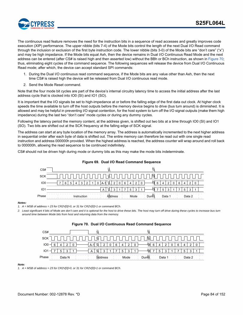
Document Number: 002-12878 Rev. *D Page 84 of 152
S25FL064L
The continuous read feature removes the need for the instruction bits in a sequence of read accesses and greatly improves code execution (XIP) performance. The upper nibble (bits 7-4) of the Mode bits control the length of the next Dual I/O Read command through the inclusion or exclusion of the first byte instruction code. The lower nibble (bits 3-0) of the Mode bits are “don’t care” (“x”) and may be high impedance. If the Mode bits equal Axh, then the device remains in Dual I/O Continuous Read Mode and the next address can be entered (after CS# is raised high and then asserted low) without the BBh or BCh instruction, as shown in Figure 70; thus, eliminating eight cycles of the command sequence. The following sequences will release the device from Dual I/O Continuous Read mode; after which, the device can accept standard SPI commands:
1. During the Dual I/O continuous read command sequence, if the Mode bits are any value other than Axh, then the next time CS# is raised high the device will be released from Dual I/O continuous read mode.
2. Send the Mode Reset command.
Note that the four mode bit cycles are part of the device’s internal circuitry latency time to access the initial address after the last address cycle that is clocked into IO0 (SI) and IO1 (SO).
It is important that the I/O signals be set to high-impedance at or before the falling edge of the first data out clock. At higher clock speeds the time available to turn off the host outputs before the memory device begins to drive (bus turn around) is diminished. It is allowed and may be helpful in preventing I/O signal contention, for the host system to turn off the I/O signal outputs (make them high impedance) during the last two “don’t care” mode cycles or during any dummy cycles.
Following the latency period the memory content, at the address given, is shifted out two bits at a time through IO0 (SI) and IO1 (SO). Two bits are shifted out at the SCK frequency at the falling edge of SCK signal.
The address can start at any byte location of the memory array. The address is automatically incremented to the next higher address in sequential order after each byte of data is shifted out. The entire memory can therefore be read out with one single read instruction and address 000000h provided. When the highest address is reached, the address counter will wrap around and roll back to 000000h, allowing the read sequence to be continued indefinitely.
CS# should not be driven high during mode or dummy bits as this may make the mode bits indeterminate.
Figure 69. Dual I/O Read Command Sequence
Notes:1. A = MSB of address = 23 for CR2V[0]=0, or 31 for CR2V[0]=1 or command BCh.
2. Least significant 4 bits of Mode are don’t care and it is optional for the host to drive these bits. The host may turn off drive during these cycles to increase bus turn around time between Mode bits from host and returning data from the memory.
Figure 70. Dual I/O Continuous Read Command Sequence
Note:1. A = MSB of address = 23 for CR2V[0]=0, or 31 for CR2V[0]=1 or command BCh.
CS#
SCK
IO0
IO1
Phase
7 6 5 4 3 2 1 0 A-1 2 0 6 4 2 0 6 4 2 0 6 4 2 0
A 3 1 7 5 3 1 7 5 3 1 7 5 3 1
Instruction Address Mode Dum Data 1 Data 2
CS#
SCK
IO0
IO1
Phase
6 4 2 0 A-1 2 0 6 4 2 0 6 4 2 0 6 4 2 0
7 5 3 1 A 3 1 7 5 3 1 7 5 3 1 7 5 3 1
Data N Address Mode Dum Data 1 Data 2

Document Number: 002-12878 Rev. *D Page 85 of 152
S25FL064L
8.4.6 Quad I/O Read (QIOR EBh or 4QIOR ECh)The instruction,
EBh (CR2V[0]=0) is followed by a 3-byte address (A23-A0) or
EBh (CR2V[0]=1) is followed by a 4-byte address (A31-A0) or
ECh is followed by a 4-byte address (A31-A0)
The Quad I/O Read command improves throughput with four I/O signals IO0-IO3. It allows input of the address bits four bits per serial SCK clock. In some applications, the reduced instruction overhead might allow for code execution (XIP) directly from FL-L family devices. The QUAD bit of the Configuration Register 1 must be set (CR1V[1]=1) or the QPI bit of Configuration Register 2 must be set (CR2V[1]=1 to enable the Quad capability of FL-L family devices.
For the Quad I/O Read command, there is a latency required after the mode bits (described below) before data begins shifting out of IO0-IO3. This latency period (i.e., dummy cycles) allows the device’s internal circuitry enough time to access data at the initial address. During latency cycles, the data value on IO0-IO3 are “don’t care” and may be high impedance. The number of dummy cycles is determined by the frequency of SCK. The latency is configured in CR3V[3:0].
Following the latency period, the memory contents at the address given, is shifted out four bits at a time through IO0-IO3. Each nibble (4 bits) is shifted out at the SCK frequency by the falling edge of the SCK signal.
The address can start at any byte location of the memory array. The address is automatically incremented to the next higher address in sequential order after each byte of data is shifted out. The entire memory can therefore be read out with one single read instruction and address 000000h provided. When the highest address is reached, the address counter will wrap around and roll back to 000000h, allowing the read sequence to be continued indefinitely.
Address jumps can be done without the need for additional Quad I/O Read instructions. This is controlled through the setting of the Mode bits (after the address sequence, as shown in Figure 71 on page 86. This added feature removes the need for the instruction sequence and greatly improves code execution (XIP). The upper nibble (bits 7-4) of the Mode bits control the length of the next Quad I/O instruction through the inclusion or exclusion of the first byte instruction code. The lower nibble (bits 3-0) of the Mode bits are “don’t care” (“x”). If the Mode bits equal Axh, then the device remains in Quad I/O High Performance Read Mode and the next address can be entered (after CS# is raised high and then asserted low) without requiring the EBh or ECh instruction, as shown in Figure 73 on page 86; thus, eliminating eight cycles for the command sequence. The following sequences will release the device from Quad I/O High Performance Read mode; after which, the device can accept standard SPI commands:
1. During the Quad I/O Read Command Sequence, if the Mode bits are any value other than Axh, then the next time CS# is raised high the device will be released from Quad I/O High Performance Read mode.
2. Send the Mode Reset command.
Note that the two mode bit clock cycles and additional wait states (i.e., dummy cycles) allow the device’s internal circuitry latency time to access the initial address after the last address cycle that is clocked into IO0-IO3.
It is important that the IO0-IO3 signals be set to high-impedance at or before the falling edge of the first data out clock. At higher clock speeds the time available to turn off the host outputs before the memory device begins to drive (bus turn around) is diminished. It is allowed and may be helpful in preventing IO0-IO3 signal contention, for the host system to turn off the IO0-IO3 signal outputs (make them high impedance) during the last “don’t care” mode cycle or during any dummy cycles.
CS# should not be driven high during mode or dummy bits as this may make the mode bits indeterminate.
In QPI mode (CR2V[3]=1) the Quad I/O instructions are sent 4 bits per SCK rising edge. The remainder of the command protocol is identical to the Quad I/O commands.

Document Number: 002-12878 Rev. *D Page 86 of 152
S25FL064L
Figure 71. Quad I/O Read Initial Access Command Sequence
Note:1. A = MSB of address = 23 for CR2V[0]=0, or 31 for CR2V[0]=1 or command ECh.
Figure 72. Quad I/O Read Initial Access Command Sequence QPI mode
Note:1. A = MSB of address = 23 for CR2V[0]=0, or 31 for CR2V[0]=1 or command ECh.
Figure 73. Continuous Quad I/O Read Command Sequence
Notes:1. A = MSB of address = 23 for CR2V[0]=0, or 31 for CR2V[0]=1 or command ECh.
2. The same sequence is used in QPI mode.
CS#
SCLK
IO0
IO1
IO2
IO3
Phase
7 6 5 4 3 2 1 0 A-3 4 0 4 0 4 0 4 0 4 0 4 0
A-2 5 1 5 1 5 1 5 1 5 1 5 1
A-1 6 2 6 2 6 2 6 2 6 2 6 2
A 7 3 7 3 7 3 7 3 7 3 7 3
Instruction Address Mode Dummy D1 D2 D3 D4
CS#
SCLK
IO0
IO1
IO2
IO3
Phase
4 0 A-3 4 0 4 0 4 0 4 0 4 0 4 0
5 1 A-2 5 1 5 1 5 1 5 1 5 1 5 1
6 2 A-1 6 2 6 2 6 2 6 2 6 2 6 2
7 3 A 7 3 7 3 7 3 7 3 7 3 7 3
Instruct. Address Mode Dummy D1 D2 D3 D4
CS#
SCK
IO0
IO1
IO2
IO3
Phase
4 0 4 0 A-3 4 0 4 0 4 0 4 0 6 4 2 0
5 1 5 1 A-2 5 1 5 1 5 1 5 1 7 5 3 1
6 2 6 2 A-1 6 2 6 2 6 2 6 1 7 5 3 1
7 3 7 3 A 7 3 7 3 7 3 7 1 7 5 3 1
DN-1 DN Address Mode Dummy D1 D2 D3 D4
Document Number: 002-12878 Rev. *D Page 87 of 152
S25FL064L
8.4.7 DDR Quad I/O Read (EDh, EEh)The DDR Quad I/O Read command improves throughput with four I/O signals IO0-IO3. It is similar to the Quad I/O Read command but allows input of the address four bits on every edge of the clock. In some applications, the reduced instruction overhead might allow for code execution (XIP) directly from FL-L Family devices. The QUAD bit of the Configuration Register 1 must be set (CR1V[1]=1) or the QPI bit of Configuration Register 2 must be set (CR2V[1]=1 to enable the Quad capability of FL-L family devices.
The instruction
EDh (CR2V[0]=0) is followed by a 3-byte address (A23-A0) or
EDh (CR2V[0]=1) is followed by a 4-byte address (A31-A0) or
EEh is followed by a 4-byte address (A31-A0)
The address is followed by mode bits. Then the memory contents, at the address given, is shifted out, in a DDR fashion, with four bits at a time on each clock edge through IO0-IO3.
The maximum operating clock frequency for DDR Quad I/O Read command is 54 MHz.
For DDR Quad I/O Read, there is a latency required after the last address and mode bits are shifted into the IO0-IO3 signals before data begins shifting out of IO0-IO3. This latency period (dummy cycles) allows the device’s internal circuitry enough time to access the initial address. During these latency cycles, the data value on IO0-IO3 are “don’t care” and may be high impedance. When the Data Learning Pattern (DLP) is enabled the host system must not drive the IO signals during the dummy cycles. The IO signals must be left high impedance by the host so that the memory device can drive the DLP during the dummy cycles.
The number of dummy cycles is determined by the frequency of SCK. The latency is configured in CR3V[3:0].
Mode bits allow a series of Quad I/O DDR commands to eliminate the 8 bit instruction after the first command sends a complementary mode bit pattern. This feature removes the need for the eight bit SDR instruction sequence and dramatically reduces initial access times (improves XIP performance). The Mode bits control the length of the next DDR Quad I/O Read operation through the inclusion or exclusion of the first byte instruction code. If the upper nibble (IO[7:4]) and lower nibble (IO[3:0]) of the Mode bits are complementary (i.e. 5h and Ah) the device transitions to Continuous DDR Quad I/O Read Mode and the next address can be entered (after CS# is raised high and then asserted low) without requiring the EDh or EEh instruction, thus eliminating eight cycles from the command sequence. The following sequences will release the device from Continuous DDR Quad I/O Read mode; after which, the device can accept standard SPI commands:
1. During the DDR Quad I/O Read Command Sequence, if the Mode bits are not complementary the next time CS# is raised high and then asserted low the device will be released from DDR Quad I/O Read mode.
2. Send the Mode Reset command.
The address can start at any byte location of the memory array. The address is automatically incremented to the next higher address in sequential order after each byte of data is shifted out. The entire memory can therefore be read out with one single read instruction and address 000000h provided. When the highest address is reached, the address counter will wrap around and roll back to 000000h, allowing the read sequence to be continued indefinitely.
CS# should not be driven high during mode or dummy bits as this may make the mode bits indeterminate. Note that the memory devices may drive the IOs with a preamble prior to the first data value. The preamble is a Data Learning Pattern (DLP) that is used by the host controller to optimize data capture at higher frequencies. The preamble drives the IO bus for the four clock cycles immediately before data is output. The host must be sure to stop driving the IO bus prior to the time that the memory starts outputting the preamble.
The preamble is intended to give the host controller an indication about the round trip time from when the host drives a clock edge to when the corresponding data value returns from the memory device. The host controller will skew the data capture point during the preamble period to optimize timing margins and then use the same skew time to capture the data during the rest of the read operation. The optimized capture point will be determined during the preamble period of every read operation. This optimization strategy is intended to compensate for both the PVT (process, voltage, temperature) of both the memory device and the host controller as well as any system level delays caused by flight time on the PCB.

Document Number: 002-12878 Rev. *D Page 88 of 152
S25FL064L
Although the data learning pattern (DLP) is programmable, the following example shows example of the DLP of 34h. The DLP 34h (or 00110100) will be driven on each of the active outputs (i.e. all four IOs). This pattern was chosen to cover both “DC” and “AC” data transition scenarios. The two DC transition scenarios include data low for a long period of time (two half clocks) followed by a high going transition (001) and the complementary low going transition (110). The two AC transition scenarios include data low for a short period of time (one half clock) followed by a high going transition (101) and the complementary low going transition (010). The DC transitions will typically occur with a starting point closer to the supply rail than the AC transitions that may not have fully settled to their steady state (DC) levels. In many cases the DC transitions will bound the beginning of the data valid period and the AC transitions will bound the ending of the data valid period. These transitions will allow the host controller to identify the beginning and ending of the valid data eye. Once the data eye has been characterized the optimal data capture point can be chosen. See Section 6.6.11, DDR Data Learning Registers on page 44 for more details.
In QPI mode (CR2V[3]=1) the DDR Quad I/O instructions are sent 4 bits at SCK rising edge. The remainder of the command protocol is identical to the DDR Quad I/O commands.
Figure 74. DDR Quad I/O Read Initial Access
Notes:1. A = MSB of address = 23 for CR2V[0]=0, or 31 for CR2V[0]=1 or command EEh
2. Example DLP of 34h (or 00110100)
Figure 75. DDR Quad I/O Read Initial Access QPI Mode
Notes: 1. A = MSB of address = 23 for CR2V[0]=0, or 31 for CR2V[0]=1 or command EEh.
2. Example DLP of 34h (or 00110100).
Figure 76. Continuous DDR Quad I/O Read Subsequent Access
Notes: 1. A = MSB of address = 23 for CR2V[0]=0, or 31 for CR2V[0]=1 or command EEh.
2. The same sequence is used in QPI mode.
3. Example DLP of 34h (or 00110100).
CS#
SCK
IO0
IO1
IO2
IO3
Phase
7 6 5 4 3 2 1 0 A-3 8 4 0 4 0 7 6 5 4 3 2 1 0 4 0 4 0
A-2 9 5 1 5 1 7 6 5 4 3 2 1 0 5 1 5 1
A-1 10 6 2 6 2 7 6 5 4 3 2 1 0 6 2 6 2
A 11 7 3 7 3 7 6 5 4 3 2 1 0 7 3 7 3
Instruction Address Mode Dummy DLP D1 D2
CS#
SCLK
IO0
IO1
IO2
IO3
Phase
4 0 A-3 8 4 0 4 0 7 6 5 4 3 2 1 0 4 0 4 0
5 1 A-2 9 5 1 5 1 7 6 5 4 3 2 1 0 5 1 5 1
6 2 A-1 10 6 2 6 2 7 6 5 4 3 2 1 0 6 2 6 2
7 3 A 11 7 3 7 3 7 6 5 4 3 2 1 0 7 3 7 3
Instruct. Address Mode Dummy DLP D1 D2
CS#
SCK
IO0
IO1
IO2
IO3
Phase
A-3 8 4 0 4 0 7 6 5 4 3 2 1 0 4 0 4 0
A-2 9 5 1 5 1 7 6 5 4 3 2 1 0 5 1 5 1
A-1 10 6 2 6 2 7 6 5 4 3 2 1 0 6 2 6 2
A 11 7 3 7 3 7 6 5 4 3 2 1 0 7 3 7 3
Address Mode Dummy DLP D1 D2

Document Number: 002-12878 Rev. *D Page 89 of 152
S25FL064L
8.5 Program Flash Array Commands
8.5.1 Program Granularity
8.5.1.1 Page ProgrammingPage Programming is done by loading a Page Buffer with data to be programmed and issuing a programming command to move data from the buffer to the memory array. This sets an upper limit on the amount of data that can be programmed with a single programming command. Page Programming allows up to a page size 256bytes to be programmed in one operation. The page is aligned on the page size address boundary. It is possible to program from one bit up to a page size in each Page programming operation. For the very best performance, programming should be done in full pages of 256bytes aligned on 256byte boundaries with each Page being programmed only once.
8.5.1.2 Single Byte ProgrammingSingle Byte Programming allows full backward compatibility to the legacy standard SPI Page Programming (PP) command by allowing a single byte to be programmed anywhere in the memory array.
8.5.2 Page Program (PP 02h or 4PP 12H)The Page Program (PP) command allows bytes to be programmed in the memory (changing bits from 1 to 0). Before the Page Program (PP) commands can be accepted by the device, a Write Enable (WREN) command must be issued and decoded by the device. After the Write Enable (WREN) command has been decoded successfully, the device sets the Write Enable Latch (WEL) in the Status Register to enable any write operations.
The instruction
02h (CR2V[0]=0) is followed by a 3-byte address (A23-A0) or
02h (CR2V[0]=1) is followed by a 4-byte address (A31-A0) or
12h is followed by a 4-byte address (A31-A0)
and at least one data byte on SI/IO0. Up to a page can be provided on SI/IO0 after the 3-byte address with instruction 02h or 4-byte address with instruction 12h has been provided. As with the write and erase commands, the CS# pin must be driven high after the eighth bit of the last byte has been latched. If this is not done the Page Program command will not be executed. After CS# is driven high, the self-timed Page Program command will commence for a time duration of tPP.
Using the Page Program (PP) command to load an entire page, within the page boundary, will save overall programming time versus loading less than a page into the program buffer.
The programming process is managed by the Flash memory device internal control logic. After a programming command is issued, the programming operation status can be checked using the Read Status Register 1 command. The WIP bit (SR1V[0]) will indicate when the programming operation is completed. The P_ERR bit (SR2V[5]) will indicate if an error occurs in the programming operation that prevents successful completion of programming. This includes attempted programming of a protected area.
Figure 77. Page Program (PP 02h or 4PP 12h) Command Sequence
Note:1. A = MSB of address = A23 for PP 02h with CR2V[0]=0, or A31 for PP 02h with CR2V[0]=1, or for 4PP 12h.
This command is also supported in QPI mode. In QPI mode the instruction, address and data is shifted in on IO0-IO3.
CS#
SCK
SI_IO0
SO_IO1
Phase
7 6 5 4 3 2 1 0 A 5 4 3 2 1 0 7 6 5 4 3 2 1 0 7 6 5 4 3 2 1 0
Instruction Address Input Data 1 Input Data 2

Document Number: 002-12878 Rev. *D Page 90 of 152
S25FL064L
Figure 78. Page Program (PP 02h or 4PP 12h) QPI Mode Command Sequence
Note:1. A = MSB of address = A23 for PP 02h with CR2V[0]=0, or A31 for PP 02h with CR2V[0]=1, or for 4PP 12h.
8.5.3 Quad Page Program (QPP 32h or 4QPP 34h)The Quad-input Page Program (QPP) command allows bytes to be programmed in the memory (changing bits from 1 to 0). The Quad-input Page Program (QPP) command allows up to a page of data to be loaded into the Page Buffer using four signals: IO0-IO3. QPP can improve performance for PROM Programmer and applications that have slower clock speeds (< 12 MHz) by loading 4 bits of data per clock cycle. Systems with faster clock speeds do not realize as much benefit for the QPP command since the inherent page program time becomes greater than the time it takes to clock-in the data. The maximum frequency for the QPP command is 108MHz.
To use Quad Page Program the Quad Enable Bit in the Configuration Register must be set (QUAD=1). A Write Enable command must be executed before the device will accept the QPP command (Status Register 1, WEL=1).
The instruction
32h (CR2V[0]=0) is followed by a 3-byte address (A23-A0) or
32h (CR2V[0]=1) is followed by a 4-byte address (A31-A0) or
34h is followed by a 4-byte address (A31-A0)
and at least one data byte, into the IO signals. Data must be programmed at previously erased (FFh) memory locations.
All other functions of QPP are identical to Page Program. The QPP command sequence is shown in the figure below.
Figure 79. Quad Page Program Command Sequence
Note:1. A = MSB of address = A23 for QPP 32h with CR2V[0]=0, or A31 for QPP 32h with CR2V[0]=1, or for 4QPP 34h.
CS#
SCLK
IO0
IO1
IO2
IO3
Phase
4 0 A-3 4 0 4 0 4 0 4 0 4 0
5 1 A-2 5 1 5 1 5 1 5 1 5 1
6 2 A-1 6 2 6 2 6 2 6 2 6 2
7 3 A 7 3 7 3 7 3 7 3 7 3
Instruct. Address Input D1 Input D2 Input D3 Input D4
CS#
SCK
IO0
IO1
IO2
IO3
Phase
7 6 5 4 3 2 1 0 A 1 0 4 0 4 0 4 0 4 0 4 0 4
5 1 5 1 5 1 5 1 5 1 5
6 2 6 2 6 2 6 2 6 2 6
7 3 7 3 7 3 7 3 7 3 7
Instruction Address Data 1 Data 2 Data 3 Data 4 Data 5 ...

Document Number: 002-12878 Rev. *D Page 91 of 152
S25FL064L
8.6 Erase Flash Array Commands
8.6.1 Sector Erase (SE 20h or 4SE 21h)The Sector Erase (SE) command sets all bits in the addressed sector to 1 (all bytes are FFh). Before the Sector Erase (SE) command can be accepted by the device, a Write Enable (WREN) command must be issued and decoded by the device, which sets the Write Enable Latch (WEL) in the Status Register to enable any write operations.
The instruction
20h [CR2V[0]=0] is followed by a 3-byte address (A23-A0), or
20h [CR2V[0]=1] is followed by a 4-byte address (A31-A0), or
21h is followed by a 4-byte address (A31-A0)
CS# must be driven into the logic high state after the twenty-fourth or thirty-second bit of the address has been latched in on SI/IO0. This will initiate the beginning of internal erase cycle, which involves the pre-programming and erase of the chosen sector of the flash memory array. If CS# is not driven high after the last bit of address, the sector erase operation will not be executed.
As soon as CS# is driven high, the internal erase cycle will be initiated. With the internal erase cycle in progress, the user can read the value of the Write-In Progress (WIP) bit to determine when the operation has been completed. The WIP bit will indicate a “1”. when the erase cycle is in progress and a “0” when the erase cycle has been completed.
A SE or 4SE command applied to a sector that has been write protected through the Legacy Block Protection, Individual Block Lock or Pointer Region Protection will not be executed and will set the E_ERR status.
Figure 80. Sector Erase (SE 20h or 4SE 21h) Command Sequence
Note:1. A = MSB of address = A23 for SE 20h with CR2V[0]=0, or A31 for SE 20h with CR2V[0]=1 or for 4SE 21h.
This command is also supported in QPI mode. In QPI mode the instruction and address is shifted in on IO0-IO3.
Figure 81. Sector Erase (SE 20h or 4SE 21h) QPI Mode Command Sequence
Note:1. A = MSB of address = A23 for SE 20h with CR2V[0]=0, or A31 for SE 20h with CR2V[0]=1 or for 4SE 21h.
CS#
SCK
SI_IO0
SO_IO1
Phase
7 6 5 4 3 2 1 0 A 1 0
Instruction Address
CS#
SCLK
IO0
IO1
IO2
IO3
Phase
4 0 A-3 4 0
5 1 A-2 5 1
6 2 A-1 6 2
7 3 A 7 3
Instructtion Address

Document Number: 002-12878 Rev. *D Page 92 of 152
S25FL064L
8.6.2 Half Block Erase (HBE 52h or 4HBE 53h)The Half Block Erase (HBE) command sets all bits in the addressed half block to 1 (all bytes are FFh). Before the Half Block Erase (HBE) command can be accepted by the device, a Write Enable (WREN) command must be issued and decoded by the device, which sets the Write Enable Latch (WEL) in the Status Register to enable any write operations.
The instruction
52h [CR2V[0]=0] is followed by a 3-byte address (A23-A0), or
52h [CR2V[0]=1] is followed by a 4-byte address (A31-A0), or
53h is followed by a 4-byte address (A31-A0)
CS# must be driven into the logic high state after the twenty-fourth or thirty-second bit of address has been latched in on SI/IO0. This will initiate the erase cycle, which involves the pre-programming and erase of each sector of the chose block. If CS# is not driven high after the last bit of address, the half block erase operation will not be executed.
As soon as CS# is driven into the logic high state, the internal erase cycle will be initiated. With the internal erase cycle in progress, the user can read the value of the Write-In Progress (WIP) bit to check if the operation has been completed. The WIP bit will indicate a “1” when the erase cycle is in progress and a “0” when the erase cycle has been completed.
A Half Block Erase (HBE) command applied to a Block that has been Write Protected through the Legacy Block Protection, Individual Block Lock or Pointer Region Protection will not be executed and will set the E_ERR status.
If a half block erase command is applied and if any region, sector or block in the half block erase area is protected the erase will not be executed on the 32 KB range and will set the E_ERR status.
Figure 82. Half Block Erase (HBE 52h or 4HBE 53h) Command Sequence
Notes:1. A = MSB of address = A23 for HBE 52h with CR2V[0]=0, or A31 for HBE 52h with CR2V[0]=1 or 4HBE 53h.
2. When A[15]=0 the sectors 0-7 of Block are erased and A[15]=1 then sectors 8-15 of Block are erased.
This command is also supported in QPI mode. In QPI mode the instruction and address is shifted in on IO0-IO3.
Figure 83. Half Block Erase (HBE 52h or 4HBE 53h) QPI Mode Command Sequence
Notes:1. A = MSB of address = A23 for HBE 52h with CR2V[0]=0, or A31 for HBE 52h with CR2V[0]=1 or 4HBE 53h.
2. When A[15]=0 the sectors 0-7 of Block are erased and A[15]=1 then sectors 8-15 of Block are erased.
CS#
SCK
SI_IO0
SO_IO1
Phase
7 6 5 4 3 2 1 0 A 1 0
Instruction Address
CS#
SCLK
IO0
IO1
IO2
IO3
Phase
4 0 A-3 4 0
5 1 A-2 5 1
6 2 A-1 6 2
7 3 A 7 3
Instructtion Address

Document Number: 002-12878 Rev. *D Page 93 of 152
S25FL064L
8.6.3 Block Erase (BE D8h or 4BE DCh)The Block Erase (BE) command sets all bits in the addressed block to 1 (all bytes are FFh). Before the Block Erase (BE) command can be accepted by the device, a Write Enable (WREN) command must be issued and decoded by the device, which sets the Write Enable Latch (WEL) in the Status Register to enable any write operations.
The instruction
D8h [CR2V[0]=0] is followed by a 3-byte address (A23-A0), or
D8h [CR2V[0]=1] is followed by a 4-byte address (A31-A0), or
DCh is followed by a 4-byte address (A31-A0)
CS# must be driven into the logic high state after the twenty-fourth or thirty-second bit of address has been latched in on SI/IO0. This will initiate the erase cycle, which involves the pre-programming and erase of each sector of the chosen block. If CS# is not driven high after the last bit of address, the block erase operation will not be executed.
As soon as CS# is driven into the logic high state, the internal erase cycle will be initiated. With the internal erase cycle in progress, the user can read the value of the Write-In Progress (WIP) bit to check if the operation has been completed. The WIP bit will indicate a “1” when the erase cycle is in progress and a “0” when the erase cycle has been completed.
A Block Erase (BE) command applied to a Block that has been Write Protected through the Legacy Block Protection, Individual Block Lock or Pointer Region Protection will not be executed and will set the E_ERR status.
If a block erase command is applied and if any region or sector area is protected the erase will not be executed on the 64 KB range and will set the E_ERR status.
Figure 84. Block Erase (BE D8h or 4BE DCh) Command Sequence
Note:1. A = MSB of address = A23 for BE D8h with CR2V[0]=0, or A31 for BE D8h with CR2V[0]=1 or 4BE DCh.
This command is also supported in QPI mode. In QPI mode the instruction and address is shifted in on IO0-IO3.
Figure 85. Block Erase (BE D8h or 4BE DCh) QPI Mode Command Sequence
Note:1. A = MSB of address = A23 for BE D8h with CR2V[0]=0, or A31 for BE D8h with CR2V[0]=1 or 4BE DCh.
CS#
SCK
SI_IO0
SO_IO1
Phase
7 6 5 4 3 2 1 0 A 1 0
Instruction Address
CS#
SCLK
IO0
IO1
IO2
IO3
Phase
4 0 A-3 4 0
5 1 A-2 5 1
6 2 A-1 6 2
7 3 A 7 3
Instructtion Address

Document Number: 002-12878 Rev. *D Page 94 of 152
S25FL064L
8.6.4 Chip Erase (CE 60h or C7h)The Chip Erase (CE) command sets all bits to 1 (all bytes are FFh) inside the entire flash memory array. Before the CE command can be accepted by the device, a Write Enable (WREN) command must be issued and decoded by the device, which sets the Write Enable Latch (WEL) in the Status Register to enable any write operations.
CS# must be driven into the logic high state after the eighth bit of the instruction byte has been latched in on SI/IO0. This will initiate the erase cycle, which involves the pre-programming and erase of the entire flash memory array. If CS# is not driven high after the last bit of instruction, the CE operation will not be executed.
As soon as CS# is driven into the logic high state, the erase cycle will be initiated. With the erase cycle in progress, the user can read the value of the Write-In Progress (WIP) bit to determine when the operation has been completed. The WIP bit will indicate a “1” when the erase cycle is in progress and a “0” when the erase cycle has been completed.
A CE command will not be executed when the Legacy Block Protection, Individual Block Lock or Pointer Region Protection set to protect any sector or block and this will set the E_ERR status bit.
Figure 86. Chip Erase Command Sequence
This command is also supported in QPI mode. In QPI mode the instruction is shifted in on IO0-IO3.
Figure 87. Chip Erase Command Sequence QPI Mode
8.6.5 Program or Erase Suspend (PES 75h)The PES command allows the system to interrupt a programming or erase operation and then read from any other non-erase-suspended sector or non-program-suspended-page. Program or Erase Suspend is valid only during a programming or sector erase, half block erase or block erase operation. A Chip Erase operation cannot be suspended.
The Write in Progress (WIP) bit in Status Register 1 (SR1V[0]) must be checked to know when the programming or erase operation has stopped. The Program Suspend Status bit in the Status Register 1 (SR2[0]) can be used to determine if a programming operation has been suspended or was completed at the time WIP changes to 0. The Erase Suspend Status bit in the Status Register 1 (SR2[1]) can be used to determine if an erase operation has been suspended or was completed at the time WIP changes to 0. The time required for the suspend operation to complete is tSL, see Table 56, Program or Erase Suspend AC Parameters on page 139.
An Erase can be suspended to allow a program operation or a read operation. During an erase suspend, the IBL array may be read to examine sector protection and written to remove or restore protection on a sector to be programmed. The protection bits will not be rechecked when the operation is resumed so any changes made will not impact current in progress operation.
A program operation may be suspended to allow a read operation.
A new suspend operation is not allowed with-in an already suspended erase or program operation. The suspend command is ignored in this situation.
CS#
SCK
SI_IO0
SO_IO1
Phase
7 6 5 4 3 2 1 0
Instruction
CS#
SCLK
IO0
IO1
IO2
IO3
Phase
4 0
5 1
6 2
7 3
Instruction
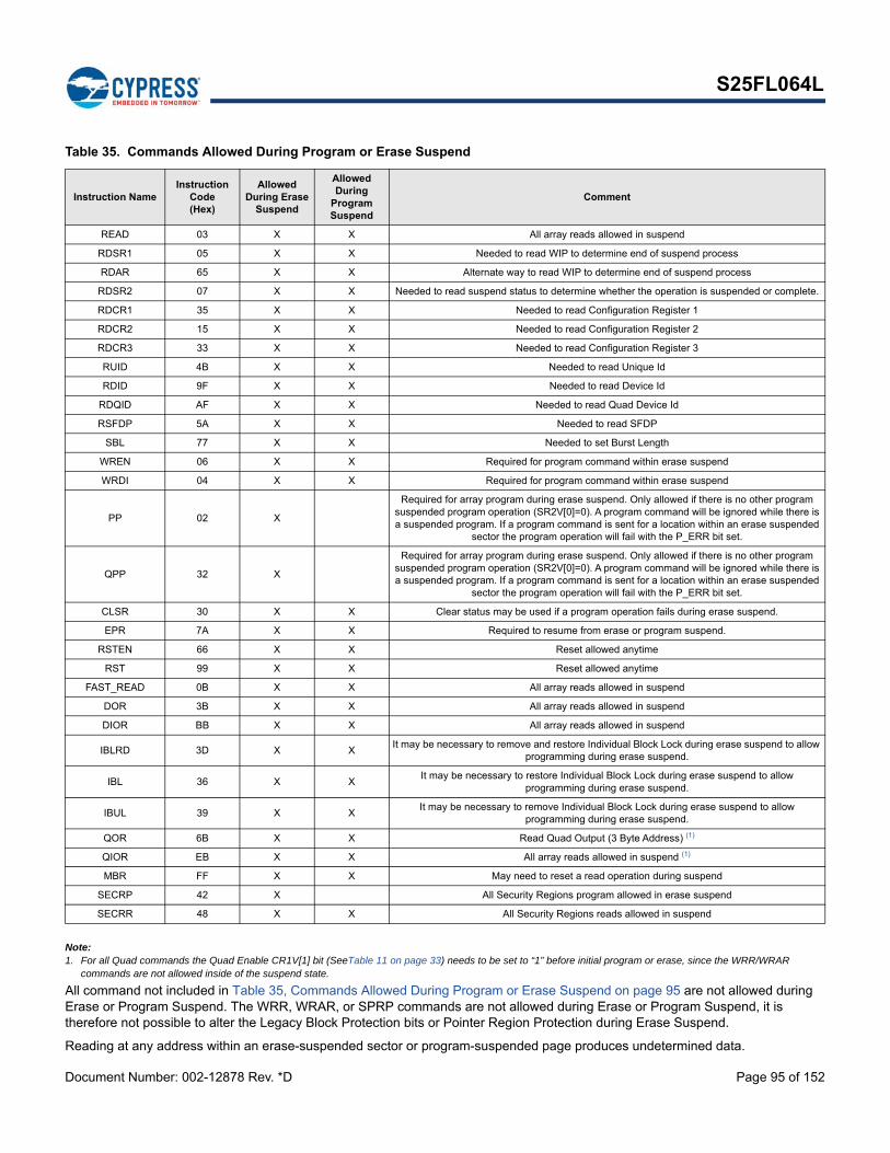
Document Number: 002-12878 Rev. *D Page 95 of 152
S25FL064L
Table 35. Commands Allowed During Program or Erase Suspend
Note:1. For all Quad commands the Quad Enable CR1V[1] bit (SeeTable 11 on page 33) needs to be set to “1” before initial program or erase, since the WRR/WRAR
commands are not allowed inside of the suspend state.
All command not included in Table 35, Commands Allowed During Program or Erase Suspend on page 95 are not allowed during Erase or Program Suspend. The WRR, WRAR, or SPRP commands are not allowed during Erase or Program Suspend, it is therefore not possible to alter the Legacy Block Protection bits or Pointer Region Protection during Erase Suspend.
Reading at any address within an erase-suspended sector or program-suspended page produces undetermined data.
Instruction NameInstruction
Code (Hex)
Allowed During Erase
Suspend
Allowed During
Program Suspend
Comment
READ 03 X X All array reads allowed in suspend
RDSR1 05 X X Needed to read WIP to determine end of suspend process
RDAR 65 X X Alternate way to read WIP to determine end of suspend process
RDSR2 07 X X Needed to read suspend status to determine whether the operation is suspended or complete.
RDCR1 35 X X Needed to read Configuration Register 1
RDCR2 15 X X Needed to read Configuration Register 2
RDCR3 33 X X Needed to read Configuration Register 3
RUID 4B X X Needed to read Unique Id
RDID 9F X X Needed to read Device Id
RDQID AF X X Needed to read Quad Device Id
RSFDP 5A X X Needed to read SFDP
SBL 77 X X Needed to set Burst Length
WREN 06 X X Required for program command within erase suspend
WRDI 04 X X Required for program command within erase suspend
PP 02 X
Required for array program during erase suspend. Only allowed if there is no other program suspended program operation (SR2V[0]=0). A program command will be ignored while there is a suspended program. If a program command is sent for a location within an erase suspended
sector the program operation will fail with the P_ERR bit set.
QPP 32 X
Required for array program during erase suspend. Only allowed if there is no other program suspended program operation (SR2V[0]=0). A program command will be ignored while there is a suspended program. If a program command is sent for a location within an erase suspended
sector the program operation will fail with the P_ERR bit set.
CLSR 30 X X Clear status may be used if a program operation fails during erase suspend.
EPR 7A X X Required to resume from erase or program suspend.
RSTEN 66 X X Reset allowed anytime
RST 99 X X Reset allowed anytime
FAST_READ 0B X X All array reads allowed in suspend
DOR 3B X X All array reads allowed in suspend
DIOR BB X X All array reads allowed in suspend
IBLRD 3D X XIt may be necessary to remove and restore Individual Block Lock during erase suspend to allow
programming during erase suspend.
IBL 36 X XIt may be necessary to restore Individual Block Lock during erase suspend to allow
programming during erase suspend.
IBUL 39 X XIt may be necessary to remove Individual Block Lock during erase suspend to allow
programming during erase suspend.
QOR 6B X X Read Quad Output (3 Byte Address) (1)
QIOR EB X X All array reads allowed in suspend (1)
MBR FF X X May need to reset a read operation during suspend
SECRP 42 X All Security Regions program allowed in erase suspend
SECRR 48 X X All Security Regions reads allowed in suspend

Document Number: 002-12878 Rev. *D Page 96 of 152
S25FL064L
After an erase-suspended program operation is complete, the device returns to the erase-suspend mode. The system can determine the status of the program operation by reading the WIP bit in the Status Register, just as in the standard program operation.
Figure 88. Program or Erase Suspend Command Sequence
This command is also supported in QPI mode. In QPI mode the instruction is shifted in on IO0-IO3.
Figure 89. Program or Erase Suspend Command Sequence QPI mode
Figure 90. Program or Erase Suspend Command with Continuing Instruction Commands Sequence
8.6.6 Erase or Program Resume (EPR 7Ah)After program or read operations are completed during a program or erase suspend the Erase or Program Resume command is sent to continue the suspended operation.
After an Erase or Program Resume command is issued, the WIP bit in the Status Register 1 will be set to a 1 and the suspended operation will resume if one is suspended. If there is no suspended program or erase operation the resume command is ignored.
Program or erase operations may be interrupted as often as necessary e.g. a program suspend command could immediately follow a program resume command but, but in order for a program or erase operation to progress to completion there must be some periods of time between resume and the next suspend command greater than or equal to tRNS. See Table 56, Program or Erase Suspend AC Parameters on page 139.
The Program Suspend Status bit in the Status Register 1 (SR2[0]) can be used to determine if a programming operation has been suspended or was completed at the time WIP changes to 0. The Erase Suspend Status bit in the Status Register 1 (SR2[1]) can be used to determine if an erase operation has been suspended or was completed at the time WIP changes to 0. See Section 6.6.2, Status Register 2 Volatile (SR2V) on page 31.
CS#
SCK
SI_IO0
SO_IO1
Phase
7 6 5 4 3 2 1 0
Instruction
CS#
SCLK
IO0
IO1
IO2
IO3
Phase
4 0
5 1
6 2
7 3
Instruction
CS#
SCK
SI_IO0
SO
Phase
Phase
7 6 5 4 3 2 1 0 7 6 5 4 3 2 1 0 7 6 5 4 3 2 1 0
7 6 5 4 3 2 1 0
Suspend Instruction Read Status Instruction Status Instr. During Suspend
Repeat Status Read Until Suspended
tSL

Document Number: 002-12878 Rev. *D Page 97 of 152
S25FL064L
An Erase or Program Resume command must be written to resume a suspended operation.
Figure 91. Erase or Program Resume command Sequence
This command is also supported in QPI mode. In QPI mode the instruction is shifted in on IO0-IO3.
Figure 92. Erase or Program Resume command Sequence QPI mode
8.7 Security Regions Array CommandsThe Security Regions commands select which region to use by address A15 to A8 as shown below.
Security Region 0: A23-16 = 00h; A15-8 = 00h; A7-0 = byte address
Security Region 1: A23-16 = 00h; A15-8 = 01h; A7-0 = byte address
Security Region 2: A23-16 = 00h; A15-8 = 02h; A7-0 = byte address
Security Region 3: A23-16 = 00h; A15-8 = 03h; A7-0 = byte address
8.7.1 Security Region Erase (SECRE 44h)The Security Region Erase command erases data in the Security Region, which is in a different address space from the main array data. The Security Region is 1024 bytes so, the address bits forS25FL064L (A22 to A10) must be zero for this command. Each region can be individually erased. Refer to Section 6.5, Security Regions Address Space on page 28 for details on the Security Region.
Before the Security Region Erase command can be accepted by the device, a Write Enable (WREN) command must be issued and decoded by the device, which sets the Write Enable Latch (WEL) in the Status Register to enable any write operations. The WIP bit in SR1V may be checked to determine when the operation is completed. The E_ERR bit in SR2V may be checked to determine if any error occurred during the operation.
The Security Region Lock Bits (CR1NV[2-5]) in the Configuration Register 1 can be used to protect the Security Regions for erase. Once a lock bit is set to 1, the corresponding Security Region will be permanently locked, Attempting to erase a region that is locked will fail with the E_ERR bit in SR2V[6] set to “1”.
When the Protection Register NVLOCK Bit = “0”, Security Regions 2 and 3 are protected from program or erase. Attempting to erase in a region that locked will fail with the E_ERR bits in SR2V[6] set to “1”. See Section 7.7.2.1, NVLOCK Bit (PR[0]) on page 56.
The Password Protection Mode Lock Bit (IRP[2]) allows regions 2 and 3 to be protected from erase operations until the correct password is provided to enable erasing of these Security Regions. Attempting to erase in a region that is password locked will fail with the E_ERR bit in SR2V[6] set to “1”. Security Region Read Password Protection on page 57
The protocol of the Security Region Erase command is the same as the Sector Erase command. See Section 8.6.1, Sector Erase (SE 20h or 4SE 21h) on page 91 for the command sequence. QPI Mode is supported.
CS#
SCK
SI_IO0
SO_IO1
Phase
7 6 5 4 3 2 1 0
Instruction
CS#
SCLK
IO0
IO1
IO2
IO3
Phase
4 0
5 1
6 2
7 3
Instruction

Document Number: 002-12878 Rev. *D Page 98 of 152
S25FL064L
8.7.2 Security Region Program (SECRP 42h)The Security Region Program command programs data in the Security Region, which is in a different address space from the main array data. The Security Region is 1024 bytes so, the address bits forS25FL064L (A22 to A10) must be zero for this command. Refer to Section 6.5, Security Regions Address Space on page 28 for details on the Security Region.
Before the Security Region Program command can be accepted by the device, a Write Enable (WREN) command must be issued and decoded by the device, which sets the Write Enable Latch (WEL) in the Status Register to enable any write operations. The WIP bit in SR1V may be checked to determine when the operation is completed. The P_ERR bit in SR2V may be checked to determine if any error occurred during the operation.
To program the Security Region array in bit granularity, the rest of the bits within a data byte can be set to “1”.
Each region in the Security Region memory space can be programmed one or more times, provided that the region is not locked. However, for the best data integrity, it is recommended that one or more 16 byte length and aligned groups of bytes be programed together and programmed only once between erase operations within each region.
The Security Region Lock Bits (CR1NV[2-5]) in the Configuration Register 1 can be used to protect the Security Regions for Programming. Once a lock bit is set to 1, the corresponding Security Region will be permanently locked. Attempting to program zeros or ones in a region that is locked (protected) will fail with the P_ERR bit in SR2V[5] set to “1”. Programming ones in a un-protected area does not cause an error and does not set P_ERR. (see Configuration Register 1 on page 32 for detail descriptions).
When the Protection Register NVLOCK Bit = “0”, Security Regions 2 and 3 are protected from program or erase. Attempting to program in a region that locked will fail with the P_ERR bit in SR2V[5] set to “1”. See Section 7.7.2.1, NVLOCK Bit (PR[0]) on page 56.
The Password Protection Mode Lock Bit (IRP[2]) allows regions 2 and 3 to be protected from programming operations until the correct password is provided to enable programming of these Security Regions 2 and 3. Attempting to program in a region that is password locked will fail with the P_ERR bit in SR2V[5] set to “1”. See Password Protection Mode on page 56.
The protocol of the Security Region Program command is the same as the Page Program command. See Section 8.5.1.1, Page Programming on page 89 for the command sequence. QPI Mode is supported.
8.7.3 Security Regions Read (SECRR 48h)The Security Region Read (SECRR) command provides a way to read data from the Security Regions. The Security Region is 1024 bytes so, the address bits forS25FL064L (A22 to A10) must be zero for this command. Refer to Section 6.5, Security Regions Address Space on page 28 for details on the Security Regions.
The instruction is followed by a 3 or 4 Byte address (depending on the address length configuration CR2V[0], followed by a number of latency (dummy) cycles set by CR3V[3:0]. Then the selected register data are returned. The protocol of the Security Region Read command will not wrap to the starting address after the Security Region address is at its maximum; instead, the data beyond the maximum address will be undefined. The Security Region Read command read latency is set by the latency value in CR3V[3:0].
The Security Region Read Password Mode Enable Bit (IRP[6]) allows regions 3 to be protected from read operations until the correct password is provided to enable reading of this Security Region. Attempting to read in region 3 that is password locked will return invalid and undefined data. See Security Region Read Password Protection on page 57
Figure 93. Security Regions Read Command Sequence
Note:1. A = MSB of address = 23 for Address length CR2V[0] = 0, or 31 for CR2V[0]=1.
CS#
SCK
SI_IO0
SO_IO1
Phase
7 6 5 4 3 2 1 0 A 1 0
7 6 5 4 3 2 1 0
Instruction Address Dummy Cycles Data 1

Document Number: 002-12878 Rev. *D Page 99 of 152
S25FL064L
This command is also supported in QPI mode. In QPI mode the instruction and address is shifted in and returning data out on IO0-IO3.
Figure 94. Security Regions Read Command Sequence QPI mode
Note:1. A = MSB of address = 23 for CR2V[0]=0, or 31 for CR2V[0]=1.
8.8 Individual Block Lock CommandsIn order to use Individual Block Lock, the IBL protection scheme must be selected by the WPS bit in Configuration Register 2 CR2V[2]=1. If if IBL protection scheme is not selected CR2V[2]=0 the IBL commands are ignored.
Individual Block Lock Bits (IBL) are volatile, with one for each sector / block, and can be individually modified. By issuing the IBL or GBL commands, a IBL bit is set to “0” protecting each related sector / block. By issuing the IBUL or GUL commands, a IBL bit is cleared to “1” unprotecting each related sector or block. By issuing the IBLRD command the state of each IBL bit protection can be read.
8.8.1 IBL Read (IBLRD 3Dh or 4IBLRD E0h)The IBLRD/4IBLRD command allows reading the state of each IBL bit protection.
The instruction is latched into SI by the rising edge of the SCK signal. The instruction is followed by the 24 or 32-Bit address, depending on the address length configuration CR2V[0], selecting location zero within the desired sector.
Then the 8-bit IBL access register contents are shifted out on the serial output SO/IO1. Each bit is shifted out at the SCK frequency by the falling edge of the SCK signal. It is possible to read the same IBL access register continuously by providing multiples of eight clock cycles. The address of the IBL register does not increment so this is not a means to read the entire IBL array. Each location must be read with a separate IBL Read command.
Figure 95. IBLRD Command Sequence
Notes:1. A = MSB of address = 23 for Address length (CR2V[0] = 0, or 31 for CR2V[0]=1 with command 3Dh.
2. A = MSB of address = 31 with command E0h.
This command is also supported in QPI mode. In QPI mode the instruction and address is shifted in and returning data out on IO0-IO3.
CS#
SCLK
IO0
IO1
IO2
IO3
Phase
4 0 A-3 4 0 4 0 4 0 4 0 4 0
5 1 A-2 5 1 5 1 5 1 5 1 5 1
6 2 A-1 6 2 6 2 6 2 6 2 6 2
7 3 A 7 3 7 3 7 3 7 3 7 3
Instruct. Address Dummy D1 D2 D3 D4
CS#
SCK
SI_IO0
SO_IO1
Phase
7 6 5 4 3 2 1 0 A 1 0
7 6 5 4 3 2 1 0
Instruction Address Dummy Cycles Output IBL

Document Number: 002-12878 Rev. *D Page 100 of 152
S25FL064L
Figure 96. IBLRD Command Sequence QPI
Notes:1. A = MSB of address = 23 for Address length (CR2V[0] = 0, or 31 for CR2V[0]=1 with command 3Dh.
2. A = MSB of address = 31 with command E0h.
8.8.2 IBL Lock (IBL 36h or 4IBL E1h)The IBL/4IBL commands sets the selected IBL bit to “0” protecting each related sector / block.
The IBL command is entered by driving CS# to the logic low state, followed by the instruction, followed by the 24 or 32-Bit address, depending on the address length configuration CR2V[0]. The IBL command affects the WIP bits of the Status and Configuration Registers in the same manner as any other programming operation.
CS# must be driven to the logic high state after the 24 or 32-Bit address (depending on the address length configuration CR2V[0]) has been latched in. As soon as CS# is driven to the logic high state, the self-timed IBL operation is initiated. While the IBL operation is in progress, the Status Register may be read to check the value of the Write-In Progress (WIP) bit. The Write-In Progress (WIP) bit is a “1” during the self-timed IBL operation, and is a “0” when it is completed.
Figure 97. IBL Command Sequence
Notes:1. A = MSB of address = 23 for Address length (CR2V[0] = 0, or 31 for CR2V[0]=1 with command 36h.
2. A = MSB of address = 31 with command E1h
This command is also supported in QPI mode. In QPI mode the instruction and address is shifted in on IO0-IO3.
Figure 98. IBL Command Sequence QPI Mode
Notes:1. A = MSB of address = 23 for Address length (CR2V[0] = 0, or 31 for CR2V[0]=1 with command 36h.
2. A = MSB of address = 31 with command E1h.
CS#
SCLK
IO0
IO1
IO2
IO3
Phase
4 0 A-3 4 0 4 0 4 0
5 1 A-2 5 1 5 1 5 1
6 2 A-1 6 2 6 2 6 2
7 3 A 7 3 7 3 7 3
Instruct. Address Dummy IBL Repeat IBL
CS#
SCK
SI_IO0
SO_IO1
Phase
7 6 5 4 3 2 1 0 A 1 0
Instruction Address
CS#
SCLK
IO0
IO1
IO2
IO3
Phase
4 0 A-3 4 0
5 1 A-2 5 1
6 2 A-1 6 2
7 3 A 7 3
Instructtion Address

Document Number: 002-12878 Rev. *D Page 101 of 152
S25FL064L
8.8.3 IBL Unlock (IBUL 39h or 4IBUL E2h)The IBUL/4IBULcommands clears the selected IBL bit to “1” unprotecting each related sector / block.
The IBUL command is entered by driving CS# to the logic low state, followed by the instruction, followed by the 24 or 32-Bit address, depending on the address length configuration CR2V[0]. The IBUL command affects the WIP bits of the Status and Configuration Registers in the same manner as any other programming operation.
CS# must be driven to the logic high state after the 24 or 32-Bit address (depending on the address length configuration CR2V[0]) has been latched in. As soon as CS# is driven to the logic high state, the self-timed IBL operation is initiated. While the IBUL operation is in progress, the Status Register may be read to check the value of the Write-In Progress (WIP) bit. The Write-In Progress (WIP) bit is a “1” during the self-timed IBUL operation, and is a “0” when it is completed.
Figure 99. IBUL Command Sequence
Notes:1. A = MSB of address = 23 for Address length (CR2V[0] = 0, or 31 for CR2V[0]=1 with command 39h.
2. A = MSB of address = 31 with command E2h.
This command is also supported in QPI mode. In QPI mode the instruction and address is shifted in on IO0-IO3.
Figure 100. IBUL Command Sequence QPI Mode
Notes:1. A = MSB of address = 23 for Address length (CR2V[0] = 0, or 31 for CR2V[0]=1 with command 39h.
2. A = MSB of address = 31 with command E2h.
8.8.4 Global IBL Lock (GBL 7Eh)The GBL commands sets all the IBL bits to “0” protecting all sectors / blocks.
CS# must be driven into the logic high state after the eighth bit of the instruction byte has been latched in on SI. This will initiate the GBL. If CS# is not driven high after the last bit of instruction, the GBL operation will not be executed.
As soon as CS# is driven into the logic high state, the GBL will be initiated. With the GBL in progress, the user can read the value of the Write-In Progress (WIP) bit to determine when the operation has been completed. The WIP bit will indicate a “1” when the GBL is in progress and a “0” when the GBL has been completed.
CS#
SCK
SI_IO0
SO_IO1
Phase
7 6 5 4 3 2 1 0 A 1 0
Instruction Address
CS#
SCLK
IO0
IO1
IO2
IO3
Phase
4 0 A-3 4 0
5 1 A-2 5 1
6 2 A-1 6 2
7 3 A 7 3
Instructtion Address

Document Number: 002-12878 Rev. *D Page 102 of 152
S25FL064L
Figure 101. Global IBL Lock (GBL) Command Sequence
This command is also supported in QPI mode. In QPI mode the instruction is shifted in on IO0-IO3.
Figure 102. Global IBL Lock (GBL) Command Sequence QPI mode
8.8.5 Global IBL Unlock (GBUL 98h)The GBUL commands clears all the IBL bits to “1” unprotecting all sectors / blocks.
CS# must be driven into the logic high state after the eighth bit of the instruction byte has been latched in on SI. This will initiate the GBUL If CS# is not driven high after the last bit of instruction, the GBUL operation will not be executed.
As soon as CS# is driven into the logic high state, the GBL will be initiated. With the GBL in progress, the user can read the value of the Write-In Progress (WIP) bit to determine when the operation has been completed. The WIP bit will indicate a “1” when the GBUL is in progress and a “0” when the GBUL has been completed.
Figure 103. Global IBL Unlock (GBUL) Command Sequence
This command is also supported in QPI mode. In QPI mode the instruction is shifted in on IO0-IO3.
Figure 104. Global IBL Unlock (GBUL) Command Sequence QPI mode
CS#
SCK
SI_IO0
SO_IO1
Phase
7 6 5 4 3 2 1 0
Instruction
CS#
SCLK
IO0
IO1
IO2
IO3
Phase
4 0
5 1
6 2
7 3
Instruction
CS#
SCK
SI_IO0
SO_IO1
Phase
7 6 5 4 3 2 1 0
Instruction
CS#
SCLK
IO0
IO1
IO2
IO3
Phase
4 0
5 1
6 2
7 3
Instruction

Document Number: 002-12878 Rev. *D Page 103 of 152
S25FL064L
8.9 Pointer Region Command
8.9.1 Set Pointer Region Protection (SPRP FBh or 4SPRP E3h)
The SPRP or 4SPRP command is ignored during a suspend operation because the pointer value cannot be erased and re-programmed during a suspend.
The SPRP or 4SPRP command is ignored if default Power Supply Lock-down protection NVLOCK PR[0]=0 or Power Supply Lock-down protection enabled IRP[1]=0 or Password Protection enabled IRP[2]=0 and NVLOCK PR[0]=0.
Before the SPRP or 4SPRP command can be accepted by the device, a Write Enable (WREN) command must be issued. After the Write Enable (WREN) command has been decoded, the device will set the Write Enable Latch (WEL) in the Status Register to enable any write operations.
The SPRP or 4SPRP command is entered by driving CS# to the logic low state, followed by the instruction, followed by the 24 or 32-Bit address, depending on the address length configuration CR2V[0], see Pointer Region Protection (PRP) on page 52 for details on address values to select protection options.
CS# must be driven to the logic high state after the last bit of address has been latched in. If not, the SPRP command is not executed. As soon as CS# is driven to the logic high state, the self-timed SPRP operation is initiated. While the SPRP operation is in progress, the Status Register may be read to check the value of the Write-In Progress (WIP) bit. The Write-In Progress (WIP) bit is a “1” during the self-timed SPRP operation, and is a “0” when it is completed. When the SPRP operation is completed, the Write Enable Latch (WEL) is set to a “0”. The SPRP or 4SPRP command will set the P_ERR or E_ERR bits if there is a failure in the Set Pointer Region Protection operation.
For details on the address pointer defining a sector boundary between protected and unprotected regions in the memory, see Pointer Region Protection (PRP) on page 52.
Figure 105. SPRP Command Sequence
Notes:1. A = MSB of address = 23 for Address length (CR2V[0] = 0, or 31 for CR2V[0]=1 with command FDh.
2. A = MSB of address = 31 with command E3h.
This command is also supported in QPI mode. In QPI mode the instruction and address is shifted in on IO0-IO3.
Figure 106. SPRP Command Sequence QPI Mode
Notes:1. A = MSB of address = 23 for Address length (CR2V[0] = 0, or 31 for CR2V[0]=1 with command FDh.
2. A = MSB of address = 31 with command E3h.
CS#
SCK
SI_IO0
SO_IO1
Phase
7 6 5 4 3 2 1 0 A 1 0
Instruction Address
CS#
SCLK
IO0
IO1
IO2
IO3
Phase
4 0 A-3 4 0
5 1 A-2 5 1
6 2 A-1 6 2
7 3 A 7 3
Instructtion Address

Document Number: 002-12878 Rev. *D Page 104 of 152
S25FL064L
8.10 Individual and Region Protection (IRP) Commands
8.10.1 IRP Register Read (IRPRD 2Bh)The IRP Register Read instruction 2Bh is shifted into SI/IO0 by the rising edge of the SCK signal followed by one dummy cycle. This latency period allows the device’s internal circuitry enough time to access data at the initial address. During latency cycles, the data value on IO0-IO3 are “don’t care” and may be high impedance.
Then the 16-bit IRP register contents are shifted out on the serial output S0/IO1, least significant byte first. Each bit is shifted out at the SCK frequency by the falling edge of the SCK signal. It is possible to read the IRP register continuously by providing multiples of 16 clock cycles.
Figure 107. IRPRD Command Sequence
This command is also supported in QPI mode. In QPI mode the instruction is shifted in and returning data out on IO0-IO3.
Figure 108. IRPRD Command Sequence – QPI Mode
8.10.2 IRP Program (IRPP 2Fh)Before the IRP Program (IRPP) command can be accepted by the device, a Write Enable (WREN) command must be issued. After the Write Enable (WREN) command has been decoded, the device will set the Write Enable Latch (WEL) in the Status Register to enable any write operations.
The IRPP command is entered by driving CS# to the logic low state, followed by the instruction and two data bytes on SI, least significant byte first. The IRP Register is two data bytes in length.
The IRPP command affects the P_ERR and WIP bits of the Status and Configuration Registers in the same manner as any other programming operation.
CS# input must be driven to the logic high state after the sixteenth bit of data has been latched in. If not, the IRPP command is not executed. As soon as CS# is driven to the logic high state, the self-timed IRPP operation is initiated. While the IRPP operation is in progress, the Status Register may be read to check the value of the Write-In Progress (WIP) bit. The Write-In Progress (WIP) bit is a “1” during the self-timed IRPP operation, and is a “0” when it is completed. When the IRPP operation is completed, the Write Enable Latch (WEL) is set to a “0”.
CS#
SCK
SI_IO0
SO_IO1
Phase
7 6 5 4 3 2 1 0
7 6 5 4 3 2 1 0 7 6 5 4 3 2 1 0
Instruction DY Output IRP Low Byte Output IRP High Byte
CS#
SCLK
IO0
IO1
IO2
IO3
Phase
4 0 4 0 4 0
5 1 5 1 5 1
6 2 6 2 6 2
7 3 7 3 7 3
Instruct. Dummy IRP Low Byte IRP High Byte

Document Number: 002-12878 Rev. *D Page 105 of 152
S25FL064L
Figure 109. IRP Program (IRPP) Command
This command is also supported in QPI mode. In QPI mode the instruction and data is shifted in on IO0-IO3.
Figure 110. IRP Program (IRPP) Command QPI
8.10.3 Protection Register Read (PRRD A7h)The Protection Register Read (PRRD) command allows the Protection Register contents to be read out of SO/IO1. The Read instruction A7h is shifted into SI by the rising edge of the SCK signal followed by one dummy cycle. This latency period allows the device’s internal circuitry enough time to access data at the initial address. During latency cycles, the data value on IO0-IO3 are “don’t care” and may be high impedance.
Then the 8-bit Protection Register contents are shifted out on the serial output SO/IO1. Each bit is shifted out at the SCK frequency by the falling edge of the SCK signal. It is possible to read the Protection register continuously by providing multiples of eight clock cycles.
The Protection Register contents may only be read when the device is in standby state with no other operation in progress.
Figure 111. Protection Register Read (PRRD) Command Sequence
This command is also supported in QPI mode. In QPI mode the instruction is shifted in and returning data out on IO0-IO3.
CS#
SCK
SI_IO0
SO_IO1
Phase
7 6 5 4 3 2 1 0 7 6 5 4 3 2 1 0 7 6 5 4 3 2 1 0
Instruction Input IRP Low Byte Input IRP High Byte
CS#
SCLK
IO0
IO1
IO2
IO3
Phase
4 0 4 0 C 8
5 1 5 1 D 9
6 2 6 2 E A
7 3 7 3 F B
Instruct. IRP Low Byte IRP High Byte
CS#
SCK
SI_IO0
SO_IO1
Phase
7 6 5 4 3 2 1 0
7 6 5 4 3 2 1 0 7 6 5 4 3 2 1 0
Instruction DY Register Read Repeat Register Read

Document Number: 002-12878 Rev. *D Page 106 of 152
S25FL064L
Figure 112. Protection Register Read (PRRD) Command Sequence – QPI Mode
8.10.4 Protection Register Lock (PRL A6h)The Protection Register Lock (PRL) command clears the NVLOCK bit (PR[0]) to zero and loads the IRP[6] value in to SECRRP (PR[6]). See Section 6.6.8, Protection Register (PR) on page 42. Before the PRL command can be accepted by the device, a Write Enable (WREN) command must be issued and decoded by the device, which sets the Write Enable Latch (WEL) in the Status Register to enable any write operations.
The PRL command is entered by driving CS# to the logic low state, followed by the instruction.
CS# must be driven to the logic high state after the eighth bit of instruction has been latched in. If not, the PRL command is not executed. As soon as CS# is driven to the logic high state, the self-timed PRL operation is initiated. While the PRL operation is in progress, the Status Register may still be read to check the value of the Write-In Progress (WIP) bit. The Write-In Progress (WIP) bit is a “1” during the self-timed PRL operation, and is a “0” when it is completed. When the PRL operation is completed, the Write Enable Latch (WEL) is set to a “0”.
Figure 113. Protection Register Lock (PRL) Command Sequence
This command is also supported in QPI mode. In QPI mode the instruction is shifted in on IO0-IO3.
Figure 114. Protection Register Lock (PRL) Command Sequence – QPI Mode
CS#
SCLK
IO0
IO1
IO2
IO3
Phase
4 0 4 0 4 0
5 1 5 1 5 1
6 2 6 2 6 2
7 3 7 3 7 3
Instruct. Dummy Register Read Register Read
CS#
SCK
SI_IO0
SO_IO1
Phase
7 6 5 4 3 2 1 0
Instruction
CS#
SCLK
IO0
IO1
IO2
IO3
Phase
4 0
5 1
6 2
7 3
Instruction

Document Number: 002-12878 Rev. *D Page 107 of 152
S25FL064L
8.10.5 Password Read (PASSRD E7h)The correct password value may be read only after it is programmed and before the Password Mode has been selected by programming the Password Protection Mode bit to 0 in the IRP Register (IRP[2]). After the Password Protection Mode is selected the password is no longer readable, the PASSRD command will output undefined data.
The PASSRD command is shifted into SI followed by one dummy cycle. This latency period allows the device’s internal circuitry enough time to access data at the initial address. During latency cycles, the data value on are “don’t care” and may be high impedance.
Then the 64-bit Password is shifted out on the serial output, least significant byte first, most significant bit of each byte first. Each bit is shifted out at the SCK frequency by the falling edge of the SCK signal. It is possible to read the Password continuously by providing multiples of 64 clock cycles.
Figure 115. Password Read (PASSRD) Command Sequence
This command is also supported in QPI mode. In QPI mode the instruction is shifted in and returning data out on IO0-IO3.
Figure 116. Password Read (PASSRD) Command Sequence – QPI Mode
8.10.6 Password Program (PASSP E8h)Before the Password Program (PASSP) command can be accepted by the device, a Write Enable (WREN) command must be issued and decoded by the device. After the Write Enable (WREN) command has been decoded, the device sets the Write Enable Latch (WEL) to enable the PASSP operation.
The password can only be programmed before the Password Mode is selected by programming the Password Protection Mode bit to 0 in the IRP Register (IRP[2]). After the Password Protection Mode is selected the PASSP command is ignored.
The PASSP command is entered by driving CS# to the logic low state, followed by the instruction and the password data bytes on SI/IO0, least significant byte first, most significant bit of each byte first. The password is sixty-four (64) bits in length.
CS# must be driven to the logic high state after the sixty-fourth (64th) bit of data has been latched. If not, the PASSP command is not executed. As soon as CS# is driven to the logic high state, the self-timed PASSP operation is initiated. While the PASSP operation is in progress, the Status Register may be read to check the value of the Write-In Progress (WIP) bit. The Write-In Progress (WIP) bit is a “1” during the self-timed PASSP cycle, and is a “0” when it is completed. The PASSP command can report a program error in the P_ERR bit of the status register. When the PASSP operation is completed, the Write Enable Latch (WEL) is set to a “0”.
CS#
SCK
SI_IO0
SO_IO1
IO2-IO3
Phase
7 6 5 4 3 2 1 0
7 6 5 4 3 2 1 0 7 6 5 4 3 2 1 0
Instruction DY Data 1 Data 8
CS#
SCLK
IO0
IO1
IO2
IO3
Phase
4 0 4 0 4 0 4 0
5 1 5 1 5 1 5 1
6 2 6 2 6 2 6 2
7 3 7 3 7 3 7 3
Instruct. Dummy Data 1 Data 8

Document Number: 002-12878 Rev. *D Page 108 of 152
S25FL064L
Figure 117. Password Program (PASSP) Command Sequence
This command is also supported in QPI mode. In QPI mode the instruction and data is shifted in on IO0-IO3.
Figure 118. Password Program (PASSP) Command Sequence QPI mode
8.10.7 Password Unlock (PASSU EAh)The PASSU command is entered by driving CS# to the logic low state, followed by the instruction and the password data bytes on SI, least significant byte first, most significant bit of each byte first. The password is sixty-four (64) bits in length.
CS# must be driven to the logic high state after the sixty-fourth (64th) bit of data has been latched. If not, the PASSU command is not executed. As soon as CS# is driven to the logic high state, the self-timed PASSU operation is initiated. While the PASSU operation is in progress, the Status Register may be read to check the value of the Write-In Progress (WIP) bit. The Write-In Progress (WIP) bit is a “1” during the self-timed PASSU cycle, and is a “0” when it is completed.
If the PASSU command supplied password does not match the hidden password in the Password Register, an error is reported by setting the P_ERR bit to 1. The WIP bit of the status register also remains set to 1. It is necessary to use the CLSR command to clear the status register, the software reset command (RSTEN 66h followed by RST 99h) to reset the device, or drive the RESET# and IO3 / RESET# input to initiate a hardware reset, in order to return the P_ERR and WIP bits to 0. This returns the device to standby state, ready for new commands such as a retry of the PASSU command.
If the password does match, the NVLOCK bit is set to “1”.
Figure 119. Password Unlock (PASSU) Command Sequence
This command is also supported in QPI mode. In QPI mode the instruction and data is shifted in on IO0-IO3.
CS#
SCK
SI_IO0
SO_IO1
Phase
7 6 5 4 3 2 1 0 7 6 5 4 3 2 1 0 7 6 5 4 3 2 1 0
Instruction Password Byte 1 Password Byte 8
CS#
SCLK
IO0
IO1
IO2
IO3
Phase
4 0 4 0 4 0 4 0
5 1 5 1 5 1 5 1
6 2 6 2 6 2 6 2
7 3 7 3 7 3 7 3
Instruct. Password Byte 1 Password Byte 8
CS#
SCK
SI_IO0
SO_IO1
Phase
7 6 5 4 3 2 1 0 7 6 5 4 3 2 1 0 7 6 5 4 3 2 1 0
Instruction Password Byte 1 Password Byte 8

Document Number: 002-12878 Rev. *D Page 109 of 152
S25FL064L
Figure 120. Password Unlock (PASSU) Command Sequence QPI mode
8.11 Reset CommandsSoftware controlled Reset commands restore the device to its initial power up state, by reloading volatile registers from non-volatile default values. If a software reset is initiated during a Erase, Program or writing of a Register operation the data in that Sector, Page or Register is not stable, the operation that was interrupted needs to be initiated again.
However, the volatile SRP1 bit in the Configuration register CR1V[0] and the volatile NVLOCK bit in the Protection Register are not changed by a software reset. The software reset cannot be used to circumvent the SRP1 or NVLOCK bit protection mechanisms for the other security configuration bits.
The SRP1 bit and the NVLOCK bit will remain set at their last value prior to the software reset. To clear the SRP1 bit and set the NVLOCK bit to its protection mode selected power on state, a full power-on-reset sequence or hardware reset must be done.
A software reset command (RSTEN 66h followed by RST 99h) is executed when CS# is brought high at the end of the instruction and requires tRPH time to execute.
In the case of a previous Power-up Reset (POR) failure to complete, a reset command triggers a full power up sequence requiring tPU to complete.
Figure 121. Software / Mode Bit Reset Command Sequence
This command is also supported in QPI mode. In QPI mode the instruction is shifted in on IO0-IO3.
Figure 122. Software Reset / Mode Bit Command Sequence – QPI Mode
CS#
SCLK
IO0
IO1
IO2
IO3
Phase
4 0 4 0 4 0 4 0
5 1 5 1 5 1 5 1
6 2 6 2 6 2 6 2
7 3 7 3 7 3 7 3
Instruct. Password Byte 1 Password Byte 8
CS#
SCK
SI_IO0
SO_IO1
Phase
7 6 5 4 3 2 1 0
Instruction
CS#
SCLK
IO0
IO1
IO2
IO3
Phase
4 0
5 1
6 2
7 3
Instruction

Document Number: 002-12878 Rev. *D Page 110 of 152
S25FL064L
8.11.1 Software Reset Enable (RSTEN 66h)The Reset Enable (RSTEN) command is required immediately before a software reset command (RST 99h) such that a software reset is a sequence of the two commands. Any command other than RST following the RSTEN command, will clear the reset enable condition and prevent a later RST command from being recognized.
8.11.2 Software Reset (RST 99h)The Reset (RST) command immediately following a RSTEN command, initiates the software reset process. Any command other than RST following the RSTEN command, will clear the reset enable condition and prevent a later RST command from being recognized.
8.11.3 Mode Bit Reset (MBR FFh)The Mode Bit Reset (MBR) command is used to return the device from continuous high performance read mode back to normal standby awaiting any new command. Because the hardware RESET# input may be disabled and a device that is in a continuous high performance read mode may not recognize any normal SPI command, a system hardware reset or software reset command may not be recognized by the device. It is recommended to use the MBR command after a system reset when the RESET# signal is not available or, before sending a software reset, to ensure the device is released from continuous high performance read mode.
The MBR command sends Ones on SI/IO0for eight SCK cycles. IO1-IO3 are “don’t care” during these cycles.
8.12 Deep Power Down Commands
8.12.1 Deep Power-Down (DPD B9h)Although the standby current during normal operation is relatively low, standby current can be further reduced with the Deep Power-Down command. The lower power consumption makes the Deep Power-down (DPD) command especially useful for battery powered applications (see ICC1 and ICC2 in (Section 11.6, DC Characteristics on page 127). The command is initiated by driving the CS# pin low and shifting the instruction code “B9h”.
The CS# pin must be driven high after the eighth bit has been latched. If this is not done the Deep Power-Down command will not be executed. After CS# is driven high, the power-down state will be entered within the time duration of tDP (Table 53 on page 134). While in the power-down state only the Release from Deep Power-Down / Device ID command, which restores the device to normal operation, will be recognized. All other commands are ignored. This includes the Read Status Register command, which is always available during normal operation. Ignoring all but one command also makes the Power Down state a useful condition for securing maximum write protection.
While in the deep power-down mode the device will only accept a hardware reset which will initiate a Power on Reset that will restore the device to normal operation. The device always powers-up in the normal operation with the standby current of ICC1.
Figure 123. Deep Power Down (DPD) Command Sequence
This command is also supported in QPI mode. In QPI mode the instruction is shifted in on IO0-IO3.
CS#
SCK
SI_IO0
SO_IO1
Phase
7 6 5 4 3 2 1 0
Instruction

Document Number: 002-12878 Rev. *D Page 111 of 152
S25FL064L
Figure 124. Deep Power Down (DPD) Command Sequence – QPI Mode
8.12.2 Release from Deep Power-Down / Device ID (RES ABh)The Release from Deep Power-Down /Device ID command is a multi-purpose command. It can be used to release the device from the Deep Power-Down state, or obtain the devices electronic identification (ID) number.
To release the device from the Deep Power-Down state, the command is issued by driving the CS# pin low, shifting the instruction code “ABh” and driving CS# high. Release from Deep Power-Down will take the time duration of tRES (Table 53 on page 134) before the device will resume normal operation and other commands are accepted. The CS# pin must remain high during the tRES time duration.
When used only to obtain the Device ID while not in the Deep Power-Down state, the command is initiated by driving the CS# pin low and shifting the instruction code “ABh” followed by 3-dummy bytes. The Device ID bits are then shifted out on the falling edge of CLK with most significant bit (MSB) first. The Device ID values for the S25FL-L Family is listed in and Table 42, Manufacturer Device Type on page 122. Continued shifting of output beyond the end of the defined ID address space will provide undefined data. The command is completed by driving CS# high.
When used to release the device from the Deep Power-Down state and obtain the Device ID, the command is the same as previously described, and shown in Figure 127 and Figure 128, except that after CS# is driven high it must remain high for a time duration of tRES. After this time duration the device will resume normal operation and other commands will be accepted. If the
Release from Deep Power-Down / Device ID command is issued while an Erase, Program or Write cycle is in process (when BUSY equals 1) the command is ignored and will not have any effects on the current cycle.
Figure 125. Release from Deep Power Down (RES) Command Sequence
This command is also supported in QPI mode. In QPI mode the instruction is shifted in on IO0-IO3.
Figure 126. Release from Deep Power Down (RES) Command Sequence – QPI Mode
CS#
SCLK
IO0
IO1
IO2
IO3
Phase
4 0
5 1
6 2
7 3
Instruction
CS#
SCK
SI_IO0
SO_IO1
Phase
7 6 5 4 3 2 1 0
Instruction
CS#
SCLK
IO0
IO1
IO2
IO3
Phase
4 0
5 1
6 2
7 3
Instruction

Document Number: 002-12878 Rev. *D Page 112 of 152
S25FL064L
Figure 127. Read Identification (RES) Command Sequence
This command is also supported in QPI mode. In QPI mode the instruction is shifted in on IO0-IO3 and the returning data is shifted out on IO0-IO3.
Figure 128. Read Identification (RES) QPI Mode Command
CS#
SCK
SI_IO0
SO_IO1
Phase
7 6 5 4 3 2 1 0 23 1 0
7 6 5 4 3 2 1 0 7 1 0
Instruction Dummy Dev ID Dev ID
CS#
SCLK
IO0
IO1
IO2
IO3
Phase
4 0 23 22 4 0 4 0 4 0 4
5 1 5 5 1 5 1 5
6 2 6 6 2 6 2 6
7 3 7 7 3 7 3 7
Instruction Dummy Dev ID Dev ID

Document Number: 002-12878 Rev. *D Page 113 of 152
S25FL064L
9. Data Integrity
9.1 Erase Endurance
Note:1. Each write command to a non-volatile register causes a PE cycle on the entire non-volatile register array.
9.2 Data Retention
Contact Cypress Sales and FAE for further information on the data integrity. An application note is available at: http://www.cypress.com/appnotes
Table 36. Erase Endurance
Parameter Minimum Unit
Program/Erase cycles per main Flash array sectors 100K PE cycle
Program/Erase cycles Security Region or non-volatile register array (1) 1K PE cycle
Table 37. Data Retention
Parameter Test Conditions Minimum
TimeUnit
Data Retention Time10K Program/Erase Cycles 20 Years
100K Program/Erase Cycles 2 Years

Document Number: 002-12878 Rev. *D Page 114 of 152
S25FL064L
10. Software Interface Reference
10.1 JEDEC JESD216B Serial Flash Discoverable ParametersThis document defines the Serial Flash Discoverable Parameters (SFDP) revision B data structure used in the following Cypress Serial Flash Devices:
S25FL-L Family
These data structure values are an update to the earlier revision SFDP data structure currently existing in the above devices.
The Read SFDP (RSFDP) command (5Ah) reads information from a separate Flash memory address space for device identification, feature, and configuration information, in accord with the JEDEC JESD216B standard for Serial Flash Discoverable Parameters.
The SFDP data structure consists of a header table that identifies the revision of the JESD216 header format that is supported and provides a revision number and pointer for each of the SFDP parameter tables that are provided. The parameter tables follow the SFDP header. However, the parameter tables may be placed in any physical location and order within the SFDP address space. The tables are not necessarily adjacent nor in the same order as their header table entries.
The SFDP header points to the following parameter tables:
Basic Flash
– This is the original SFDP table. It has a few modified fields and new additional field added at the end of the table.
4 Byte Address Instruction
– This is the original SFDP table. It has a few modified fields and new additional field added at the end of the table.
The physical order of the tables in the SFDP address space is: SFDP Header, Basic Flash Sector Map, 4 Byte Instruction.
The SFDP address space is programmed by Cypress and read-only for the host system.
10.1.1 Serial Flash Discoverable Parameters (SFDP) Address MapThe SFDP address space has a header starting at address zero that identifies the SFDP data structure and provides a pointer to each parameter. One Basic Flash parameter is mandated by the JEDEC JESD216B standard. Optional parameter tables for 4 Byte Address Instructions follow the Basic Flash table.
Table 38. SFDP Overview Map
Byte Address Description
0000h Location zero within JEDEC JESD216B SFDP space - start of SFDP header
,,, Remainder of SFDP header followed by undefined space
0300h Start of SFDP parameter
... Remainder of SFDP JEDEC parameter followed by undefined space

Document Number: 002-12878 Rev. *D Page 115 of 152
S25FL064L
10.1.2 SFDP Header Field DefinitionsTable 39. SFDP Header
SFDP Byte Address
SFDP Dword Name
Data Description
00h
SFDP Header 1st DWORD
53hThis is the entry point for Read SFDP (5Ah) command i.e. location zero within SFDP spaceASCII “S”
01h 46h ASCII “F”
02h 44h ASCII “D”
03h 50h ASCII “P”
04h
SFDP Header 2nd DWORD
06h
SFDP Minor Revision (06h = JEDEC JESD216 Revision B) - This revision is backward compatible with all prior minor revisions. SFDP reading and parsing software will work with higher minor revision numbers than the software was designed to handle. Software designed for a higher revisions must know how to handle earlier revisions. Example: SFDP reading and parsing software for minor revision 0 will still work with minor revision 6. SFDP reading and parsing software for minor revision 6 must be designed to also read minor revision 0 or 5. Do not do a simple compare on the minor revision number, looking only for a match with the revision number that the software is designed to handle. There is no problem with using a higher number minor revision.
05h 01hSFDP Major RevisionThis is the original major revision. This major revision is compatible with all SFDP reading and parsing software.
06h 01h Number of Parameter Headers (zero based, 01h = 2 parameters)
07h FFh Unused
08h
Parameter Header 0
1st DWORD
00h Parameter ID LSB (00h = JEDEC SFDP Basic SPI Flash Parameter)
09h 06h Parameter Minor Revision (06h = JESD216 Revision B)
0Ah 01hParameter Major Revision (01h = The original major revision - all SFDP software is compatible with this major revision.
0Bh 10h Parameter Table Length (in double words = Dwords = 4 byte units) 10h = 16 Dwords
0Ch
Parameter Header 0
2nd DWORD
00hParameter Table Pointer Byte 0 (Dword = 4 byte aligned)JEDEC Basic SPI Flash parameter byte offset = 0300h address
0Dh 03h Parameter Table Pointer Byte 1
0Eh 00h Parameter Table Pointer Byte 2
0Fh FFh Parameter ID MSB (FFh = JEDEC defined Parameter)
10h
Parameter Header 1
1st DWORD
84h Parameter ID LSB (84h = SFDP 4 Byte Address Instructions Parameter)
11h 00h Parameter Minor Revision (00h = Initial version as defined in JESD216 Revision B)
12h 01hParameter Major Revision (01h = The original major revision - all SFDP software that recognizes this parameter’s ID is compatible with this major revision.
13h 02h Parameter Table Length (in double words = Dwords = 4 byte units) (2h = 2 Dwords)
14h
Parameter Header 1
2nd DWORD
40hParameter Table Pointer Byte 0 (Dword = 4 byte aligned)JEDEC parameter byte offset = 0340h
15h 03h Parameter Table Pointer Byte 1
16h 00h Parameter Table Pointer Byte 2
17h FFh Parameter ID MSB (FFh = JEDEC defined Parameter)

Document Number: 002-12878 Rev. *D Page 116 of 152
S25FL064L
10.1.3 JEDEC SFDP Basic SPI Flash Parameter
Table 40. Basic SPI Flash Parameter, JEDEC SFDP Rev B
SFDP Parameter Relative Byte Address
SFDP Dword Name Data Description
00h
JEDEC Basic Flash Parameter Dword-1
E5h
Start of SFDP JEDEC parameterBits 7:5 = unused = 111bBit 4:3 = 05h is volatile status register write instruction and status register is default non-volatile= 00bBit 2 = Program Buffer > 64Bytes = 1Bits 1:0 = Uniform 4KB erase is supported through out the device = 01b
01h 20h Bits 15:8 = Uniform 4KB erase instruction = 20h
02h FBh
Bit 23 = Unused = 1bBit 22 = Supports QOR (1-1-4)Read, Yes = 1bBit 21 = Supports QIO (1-4-4) Read, Yes =1bBit 20 = Supports DIO (1-2-2) Read, Yes = 1bBit19 = Supports DDR, Yes = 1bBit 18:17 = Number of Address Bytes, 3 or 4 = 01bBit 16 = Supports Fast Read SIO and DIO Yes = 1b
03h FFh Bits 31:24 = Unused = FFh
04h
JEDEC Basic Flash Parameter Dword-2
FFh
Density in bits, zero based, 64Mb = 03FFFFFFh
05h FFh
06h FFh
07h 03h 64Mb
08h
JEDEC Basic Flash Parameter Dword-3
48hBits 7:5 = number of QIO Mode cycles = 010bBits 4:0 = number of Fast Read QIO Dummy cycles = 01000b for default latency code
09h EBh Fast Read QIO instruction code
0Ah 08hBits 23:21 = number of Quad Out Mode cycles = 000b Bits 20:16 = number of Quad Out Dummy cycles = 01000b for default latency code
0Bh 6Bh Quad Out instruction code
0Ch
JEDEC Basic Flash Parameter Dword-4
08hBits 7:5 = number of Dual Out Mode cycles = 000bBits 4:0 = number of Dual Out Dummy cycles = 01000b for default latency code
0Dh 3Bh Dual Out instruction code
0Eh 88 h Bits 23:21 = number of Dual I/O Mode cycles = 100b Bits 20:16 = number of Dual I/O Dummy cycles = 01000b for default latency code
0Fh BBh Dual I/O instruction code
10h
JEDEC Basic Flash Parameter Dword-5
FEh
Bits 7:5 RFU = 111bBit 4 = QPI supported = 1bBits 3:1 RFU = 111bBit 0 = Dual All not supported = 0b
11h FFh Bits 15:8 = RFU = FFh
12h FFh Bits 23:16 = RFU = FFh
13h FFh Bits 31:24 = RFU = FFh
14h
JEDEC Basic Flash Parameter Dword-6
FFh Bits 7:0 = RFU = FFh
15h FFh Bits 15:8 = RFU = FFh
16h FFhBits 23:21 = number of Dual All Mode cycles = 111bBits 20:16 = number of Dual All Dummy cycles = 11111b
17h FFh Dual All instruction code
18h
JEDEC Basic Flash Parameter Dword-7
FFh Bits 7:0 = RFU = FFh
19h FFh Bits 15:8 = RFU = FFh
1Ah 48hBits 23:21 = number of QPI Mode cycles = 010bBits 20:16 = number of QPI Dummy cycles = 01000b for default latency code
1Bh EBh QPI Fast Read instruction code (Same as QIO when QPI is enabled)

Document Number: 002-12878 Rev. *D Page 117 of 152
S25FL064L
1Ch
JEDEC Basic Flash Parameter Dword-8
0Ch Sector type 1 size 2^N Bytes = 4KB = 0Ch (for Uniform 4KB)
1Dh 20h Sector type 1 instruction
1Eh 0Fh Sector type 2 size 2^N Bytes = 32KB = 0Fh (for Uniform 32KB)
1Fh 52h Sector type 2 instruction
20h
JEDEC Basic Flash Parameter Dword-9
10h Sector type 3 size 2^N Bytes = 64KB = 10h (for Uniform 64KB)
21h D8h Sector type 3 instruction
22h 00h Sector type 4 size 2^N Bytes = not supported = 00h
23h FFh Sector type 4 instruction = not supported = FFh
24h
JEDEC Basic Flash Parameter Dword-10
31h Bits 31:30 = Sector Type 4 Erase, Typical time units (00b: 1 ms, 01b: 16 ms, 10b: 128 ms, 11b: 1 s) = RFU = 11bBits 29:25 = Sector Type 4 Erase, Typical time count = RFU = 1_1111b (typ erase time = count +1 * units = RFU =11111)Bits 24:23 = Sector Type 3 Erase, Typical time units (00b: 1 ms, 01b: 16 ms, 10b: 128 ms, 11b: 1 s) = 16mS = 10bBits 22:18 = Sector Type 3 Erase, Typical time count = 0_0011b (typ erase time = count +1 * units = 4*128ms = 512ms)Bits 17:16 = Sector Type 2 Erase, Typical time units (00b: 1 ms, 01b: 16 ms, 10b: 128 ms, 11b: 1 s) = 16ms = 01bBits 15:11 = Sector Type 2 Erase, Typical time count = 1_0010b (typ erase time = count +1 * units = 19*16ms = 304mS)Bits 10:9 = Sector Type 1 Erase, Typical time units (00b: 1 ms, 01b: 16 ms, 10b: 128 ms, 11b: 1 s) = 16ms = 01bBits 8:4 = Sector Type 1 Erase, Typical time count = 0_0011b (typ erase time = count +1 * units = 4*16mS = 64ms)Bits 3:0 = Count = (Max Erase time / (2 * Typical Erase time))- 1 = 0001b Multiplier from typical erase time to maximum erase time = 4x multiplierMax Erase time = 2*(Count +1)*Typ Erase time
Binary Fields: 11-11111-10-00011-01-10010-01-00011-0001Nibble Format: 1111_1111_0000_1101_1001_0010_0011_0001Hex Format: FF_0D_92_31
25h 92h
26h 00h
27h EEh
28h
JEDEC Basic Flash Parameter Dword-11
81h Bits 23 = Byte Program Typical time, additional byte units (0b:1us, 1b:8us) = 1us = 0bBits 22:19 = Byte Program Typical time, additional byte count, (count+1)*units, count = 1001b, (typ Program time = count +1 * units = 10*1us =10usBits 18 = Byte Program Typical time, first byte units (0b:1us, 1b:8us) = 1us = 1bBits 17:14 = Byte Program Typical time, first byte count, (count+1)*units, count = 1001b, (typ Program time = count +1 * units = 10*8us = 80usBits 13 = Page Program Typical time units (0b:8us, 1b:64us) = 64us = 1bBits 12:8 = Page Program Typical time count, (count+1)*units, count = 00110b, ( typ Program time = count +1 * units = 7*64us = 450us)Bits 7:4 = N = 1000b, Page size= 2^N = 256B pageBits 3:0 = Count = 0001b = (Max Page Program time / (2 * Typ Page Program time))- 1Multiplier from typical Page Program time to maximum Page Program time = 4x multiplierMax Page Program time = 2*(Count +1)*Typ Page Program time
Binary Fields: 0-1001-1-1001-1-00110-1000-0001Nibble Format: 0100_1110_0110_0110_1000_0001Hex Format: 4E_66_81
29h 66h
2Ah 4Eh
2Bh CDh 64Mb
64Mb = 1100_1101 = CDBit 31 Reserved = 1bBits 30:29 = Chip Erase, Typical time units (00b: 16 ms, 01b: 256 ms, 10b: 4 s, 11b: 64 s) = 4s = 10bBits 28:24 = Chip Erase, Typical time count, (count+1)*units, count = 01100b, (typ Program time = count +1 * units = 14*4s = 56s
Table 40. Basic SPI Flash Parameter, JEDEC SFDP Rev B (Continued)
SFDP Parameter Relative Byte Address
SFDP Dword Name Data Description

Document Number: 002-12878 Rev. *D Page 118 of 152
S25FL064L
2Ch
JEDEC Basic Flash Parameter Dword-12
CCh Bit 31 = Suspend and Resume supported = 0bBits 30:29 = Suspend in-progress erase max latency units (00b: 128ns, 01b: 1us, 10b: 8us, 11b: 64us) = 8us= 10bBits 28:24 = Suspend in-progress erase max latency count = 00100b, max erase suspend latency = count +1 * units = 5*8us = 40usBits 23:20 = Erase resume to suspend interval count = 0001b, interval = count +1 * 64us = 2 * 64us = 128usBits 19:18 = Suspend in-progress program max latency units (00b: 128ns, 01b: 1us, 10b: 8us, 11b: 64us) = 8us= 10bBits 17:13 = Suspend in-progress program max latency count = 00100b, max erase suspend latency = count +1 * units = 5*8us = 40usBits 12:9 = Program resume to suspend interval count = 0001b, interval = count +1 * 64us = 2 * 64us = 128usBit 8 = RFU = 1bBits 7:4 = Prohibited operations during erase suspend= xxx0b: May not initiate a new erase anywhere (erase nesting not permitted)+ xx0xb: May not initiate a page program anywhere+ x1xxb: May not initiate a read in the erase suspended sector size+ 1xxxb: The erase and program restrictions in bits 5:4 are sufficient= 1100bBits 3:0 = Prohibited Operations During Program Suspend= xxx0b: May not initiate a new erase anywhere (erase nesting not permitted)+ xx0xb: May not initiate a new page program anywhere (program nesting not permitted)+ x1xxb: May not initiate a read in the program suspended page size+ 1xxxb: The erase and program restrictions in bits 1:0 are sufficient= 1100b
Binary Fields: 0-10-00100-0001-10-00100-0001-1-1100-1100Nibble Format: 0100_0100_0001_1000_1000_0011_1100_1100Hex Format: 44_18_83_CC
2Dh 83h
2Eh 18h
2Fh 44h
30h
JEDEC Basic Flash Parameter Dword-13
7AhBits 31:24 = Erase Suspend Instruction = 75hBits 23:16 = Erase Resume Instruction = 7AhBits 15:8 = Program Suspend Instruction = 75hBits 7:0 = Program Resume Instruction = 7Ah
31h 75h
32h 7Ah
33h 75h
34h
JEDEC Basic Flash Parameter Dword-14
F7h Bit 31 = Deep Power Down Supported = supported = 0Bits 30:23 = Enter Deep Power Down Instruction = B9h = 1011_1001bBits 22:15 = Exit Deep Power Down Instruction = ABh = 1010_1011bBits 14:13 = Exit Deep Power Down to next operation delay units = (00b: 128ns, 01b: 1us, 10b: 8us, 11b: 64us) = 1us = 01bBits 12:8 = Exit Deep Power Down to next operation delay count = 00010b, Exit Deep Power Down to next operation delay = (count+1)*units = 3*1us=3usBits 7:4 = RFU = FhBit 3:2 = Status Register Polling Device Busy= 01b: Legacy status polling supported = Use legacy polling by reading the Status Register with 05h instruction and checking WIP bit[0] (0=ready; 1=busy).Bits 1:0 = RFU = 11b
Binary Fields: 0-10111001-10101011-01-00010-1111-01-11Nibble Format: 0101_1100_1101_0101_1010_0010_1111_0111Hex Format: 5C_D5_A2_F7
35h A2h
36h D5h
37h 5Ch
Table 40. Basic SPI Flash Parameter, JEDEC SFDP Rev B (Continued)
SFDP Parameter Relative Byte Address
SFDP Dword Name Data Description

Document Number: 002-12878 Rev. *D Page 119 of 152
S25FL064L
38h
JEDEC Basic Flash Parameter Dword-15
22h Bits 31:24 = RFU = FFhBit 23 = Hold and WP Disable = not supported = 0bBits 22:20 = Quad Enable Requirements= 101b: QE is bit 1 of the status register 2. Status register 1 is read using Read Status instruction 05h. Status register 2 is read using instruction 35h. QE is set via Write Status instruction 01h with two data bytes where bit 1 of the second byte is one. It is cleared via Write Status with two data bytes where bit 1 of the second byte is zero.Bits 19:16 0-4-4 Mode Entry Method= xxx1b: Mode Bits[7:0] = A5h Note: QE must be set prior to using this mode+ x1xxb: Mode Bits[7:0] = Axh+ 1xxxb: RFU= 1101bBits 15:10 0-4-4 Mode Exit Method= xx_xxx1b: Mode Bits[7:0] = 00h will terminate this mode at the end of the current read operation+ xx_1xxxb: Input Fh (mode bit reset) on DQ0-DQ3 for 8 clocks. This will terminate the mode prior to the next read operation.+ 11_x1xx: RFU= 111101Bit 9 = 0-4-4 mode supported = 1Bits 8:4 = 4-4-4 mode enable sequences= 0_0010b: issue instruction 38hBits 3:0 = 4-4-4 mode disable sequences= 0010b: 4-4-4 issues F5h instruction
Binary Fields: 11111111-0-101-1101-111101-1-00010-0010Nibble Format: 1111_1111_0101_1101_1111_0110_0010_0010Hex Format: FF_5D_F6_22
39h F6h
3Ah 5Dh
3Bh FFh
Table 40. Basic SPI Flash Parameter, JEDEC SFDP Rev B (Continued)
SFDP Parameter Relative Byte Address
SFDP Dword Name Data Description

Document Number: 002-12878 Rev. *D Page 120 of 152
S25FL064L
3Ch
JEDEC Basic Flash Parameter Dword-16
E8h Bits 31:24 = Enter 4-Byte Addressing= xxxx_xxx1b:issue instruction B7 (preceding write enable not required= xxxx_1xxxb: 8-bit volatile bank register used to define A[30:24] bits. MSB (bit[7]) is used to enable/disable 4-byte address mode. When MSB is set to ‘1’, 4-byte address mode is active and A[30:24] bits are don’t care. Read with instruction 16h. Write instruction is 17h with 1 byte of data. When MSB is cleared to ‘0’, select the active 128 Mb segment by setting the appropriate A[30:24] bits and use 3-Byte addressing.+ xx1x_xxxxb: Supports dedicated 4-Byte address instruction set. Consult vendor data sheet for the instruction set definition or look for 4 Byte Address Parameter Table.+ 1xxx_xxxxb: Reserved= 10100001bBits 23:14 = Exit 4-Byte Addressing= xx_xxxx_xxx1b:issue instruction E9h to exit 4-Byte address mode (Write enable instruction 06h is not required)= xx_xxxx_1xxxb: 8-bit volatile bank register used to define A[30:24] bits. MSB (bit[7]) is used to enable/disable 4-byte address mode. When MSB is cleared to ‘0’, 3-byte address mode is active and A30:A24 are used to select the active 128 Mb memory segment. Read with instruction 16h. Write instruction is 17h, data length is 1 byte.+ xx_xx1x_xxxxb: Hardware reset+ xx_x1xx_xxxxb: Software reset (see bits 13:8 in this DWORD)+ xx_1xxx_xxxxb: Power cycle+ x1_xxxx_xxxxb: Reserved+ 1x_xxxx_xxxxb: Reserved= 1111100001bBits 13:8 = Soft Reset and Rescue Sequence Support= x1_xxxxb: issue reset enable instruction 66h, then issue reset instruction 99h. The reset enable, reset sequence may be issued on 1,2, or 4 wires depending on the device operating mode= 010000bBit 7 = RFU = 1Bits 6:0 = Volatile or Non-Volatile Register and Write Enable Instruction for Status Register 1= xxx_1xxxb: Non-Volatile/Volatile status register 1 powers-up to last written value in the non-volatile status register, use instruction 06h to enable write to non-volatile status register. Volatile status register may be activated after power-up to override the non-volatile status register, use instruction 50h to enable write and activate the volatile status register.+ x1x_xxxxb: Reserved+ 1xx_xxxxb: Reserved= 1101000b
Binary Fields: 10100001-1111100001-010000-1-1101000Nibble Format: 1010_0001_1111_1000_0101_0000_1110_1000Hex Format: A1_F8_60_E8
3Dh 50h
3Eh F8h
3Fh A1h
Table 40. Basic SPI Flash Parameter, JEDEC SFDP Rev B (Continued)
SFDP Parameter Relative Byte Address
SFDP Dword Name Data Description

Document Number: 002-12878 Rev. *D Page 121 of 152
S25FL064L
10.1.4 JEDEC SFDP 4-byte Address Instruction Table
Table 41. 4-byte Address Instruction, JEDEC SFDP Rev B
SFDP Parameter Relative Byte Address
SFDP Dword Name Data Description
40h
JEDEC 4 Byte Address Instructions Parameter
Dword-1h
FBh Supported = 1, Not Supported = 0Bits 31:20 = RFU = FFFhBit 19 = Support for non-volatile individual sector lock write command, Instruction=E3h = 0Bit 18 = Support for non-volatile individual sector lock read command, Instruction=E2h = 0Bit 17 = Support for volatile individual sector lock Write command, Instruction=E1h = 1Bit 16 = Support for volatile individual sector lock Read command, Instruction=E0h = 1Bit 15 = Support for (1-4-4) DTR_Read Command, Instruction = EEh = 1Bit 14 = Support for (1-2-2) DTR_Read Command, Instruction = BEh = 0Bit 13 = Support for (1-1-1) DTR_Read Command, Instruction = 0Eh = 0Bit 12 = Support for Erase Command – Type 4 = 0Bit 11 = Support for Erase Command – Type 3 = 1Bit 10 = Support for Erase Command – Type 2 = 1Bit 9 = Support for Erase Command – Type 1 = 1Bit 8 = Support for (1-4-4) Page Program Command, Instruction = 3Eh =0Bit 7 = Support for (1-1-4) Page Program Command, Instruction = 34h = 1Bit 6 = Support for (1-1-1) Page Program Command, Instruction = 12h = 1Bit 5 = Support for (1-4-4) FAST_READ Command, Instruction = ECh = 1Bit 4 = Support for (1-1-4) FAST_READ Command, Instruction = 6Ch = 1Bit 3 = Support for (1-2-2) FAST_READ Command, Instruction = BCh = 1Bit 2 = Support for (1-1-2) FAST_READ Command, Instruction = 3Ch = 0Bit 1 = Support for (1-1-1) FAST_READ Command, Instruction = 0Ch = 1Bit 0 = Support for (1-1-1) READ Command, Instruction = 13h = 1
Nibble Format: 1111_1111_1111_0011_1000_1110_1111_1011Hex Format: FF_F3_8E_FB
41h 8Eh
42h F3h
43h FFh
44h
JEDEC 4 Byte Address Instructions Parameter
Dword-2h
21hBits 31:24 = FFh = Instruction for Erase Type 4: RFUBits 23:16 = DCh = Instruction for Erase Type 3 Block Bits 15:8 = 52h = Instruction for Erase Type 2 Half Block Bits 7:0 = 21h = Instruction for Erase Type 1 Sector
45h 52h
46h DCh
47h FFh

Document Number: 002-12878 Rev. *D Page 122 of 152
S25FL064L
10.2 Device ID Address Map
10.2.1 Field Definitions
10.3 Initial Delivery StateThe device is shipped from Cypress with non-volatile bits set as follows:
The entire memory array is erased: i.e. all bits are set to 1 (each byte contains FFh).
The Security Region address space has all bytes erased to FFh.
The SFDP address space contains the values as defined in the description of the SFDP address space.
The ID address space contains the values as defined in the description of the ID address space.
The Status Register 1 Non-volatile contains 00h (all SR1NV bits are cleared to 0’s).
The Configuration Register 1 Non-volatile contains 00h.
The Configuration Register 2 Non-volatile contains 60h.
The Configuration Register 3 Non-volatile contains 78h.
The Password Register contains FFFFFFFF-FFFFFFFFh
The IRP Register bits are FFFDh for Standard Part and FFFFh for High Security Part.
The PRPR Register bits are FFFFFFh
Table 42. Manufacturer Device Type
Byte Address Data Description
00h 01h Manufacturer ID for Cypress
01h60h
Device ID Most Significant Byte - Memory Interface Type
02h 17h (64Mb) Device ID Least Significant Byte - Density and Features
03h Undefined Reserved for future use
Table 43. Unique Device ID
Byte Address Data Description
00h to 07 8 Byte Unique Device ID64-bit unique ID number see section Section 6.3.1, Device Unique ID on page 27

Document Number: 002-12878 Rev. *D Page 123 of 152
S25FL064L
11. Electrical Specifications
11.1 Absolute Maximum Ratings(Note 3)
Storage Temperature Plastic Packages.....................................................................................................................–65°C to +150°C
Ambient Temperature with Power Applied.................................................................................................................–65°C to +125°C
VCC...............................................................................................................................................................................–0.5 V to +4.0 V
Input voltage with respect to Ground (VSS) (Note 1)...........................................................................................–0.5 V to VCC + 0.5 V
Output Short Circuit Current (Note 2)...................................................................................................................................... 100 mA
Notes:1. See Section 11.4.3, Input Signal Overshoot on page 124 for allowed maximums during signal transition.
2. No more than one output may be shorted to ground at a time. Duration of the short circuit should not be greater than one second.
3. Stresses above those listed under “Absolute Maximum Ratings” may cause permanent damage to the device. This is a stress rating only; functional operation of the device at these or any other conditions above those indicated in the operational sections of this data sheet is not implied. Exposure of the device to absolute maximum rating conditions for extended periods may affect device reliability.
11.2 Latchup Characteristics
Note:1. Excludes power supply VCC. Test conditions: VCC = 3.0 V, one connection at a time tested, connections not being tested are at VSS.
11.3 Thermal Resistance
11.4 Operating RangesOperating ranges define those limits between which the functionality of the device is guaranteed.
11.4.1 Power Supply VoltagesVCC ………………………………........................................................................................................................................ 2.7 V to 3.6 V
Table 44. Latchup Specification
Description Min Max Unit
Input voltage with respect to VSS on all input only connections –1.0 VCC + 1.0 V
Input voltage with respect to VSS on all I/O connections –1.0 VCC + 1.0 V
VCC Current –100 +100 mA
Table 45. Thermal Resistance
Parameter Description SOC008 FAB024 FAC024 Unit
Theta JAThermal resistance (junction to ambient)
53.27 39 39 °C/W

Document Number: 002-12878 Rev. *D Page 124 of 152
S25FL064L
11.4.2 Temperature Ranges
11.4.3 Input Signal OvershootDuring DC conditions, input or I/O signals should remain equal to or between VSS and VCC. During voltage transitions, inputs or I/Os may overshoot VSS to –1.0 V or overshoot to VCC +1.0 V, for periods up to 20 ns.
Figure 129. Maximum Negative Overshoot Waveform
Figure 130. Maximum Positive Overshoot Waveform
11.5 Power-Up and Power-DownThe device must not be selected at power-up or power-down (that is, CS# must follow the voltage applied on VCC) until VCC reaches the correct value as follows:
VCC (min) at power-up, and then for a further delay of tPU
VSS at power-down
User is not allowed to enter any command until a valid delay of tPU has elapsed after the moment that VCC rises above the minimum VCC threshold. See Figure 131. However, correct operation of the device is not guaranteed if VCC returns below VCC (min) during tPU. No command should be sent to the device until the end of tPU.
The device draws IPOR during tPU. After power-up (tPU), the device is in Standby mode, draws CMOS standby current (ISB), and the WEL bit is reset.
During power-down or if supply voltage drops below VCC(cut-off), the supply voltage must stay below VCC(low) for a period of tPD for the part to initialize correctly on power-up. See Figure 132. If during a voltage drop the VCC stays above VCC(cut-off) the part will stay initialized and will work correctly when VCC is again above VCC(min). In the event Power-on Reset (POR) did not complete correctly after power up, the assertion of the RESET# signal or receiving a software reset command (RSTEN 66h followed by RST 99h) will restart the POR process.
Parameter Symbol DevicesSpec
UnitMin Max
Ambient Temperature TA
Industrial (I) –40 +85
°C
Industrial Plus (V) –40 +105
Automotive, AEC-Q100 Grade 3 (A) –40 +85
Automotive, AEC-Q100 Grade 2 (B) –40 +105
Automotive, AEC-Q100 Grade 1 (M) –40 +125
VSS to VCC
–1.0 V
< = 20 ns
VCC + 1.0 V
< = 20 ns
VSS to VCC

Document Number: 002-12878 Rev. *D Page 125 of 152
S25FL064L
If VCC drops below the VCC (Cut-off) during an embedded program or erase operation the embedded operation may be aborted and the data in that memory area may be incorrect.
Normal precautions must be taken for supply rail decoupling to stabilize the VCC supply at the device. Each device in a system should have the VCC rail decoupled by a suitable capacitor close to the package supply connection (this capacitor is generally of the order of 0.1 µf).
Figure 131. Power-up
Note:1. Re-initialization is needed if VCC drops below 2.4V.
2. VCC need to go below 1.0V for initialization to occur.
Table 46. Power-Up / Power-Down Voltage and Timing
Symbol Parameter Min Max Unit
VCC (min) VCC (minimum operation voltage) 2.7 V
VCC (cut-off) VCC (Cut 0ff where re-initialization is needed) 2.4(1) V
VCC (low) VCC (low voltage for initialization to occur) 1.0(2) V
tPU VCC(min) to Read operation 300 µs
tPD VCC(low) time 10.0 µs
tPU Full Device Access
VCC (Min)
VCC (Max)
Time

Document Number: 002-12878 Rev. *D Page 126 of 152
S25FL064L
Figure 132. Power-down and Voltage Drop
VCC (Max)
VCC (Min)
VCC (Cut-off)
VCC (Low)
tPU
No Device Access Allowed
tPD
Time

Document Number: 002-12878 Rev. *D Page 127 of 152
S25FL064L
11.6 DC Characteristics
Notes:1. Typical values are at TAI = 25°C and VCC = 3.0V
2. Outputs unconnected during read data return. Output switching current is not included
3. In-rush/peak current up to 25mA during POR with current specified represent time average for tPU duration.
Table 47. DC Characteristics — Operating Temperature Range –40°C to +85°C
Symbol Parameter Test Conditions Min Typ (1) Max Unit
VIL Input Low Voltage –0.5 0.3 VCC V
VIH Input High Voltage 0.7 VCC VCC+0.4 V
VOL Output Low Voltage IOL = 0.1 mA, VCC=VCC min 0.2 V
VOH Output High Voltage IOH = –0.1 mA VCC - 0.2 V
ILI Input Leakage Current VCC=VCC Max, VIN=VIH or VSS, CS# = VIH ±2 µA
ILO Output Leakage Current VCC=VCC Max, VIN=VIH or VSS, CS# = VIH ±2 µA
ICC1 Active Power Supply Current (READ) (2)
Serial SDR@5 MHzSerial SDR@10MHzSerial SDR@20 MHzSerial SDR@50 MHzSerial SDR@108MhzQIO/QPI SDR@108MHzQIO/QPI DDR@30MHzQIO/QPI DDR@54 MHz
1010101520201517
1515152025302025
mA
ICC2Active Power Supply Current (Page Program)
CS#=VCC 17 25 mA
ICC3 Active Power Supply Current (WRR or WRAR)
CS#=VCC 11 20 mA
ICC4Active Power Supply Current (SE)
CS#=VCC 17 25 mA
ICC5Active Power Supply Current (HBE, BE)
CS#=VCC 15 25 mA
ISB Standby Current
RESET#, CS#=VCC; SI, SCK = VCC or VSS: SPI, Dual I/O and Quad I/O Modes
20 30 µA
RESET#, CS#=VCC; SI, SCK = VCC or VSS: QPI Mode
35 55 µA
IDPDDeep Power Down
CurrentRESET#, CS# = VCC, VIN = GND or VCC 2 20 µA
IPOR(3) Power On Reset Current RESET#, CS#=VCC; SI, SCK = VCC or VSS 3 5 mA

Document Number: 002-12878 Rev. *D Page 128 of 152
S25FL064L
Notes:1. Typical values are at TAI = 25°C and VCC = 3.0V
2. Outputs unconnected during read data return. Output switching current is not included
3. In-rush/peak current up to 25mA during POR with current specified represent time average for tPU duration.
Table 48. DC Characteristics — Operating Temperature Range –40°C to +105°C
Symbol Parameter Test Conditions Min Typ (1) Max Unit
VIL Input Low Voltage –0.5 0.3 VCC V
VIH Input High Voltage 0.7 VCC VCC+0.4 V
VOL Output Low Voltage IOL = 0.1 mA, VCC=VCC min 0.2 V
VOH Output High Voltage IOH = –0.1 mA VCC - 0.2 V
ILI Input Leakage Current VCC=VCC Max, VIN=VIH or VSS, CS# = VIH ±4 µA
ILO Output Leakage Current VCC=VCC Max, VIN=VIH or VSS, CS# = VIH ±4 µA
ICC1 Active Power Supply Current (READ) (2)
Serial SDR@5 MHzSerial SDR@10MHzSerial SDR@20 MHzSerial SDR@50 MHzSerial SDR@108MhzQIO/QPI SDR@108MHzQIO/QPI DDR@30MHzQIO/QPI DDR@54 MHz
1010101520201517
1515202530301525
mA
ICC2Active Power Supply Current (Page Program)
CS#=VCC 17 25 mA
ICC3 Active Power Supply Current (WRR or WRAR)
CS#=VCC 11 20 mA
ICC4Active Power Supply Current (SE)
CS#=VCC 17 25 mA
ICC5Active Power Supply Current (HBE, BE)
CS#=VCC 15 25 mA
ISB Standby Current
RESET#, CS#=VCC; SI, SCK = VCC or VSS: SPI, Dual I/O and Quad I/O Modes
20 40 µA
RESET#, CS#=VCC; SI, SCK = VCC or VSS: QPI Mode
35 70 µA
IDPDDeep Power Down
CurrentRESET#, CS# = VCC, VIN = GND or VCC 2 30 µA
IPOR(3) Power On Reset Current RESET#, CS#=VCC; SI, SCK = VCC or VSS 3 7 mA

Document Number: 002-12878 Rev. *D Page 129 of 152
S25FL064L
Notes:1. Typical values are at TAI = 25°C and VCC = 3.0V.
2. Outputs unconnected during read data return. Output switching current is not included.
3. In-rush/peak current up to 25mA during POR with current specified represent time average for tPU duration.
11.6.1 Active Power and Standby Power ModesThe device is enabled and in the Active Power mode when Chip Select (CS#) is Low. When CS# is high, the device is disabled, but may still be in an Active Power mode until all program, erase, and write operations have completed. The device then goes into the Standby Power mode, and power consumption drops to ISB.
11.6.2 Deep Power Down Power Mode (DPD)The Deep Power Down mode is enabled by inputing the command instruction code “B9h” and the power consumption drops to IDPD. In DPD mode the device responds only to the Resume from DPD command (RES ABh) or Hardware reset (RESET# and IO3 / RESET#). All other commands are ignored during DPD mode.
Table 49. DC Characteristics — Operating Temperature Range –40°C to +125°C
Symbol Parameter Test Conditions Min Typ (1) Max Unit
VIL Input Low Voltage –0.5 0.3 VCC V
VIH Input High Voltage 0.7 VCC VCC+0.4 V
VOL Output Low Voltage IOL = 0.1 mA, VCC=VCC min 0.2 V
VOH Output High Voltage IOH = –0.1 mA VCC - 0.2 V
ILI Input Leakage Current VCC=VCC Max, VIN=VIH or VSS, CS# = VIH ±4 µA
ILO Output Leakage Current VCC=VCC Max, VIN=VIH or VSS, CS# = VIH ±4 µA
ICC1 Active Power Supply Current (READ) (2)
Serial SDR@5 MHzSerial SDR@10MHzSerial SDR@20 MHzSerial SDR@50 MHzSerial SDR@108MhzQIO/QPI SDR@108MHzQIO/QPI DDR@30MHzQIO/QPI DDR@54 MHz
1010101520201517
1515202530301525
mA
ICC2Active Power Supply Current (Page Program)
CS#=VCC 17 25 mA
ICC3 Active Power Supply Current (WRR or WRAR)
CS#=VCC 11 20 mA
ICC4Active Power Supply Current (SE)
CS#=VCC 17 25 mA
ICC5Active Power Supply Current (HBE, BE)
CS#=VCC 15 25 mA
ISB Standby Current
RESET#, CS#=VCC; SI, SCK = VCC or VSS: SPI, Dual I/O and Quad I/O Modes
20 60 µA
RESET#, CS#=VCC; SI, SCK = VCC or VSS: QPI Mode
35 70 µA
IDPDDeep Power Down
CurrentRESET#, CS# = VCC, VIN = GND or VCC 2 40 µA
IPOR(3) Power On Reset Current RESET#, CS#=VCC; SI, SCK = VCC or VSS 3 9 mA

Document Number: 002-12878 Rev. *D Page 130 of 152
S25FL064L
12. Timing Specifications
12.1 Key to Switching Waveforms
Figure 133. Waveform Element Meanings
12.2 AC Test Conditions
Figure 134. Test Setup
Notes:1. Load Capacitance depends on the operation frequency or Mode of operation.
2. AC characteristics tables assume clock and data signals have the same slew rate (slope). See SDR AC Characteristics on page 134 note 6 for Slew Rates at operating frequency's.
Figure 135. Input, Output, and Timing Reference Levels
Table 50. AC Measurement Conditions
Symbol Parameter Min Max Unit
CL Load Capacitance 15 / 30 (1) pF
Input Pulse Voltage 0.2 VCC 0.8 VCC V
Input Timing Ref Voltage 0.5 VCC V
Output Timing Ref Voltage 0.5 VCC V
Input
Symbol
Output
Valid at logic high or lowValid at logic high or low High Impedance Any change permitted Logic high Logic low
Valid at logic high or lowValid at logic high or low High Impedance Changing, state unknown Logic high Logic low
Device Under Test
CL
VCC + 0.4V
0.8 x VCC
0.2 x VCC
- 0.5V
Timing Reference Level0.5 x VCC
VCC - 0.2V
0.2V
Input Levels Output Levels

Document Number: 002-12878 Rev. *D Page 131 of 152
S25FL064L
12.2.1 Capacitance Characteristics
12.3 ResetIf a Hardware Reset is initiated during a Erase, Program or writing of a Register operation the data in that Sector, Page or Register is not stable, the operation that was interrupted needs to be initiated again. If a Hardware Reset is initiated during a Software Reset operation, the Hardware Reset might be ignored.
12.3.1 Power-On (Cold) ResetThe device executes a Power-On Reset (POR) process until a time delay of tPU has elapsed after the moment that VCC rises above the minimum VCC threshold. See Figure 131 on page 125, Table 46 on page 125. The device must not be selected (CS# to go high with VCC) during power-up (tPU), i.e. no commands may be sent to the device until the end of tPU.
RESET# and IO3 / RESET# reset function is ignored during POR. If RESET# or IO3 / RESET# is low during POR and remains low through and beyond the end of tPU, CS# must remain high until tRH after RESET# and IO3 / RESET# returns high. RESET# and IO3 / RESET# must return high for greater than tRS before returning low to initiate a hardware reset.
The IO3 / RESET# input functions as the RESET# signal when CS# is high for more than tCS time or when Quad or QPI Mode is not enabled CR1V[1]=0 or CR2V[3]=0.
Figure 136. Reset low at the end of POR
Figure 137. Reset high at the end of POR
Table 51. Capacitance
Parameter Test Conditions Min Max Unit
CIN Input Capacitance (applies to SCK, CS#, RESET#,
IO3 / RESET#) 1 MHz 8 pF
COUT Output Capacitance (applies to All I/O) 1 MHz 8 pF
VCC
RESET#
CS#
If RESET# is low at tPU end
CS# must be high at tPU end
tPU
tRH
VCC
RESET#
CS#
If RESET# is high at tPU end
CS# may stay high or go low at tPU end
tPU
tPU

Document Number: 002-12878 Rev. *D Page 132 of 152
S25FL064L
Figure 138. POR followed by Hardware Reset
12.3.2 RESET # and IO3 / RESET# Input Initiated Hardware (Warm) ResetThe RESET# and IO3 / RESET# inputs can function as the RESET# signal. Both inputs can initiate the reset operation under conditions.
The RESET# input initiates the reset operation when transitions from VIH to VIL for > tRP, the device will reset register states in the same manner as power-on reset but, does not go through the full reset process that is performed during POR. The hardware reset process requires a period of tRPH to complete. The RESET# input is available only on the SOIC 16 lead and BGA ball packages.
The IO3 / RESET# input initiates the reset operation under the following when CS# is high for more than tCS time or when Quad or QPI Mode is not enabled CR1V[1]=0 or CR2V[3]=0. The IO3 / RESET# input has an internal pull-up to VCC and may be left unconnected if Quad or QPI mode is not used. The tCS delay after CS# goes high gives the memory or host system time to drive IO3 high after its use as a Quad or QPI mode I/O signal while CS# was low. The internal pull-up to VCC will then hold IO3 / RESET# high until the host system begins driving IO3 / RESET#. The IO3 / RESET# input is ignored while CS# remains high during tCS, to avoid an unintended Reset operation. If CS# is driven low to start a new command, IO3 / RESET# is used as IO3.
When the device is not in Quad or QPI mode or, when CS# is high, and IO3 / RESET# transitions from VIH to VIL for > tRP, following tCS, the device will reset register states in the same manner as power-on reset but, does not go through the full reset process that is performed during POR.
The hardware reset process requires a period of tRPH to complete. If the POR process did not complete correctly for any reason during power-up (tPU), RESET# going low will initiate the full POR process instead of the hardware reset process and will require tPU to complete the POR process.
The software reset command (RSTEN 66h followed by RST 99h) is independent of the state of RESET # and IO3 / RESET#. If RESET# and IO3 / RESET# is high or unconnected, and the software reset instructions are issued, the device will perform software reset.
Additional notes:
If both RESET# and IO3 / RESET# input options are available use only one reset option in your system. IO3 / RESET# input reset operation can be disable by setting CR2NV[7]=0 (See Table 12, Configuration Register 2 Non-volatile (CR2NV) on page 34) setting the IO3_RESET to only operate as IO3. The RESET# input can be disable by not connecting or tying the RESET# input to VIH. RESET# and IO3 / RESET# must be high for tRS following tPU or tRPH, before going low again to initiate a hardware reset.
When IO3 / RESET# is driven low for at least a minimum period of time (tRP), following tCS, the device terminates any operation in progress, makes all outputs high impedance, and ignores all read/write commands for the duration of tRPH. The device resets the interface to standby state.
If Quad or QPI mode and the IO3 / RESET# feature are enabled, the host system should not drive IO3 low during tCS, to avoid driver contention on IO3. Immediately following commands that transfer data to the host in Quad or QPI mode, e.g. Quad I/O Read, the memory drives IO3 / RESET# high during tCS, to avoid an unintended Reset operation. Immediately following commands that transfer data to the memory in Quad mode, e.g. Page Program, the host system should drive IO3 / RESET# high during tCS, to avoid an unintended Reset operation.
If Quad or QPI mode is not enabled, and if CS# is low at the time IO3 / RESET# is asserted low, CS# must return high during tRPH before it can be asserted low again after tRH.
VCC
RESET#
CS#
tRStPU
tPU

Document Number: 002-12878 Rev. *D Page 133 of 152
S25FL064L
Notes: 1. RESET# and IO3 / RESET# Low is ignored during Power-up (tPU). If Reset# is asserted during the end of tPU, the device will remain in the reset state and tRH will
determine when CS# may go Low.
2. If Quad or QPI mode is enabled, IO3 / RESET# Low is ignored during tCS
3. Sum of tRP and tRH must be equal to or greater than tRPH.
Figure 139. Hardware Reset using RESET# Input
Figure 140. Hardware Reset when Quad or QPI Mode is not enabled and IO3 / RESET# is Enabled
Figure 141. Hardware Reset when Quad or QPI Mode and IO3 / RESET# are Enabled
Table 52. Hardware Reset Parameters
Parameter Description Limit Time Unit
tRSReset Setup -
Prior Reset end and RESET# high before RESET# lowMin 50 ns
tRPH Reset Pulse Hold - RESET# low to CS# low Min 100 µs
tRP RESET# Pulse Width Min 200 ns
tRH Reset Hold - RESET# high before CS# low Min 150 ns
RESET#
CS#
Any prior reset
tRS
tRP
tRHtRH
tRPHtRPH
IO3_RESET#
CS#
Any prior reset
tRS
tRP
tRHtRH
tRPHtRPH
IO3_RESET#
CS#
Reset Pulse
Prior access using IO3 for data
tRH
tCS
tDIS tRP
tRPH

Document Number: 002-12878 Rev. *D Page 134 of 152
S25FL064L
12.4 SDR AC Characteristics
Notes:1. tCRT, tCLCH Clock Rise and fall slew rate for Fast clock (108 MHz) min is 1.5 V/ns and for Slow Clock (50 MHz) min is 1.0 V/ns.
2. Full VCC range and CL=30 pF.
3. Full VCC range and CL=15 pF.
4. Output HI-Z is defined as the point where data is no longer driven.
5. tDIS require additional time when the Reset feature and Quad mode are enabled (CR2V[7]=1 and CR1V[1]=1).
6. Only applicable as a constraint for WRR or WRAR instruction when SRP0 is set to a 1.
Table 53. SDR AC Characteristics
Symbol Parameter Min Max Unit
FSCK, R SCK Clock Frequency for READ and 4READ instructions DC 50 MHz
FSCK, C SCK Clock Frequency for the following dual and quad commands: QOR, 4QOR, DIOR, 4DIOR, QIOR, 4QIOR
DC 108 MHz
PSCK SCK Clock Period 1/ FSCK
tWH, tCH Clock High Time 50% PSCK -5% ns
tWL, tCL Clock Low Time 50% PSCK -5% ns
tCRT, tCLCH Clock Rise Time (slew rate) (2) 0.1 V/ns
tCFT, tCHCL Clock Fall Time (slew rate) (2) 0.1 V/ns
tCS CS# High Time (Any Read Instructions) 20 ns
CS# High Time (All other Non-Read instructions) 50 ns
tCSS CS# Active Setup Time (relative to SCK) 3 ns
tCSH CS# Active Hold Time (relative to SCK) 5 ns
tSU Data in Setup Time 3 ns
tHD Data in Hold Time 2 ns
tV Clock Low to Output Valid8 (2) 6 (3) ns
tHO Output Hold Time 1 ns
tDIS Output Disable Time (4)
Output Disable Time (when Reset feature and Quad mode are both enabled)
820 (5) ns
tWPS WP# Setup Time (6) 20 ns
tWPH WP# Hold Time (6) 100 ns
TDP CS# High to Deep Power Down Mode 3 us
TRES CS# High to Release from Deep Power Down Mode 5 µs
tQEN QIO or QPI Enter mode, time needed to issue next command 1.5 µs
tQEXN QIO or QPI Exit mode, time needed to issue next command 1 µs

Document Number: 002-12878 Rev. *D Page 135 of 152
S25FL064L
12.4.1 Clock Timing
Figure 142. Clock Timing
12.4.2 Input / Output Timing
Figure 143. SPI Single Bit Input Timing
Figure 144. SPI Single Bit Output Timing
VIL max
VIH min
tCH
tCRT tCFT
tCL
VCC / 2
PSCK
CS#
SCK
SI_IO0
SO
MSB IN LSB IN
tCSS
tCSH
tCS
tSU
tHD
CS#
SCK
SI_IO0
SO_IO1 MSB OUT LSB OUT
tCS
tHOtV tDIS

Document Number: 002-12878 Rev. *D Page 136 of 152
S25FL064L
Figure 145. SDR MIO Timing
Figure 146. WP# Input Timing
CS#
SCLK
IO MSB IN LSB IN MSB OUT. LSB OUT
tCSH
tCSS
tSU
tHD tHO
tCS
tDIStV tV
CS#
WP#
SCLK
SI
SO
Phase
7 6 5 4 3 2 1 0 7 6 5 4 3 2 1 0
WRR or WRAR Instruction Input Data
tWPS tWPH
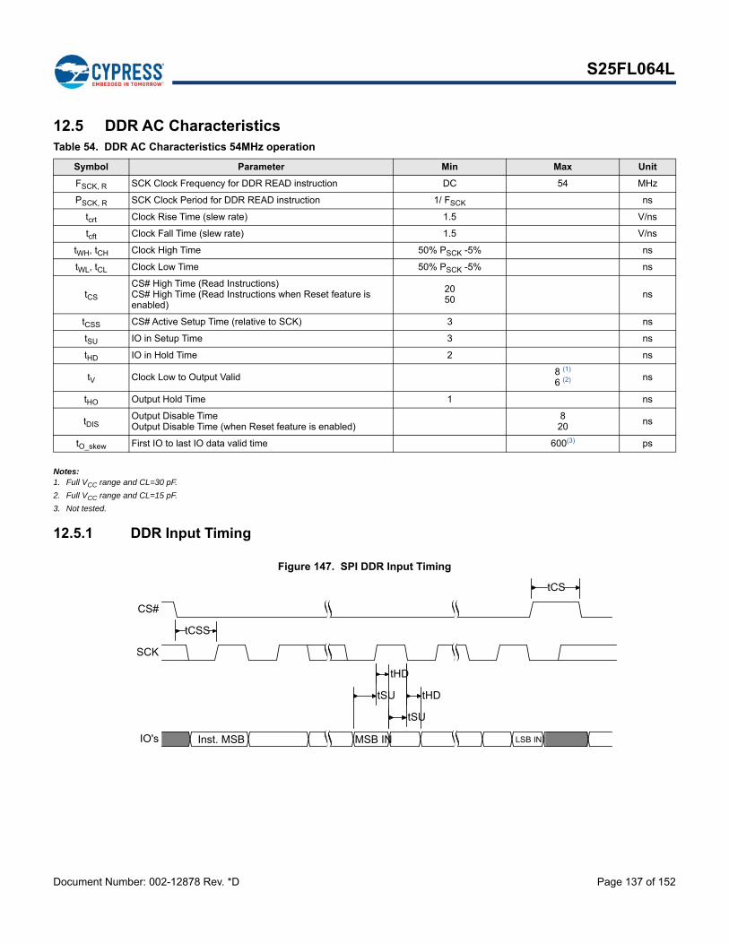
Document Number: 002-12878 Rev. *D Page 137 of 152
S25FL064L
12.5 DDR AC Characteristics
Notes:1. Full VCC range and CL=30 pF.
2. Full VCC range and CL=15 pF.
3. Not tested.
12.5.1 DDR Input Timing
Figure 147. SPI DDR Input Timing
Table 54. DDR AC Characteristics 54MHz operation
Symbol Parameter Min Max Unit
FSCK, R SCK Clock Frequency for DDR READ instruction DC 54 MHz
PSCK, R SCK Clock Period for DDR READ instruction 1/ FSCK ns
tcrt Clock Rise Time (slew rate) 1.5 V/ns
tcft Clock Fall Time (slew rate) 1.5 V/ns
tWH, tCH Clock High Time 50% PSCK -5% ns
tWL, tCL Clock Low Time 50% PSCK -5% ns
tCS CS# High Time (Read Instructions) CS# High Time (Read Instructions when Reset feature is enabled)
2050
ns
tCSS CS# Active Setup Time (relative to SCK) 3 ns
tSU IO in Setup Time 3 ns
tHD IO in Hold Time 2 ns
tV Clock Low to Output Valid 8 (1) 6 (2) ns
tHO Output Hold Time 1 ns
tDISOutput Disable TimeOutput Disable Time (when Reset feature is enabled)
820
ns
tO_skew First IO to last IO data valid time 600(3) ps
CS#
SCK
IO's Inst. MSB MSB IN LSB IN
tCSS
tCS
tSU
tSU
tHD
tHD

Document Number: 002-12878 Rev. *D Page 138 of 152
S25FL064L
12.5.2 DDR Output Timing
Figure 148. SPI DDR Output Timing
12.5.3 DDR Data Valid Timing Using DLP
Figure 149. SPI DDR Data Valid Window
The minimum data valid window (tDV) and tV minimum can be calculated as follows:
tDV = Minimum half clock cycle time (tCLH(1)) - tOTT
(3) - tIO_SKEW (2)
tV _min = tHO + tIO_SKEW + tOTT
Example:
66 MHz clock frequency = 15 ns clock period, DDR operations and duty cycle of 45% or higher
– tCLH = 0.45 x PSCK = 0.45 x 15 ns = 6.75 ns
tOTT calculation(4) is bus impedance of 45 ohm and capacitance of 37 pf, with timing reference of 0.75 VCC, the rise time from 0 to1 or fall time 1 to 0 is 1.4(7) x RC time constant (Tau)(6) = 1.4 x 1.67 ns = 2.34 ns
– tOTT = rise time + fall time = 2.34 ns + 2.34 ns = 4.68 ns.
Data Valid Window
– tDV = tCLH - tIO_SKEW - tOTT = 6.75 ns - 600 ps - 4.68 ns = 1.47 ns
tV Minimum
– tV _min = tHO + tIO_SKEW + tOTT = 1.0 ns + 600 ps + 4.68ns = 5.98ns
Notes1. tCLH is the shorter duration of tCL or tCH.2. tIO_SKEW is the maximum difference (delta) between the minimum and maximum tV (output valid) across all IO signals.3. tOTT is the maximum Output Transition Time from one valid data value to the next valid data value on each IO.4. tOTT is dependent on system level considerations including:
a. Memory device output impedance (drive strength).b. System level parasitics on the IOs (primarily bus capacitance).c. Host memory controller input VIH and VIL levels at which 0 to 1 and 1 to 0 transitions are recognized.d. tOTT is not a specification tested by Cypress, it is system dependent and must be derived by the system designer based on the above considerations.
5. tDV is the data valid window.6. Tau = R (Output Impedance) x C (Load capacitance pF).7. Multiplier of Tau time for voltage to rise to 75% of VCC.
CS#
SCK
IO's MSB LSB
tCS
tVtV tDIStHO
SCK
IO Slow
IO Fast
IO_valid
Slow D1 Slow D2
Fast D1 Fast D2
D1 D2
tV
tIO_SKEW
tDV
tCL tCH
tOTT
pSCK
tHO
tV_min
tV

Document Number: 002-12878 Rev. *D Page 139 of 152
S25FL064L
12.6 Embedded Algorithm Performance Tables
Notes:1. Typical program and erase times assume the following conditions: 25°C, VCC = 3.0 V; checkerboard data pattern.
2. The programming time for any OTP programming command is the same as tPP. This includes IRPP 2Fh, PASSP E8h and PDLRNV 43h.
Table 55. Program and Erase Performance
Symbol Parameter Min Typ (1) Max Unit
tW Non-volatile Register Write Time 220 1200 ms
tPP Page Programming (256 Bytes) 450 1350 µs
tBP1 Byte Programming (First Byte) 75 90 µs
tBP2 Additional Byte Programming (After First Byte)() 10 30 µs
tSE Sector Erase Time (4KB physical sectors) 65 320 ms
tHBE Half Block Erase Time (32KB physical sectors) 300 600 ms
tBE Block Erase Time (64KB physical sectors) 450 1150 ms
tCE Chip Erase Time (S25FL064L) 55 150 sec
Table 56. Program or Erase Suspend AC Parameters
Parameter Typical Max Unit Comments
Suspend Latency (tSL) 40 µs The time from Suspend command until the WIP bit is
0.
Resume to next Suspend (tRNS) 100 µs Is the time needed to issue the next Suspend command.

Document Number: 002-12878 Rev. *D Page 140 of 152
S25FL064L
13. Ordering InformationThe ordering part number is formed by a valid combination of the following:
Valid Combinations — StandardValid Combinations list configurations planned to be supported in volume for this device. Consult your local sales office to confirm availability of specific valid combinations and to check on newly released combinations.
Table 57. Valid Combinations — Standard
S25FL 064 L AB M F I 00 1Packing Type0 = Tray 1 = Tube3 = 13” Tape and Reel
Model Number (Additional Ordering Options)00 = SOIC16 (300 mil) 01 = SOIC8 (208 mil) / 8-contact WSON footprint02 = 5x5 ball BGA footprint03 = 4x6 ball BGA footprint04 = USON (4 x 4mm)
Temperature RangeI = Industrial (–40°C to +85°C)V = Industrial Plus (–40°C to +105°C)A = Automotive, AEC-Q100 Grade 3 (–40°C to +85°C)B = Automotive, AEC-Q100 Grade 2 (–40°C to +105°C)M = Automotive, AEC-Q100 Grade 1 (–40°C to +125°C)
Package MaterialsF = Halogen free, Lead (Pb)-free H = Low-Halogen, Lead (Pb)-free
Package TypeM = 8-Lead SOIC / 16-Lead SOICN = USON 4 x 4 mm / WSON 5 x 6 mmB = 24-ball BGA 6 x 8 mm package, 1.00 mm pitch
SpeedAB = 108 MHz SDR and 54 MHz DDR
Device TechnologyL = Floating Gate Process Technology
Density064 = 64 Mb
Device FamilyS25FL Cypress Memory 3.0 Volt-only, SPI Flash Memory
Valid Combinations — Standard
Base Ordering Part Number
Speed Option
Package and Temperature
Model Number Packing Type Package Marking
S25FL064L
AB MFI, MFV 00, 01 0, 1, 3 FL064L + (Temp) + F + (Model Number)
AB NFI, NFV 01, 04 0, 1, 3 FL064L + (Temp) + F + (Model Number)
AB BHI, BHV 02, 03 0, 3 FL064L + (Temp) + H + (Model Number)

Document Number: 002-12878 Rev. *D Page 141 of 152
S25FL064L
Valid Combinations — Automotive Grade / AEC-Q100The table below lists configurations that are Automotive Grade / AEC-Q100 qualified and are planned to be available in volume. The table will be updated as new combinations are released. Consult your local sales representative to confirm availability of specific combinations and to check on newly released combinations.
Production Part Approval Process (PPAP) support is only provided for AEC-Q100 grade products.
Products to be used in end-use applications that require ISO/TS-16949 compliance must be AEC-Q100 grade products in combination with PPAP. Non–AEC-Q100 grade products are not manufactured or documented in full compliance with ISO/TS-16949 requirements.
AEC-Q100 grade products are also offered without PPAP support for end-use applications that do not require ISO/TS-16949 compliance.
Table 58. Valid Combinations — Automotive Grade / AEC-Q100
Valid Combinations - Automotive Grade / AEC-Q100
Base Ordering Part Number
Speed Option
Package and Temperature
Model Number Packing Type Package Marking
S25FL064L
AB MFA, MFB, MFM 00, 01 0, 1, 3 FL064L + (Temp) + F + (Model Number)
AB NFA, NFB, NFM 01, 04 0, 1, 3 FL064L + (Temp) + F + (Model Number)
AB BHA, BHB, BHM 02, 03 0, 3 FL064L + (Temp) + H + (Model Number)

Document Number: 002-12878 Rev. *D Page 142 of 152
S25FL064L
14. Physical Diagrams
14.1 SOIC 8-Lead, 208 mil Body Width (SOC008)
SHEET OF
REVSPEC NO.THIS DRAWING CONTAINS INFORMATION WHICH IS THE PROPRIETARY PROPERTY OF CYPRESSSEMICONDUCTOR CORPORATION. THIS DRAWING IS RECEIVED IN CONFIDENCE AND ITS CONTENTSMAY NOT BE DISCLOSED WITHOUT WRITTEN CONSENT OF CYPRESS SEMICONDUCTOR CORPORATION.
CYPRESS
TITLE
SCALE :
Company Confidential
PACKAGECODE(S)
DRAWN BY
APPROVED BY
DATE
DATE
5.28 BSCD
0.51
20
10
0
N
L1
L2
E1
L
e
E
15°
0°
5°
8°
0.76
5.28 BSC
8.00 BSC
1.36 REF
0.25 BSC
8
1.27 BSC
1.70
1.75
0.05
0.33
0.36
0.15
0.19
c1
c
b1
b
A2
A1
A
1.90
2.16
0.25
0.48
0.46
0.20
0.24
0-8° REF
2. DIMENSIONING AND TOLERANCING PER ASME Y14.5M - 1994.3. DIMENSION D DOES NOT INCLUDE MOLD FLASH, PROTRUSIONS OR GATE BURRS.
END. DIMENSION E1 DOES NOT INCLUDE INTERLEAD FLASH OR PROTRUSION.INTERLEAD FLASH OR PROTRUSION SHALL NOT EXCEED 0.25 mm PER SIDE.
1. ALL DIMENSIONS ARE IN MILLIMETERS.
NOTES:
D AND E1 DIMENSIONS ARE DETERMINED AT DATUM H.
FLASH, BUT INCLUSIVE OF ANY MISMATCH BETWEEN THE TOP AND BOTTOM OFEXCLUSIVE OF MOLD FLASH, TIE BAR BURRS, GATE BURRS AND INTERLEAD
4. THE PACKAGE TOP MAY BE SMALLER THAN THE PACKAGE BOTTOM. DIMENSIONS
5. DATUMS A AND B TO BE DETERMINED AT DATUM H.6. "N" IS THE MAXIMUM NUMBER OF TERMINAL POSITIONS FOR THE SPECIFIED
7. THE DIMENSIONS APPLY TO THE FLAT SECTION OF THE LEAD BETWEEN 0.10 TO
MAXIMUM MATERIAL CONDITION. THE DAMBAR CANNOT BE LOCATED ON THE
8. DIMENSION "b" DOES NOT INCLUDE DAMBAR PROTRUSION. ALLOWABLE DAMBAR
LOWER RADIUS OF THE LEAD FOOT.
IDENTIFIER MUST BE LOCATED WITHIN THE INDEX AREA INDICATED.9. THIS CHAMFER FEATURE IS OPTIONAL. IF IT IS NOT PRESENT, THEN A PIN 1
10. LEAD COPLANARITY SHALL BE WITHIN 0.10 mm AS MEASURED FROM THE
MOLD FLASH, PROTRUSIONS OR GATE BURRS SHALL NOT EXCEED 0.15 mm PER
D AND E1 ARE DETERMINED AT THE OUTMOST EXTREMES OF THE PLASTIC BODY
0.25 mm FROM THE LEAD TIP.
PROTRUSION SHALL BE 0.10 mm TOTAL IN EXCESS OF THE "b" DIMENSION AT
THE PLASTIC BODY.
PACKAGE LENGTH.
SEATING PLANE.
DIMENSIONSSYMBOL
MIN. NOM. MAX.
-
-
-
-
-
-
-
-
-
-
KOTA
BESY
18-JUL-16
18-JUL-16**
1 2TO FIT
SOC008 002-15548
PACKAGE OUTLINE, 8 LEAD SOIC5.28X5.28X2.16 MM SOC008

Document Number: 002-12878 Rev. *D Page 143 of 152
S25FL064L
14.2 SOIC 16-Lead, 300 mil Body Width (SO3016)
SHEET OF
REVSPEC NO.THIS DRAWING CONTAINS INFORMATION WHICH IS THE PROPRIETARY PROPERTY OF CYPRESSSEMICONDUCTOR CORPORATION. THIS DRAWING IS RECEIVED IN CONFIDENCE AND ITS CONTENTSMAY NOT BE DISCLOSED WITHOUT WRITTEN CONSENT OF CYPRESS SEMICONDUCTOR CORPORATION.
CYPRESS
TITLE
SCALE :
Company Confidential
PACKAGECODE(S)
DRAWN BY
APPROVED BY
DATE
DATE
0.33 C
0.25 M DC A-B
0.20 C A-B
0.10 C
0.10 C
0.10 C D2X
2. DIMENSIONING AND TOLERANCING PER ASME Y14.5M - 1994.3. DIMENSION D DOES NOT INCLUDE MOLD FLASH, PROTRUSIONS OR GATE BURRS.
END. DIMENSION E1 DOES NOT INCLUDE INTERLEAD FLASH OR PROTRUSION.INTERLEAD FLASH OR PROTRUSION SHALL NOT EXCEED 0.25 mm PER SIDE.
1. ALL DIMENSIONS ARE IN MILLIMETERS.
NOTES:
D AND E1 DIMENSIONS ARE DETERMINED AT DATUM H.
FLASH, BUT INCLUSIVE OF ANY MISMATCH BETWEEN THE TOP AND BOTTOM OFEXCLUSIVE OF MOLD FLASH, TIE BAR BURRS, GATE BURRS AND INTERLEAD
4. THE PACKAGE TOP MAY BE SMALLER THAN THE PACKAGE BOTTOM. DIMENSIONS
5. DATUMS A AND B TO BE DETERMINED AT DATUM H.6. "N" IS THE MAXIMUM NUMBER OF TERMINAL POSITIONS FOR THE SPECIFIED
7. THE DIMENSIONS APPLY TO THE FLAT SECTION OF THE LEAD BETWEEN 0.10 TO
MAXIMUM MATERIAL CONDITION. THE DAMBAR CANNOT BE LOCATED ON THE
8. DIMENSION "b" DOES NOT INCLUDE DAMBAR PROTRUSION. ALLOWABLE DAMBAR
LOWER RADIUS OF THE LEAD FOOT.
IDENTIFIER MUST BE LOCATED WITHIN THE INDEX AREA INDICATED.9. THIS CHAMFER FEATURE IS OPTIONAL. IF IT IS NOT PRESENT, THEN A PIN 1
10. LEAD COPLANARITY SHALL BE WITHIN 0.10 mm AS MEASURED FROM THE
h
0
D
L2N
e
A1
b
c
E
E1
A
0.75
10.30 BSC
1.27 BSC
0.30
10.30 BSC
0.33
0°0.25
16
0.20
7.50 BSC
0.10
0.31
8°
0.51
2.652.35
A2 2.05 2.55
b1 0.27 0.48
0.300.20c1
L10.40L 1.27
1.40 REF0.25 BSC
0 5° 15°0 0°
12 -
DIMENSIONSSYMBOL
MIN. NOM. MAX.
----
-------
-
MOLD FLASH, PROTRUSIONS OR GATE BURRS SHALL NOT EXCEED 0.15 mm PER
D AND E1 ARE DETERMINED AT THE OUTMOST EXTREMES OF THE PLASTIC BODY
0.25 mm FROM THE LEAD TIP.
PROTRUSION SHALL BE 0.10 mm TOTAL IN EXCESS OF THE "b" DIMENSION AT
THE PLASTIC BODY.
PACKAGE LENGTH.
SEATING PLANE.
SO3016KOTA
BESY
24-OCT-16
24-OCT-16*A002-15547
PACKAGE OUTLINE, 16 LEAD SOIC
1 2TO FIT
10.30X7.50X2.65 MM SO3016/SL3016/SS3016
SL3016 SS3016

Document Number: 002-12878 Rev. *D Page 144 of 152
S25FL064L
14.3 USON 4 x 4 mm (UNF008)
SHEET OF
REVSPEC NO.THIS DRAWING CONTAINS INFORMATION WHICH IS THE PROPRIETARY PROPERTY OF CYPRESSSEMICONDUCTOR CORPORATION. THIS DRAWING IS RECEIVED IN CONFIDENCE AND ITS CONTENTSMAY NOT BE DISCLOSED WITHOUT WRITTEN CONSENT OF CYPRESS SEMICONDUCTOR CORPORATION.
CYPRESS
TITLE
SCALE :
Company Confidential
PACKAGECODE(S)
DRAWN BY
APPROVED BY
DATE
DATE
JEDEC SPECIFICATION NO. REF: N/A
COPLANARITY ZONE APPLIES TO THE EXPOSED HEAT SINKPIN #1 ID ON TOP WILL BE LOCATED WITHIN THE INDICATED ZONE.
DIMENSION "b" APPLIES TO METALLIZED TERMINAL AND IS MEASURED N IS THE TOTAL NUMBER OF TERMINALS. ALL DIMENSIONS ARE IN MILLIMETERS.
NOTES:
5.4.
1.
3.2.
6.
7.
THE OPTIONAL RADIUS ON THE OTHER END OF THE TERMINAL, THE DIMENSION "b" SHOULD NOT BE MEASURED IN THAT RADIUS AREA.ND REFERS TO THE NUMBER OF TERMINALS ON D SIDE.
84
0.80 BSC.
0.30
4.00 BSC4.00 BSC
2.303.00
0.20
0.550.035
0.40
A1
K
A
E2DE
D2b
LNDNe
0.00
2.90
0.50
2.200.25
0.35
3.10
0.050.60
2.400.35
0.45
A3 0.152 REF
DIMENSIONSSYMBOL
MIN. NOM. MAX.
BETWEEN 0.15 AND 0.30mm FROM TERMINAL TIP. IF THE TERMINAL HAS
SLUG AS WELL AS THE TERMINALS.
- -
*A1 2
KOTA
BESY
28-NOV-16
28-NOV-16
UNF008 002-16243
PACKAGE OUTLINE, 8 LEAD DFN4.0X4.0X0.6 MM UNF008, 2.3X3.0 MM EPAD (SAWN)
TO FIT
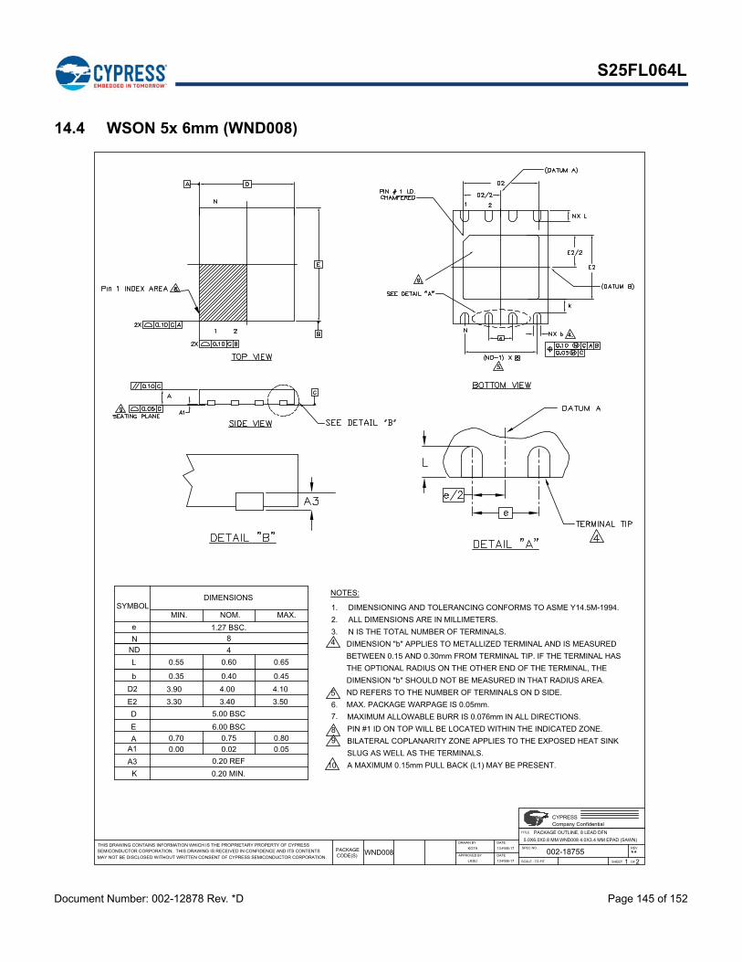
Document Number: 002-12878 Rev. *D Page 145 of 152
S25FL064L
14.4 WSON 5x 6mm (WND008)
SHEET OF
REVSPEC NO.THIS DRAWING CONTAINS INFORMATION WHICH IS THE PROPRIETARY PROPERTY OF CYPRESSSEMICONDUCTOR CORPORATION. THIS DRAWING IS RECEIVED IN CONFIDENCE AND ITS CONTENTSMAY NOT BE DISCLOSED WITHOUT WRITTEN CONSENT OF CYPRESS SEMICONDUCTOR CORPORATION.
CYPRESS
TITLE
SCALE :
Company Confidential
PACKAGECODE(S)
DRAWN BY
APPROVED BY
DATE
DATE
A MAXIMUM 0.15mm PULL BACK (L1) MAY BE PRESENT.
BILATERAL COPLANARITY ZONE APPLIES TO THE EXPOSED HEAT SINKPIN #1 ID ON TOP WILL BE LOCATED WITHIN THE INDICATED ZONE.MAXIMUM ALLOWABLE BURR IS 0.076mm IN ALL DIRECTIONS.
DIMENSION "b" APPLIES TO METALLIZED TERMINAL AND IS MEASURED N IS THE TOTAL NUMBER OF TERMINALS. ALL DIMENSIONS ARE IN MILLIMETERS. DIMENSIONING AND TOLERANCING CONFORMS TO ASME Y14.5M-1994.
NOTES:
MAX. PACKAGE WARPAGE IS 0.05mm.
8
7.6.5
2.
43.
1.
9
10
THE OPTIONAL RADIUS ON THE OTHER END OF THE TERMINAL, THE DIMENSION "b" SHOULD NOT BE MEASURED IN THAT RADIUS AREA.ND REFERS TO THE NUMBER OF TERMINALS ON D SIDE.
84
1.27 BSC.
0.40
6.00 BSC5.00 BSC
4.003.40
0.20 MIN.
0.750.02
0.60
A1
K
A
E2DE
D2b
LNDNe
0.00
3.30
0.70
3.900.35
0.55
3.50
0.050.80
4.100.45
0.65
A3 0.20 REF
DIMENSIONSSYMBOL
MIN. NOM. MAX.
BETWEEN 0.15 AND 0.30mm FROM TERMINAL TIP. IF THE TERMINAL HAS
SLUG AS WELL AS THE TERMINALS.
KOTA
LKSU
13-FEB-17
13-FEB-17**
1 2TO FIT
WND008 002-18755
PACKAGE OUTLINE, 8 LEAD DFN5.0X6.0X0.8 MM WND008 4.0X3.4 MM EPAD (SAWN)

Document Number: 002-12878 Rev. *D Page 146 of 152
S25FL064L
14.5 Ball Grid Array, 24-ball 6 x 8 mm (FAB024)
SHEET OF
REVSPEC NO.THIS DRAWING CONTAINS INFORMATION WHICH IS THE PROPRIETARY PROPERTY OF CYPRESSSEMICONDUCTOR CORPORATION. THIS DRAWING IS RECEIVED IN CONFIDENCE AND ITS CONTENTSMAY NOT BE DISCLOSED WITHOUT WRITTEN CONSENT OF CYPRESS SEMICONDUCTOR CORPORATION.
CYPRESS
TITLE
SCALE :
Company Confidential
PACKAGECODE(S)
DRAWN BY
APPROVED BY
DATE
DATE
METALLIZED MARK INDENTATION OR OTHER MEANS.
A1 CORNER TO BE IDENTIFIED BY CHAMFER, LASER OR INK MARK,
N IS THE NUMBER OF POPULATED SOLDER BALL POSITIONS FOR MATRIX SIZE MD X ME.
WHEN THERE IS AN EVEN NUMBER OF SOLDER BALLS IN THE OUTER ROW, "SD" = eD/2 AND
WHEN THERE IS AN ODD NUMBER OF SOLDER BALLS IN THE OUTER ROW, "SD" OR "SE" = 0.
POSITION OF THE CENTER SOLDER BALL IN THE OUTER ROW.
"SD" AND "SE" ARE MEASURED WITH RESPECT TO DATUMS A AND B AND DEFINE THE
SYMBOL "ME" IS THE BALL MATRIX SIZE IN THE "E" DIRECTION.
SYMBOL "MD" IS THE BALL MATRIX SIZE IN THE "D" DIRECTION.
e REPRESENTS THE SOLDER BALL GRID PITCH.
DIMENSION "b" IS MEASURED AT THE MAXIMUM BALL DIAMETER IN A PLANE
BALL POSITION DESIGNATION PER JEP95, SECTION 3, SPP-020.
DIMENSIONING AND TOLERANCING METHODS PER ASME Y14.5M-1994.
"+" INDICATES THE THEORETICAL CENTER OF DEPOPULATED BALLS.8.
9.
7
ALL DIMENSIONS ARE IN MILLIMETERS.
PARALLEL TO DATUM C.
5.
6
4.
3.
2.
1.
NOTES:
SD
b
eD
eE
ME
N
0.35
0.00 BSC
1.00 BSC
1.00 BSC
0.40
24
5
0.45
D1
MD
E1
E
D
A
A1 0.20
-
4.00 BSC
4.00 BSC
5
6.00 BSC
8.00 BSC
-
- 1.20
-
SE 0.00 BSC
DIMENSIONSSYMBOL
MIN. NOM. MAX.
"SE" = eE/2.
FAB024KOTA
BESY
18-JUL-16
18-JUL-16**002-15534
PACKAGE OUTLINE, 24 BALL FBGA
1 2TO FIT
8.0X6.0X1.2 MM FAB024

Document Number: 002-12878 Rev. *D Page 147 of 152
S25FL064L
14.6 Ball Grid Array, 24-ball 6 x 8 mm (FAC024)
SHEET OF
REVSPEC NO.THIS DRAWING CONTAINS INFORMATION WHICH IS THE PROPRIETARY PROPERTY OF CYPRESSSEMICONDUCTOR CORPORATION. THIS DRAWING IS RECEIVED IN CONFIDENCE AND ITS CONTENTSMAY NOT BE DISCLOSED WITHOUT WRITTEN CONSENT OF CYPRESS SEMICONDUCTOR CORPORATION.
CYPRESS
TITLE
SCALE :
Company Confidential
PACKAGECODE(S)
DRAWN BY
APPROVED BY
DATE
DATE
METALLIZED MARK INDENTATION OR OTHER MEANS.
A1 CORNER TO BE IDENTIFIED BY CHAMFER, LASER OR INK MARK,
N IS THE NUMBER OF POPULATED SOLDER BALL POSITIONS FOR MATRIX SIZE MD X ME.
WHEN THERE IS AN EVEN NUMBER OF SOLDER BALLS IN THE OUTER ROW, "SD" = eD/2 AND
WHEN THERE IS AN ODD NUMBER OF SOLDER BALLS IN THE OUTER ROW, "SD" OR "SE" = 0.
POSITION OF THE CENTER SOLDER BALL IN THE OUTER ROW.
"SD" AND "SE" ARE MEASURED WITH RESPECT TO DATUMS A AND B AND DEFINE THE
SYMBOL "ME" IS THE BALL MATRIX SIZE IN THE "E" DIRECTION.
SYMBOL "MD" IS THE BALL MATRIX SIZE IN THE "D" DIRECTION.
e REPRESENTS THE SOLDER BALL GRID PITCH.
DIMENSION "b" IS MEASURED AT THE MAXIMUM BALL DIAMETER IN A PLANE
BALL POSITION DESIGNATION PER JEP95, SECTION 3, SPP-020.
DIMENSIONING AND TOLERANCING METHODS PER ASME Y14.5M-1994.
"+" INDICATES THE THEORETICAL CENTER OF DEPOPULATED BALLS.8.
9.
7
ALL DIMENSIONS ARE IN MILLIMETERS.
PARALLEL TO DATUM C.
5.
6
4.
3.
2.
1.
NOTES:
SD
b
eD
eE
ME
N
0.35
0.50 BSC
1.00 BSC
1.00 BSC
0.40
24
4
0.45
D1
MD
E1
E
D
A
A1 0.25
-
5.00 BSC
3.00 BSC
6
6.00 BSC
8.00 BSC
-
- 1.20
-
SE 0.50 BSC
DIMENSIONSSYMBOL
MIN. NOM. MAX.
"SE" = eE/2.
FAC024KOTA
BESY
18-JUL-16
18-JUL-16**002-15535
PACKAGE OUTLINE, 24 BALL FBGA
1 2TO FIT
8.0X6.0X1.2 MM FAC024

Document Number: 002-12878 Rev. *D Page 148 of 152
S25FL064L
15. Other Resources
15.1 Glossary
BCD Binary Coded Decimal. A value in which each 4 bit nibble represents a decimal numeral.
CommandAll information transferred between the host system and memory during one period while CS# is low. This includes the instruction (sometimes called an operation code or opcode) and any required address, mode bits, latency cycles, or data.
DDP Dual Die Package = Two die stacked within the same package to increase the memory capacity of a single package. Often also referred to as a Multi-Chip Package (MCP).
DDR Double Data Rate = When input and output are latched on every edge of SCK.
DIO Dual Input Output
Flash The name for a type of Electrical Erase Programmable Read Only Memory (EEPROM) that erases large blocks of memory bits in parallel, making the erase operation much faster than early EEPROM.
High A signal voltage level ≥ VIH or a logic level representing a binary one (“1”).
InstructionThe 8 bit code indicating the function to be performed by a command (sometimes called an operation code or opcode). The instruction is always the first 8 bits transferred from host system to the memory in any command.
Low A signal voltage level VIL or a logic level representing a binary zero (“0”).
LSB Least Significant Bit = Generally the right most bit, with the lowest order of magnitude value, within a group of bits of a register or data value.
MSBMost Significant Bit = Generally the left most bit, with the highest order of magnitude value, within a group of bits of a register or data value.
N/A Not Applicable. A value is not relevant to situation described.
Non-Volatile No power is needed to maintain data stored in the memory.
OPN Ordering Part Number = The alphanumeric string specifying the memory device type, density, package, factory non-volatile configuration, etc. used to select the desired device.
QIO Quad Input Output Mode
QPI Quad Peripheral Interface
Page 256 Byte length and aligned group of data.
PCB Printed Circuit Board
Register Bit References In the format: Register_name[bit_number] or Register_name[bit_range_MSB: bit_range_LSB]
Sector Erase unit size; depending on device model and sector location this may be 4KBytes, 32KBytes or 64KBytes
SDR Single Data Rate = When input is latched on the rising edge and output on the falling edge of SCK.
Write
An operation that changes data within volatile or non-volatile registers bits or non-volatile Flash memory. When changing non-volatile data, an erase and reprogramming of any unchanged non-volatile data is done, as part of the operation, such that the non-volatile data is modified by the write operation, in the same way that volatile data is modified – as a single operation. The non-volatile data appears to the host system to be updated by the single write command, without the need for separate commands for erase and reprogram of adjacent, but unaffected data.

Document Number: 002-12878 Rev. *D Page 149 of 152
S25FL064L
15.2 Link to Cypress Flash Roadmapwww.cypress.com/Flash-Roadmap
15.3 Link to Softwarewww.cypress.com/software-and-drivers-cypress-flash-memory
15.4 Link to Application Noteswww.cypress.com/cypressappnotes

Document Number: 002-12878 Rev. *D Page 150 of 152
S25FL064L
16. Document History
Document Title: S25FL064L, 64-Mbit (8-Mbyte) 3.0 V FL-L SPI Flash MemoryDocument Number: 002-12878
Rev. ECN No. Orig. of Change
Submission Date Description of Change
** 5364133 BWHA 07/27/2016 Initial release
*A 5449347 BWHA 09/26/2016
Changed status from Advance to Preliminary.
Updated Features:
Added Automotive Grade related information.
Updated Data Integrity:
Updated Data Retention:
Updated Table 37.
Updated Ordering Information:
Updated details corresponding to “01” under “Model Number (Additional Ordering Options)”.
Added Automotive Grade related information.
Added Valid Combinations — Automotive Grade / AEC-Q100.
Updated Physical Diagrams:
updated Package Drawings to Cypress release.
*B 5581541 BWHA 01/13/2017
Updated Data Retention:
Added Cypress application notes website URL.
Updated Power-Up / Power-Down Voltage and Timing:
Updated Table 46:
Added notes for VCC (cut-off) and VCC (low) min values.
Updated DC Characteristics: Added notes for IPOR in-rush current for all temperature ranges.POR current for typical and maximum reduced.
Updated Ordering Information:
Added “04” under “Model Number”.
Updated Table 32, FL-L Family Command Set (sorted by function) on page 60:
Updated DDRQIOR and 4DDRQIOR Max Frequency.
Updated Table 33, Register Address Map on page 76:
Updated Byte Address 00003B Register Name
Datasheet converted from Preliminary to Final

Document Number: 002-12878 Rev. *D Page 151 of 152
S25FL064L
*C 5737077 ECAO 05/15/2017
Removed Extended Temperature Range Options (–40°C to +125°C) from datasheet.
Updated Table 1, Cypress SPI Families Comparison on page 4
Added Figure 1, 16-Lead SOIC Package (SO3016), Top View on page 6
Updated Table 32, FL-L Family Command Set (sorted by function) on page 60:
Corrected Command Description for RDSR2 to Read Status Register 2.
Updated Section 8.3, Register Access Commands on page 67:
Updated Section 8.3.2, Read Status Register 2 (RDSR2 07h) on page 67:
Corrected all mention of Status Register 1 to Status Register 2.
Updated Table 40, Basic SPI Flash Parameter, JEDEC SFDP Rev B on page 116:
Corrected Bit 22 description at address 02h from “DOR” to “QOR”
Corrected data at address 3Dh from 60h to 50h.
Updated Section 13., Ordering Information on page 140:
Added WSON 5 x 6mm package option.
Added 16-Lead SOIC package option.
Updated Table 57, Valid Combinations — Standard on page 140
Updated Table 58, Valid Combinations — Automotive Grade / AEC-Q100 on page 141:
Removed Model 04 option for MF* Package and Temperature option.
Added Model 01 option for 16-Lead SOIC package.
Added Section 14.2, SOIC 16-Lead, 300 mil Body Width (SO3016) on page 143
Added Section 14.4, WSON 5x 6mm (WND008) on page 145.
Updated Cypress logo, Sales page, and Copyright information.
*D 6090046 BWHA 04/04/2018
Updated 12.5.3, DDR Data Valid Timing Using DLP on page 138: Updated Figure 74, DDR Quad I/O Read Initial Access on page 88
Updated Figure 75, DDR Quad I/O Read Initial Access QPI Mode on page 88
Updated Figure 76, Continuous DDR Quad I/O Read Subsequent Access on page 88
Updated Figure 22, DDR Quad I/O Read Command on page 21 and Figure 23, DDR Quad I/O Read Command QPI Mode on page 21
Updated Table 43, Unique Device ID on page 122Updated Table 44, Latchup Specification on page 123
Updated Table 47, DC Characteristics — Operating Temperature Range –40°C to +85°C on page 127 improved ICC & ISB current specifications.
Updated Table 48, DC Characteristics — Operating Temperature Range –40°C to +105°C on page 128 improved ICC & ISB current specifications.
Updated Table 49, DC Characteristics — Operating Temperature Range –40°C to +125°C on page 129 improved ICC & ISB current specifications.
Document Title: S25FL064L, 64-Mbit (8-Mbyte) 3.0 V FL-L SPI Flash MemoryDocument Number: 002-12878
Rev. ECN No. Orig. of Change
Submission Date Description of Change

Document Number: 002-12878 Rev. *D Revised April 04, 2018 Page 152 of 152
© Cypress Semiconductor Corporation, 2016-2018. This document is the property of Cypress Semiconductor Corporation and its subsidiaries, including Spansion LLC ("Cypress"). This document,including any software or firmware included or referenced in this document ("Software"), is owned by Cypress under the intellectual property laws and treaties of the United States and other countriesworldwide. Cypress reserves all rights under such laws and treaties and does not, except as specifically stated in this paragraph, grant any license under its patents, copyrights, trademarks, or otherintellectual property rights. If the Software is not accompanied by a license agreement and you do not otherwise have a written agreement with Cypress governing the use of the Software, then Cypresshereby grants you a personal, non-exclusive, nontransferable license (without the right to sublicense) (1) under its copyright rights in the Software (a) for Software provided in source code form, tomodify and reproduce the Software solely for use with Cypress hardware products, only internally within your organization, and (b) to distribute the Software in binary code form externally to end users(either directly or indirectly through resellers and distributors), solely for use on Cypress hardware product units, and (2) under those claims of Cypress's patents that are infringed by the Software (asprovided by Cypress, unmodified) to make, use, distribute, and import the Software solely for use with Cypress hardware products. Any other use, reproduction, modification, translation, or compilationof the Software is prohibited.
TO THE EXTENT PERMITTED BY APPLICABLE LAW, CYPRESS MAKES NO WARRANTY OF ANY KIND, EXPRESS OR IMPLIED, WITH REGARD TO THIS DOCUMENT OR ANY SOFTWAREOR ACCOMPANYING HARDWARE, INCLUDING, BUT NOT LIMITED TO, THE IMPLIED WARRANTIES OF MERCHANTABILITY AND FITNESS FOR A PARTICULAR PURPOSE. No computingdevice can be absolutely secure. Therefore, despite security measures implemented in Cypress hardware or software products, Cypress does not assume any liability arising out of any security breach,such as unauthorized access to or use of a Cypress product. In addition, the products described in these materials may contain design defects or errors known as errata which may cause the productto deviate from published specifications. To the extent permitted by applicable law, Cypress reserves the right to make changes to this document without further notice. Cypress does not assume anyliability arising out of the application or use of any product or circuit described in this document. Any information provided in this document, including any sample design information or programmingcode, is provided only for reference purposes. It is the responsibility of the user of this document to properly design, program, and test the functionality and safety of any application made of thisinformation and any resulting product. Cypress products are not designed, intended, or authorized for use as critical components in systems designed or intended for the operation of weapons, weaponssystems, nuclear installations, life-support devices or systems, other medical devices or systems (including resuscitation equipment and surgical implants), pollution control or hazardous substancesmanagement, or other uses where the failure of the device or system could cause personal injury, death, or property damage ("Unintended Uses"). A critical component is any component of a deviceor system whose failure to perform can be reasonably expected to cause the failure of the device or system, or to affect its safety or effectiveness. Cypress is not liable, in whole or in part, and youshall and hereby do release Cypress from any claim, damage, or other liability arising from or related to all Unintended Uses of Cypress products. You shall indemnify and hold Cypress harmless fromand against all claims, costs, damages, and other liabilities, including claims for personal injury or death, arising from or related to any Unintended Uses of Cypress products.
Cypress, the Cypress logo, Spansion, the Spansion logo, and combinations thereof, WICED, PSoC, CapSense, EZ-USB, F-RAM, and Traveo are trademarks or registered trademarks of Cypress inthe United States and other countries. For a more complete list of Cypress trademarks, visit cypress.com. Other names and brands may be claimed as property of their respective owners.
S25FL064L
Sales, Solutions, and Legal Information
Worldwide Sales and Design Support
Cypress maintains a worldwide network of offices, solution centers, manufacturer’s representatives, and distributors. To find the office closest to you, visit us at Cypress Locations.
Products
Arm® Cortex® Microcontrollers cypress.com/arm
Automotive cypress.com/automotive
Clocks & Buffers cypress.com/clocks
Interface cypress.com/interface
Internet of Things cypress.com/iot
Memory cypress.com/memory
Microcontrollers cypress.com/mcu
PSoC cypress.com/psoc
Power Management ICs cypress.com/pmic
Touch Sensing cypress.com/touch
USB Controllers cypress.com/usb
Wireless Connectivity cypress.com/wireless
PSoC® Solutions
PSoC 1 | PSoC 3 | PSoC 4 | PSoC 5LP | PSoC 6 MCU
Cypress Developer Community
Community | Projects | Video | Blogs | Training | Components
Technical Support
cypress.com/support

Mouser Electronics
Authorized Distributor
Click to View Pricing, Inventory, Delivery & Lifecycle Information: Cypress Semiconductor:
S25FL064LABMFB010 S25FL064LABBHV023 S25FL064LABBHN030 S25FL064LABMFI011
S25FL064LABNFV043 S25FL064LABBHN020 S25FL064LABMFN010 S25FL064LABMFV013
S25FL064LABBHN033 S25FL064LABNFN040 S25FL064LABBHI023 S25FL064LABMFB013 S25FL064LABBHV030
S25FL064LABBHI030 S25FL064LABMFN013 S25FL064LABBHV020 S25FL064LABBHN023
S25FL064LABNFN043 S25FL064LABNFI040 S25FL064LABMFM010 S25FL064LABBHI020 S25FL064LABNFI043
S25FL064LABMFV010 S25FL064LABBHI033 S25FL064LABBHV033 S25FL064LABMFI010 S25FL064LABMFI013
S25FL064LABNFV040 S25FL064LABMFM013 S25FL064LABNFI041 S25FL064LABMFA013 S25FL064LABMFA010
S25FL064LABNFM010 S25FL064LABBHB030 S25FL064LABNFV013 S25FL064LABBHA023
S25FL064LABBHB023 S25FL064LABNFM011 S25FL064LABNFM043 S25FL064LABNFM041
S25FL064LABNFB043 S25FL064LABNFI013 S25FL064LABNFM013 S25FL064LABNFA043 S25FL064LABNFB040
S25FL064LABNFI011 S25FL064LABBHB020 S25FL064LABNFA010 S25FL064LABMFB011 S25FL064LABNFB010
S25FL064LABBHA020 S25FL064LABMFM011 S25FL064LABNFI010 S25FL064LABNFB013 S25FL064LABMFA011
S25FL064LABBHB033 S25FL064LABNFA040 S25FL064LABNFA013 S25FL064LABNFB011
S25FL064LABNFV011 S25FL064LABNFA011 S25FL064LABNFV010 S25FL064LABNFM040 S25FL064LABMFV003
S25FL064LABMFI003 S25FL064LABMFA003 S25FL064LABMFM003 S25FL064LABMFB000
S25FL064LABMFB003 S25FL064LABMFV001 S25FL064LABMFI001 S25FL064LABMFI000 S25FL064LABMFM001
S25FL064LABMFM000 S25FL064LABMFA001 S25FL064LABMFB001 S25FL064LABMFV000
S25FL064LABMFA000