numerical and experimental analysis of …progress in electromagnetics research, vol. 122, 223{244,...
TRANSCRIPT
Progress In Electromagnetics Research, Vol. 122, 223–244, 2012
NUMERICAL AND EXPERIMENTAL ANALYSIS OFEMI-INDUCED NOISE IN RC PHASE SHIFT OSCILLA-TOR
H.-C. Tsai*
Department of Electronic Engineering, Chen-Shiu University, No. 840,Chengcing Road, Neausong District, Kaohsiung 83305, Taiwan
Abstract—Electromagnetic interference (EMI) has an adverse effecton the performance of electronic circuit communication systems. Thisstudy derives a series of equations to analyze the effects of the EMIinduced in a conducting wire on the noise spectrum of a RC Phase ShiftOscillator (RCPSO). It is shown that the extent to which EMI affectsthe RCPSO depends on the interference power, interference frequency,induced power, output resistance of oscillator circuit, and parasiticcapacitance. Specifically, higher EMI frequencies and amplitudes havea greater effect on the RCPSO output. The results presented in thisstudy are in good agreement with those predicted from general EMItheory.
1. INTRODUCTION
For many nations, the state of the domestic electronics industryprovides a good indicator of the nation’s general economic wellbeing.Thus, the manufacture of electronic components is a central element inthe development plans of many governments around the world. Withthe proliferation of wireless and electronic devices in recent years, theenvironment is becoming increasingly saturated with electromagneticwaves. Whilst some of these waves, termed as “signals”, are necessaryand useful in that they fulfill a specific design purpose, others areundesirable since they interfere with nearby electrical or electronicdevices. For example, a cell phone used next to a computer maycause a distortion of the image on the screen or a static blast
Received 1 October 2011, Accepted 7 November 2011, Scheduled 17 November 2011* Corresponding author: Han-Chang Tsai ([email protected]).

224 Tsai
from the speakers. Thus, when designing electronic components,the aim is to develop high quality products which perform reliablyin electromagnetic interference (EMI) contaminated environmentswithout interfering with neighboring devices themselves.
The literature contains a large number of studies on the mitigationof EMI effects [1–15]. For example, in [2], a method was proposedfor detecting EMI-induced errors in radio frequency integrated circuit(RFIC) autotest-equipment (ATE) and for recovering these errorsvia a retest procedure. In a recent study [6], it was shown thatexternal EMI can still interfere with shielded active circuits at certainfrequencies of the interference source. In [9], the authors presenteda new method for calibrating non-stationary electromagnetic fieldmeasurements based on the double modulation of a standard excitingsource. In power substations, the EMI generated during the switchingof disconnectors and circuit breakers can cause nearby electronicequipment to malfunction or fail if it is not adequately shielded.Consequently, the authors in [10] performed a finite element analysisof three common shielding and filtering methods, namely metallicchannel, braided cable and additional cable. In [10], the authorsexamined two un-resolved problems in the high-tech industry field,namely the interpretation of EMI laboratory correlation studies andthe margin below the CISPR 22 limit at which EMI compatibilitycompliance can still be achieved.
However, modern electrical circuits comprise an ever increasingnumber of electronic components packaged within devices of everreducing size. The high transmission speeds and operating frequenciesof these circuits, combined with an increasing wiring density, not onlyincrease the risk of the circuit interfering with other electronic devices,but also increase the susceptibility of the device to EMI. As a result, itis essential that the effects of EMI on common electronic componentsare thoroughly understood such that appropriate mitigating measurescan be taken.
Accordingly, this study examines the effect of EMI on the noisespectrum of an RC Phase Shift Oscillator (RCPSO), a wavelength-based device with many applications in the electronics field. Ina normal indoor environment, the intensity of the low frequencyelectromagnetic waves is greater than that of the high frequency waves,i.e., 0.03µT and 0.0067µT, respectively (as measured by the currentauthors using CA40/43 instrumentation (Chauvin Arnoux, France)).Therefore, in analyzing the effects of EMI on the RCPSO, the presentanalysis focuses specifically on low frequency EMI.

Progress In Electromagnetics Research, Vol. 122, 2012 225
2. EXPERIMENTS
Figure 1 shows the experimental setup used to measure the interferencenoise spectrum of the RCPSO. As shown, a conducting wire (CW)was positioned in the air gap of a ferromagnetic toroid wrappedin a current-carrying coil. During the experiments, an EMI sourcewas simulated by applying a voltage across points A and B of thecoil, causing a current to flow in the CW. The resulting magneticfield induced in the air gap was amplified by a 74 dB low-noise pre-amplifier such that it could be detected by an oscilloscope and wasthen connected in series with the RCPSO circuit. In other words,the EMI interference was detected initially as radiated noise and wasthen coupled with the RCPSO circuit as conducted noise. The EMIsignals induced in the RCPSO were transmitted to the oscilloscope viathe circuit coupling and were then passed to a spectrum analyzer togenerate the corresponding time domain and frequency spectrum plots.In characterizing the noise spectrum of the RCPSO, the EMI frequencywas varied in the range of 300 Hz to 1 kHz while the interferenceamplitude was varied between 0.3V and 1.0 V. As shown in Fig. 1, theentire measurement system was shielded in a metal case to minimizethe effects of external noise. Furthermore, both the low noise amplifierand the VDC source were battery-powered. Finally, the signal analyzer(model HP E4440A) was controlled by a PC via an IEEE-488 bus.
RCPSO
A
B
Shielding
Low Noise Amplifier
Personal
Computer
Printer
Oscilloscope or Signal Analyzer
RL
CW
C C
RS
Figure 1. Experimental setup for noise measurement of RCPSO.

226 Tsai
3. THEORETICAL ANALYSIS
3.1. Circuit Design
Figure 2 presents the experimental circuit of the RCPSO. In general,two basic types of oscillator exist, namely positive feedback oscillatorsand negative resistor oscillators. Positive feedback oscillators can befurther classified as:
1. Inductance feedback oscillators (e.g., Armstrong oscillators andHartley oscillators);
2. LC feedback (e.g., Colpitts oscillators);3. RC feedback (e.g., RC phase shift oscillators);4. Crystal oscillators.Oscillators can also be classified in accordance with their output
waveforms, i.e.,1. Non-sinusoidal wave oscillators (e.g., astable multivibrators and
blocking oscillators).2. Sinusoidal wave oscillators (e.g., Wein-bridge oscillators and
RC phase shift oscillators).Finally, the three necessary conditions for oscillation are as follows:1. Positive feedback;2. Sufficient amplified gain;3. Equal feedback voltage phase and input voltage phase.Figure 3 presents a basic block diagram of the feedback circuit in
an oscillator. As shown, the signal Vi is passed through a gain A andis then passed through an attenuator with a feedback factor β and fedback to the input terminal. Assuming that Fig. 3 shows a positive
VCC
RC
R1 R2
Rx
R4
R5
0.01µ 0.01µ 0.01µ
Re
Figure 2. Experimental circuit of RCPSO.

Progress In Electromagnetics Research, Vol. 122, 2012 227
Vf
Vi Vo
A
β
Figure 3. Basic feedback circuit of oscillator.
Lead Lag
-jXC
-jXC R
R
Figure 4. Basic circuit diagrams of phase-lead and phase-lagRCPSOs.
feedback mechanism, the output voltage is given by
Vo = (Vi + Vf ) A = (Vi + βVo)A = AVi + AβVo
Vo(1− βA) = AVi ⇒ Vo =A
1− βAVi
(1)
If βA ∼= 1, Vo becomes infinite. This condition is clearly undesirablesince it results in a distortion of the waveform.
If Vi is disconnected, then Vo = βAVo. For the particular case ofβA = 1, the output voltage has the form of a stable sine wave.
As shown in Fig. 4, RCPSOs can be classified as either phase-leador phase-lag oscillators.
In the RCPSOs shown in Fig. 4, the phase shift is given by
θ = tan−1 XC
R(2)
Furthermore, the current is obtained as
I =V
R− jXC=
V
γ∠− θ=
V
γ∠θ, VR = IR =
V R
γ∠θ (3)
In general, a total of three RC attenuation circuits connected inseries are required to achieve a 180 RC phase shift. The correspondingcircuit is shown in Fig. 5.
In Fig. 5, if R1 = R2 = R3 and C1 = C2 = C3, it follows thatRC = 1
SC = 1jωC = −j
ωC = −jXC .

228 Tsai
A
+
-
R1 R2 R3
C1 C2 C3
Vo
Figure 5. Series arrangement of three RC phase shift circuits.
According to the loop current method in general network theory:
V = I1 (R− jXC)− I2R + I3 · 00 = −I1R + I2(2R− jXC)− I3R
0 = I1 · 0− I2R + I3 (2R− jXC)
Thus, it can be shown that
I3 =
∣∣∣∣∣R− jXC −R V−R 2R− jXC 00 −R 0
∣∣∣∣∣∣∣∣∣∣
R− jXC −R 0−R 2R− jXC −R0 −R 2R− jXC
∣∣∣∣∣
=V R2
(R− jXC) (2R− jXC)2 − [R2 (R− jXC)] + [R2 (2R− jXC)]
=V R2
(4R3 − 8jR2XC − 5jRX2
C − jX3C
)− (3R3 − 2jR2XC)
=V R2
R3 − 5RX2C − j
(6R2XC −X3
C
) (4)
In the case of a 180 phase difference, the imaginary part of Eq. (4) isequal to zero. Thus, it follows that
6R2XC −X3C = 0, XC
(6R2 −X2
C
)= 0
∵ XC 6= 0 ⇒ 6R2 = X2C =
1ω2C2
ω2 =1
6R2C2
ω =1√
6RC= 2πf ⇒ f =
12π√
6RC
(5)

Progress In Electromagnetics Research, Vol. 122, 2012 229
Substituting Eq. (5) into Eq. (4) gives
V3 =I3R=V R3
R3−5RX2C
=V R3
R3−5R×6R2=
V
−29=− 1
29V ⇒β=− 1
29
Note that the negative sign indicates a 180 phase difference. It followsthat the amplifier gain is given by
AV ≥ 29 (6)
The RCPSO circuit design process can be summarized as follows:1. Choose RC and RL1, and obtain γL:If RC = 1k and R1 = 1k = R2 = R3, where R3 = Rx +
R4//R5//(βγ′e) = 1k, RL1 = R1//R2//R3 = 333Ω, then γL =RC//RL1 = 1k//333Ω = 250Ω.
2. Obtain γ′e(AV = γLγ′e
):
If AV = 63, then γ′e = 250Ω
63 = 3.97Ω.3. Determine IC and IB and obtain Re:
IC∼= IE =
25 mVγ′e
=25mV3.97Ω
= 6.3mA
IB =IC
β=
6.3mA182
= 0.0346mA
If VCC = 10V ⇒ VCE = VCC − IC (RC + Re) = ICγL
IC =VCC
γL + RC + Re(Design for maximum vibration voltage)
6.3mA =10V
250Ω + 1k + Re
Re =10V − 6.3mA
(1.25k
)
6.3mA= 337Ω (Assume Re = 333Ω).
4. Determine R4 and R5:Substitute K = 15 for R5
R5 =VB
KIB=
0.6V + 6.3mA× 0.333k
15× 0.0346mA= 5.2k
VB = VCC × R5
R4 + R5= VBE + IERe
∼= VBE + ICRe
R4 =VCC
KIB−R5 =
10V
15× 0.0346mA− 5.2k = 14.07k.
5. Check βRe À R4//R5:
βRe = 182× 0.333 = 60.606k À 14.07k//5.2k
230 Tsai
6. Determine suitable quiescent operating point:
2ICγL = 2× 6.3mA× 250Ω = 3.15V
2VCE = 2 [VCC − IC (RC + Re)] = 2[10V − 6.3mA
(1k + 333Ω
)]
= 3.204V ∼= 3.15V .
Note that the circuit design above is satisfactory since it obtains thesuitable quiescent operating point.
3.2. Electromagnetic Interference
In the present study, the interference source has the form of a current-carrying coil wound on a ferromagnetic toroid containing an air gap(Fig. 1). When a current is passed through the coil, an EMI voltageof magnitude Veff is induced in the conducting wire (CW) positionedwithin the air gap. The magnetic field density and flux density in theair gap are given respectively by [16]
Hg =µNI0
µ0 (2πr0 − lg) + µlg(7)
PrB =12
∫µ0H
2g dv =
12
∫HgBgdv (8)
where µ0 is the permeability of free space, µ is the permeability of theferromagnetic material, I0 is the current carried by the coil, r0 is themean radius of the toroid, and lg is the width of the air gap.
In general, any periodic signal can be represented by the followingcomplex Fourier series:
V (t) =∞∑
n=−∞Cnejnωt = C0 +
∞∑
n=1
2 |Cn| cos (nωt + ∠Cn) (9)
where
Cn =1T
∫ T2
−T2
V (t) ejnωtdt (10)
In the present experiments, the input signal of the ferromagnetictoroid has the form of the periodic square wave shown in Fig. 6. Thus,the following Fourier transform applies:
Cn =1T
∫ t0
0V0 (t) e−jnωtdt =
V0t0T
sin 12nωt0
12nωt0
e−j 12nωt0 (11)
Progress In Electromagnetics Research, Vol. 122, 2012 231
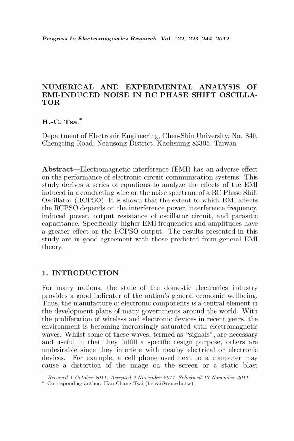
Tt0
Vi(t)
t
V0
Figure 6. Input signal offerromagnetic toroid.
i C
L R
Figure 7. Equivalent circuit offerromagnetic toroid.
and
Kn =V0t0T
sin 12nωt0
12nωt0
(12)
∠Cn =12nωt0 (13)
Substituting Eqs. (12) and (13) into Eq. (9) gives
V (t) =V0
2+
∞∑
n=1
Kn cos(nωt0 +
nπ
2
), for t0 =
T
2(14)
Figure 7 shows the equivalent circuit of the ferromagnetic toroid.The following admittance can be obtained:
Y =(Rω + jnωL) + 1
jnωCω
(Rω+jnωL) 1jnωCω
=1
R2ω+n2ω2L2
[Rω+j
(nωR2
ωCω−nωL+n3ω3L2Cω
)]=|Y |∠θ1 (15)
I (jnω)=Y V (t)=C0Y0+∞∑
n=1
2Kn |Y | cos (nωt+∠Cn+θ1) (16)
From Eq. (7), it can be shown that
Veff = − 1dt
∫
s
~B · d~s = − 1dt
[µ0µNI (jnω)
µ0 (2πr0 − lg) + µlg·∆zd
](17)
=µ0µN (∆zd)
µ0 (2πr0−lg)+µlg
∞∑
n=1
2Kn |Y |nω sin (nωt+∠Cn+θ1) (18)
=∞∑
n=1
2KKn |Y |nω sin (nωt + ∠Cn + θ1)

232 Tsai
K =µ0µN∆zd
µ0 (2πr0 − lg) + µlg(19)
Figure 8 shows the equivalent circuit of the experimentalmeasurement system.
In Fig. 8, the Vout signal supplied to the oscilloscope and signalanalyzer is given by
Vout = VeffK1
RS· K3∠θ3
K2∠θ2· Ri
K4∠θ4(20)
where K1 = RS//Rm Rm = 1/hoe//γL for a small value of Cce.
Q2 = K1 − j1
ωC= K2∠θ2 (21)
K2 =
[K2
1 +(
1ωC
)2] 1
2
θ2 = tan−1 − 1ωC
K1(22)
Q3 = K2∠θ2//RL = K3∠θ3 = a + bj (23)
K3 =1
(K1 + R2)2 +
(1
ωC
)2
[K1RL (K1 + RL) +
R2
ω2C2
]2
+[K1RL
ωC− (K1 + RL)
RL
ωC
]21/2
θ3 = tan−1K1RL
ωC − (K1 + RL) RLωC
K1RL (K1 + RL) + RLω2C2
(24)
Q4 = (Rm//RS + XC) //RL + XC + Ri = Q3 + XC + Ri
= a + Ri + j
(b− 1
ωC
)= K4∠θ4 (25)
C C RS
Signal
Analyzer
Cce Rm RL
Veff
Figure 8. Equivalent circuit of experimental measurement system.
Progress In Electromagnetics Research, Vol. 122, 2012 233
K4 =
[(a + Ri)
2 +(
b− 1ωC
)2] 1
2
(26)
θ4 = tan−1 b− 1ωC
a + Ri(27)
From the preceding equations, it can be shown that
Vout=∞∑
n=1
2KKn |Y |nωK1K3Ri sin(nωt + ∠Cn + θ1 + θ3 − θ2 − θ4)RsK2K4
Vout=∞∑
n=1
C32KKn |Y |nωK1K3Ri
RsK2K4sin(nωt+∠Cn+θ1+θ3−θ2−θ4)(28)
where the constant C3 is the effective inducted coefficient. Equa-tion (28) shows that the magnitude of the EMI-induced noise is gov-erned by the pulse height, the output load, the parasitic capacitance,the interference frequency and the interference amplitude.
3.3. Noise Analysis
Conducting wires (CWs) render IC circuits highly susceptible to theeffects of EMI and noise [17–24]. When a periodic square wave isapplied across points A and B in Fig. 1, the CW in the air gap of theferromagnetic torroid induces a pulse voltage in the RCPSO, whichin turn produces a response noise spectrum. Fig. 9 shows the typicalresponse wave for a periodic pulse with a period T . The periodic pulsefunction can be analyzed by taking the discrete Fourier transformationof function Sn, i.e.,
Sn =1T
0∫
−T0
−A1e−a(T0+t)e−jωntdt +
T0∫
0
A2e−ate−jωntdt
=1T
a− jωn
a2 + ω2n2[E − jD] (29)
where
E = A1e−aT0 + A2 −A2e
−aT0 cosωnT0 −A1 cosωnT0 (30)
D = −A2e−aT0 sinωnT0 + A1 sinωnT0 (31)
S2n =
1T 2(a2 + ω2n2)
[E2 + D2
](32)
in which n is an integer, ω = 2πf = 2π/T , a is the attenuation factorof the exponential function, and A1 and A2 are the amplitudes of the

234 Tsai
0.000 0.001 0.002
-600.0m
-400.0m
-200.0m
0.0
200.0m
400.0m
600.0m
Vo
lta
ge
(V
)
Time (Second)
Measurement
Simulation
Figure 9. Typical response wave of EMI noise induced in RCPSO.
s
eff
R
V Cce Ro= Rs// L
γ //RL//Ri
Figure 10. Simplified representation of EMI output port in Fig. 8.
upper-half and lower-half periods of the EMI induced by the CW,respectively.
The amplitude spectrum of the EMI current can be obtained byplotting Sn against discrete frequencies, i.e., ωn. The square of Sn hasdimensions A2 and corresponds to the current power spectrum Siλ(fn)over 2T [25].
Regarding the parasitic capacitance of the RCPSO, the Nortonequivalent output circuit is shown in Fig. 10. Let VCce = VC andCce = C. It therefore follows that
in = iC + i0 = Cd∆VC
dt+
∆VC
R0⇒ d∆VC
dt+
∆VC
R0C=
inC
(33)
where R0 = Rs//γL//RL//Ri and ∆Vc is the variation of the voltageacross the capacitor.
Progress In Electromagnetics Research, Vol. 122, 2012 235
Taking the Fourier series expansions of ∆Vc and iλ gives
inC
=1C
∞∑n=−∞
αn exp(jωnt) (34)
d(∆Vcn)dt
+∆Vcn
R0C=
1C
αn exp(jωnt) (35)
It can therefore be shown that
∆Vcn = βn exp(jωnt) (36)
whereβn =
αnR0
1 + jωnR0C(37)
Therefore, the noise power spectrum S∆V c(fn) of the RCPSO isgiven by
S∆V c(fn) = 2Tβnβ∗n (38)
S∆V c(fn) = Siλ(fn)R2
0
1 + (ω1nR0C)2(39)
whereSiλ(fn) = 2Tαnα∗n = 2TS2
n (40)
0 2000 4000 6000 8000 10000
-80
-60
-40
-20
0
20
40
SV
c
(fn )
(DB
mA
/Hz^1
/2)
Frequency (Hz)
B:Mea sure me nt
C:Simulation
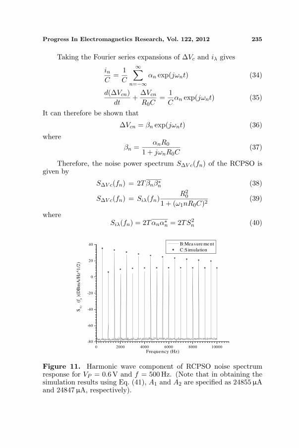
Figure 11. Harmonic wave component of RCPSO noise spectrumresponse for VP = 0.6V and f = 500 Hz. (Note that in obtaining thesimulation results using Eq. (41), A1 and A2 are specified as 24855µAand 24847µA, respectively).

236 Tsai
From Eqs. (32), (39) and (40), it can be shown that
S∆VC(fn) = 2T
R20
1 + (ω1nR0C)2
[1
T 2(a2 + ω2n2)(E2 + D2)
](41)
The total noise power induced in the RCPSO can be obtainedby summing S∆V c(fn) over all possible integers, n. In identifyingthe relative magnitudes of the various harmonic components withinthe power spectrum, the present analysis first finds the value of A(the pulse height) from the measured power spectral intensity ofthe fundamental harmonic and then evaluates the power spectralintensities of the higher-order harmonics. Adopting this approach, thetypical experimental response wave shown in Fig. 9 can be transformedinto the noise spectrum shown in Fig. 11 and the value of the EMI thenquantified directly.
3.4. Effects of Basic Output Frequency of RCPSO onOutput Power
The basic output frequency of a RCPSO has the form of a sinewave. Generally speaking, the effects of the basic output frequencyon the noise power spectrum of an oscillator can be mitigatedusing an impedance-matching method. Fig. 12(a) shows the outputequivalent circuit of the EMI signal supplied to the oscilloscope andsignal analyzer, where RO1 = 1/hoe//RC//RL1//RL//Ri = 41.60Ω.Meanwhile, Fig. 12(b) shows the equivalent circuit of the RCPSOsine wave output signal, where RO2 = 1/hoe//RS//RL1//RL//Ri =23.23Ω. The output powers of the EMI and oscillator signals can be
RC2
RO2 VRC
RS
RO1 Veff
(a) (b)
Figure 12. Output equivalent circuits of (a) EMI signal and (b)RCPSO signal.

Progress In Electromagnetics Research, Vol. 122, 2012 237
obtained respectively as
PEMI =(
Veff
50 + 41.60
)2
41.60 = 0.00496(Veff )2 (42)
PRC =(
VRC
1k + 23.23
)2
23.23 = 2.219× 10⁻⁵(VRC)2 (43)
From Eqs. (42) and (43), PRC/PEMI = 0.00447. In other words, theoutput power of the RCPSO is negligible compared to that of the EMI-induced signal and can therefore be neglected.
4. RESULTS AND DISCUSSION
Figure 9 presents the experimental and simulation results for thetypical periodic pulse function generated in the RCPSO by a periodicEMI signal with a period T . Note that in obtaining the simulationresults using Eq. (28), the following parameter values are assumed:V0 = 0.58 V (at time t = 0), V0 = 0.48V (at time t = T/2),µ0=4πE − 7H/m, µr = 4000, N = 500, F = 500Hz, Rω = 0.52Ω,r0 = 0.09 m, lg = 0.005m, Cω = 6.558E − 10F , 1/hoe = 30 kΩ,RC = 1 kΩ, R1 = R2 = R3 = 1 kΩ, C = 100E − 6F , ∆z = 0.01m,d = 0.001 m, Rs = 50 Ω, C3 = 0.083, XC = 1/(2πfC), RL = 220 kΩ,L = 1E − 4H, ω = 2πf and Ri = 50 Ω. Figure 9 confirms that agood agreement exists between the simulated pulse function and the
0 2000 4000 6000 8000 100000
10
20
30
40
50
SVc
(fn)(
DB
mA
/Hz^1
/2)
Frequency(Hz)
All f=500Hz
1.Vp=1.0V Measurement
S imula tion
2.Vp=0.9V Measurement
S imula tion
3.Vp=0.8V Measurement
S imula tion
4.Vp=0.7V Measurement
S imula tion
5.Vp=0.6V Measurement
S imula tion
6.Vp=0.5V Measurement
S imula tion
7.Vp=0.4V Measurement
S imula tion
8.Vp=0.3V Measurement
S imula tion
Figure 13. Experimental and simulation results for odd-orderharmonics of noise spectrum induced in RCPSO by EMI interferencewith frequency of 500 Hz and amplitude of Vp = 0.3 ∼ 1.0V. (Notethat the simulation results computed using Eq. (41) are shown usingfilled symbols).

238 Tsai
experimental function. In the experimental setup shown in Fig. 1,Cce = 12.77E − 8F , RL = 220 kΩ, and T0 = 0.4942T . Utilizing avalue of a = 10622 in Eq. (41), Fig. 11 compares the experimentaland simulation results for the harmonic wave component of the noisespectrum induced in the RCPSO by EMI with an amplitude ofVP = 0.6V and a frequency of f = 500 Hz. Again, a good agreementis observed between the two sets of results. To further investigatethe effect of EMI on the noise spectrum induced in the RCPSO, theamplitude of the AC interference signal was varied between 0.3 V and1.0V while the frequency was maintained at a constant f = 500Hz.Fig. 13 presents the experimental and simulation results for the odd-order harmonics of the resulting noise spectrum. Note that in obtainingthe simulation results using Eq. (41), A1 ranges from 11057 ∼ 41856µAwhile A2 ranges from 11047 ∼ 41845µA. It is observed that a goodagreement is obtained between the experimental and simulation resultsfor all values of Vp.
Table 1 compares the measured and simulated peak values of theharmonic components of the maximum noise power spectral intensityfor EMI with amplitudes in the range of VP = 0.3 ∼ 1.0V and aconstant frequency of f = 500 Hz. (In other words, the harmonicvalue varies only as a function of the interference amplitude whilethe remaining parameters are constant.) Table 2 compares theexperimental and simulation results for the maximum noise powerspectral intensity for EMI frequencies in the range of 300 Hz ∼ 1 kHzand constant interference amplitudes of A1 = 21455µA and A2 =21447µA. (In other words, the noise power spectral intensity variesonly as a function of the AC interference frequency while the otherparameters remain constant). Fig. 14 presents the experimental andsimulation results for the odd-order harmonics of the noise spectrum
Table 1. Comparison of experimental and theoretical results formaximum noise power spectral intensity of RCPSO for various valuesof Vp.
Frequency fixed, Amplitude variable (First harmonic wave)Vp (V) 0.3 0.4 0.5 0.6 0.7 0.8 0.9 1.0
Frequency (Hz) 500 500 500 500 500 500 500 500Measurement
(dBmA/Hz1/2)28.4 31.1 33.3 35.3 36.8 37.6 38.8 39.9
Simulation(dBmA/Hz1/2)
28.6 31.5 33.4 35.4 36.8 37.8 38.9 39.9

Progress In Electromagnetics Research, Vol. 122, 2012 239
Table 2. Comparison of experimental and theoretical results formaximum noise power spectral intensity of RCPSO for various valuesof frequency.
Amplitude fixed, Frequency variable (First harmonic wave)Frequency (Hz) 300 400 500 600 700 800 900 1000Measurement
(dBmA/Hz1/2)31.2 32.7 34 34.6 35.6 35.9 36.3 36.6
Simulation(dBmA/Hz1/2)
32.2 33.3 34.2 34.8 35.3 35.7 36 36.3
0 1000 2000 3000 4000 5000 6000 7000 8000 9000 100000
10
20
30
40
SVc
(fn )
(DB
mA
/Hz^1
/2)
Frequency(Hz)
All Vp=0.5V
1.F=700Hz Me as urement
Simula tion
2.F=600Hz Me as urement
Simula tion
3.F=500Hz Me as urement
Simula tion
4.F=400Hz Me as urement
Simula tion
5.F=300Hz Me as urement
Simula tion
Figure 14. Experimental and simulation results for odd-orderharmonics of noise spectrum induced in RCPSO by EMI interferencefrequency of 300 ∼ 700 Hz and amplitude of Vp = 0.5 V. (Note thatthe simulation results computed using Eq. (41) are shown using filledsymbols).
induced in the RCPSO by EMI interference with a frequency of300 ∼ 700Hz and an amplitude of Vp = 0.5V. Although a −2 dBdifference is observed between the two sets of results, it is clear thatthe EMI frequency has a significant effect on the noise response ofthe RCPSO. By tuning the amplitude parameters in recognition of thefact that a variable EMI frequency affects both the attenuation factorand the induced wave type, the same degree of simulation accuracy asthat shown in Fig. 13 can be obtained (see Fig. 15 and Table 3). Inother words, the EMI frequency is a function of the EMI amplitude,as proven in Eqs. (28) and (41).
Although Fig. 14 shows that the frequency has a significant effect

240 Tsai
0 1000 2000 3000 4000 5000 6000 7000 8000 9000 100000
10
20
30
40
SV
c
(fn )
(DB
mA
/Hz
^1/2
)
Frequency(Hz)
All Vp=0.5V
1.F=700Hz Me asurement
S imula tion
2.F=600Hz Me asurement
S imula tion
3.F=500Hz Me asurement
S imula tion
4.F=400Hz Me asurement
S imula tion
5.F=300Hz Me asurement
S imula tion
Figure 15. Experimental and simulation results for odd-orderharmonics of noise spectrum induced in RCPSO by EMI interferencefrequency of 300 ∼ 700Hz and variable amplitude parameters A1 andA2 (see Table 3). (Note that the simulation results computed usingEq. (41) are shown using filled symbols).
Table 3. Comparison of experimental and theoretical results formaximum noise power spectral intensity of RCPSO for various valuesof frequency and amplitude.
Amplitude, Frequency variable (First harmonic wave)Frequency (Hz) 300 400 500 600 700
InducedCurrent A1(µA)
18656 19954 21455 21554 23056
InducedCurrent A2 (µA)
18648 19946 21447 21548 23045
Measurement(dBmA/Hz1/2)
31.2 32.7 34 34.6 35.6
Simulation(dBmA/Hz1/2)
30.9 32.7 34.1 34.8 35.9
on the odd-order harmonic waves (i.e., Eq. (41) denotes dω/dA1 6= 0and dω/dA2 6= 0 for the nonlinear function S∆V c(fn)), Fig. 13 showsthat the difference between the experimental and simulation results forthe variable amplitude case is less than that for the variable frequencycase. In other words, the amplitude of the EMI has a greater effect onthe noise response of the RCPSO than the frequency. In practice, thisimplies that the parasitic capacitance and dynamic input resistance of
Progress In Electromagnetics Research, Vol. 122, 2012 241
Table 4. Relative SNR of current induced by EMI.
VP (V) 1.0 0.9 0.8 0.7 0.6 0.5 0.4 0.3InducedCurrentA1 (µA)
41856 37354 32855 29356 24855 19654 15653 11057
InducedCurrentA2(µA)
41845 37346 32848 29348 24847 19646 15648 11047
InducedPeak
CurrentNi (µA)
8.37 7.47 6.57 5.87 4.97 3.93 3.13 2.21
RelativeSNR (dBµA)
1.545∗ 2.534∗ 3.649∗ 4.627∗ 6.073∗ 8.112∗ 10.089∗13.112∗
*Where SNR = 20 log(Si/Ni), Si = 10 µA, Ni = ((A1 + A2)/2)/5000and f = 500Hz.
the RCPSO vary with a varying frequency.In general, the simulation and experimental results presented
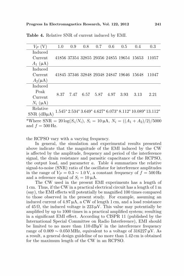
above indicate that the magnitude of the EMI induced by the CWis affected by the amplitude, frequency and period of the interferencesignal, the drain resistance and parasitic capacitance of the RCPSO,the output load, and parameter a. Table 4 summarizes the relativesignal-to-noise (SNR) ratio of the oscillator for interference amplitudesin the range of VP = 0.3 ∼ 1.0 V, a constant frequency of f = 500 Hzand a reference signal of Si = 10µA.
The CW used in the present EMI experiments has a length of1 cm. Thus, if the CW in a practical electrical circuit has a length of 1m(say), the EMI effects will potentially be magnified 100 times comparedto those observed in the present study. For example, assuming aninduced current of 4.97µA, a CW of length 1 cm, and a load resistanceof 45 Ω, the induced voltage is 223µV. This value may potentially beamplified by up to 1000 times in a practical amplified system; resultingin a significant EMI effect. According to CISPR 11 (published by theInternational Special Committee on Radio Interference), EMI shouldbe limited to no more than 110 dBµV in the interference frequencyrange of 0.009 ∼ 0.050MHz, equivalent to a voltage of 316227µV. Asa result, a general design guideline of no more than 1.42 cm is obtainedfor the maximum length of the CW in an RCPSO.

242 Tsai
5. CONCLUSION
Experimental and theoretical methods have been used to characterizethe noise spectrum of an RCPSO subject to periodic EMI induced viaa CW. A good agreement has been observed between the experimentaland simulation results for the noise spectral intensity of the RCPSO inboth the time domain and the frequency domain. In general, the resultshave shown that the noise response of the oscillator is significantlyaffected by EMI. Specifically, the degree of the EMI effect on theRCPSO is determined by the radiated power of the interference sourceand the following circuit parameters: f , V0, µ0, µr, N , Rω, r0, lg,Rs, RC , R1, R2, R3, Cω, Cce, Ri, ∆z, d, L, A1, A2, a, T0, RL andC. Furthermore, it has been shown that the magnitude of the inducedinterference current increases with an increasing interference frequencyand an increasing interference amplitude. Of these two factors, theamplitude of the EMI has a greater effect on the noise response ofthe oscillator than the frequency. In accordance with CISPR and ENnorms, the results presented in this study suggest that the length of theCWs used in practical RCPSOs should not exceed 1.42 cm. Whilst themethods outlined in this study have focused specifically on the case ofRCPSOs, they are equally applicable to the EMI analysis of all generalwavelength-based electronic devices.
ACKNOWLEDGMENT
The author wishes to acknowledge the invaluable assistance providedby Tsair-Jan Hwang in the course of this study.
REFERENCES
1. Hung, F. S., F. Y. Hung, and C. M. Chiang, “Crystallization andannealing effects of sputtered tin alloy films on electromagneticinterference shielding,” Applied Surface Science, Vol. 257, 3733–3738, 2011.
2. Hu, C. N. and H. C. Ko, “Improved IC production yield by takinginto account the electromagnetic interference level during testing,”IEEE Transactions on Electromagnetic Compatibility, Vol. 53,No. 2, 266–273, 2011.
3. Mustafa, F. and A. M. Hashim, “Properties of electromagneticfields and effective permittivity excited by drifting plasma wavesin semiconductor-insulator interface structure and equivalenttransmission line technique for multi-layered structure,” ProgressIn Electromagnetics Research, Vol. 104, 403–425, 2010.

Progress In Electromagnetics Research, Vol. 122, 2012 243
4. Mustafa, F. and A. M. Hashim, “Generalized 3D transverse mag-netic mode method for analysis of interaction between driftingplasma waves in 2 deg-structured semiconductors and electromag-netic space harmonic waves,” Progress In Electromagnetics Re-search, Vol. 102, 315–335, 2010.
5. Tsai, H.-C., “Investigation into time- and frequency-domainEMI-induced noise in bistable multivibrator,” Progress InElectromagnetics Research, Vol. 100, 327–349, 2010.
6. Yang, T., Y. Bayram, and J. L. Volakis, “Hybrid analysis ofelectromagnetic interference effects on microwave active circuitswithin cavity enclosures,” IEEE Transactions on ElectromagneticCompatibility, Vol. 52, No. 3, 745–748, 2010.
7. Khah, S. K., T. Chakravarty, and P. Balamurali, “Analysis ofan electromagnetically coupled microstrip ring antenna usingan extended feedline,” Journal of Electromagnetic Waves andApplications, Vol. 23, No. 2–3, 369–376, 2009.
8. Hong, J.-I., S.-M. Hwang, and C.-S. Huh, “Susceptibility ofmicrocontroller devices due to coupling effects under narrow-band high power electromagnetic waves by magnetron,” Journalof Electromagnetic Waves and Applications, Vol. 22, No. 17–18,2451–2462, 2009.
9. Dlugosz, T. and H. Trzaska, “A new calibration method fornon-stationary electromagnetic fields measurements,” Journal ofElectromagnetic Waves and Applications, Vol. 23, No. 17–18,2471–2480, 2009.
10. Heydari, H., V. Abbasi, and F. Faghihi, “Impact of switching-induced electromagnetic interference on low-voltage cables in sub-stations,” IEEE Transactions on Electromagnetic Compatibility,Vol. 51, No. 4, 937–944, 2009.
11. Toh, T. C., “Electromagnetic interference laboratory correlationstudy and margin determination,” IEEE Transactions onElectromagnetic Compatibility, Vol. 51, No. 2, 204–209, 2009.
12. Tsai, H. C. and K. C. Wang, “Investigation of EMI-inducednoise spectrum on an enhancement-type MOSFET,” Solid StateElectronics, Vol. 52, No. 8, 1207–1216, 2008.
13. Kim, Y. J., U. Choi, and Y. S. Kim, “Screen filter designconsiderations for plasma display panels (PDP) to achieve a highbrightness with a minimal loss of EMI shielding effectiveness,”Journal of Electromagnetic Waves and Applications, Vol. 22,No. 5–6, 775–786, 2008.
14. Tsai, H. C., “Numerical and experimental analysis of EMI effectson circuits with MESFET devices,” Microelectronics Reliability,

244 Tsai
Vol. 48, No. 4, 537–546, 2008.15. Tsai, H. C., “An investigation on the influence of electromagnetic
interference induced in conducting wire of universal LEDs,”Microelectronics Reliability, Vol. 47, No. 6, 959–966, 2007.
16. Cheng, D. K., Field and Wave Electromagnetics, 2nd Edition,252–634, Addison-Wesley Publishing Company, USA, 1989.
17. Yan, L., F.-L. Yang, and C.-L. Fu, “A new numerical methodfor the inverse source problem from a Bayesian perspective,”International Journal for Numerical Methods in Engineering,Vol. 85, No. 11, 1460–1474, 2011.
18. Lee, H. S., Y. H. Hong, and H. W. Park, “Design of an FIR filterfor the displacement reconstruction using measured accelerationin low-frequency dominant structures,” International Journal forNumerical Methods in Engineering, Vol. 82, No. 4, 403–434, 2010.
19. Tsai, H.-C. and K.-C. Wang, “Simulated and experimentalanalysis of surface state and 1/f r noise on GaAs MESFETdevices,” Japanese Journal of Applied Physics, Vol. 48, No. 7,071101-1–8, 2009.
20. Bhatia, V. and B. Mulgrew, “Non-parametric likelihood basedchannel estimator for Gaussian mixture noise,” Signal Processing,Vol. 87, No. 11, 2569–2586, 2007.
21. Chambers, J., D. Bullock, Y. Kahana, A. Kots, and A. Palmer,“Developments in active noise control sound systems for magneticresonance imaging,” Applied Acoustics, Vol. 68, No. 3, 281–295,2007.
22. Roelant, R., D. Constales, G. S. Yablonsky, R. van Keer,M. A. Rude, and G. B. Marin, “Noise in temporal analysisof products (TAP) pulse responses,” Catalysis Today, Vol. 121,No. 3–4, 269–281, 2007.
23. Lisnanski, R. and J. A. Weiss, “Low complexity generalizedEM algorithm for blind channel estimation and data detectionin optical communication systems,” Signal Processing, Vol. 86,No. 11, 3393–3403, 2006.
24. Li, H. G. and G. Meng, “Detection of harmonic signals fromchaotic interference by empirical mode decomposition,” Chaos,Solitons and Fractals, Vol. 30, No. 4, 930–935, 2006.
25. Van der Ziel, A., Noise in Solid State Devices and Circuits, 10–20,Wiley, New York, 1986.