numicro family m051 dn/de series product briefdn_de)_series_en... · 2015-10-20 · numicro®...
TRANSCRIPT

M051 DN/DE
Oct. 05, 2015 Page 1 of 19 Rev 1.02
M051
DN
/DE
SE
RIE
S P
RO
DU
CT
BR
IEF
ARM® Cortex
®-M0
32-bit Microcontroller
NuMicro® Family
M051 DN/DE Series
Product Brief
The information described in this document is the exclusive intellectual property of Nuvoton Technology Corporation and shall not be reproduced without permission from Nuvoton.
Nuvoton is providing this document only for reference purposes of NuMicro microcontroller based system design. Nuvoton assumes no responsibility for errors or omissions.
All data and specifications are subject to change without notice.
For additional information or questions, please contact: Nuvoton Technology Corporation.
www.nuvoton.com
M051 DN/DE
Oct. 05, 2015 Page 2 of 19 Rev 1.02
M051
DN
/DE
SE
RIE
S P
RO
DU
CT
BR
IEF
Table of Contents
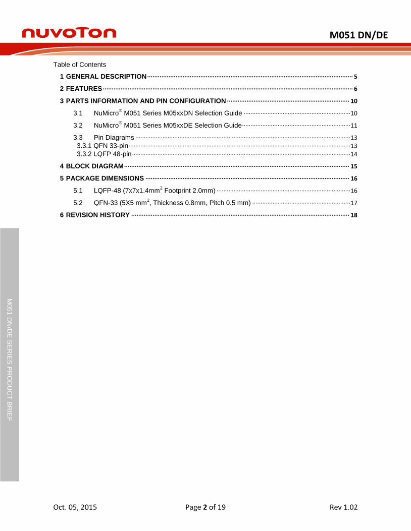
1 GENERAL DESCRIPTION ···················································································································· 5
2 FEATURES ············································································································································· 6
3 PARTS INFORMATION AND PIN CONFIGURATION ····································································· 10
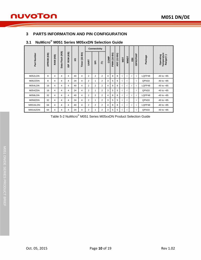
NuMicro® M051 Series M05xxDN Selection Guide ······························································· 10 3.1
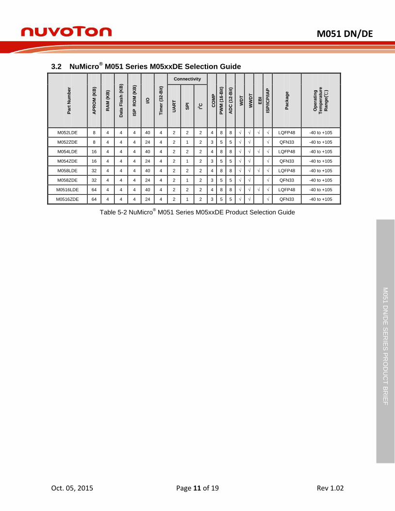
NuMicro® M051 Series M05xxDE Selection Guide ································································ 11 3.2
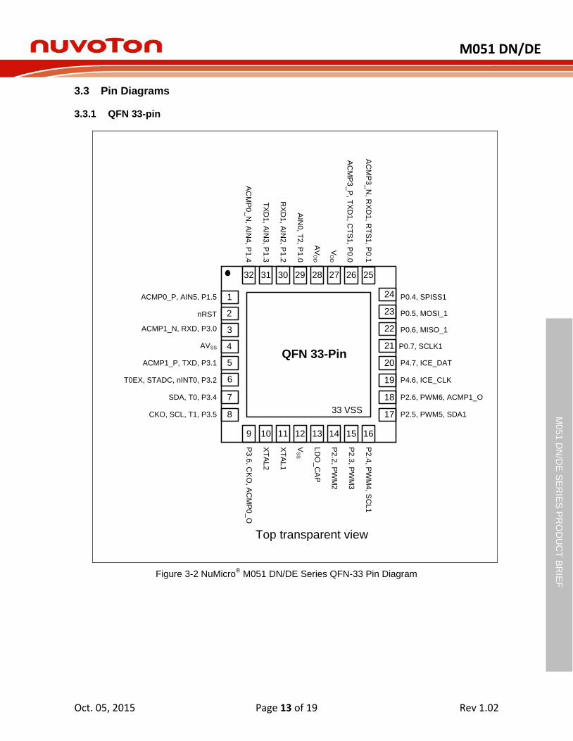
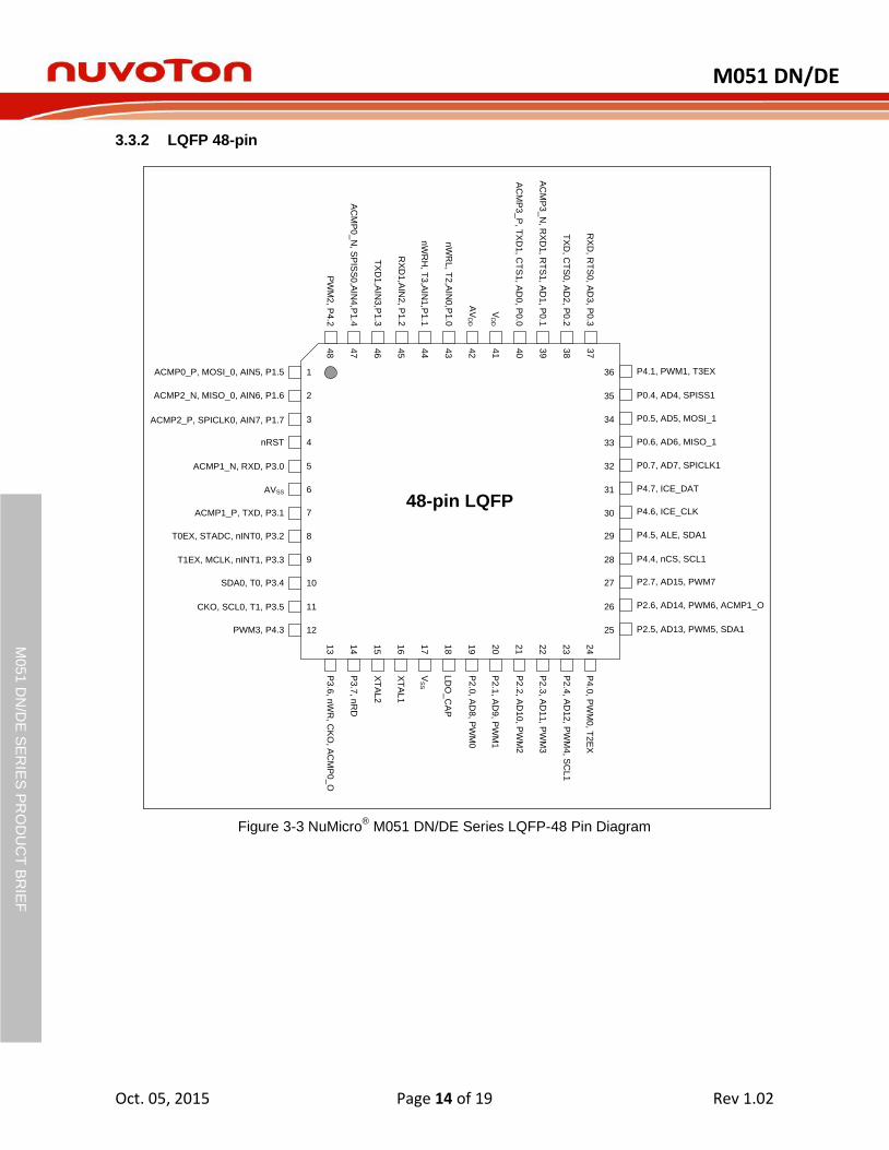
Pin Diagrams ······························································································································· 13 3.3
3.3.1 QFN 33-pin ··································································································································· 13 3.3.2 LQFP 48-pin ································································································································· 14
4 BLOCK DIAGRAM ······························································································································· 15
5 PACKAGE DIMENSIONS ··················································································································· 16
LQFP-48 (7x7x1.4mm2 Footprint 2.0mm) ··············································································· 16 5.1
QFN-33 (5X5 mm2, Thickness 0.8mm, Pitch 0.5 mm) ·························································· 17 5.2
6 REVISION HISTORY ··························································································································· 18
M051 DN/DE
Oct. 05, 2015 Page 3 of 19 Rev 1.02
M051
DN
/DE
SE
RIE
S P
RO
DU
CT
BR
IEF
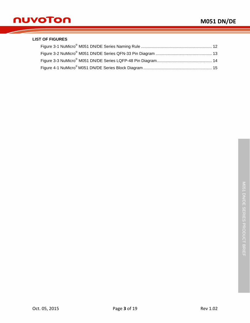
LIST OF FIGURES
Figure 3-1 NuMicro® M051 DN/DE Series Naming Rule ............................................................... 12
Figure 3-2 NuMicro® M051 DN/DE Series QFN-33 Pin Diagram .................................................. 13
Figure 3-3 NuMicro® M051 DN/DE Series LQFP-48 Pin Diagram................................................. 14
Figure 4-1 NuMicro®
M051 DN/DE Series Block Diagram ............................................................. 15

M051 DN/DE
Oct. 05, 2015 Page 4 of 19 Rev 1.02
M051
DN
/DE
SE
RIE
S P
RO
DU
CT
BR
IEF
LIST OF TABLES
Table 1-1 M05xxBN, M05xxDN and M05xxDE Difference List ........................................................ 5

M051 DN/DE
Oct. 05, 2015 Page 5 of 19 Rev 1.02
M051
DN
/DE
SE
RIE
S P
RO
DU
CT
BR
IEF
1 GENERAL DESCRIPTION
The NuMicro® M051 DN/DE series 32-bit microcontroller is embedded with ARM
® Cortex
®-M0
core for industrial control and applications which need rich communication interfaces. The NuMicro
® M051 DN/DE series includes the following part numbers: M052xDN/xDE,
M054xDN/xDE, M058xDN/xDE and M0516xDN/xDE.
The NuMicro® M051 DN/DE series can run up to 50 MHz and operate at 2.5V ~ 5.5V, -40℃ ~
85℃, while M05xxDE operates at -40℃ ~ 105℃, and thus can afford to support a variety of
industrial control and applications which need high CPU performance. The NuMicro® M051
DN/DE series offers 8/16/32/64 KB flash, 4 KB Data Flash, 4 KB flash for the ISP, and 4 KB SRAM.
Many system level peripheral functions, such as I/O Port, EBI (External Bus Interface), Timer, UART, SPI, I
2C, PWM, ADC, Watchdog Timer, Window Watchdog Timer, Analog Comparator and
Brown-out Detector, have been incorporated into The NuMicro® M051 DN/DE series in order to
reduce component count, board space and system cost. These useful functions make The NuMicro
® M051 DN/DE series powerful for a wide range of applications.
Additionally, the NuMicro® M051 DN/DE series is equipped with ISP (In-System Programming)
and ICP (In-Circuit Programming) functions, and IAP (In-Application Programming), which allow the user to update the program memory without removing the chip from the actual end product.
Item M05xxBN M05xxDN M05xxDE
Operating Temperature -40℃ ~ 85℃ -40℃ ~ 85℃ -40℃ ~ 105℃
Hardware Divider - ● ●
IAP Mode - ● ●
Window WDT - ● ●
Analog Comparators 2 4 4
Configurable I/O mode after POR
- ● ●
I2C 1
2 (Supports Wake-up)
2 (Supports Wake-up)
SPI
- Only Supports HCLK as SPI clock source
- No FIFO
- Supports HCLK and PLL as SPI clock source
- 4-level FIFO
- Supports HCLK and PLL as SPI clock source
- 4-level FIFO
PWM and ADC PWM cannot trigger ADC - PWM can trigger ADC conversion
- PWM can trigger ADC conversion
Table 1-1 M05xxBN, M05xxDN and M05xxDE Difference List
M051 DN/DE
Oct. 05, 2015 Page 6 of 19 Rev 1.02
M051
DN
/DE
SE
RIE
S P
RO
DU
CT
BR
IEF
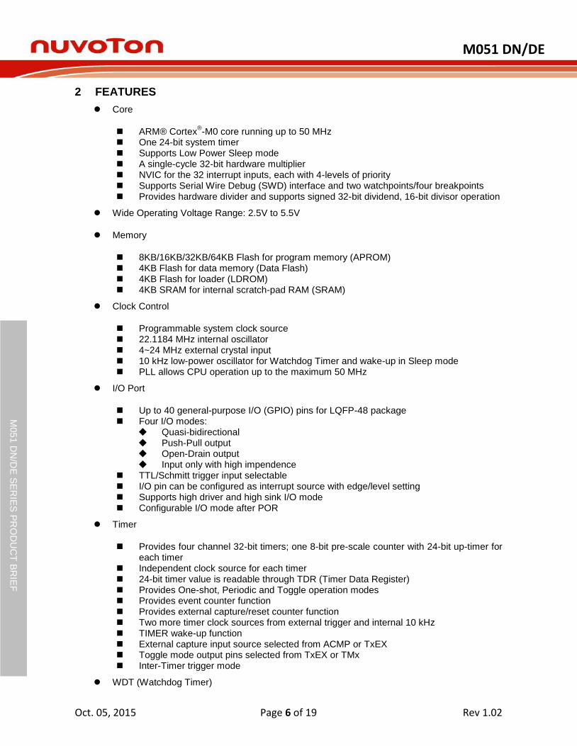
2 FEATURES
Core
ARM® Cortex®-M0 core running up to 50 MHz
One 24-bit system timer Supports Low Power Sleep mode A single-cycle 32-bit hardware multiplier NVIC for the 32 interrupt inputs, each with 4-levels of priority Supports Serial Wire Debug (SWD) interface and two watchpoints/four breakpoints Provides hardware divider and supports signed 32-bit dividend, 16-bit divisor operation
Wide Operating Voltage Range: 2.5V to 5.5V
Memory
8KB/16KB/32KB/64KB Flash for program memory (APROM) 4KB Flash for data memory (Data Flash) 4KB Flash for loader (LDROM) 4KB SRAM for internal scratch-pad RAM (SRAM)
Clock Control
Programmable system clock source 22.1184 MHz internal oscillator 4~24 MHz external crystal input 10 kHz low-power oscillator for Watchdog Timer and wake-up in Sleep mode PLL allows CPU operation up to the maximum 50 MHz
I/O Port
Up to 40 general-purpose I/O (GPIO) pins for LQFP-48 package Four I/O modes:
Quasi-bidirectional Push-Pull output Open-Drain output Input only with high impendence
TTL/Schmitt trigger input selectable I/O pin can be configured as interrupt source with edge/level setting Supports high driver and high sink I/O mode Configurable I/O mode after POR
Timer
Provides four channel 32-bit timers; one 8-bit pre-scale counter with 24-bit up-timer for each timer
Independent clock source for each timer 24-bit timer value is readable through TDR (Timer Data Register) Provides One-shot, Periodic and Toggle operation modes Provides event counter function Provides external capture/reset counter function Two more timer clock sources from external trigger and internal 10 kHz TIMER wake-up function External capture input source selected from ACMP or TxEX Toggle mode output pins selected from TxEX or TMx Inter-Timer trigger mode
WDT (Watchdog Timer)

M051 DN/DE
Oct. 05, 2015 Page 7 of 19 Rev 1.02
M051
DN
/DE
SE
RIE
S P
RO
DU
CT
BR
IEF
Multiple clock sources Supports wake-up from Power-down or Sleep mode Interrupt or reset selectable on watchdog time-out Time-out reset delay period time can be selected
WWDT (Window Watchdog Timer)
6-bit down counter with 11-bit pre-scale for wide range window selected
PWM
Up to four built-in 16-bit PWM generators, providing eight PWM outputs or four complementary paired PWM outputs
Individual clock source, clock divider, 8-bit pre-scalar and dead-zone generator for each PWM generator
PWM interrupt synchronized to PWM period 16-bit digital Capture timers with rising/falling capture inputs Supports capture interrupt Internal 10 kHz to PWM clock source Polar inverse function Center-aligned type function Timer duty interrupt enable function Two kinds of PWM interrupt period/duty type selection Period/duty trigger ADC function PWM Timer synchronous start function
UART
Up to two sets of UART devices Programmable baud-rate generator Buffered receiver and transmitter, each with 15 bytes FIFO Optional flow control function (CTS and RTS) Supports IrDA(SIR) function Supports RS485 function Supports LIN function
SPI
Up to two sets of SPI devices Supports Master/Slave mode Full-duplex synchronous serial data transfer Provides 3 wire function Variable length of transfer data from 1 to 32 bits MSB or LSB first data transfer Rx latching data can be either at rising edge or at falling edge of serial clock Tx sending data can be either at rising edge or at falling edge of serial clock Supports Byte Suspend mode in 32-bit transmission PLL clock source 4-level depth FIFO buffer for better performance and flexibility in SPI Burst Transfer
mode

M051 DN/DE
Oct. 05, 2015 Page 8 of 19 Rev 1.02
M051
DN
/DE
SE
RIE
S P
RO
DU
CT
BR
IEF
I2C
Up to two sets of I2C modules
Supports Master/Slave mode Bidirectional data transfer between master and slave Multi-master bus (no central master) Arbitration between simultaneously transmitting masters without corruption of serial
data on the bus Serial clock synchronization allows devices with different bit rates to communicate via
one serial bus Serial clock synchronization can be used as a handshake mechanism to suspend and
resume serial transfer Programmable clocks allow versatile rate control Supports multiple address recognition (four slave addresses with mask option)
ADC
12-bit SAR ADC Up to 8-ch single-ended input or 4-ch differential input Supports Single mode/Burst mode/Single-cycle Scan mode/Continuous Scan mode Supports 2’ complement/un-signed format in differential mode conversion results Each channel with an individual result register Supports conversion value monitoring (or comparison) for threshold voltage detection Conversion started either by software trigger or external pin trigger A/D conversion started by PWM center-aligned trigger or edge-aligned trigger PWM trigger delay function Supports conversion result with signed format in Differential input and Burst mode
Analog Comparator
Up to four sets of Comparator analog modules External input or internal band-gap voltage selectable at negative node Interrupt when compared results change Power-down wake-up
EBI (External Bus Interface) for external memory-mapped device access
Accessible space: 64 KB in 8-bit mode or 128 KB in 16-bit mode Supports 8-bit or 16-bit data width Supports byte-write in 16-bit data width
ISP (In-System Programming) and ICP (In-Circuit Programming)
IAP (In-Application Programming)
One built-in temperature sensor with 1℃ resolution
BOD (Brown-out Detector)
With 4 levels: 4.4V/3.7V/2.7V/2.2V Supports Brown-out interrupt and reset option
96-bit unique ID
LVR (Low Voltage Reset)
Threshold voltage level: 2.0V
Operating Temperature:
M051 DN/DE
Oct. 05, 2015 Page 9 of 19 Rev 1.02
M051
DN
/DE
SE
RIE
S P
RO
DU
CT
BR
IEF
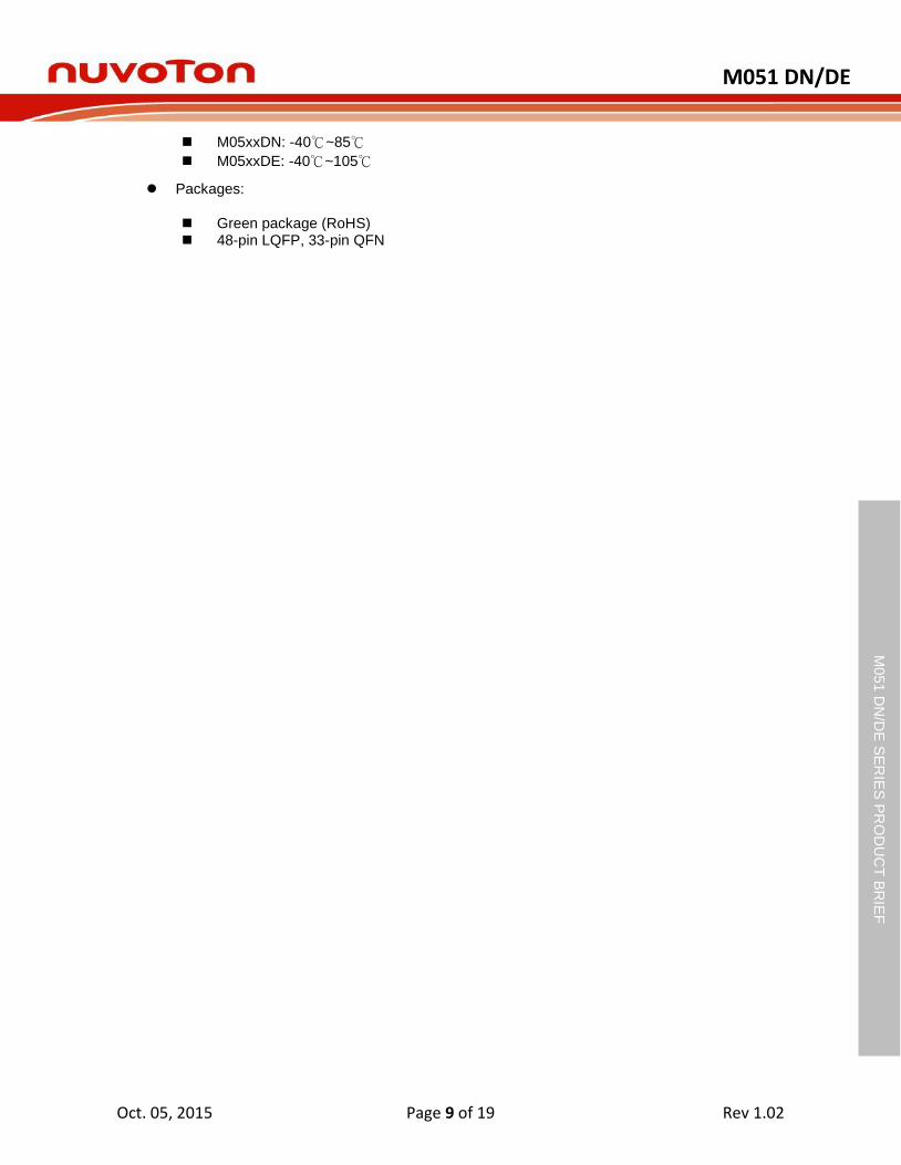
M05xxDN: -40℃~85℃
M05xxDE: -40℃~105℃
Packages:
Green package (RoHS) 48-pin LQFP, 33-pin QFN
M051 DN/DE
Oct. 05, 2015 Page 10 of 19 Rev 1.02
M051
DN
/DE
SE
RIE
S P
RO
DU
CT
BR
IEF
3 PARTS INFORMATION AND PIN CONFIGURATION
NuMicro® M051 Series M05xxDN Selection Guide 3.1
Part
Nu
mb
er
AP
RO
M (
KB
)
RA
M (
KB
)
Data
Fla
sh
(K
B)
ISP
R
OM
(K
B)
I/O
Tim
er
(32
-Bit
)
Connectivity
CO
MP
PW
M (
16
-Bit
)
AD
C (
12-B
it)
WD
T
WW
DT
EB
I
ISP
/IC
P/IA
P
Pack
ag
e
Op
era
tin
g
Tem
pera
ture
Ran
ge
(℃)
UA
RT
SP
I
I2C
M052LDN 8 4 4 4 40 4 2 2 2 4 8 8 √ √ √ √ LQFP48 -40 to +85
M052ZDN 8 4 4 4 24 4 2 1 2 3 5 5 √ √ √ QFN33 -40 to +85
M054LDN 16 4 4 4 40 4 2 2 2 4 8 8 √ √ √ √ LQFP48 -40 to +85
M054ZDN 16 4 4 4 24 4 2 1 2 3 5 5 √ √ √ QFN33 -40 to +85
M058LDN 32 4 4 4 40 4 2 2 2 4 8 8 √ √ √ √ LQFP48 -40 to +85
M058ZDN 32 4 4 4 24 4 2 1 2 3 5 5 √ √ √ QFN33 -40 to +85
M0516LDN 64 4 4 4 40 4 2 2 2 4 8 8 √ √ √ √ LQFP48 -40 to +85
M0516ZDN 64 4 4 4 24 4 2 1 2 3 5 5 √ √ √ QFN33 -40 to +85
Table 5-2 NuMicro® M051 Series M05xxDN Product Selection Guide
M051 DN/DE
Oct. 05, 2015 Page 11 of 19 Rev 1.02
M051
DN
/DE
SE
RIE
S P
RO
DU
CT
BR
IEF
NuMicro® M051 Series M05xxDE Selection Guide 3.2
Part
Nu
mb
er
AP
RO
M (
KB
)
RA
M (
KB
)
Data
Fla
sh
(K
B)
ISP
R
OM
(K
B)
I/O
Tim
er
(32
-Bit
)
Connectivity
CO
MP
PW
M (
16
-Bit
)
AD
C (
12-B
it)
WD
T
WW
DT
EB
I
ISP
/IC
P/IA
P
Pack
ag
e
Op
era
tin
g
Tem
pera
ture
Ran
ge
(℃)
UA
RT
SP
I
I2C
M052LDE 8 4 4 4 40 4 2 2 2 4 8 8 √ √ √ √ LQFP48 -40 to +105
M052ZDE 8 4 4 4 24 4 2 1 2 3 5 5 √ √ √ QFN33 -40 to +105
M054LDE 16 4 4 4 40 4 2 2 2 4 8 8 √ √ √ √ LQFP48 -40 to +105
M054ZDE 16 4 4 4 24 4 2 1 2 3 5 5 √ √ √ QFN33 -40 to +105
M058LDE 32 4 4 4 40 4 2 2 2 4 8 8 √ √ √ √ LQFP48 -40 to +105
M058ZDE 32 4 4 4 24 4 2 1 2 3 5 5 √ √ √ QFN33 -40 to +105
M0516LDE 64 4 4 4 40 4 2 2 2 4 8 8 √ √ √ √ LQFP48 -40 to +105
M0516ZDE 64 4 4 4 24 4 2 1 2 3 5 5 √ √ √ QFN33 -40 to +105
Table 5-2 NuMicro® M051 Series M05xxDE Product Selection Guide

M051 DN/DE
Oct. 05, 2015 Page 12 of 19 Rev 1.02
M051
DN
/DE
SE
RIE
S P
RO
DU
CT
BR
IEF
XM0 5X - X X
ARM Cortex M0
L: LQFP48Z: QFN33
N: - 40℃ ~ +85℃
- X
CPU core
52: 08 KB Flash ROM
54: 16 KB Flash ROM
58: 32 KB Flash ROM516: 64 KB Flash ROM
Reserved
Part Number Temperature
Package
E: - 40℃~ +105℃
Figure 3-1 NuMicro® M051 DN/DE Series Naming Rule
M051 DN/DE
Oct. 05, 2015 Page 13 of 19 Rev 1.02
M051
DN
/DE
SE
RIE
S P
RO
DU
CT
BR
IEF
Pin Diagrams 3.3
3.3.1 QFN 33-pin
ACMP0_P, AIN5, P1.5
AVSS
ACMP1_N, RXD, P3.0
ACMP1_P, TXD, P3.1
SDA, T0, P3.4
CKO, SCL, T1, P3.5
XT
AL
2
XT
AL
1
VS
S
LD
O_C
AP
P2
.2, P
WM
2
P2
.3, P
WM
3
P2
.4, P
WM
4, S
CL
1
P3
.6, C
KO
, AC
MP
0_
O
P0.7, SCLK1
P4.6, ICE_CLK
P0.6, MISO_1
P0.5, MOSI_1
P0.4, SPISS1
P2.5, PWM5, SDA1
P2.6, PWM6, ACMP1_O
P4.7, ICE_DAT
TX
D1, A
IN3
, P1.3
RX
D1, A
IN2
, P1.2
AC
MP
0_N
, AIN
4, P
1.4
AIN
0, T
2, P
1.0
AC
MP
3_P
, TX
D1, C
TS
1, P
0.0
AV
DD
AC
MP
3_N
, RX
D1, R
TS
1, P
0.1
VD
D
33 VSS
32
24
QFN 33-Pin
31 30 29 28 27 26 25
23
22
21
20
19
18
17
109 11 12 13 14 15 16
7
8
Top transparent view
nRST
T0EX, STADC, nINT0, P3.2
1
2
3
4
5
6
Figure 3-2 NuMicro® M051 DN/DE Series QFN-33 Pin Diagram
M051 DN/DE
Oct. 05, 2015 Page 14 of 19 Rev 1.02
M051
DN
/DE
SE
RIE
S P
RO
DU
CT
BR
IEF
3.3.2 LQFP 48-pin
2
44
1
4
3
6
5
8
7
10
9
11
48
42
41
40
39
38
37
32
33
30
31
28
29
26
27
25
13
14
15
16
18
19
20
21
22
12
17
23
24
34
35
36
46
47
43
45
PWM3, P4.3
P4
.0, P
WM
0, T
2E
X
48-pin LQFP
PW
M2, P
4.2
ACMP2_N, MISO_0, AIN6, P1.6
ACMP0_P, MOSI_0, AIN5, P1.5
nRST
ACMP2_P, SPICLK0, AIN7, P1.7
AVSS
ACMP1_N, RXD, P3.0
ACMP1_P, TXD, P3.1
SDA0, T0, P3.4
CKO, SCL0, T1, P3.5
T0EX, STADC, nINT0, P3.2
T1EX, MCLK, nINT1, P3.3
XT
AL
2
XT
AL
1
VS
S
P2
.1, A
D9
, PW
M1
LD
O_
CA
P
P2
.2, A
D1
0, P
WM
2
P2
.3, A
D1
1, P
WM
3
P2
.4, A
D1
2, P
WM
4, S
CL
1
P2
.0, A
D8
, PW
M0
P3
.7, n
RD
P3
.6, n
WR
, CK
O, A
CM
P0
_O
P4.5, ALE, SDA1
P0.7, AD7, SPICLK1
P4.6, ICE_CLK
P0.6, AD6, MISO_1
P0.5, AD5, MOSI_1
P0.4, AD4, SPISS1
P2.5, AD13, PWM5, SDA1
P2.6, AD14, PWM6, ACMP1_O
P2.7, AD15, PWM7
P4.7, ICE_DAT
P4.1, PWM1, T3EX
TX
D1,A
IN3
,P1.3
RX
D1,A
IN2, P
1.2
AC
MP
0_N
, SP
ISS
0,A
IN4
,P1.4
AC
MP
3_
P, T
XD
1, C
TS
1, A
D0, P
0.0
AV
DD
AC
MP
3_N
, RX
D1, R
TS
1, A
D1, P
0.1
TX
D, C
TS
0, A
D2, P
0.2
RX
D, R
TS
0, A
D3, P
0.3
VD
D
P4.4, nCS, SCL1
nW
RH
, T3,A
IN1
,P1.1
nW
RL, T
2,A
IN0
,P1.0
Figure 3-3 NuMicro® M051 DN/DE Series LQFP-48 Pin Diagram

M051 DN/DE
Oct. 05, 2015 Page 15 of 19 Rev 1.02
M051
DN
/DE
SE
RIE
S P
RO
DU
CT
BR
IEF
4 BLOCK DIAGRAM
ARMCortex-M0
50MHz
Memory
APROM64/32/16/8 KB
DataFlash4 KB
SRAM4 KB
PWM / Timer Analog Interface
32-bit Timer x 4
PWM/CaptureTimer x 8
Watchdog Timer 12-bit ADC x 8
Power Control Clock Control
LDO
Power On Reset
LVR
Brownout Detection
High SpeedOscillator
22.1184 MHz
High SpeedCrystal Osc.4 ~ 24 MHz
Low SpeedOscillator
10 kHz
PLL
Connectivity
UART x 2
SPI x 2
I2C x 2
I/O Ports
General PurposeI/O
Reset Pin
External Interrupt
Analog Comparator x 4
LDROM4 KB
AHB Bus APB BusBridge
Window Watchdog Timer
EBI
HDIV
Figure 4-1 NuMicro®
M051 DN/DE Series Block Diagram

M051 DN/DE
Oct. 05, 2015 Page 16 of 19 Rev 1.02
M051
DN
/DE
SE
RIE
S P
RO
DU
CT
BR
IEF
5 PACKAGE DIMENSIONS
LQFP-48 (7x7x1.4mm2 Footprint 2.0mm) 5.1
1 12
48
H
H
C o n t r o l l i n g d i me n s i o n : M i l l i m e t e r s
0.10
070
0.004
1.00
0.750.600.45
0.039
0.0300.0240.018
9.109.008.900.3580.3540.350
0.50
0.20
0.25
1.451.40
0.10
0.15
1.35
0.008
0.010
0.0570.055
0.026
7.107.006.900.2800.2760.272
0.004
0.006
0.053
SymbolMin Nom Max MaxNomMin
Dimension in inch Dimension in mm
A
bc
D
e
HD
HE
L
Y
0
AA
L1
1
2
E
0.008
0.006 0.15
0.20
7
0.020 0.35 0.65
0.100.050.002 0.004 0.006 0.15
9.109.008.900.3580.3540.350
7.107.006.900.2800.2760.272
0.014
37
36 25
24
13

M051 DN/DE
Oct. 05, 2015 Page 17 of 19 Rev 1.02
M051
DN
/DE
SE
RIE
S P
RO
DU
CT
BR
IEF
QFN-33 (5X5 mm2, Thickness 0.8mm, Pitch 0.5 mm) 5.2

M051 DN/DE
Oct. 05, 2015 Page 18 of 19 Rev 1.02
M051
DN
/DE
SE
RIE
S P
RO
DU
CT
BR
IEF
6 REVISION HISTORY
Date Revision Description
2013.09.15 1.00 1. Initially issued.
2015.05.12 1.01
1. Changed the order of Chapter 4 BLOCK DIAGRAM
2. Fixed typos and obscure description.
3. Fixed the number of COMP. sets in 3.1 NuMicro® M051
Series M05xxDN Selection Guide and 3.2 NuMicro® M051
Series M05xxDE Selection Guide
4. Removed description about ACMP output inverse function available on M05xxDN.
2015.10.05 1.02 1. Changed NuMicro™ to NuMicro
®.
2. Updated Figure 4-1 NuMicro® M051 DN/DE Series Block
Diagram.

M051 DN/DE
Oct. 05, 2015 Page 19 of 19 Rev 1.02
M051
DN
/DE
SE
RIE
S P
RO
DU
CT
BR
IEF
Important Notice
Nuvoton Products are neither intended nor warranted for usage in systems or equipment, any malfunction or failure of which may cause loss of human life, bodily injury or severe property damage. Such applications are deemed, “Insecure Usage”.
Insecure usage includes, but is not limited to: equipment for surgical implementation, atomic energy control instruments, airplane or spaceship instruments, the control or operation of dynamic, brake or safety systems designed for vehicular use, traffic signal instruments, all types of safety devices, and other applications intended to support or sustain life.
All Insecure Usage shall be made at customer’s risk, and in the event that third parties lay claims to Nuvoton as a result of customer’s Insecure Usage, customer shall indemnify the damages and liabilities thus incurred by Nuvoton.