nuvoton maximum 2a, ultra low dropout regulator … regulator nct3720s/ nct3720s-l . ... maximum 2a...
TRANSCRIPT

NCT3720S/ S-L
Publication Release Date: Jan, 2011
I Version: A3
Nuvoton
Maximum 2A, Ultra Low
Dropout Regulator
NCT3720S/ NCT3720S-L

NCT3720S/ S-L
Publication Release Date: Jan, 2011
II Version: A3
- Table of Contents –
1. GENERAL DESCRIPTION ......................................................................................................... 1
2. FEATURES ................................................................................................................................. 1
3. APPLICATIONS .......................................................................................................................... 1
4. PIN CONFIGURATION AND DESCRIPTION ............................................................................ 2
5. TYPICAL APPLICATION CIRCUIT ............................................................................................. 2
6. BLOCK DIAGRAM ...................................................................................................................... 3
7. FUNCTIONAL DESCRIPTION ................................................................................................... 3
8. ELECTRICAL CHARACTERISTIC ............................................................................................. 6
9. TYPICAL OPERATING WAVEFORMS ...................................................................................... 9
10. PACKAGE DIMENSION ........................................................................................................... 11
11. ORDERING INFORMATION .................................................................................................... 12
12. TOP MARKING SPECIFICATION ............................................................................................ 12
13. REVISION HISTORY ................................................................................................................ 13
NCT3720S/ S-L
Publication Release Date: Jan, 2011
- 1 - Version: A3
1. GENERAL DESCRIPTION
The NCT3720S/S-L is a high performance positive voltage regulator which designed for use in
applications requiring very low input voltage and very low dropout voltage up to 2A(peak)
current rating. It operates with a VIN as low as 1.0V and control voltage 3V with output voltage
programmable as low as 0.8V. The significant feature includes ultra low dropout, ideal for
applications where VOUT is very close to VIN. Additionally, there is an enable pin to further
reduce power dissipation while shutdown. The NCT3720S/S-L provides excellent regulation
over variations in line, load and temperature, and provides a Power Good indicator to indicate
if the voltage level of output voltage reaches 90% of its rating value.
2. FEATURES
Maximum 2A Ultra Low-Dropout Voltage Regulator
High Accuracy Output Voltage ±1.5%
Adjustable Output from 0.8V
Typically 150mV Dropout at 2A
Input Voltage as low as 1.0V
Power Good Indicator
Thermal and Over Current Protection
EN internal Pull High (NCT3720S) and Internal Pull Low Available (NCT3720S-L)
SOP-8 150mil with Exposed Pad Package
Lead Free (ROHS Compliant) and Halogen Free Package
3. APPLICATIONS
Desktop PCs, Notebooks, and Workstations
Graphics Card
Set Top Boxes, Digital TVs and Printers
Portable instruments
uP/ASIC/DSP/FPGA Core and I/O Supplies
NCT3720S/ S-L
Publication Release Date: Jan, 2011
- 2 - Version: A3
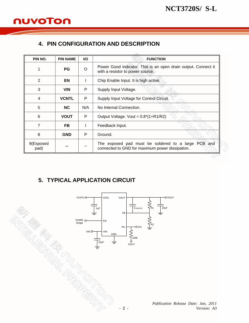
4. PIN CONFIGURATION AND DESCRIPTION
PIN NO. PIN NAME I/O FUNCTION
1 PG O Power Good indicator. This is an open drain output. Connect it with a resistor to power source.
2 EN I Chip Enable Input. It is high active.
3 VIN P Supply Input Voltage.
4 VCNTL P Supply Input Voltage for Control Circuit.
5 NC N/A No Internal Connection.
6 VOUT P Output Voltage. Vout = 0.8*(1+R1/R2)
7 FB I Feedback Input.
8 GND P Ground.
9(Exposed pad)
-- -- The exposed pad must be soldered to a large PCB and connected to GND for maximum power dissipation.
5. TYPICAL APPLICATION CIRCUIT
CNTL
EN
VINGND
PG
FB
VOUT
1uF
10uF
100k
R1
R2
C(optional) 10uF
Enable
Singal
VCNTL
VIN
PG
VOUT
VOUT

NCT3720S/ S-L
Publication Release Date: Jan, 2011
- 3 - Version: A3
6. BLOCK DIAGRAM
Driver
OTP OCP
POR
Softstart &
Control Logic
0.8V
0.72V
PG
VOUT
VINCNTLENGND
FB
7. FUNCTIONAL DESCRIPTION
The NCT3720S/S-L is intended for applications where high current capability and very low
dropout voltage are required. It provides a very simple, low cost solution that uses very little pcb
real estate. Additional features include an enable pin to allow for a very low power consumption at
disable, and a fully adjustable output.
Output Voltage Selection
The output voltage of NCT3720S/S-L is adjustable from 0.8V to (VIN-VDROP) by external voltage
divider resisters as shown in Typical Application Circuit. The value of resisters R1 and R2 should
be more than 10kΩ to reduce the power loss. The VCNTL must be greater than (VOUT + 1.5V).
Input capacitor
NCT3720S/ S-L
Publication Release Date: Jan, 2011
- 4 - Version: A3
A minimum of 10uF ceramic capacitor is recommended to be placed directly next to the VIN pin.
This allows for the device being some distance from any bulk capacitance on the rail. Additionally,
bulk capacitance of about ≧10uF may be added closely to the input supply pin of the
NCT3720S/S-L to ensure that VIN does not sag, improving load transient response.
Output capacitor
A minmum bulk capacitance of ≧ 10uF, along with a 0.1uF ceramic decoupling capacitor is
recommended. Increaseing the bulk capacitance will improve the overall transient response. The
use of multiple lower value ceramic capacitors in parallel to achieve the desired bulk capacitance
will not cause stability issues. Although designed for use with ceramic output capacitors, the
NCT3720S/S-L is extremely tolerant of output capacitor ESR values and thus will also work
comfortably with tantalum output capacitors.
Noise immunity
In very electrically noisy environments, it is recommended that 0.1uF ceramic capacitors be
placed from VIN to GND and VOUT to GND as close to device pins as possible.
Power Good
The power good function is an open-drain output. Connects 100kΩ pull up resistor to VOUT to
obtain an output voltage. The PG pin will output high immediately after the output voltage arrives
90% of normal output voltage. The PG pin will output high with typical 4ms delay time.
Enable
The NCT3720S/S-L goes into shutdown mode when the EN pin is in the logic low condition.
During this condition, the pass transistor, error amplifier, and band gap are turned off, reducing
the supply current to 10uA typical. If the EN pin is floating, NCT3720S and NCT3720S-L
operating behaviors are different. For NCT3720S, the EN pin function pulls high level internally.
So the regulator will be turn on when EN pin is floating. As for NCT3720S-L, the EN pin function
pulls low level internally. So the regulator will be turn off when EN pin is floating.
Current Limit
The NCT3720S/S-L contains an independent current limit and the short circuit current protection
to prevent unexpected applications. The current limit monitors and controls the pass transistor’s
gate voltage, limiting the output current while higher than 3A typical. When the output voltage is
less than 0.25V, the short circuit current protection starts the current fold back function and
NCT3720S/ S-L
Publication Release Date: Jan, 2011
- 5 - Version: A3
maintains the loading current 1.5A. The output can be shorted to ground indefinitely without
damaging the part.
Thermal Consideration
The NCT3720S/S-L has a thermal shutdown circuitry to limit the junction temperature. When the
junction temperature exceeds 150C, the thermal shutdown circuit disables the output, allowing
the device to cool down. The output circuitry is enabled again after the junction temperature cools
down by 30C, resulting in a pulsed output during continuous thermal overload conditions. The
thermal protection is designed to protect the IC in the event of over temperature conditions. For
reliabile operation, the junction temperature cannot exceed 125C.
The definition of power dissipation in chip is as following equation:
PD = (VIN - VOUT) x IOUT + VIN x IQ
PD represents the power dissipation.
The power dissipation depends on the thermal resistance of chip package, PCB layout, the
airflow and temperature difference between junction and ambient. Refers to JEDEC51-1, The
power dissipation can be calculated by following equation:
PD(MAX) = (TJ(MAX) - TA) / θJA
Where TJ(MAX) is the maximum operation junction temperature 125℃ , TA is the ambient
temperature and theθJA is the junction to ambient thermal resistance. θJA for ESOP-8 package
is 75℃/W on JEDEC51-7 (4 layers, 2S2P) thermal test board with minimum copper area. The
maximum power dissipation at TA = 25℃ can be calculated as:
PD(MAX) = (125℃ - 25℃) / 75℃/W = 1.33W
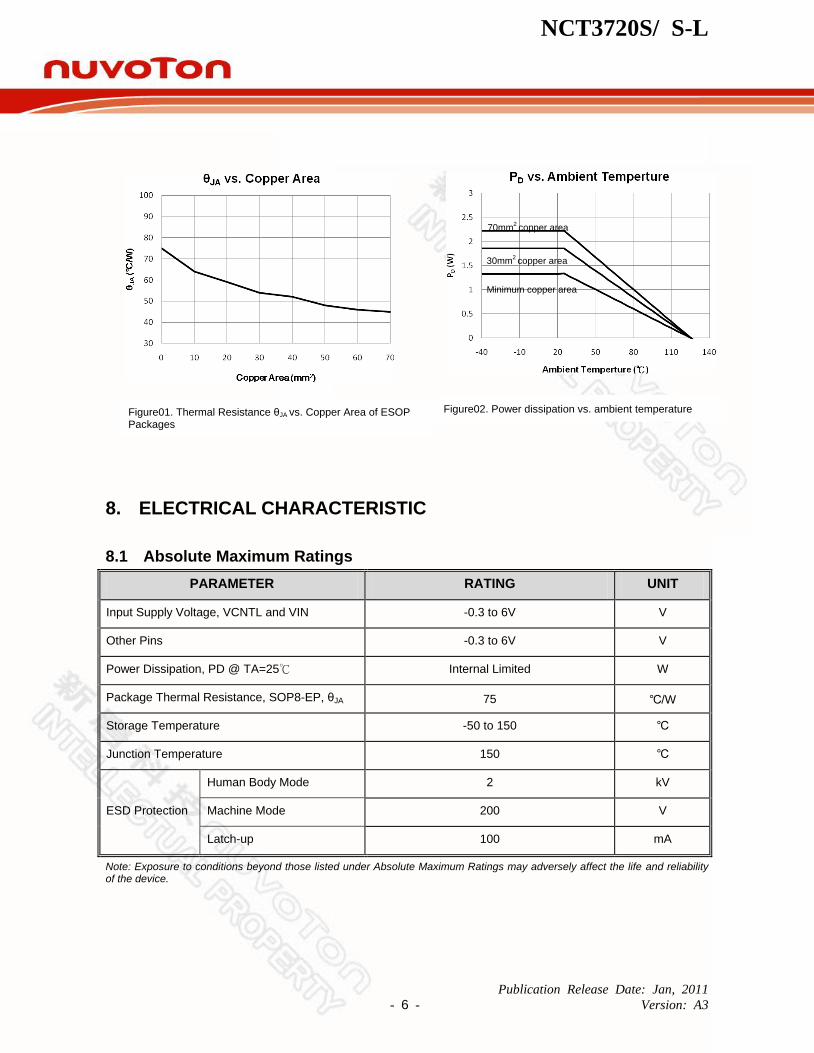
θJA highly depends on IC package, PCB layout, the aireflow. Thermal resistanceθJA can be
improved by adding copper under the exposed pad of ESOP-8 while the IC package is fixed. The
copper under the exposed pad of ESOP-8 is an effective heatsink and is useful for improving
thermal conductivity. Figure show the relationship between thermal resistance θJA vs. copper
area on a standard JEDEC 51-7 (4 layers, 2S2P) thermal test board at TA = 25℃, PCB copper
thickness = 2oz. The 70mm2 copper plane reduceθJA from 75℃/W to 45℃/W and increases
maximum power disspation from 1.33W to 2.22W.
NCT3720S/ S-L
Publication Release Date: Jan, 2011
- 6 - Version: A3
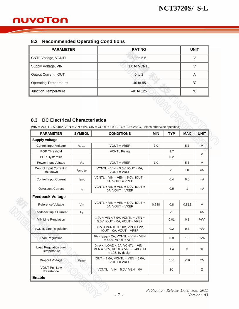
8. ELECTRICAL CHARACTERISTIC
8.1 Absolute Maximum Ratings
PARAMETER RATING UNIT
Input Supply Voltage, VCNTL and VIN -0.3 to 6V V
Other Pins -0.3 to 6V V
Power Dissipation, PD @ TA=25℃ Internal Limited W
Package Thermal Resistance, SOP8-EP, θJA 75 ℃/W
Storage Temperature -50 to 150 ℃
Junction Temperature 150 ℃
ESD Protection
Human Body Mode 2 kV
Machine Mode 200 V
Latch-up 100 mA
Note: Exposure to conditions beyond those listed under Absolute Maximum Ratings may adversely affect the life and reliability of the device.
Figure02. Power dissipation vs. ambient temperature Figure01. Thermal Resistance θJA vs. Copper Area of ESOP Packages
Minimum copper area
30mm2 copper area
70mm2 copper area
NCT3720S/ S-L
Publication Release Date: Jan, 2011
- 7 - Version: A3
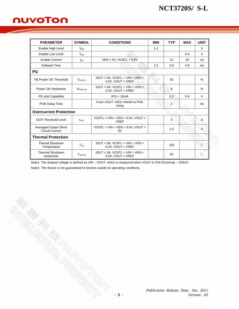
8.2 Recommended Operating Conditions
PARAMETER RATING UNIT
CNTL Voltage, VCNTL 3.0 to 5.5 V
Supply Voltage, VIN 1.0 to VCNTL V
Output Current, IOUT 0 to 2 A
Operating Temperature -40 to 85 ℃
Junction Temperature -40 to 125 ℃
8.3 DC Electrical Characteristics
(VIN = VOUT + 500mV, VEN = VIN = 5V, CIN = COUT = 10uF, TA = TJ = 25 C, unless otherwise specified)
PARAMETER SYMBOL CONDITIONS MIN TYP MAX UNIT
Supply voltage
Control Input Voltage VCNTL VOUT = VREF 3.0 5.5 V
POR Threshold VCNTL Rising 2.7 V
POR Hysteresis 0.2
Power Input Voltage VIN VOUT = VREF 1.0 5.5 V
Control Input Current in shutdown
ICNTL_SD VCNTL = VIN = 5.0V, IOUT = 0A,
VOUT = VREF 20 30 uA
Control Input Current ICNTL VCNTL = VIN = VEN = 5.0V, IOUT =
0A, VOUT = VREF 0.4 0.6 mA
Quiescent Current IQ VCNTL = VIN = VEN = 5.0V, IOUT =
0A, VOUT = VREF 0.6 1 mA
Feedback Voltage
Reference Voltage VFB VCNTL = VIN = VEN = 5.0V, IOUT =
0A, VOUT = VREF 0.788 0.8 0.812 V
Feedback Input Current IFB 20 nA
VIN Line Regulation 1.2V < VIN < 5.0V, VCNTL = VEN =
5.0V, IOUT = 0A, VOUT = VREF 0.01 0.1 %/V
VCNTL Line Regulation 3.0V < VCNTL < 5.0V, VIN = 1.2V,
IOUT = 0A, VOUT = VREF 0.2 0.6 %/V
Load Regulation 0A < ILOAD < 2A, VCNTL = VIN = VEN
= 5.0V, VOUT = VREF 0.8 1.5 %/A
Load Regulation over Temperature
0mA < ILOAD < 2A, VCNTL = VIN =
VEN = 5.0V, VOUT = VREF, -40 < TJ < 125, by design
1.4 3 %
Dropout Voltage VDROP IOUT = 2.0A, VCNTL = VEN = 5.0V,
VOUT = VREF 150 250 mV
VOUT Pull Low Resistance
VCNTL = VIN = 5.0V, VEN = 0V 90 Ω
Enable
NCT3720S/ S-L
Publication Release Date: Jan, 2011
- 8 - Version: A3
PARAMETER SYMBOL CONDITIONS MIN TYP MAX UNIT
Enable High Level VEN 1.4 V
Enable Low Level VSD 0.4 V
Enable Current IEN VEN = 0V, VCNTL = 5.0V 12 20 uA
Softstart Time 1.5 3.0 4.5 ms
PG
FB Power OK Threshold VPOKTH IOUT = 0A, VCNTL = VIN = VEN =
5.0V, VOUT = VREF 92 %
Power OK Hysteresis VPOKHYS IOUT = 0A, VCNTL = VIN = VEN =
5.0V, VOUT = VREF 8 %
PG sink Capability IPG = 10mA 0.2 0.4 V
POK Delay Time From VOUT >92% VNOM to POK
rising 3 ms
Overcurrent Protection
OCP Threshold Level IOCP VCNTL = VIN = VEN = 5.0V, VOUT =
VREF 4 A
Averaged Output Short Circuit Current
VCNTL = VIN = VEN = 5.0V, VOUT =
0V 1.5 A
Thermal Protection
Themal Shutdown Temperature
TSD IOUT = 0A, VCNTL = VIN = VEN =
5.0V, VOUT = VREF 150 ℃
Thermal Shutdown Hysteresis
TSDHYS IOUT = 0A, VCNTL = VIN = VEN =
5.0V, VOUT = VREF 50 ℃
Note1. The dropout voltage is defined as VIN – VOUT, which is measured when VOUT is VOUT(normal) – 100mV.
Note2. The device is not guaranteed to function ouside its operating conditions.

NCT3720S/ S-L
Publication Release Date: Jan, 2011
- 9 - Version: A3
9. TYPICAL OPERATING WAVEFORMS (VIN = VOUT + 0.5V, VCNTL = VEN = 5V, CIN = COUT=10uF, CVCNTL = 1uF, TA = 25℃ )
Power On Power Off
Enable Disable
Transient Response UVLO

NCT3720S/ S-L
Publication Release Date: Jan, 2011
- 10 - Version: A3

NCT3720S/ S-L
Publication Release Date: Jan, 2011
- 11 - Version: A3
10. PACKAGE DIMENSION
SOP8-EP (150mil)
Min Max Min MaxA 1.35 1.75 0.05 0.07A1 0.05 0.25 0.00 0.01b 0.31 0.51 0.01 0.02c 0.1 0.25 0.00 0.01D 4.7 5.10 0.19 0.2E 3.8 4.00 0.15 0.16eHe 5.8 6.20 0.23 0.24Y - 0.10 - 0.00L 0.4 1.27 0.02 0.05θ 0° 10° 0° 10°D1 3.10 3.50 0.12 0.14E1 2.20 2.60 0.09 0.10
SYMBOLSDimensions In Millimeters Dimensions In Inched
1.27 BASIC 0.05 BASIC

NCT3720S/ S-L
Publication Release Date: Jan, 2011
- 12 - Version: A3
10.1 Taping Specification
11. ORDERING INFORMATION
12. TOP MARKING SPECIFICATION
1st Line: Nuvoton logo
2nd
Line: 3720S (Part number NCT3720S); 3720L (Part number NCT3720S-L)
3rd
line: Tracking code
952: packages assembled in Year 2009, week 52
A: assembly house ID
X: internal use only
Part Number Package Type Supplied as Production Flow
NCT3720S SOP8-EP (Green Package) 2,500 units/T&R Commercial, -40℃ to 85℃
NCT3720S-L SOP8-EP (Green Package) 2,500 units/T&R Commercial, -40℃ to 85℃
SOP8-EP Package
Pin 1 index
3 7 2 0 S 9 5 2 A X
Pin 1 index
3 7 2 0 L 9 5 2 A X

NCT3720S/ S-L
Publication Release Date: Jan, 2011
- 13 - Version: A3
13. REVISION HISTORY
VERSION DATE PAGE DESCRIPTION
A0 09/30/2010 All New Create
A1 11/26/2010 All Add NCT3720S-L part number and relative data.
A2 01/18/2011 P12 & P13 Added part numbers and relative data.
A3 01/20/2011 P1, P9, P10, P12 & P13
Added waveform and revised some description. Removed part numbers and relative data.
Important Notice
Nuvoton Products are neither intended nor warranted for usage in systems or equipment, any malfunction or failure of which may cause loss of human life, bodily injury or severe property damage. Such applications are deemed, “Insecure Usage”.
Insecure usage includes, but is not limited to: equipment for surgical implementation, atomic energy control instruments, airplane or spaceship instruments, the control or operation of dynamic, brake or safety systems designed for vehicular use, traffic signal instruments, all types of safety devices, and other applications intended to support or sustain life.
All Insecure Usage shall be made at customer’s risk, and in the event that third parties lay claims to Nuvoton as a result of customer’s Insecure Usage, customer shall indemnify the damages and liabilities thus incurred by Nuvoton.