nvp2120 datasheet ver0 eng - fscctv.com.t · 21 afe_scl o 3-wire serial interface clock output (for...
TRANSCRIPT
NVP2120 Data Sheet
CCD Image Signal Processor
Information contained here is subject to change without notice.Make sure to check and use an updated version of the Data Sheet.
www.nextchip.com
2007.03.12
REV 0.0

CONFIDENTIAL
SWITRON
NVP2120 CCD Image Signal Processor
Data sheet03.12.2007 (REV 0.0)
2/43
CCD Image Signal Processor
NVP2120 outputs CVBS or S-Video after receiving CFA patterns from the color-interlaced CCD, which are
processed through an internal encoder and DAC. Equipped with built-in AE/AWB algorithms, timing generation
module and OSD, NVP2120 can be operated without Micom. NVP2120 can support high resolution output of
520 TV lines and has enhanced BLC function and motion detection function in 64 areas.
Features
-. Input : NTSC/PAL, 510H/760H CCD format
-. Output : NTSC/PAL Analog S-Video or CVBS
ITU-R.656 Digital Out (27MHz/28.6366MHz)
-. 3-line color processing
-. Programmable GAMMA processing
-. H/V Aperture
-. Video adjustment (brightness, contrast, saturation and hue)
-. High quality color processing
-. Horizontal MIRROR
-. On Screen Display (OSD )
-. Blemish Compensation 32 points(Auto/Manual)
-. Color rolling suppress.
-. Breathing suppress.
-. Support Horizontal Resolution 520TV Lines
-. Privacy Mask 4 Zone
-. Motion detection (64 area)
-. On-chip AE/AWB
-. On-chip CCD timing generator
-. On-chip NTSC/PAL video encoder
-. On-chip DAC(S-video or CVBS)
-. I2C interface for EEPROM (Micom less camera)
-. Serial interface for AFE
-. 3.3V operation
Ordering Information
Device Package Temperature Range
NVP2120 80-TQFP 0 ~ 70
Applications
-. CCD Camera
-. Door Phone Camera
-. Video Phone Camera
-. Rear-view Monitoring Camera
Related Products
-. CCD : SONY, SHARP , PANASONIC CCD
(510H/760H)
-. AFE : AD9806,AD9943 (Analog Device)
-. V-Driver : NVD2014 (NEXTCHIP)
Functional Block Diagram
CONFIDENTIAL
SWITRON
NVP2120 CCD Image Signal Processor
Data sheet03.12.2007 (REV 0.0)
3/43
[[ Table of Contents ]]
1. Pin Information .......................................................................................................................................... 4
1.1 Pin Assignments ...........................................................................................................................4
1.2 Pin Description ..............................................................................................................................5
2. Register Description ...................................................................................................................................... 7
2.1 Register Map...................................................................................................................................7
2.1 Register Description ......................................................................................................................15
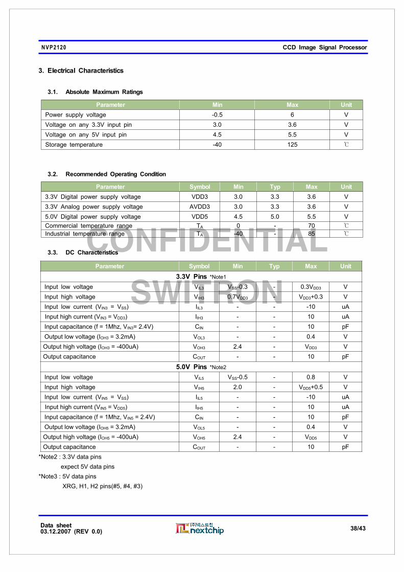
3. Electrical characteristics ............................................................................................................................... 38
3.1 Absolute Maximum Ratings ..........................................................................................................38
3.2 Recommended Operating Condition ............................................................................................38
3.3 DC Characteristics ........................................................................................................................38
4. System Application ........................................................................................................................................39
4.1 Circuit Guide ..................................................................................................................................39
4.2 Package Information ......................................................................................................................42
5. Revision History ...........................................................................................................................................43
6. Contact Information ........................................................................................................................................43
CONFIDENTIAL
SWITRON
NVP2120 CCD Image Signal Processor
Data sheet03.12.2007 (REV 0.0)
4/43
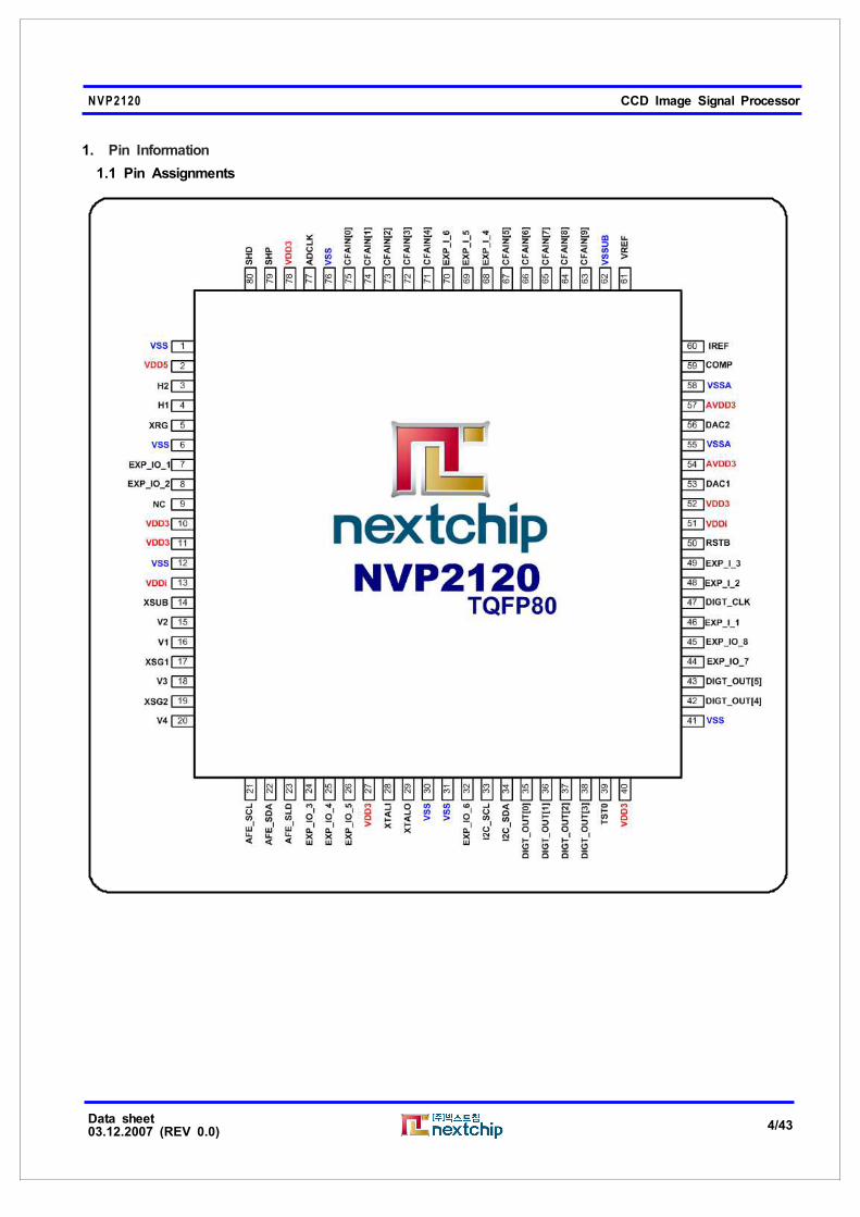
1. Pin Information
1.1 Pin Assignments

CONFIDENTIAL
SWITRON
NVP2120 CCD Image Signal Processor
Data sheet03.12.2007 (REV 0.0)
5/43
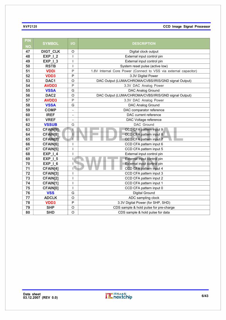
1.2 Pin Description
PIN
NO.SYMBOL I/O DESCRIPTION
1 VSS G Digital Ground (for SHP, SHD)
2 VDD5 P 5V Digital Power (for XRG, H1, H2 pulse)
3 H2 O CCD Horizontal Driving pulse 2
4 H1 O CCD Horizontal Driving pulse 1
5 XRG O CCD Reset gate pulse
6 VSS G Digital Ground (for XRG, H1, H2 pulse)
7 EXP_IO_1 I/O External input/output control pin
8 EXP_IO_2 I/O External input/output control pin
9 NC O NC
10 VDD3 P 3.3V Digital Power
11 VDD3 P 3.3V Digital Power
12 VSS G Digital Ground
13 VDDi P 1.8V Internal Core Power(Connect to VSS via external capacitor)
14 XSUB O CCD shutter speed control pulse
15 V2 O CCD vertical driving pulse phase-2
16 V1 O CCD vertical driving pulse phase-1
17 XSG1 O CCD Read out pulse 1
18 V3 O CCD vertical driving pulse phase-3
19 XSG2 O CCD Read out pulse 2
20 V4 O CCD vertical driving pulse phase-4
21 AFE_SCL O 3-wire Serial interface clock output (for AFE control)
22 AFE_SDA O 3-wire Serial data input/output (for AFE control)
23 AFE_SLD O 3-wire Serial Enable output (for AFE control)
24 EXP_IO_3 I/O External input/output control pin
25 EXP_IO_4 I/O External input/output control pin
26 EXP_IO_5 I/O External input/output control pin
27 VDD3 P 3.3V Digital Power
28 XTALI I X-tal input(NTSC:28.6363Mhz : PAL:28.375Mhz)
29 XTALO O X-tal output
30 VSS G Digital Ground
31 VSS G Digital Ground
32 EXP_IO_6 I/O External input/output control pin
33 I2C_SCL I/O Serial Clock (EEPROM/MICOM interface)
34 I2C_SDA I/O Serial Data (EEPROM/MICOM interface)
35 DIGT_OUT[0] O Digital data output [0]
36 DIGT_OUT[1] O Digital data output [1]
37 DIGT_OUT[2] O Digital data output [2]
38 DIGT_OUT[3] O Digital data output [3]
39 TST0 I Chip Test Pin
40 VDD3 P 3.3V Digital Power
41 VSS G Digital Ground
42 DIGT_OUT[4] O Digital data output [4]
43 DIGT_OUT[5] O Digital data output [5]
44 EXP_IO_7 I/O External input/output control pin
45 EXP_IO_8 I/O External input/output control pin
46 EXP_I_1 I External input control pin
CONFIDENTIAL
SWITRON
NVP2120 CCD Image Signal Processor
Data sheet03.12.2007 (REV 0.0)
6/43
PIN
NO.SYMBOL I/O DESCRIPTION
47 DIGT_CLK O Digital clock output
48 EXP_I_2 I External input control pin
49 EXP_I_3 I External input control pin
50 RSTB I System reset pulse (active low)
51 VDDi P 1.8V Internal Core Power (Connect to VSS via external capacitor)
52 VDD3 P 3.3V Digital Power
53 DAC1 O DAC Output (LUMA/CHROMA/CVBS/IRIS/GND signal Output)
54 AVDD3 P 3.3V DAC Analog Power
55 VSSA G DAC Analog Ground
56 DAC2 O DAC Output (LUMA/CHROMA/CVBS/IRIS/GND signal Output)
57 AVDD3 P 3.3V DAC Analog Power
58 VSSA G DAC Analog Ground
59 COMP - DAC comparator reference
60 IREF - DAC current reference
61 VREF - DAC Voltage reference
62 VSSUB G DAC Ground
63 CFAIN[9] I CCD CFA pattern input 9
64 CFAIN[8] I CCD CFA pattern input 8
65 CFAIN[7] I CCD CFA pattern input 7
66 CFAIN[6] I CCD CFA pattern input 6
67 CFAIN[5] I CCD CFA pattern input 5
68 EXP_I_4 I External input control pin
69 EXP_I_5 I External input control pin
70 EXP_I_6 I External input control pin
71 CFAIN[4] I CCD CFA pattern input 4
72 CFAIN[3] I CCD CFA pattern input 3
73 CFAIN[2] I CCD CFA pattern input 2
74 CFAIN[1] I CCD CFA pattern input 1
75 CFAIN[0] I CCD CFA pattern input 0
76 VSS G Digital Ground
77 ADCLK O ADC sampling clock
78 VDD3 P 3.3V Digital Power (for SHP, SHD)
79 SHP O CDS sample & hold pulse for pre-charge
80 SHD O CDS sample & hold pulse for data
CONFIDENTIAL
SWITRON
NVP2120 CCD Image Signal Processor
Data sheet03.12.2007 (REV 0.0)
7/43
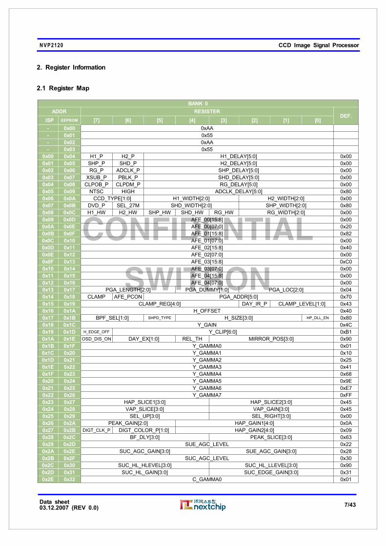
2. Register Information
2.1 Register Map
BANK 0
ADDR RESISTERDEF.
ISP EEPROM [7] [6] [5] [4] [3] [2] [1] [0]
- 0x00 0xAA
- 0x01 0x55
- 0x02 0xAA
- 0x03 0x55
0x00 0x04 H1_P H2_P H1_DELAY[5:0] 0x00
0x01 0x05 SHP_P SHD_P H2_DELAY[5:0] 0x00
0x02 0x06 RG_P ADCLK_P SHP_DELAY[5:0] 0x00
0x03 0x07 XSUB_P PBLK_P SHD_DELAY[5:0] 0x00
0x04 0x08 CLPOB_P CLPDM_P RG_DELAY[5:0] 0x00
0x05 0x09 NTSC HIGH ADCLK_DELAY[5:0] 0x80
0x06 0x0A CCD_TYPE[1:0] H1_WIDTH[2:0] H2_WIDTH[2:0] 0x00
0x07 0x0B DVD_P SEL_27M SHD_WIDTH[2:0] SHP_WIDTH[2:0] 0x80
0x08 0x0C H1_HW H2_HW SHP_HW SHD_HW RG_HW RG_WIDTH[2:0] 0x00
0x09 0x0D AFE_00[15:8] 0x00
0x0A 0x0E AFE_00[07:0] 0x20
0x0B 0x0F AFE_01[15:8] 0x82
0x0C 0x10 AFE_01[07:0] 0x00
0x0D 0x11 AFE_02[15:8] 0x40
0x0E 0x12 AFE_02[07:0] 0x00
0x0F 0x13 AFE_03[15:8] 0xC0
0x10 0x14 AFE_03[07:0] 0x00
0x11 0x15 AFE_04[15:8] 0x00
0x12 0x16 AFE_04[07:0] 0x00
0x13 0x17 PGA_LENGTH[2:0] PGA_DUMMY[1:0] PGA_LOC[2:0] 0x04
0x14 0x18 CLAMP AFE_PCON PGA_ADDR[5:0] 0x70
0x15 0x19 CLAMP_REG[4:0] DAY_IR_P CLAMP_LEVEL[1:0] 0x43
0x16 0x1A H_OFFSET 0x40
0x17 0x1B BPF_SEL[1:0] SHPD_TYPE H_SIZE[3:0] HP_DLL_EN 0x80
0x18 0x1C Y_GAIN 0x4C
0x19 0x1D H_EDGE_OFF Y_CLIP[6:0] 0xB1
0x1A 0x1E OSD_DIS_ON DAY_EX[1:0] REL_TH MIRROR_POS[3:0] 0x90
0x1B 0x1F Y_GAMMA0 0x01
0x1C 0x20 Y_GAMMA1 0x10
0x1D 0x21 Y_GAMMA2 0x25
0x1E 0x22 Y_GAMMA3 0x41
0x1F 0x23 Y_GAMMA4 0x68
0x20 0x24 Y_GAMMA5 0x9E
0x21 0x25 Y_GAMMA6 0xE7
0x22 0x26 Y_GAMMA7 0xFF
0x23 0x27 HAP_SLICE1[3:0] HAP_SLICE2[3:0] 0x45
0x24 0x28 VAP_SLICE[3:0] VAP_GAIN[3:0] 0x45
0x25 0x29 SEL_UP[3:0] SEL_RIGHT[3:0] 0x00
0x26 0x2A PEAK_GAIN[2:0] HAP_GAIN1[4:0] 0x0A
0x27 0x2B DIGT_CLK_P DIGT_COLOR_P[1:0] HAP_GAIN2[4:0] 0x09
0x28 0x2C BF_DLY[3:0] PEAK_SLICE[3:0] 0x63
0x29 0x2D SUE_AGC_LEVEL 0x22
0x2A 0x2E SUC_AGC_GAIN[3:0] SUE_AGC_GAIN[3:0] 0x28
0x2B 0x2F SUC_AGC_LEVEL 0x30
0x2C 0x30 SUC_HL_HLEVEL[3:0] SUC_HL_LLEVEL[3:0] 0x90
0x2D 0x31 SUC_HL_GAIN[3:0] SUC_EDGE_GAIN[3:0] 0x31
0x2E 0x32 C_GAMMA0 0x01
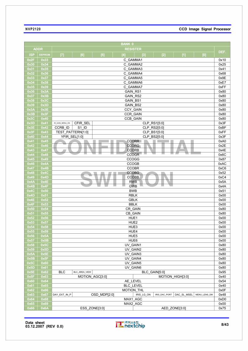
CONFIDENTIAL
SWITRON
NVP2120 CCD Image Signal Processor
Data sheet03.12.2007 (REV 0.0)
8/43
BANK 0
ADDR RESISTERDEF.
ISP EEPROM [7] [6] [5] [4] [3] [2] [1] [0]
0x2F 0x33 C_GAMMA1 0x10
0x30 0x34 C_GAMMA2 0x25
0x31 0x35 C_GAMMA3 0x41
0x32 0x36 C_GAMMA4 0x68
0x33 0x37 C_GAMMA5 0x9E
0x34 0x38 C_GAMMA6 0xE7
0x35 0x39 C_GAMMA7 0xFF
0x36 0x3A GAIN_RS1 0x80
0x37 0x3B GAIN_RS2 0x80
0x38 0x3C GAIN_BS1 0x80
0x39 0x3D GAIN_BS2 0x80
0x3A 0x3E CCY_GAIN 0x80
0x3B 0x3F CCR_GAIN 0x80
0x3C 0x40 CCB_GAIN 0x80
0x3D 0x41 IR_GAIN_MENU_ON CFIR_SEL CLP_RS1[5:0] 0x3F
0x3E 0x42 CCRB_ID S1_ID CLP_RS2[5:0] 0xBF
0x3F 0x43 TEST_PATTERN[1:0] CLP_BS1[5:0] 0xFF
0x40 0x44 YFIR_SEL[1:0] CLP_BS2[5:0] 0x3F
0x41 0x45 CCORR 0xA0
0x42 0x46 CCORG 0x2E
0x43 0x47 CCORB 0x4E
0x44 0x48 CCOGR 0x6C
0x45 0x49 CCOGG 0x87
0x46 0x4A CCOGB 0xAC
0x47 0x4B CCOBR 0xC6
0x48 0x4C CCOBG 0x52
0x49 0x4D CCOBB 0xC4
0x4A 0x4E RWB 0x5A
0x4B 0x4F GWB 0x4A
0x4C 0x50 BWB 0x51
0x4D 0x51 RBLK 0x00
0x4E 0x52 GBLK 0x00
0x4F 0x53 BBLK 0x00
0x50 0x54 CR_GAIN 0x80
0x51 0x55 CB_GAIN 0x80
0x52 0x56 HUE1 0x00
0x53 0x57 HUE2 0x00
0x54 0x58 HUE3 0x00
0x55 0x59 HUE4 0x00
0x56 0x5A HUE5 0x00
0x57 0x5B HUE6 0x00
0x58 0x5C UV_GAIN1 0x80
0x59 0x5D UV_GAIN2 0x80
0x5A 0x5E UV_GAIN3 0x80
0x5B 0x5F UV_GAIN4 0x80
0x5C 0x60 UV_GAIN5 0x80
0x5D 0x61 UV_GAIN6 0x80
0x5E 0x62 BLC BLC_AREA_VIEW BLC_GAIN[5:0] 0x95
0x5F 0x63 MOTION_AGC[3:0] MOTION_HIGH[3:0] 0x40
0x60 0x64 AE_LEVEL 0x54
0x61 0x65 BLC_LEVEL 0x40
0x62 0x66 MOTION_THL 0x0F
0x63 0x67 DAY_EXT_IN_P OSD_MDP[2:0] IRIS_LG_ON IRIS_DAC_PORT DAC_SL_MSEL MENU_LENS_DM 0x48
0x64 0x68 MAX1_AGC 0xD0
0x65 0x69 MAX2_AGC 0x00
0x66 0x6A ESS_ZONE[3:0] AED_ZONE[3:0] 0x75

CONFIDENTIAL
SWITRON
NVP2120 CCD Image Signal Processor
Data sheet03.12.2007 (REV 0.0)
9/43
BANK 0
ADDR RESISTERDEF.
ISP EEPROM [7] [6] [5] [4] [3] [2] [1] [0]
0x67 0x6B ESS_SDLY[3:0] AGC_SDLY[3:0] 0x00
0x68 0x6C AE_DG_REG[9:8] AGC_REG[9:8] AE_SPD[3:0] 0x4F
0x69 0x6D AE_DG_REG[7:0] 0x00
0x6A 0x6E AGC_REG[7:0] 0x00
0x6B 0x6F AE_MODE[1:0] SSM[2:0] MOTION_TEST IRIS_LENS[1:0] 0x42
0x6C 0x70 BTN_REPT_ON OSD_TRANS[1:0] ME_ESS[12:8] 0xE0
0x6D 0x71 ME_ESS[7:0] 0x15
0x6E 0x72 R_MAX 0x8D
0x6F 0x73 B_MAX 0x43
0x70 0x74 R_MIN 0x64
0x71 0x75 B_MIN 0xCB
0x72 0x76 AWB_HIGH 0xF0
0x73 0x77 AWB_MODE[1:0] AWB_DIP[1:0] PZ_STATE[3:0] 0x40
0x74 0x78 AWB_LOW 0x07
0x75 0x79 R_CLP[3:0] B_CLP[3:0] 0xFF
0x76 0x7A INTVAL_H[3:0] INTVAL_L[3:0] 0x44
0x77 0x7B AWB_SPD[3:0] STA_ZONE[3:0] 0xF4
0x78 0x7C STA_IN_LMT[3:0] STA_OUT_LMT[3:0] 0x11
0x79 0x7D SEL_EXPO_02[3:0] SEL_EXPO_01[3:0] 0x00
0x7A 0x7E AWB_R0 0x40
0x7B 0x7F AWB_R1 0x04
0x7C 0x80 AWB_R2 0x6D
0x7D 0x81 AWB_R3 0x42
0x7E 0x82 AWB_B0 0x40
0x7F 0x83 AWB_B1 0x00
0x80 0x84 AWB_B2 0xEE
0x81 0x85 AWB_B3 0x3C
0x82 0x86 AWB_R_OFFSET 0x10
0x83 0x87 AWB_B_OFFSET 0x08
0x84 0x88 DAY_NIGHT_START 0xC3
0x85 0x89 DAY_NIGHT_END 0x97
0x86 0x8A DAY_ON[1:0] DAY_DLY[5:0] 0x41
0x87 0x8B SEL_EXPO_04[3:0] SEL_EXPO_03[3:0] 0x00
0x88 0x8C SEL_EXPO_06[3:0] SEL_EXPO_05[3:0] 0x00
0x89 0x8D SEL_EXPO_08[3:0] SEL_EXPO_07[3:0] 0x00
0x8A 0x8E MBK_ON MENU_BKSEL[1:0] SC_OFFSET[4:0] 0x00
0x8B 0x8F DEF_M_SEL[4:0] MENU_BTN3 DAY_EXT_IN_REG DFLD_P 0x04
0x8C 0x90 HXV_OFFSET 0x00
0x8D 0x91 PRE_Y_GAIN 0x80
0x8E 0x92 EDGE_S[3:0] EDGE_E[3:0] 0x02
0x8F 0x93 PZ_ON MOTION_EN M_VIEW_ON DAY_BURST_ON PZ_COLOR[3:0] 0x58
0x90 0x94 PZ_SH0 0x18
0x91 0x95 PZ_SV0 0x10
0x92 0x96 PZ_EH0 0x30
0x93 0x97 PZ_EV0 0x30
0x94 0x98 PZ_SH1 0x50
0x95 0x99 PZ_SV1 0x10
0x96 0x9A PZ_EH1 0x68
0x97 0x9B PZ_EV1 0x30
0x98 0x9C PZ_SH2 0x18
0x99 0x9D PZ_SV2 0x40
0x9A 0x9E PZ_EH2 0x30
0x9B 0x9F PZ_EV2 0x60
0x9C 0xA0 PZ_SH3 0x50
0x9D 0xA1 PZ_SV3 0x40
0x9E 0xA2 PZ_EH3 0x68
CONFIDENTIAL
SWITRON
NVP2120 CCD Image Signal Processor
Data sheet03.12.2007 (REV 0.0)
10/43
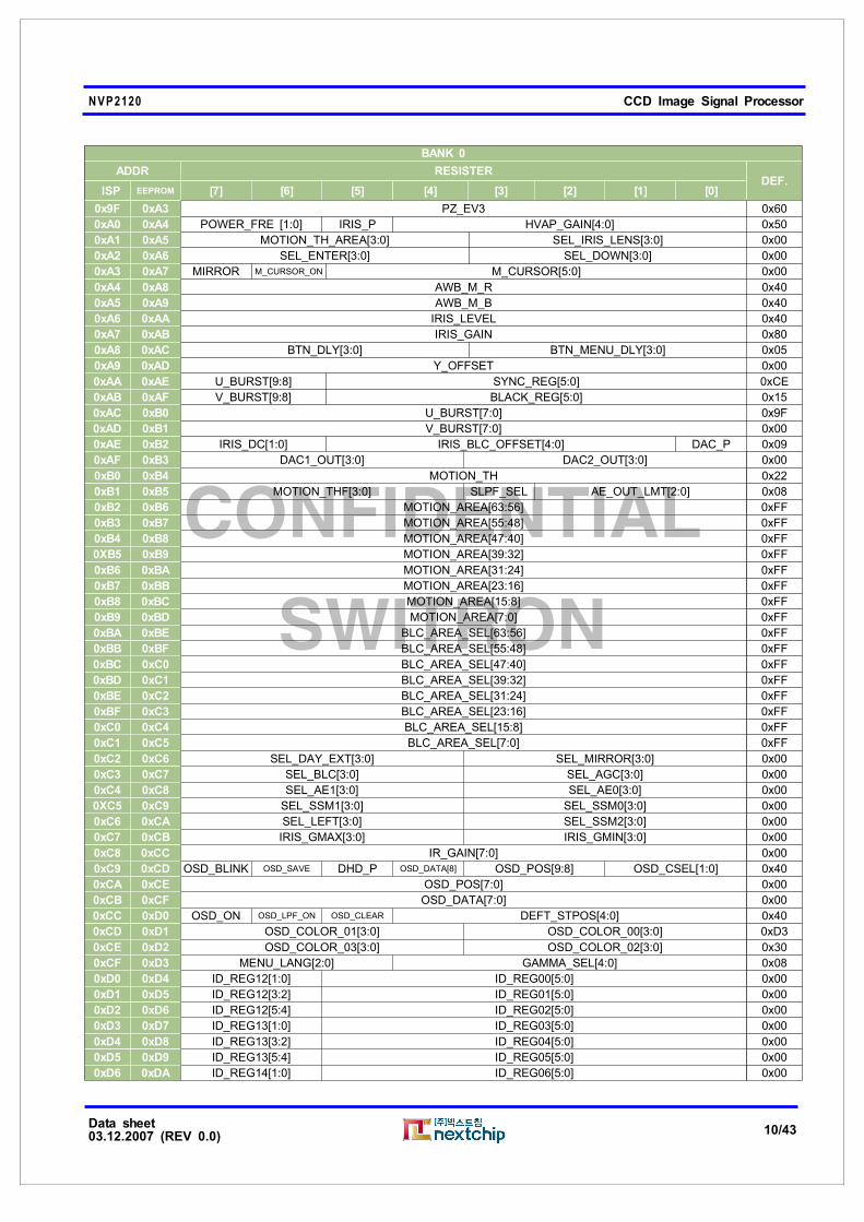
BANK 0
ADDR RESISTERDEF.
ISP EEPROM [7] [6] [5] [4] [3] [2] [1] [0]
0x9F 0xA3 PZ_EV3 0x60
0xA0 0xA4 POWER_FRE [1:0] IRIS_P HVAP_GAIN[4:0] 0x50
0xA1 0xA5 MOTION_TH_AREA[3:0] SEL_IRIS_LENS[3:0] 0x00
0xA2 0xA6 SEL_ENTER[3:0] SEL_DOWN[3:0] 0x00
0xA3 0xA7 MIRROR M_CURSOR_ON M_CURSOR[5:0] 0x00
0xA4 0xA8 AWB_M_R 0x40
0xA5 0xA9 AWB_M_B 0x40
0xA6 0xAA IRIS_LEVEL 0x40
0xA7 0xAB IRIS_GAIN 0x80
0xA8 0xAC BTN_DLY[3:0] BTN_MENU_DLY[3:0] 0x05
0xA9 0xAD Y_OFFSET 0x00
0xAA 0xAE U_BURST[9:8] SYNC_REG[5:0] 0xCE
0xAB 0xAF V_BURST[9:8] BLACK_REG[5:0] 0x15
0xAC 0xB0 U_BURST[7:0] 0x9F
0xAD 0xB1 V_BURST[7:0] 0x00
0xAE 0xB2 IRIS_DC[1:0] IRIS_BLC_OFFSET[4:0] DAC_P 0x09
0xAF 0xB3 DAC1_OUT[3:0] DAC2_OUT[3:0] 0x00
0xB0 0xB4 MOTION_TH 0x22
0xB1 0xB5 MOTION_THF[3:0] SLPF_SEL AE_OUT_LMT[2:0] 0x08
0xB2 0xB6 MOTION_AREA[63:56] 0xFF
0xB3 0xB7 MOTION_AREA[55:48] 0xFF
0xB4 0xB8 MOTION_AREA[47:40] 0xFF
0XB5 0xB9 MOTION_AREA[39:32] 0xFF
0xB6 0xBA MOTION_AREA[31:24] 0xFF
0xB7 0xBB MOTION_AREA[23:16] 0xFF
0xB8 0xBC MOTION_AREA[15:8] 0xFF
0xB9 0xBD MOTION_AREA[7:0] 0xFF
0xBA 0xBE BLC_AREA_SEL[63:56] 0xFF
0xBB 0xBF BLC_AREA_SEL[55:48] 0xFF
0xBC 0xC0 BLC_AREA_SEL[47:40] 0xFF
0xBD 0xC1 BLC_AREA_SEL[39:32] 0xFF
0xBE 0xC2 BLC_AREA_SEL[31:24] 0xFF
0xBF 0xC3 BLC_AREA_SEL[23:16] 0xFF
0xC0 0xC4 BLC_AREA_SEL[15:8] 0xFF
0xC1 0xC5 BLC_AREA_SEL[7:0] 0xFF
0xC2 0xC6 SEL_DAY_EXT[3:0] SEL_MIRROR[3:0] 0x00
0xC3 0xC7 SEL_BLC[3:0] SEL_AGC[3:0] 0x00
0xC4 0xC8 SEL_AE1[3:0] SEL_AE0[3:0] 0x00
0XC5 0xC9 SEL_SSM1[3:0] SEL_SSM0[3:0] 0x00
0xC6 0xCA SEL_LEFT[3:0] SEL_SSM2[3:0] 0x00
0xC7 0xCB IRIS_GMAX[3:0] IRIS_GMIN[3:0] 0x00
0xC8 0xCC IR_GAIN[7:0] 0x00
0xC9 0xCD OSD_BLINK OSD_SAVE DHD_P OSD_DATA[8] OSD_POS[9:8] OSD_CSEL[1:0] 0x40
0xCA 0xCE OSD_POS[7:0] 0x00
0xCB 0xCF OSD_DATA[7:0] 0x00
0xCC 0xD0 OSD_ON OSD_LPF_ON OSD_CLEAR DEFT_STPOS[4:0] 0x40
0xCD 0xD1 OSD_COLOR_01[3:0] OSD_COLOR_00[3:0] 0xD3
0xCE 0xD2 OSD_COLOR_03[3:0] OSD_COLOR_02[3:0] 0x30
0xCF 0xD3 MENU_LANG[2:0] GAMMA_SEL[4:0] 0x08
0xD0 0xD4 ID_REG12[1:0] ID_REG00[5:0] 0x00
0xD1 0xD5 ID_REG12[3:2] ID_REG01[5:0] 0x00
0xD2 0xD6 ID_REG12[5:4] ID_REG02[5:0] 0x00
0xD3 0xD7 ID_REG13[1:0] ID_REG03[5:0] 0x00
0xD4 0xD8 ID_REG13[3:2] ID_REG04[5:0] 0x00
0xD5 0xD9 ID_REG13[5:4] ID_REG05[5:0] 0x00
0xD6 0xDA ID_REG14[1:0] ID_REG06[5:0] 0x00

CONFIDENTIAL
SWITRON
NVP2120 CCD Image Signal Processor
Data sheet03.12.2007 (REV 0.0)
11/43
BANK 0
ADDR RESISTERDEF.
ISP EEPROM [7] [6] [5] [4] [3] [2] [1] [0]
0xD7 0xDB ID_REG14[3:2] ID_REG07[5:0] 0x00
0xD8 0xDC ID_REG14[5:4] ID_REG08[5:0] 0x00
0xD9 0xDD ID_POS_Y[1:0] ID_REG09[5:0] 0x00
0xDA 0xDE ID_POS_Y[3:2] ID_REG10[5:0] 0x00
0xDB 0xDF ID_POS_X[1:0] ID_REG11[5:0] 0x00
0xDC 0xE0 MAX_AGC_SEL OSD_ID_ON BLINK_TIME[1:0] ID_POS_Y[4] ID_POS_X[4:2] 0xD9
0xDD 0xE1 DAY_MOTOR_P DAY_PULSE_SEL[1:0] POS_LEN[4:0] 0x81
0xDE 0xE2 MENU_ICON_OFF MENU_OFF_TIME[1:0] POS_SHT[4:0] 0x62
0xDF 0xE3 DIGT_OUT BLK_TH[1:0] POS_BLC[4:0] 0x03
0xE0 0xE4 NEGATIVE_IMG BLK_GAIN[1:0] POS_AGC[4:0] 0x04
0xE1 0xE5 HPF_SEL HAP_CLIP1[1:0] POS_WBL[4:0] 0xE5
0xE2 0xE6 OSD_OLEN VAP_CLIP[1:0] POS_FNC[4:0] 0x66
0xE3 0xE7 AWB_AE_DETECT AWB_METHOD1[1:0] POS_ADJ[4:0] 0x87
0xE4 0xE8 AWB_TR_CLIP AWB_METHOD2[1:0] POS_LGG[4:0] 0xF2
0xE5 0xE9 AWB_METHOD3 AE_GMAX[1:0] POS_CID[4:0] 0x4C
0xE6 0xEA MENU_LOGO_OFF 1'b0 HAP_SUP_SEL POS_MIR[4:0] 0x2D
0xE7 0xEB DYC_RANGE MENU_BKT[1:0] POS_DAY[4:0] 0xCE
0xE8 0xEC AFE_DAC2_ON DEF_FA_ON BTN_P POS_MOT[4:0] 0x0F
0xE9 0xED DEF_FA_VALUE[2:0] POS_PRI[4:0] 0x70
0xEA 0xEE OSD_MOLEN Y_CLIP_TH[1:0] POS_GAM[4:0] 0x11
0xEB 0xEF MOTION_DELAY[1:0] MENU_IRIS_GAIN_P POS_DEF[4:0] 0x93
0xEC 0xF0 CLPOB_SIZE[3:0] CLPOB_POS[3:0] 0x88
0xED 0xF1 MENU_SH0[7:0] 0x14
0xEE 0xF2 MENU_EH0[7:0] 0x6C
0xEF 0xF3 MENU_SV0[7:0] 0x0F
0xF0 0xF4 AFE_DAC1_ON IRIS_AFE_DC INIT_SCR ADC_SET SLAVE_ADDR[3:0] 0x05
0xF1 0xF5 bank_reg 0x00
0xF2 0xF6 MENU_EV0[7:0] 0x20
0xF3 0xF7 MENU_SH1[7:0] 0x14
0xF4 0xF8 MENU_EH1[7:0] 0x6C
0xF5 0xF9 MENU_SV1[7:0] 0x21
0xF6 0xFA MENU_EV1[7:0] 0x6A
0xF7 0xFB MENU_BKC1[3:0] MENU_BKC0[3:0] 0x07
0xF8 0xFC test1 DAC1_SL DAC2_SL 1'b0 0x18
0xF9 0xFD SD_H1[1:0] SL_H1 SD_H2[1:0] 1'b0 SL_H2 1'b0 0x00
0xFA 0xFE SD_RG[1:0] SL_RG HAP_SUPPRESS[4:0] 0x00

CONFIDENTIAL
SWITRON
NVP2120 CCD Image Signal Processor
Data sheet03.12.2007 (REV 0.0)
12/43
BANK 1
ADDR RESISTERDEF.
ISP EEPROM [7] [6] [5] [4] [3] [2] [1] [0]
0x01 0x01 DEFECT_FCNT[3:0] DIFF_CNT[3:0] 0x02
0x02 0x02 COMPEN_START 0x0A
0x03 0x03 DSER_START 0x26
0x04 0x04 DIFF_DFT[3:0] DEFECT_AUTO DEFECT_MANUAL RELE_EN NEW_EN 0x20
0x05 0x05 REL_FCNT[3:0] OFFSET_NEW[3:0] 0x00
0x08 0x08 DEF_V_00[9:8] DEF_V_01[9:8] DEF_V_02[9:8] DEF_V_03[9:8] 0x00
0x09 0x09 DEF_H_00[7:0] 0x00
0x0A 0x0A DEF_V_00[7:0] 0x00
0x0B 0x0B DEF_H_00[9:8] DEF_D_00[5:0] 0x00
0x0C 0x0C DEF_H_01[7:0] 0x00
0x0D 0x0D DEF_V_01[7:0] 0x00
0x0E 0x0E DEF_H_01[9:8] DEF_D_01[5:0] 0x00
0x0F 0x0F DEF_H_02[7:0] 0x00
0x10 0x10 DEF_V_02[7:0] 0x00
0x11 0x11 DEF_H_02[9:8] DEF_D_02[5:0] 0x00
0x12 0x12 DEF_H_03[7:0] 0x00
0x13 0x13 DEF_V_03[7:0] 0x00
0x14 0x14 DEF_H_03[9:8] DEF_D_03[5:0] 0x00
0x15 0x15 DEF_V_04[9:8] DEF_V_05[9:8] DEF_V_06[9:8] DEF_V_07[9:8] 0x00
0x16 0x16 DEF_H_04[7:0] 0x00
0x17 0x17 DEF_V_04[7:0] 0x00
0x18 0x18 DEF_H_04[9:8] DEF_D_04[5:0] 0x00
0x19 0x19 DEF_H_05[7:0] 0x00
0x1A 0x1A DEF_V_05[7:0] 0x00
0x1B 0x1B DEF_H_05[9:8] DEF_D_05[5:0] 0x00
0x1C 0x1C DEF_H_06[7:0] 0x00
0x1D 0x1D DEF_V_06[7:0] 0x00
0x1E 0x1E DEF_H_06[9:8] DEF_D_06[5:0] 0x00
0x1F 0x1F DEF_H_07[7:0] 0x00
0x20 0x20 DEF_V_07[7:0] 0x00
0x21 0x21 DEF_H_07[9:8] DEF_D_07[5:0] 0x00
0x22 0x22 DEF_V_08[9:8] DEF_V_09[9:8] DEF_V_10[9:8] DEF_V_11[9:8] 0x00
0x23 0x23 DEF_H_08[7:0] 0x00
0x24 0x24 DEF_V_08[7:0] 0x00
0x25 0x25 DEF_H_08[9:8] DEF_D_08[5:0] 0x00
0x26 0x26 DEF_H_09[7:0] 0x00
0x27 0x27 DEF_V_09[7:0] 0x00
0x28 0x28 DEF_H_09[9:8] DEF_D_09[5:0] 0x00
0x29 0x29 DEF_H_10[7:0] 0x00
0x2A 0x2A DEF_V_10[7:0] 0x00
0x2B 0x2B DEF_H_10[9:8] DEF_D_10[5:0] 0x00
0x2C 0x2C DEF_H_11[7:0] 0x00
0x2D 0x2D DEF_V_11[7:0] 0x00
0x2E 0x2E DEF_H_11[9:8] DEF_D_11[5:0] 0x00
0x2F 0x2F DEF_V_12[9:8] DEF_V_13[9:8] DEF_V_14[9:8] DEF_V_15[9:8] 0x00
0x30 0x30 DEF_H_12[7:0] 0x00
0x31 0x31 DEF_V_12[7:0] 0x00
0x32 0x32 DEF_H_12[9:8] DEF_D_12[5:0] 0x00
0x33 0x33 DEF_H_13[7:0] 0x00
0x34 0x34 DEF_V_13[7:0] 0x00
0x35 0x35 DEF_H_13[9:8] DEF_D_13[5:0] 0x00
0x36 0x36 DEF_H_14[7:0] 0x00
0x37 0x37 DEF_V_14[7:0] 0x00
0x38 0x38 DEF_H_14[9:8] DEF_D_14[5:0] 0x00
0x39 0x39 DEF_H_15[7:0] 0x00
0x3A 0x3A DEF_V_15[7:0] 0x00

CONFIDENTIAL
SWITRON
NVP2120 CCD Image Signal Processor
Data sheet03.12.2007 (REV 0.0)
13/43
BANK 1
ADDR RESISTERDEF.
ISP EEPROM [7] [6] [5] [4] [3] [2] [1] [0]
0x3B 0x3B DEF_H_15[9:8] DEF_D_15[5:0] 0x00
0x3C 0x3C DEF_V_16[9:8] DEF_V_17[9:8] DEF_V_18[9:8] DEF_V_19[9:8] 0x00
0x3D 0x3D DEF_H_16[7:0] 0x00
0x3E 0x3E DEF_V_16[7:0] 0x00
0x3F 0x3F DEF_H_16[9:8] DEF_D_16[5:0] 0x00
0x40 0x40 DEF_H_17[7:0] 0x00
0x41 0x41 DEF_V_17[7:0] 0x00
0x42 0x42 DEF_H_17[9:8] DEF_D_17[5:0] 0x00
0x43 0x43 DEF_H_18[7:0] 0x00
0x44 0x44 DEF_V_18[7:0] 0x00
0x45 0x45 DEF_H_18[9:8] DEF_D_18[5:0] 0x00
0x46 0x46 DEF_H_19[7:0] 0x00
0x47 0x47 DEF_V_19[7:0] 0x00
0x48 0x48 DEF_H_19[9:8] DEF_D_19[5:0] 0x00
0x49 0x49 DEF_V_20[9:8] DEF_V_21[9:8] DEF_V_22[9:8] DEF_V_23[9:8] 0x00
0x4A 0x4A DEF_H_20[7:0] 0x00
0x4B 0x4B DEF_V_20[7:0] 0x00
0x4C 0x4C DEF_H_20[9:8] DEF_D_20[5:0] 0x00
0x4D 0x4D DEF_H_21[7:0] 0x00
0x4E 0x4E DEF_V_21[7:0] 0x00
0x4F 0x4F DEF_H_21[9:8] DEF_D_21[5:0] 0x00
0x50 0x50 DEF_H_22[7:0] 0x00
0x51 0x51 DEF_V_22[7:0] 0x00
0x52 0x52 DEF_H_22[9:8] DEF_D_22[5:0] 0x00
0x53 0x53 DEF_H_23[7:0] 0x00
0x54 0x54 DEF_V_23[7:0] 0x00
0x55 0x55 DEF_H_23[9:8] DEF_D_23[5:0] 0x00
0x56 0x56 DEF_V_24[9:8] DEF_V_25[9:8] DEF_V_26[9:8] DEF_V_27[9:8] 0x00
0x57 0x57 DEF_H_24[7:0] 0x00
0x58 0x58 DEF_V_24[7:0] 0x00
0x59 0x59 DEF_H_24[9:8] DEF_D_24[5:0] 0x00
0x5A 0x5A DEF_H_25[7:0] 0x00
0x5B 0x5B DEF_V_25[7:0] 0x00
0x5C 0x5C DEF_H_25[9:8] DEF_D_25[5:0] 0x00
0x5D 0x5D DEF_H_26[7:0] 0x00
0x5E 0x5E DEF_V_26[7:0] 0x00
0x5F 0x5F DEF_H_26[9:8] DEF_D_26[5:0] 0x00
0x60 0x60 DEF_H_27[7:0] 0x00
0x61 0x61 DEF_V_27[7:0] 0x00
0x62 0x62 DEF_H_27[9:8] DEF_D_27[5:0] 0x00
0x63 0x63 DEF_V_28[9:8] DEF_V_29[9:8] DEF_V_30[9:8] DEF_V_31[9:8] 0x00
0x64 0x64 DEF_H_28[7:0] 0x00
0x65 0x65 DEF_V_28[7:0] 0x00
0x66 0x66 DEF_H_28[9:8] DEF_D_28[5:0] 0x00
0x67 0x67 DEF_H_29[7:0] 0x00
0x68 0x68 DEF_V_29[7:0] 0x00
0x69 0x69 DEF_H_29[9:8] DEF_D_29[5:0] 0x00
0x6A 0x6A DEF_H_30[7:0] 0x00
0x6B 0x6B DEF_V_30[7:0] 0x00
0x6C 0x6C DEF_H_30[9:8] DEF_D_30[5:0] 0x00
0x6D 0x6D DEF_H_31[7:0] 0x00
0x6E 0x6E DEF_V_31[7:0] 0x00
0x6F 0x6F DEF_H_31[9:8] DEF_D_31[5:0] 0x00
0x70 0x70 AED_SPD V_OFFSET[2:0] OSD_ROMRAM_POS[3:0] 0x35
0x71 0x71 SEL_IRISL[3:0] SEL_IRISR[3:0] 0x00
0x72 0x72 1'b0 1'b0 1'b0 1'b0 SEL_MOTION[3:0] 0x00
CONFIDENTIAL
SWITRON
BANK 0x81
ADDR RESISTERDEF.
ISP [7] [6] [5] [4] [3] [2] [1] [0]
0x81 ACC_BLC_MSB -
0x82 ACC_BLC_LSB -
0x83 ACC_NBLC_MSB -
0x84 ACC_NBLC_LSB -
0x85 AE_ES_MSB -
0x86 AE_ES_LSB -
0x87 AGC -
0x88 AE_DIGT_GAIN -
0x89 AE_ACC -
0x8A AWB_R -
0x8B AWB_B -
0x8C AWB_TARGET_R -
0x8D AWB_TARGET_B -
NVP2120 CCD Image Signal Processor
Data sheet03.12.2007 (REV 0.0)
14/43
Read only register
CONFIDENTIAL
SWITRON
NVP2120 CCD Image Signal Processor
Data sheet03.12.2007 (REV 0.0)
15/43
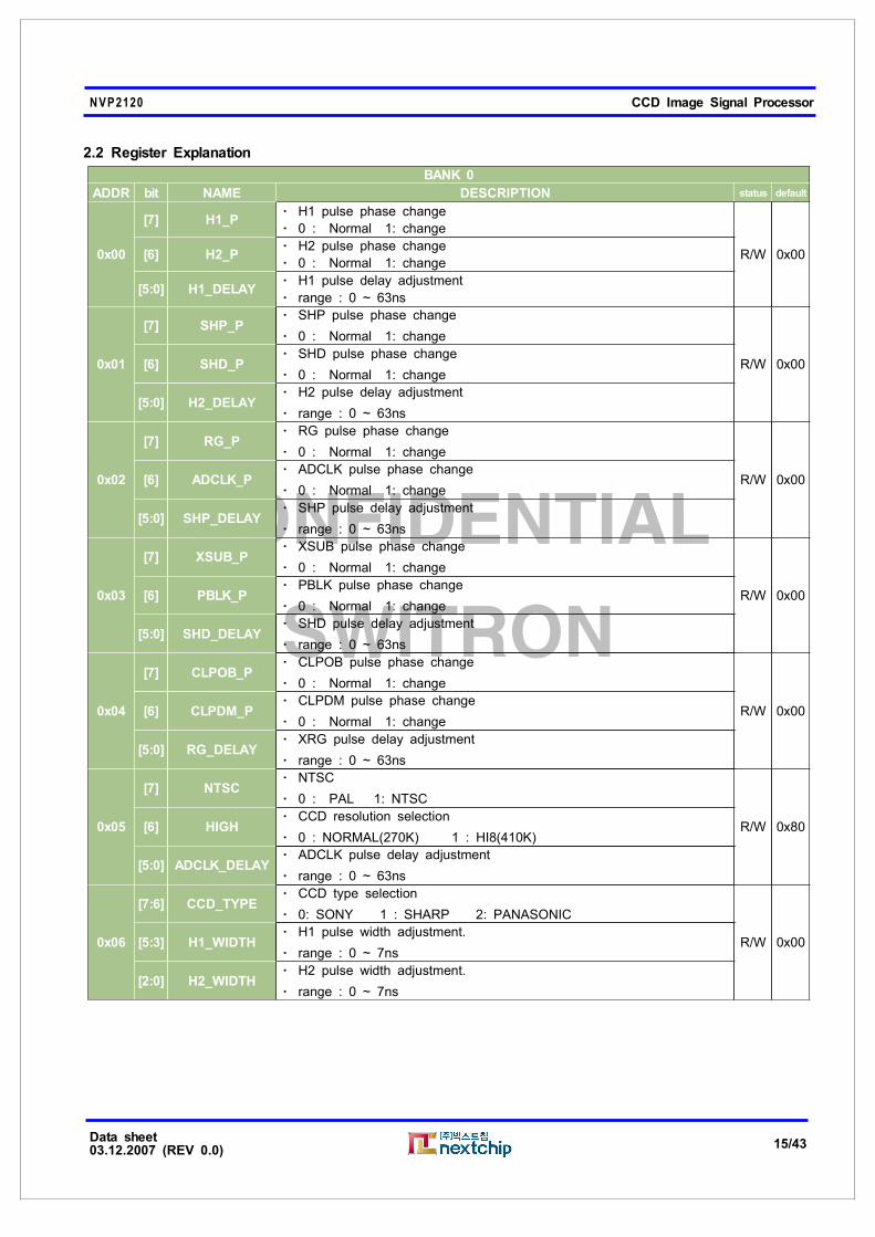
2.2 Register Explanation
BANK 0
ADDR bit NAME DESCRIPTION status default
0x00
[7] H1_PH1 pㆍ ulse phase change
0 : Normal 1: changeㆍ
R/W 0x00[6] H2_PH2 pㆍ ulse phase change
0 : Normal 1: changeㆍ
[5:0] H1_DELAYㆍ H1 pulse delay adjustment
range : 0 ~ 63nsㆍ
0x01
[7] SHP_PSHP pㆍ ulse phase change
0 : Normal 1: changeㆍ
R/W 0x00[6] SHD_PSHD pㆍ ulse phase change
0 : Normal 1: changeㆍ
[5:0] H2_DELAYH2ㆍ pulse delay adjustment
range : 0 ~ 63nsㆍ
0x02
[7] RG_PRG pㆍ ulse phase change
0 : Normal 1: changeㆍ
R/W 0x00[6] ADCLK_PADCLK pㆍ ulse phase change
0 : Normal 1: changeㆍ
[5:0] SHP_DELAYSHPㆍ pulse delay adjustment
range : 0 ~ 63nsㆍ
0x03
[7] XSUB_PXSUB pㆍ ulse phase change
0 : Normal 1: changeㆍ
R/W 0x00[6] PBLK_PPBLK pㆍ ulse phase change
0 : Normal 1: changeㆍ
[5:0] SHD_DELAYSHDㆍ pulse delay adjustment
range : 0 ~ 63nsㆍ
0x04
[7] CLPOB_PCLPOB pㆍ ulse phase change
0 : Normal 1: changeㆍ
R/W 0x00[6] CLPDM_PCLPDM pㆍ ulse phase change
0 : Normal 1: changeㆍ
[5:0] RG_DELAYXRGㆍ pulse delay adjustment
range : 0 ~ 63nsㆍ
0x05
[7] NTSCNTSCㆍ
0 : PAL 1: NTSCㆍ
R/W 0x80[6] HIGHCCD resolution selectionㆍ
0 : NORMAL(270K) 1 : HI8(410K)ㆍ
[5:0] ADCLK_DELAYADCLKㆍ pulse delay adjustment
range : 0 ~ 63nsㆍ
0x06
[7:6] CCD_TYPECCD type selectionㆍ
0: SONY 1 : SHARP 2: PANASONICㆍ
R/W 0x00[5:3] H1_WIDTHH1 pㆍ ulse width adjustment.
range : 0 ~ 7nsㆍ
[2:0] H2_WIDTHH2 pㆍ ulse width adjustment.
range : 0 ~ 7nsㆍ
CONFIDENTIAL
SWITRON
NVP2120 CCD Image Signal Processor
Data sheet03.12.2007 (REV 0.0)
16/43
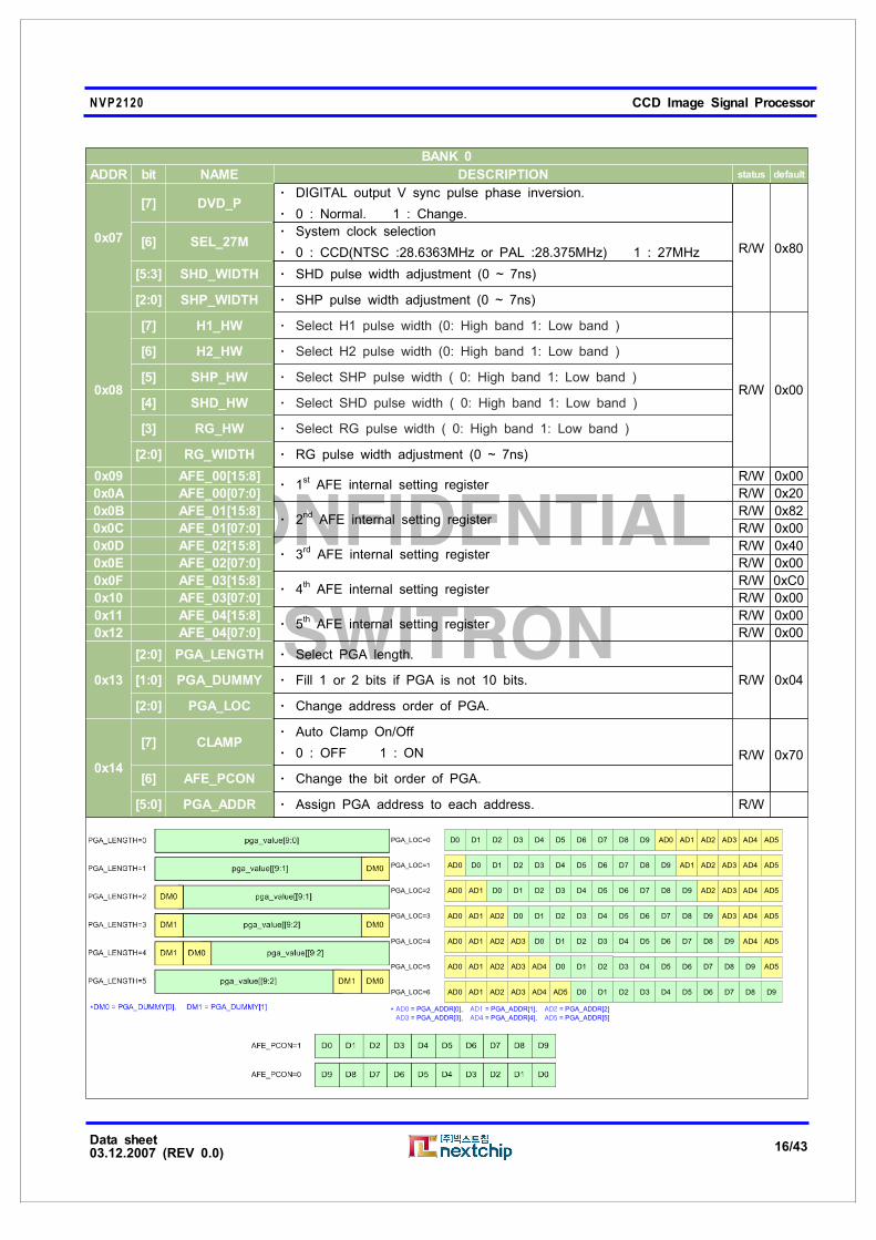
BANK 0
ADDR bit NAME DESCRIPTION status default
0x07
[7] DVD_PDIGITAL output V sync pulse phase inversion.ㆍ
0 : Normal. 1 : Change.ㆍ
R/W 0x80[6] SEL_27M
System clock selectionㆍ
0 : CCD(NTSC :28.6363MHz or PAL :28.375MHz) 1 : 27MHzㆍ
[5:3] SHD_WIDTH SHD pㆍ ulse width adjustment (0 ~ 7ns)
[2:0] SHP_WIDTH SHP pㆍ ulse width adjustment (0 ~ 7ns)
0x08
[7] H1_HW ㆍ Select H1 pulse width (0: High band 1: Low band )
R/W 0x00
[6] H2_HW ㆍ Select H2 pulse width (0: High band 1: Low band )
[5] SHP_HW ㆍ Select SHP pulse width ( 0: High band 1: Low band )
[4] SHD_HW ㆍ Select SHD pulse width ( 0: High band 1: Low band )
[3] RG_HW ㆍ Select RG pulse width ( 0: High band 1: Low band )
[2:0] RG_WIDTH RG pㆍ ulse width adjustment (0 ~ 7ns)
0x09 AFE_00[15:8]1ㆍ st
AFE internal setting registerR/W 0x00
0x0A AFE_00[07:0] R/W 0x20
0x0B AFE_01[15:8]2ㆍ nd
AFE internal setting registerR/W 0x82
0x0C AFE_01[07:0] R/W 0x00
0x0D AFE_02[15:8]3ㆍ rd
AFE internal setting registerR/W 0x40
0x0E AFE_02[07:0] R/W 0x00
0x0F AFE_03[15:8]4ㆍ th
AFE internal setting registerR/W 0xC0
0x10 AFE_03[07:0] R/W 0x00
0x11 AFE_04[15:8]5ㆍ th
AFE internal setting registerR/W 0x00
0x12 AFE_04[07:0] R/W 0x00
0x13
[2:0] PGA_LENGTH Select PGA length.ㆍ
R/W 0x04[1:0] PGA_DUMMY Fill 1 or 2 bits if PGA is not 10 bits.ㆍ
[2:0] PGA_LOC Change address order of PGA.ㆍ
0x14
[7] CLAMPAuto Clamp On/Offㆍ
0 : OFF 1 : ONㆍ R/W 0x70
[6] AFE_PCON Change the bit order of PGA.ㆍ
[5:0] PGA_ADDR Assign PGA address to each address.ㆍ R/W
D0 D1 D2 D3 D4 D5 D6 D7 D8 D9AD0 AD1 AD2 AD3 AD4 AD5
D0 D1 D2 D3 D4 D5 D6 D7 D8 D9
D0 D1 D2 D3 D4 D5 D6 D7 D8 D9
D0 D1 D2 D3 D4 D5 D6 D7 D8 D9
D0 D1 D2 D3 D4 D5 D6 D7 D8 D9
D0 D1 D2 D3 D4 D5 D6 D7 D8 D9
D0 D1 D2 D3 D4 D5 D6 D7 D8 D9 AD0 AD1 AD2 AD3 AD4 AD5PGA_LOC=0
PGA_LOC=1
PGA_LOC=2
PGA_LOC=3
PGA_LOC=4
PGA_LOC=5
PGA_LOC=6
AD2 AD3 AD4 AD5
AD3 AD4 AD5
AD4 AD5
AD5
AD0 AD1 AD2 AD3 AD4 AD5
AD0 AD1 AD2 AD3 AD4
AD0 AD1 AD2 AD3
AD0 AD1 AD2
AD0 AD1
* AD0 = PGA_ADDR[0], AD1 = PGA_ADDR[1], AD2 = PGA_ADDR[2]
AD3 = PGA_ADDR[3], AD4 = PGA_ADDR[4], AD5 = PGA_ADDR[5]
CONFIDENTIAL
SWITRON
NVP2120 CCD Image Signal Processor
Data sheet03.12.2007 (REV 0.0)
17/43
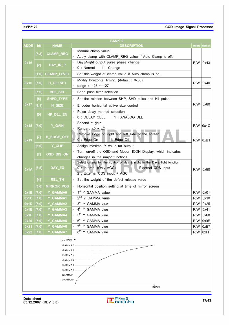
BANK 0
ADDR bit NAME DESCRIPTION status default
0x15
[7:3] CLAMP_REGManual clamp valueㆍ
Apply clamp with CLAMP_REG value if Auto Clamp is off.ㆍ
R/W 0x43[2] DAY_IR_P
Day&Night output pulse phase changeㆍ
0 : Normal 1 : Changeㆍ
[1:0] CLAMP_LEVEL Set the weight of clamp value if Auto clamp is on.ㆍ
0x16 [7:0] H_OFFSETModify horizontal timing. (default : 0x00)ㆍ
range : -128 ~ 127ㆍR/W 0x40
0x17
[7:6] BPF_SEL Band pass filter selectionㆍ
R/W 0x80
[5] SHPD_TYPE Set the relation between SHP, SHD pulse and H1 pulseㆍ
[4:1] H_SIZE Encoder horizontal active size controlㆍ
[0] HP_DLL_ENPulse delay method selectionㆍ
0 : DELAY CELL 1 : ANALOG DLLㆍ
0x18 [7:0] Y_GAINSecond Y gainㆍ
Range : x0 ~ x2ㆍR/W 0x4C
0x19[7] H_EDGE_OFF
Remove Edge on right and left side of the screen.ㆍ
0 : Edge On 1: Edge Offㆍ R/W 0xB1
[6:0] Y_CLIP Assign maximal Y value for outputㆍ
0x1A
[7] OSD_DIS_ONTurn on/off the OSD and Motion ICON Display, which indicatesㆍ
changes in the major functions
R/W 0x90[6:5] DAY_EX
ㆍ Select criteria for the control of day & night in the Day&Night function
0 : Internal (Only AGC) 1 : External CDS inputㆍ
2 : External CDS input + AGC
[4] REL_TH Set the weight of the defect release valueㆍ
[3:0] MIRROR_POS Horizontal position setting at time of mirror screenㆍ
0x1B [7:0] Y_GAMMA0 1ㆍ stY GAMMA value R/W 0x01
0x1C [7:0] Y_GAMMA1 2ㆍ ndY GAMMA vaue R/W 0x10
0x1D [7:0] Y_GAMMA2 3ㆍ rdY GAMMA vlue R/W 0x25
0x1E [7:0] Y_GAMMA3 4ㆍ thY GAMMA vlue R/W 0x41
0x1F [7:0] Y_GAMMA4 5ㆍ thY GAMMA vlue R/W 0x68
0x20 [7:0] Y_GAMMA5 6ㆍth
Y GAMMA vlue R/W 0x9E
0x21 [7:0] Y_GAMMA6 7ㆍth
Y GAMMA vlue R/W 0xE7
0x22 [7:0] Y_GAMMA7 8ㆍth
Y GAMMA vlue R/W 0xFF
GAMM A3
INPUT
OUTPUT
GAMM A0
GAMM A1
GAMM A2
GAMM A4
GAMM A5
GAMM A6
GAMM A7
CONFIDENTIAL
SWITRON
NVP2120 CCD Image Signal Processor
Data sheet03.12.2007 (REV 0.0)
18/43
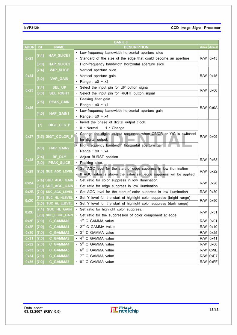
BANK 0
ADDR bit NAME DESCRIPTION status default
0x23[7:4] HAP_SLICE1
Low-frequency bandwidth horizontal aperture sliceㆍ
Standard of the size of the edge that could become an apertureㆍ R/W 0x45
[3:0] HAP_SLICE2 High-frequency bandwidth horizontal aperture sliceㆍ
0x24
[7:4] VAP_SLICE Vertical aperture sliceㆍ
R/W 0x45[3:0] VAP_GAIN
Vertical aperture gainㆍ
Range : x0 ~ x2ㆍ
0x25[7:4] SEL_UP Select the input pin for UP button signalㆍ
R/W 0x00[3:0] SEL_RIGHT Select the input pin for RIGHT button signalㆍ
0x26
[7:5] PEAK_GAINPeaking filter gainㆍ
Range : x0 ~ x4ㆍR/W 0x0A
[4:0] HAP_GAIN1Low-frequency bandwidth horizontal aperture gainㆍ
Range : x0 ~ x4ㆍ
0x27
[7] DIGT_CLK_PInvert the phase of digital output clock.ㆍ
0 : Normal 1 : Changeㆍ
R/W 0x09[6:5] DIGT_COLOR_PChange the digital output sequence when CB/CR or Y/C is switchedㆍ
for digital output.
[4:0] HAP_GAIN2High-frequency bandwidth horizontal aperture gainㆍ
Range : x0 ~ x4ㆍ
0x28[7:4] BF_DLY Adjust BURST positionㆍ
R/W 0x63[3:0] PEAK_SLICE Peaking slice.ㆍ
0x29 [7:0] SUE_AGC_LEVELSet AGC level for the start of edge suppress in low illuminationㆍ
If AGC value is above the value set, edge suppress will be applied.ㆍR/W 0x22
0x2A[7:4] SUC_AGC_GAIN Set ratio for color suppress in low illumination.ㆍ
R/W 0x28[3:0] SUE_AGC_GAIN Set ratio for edge suppress in low illumination.ㆍ
0x2B [7:0] SUC_AGC_LEVEL Set AGC level for the start of color suppress in low illuminationㆍ R/W 0x30
0x2C[7:4] SUC_HL_HLEVEL Set Y level for the start of highlight color suppress (bright range)ㆍ
R/W 0x90[3:0] SUC_HL_LLEVEL Set Y level for the start of highlight color suppress (dark range)ㆍ
0x2D[7:4] SUC_HL_GAIN Set ratio for highlight color suppress.ㆍ
R/W 0x31[3:0] SUC_EDGE_GAIN Set ratio for the suppression of color component at edge.ㆍ
0x2E [7:0] C_GAMMA0 1ㆍ stC GAMMA value R/W 0x01
0x2F [7:0] C_GAMMA1 2ㆍ ndC GAMMA value R/W 0x10
0x30 [7:0] C_GAMMA2 3ㆍ rdC GAMMA value R/W 0x25
0x31 [7:0] C_GAMMA3 4ㆍ thC GAMMA value R/W 0x41
0x32 [7:0] C_GAMMA4 5ㆍ thC GAMMA value R/W 0x68
0x33 [7:0] C_GAMMA5 6ㆍth
C GAMMA value R/W 0x9E
0x34 [7:0] C_GAMMA6 7ㆍth
C GAMMA value R/W 0xE7
0x35 [7:0] C_GAMMA7 8ㆍth
C GAMMA value R/W 0xFF
CONFIDENTIAL
SWITRON
NVP2120 CCD Image Signal Processor
Data sheet03.12.2007 (REV 0.0)
19/43
BANK 0
ADDR bit NAME DESCRIPTION status default
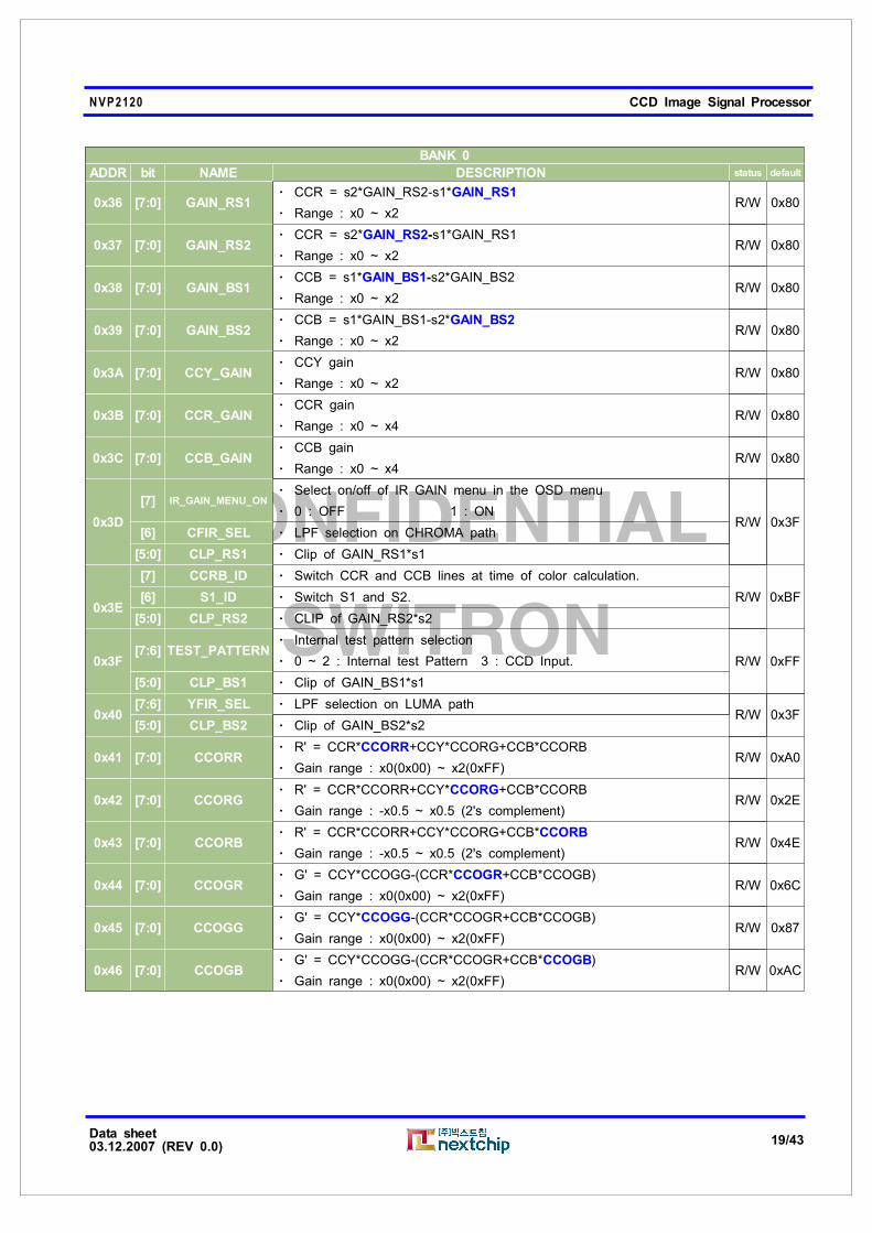
0x36 [7:0] GAIN_RS1CCR = s2*GAIN_RS2-s1*ㆍ GAIN_RS1
Range : x0 ~ x2ㆍR/W 0x80
0x37 [7:0] GAIN_RS2CCR = s2*ㆍ GAIN_RS2-s1*GAIN_RS1
Range : x0 ~ x2ㆍR/W 0x80
0x38 [7:0] GAIN_BS1CCB = s1*ㆍ GAIN_BS1-s2*GAIN_BS2
Range : x0 ~ x2ㆍR/W 0x80
0x39 [7:0] GAIN_BS2CCB = s1*GAIN_BS1-s2*ㆍ GAIN_BS2
Range : x0 ~ x2ㆍR/W 0x80
0x3A [7:0] CCY_GAINCCY gainㆍ
Range : x0 ~ x2ㆍR/W 0x80
0x3B [7:0] CCR_GAINCCR gainㆍ
Range : x0 ~ x4ㆍR/W 0x80
0x3C [7:0] CCB_GAINCCB gainㆍ
Range : x0 ~ x4ㆍR/W 0x80
0x3D
[7] IR_GAIN_MENU_ONSelect on/off of IR GAIN menu in the OSD menuㆍ
0 : OFF 1 : ONㆍR/W 0x3F
[6] CFIR_SEL LPF selection on CHROMA pathㆍ
[5:0] CLP_RS1 Clip of GAIN_RS1*s1ㆍ
0x3E
[7] CCRB_ID Switch CCR and CCB lines at time of color calculation.ㆍ
R/W 0xBF[6] S1_ID Switch S1 and S2.ㆍ
[5:0] CLP_RS2 CLIP of GAIN_RS2*s2ㆍ
0x3F[7:6] TEST_PATTERN
Internal test pattern selectionㆍ
0 ~ 2 : Internal test Pattern 3 : CCD Input.ㆍ R/W 0xFF
[5:0] CLP_BS1 Clip of GAIN_BS1*s1ㆍ
0x40[7:6] YFIR_SEL LPF selection on LUMA pathㆍ
R/W 0x3F[5:0] CLP_BS2 Clip of GAIN_BS2*s2ㆍ
0x41 [7:0] CCORRR' = CCR*ㆍ CCORR+CCY*CCORG+CCB*CCORB
Gain range : x0(0x00) ~ x2(0xFF)ㆍR/W 0xA0
0x42 [7:0] CCORGR' = CCR*CCORR+CCY*ㆍ CCORG+CCB*CCORB
Gain range : -x0.5 ~ x0.5 (2's complement)ㆍR/W 0x2E
0x43 [7:0] CCORBR' = CCR*CCORR+CCY*CCORG+CCB*ㆍ CCORB
Gain range : -x0.5 ~ x0.5 (2's complement)ㆍR/W 0x4E
0x44 [7:0] CCOGRG' = CCY*CCOGG-(CCR*ㆍ CCOGR+CCB*CCOGB)
Gain range : x0(0x00) ~ x2(0xFF)ㆍR/W 0x6C
0x45 [7:0] CCOGGG' = CCY*ㆍ CCOGG-(CCR*CCOGR+CCB*CCOGB)
Gain range : x0(0x00) ~ x2(0xFF)ㆍR/W 0x87
0x46 [7:0] CCOGBG' = CCY*CCOGG-(CCR*CCOGR+CCB*ㆍ CCOGB)
Gain range : x0(0x00) ~ x2(0xFF)ㆍR/W 0xAC

CONFIDENTIAL
SWITRON
NVP2120 CCD Image Signal Processor
Data sheet03.12.2007 (REV 0.0)
20/43
BANK 0
ADDR bit NAME DESCRIPTION status default
0x47 [7:0] CCOBRB' = CCR*ㆍ CCOBR+CCY*CCOBG+CCB*CCOBB
Gain range : -x0.5 ~ -x0.5 (2's complement)ㆍR/W 0xC6
0x48 [7:0] CCOBGB' = CCR*CCOBR+CCY*ㆍ CCOBG+CCB*CCOBB
Gain range : -x0.5 ~ -x0.5 (2's complement)ㆍR/W 0x52
0x49 [7:0] CCOBBB' = CCR*CCOBR+CCY*CCOBG+CCB*ㆍ CCOBB
Gain range : x0(0x00) ~ x2(0xFF)ㆍR/W 0xC4
0x4A [7:0] RWBRED gainㆍ
Gain range : x0(0x00) ~ x4(0xFF)ㆍR/W 0x5A
0x4B [7:0] GWBGREEN gainㆍ
Gain range : x0(0x00) ~ x2(0xFF)ㆍR/W 0x4A
0x4C [7:0] BWBBLUE gainㆍ
Gain range : x0(0x00) ~ x4(0xFF)ㆍR/W 0x51
0x4D [7:0] RBLKRED offsetㆍ
Gain range : -128 ~ 127 (2's complement)ㆍR/W 0x00
0x4E [7:0] GBLKGREEN offsetㆍ
Gain range : -128 ~ 127 (2's complement)ㆍR/W 0x00
0x4F [7:0] BBLKBLUE offsetㆍ
Gain range : -128 ~ 127 (2's complement)ㆍR/W 0x00
0x50 [7:0] CR_GAINCR GAINㆍ
Gain range : x0(0x00) ~ x2(0xFF)ㆍR/W 0x80
0x51 [7:0] CB_GAINCB GAINㆍ
Gain range : x0(0x00) ~ x2(0xFF)ㆍR/W 0x80
0x52 [7:0] HUE11ㆍ st
area HUE control
Data range : -45ㆍ ° ~ 45° (2's complement)R/W 0x00
0x53 [7:0] HUE22ㆍ
ndarea HUE control
Data range : -45ㆍ ° ~ 45° (2's complement)R/W 0x00
0x54 [7:0] HUE33ㆍ
rdarea HUE control
Data range : -45ㆍ ° ~ 45° (2's complement)R/W 0x00
0x55 [7:0] HUE44ㆍ
tharea HUE control
Data range : -45ㆍ ° ~ 45° (2's complement)R/W 0x00
0x56 [7:0] HUE55ㆍ
tharea HUE control
Data range : -45ㆍ ° ~ 45° (2's complement)R/W 0x00
0x57 [7:0] HUE66ㆍ
tharea HUE control
Data range : -45ㆍ ° ~ 45° (2's complement)R/W 0x00
0x58 [7:0] UV_GAIN11ㆍ
starea UV gain
Gain range : x0(0x00) ~ x2(0xFF)ㆍR/W 0x80
0x59 [7:0] UV_GAIN22ㆍ nd
area UV gain
Gain range : x0(0x00) ~ x2(0xFF)ㆍR/W 0x80

CONFIDENTIAL
SWITRON
NVP2120 CCD Image Signal Processor
Data sheet03.12.2007 (REV 0.0)
21/43
BANK 0
ADDR bit NAME DESCRIPTION status default
0x5A [7:0] UV_GAIN33ㆍ rd
area UV gain
Gain range : x0(0x00) ~ x2(0xFF)ㆍR/W 0x80
0x5B [7:0] UV_GAIN44ㆍ th
area UV gain
Gain range : x0(0x00) ~ x2(0xFF)ㆍR/W 0x80
0x5C [7:0] UV_GAIN55ㆍ th
area UV gain
Gain range : x0(0x00) ~ x2(0xFF)ㆍR/W 0x80
0x5D [7:0] UV_GAIN66ㆍ th
area UV gain
Gain range : x0(0x00) ~ x2(0xFF)ㆍR/W 0x80
E
Area 1
Area 2
Area 3
Area 4
Area 5
Area 6
0x5E
[7] BLCBLC(Back Light Compensation) On/Offㆍ
0 : OFF 1 : ONㆍ
R/W 0x95[6] BLC_AREA_VIEW
BLC AREA VIEW On/Offㆍ
0 : OFF 1 : ONㆍ
[5:0] BLC_GAIN Adjust ratio of screen brightness in the BLC areaㆍ
0x5F
[7:4] MOTION_AGC
Apply different motion threshold values for low illumination andㆍ
general conditions so that motion can be detected.
Set the criteria of low illumination for motion detection.ㆍ R/W 0x40
[3:0] MOTION_HIGHMotion detection is not to be performed when the screen is asㆍ
bright as it is set in the MOTION_HIGH or brighter
0x60 [7:0] AE_LEVEL Standard value for Auto Exposure when BLC is OFFㆍ R/W 0x54
0x61 [7:0] BLC_LEVEL Standard value for Auto Exposure when BLC is ONㆍ R/W 0x40
0x62 [7:0] MOTION_THL Low luminous motion threshold valueㆍ R/W 0x0F
0x63
[7] DAY_EXT_IN_PDay&Night external input pulse phase changeㆍ
0 : Normal 1 : Changeㆍ
R/W 0x48
[6:4] OSD_MDP Motion Icon display positionㆍ
[3] IRIS_LG_ONSelect the iris levelㆍ
0 : IRIS_LEVEL 1 : IRIS_LEVEL*gainㆍ
[2] IRIS_DAC_PORT Set DAC sleep mode register assignㆍ
[1] DAC_SL_MSEL
DAC sleep mode selectionㆍ
0 : DAC1_SL_REGㆍ
1 : DAC sleep when the LENS of the menu is set at manual
[0] MENU_LENS_DM
Set the submenu of LENS in the menu.ㆍ
0 : DC / Video / Manualㆍ
1 : DC / Manualㆍ
CONFIDENTIAL
SWITRON
NVP2120 CCD Image Signal Processor
Data sheet03.12.2007 (REV 0.0)
22/43
BANK 0
ADDR bit NAME DESCRIPTION status default
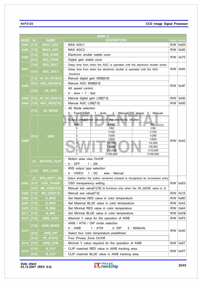
0x64 [7:0] MAX1_AGC MAX AGC1ㆍ R/W 0xD0
0x65 [7:0] MAX2_AGC MAX AGC2ㆍ R/W 0x00
0x66[7:4] ESS_ZONE Electronic shutter stable zoneㆍ
R/W 0x75[3:0] AED_ZONE Digital gain stable zoneㆍ
0x67
[7:4] ESS_SDLY ㆍ Delay time from when the AGC is operated until the electronic shutter works
R/W 0x00[3:0] AGC_SDLY
ㆍ Delay time from when the electronic shutter is operated until the AGC
functions
0x68
[7:6] AE_DG_REG[9:8] Manual digital gain MSB[9:8]ㆍ
R/W 0x4F[5:4] AGC_REG[9:8] Manual AGC MSB[9:0]ㆍ
[3:0] AE_SPDAE speed controlㆍ
0 : slow ~ 7 : fastㆍ
0x69 [7:0] AE_DG_REG[7:0] Manual digital gain LSB[7:0]ㆍ R/W 0x00
0x6A [7:0] AGC_REG[7:0] Manual AGC LSB[7:0]ㆍ R/W 0x00
0x6B
[7:6] AE_MODEAE Mode selectionㆍ
0 : Fixed(SSM) 1 : Auto 2 : Manual(256 steps) 3 : Manualㆍ
R/W 0x42
[5:3] SSM
Output predefined values of the electronic shutter.ㆍ
SSM NTSC PAL
0 1/60 1/50
1 1/100 1/120
2 1/250 1/250
3 1/500 1/500
4 1/2,000 1/2,000
5 1/5,000 1/5,000
6 1/10,000 1/10,000
7 1/100,000 1/100,000
[2] MOTION_TESTMotion area view On/Offㆍ
0 : OFF 1 : ONㆍ
[1:0] IRIS_LENSIRIS output type selectionㆍ
0 : VIDEO 1 : DC else : Manualㆍ
0x6C
[7] BTN_REPT_ON Select whether the button remained pressed is recognized as successive entryㆍ
R/W 0xE0[6:5] OSD_TRANS OSD transparency setting.ㆍ
[4:0] ME_ESS[12:8] Manual ess value[12:8]ㆍ (It functions only when the AE_MODE value is 3)
0x6D [7:0] ME_ESS[7:0] Manual ess value[7:0]ㆍ R/W 0x15
0x6E [7:0] R_MAX Set Maximal RED value in color temperatureㆍ R/W 0x8D
0x6F [7:0] B_MAX Set Maximal BLUE value in color temperatureㆍ R/W 0x43
0x70 [7:0] R_MIN Set Minimal RED value in color temperatureㆍ R/W 0x64
0x71 [7:0] B_MIN Set Minimal BLUE value in color temperatureㆍ R/W 0xCB
0x72 [7:0] AWB_HIGH Maximal Y value for the operation of AWBㆍ R/W 0xF0
0x73
[7:6] AWB_MODEAWB / ATW / DIP mode selectionㆍ
0 : AWBㆍ 1 : ATW 2: DIP 3 : MANUALR/W 0x40
[5:4] AWB_DIP Select four color temperature predefined.ㆍ
[3:0] PZ_STATE Four Privacy Zone On/Offㆍ
0x74 [7:0] AWB_LOW Minimal Y value required for the operation of AWBㆍ R/W 0x07
0x75[7:4] R_CLP CLIP maximal RED value in AWB tracking area.ㆍ
R/W 0xFF[3:0] B_CLP CLIP maximal BLUE value in AWB tracking area.ㆍ
CONFIDENTIAL
SWITRON
NVP2120 CCD Image Signal Processor
Data sheet03.12.2007 (REV 0.0)
23/43
BANK 0
ADDR bit NAME DESCRIPTION status default
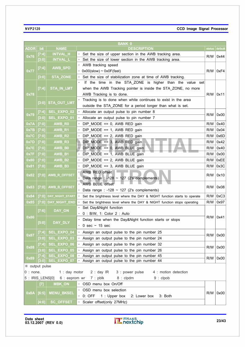
0x76[7:4] INTVAL_H Set the size of upper section in the AWB tracking area.ㆍ
R/W 0x44[3:0] INTVAL_L Set the size of lower section in the AWB tracking area.ㆍ
0x77[7:4] AWB_SPD
AWB tracking speedㆍ
0x00(slow) ~ 0x0F(fast)ㆍ R/W 0xF4
[3:0] STA_ZONE Set the size of stabilization zone at time of AWB tracking.ㆍ
0x78
[7:4] STA_IN_LMT
If the time in the STA_ZONE is higher than the value setㆍ
when the AWB Tracking pointer is inside the STA_ZONE, no more
AWB Tracking is to done. R/W 0x11
[3:0] STA_OUT_LMTTracking is to done when white continues to exist in the areaㆍ
outside the STA_ZONE for a period longer than what is set.
0x79[7:4] SEL_EXPO_02 Allocate an output pulse to pin number 8ㆍ
R/W 0x00[3:0] SEL_EXPO_01 Allocate an output pulse to pin number 7ㆍ
0x7A [7:0] AWB_R0 DIP_MODE == 0, AWB RED gainㆍ R/W 0x40
0x7B [7:0] AWB_R1 DIP_MODE == 1, AWB RED gainㆍ R/W 0x04
0x7C [7:0] AWB_R2 DIP_MODE == 2, AWB RED gainㆍ R/W 0x6D
0x7D [7:0] AWB_R3 DIP_MODE == 3, AWB RED gainㆍ R/W 0x42
0x7E [7:0] AWB_B0 DIP_MODE == 0, AWB BLUE gainㆍ R/W 0x40
0x7F [7:0] AWB_B1 DIP_MODE == 1, AWB BLUE gainㆍ R/W 0x00
0x80 [7:0] AWB_B2 DIP_MODE == 2, AWB BLUE gainㆍ R/W 0xEE
0x81 [7:0] AWB_B3 DIP_MODE == 3, AWB BLUE gainㆍ R/W 0x3C
0x82 [7:0] AWB_R_OFFSETAWB RED offsetㆍ
Data range : -128 ~ 127 (2's complements)ㆍR/W 0x10
0x83 [7:0] AWB_B_OFFSETAWB BLUE offsetㆍ
Data range : -128 ~ 127 (2's complements)ㆍR/W 0x08
0x84 [7:0] DAY_NIGHT_START ㆍ Set the brightness level where the DAY & NIGHT function starts to operate R/W 0xC3
0x85 [7:0] DAY_NIGHT_END ㆍ Set the brightness level where the DAY & NIGHT function stops operating R/W 0x97
0x86
[7:6] DAY_ONSet Day&Night functionㆍ
0 : B/W, 1: Color 2 : AutoㆍR/W 0x41
[5:0] DAY_DLYDelay time when the Day&Night function starts or stopsㆍ
0 sec ~ 15 secㆍ
0x87[7:4] SEL_EXPO_04 Assign an output pulse to the pin number 25ㆍ
R/W 0x00[3:0] SEL_EXPO_03 Assign an output pulse to the pin number 24ㆍ
0x88[7:4] SEL_EXPO_06 Assign an output pulse to the pin number 32ㆍ
R/W 0x00[3:0] SEL_EXPO_05 Assign an output pulse to the pin number 26ㆍ
0x89[7:4] SEL_EXPO_08 Assign an output pulse to the pin number 45ㆍ
R/W 0x00[3:0] SEL_EXPO_07 Assign an output pulse to the pin number 44ㆍ
output pulse※
0 : none. 1 : day motor 2 : day IR 3 : power pulse 4 : motion detection
5 : IRIS_LENS[0] 6 : eeprom wr 7 : pblk 8 : clpdm 9 : clpob
0x8A
[7] MBK_ON OSD menu box On/Offㆍ
R/W 0x00[6:5] MENU_BKSELOSD menu box selectionㆍ
0: OFF 1 : Upper box 2: Lower box 3: Bothㆍ
[4:0] SC_OFFSET Scaler offset(only 27MHz)ㆍ
CONFIDENTIAL
SWITRON
NVP2120 CCD Image Signal Processor
Data sheet03.12.2007 (REV 0.0)
24/43
BANK 0
ADDR bit NAME DESCRIPTION status default
0x8B
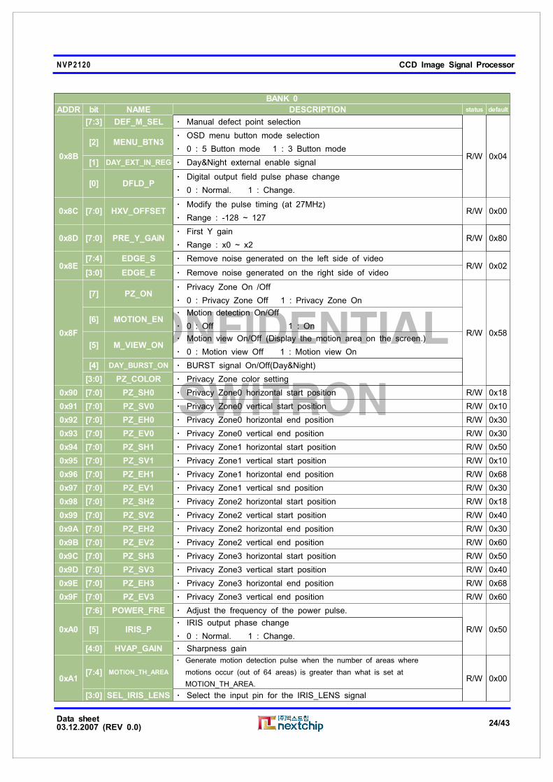
[7:3] DEF_M_SEL Manual defect point selectionㆍ
R/W 0x04
[2] MENU_BTN3OSD menu button mode selectionㆍ
0 : 5 Button mode 1 : 3 Button modeㆍ
[1] DAY_EXT_IN_REG Day&Night external enable signalㆍ
[0] DFLD_PDigital output field pulse phase changeㆍ
0 : Normal. 1 : Change.ㆍ
0x8C [7:0] HXV_OFFSETModify the pulse timing (at 27MHz)ㆍ
Range : -128 ~ 127ㆍR/W 0x00
0x8D [7:0] PRE_Y_GAiNFirst Y gainㆍ
Range : x0 ~ x2ㆍR/W 0x80
0x8E[7:4] EDGE_S Remove noise generated on the left side of videoㆍ
R/W 0x02[3:0] EDGE_E Remove noise generated on the right side of videoㆍ
0x8F
[7] PZ_ONPrivacy Zone On /Offㆍ
0 : Privacy Zone Off 1 : Privacy Zone Onㆍ
R/W 0x58
[6] MOTION_ENMotion detection On/Offㆍ
0 : Off 1 : Onㆍ
[5] M_VIEW_ONMotion view On/Off (Display the motion area on the screen.)ㆍ
0 : Motion view Off 1 : Motion view Onㆍ
[4] DAY_BURST_ON BURST signal On/Off(Day&Night)ㆍ
[3:0] PZ_COLOR Privacy Zone color settingㆍ
0x90 [7:0] PZ_SH0 Privacy Zone0 horizontal start positionㆍ R/W 0x18
0x91 [7:0] PZ_SV0 Privacy Zone0 vertical start positionㆍ R/W 0x10
0x92 [7:0] PZ_EH0 Privacy Zone0 horizontal end positionㆍ R/W 0x30
0x93 [7:0] PZ_EV0 Privacy Zone0 vertical end positionㆍ R/W 0x30
0x94 [7:0] PZ_SH1 Privacy Zone1 horizontal start positionㆍ R/W 0x50
0x95 [7:0] PZ_SV1 Privacy Zone1 vertical start positionㆍ R/W 0x10
0x96 [7:0] PZ_EH1 Privacy Zone1 horizontal end positionㆍ R/W 0x68
0x97 [7:0] PZ_EV1 Privacy Zone1 vertical snd positionㆍ R/W 0x30
0x98 [7:0] PZ_SH2 Privacy Zone2 horizontal start positionㆍ R/W 0x18
0x99 [7:0] PZ_SV2 Privacy Zone2 vertical start positionㆍ R/W 0x40
0x9A [7:0] PZ_EH2 Privacy Zone2 horizontal end positionㆍ R/W 0x30
0x9B [7:0] PZ_EV2 Privacy Zone2 vertical end positionㆍ R/W 0x60
0x9C [7:0] PZ_SH3 Privacy Zone3 horizontal start positionㆍ R/W 0x50
0x9D [7:0] PZ_SV3 Privacy Zone3 vertical start positionㆍ R/W 0x40
0x9E [7:0] PZ_EH3 Privacy Zone3 horizontal end positionㆍ R/W 0x68
0x9F [7:0] PZ_EV3 Privacy Zone3 vertical end positionㆍ R/W 0x60
0xA0
[7:6] POWER_FRE Adjust the frequency of the power pulse.ㆍ
R/W 0x50[5] IRIS_PIRIS output phase changeㆍ
0 : Normal. 1 : Change.ㆍ
[4:0] HVAP_GAIN Sharpness gainㆍ
0xA1[7:4] MOTION_TH_AREA
Generate motion detection pulse when the number of areas whereㆍ
motions occur (out of 64 areas) is greater than what is set at
MOTION_TH_AREA.R/W 0x00
[3:0] SEL_IRIS_LENS Select the input pin for the IRIS_LENS signalㆍ
CONFIDENTIAL
SWITRON
NVP2120 CCD Image Signal Processor
Data sheet03.12.2007 (REV 0.0)
25/43
BANK 0
ADDR bit NAME DESCRIPTION status default
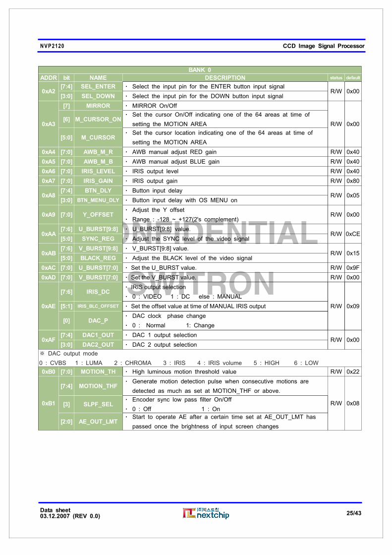
0xA2[7:4] SEL_ENTER Select the input pin for the ENTER button input signalㆍ
R/W 0x00[3:0] SEL_DOWN Select the input pin for the DOWN button input signalㆍ
0xA3
[7] MIRROR MIRROR On/Offㆍ
R/W 0x00[6] M_CURSOR_ON
Set the cursor On/Off indicating one of the 64 areas at time ofㆍ
setting the MOTION AREA
[5:0] M_CURSORSet the cursor location indicating one of the 64 areas at time ofㆍ
setting the MOTION AREA
0xA4 [7:0] AWB_M_R AWB manual adjust RED gainㆍ R/W 0x40
0xA5 [7:0] AWB_M_B AWB manual adjust BLUE gainㆍ R/W 0x40
0xA6 [7:0] IRIS_LEVEL IRIS output levelㆍ R/W 0x40
0xA7 [7:0] IRIS_GAIN IRIS output gainㆍ R/W 0x80
0xA8[7:4] BTN_DLY Button input delayㆍ
R/W 0x05[3:0] BTN_MENU_DLY Button input delay with OS MENU onㆍ
0xA9 [7:0] Y_OFFSETAdjust the Y offsetㆍ
Range : -128 ~ +127(2's complement)ㆍR/W 0x00
0xAA[7:6] U_BURST[9:8] ㆍ U_BURST[9:8] value.
R/W 0xCE[5:0] SYNC_REG Adjust the SYNC level of the video signalㆍ
0xAB[7:6] V_BURST[9:8] ㆍ V_BURST[9:8] value.
R/W 0x15[5:0] BLACK_REG Adjust the BLACK level of the video signalㆍ
0xAC [7:0] U_BURST[7:0] ㆍ Set the U_BURST value. R/W 0x9F
0xAD [7:0] V_BURST[7:0] ㆍ Set the V_BURST value. R/W 0x00
0xAE
[7:6] IRIS_DCㆍ IRIS output selection
0 : VIDEO 1 : DC else : MANUALㆍ
R/W 0x09[5:1] IRIS_BLC_OFFSET ㆍ Set the offset value at time of MANUAL IRIS output
[0] DAC_PDAC clock phase changeㆍ
0 : Normal 1: Changeㆍ
0xAF[7:4] DAC1_OUT DAC 1 output selectionㆍ
R/W 0x00[3:0] DAC2_OUT DAC 2 output selectionㆍ
DAC output mode※
0 : CVBS 1 : LUMA 2 : CHROMA 3 : IRIS 4 : IRIS volume 5 : HIGH 6 : LOW
0xB0 [7:0] MOTION_TH High luminous motion threshold valueㆍ R/W 0x22
0xB1
[7:4] MOTION_THFGenerate motion detection pulse when consecutive motions areㆍ
detected as much as set at MOTION_THF or above.
R/W 0x08[3] SLPF_SELEncoder sync low pass filter On/Offㆍ
0 : Off 1 : Onㆍ
[2:0] AE_OUT_LMTStart to operate AE after a certain time set at AE_OUT_LMT hasㆍ
passed once the brightness of input screen changes

CONFIDENTIAL
SWITRON
NVP2120 CCD Image Signal Processor
Data sheet03.12.2007 (REV 0.0)
26/43
BANK 0
ADDR bit NAME DESCRIPTION status default
0xB2 [7:0] MOTION_AREA[63:56]
Set the MOTION areaㆍ
R/W 0xFF
0xB3 [7:0] MOTION_AREA[55:48] R/W 0xFF
0xB4 [7:0] MOTION_AREA[47:40] R/W 0xFF
0xB5 [7:0] MOTION_AREA[39:32] R/W 0xFF
0xB6 [7:0] MOTION_AREA[31:24] R/W 0xFF
0xB7 [7:0] MOTION_AREA[23:16] R/W 0xFF
0xB8 [7:0] MOTION_AREA[15:8] R/W 0xFF
0xB9 [7:0] MOTION_AREA[7:0] R/W 0xFF
0xBA [7:0] BLC_AREA[63:56]
Set the BLC areaㆍ
R/W 0xFF
0xBB [7:0] BLC_AREA[55:48] R/W 0xFF
0xBC [7:0] BLC_AREA[47:40] R/W 0xFF
0xBD [7:0] BLC_AREA[39:32] R/W 0xFF
0xBE [7:0] BLC_AREA[31:24] R/W 0xFF
0xBF [7:0] BLC_AREA[23:16] R/W 0xFF
0xC0 [7:0] BLC_AREA[15:8] R/W 0xFF
0xC1 [7:0] BLC_AREA[7:0] R/W 0xFF

CONFIDENTIAL
SWITRON
NVP2120 CCD Image Signal Processor
Data sheet03.12.2007 (REV 0.0)
27/43
BANK 0
ADDR bit NAME DESCRIPTION status default
0xC2[7:4] SEL_DAY_EXT Select the input pin for the Day&Night external signalㆍ
R/W 0x00[3:0] SEL_MIRROR Select the input pin for the MIRROR control signalㆍ
0xC3[7:4] SEL_BLC Select the input pin for the BLC control signalㆍ
R/W 0x00[3:0] SEL_AGC Select the input pin for the AGC control signalㆍ
0xC4[7:4] SEL_AE1 Select the input pin for the AE_MODE[1] signalㆍ
R/W 0x00[3:0] SEL_AE0 Select the input pin for the AE_MODE[0] signalㆍ
0xC5[7:4] SEL_SSM1 Select the input pin for the SSM[1] signalㆍ
R/W 0x00[3:0] SEL_SSM0 Select the input pin for the SSM[0] signalㆍ
0xC6[7:4] SEL_LEFT Select the input pin for the LEFT button signalㆍ
R/W 0x00[3:0] SEL_SSM2 Select the input pin for the SSM[2] signalㆍ
selection input pin※
0x0 : not use 0x1 : #46 0x2 : #48 0x3 : #49 0x4 : #68 0x5 : #69 0x6 : #70 0x7 : #07
0x8 : #08 0x9 : #24 0xA : #25 0xB : #26 0xC : #32 0xD : #44 0xE : #45
0xC7[7:4] IRIS_GMAX Set the maximal value of IRIS_GAINㆍ
R/W 0x00[3:0] IRIS_GMIN Set the minimal value of IRIS_GAINㆍ
0xC8 [7:0] IR_GAIN[7:0] Set the INFRARED gain valueㆍ R/W 0x00
0xC9
[7] OSD_BLINKOSD blink function On/Offㆍ
0 : OFF 1 : ONㆍ
R/W 0x40
[6] OSD_SAVESave OSD. It is saved when the values are changed as follows:ㆍ
0->1, 1->0
[5] DHD_PDIGITAL output horizontal sync phase change.ㆍ
0 : Normal. 1 : Change.ㆍ
[4] OSD_DATA[8] Characters displayed OSDㆍ
[3:2] OSD_POS[9:8] Position of the characters to be displayed OSDㆍ
[1:0] OSD_CSEL Set the OSD font colorㆍ
0xCA [7:0] OSD_POS[7:0] Position of characters to be displayed OSDㆍ R/W 0x00
0xCB [7:0] OSD_DATA[7:0] Characters displayed OSDㆍ R/W 0x00
0xCC
[7] OSD_ONOSD On/Offㆍ
0 : Off 1 : Onㆍ
R/W 0x40[6] OSD_LPF_ON
OSD filter On/Offㆍ
0 : Off 1 : Onㆍ
[5] OSD_CLEAR Clear the OSD indication on the screenㆍ
[4:0] DEFT_STPOSCCD defect register with address (0~31) smaller than aㆍ
predetermined value is not replaced with the newly issued defect
0xCD[7:4] OSD_COLOR_01 OSD font color1ㆍ (Set the color for the items chosen in the OSD menu)
R/W 0xD3[3:0] OSD_COLOR_00 OSD font color2 (Set the basic font color in OSD menu)ㆍ
0xCE[7:4] OSD_COLOR_03 OSD font color3 (Set the OSD menu title & LOGO color)ㆍ
R/W 0x30[3:0] OSD_COLOR_02 OSD font color4 (Set the CAMERA ID color)ㆍ
0xCF[7:5] MENU_LANG OSD menu language selectionㆍ R/W 0x08
[4:0] GAMMA_SEL Select predefined GAMMA value (*OSD MENU)ㆍ R/W 0x00
0xD0[7:6] ID_REG12[1:0] 13ㆍ
thCAMERA ID character R/W 0x00
[5:0] ID_REG00[5:0] 1ㆍst
CAMERA ID character R/W 0x00
0xD1[7:6] ID_REG12[3:2] 13ㆍ
thCAMERA ID character R/W 0x00
[5:0] ID_REG01[5:0] 2ㆍ ndCAMERA ID character R/W 0x00

CONFIDENTIAL
SWITRON
NVP2120 CCD Image Signal Processor
Data sheet03.12.2007 (REV 0.0)
28/43
BANK 0
ADDR bit NAME DESCRIPTION status default
0xD2[7:6] ID_REG12[5:4] 13ㆍ th
CAMERA ID character R/W 0x00
[5:0] ID_REG02[5:0] 3ㆍ rdCAMERA ID character R/W 0x00
0xD3[7:6] ID_REG13[1:0] 14ㆍ th
CAMERA ID character R/W 0x00
[5:0] ID_REG03[5:0] 4ㆍ thCAMERA ID character R/W 0x00
0xD4[7:6] ID_REG13[3:2] 14ㆍ th
CAMERA ID characterR/W 0x00
[5:0] ID_REG04[5:0] 5ㆍ thCAMERA ID character
0xD5[7:6] ID_REG13[5:4] 14ㆍ
thCAMERA ID character
R/W 0x00[5:0] ID_REG05[5:0] 6ㆍ
thCAMERA ID character
0xD6[7:6] ID_REG14[1:0] 15ㆍ
thCAMERA ID character
R/W 0x00[5:0] ID_REG06[5:0] 7ㆍ
thCAMERA ID character
0xD7[7:6] ID_REG14[3:2] 15ㆍ
thCAMERA ID character
R/W 0x00[5:0] ID_REG07[5:0] 8ㆍ
thCAMERA ID character
0xD8[7:6] ID_REG14[5:4] 15ㆍ th
CAMERA ID characterR/W 0x00
[5:0] ID_REG08[5:0] 9ㆍ thCAMERA ID character
0xD9[7:6] ID_POS_Y[1:0] CAMERA ID vertical positionㆍ
R/W 0x00[5:0] ID_REG09[5:0] 10ㆍ th
CAMERA ID character
0xDA[7:6] ID_POS_Y[3:2] CAMERA ID vertical positionㆍ
R/W 0x00[5:0] ID_REG10[5:0] 11ㆍ th
CAMERA ID character
0xDB[7:6] ID_POS_X[1:0] CAMERA ID horizontal positionㆍ
R/W 0x00[5:0] ID_REG11[5:0] 12ㆍ
thCAMERA ID character
0xDC
[7] MAX_AGC_SELMAX_AGC selectionㆍ
0 : MAX1_AGC 1 : MAX2_AGCㆍ
R/W 0xD9
[6] OSD_ID_ONCAMERA ID On/Offㆍ
0 : OFF 1 : ONㆍ
[5:4] BLINK_TIMESet the blink timeㆍ
0 : 0.25s 1 : 0.5s 2 : 0.75s 3 : 1sㆍ
[3] ID_POS_Y[4] CAMERA ID vertical positionㆍ
[2:0] ID_POS_X[4:2] CAMERA ID horizontal positionㆍ
0xDD
[7] DAY_MOTOR_PDay&Night motor control pulse phase changeㆍ
0 : Normal 1: Changeㆍ
R/W 0x81[6:5] DAY_PULSE_SEL
Day&Night output pulse type selectionㆍ
Adjust the brightness of IRㆍ
0 : Maximum ~ 3 : Minimumㆍ
[4:0] POS_LEN OSD menu [LENS] item position(*OSD MENU)ㆍ
0xDE
[7] MENU_ICON_OFFMenu ICON On/Off(*OSD MENU)ㆍ
0 : On 1 : Offㆍ
R/W 0x62[6:5] MENU_OFF_TIME
OSD menu AUTO off term selectionㆍ
0 : 30 sec 1 : 1 min 2 : 2 min 3 : no offㆍ
[4:0] POS_SHT OSD menu [SHUTTER] item position(*OSD MENU)ㆍ
0xDF
[7] DIGT_OUTDigital output On/Offㆍ
0 : Off 1 : OnㆍR/W 0x03
[6:5] BLK_TH Black level horizontal aperture thresholdㆍ
[4:0] POS_BLC OSD menu [BLC] item position(*OSD MENU)ㆍ

CONFIDENTIAL
SWITRON
NVP2120 CCD Image Signal Processor
Data sheet03.12.2007 (REV 0.0)
29/43
BANK 0
ADDR bit NAME DESCRIPTION status default
0xE0
[7] NEGATIVE_IMGNegative image On/Offㆍ
0 : Off 1 : OnㆍR/W 0x04
[6:5] BLK_GAIN Black level horizontal aperture gainㆍ
[4:0] POS_AGC OSD menu [AGC] item position(*OSD MENU)ㆍ
0xE1
[7] HPF_SEL High frequence horizontal aperture filter selectionㆍ
R/W 0xE5[6:5] HAP_CLIP1 Low frequence horizontal aperture clipㆍ
[4:0] POS_WBL OSD menu [AWB] item position(*OSD MENU)ㆍ
0xE2
[7] OSD_OLENOSD outline On/Offㆍ
0 : Off 1 : OnㆍR/W 0x66
[6:5] VAP_CLIP Vertical aperture clipㆍ
[4:0] POS_FNC OSD menu [FUNCTION] item position(*OSD MENU)ㆍ
0xE3
[7] AWB_AE_DETECT
Set the point of starting AWBㆍ
0 : Start AWB irrespective of AEㆍ
1 : Start AWB once AE gets stabilized R/W 0x87
[6:5] AWB_METHOD1 AWB method1 selectionㆍ
[4:0] POS_ADJ OSD menu [ADJUST] item position(*OSD MENU)ㆍ
0xE4
[7] AWB_TR_CLIP
Clip more than what is set as R_MAX/R_MIN, B_MAX/B_MIN in theㆍ
AWB tracking area.
0 : Clip Off 1 : Clip Onㆍ R/W 0xF2
[6:5] AWB_METHOD2 AWB method2 selectionㆍ
[4:0] POS_LGG OSD menu [LANGUAGE] item position(*OSD MENU)ㆍ
0xE5
[7] AWB_METHOD3 AWB method3 selectionㆍ
R/W 0x4C[6:5] AE_GMAX AE digital gain maximum value selectionㆍ
[4:0] POS_CID OSD menu [CAMERA ID] item position(*OSD MENU)ㆍ
0xE6
[7] MENU_LOGO_OFFOSD menu LOGO On/Offㆍ
0 : On 1 : Offㆍ
R/W 0x2D[6] x Not availableㆍ
[5] HAP_SUP_SEL Horizontal edge suppress mode selectionㆍ
[4:0] POS_MIR OSD menu [MIRROR] item position(*OSD MENU)ㆍ
0xE7
[7] DYC_RANGEDigital output data range selectionㆍ
0 : 16 ~ 235 1: 1 ~ 254ㆍR/W 0xCE
[6:5] MENU_BKT Set menu box transparencyㆍ
[4:0] POS_DAY OSD menu [DAY&NIGHT] item position(*OSD MENU)ㆍ
0xE8
[7] AFE_DAC2_ON AFE DAC2 output On/Offㆍ
R/W 0x0F
[6] DEF_FA_ONField accumulation mode On/Off (defect search)ㆍ
0 : Off 1 : Onㆍ
[5] BTN_PButton press active Low or High selectionㆍ
0 : High 1 : Lowㆍ
[4:0] POS_MOT OSD menu [MOTION] item position(*OSD MENU)ㆍ
0xE9[7:5] DEF_FA_VALUE Field accumulation countㆍ
R/W 0x70[4:0] POS_PRI OSD menu [PRIVACY] item position(*OSD MENU)ㆍ
CONFIDENTIAL
SWITRON
NVP2120 CCD Image Signal Processor
Data sheet03.12.2007 (REV 0.0)
30/43
BANK 0
ADDR bit NAME DESCRIPTION status default
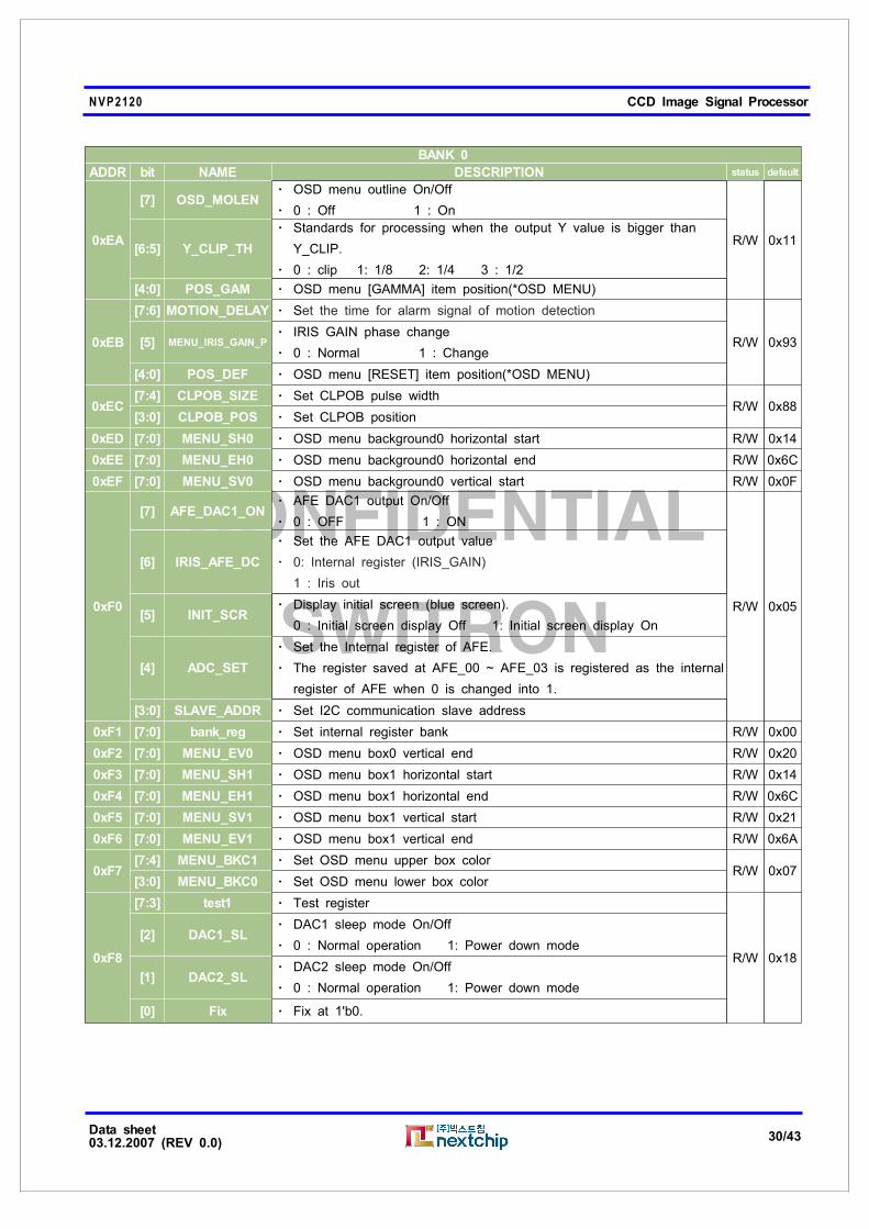
0xEA
[7] OSD_MOLENOSD menu outline On/Offㆍ
0 : Off 1 : Onㆍ
R/W 0x11[6:5] Y_CLIP_TH
Standards for processing when the output Y value is bigger thanㆍ
Y_CLIP.
0 : clip 1: 1/8 2: 1/4 3 : 1/2ㆍ
[4:0] POS_GAM OSD menu [GAMMA] item position(*OSD MENU)ㆍ
0xEB
[7:6] MOTION_DELAY Sㆍ et the time for alarm signal of motion detection
R/W 0x93[5] MENU_IRIS_GAIN_PIRIS GAIN phase changeㆍ
0 : Normal 1 : Changeㆍ
[4:0] POS_DEF OSD menu [RESET] item position(*OSD MENU)ㆍ
0xEC[7:4] CLPOB_SIZE Set CLPOB pulse widthㆍ
R/W 0x88[3:0] CLPOB_POS Set CLPOB positionㆍ
0xED [7:0] MENU_SH0 OSD menu background0 horizontal startㆍ R/W 0x14
0xEE [7:0] MENU_EH0 OSD menu background0 horizontal endㆍ R/W 0x6C
0xEF [7:0] MENU_SV0 OSD menu background0 vertical startㆍ R/W 0x0F
0xF0
[7] AFE_DAC1_ONAFE DAC1 output On/Offㆍ
0 : OFF 1 : ONㆍ
R/W 0x05
[6] IRIS_AFE_DC
Set the AFE DAC1 output valueㆍ
0: Internal register (IRIS_GAIN)ㆍ
1 : Iris out
[5] INIT_SCRDisplay initial screen (blue screen).ㆍ
0 : Initial screen display Off 1: Initial screen display On
[4] ADC_SET
Set the Internal register of AFE.ㆍ
The register saved at AFE_00 ~ AFE_03 is registered as the internalㆍ
register of AFE when 0 is changed into 1.
[3:0] SLAVE_ADDR Set I2C communication slave addressㆍ
0xF1 [7:0] bank_reg Set internal register bankㆍ R/W 0x00
0xF2 [7:0] MENU_EV0 OSD menu box0 vertical endㆍ R/W 0x20
0xF3 [7:0] MENU_SH1 OSD menu box1 horizontal startㆍ R/W 0x14
0xF4 [7:0] MENU_EH1 OSD menu box1 horizontal endㆍ R/W 0x6C
0xF5 [7:0] MENU_SV1 OSD menu box1 vertical startㆍ R/W 0x21
0xF6 [7:0] MENU_EV1 OSD menu box1 vertical endㆍ R/W 0x6A
0xF7[7:4] MENU_BKC1 Set OSD menu upper box colorㆍ
R/W 0x07[3:0] MENU_BKC0 Set OSD menu lower box colorㆍ
0xF8
[7:3] test1 Test registerㆍ
R/W 0x18
[2] DAC1_SLDAC1 sleep mode On/Offㆍ
0 : Normal operation 1: Power down modeㆍ
[1] DAC2_SLDAC2 sleep mode On/Offㆍ
0 : Normal operation 1: Power down modeㆍ
[0] Fix Fix at 1'b0.ㆍ

CONFIDENTIAL
SWITRON
NVP2120 CCD Image Signal Processor
Data sheet03.12.2007 (REV 0.0)
31/43
BANK 0
ADDR bit NAME DESCRIPTION status default
0xF9
[7:6] SD_H1Driving option selectionㆍ
0 : 12mA 1 : 14mA 2 : 16mA 3 : 18mAㆍ
R/W 0x00
[5] SL_H1Slew rate selectionㆍ
0 : Fast 1 : Slowㆍ
[4:3] SD_H2Driving option selectionㆍ
0 : 12mA 1 : 14mA 2 : 16mA 3 : 18mAㆍ
[2] Fix Fix at 1'b0.ㆍ
[1] SL_H2Slew rate selectionㆍ
0 : Fast 1 : Slowㆍ
[0] Fix Fix at 1'b0.ㆍ
0xFA
[7:6] SD_RGDriving option selectionㆍ
0 : 12mA 1 : 14mA 2 : 16mA 3 : 18mAㆍ
R/W 0x00[5] SL_RG
Slew rate selectionㆍ
0 : Fast 1 : Slowㆍ
[4:0] HAP_SUPPRESS Horizontal edge suppressㆍ
CONFIDENTIAL
SWITRON
NVP2120 CCD Image Signal Processor
Data sheet03.12.2007 (REV 0.0)
32/43
BANK 1
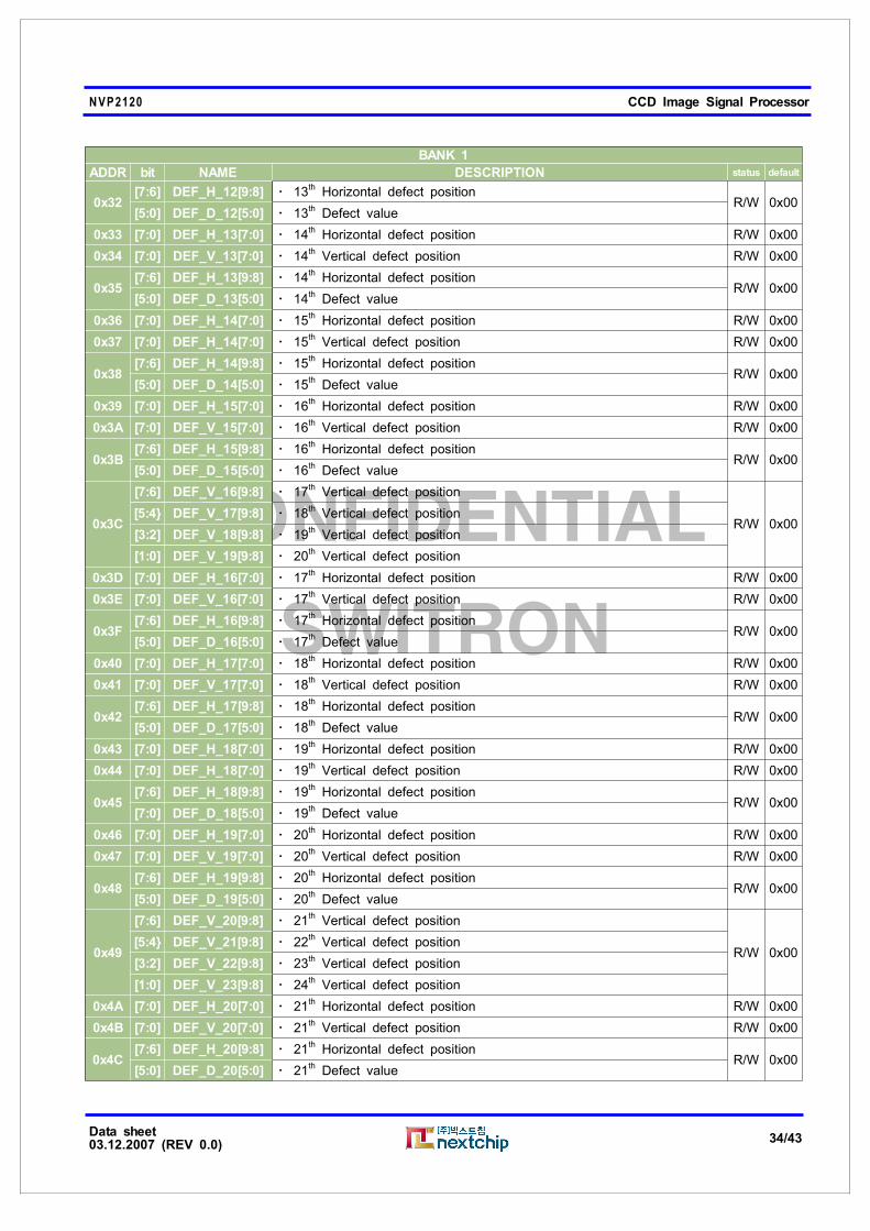
ADDR bit NAME DESCRIPTION status default
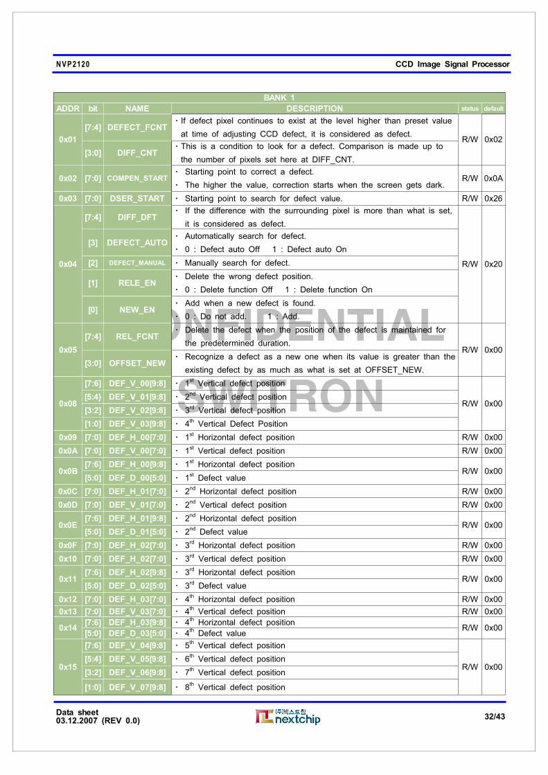
0x01
[7:4] DEFECT_FCNTIf defect pixel continues to exist at the level higher than preset valueㆍ
at time of adjusting CCD defect, it is considered as defect.R/W 0x02
[3:0] DIFF_CNTThis is a condition to look for a defect. Comparison is made up toㆍ
the number of pixels set here at DIFF_CNT.
0x02 [7:0] COMPEN_STARTStarting point to correct a defect.ㆍ
The higher the value, correction starts when the screen gets dark.ㆍR/W 0x0A
0x03 [7:0] DSER_START Starting point to search for defect value.ㆍ R/W 0x26
0x04
[7:4] DIFF_DFTIf the difference with the surrounding pixel is more than what is set,ㆍ
it is considered as defect.
R/W 0x20
[3] DEFECT_AUTOAutomatically search for defect.ㆍ
0 : Defect auto Off 1 : Defect auto Onㆍ
[2] DEFECT_MANUAL Manually search for defect.ㆍ
[1] RELE_ENDelete the wrong defect position.ㆍ
0 : Delete function Off 1 : Delete function Onㆍ
[0] NEW_ENAdd when a new defect is found.ㆍ
0 : Do not add. 1 : Add.ㆍ
0x05
[7:4] REL_FCNTDelete the defect when the position of the defect is maintained forㆍ
the predetermined duration.R/W 0x00
[3:0] OFFSET_NEWRecognize a defect as a new one when its value is greater than theㆍ
existing defect by as much as what is set at OFFSET_NEW.
0x08
[7:6] DEF_V_00[9:8] 1ㆍst
Vertical defect position
R/W 0x00[5:4} DEF_V_01[9:8] 2ㆍ nd
Vertical defect position
[3:2] DEF_V_02[9:8] 3ㆍ rdVertical defect position
[1:0] DEF_V_03[9:8] 4ㆍ thVertical Defect Position
0x09 [7:0] DEF_H_00[7:0] 1ㆍ stHorizontal defect position R/W 0x00
0x0A [7:0] DEF_V_00[7:0] 1ㆍ stVertical defect position R/W 0x00
0x0B[7:6] DEF_H_00[9:8] 1ㆍ st
Horizontal defect positionR/W 0x00
[5:0] DEF_D_00[5:0] 1ㆍst
Defect value
0x0C [7:0] DEF_H_01[7:0] 2ㆍnd
Horizontal defect position R/W 0x00
0x0D [7:0] DEF_V_01[7:0] 2ㆍnd
Vertical defect position R/W 0x00
0x0E[7:6] DEF_H_01[9:8] 2ㆍ
ndHorizontal defect position
R/W 0x00[5:0] DEF_D_01[5:0] 2ㆍ
ndDefect value
0x0F [7:0] DEF_H_02[7:0] 3ㆍrd
Horizontal defect position R/W 0x00
0x10 [7:0] DEF_H_02[7:0] 3ㆍ rdVertical defect position R/W 0x00
0x11[7:6] DEF_H_02[9:8] 3ㆍ rd
Horizontal defect positionR/W 0x00
[5:0] DEF_D_02[5:0] 3ㆍ rdDefect value
0x12 [7:0] DEF_H_03[7:0] 4ㆍ thHorizontal defect position R/W 0x00
0x13 [7:0] DEF_V_03[7:0] 4ㆍth
Vertical defect position R/W 0x00
0x14[7:6] DEF_H_03[9:8] 4ㆍ th
Horizontal defect positionR/W 0x00
[5:0] DEF_D_03[5:0] 4ㆍth
Defect value
0x15
[7:6] DEF_V_04[9:8] 5ㆍth
Vertical defect position
R/W 0x00[5:4] DEF_V_05[9:8] 6ㆍ
thVertical defect position
[3:2] DEF_V_06[9:8] 7ㆍ thVertical defect position
[1:0] DEF_V_07[9:8] 8ㆍth
Vertical defect position
CONFIDENTIAL
SWITRON
NVP2120 CCD Image Signal Processor
Data sheet03.12.2007 (REV 0.0)
33/43
BANK 1
ADDR bit NAME DESCRIPTION status default
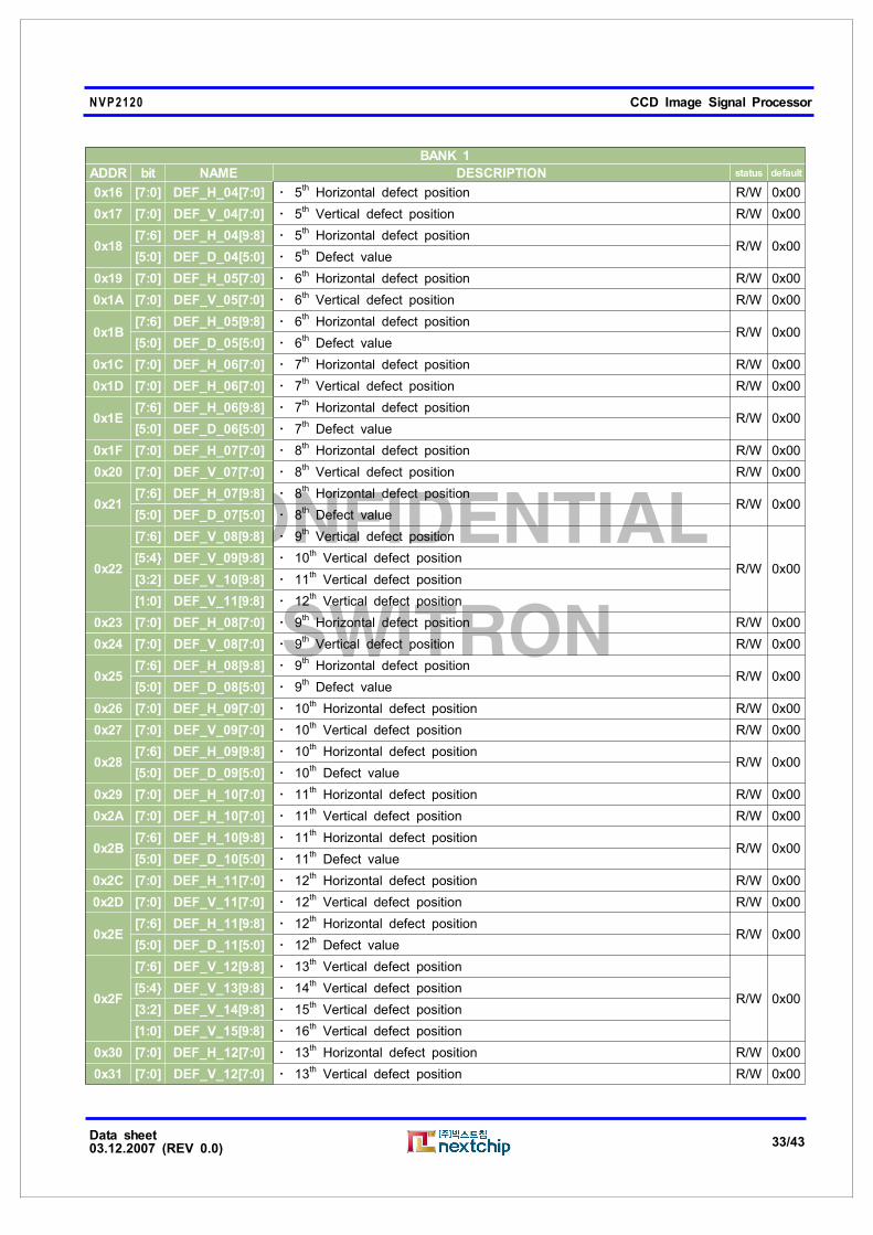
0x16 [7:0] DEF_H_04[7:0] 5ㆍ thHorizontal defect position R/W 0x00
0x17 [7:0] DEF_V_04[7:0] 5ㆍ thVertical defect position R/W 0x00
0x18[7:6] DEF_H_04[9:8] 5ㆍ th
Horizontal defect positionR/W 0x00
[5:0] DEF_D_04[5:0] 5ㆍ thDefect value
0x19 [7:0] DEF_H_05[7:0] 6ㆍ thHorizontal defect position R/W 0x00
0x1A [7:0] DEF_V_05[7:0] 6ㆍ thVertical defect position R/W 0x00
0x1B[7:6] DEF_H_05[9:8] 6ㆍ
thHorizontal defect position
R/W 0x00[5:0] DEF_D_05[5:0] 6ㆍ
thDefect value
0x1C [7:0] DEF_H_06[7:0] 7ㆍth
Horizontal defect position R/W 0x00
0x1D [7:0] DEF_H_06[7:0] 7ㆍth
Vertical defect position R/W 0x00
0x1E[7:6] DEF_H_06[9:8] 7ㆍ
thHorizontal defect position
R/W 0x00[5:0] DEF_D_06[5:0] 7ㆍ
thDefect value
0x1F [7:0] DEF_H_07[7:0] 8ㆍ thHorizontal defect position R/W 0x00
0x20 [7:0] DEF_V_07[7:0] 8ㆍ thVertical defect position R/W 0x00
0x21[7:6] DEF_H_07[9:8] 8ㆍ th
Horizontal defect positionR/W 0x00
[5:0] DEF_D_07[5:0] 8ㆍ thDefect value
0x22
[7:6] DEF_V_08[9:8] 9ㆍ thVertical defect position
R/W 0x00[5:4} DEF_V_09[9:8] 10ㆍ th
Vertical defect position
[3:2] DEF_V_10[9:8] 11ㆍth
Vertical defect position
[1:0] DEF_V_11[9:8] 12ㆍth
Vertical defect position
0x23 [7:0] DEF_H_08[7:0] 9ㆍth
Horizontal defect position R/W 0x00
0x24 [7:0] DEF_V_08[7:0] 9ㆍth
Vertical defect position R/W 0x00
0x25[7:6] DEF_H_08[9:8] 9ㆍ
thHorizontal defect position
R/W 0x00[5:0] DEF_D_08[5:0] 9ㆍ
thDefect value
0x26 [7:0] DEF_H_09[7:0] 10ㆍ thHorizontal defect position R/W 0x00
0x27 [7:0] DEF_V_09[7:0] 10ㆍ thVertical defect position R/W 0x00
0x28[7:6] DEF_H_09[9:8] 10ㆍ th
Horizontal defect positionR/W 0x00
[5:0] DEF_D_09[5:0] 10ㆍ thDefect value
0x29 [7:0] DEF_H_10[7:0] 11ㆍ thHorizontal defect position R/W 0x00
0x2A [7:0] DEF_H_10[7:0] 11ㆍ thVertical defect position R/W 0x00
0x2B[7:6] DEF_H_10[9:8] 11ㆍ
thHorizontal defect position
R/W 0x00[5:0] DEF_D_10[5:0] 11ㆍ
thDefect value
0x2C [7:0] DEF_H_11[7:0] 12ㆍth
Horizontal defect position R/W 0x00
0x2D [7:0] DEF_V_11[7:0] 12ㆍth
Vertical defect position R/W 0x00
0x2E[7:6] DEF_H_11[9:8] 12ㆍ
thHorizontal defect position
R/W 0x00[5:0] DEF_D_11[5:0] 12ㆍ
thDefect value
0x2F
[7:6] DEF_V_12[9:8] 13ㆍ thVertical defect position
R/W 0x00[5:4} DEF_V_13[9:8] 14ㆍ th
Vertical defect position
[3:2] DEF_V_14[9:8] 15ㆍ thVertical defect position
[1:0] DEF_V_15[9:8] 16ㆍ thVertical defect position
0x30 [7:0] DEF_H_12[7:0] 13ㆍ thHorizontal defect position R/W 0x00
0x31 [7:0] DEF_V_12[7:0] 13ㆍ thVertical defect position R/W 0x00
CONFIDENTIAL
SWITRON
NVP2120 CCD Image Signal Processor
Data sheet03.12.2007 (REV 0.0)
34/43
BANK 1
ADDR bit NAME DESCRIPTION status default
0x32[7:6] DEF_H_12[9:8] 13ㆍ th
Horizontal defect positionR/W 0x00
[5:0] DEF_D_12[5:0] 13ㆍ thDefect value
0x33 [7:0] DEF_H_13[7:0] 14ㆍ thHorizontal defect position R/W 0x00
0x34 [7:0] DEF_V_13[7:0] 14ㆍ thVertical defect position R/W 0x00
0x35[7:6] DEF_H_13[9:8] 14ㆍ th
Horizontal defect positionR/W 0x00
[5:0] DEF_D_13[5:0] 14ㆍ thDefect value
0x36 [7:0] DEF_H_14[7:0] 15ㆍth
Horizontal defect position R/W 0x00
0x37 [7:0] DEF_H_14[7:0] 15ㆍth
Vertical defect position R/W 0x00
0x38[7:6] DEF_H_14[9:8] 15ㆍ
thHorizontal defect position
R/W 0x00[5:0] DEF_D_14[5:0] 15ㆍ
thDefect value
0x39 [7:0] DEF_H_15[7:0] 16ㆍth
Horizontal defect position R/W 0x00
0x3A [7:0] DEF_V_15[7:0] 16ㆍth
Vertical defect position R/W 0x00
0x3B[7:6] DEF_H_15[9:8] 16ㆍ th
Horizontal defect positionR/W 0x00
[5:0] DEF_D_15[5:0] 16ㆍ thDefect value
0x3C
[7:6] DEF_V_16[9:8] 17ㆍ thVertical defect position
R/W 0x00[5:4} DEF_V_17[9:8] 18ㆍ th
Vertical defect position
[3:2] DEF_V_18[9:8] 19ㆍ thVertical defect position
[1:0] DEF_V_19[9:8] 20ㆍ thVertical defect position
0x3D [7:0] DEF_H_16[7:0] 17ㆍth
Horizontal defect position R/W 0x00
0x3E [7:0] DEF_V_16[7:0] 17ㆍth
Vertical defect position R/W 0x00
0x3F[7:6] DEF_H_16[9:8] 17ㆍ
thHorizontal defect position
R/W 0x00[5:0] DEF_D_16[5:0] 17ㆍ
thDefect value
0x40 [7:0] DEF_H_17[7:0] 18ㆍth
Horizontal defect position R/W 0x00
0x41 [7:0] DEF_V_17[7:0] 18ㆍth
Vertical defect position R/W 0x00
0x42[7:6] DEF_H_17[9:8] 18ㆍ th
Horizontal defect positionR/W 0x00
[5:0] DEF_D_17[5:0] 18ㆍ thDefect value
0x43 [7:0] DEF_H_18[7:0] 19ㆍ thHorizontal defect position R/W 0x00
0x44 [7:0] DEF_H_18[7:0] 19ㆍ thVertical defect position R/W 0x00
0x45[7:6] DEF_H_18[9:8] 19ㆍ th
Horizontal defect positionR/W 0x00
[7:0] DEF_D_18[5:0] 19ㆍ thDefect value
0x46 [7:0] DEF_H_19[7:0] 20ㆍth
Horizontal defect position R/W 0x00
0x47 [7:0] DEF_V_19[7:0] 20ㆍth
Vertical defect position R/W 0x00
0x48[7:6] DEF_H_19[9:8] 20ㆍ
thHorizontal defect position
R/W 0x00[5:0] DEF_D_19[5:0] 20ㆍ
thDefect value
0x49
[7:6] DEF_V_20[9:8] 21ㆍth
Vertical defect position
R/W 0x00[5:4} DEF_V_21[9:8] 22ㆍ
thVertical defect position
[3:2] DEF_V_22[9:8] 23ㆍ thVertical defect position
[1:0] DEF_V_23[9:8] 24ㆍ thVertical defect position
0x4A [7:0] DEF_H_20[7:0] 21ㆍ thHorizontal defect position R/W 0x00
0x4B [7:0] DEF_V_20[7:0] 21ㆍ thVertical defect position R/W 0x00
0x4C[7:6] DEF_H_20[9:8] 21ㆍ th
Horizontal defect positionR/W 0x00
[5:0] DEF_D_20[5:0] 21ㆍ thDefect value
CONFIDENTIAL
SWITRON
NVP2120 CCD Image Signal Processor
Data sheet03.12.2007 (REV 0.0)
35/43
BANK 1
ADDR bit NAME DESCRIPTION status default
0x4D [7:0] DEF_H_21[7:0] 22ㆍ thHorizontal defect position R/W 0x00
0x4E [7:0] DEF_V_21[7:0] 22ㆍ thVertical defect position R/W 0x00
0x4F[7:6] DEF_H_21[9:8] 22ㆍ th
Horizontal defect positionR/W 0x00
[5:0] DEF_D_21[5:0] 22ㆍ thDefect value
0x50 [7:0] DEF_H_22[7:0] 23ㆍ thHorizontal defect position R/W 0x00
0x51 [7:0] DEF_H_22[7:0] 23ㆍ thVertical defect position R/W 0x00
0x52[7:6] DEF_H_22[9:8] 23ㆍ
thHorizontal defect position
R/W 0x00[5:0] DEF_D_22[5:0] 23ㆍ
thDefect value
0x53 [7:0] DEF_H_23[7:0] 24ㆍth
Horizontal defect position R/W 0x00
0x54 [7:0] DEF_V_23[7:0] 24ㆍth
Vertical defect position R/W 0x00
0x55[7:6] DEF_H_23[9:8] 24ㆍ
thHorizontal defect position
R/W 0x00[7:0] DEF_D_23[5:0] 24ㆍ
thDefect value
0x56
[7:6] DEF_V_24[9:8] 25ㆍ thVertical defect position
R/W 0x00[5:4] DEF_V_25[9:8] 26ㆍ th
Vertical defect position
[3:2] DEF_V_26[9:8] 27ㆍ thVertical defect position
[1:0] DEF_V_27[9:8] 28ㆍ thVertical defect position
0x57 [7:0] DEF_H_24[7:0] 25ㆍ thHorizontal defect position R/W 0x00
0x58 [7:0] DEF_V_24[7:0] 25ㆍ thVertical defect position R/W 0x00
0x59[7:6] DEF_H_24[9:8] 25ㆍ
thHorizontal defect position
R/W 0x00[5:0] DEF_D_24[5:0] 25ㆍ
thDefect value
0x5A [7:0] DEF_H_25[7:0] 26ㆍth
Horizontal defect position R/W 0x00
0x5B [7:0] DEF_V_25[7:0] 26ㆍth
Vertical defect position R/W 0x00
0x5C[7:6] DEF_H_25[9:8] 26ㆍ
thHorizontal defect position
R/W 0x00[5:0] DEF_D_25[5:0] 26ㆍ
thDefect value
0x5D [7:0] DEF_H_26[7:0] 27ㆍ thHorizontal defect position R/W 0x00
0x5E [7:0] DEF_H_26[7:0] 27ㆍ thVertical defect position R/W 0x00
0x5F[7:6] DEF_H_26[9:8] 27ㆍ th
Horizontal defect positionR/W 0x00
[5:0] DEF_D_26[5:0] 27ㆍ thDefect value
0x60 [7:0] DEF_H_27[7:0] 28ㆍ thHorizontal defect position R/W 0x00
0x61 [7:0] DEF_V_27[7:0] 28ㆍ thVertical defect position R/W 0x00
0x62[7:6] DEF_H_27[9:8] 28ㆍ
thHorizontal defect position
R/W 0x00[5:0] DEF_D_27[5:0] 28ㆍ
thDefect value
0x63
[7:6] DEF_V_28[9:8] 29ㆍth
Vertical defect position
R/W 0x00[5:4} DEF_V_29[9:8] 30ㆍ
thVertical defect position
[3:2] DEF_V_30[9:8] 31ㆍth
Vertical defect position
[1:0] DEF_V_31[9:8] 32ㆍth
Vertical defect position
0x64 [7:0] DEF_H_28[7:0] 29ㆍ thHorizontal defect position R/W 0x00
0x65 [7:0] DEF_V_28[7:0] 29ㆍ thVertical defect position R/W 0x00
0x66[7:6] DEF_H_28[9:8] 29ㆍ th
Horizontal defect positionR/W 0x00
[5:0] DEF_D_28[5:0] 29ㆍ thDefect value
0x67 [7:0] DEF_H_29[7:0] 30ㆍ thHorizontal defect position R/W 0x00
0x68 [7:0] DEF_V_29[7:0] 30ㆍ thVertical defect position R/W 0x00

CONFIDENTIAL
SWITRON
NVP2120 CCD Image Signal Processor
Data sheet03.12.2007 (REV 0.0)
36/43
BANK 1
ADDR bit NAME DESCRIPTION status default
0x69[7:6] DEF_H_29[9:8] 30ㆍ th
Horizontal defect positionR/W 0x00
[5:0] DEF_D_29[5:0] 30ㆍ thDefect value
0x6A [7:0] DEF_H_30[7:0] 31ㆍ thHorizontal defect position R/W 0x00
0x6B [7:0] DEF_H_30[7:0] 31ㆍ thVertical defect position R/W 0x00
0x6C[7:6] DEF_H_30[9:8] 31ㆍ th
Horizontal defect positionR/W 0x00
[5:0] DEF_D_30[5:0] 31ㆍ thDefect value
0x6D [7:0] DEF_H_31[7:0] 32ㆍth
Horizontal defect position R/W 0x00
0x6E [7:0] DEF_V_31[7:0] 32ㆍth
Vertical defect position R/W 0x00
0x6F[7:6] DEF_H_31[9:8] 32ㆍ
thHorizontal defect position
R/W 0x00[5:0] DEF_D_31[5:0] 32ㆍ
thDefect value
0x70
[7] AED_SPDAE digital gain speed selectionㆍ
0 : Normal 1 : FastㆍR/W 0x35
[6:4] V_OFFSET Encoder vertical direction offsetㆍ
[3:0] OSD_ROMRAM_POS Set delay for timing on font displayㆍ
0x71[7:4] SEL_IRISL Select the input pin for the IRIS control left button signalㆍ
R/W 0x00[3:0] SEL_IRISR Select the input pin for the IRIS control right button signalㆍ
0x72[7:4] Fix Fix at 1'b0.ㆍ
R/W 0x00[3:0] SEL_MOTION Select the input pin for the MOTION enable signalㆍ
CONFIDENTIAL
SWITRON
NVP2120 CCD Image Signal Processor
Data sheet03.12.2007 (REV 0.0)
37/43
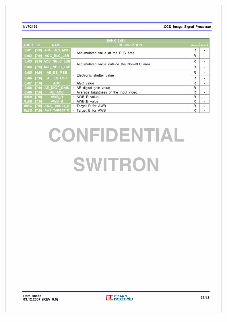
BANK 0x81
ADDR bit NAME DESCRIPTION status default
0x81 [5:0] ACC_BLC_MSBAccumulated value at the BLC areaㆍ
R -
0x82 [7:0] ACC_BLC_LSB R -
0x83 [5:0] ACC_NBLC_LSBAccumulated value outside the Non-BLC areaㆍ
R -
0x84 [7:0] ACC_NBLC_LSB R -
0x85 [4:0] AE_ES_MSBElectronic shutter valueㆍ
R -
0x86 [7:0] AE_ES_LSB R -
0x87 [7:0] AGC AGC valueㆍ R -
0x88 [7:0] AE_DIGT_GAIN AE digital gain valueㆍ R -
0x89 [7:0] AE_ACC Average brightness of the input videoㆍ R -
0x8A [7:0] AWB_R AWB R valueㆍ R -
0x8B [7:0] AWB_B AWB B valueㆍ R -
0x8C [7:0] AWB_TARGET_R Target R for AWBㆍ R -
0x8D [7:0] AWB_TARGET_B Target B for AWBㆍ R -
CONFIDENTIAL
SWITRON
NVP2120 CCD Image Signal Processor
Data sheet03.12.2007 (REV 0.0)
38/43
3. Electrical Characteristics
3.1. Absolute Maximum Ratings
3.2. Recommended Operating Condition
3.3. DC Characteristics
*Note2 : 3.3V data pins
expect 5V data pins
*Note3 : 5V data pins
XRG, H1, H2 pins(#5, #4, #3)
Parameter Min Max Unit
Power supply voltage -0.5 6 V
Voltage on any 3.3V input pin 3.0 3.6 V
Voltage on any 5V input pin 4.5 5.5 V
Storage temperature -40 125 ℃
Parameter Symbol Min Typ Max Unit
3.3V Digital power supply voltage VDD3 3.0 3.3 3.6 V
3.3V Analog power supply voltage AVDD3 3.0 3.3 3.6 V
5.0V Digital power supply voltage VDD5 4.5 5.0 5.5 V
Commercial temperature range TA 0 - 70 ℃
Industrial temperature range TA -40 - 85 ℃
Parameter Symbol Min Typ Max Unit
3.3V Pins *Note1
Input low voltage VIL3 VSS-0.3 - 0.3VDD3 V
Input high voltage VIH3 0.7VDD3 - VDD3+0.3 V
Input low current (VIN3 = VSS) IIL3 - - -10 uA
Input high current (VIN3 = VDD3) IIH3 - - 10 uA
Input capacitance (f = 1Mhz, VIN3= 2.4V) CIN - - 10 pF
Output low voltage (IOH3 = 3.2mA) VOL3 - - 0.4 V
Output high voltage (IOH3 = -400uA) VOH3 2.4 - VDD3 V
Output capacitance COUT - - 10 pF
5.0V Pins *Note2
Input low voltage VIL5 VSS-0.5 - 0.8 V
Input high voltage VIH5 2.0 - VDD5+0.5 V
Input low current (VIN5 = VSS) IIL5 - - -10 uA
Input high current (VIN5 = VDD5) IIH5 - - 10 uA
Input capacitance (f = 1Mhz, VIN5 = 2.4V) CIN - - 10 pF
Output low voltage (IOH5 = 3.2mA) VOL5 - - 0.4 V
Output high voltage (IOH5 = -400uA) VOH5 2.4 - VDD5 V
Output capacitance COUT - - 10 pF

CONFIDENTIAL
SWITRON
NVP2120 CCD Image Signal Processor
Data sheet03.12.2007 (REV 0.0)
39/43
4. System Application
4.1.1 Circuit Guide (NVP2120)
XSUB DIG_CLK
TC6T22/6.3V(A)
1 2
C150.1u(F)
D1
SC
K
XSG2
C201u(F)
+ TC14T22/6.3V(A)
12
XSG1
+3.3_VDD3
EXP_I_3
D3KDS160E
12
L2
10uH
U5AT24C16N (SOP)
12345 6 7 8
AO
0A
O1
AO
2G
ND
SD
AS
CL
WP
VC
C
L3
10uH
D0
R2
0
R164.7K
DIG_5
+3.3V
EXP_IO_2
+TC2
T10/10V(A)
12
DIG
_1
EX
P_IO
_6
IRIS_SIGNAL
D8
R7200
D2
L4
10uH
SL
U1
NJM2575F1
1
2
34
5
6P/S
VOUT
VSAGVIN
GND
VCC
+
TC9T22/6.3V(A)
12
SD
AT
A
C2620p(B)
DIG
_3
D3
D5
U4KIA7029AT(TSM)
2
3
1
RE
SE
T
GN
D
VC
C
R154.7K
C5
NC
SHP
R14150
SCL
R8100K
NTSC:28.63636MHZ
R6 4.7K
EX
P_I_
6
SDA
+
TC13T22/6.3V(A)
12
+5.0V
C40.1u(F)
+
TC10T22/6.3V(A)
12
EXP_IO_1
R3
75
R41K
D6
C7 0.1u(F)
EX
P_I_
4
V1
R1
NC
PAL:28.375MHZ
C17 0.1u(F)
+3.3V
D7
C130.1u(F)
EX
P_I_
5
C10.1u(F)
XRGH1
R5 2K
C25NC
T120pF
D4
EXP_I_1
+
TC5T22/6.3V(A)
12
+3.3V
V3
L8
10uH
C9 0.1u(F)
EX
P_IO
_5
V4
ADCLK
C140.1u(F)
SHD
+3.3V
C8 0.1u(B)
C100.1u(F)
TC4T100/6.3V(B2)1 2
+ TC3T22/6.3V(A)
12
DIG
_0
H2
CN4
4P_1.25mm
1234
DIG
_2
EXP_I_2
EX
P_IO
_4
L1
10uH
C220.1u(F)
+3.3V
EX
P_IO
_3
V2
+ TC1T22/6.3V(A)
12
+3.3V
R13
1M
C20.1u(F)
D9
DIG_6
+3.3V
U2NVP2120
98765432
18
16151413121110
21
22
23
24
25
26
27
28
29
30
31
32
33
34
1
17
1920
35
36
37
39
40
38
41424344
4647484950515253545556
5960
61
62
63
64
65
66
67
68
71
72
73
74
77
45
69
70
75
5758
76
78
79
80
BGR(NC)EXP_IO_2EXP_IO_1VSSXRGH1H2VDD5
V3
V1V2XSUBVDDIVSSVDD3VDD3
AF
E_S
CL
AF
E_S
DA
AF
E_S
LD
EX
P_IO
_3
EX
P_IO
_4
EX
P_IO
_5
VD
D3
XT
ALI
XT
ALO
VS
SV
SS
EX
P_IO
_6
I2C
_S
CL
I2C
_S
DA
VSS
XSG1
XSG2V4
DIG
T_[0
]
DIG
T_[1
]D
IGT
_[2
]
TS
TO
VD
D3
DIG
T_[3
]
VSSDIGT_[4]DIGT_[5]
DIGT[6]_EXP_IO_7
EXP_I_1DIGT_CLK
EXP_I_2EXP_I_3
RSTBVDDIVDD3DAC1
AVDD3YVSSADAC2
COMPIREF
VR
EF
VS
SU
B
CF
AIN
[9]
CF
AIN
[8]
CF
AIN
[7]
CF
AIN
[6]
CF
AIN
[5]
EX
P_I_
4
CF
AIN
[4]
CF
AIN
[3]
CF
AIN
[2]
CF
AIN
[1]
AD
CLK
DIGT[7]_EXP_IO_8
EX
P_I_
5
EX
P_I_
6
CF
AIN
[0]
AVDD3CVSSA
VS
S
VD
D3
SH
PS
HD
C230.1u(F)
C30.1u(F)
VIDEO
DIG_4
L7
10uH
C11 0.1u(F)
DIG_7
X1
Circuit Guide
Ref. Desg. Value Maker Stanrd Type (Size)
L1~L8 10uH TDKNLFV25T-100K-PF 2520
NLCV32T-100K-PF 3225
TC1~8 22/6.3VPartsnic TLMOJ226ASSR 3216
SAMSUNG TCSCSOJ226MA 3216
C1~C23 0.1uF SAMSUNG CL10F104ZB8 1608
R1~R23 10K ~ SAMSUNG RC1608J103CS 1608
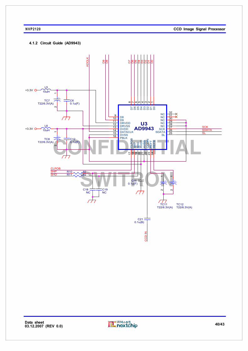
CONFIDENTIAL
SWITRON
NVP2120 CCD Image Signal Processor
Data sheet03.12.2007 (REV 0.0)
40/43
4.1.2 Circuit Guide (AD9943)
CC
D IN
C120.1u(F)
C210.1u(B)
+3.3V
D6
U3AD9943
12345678
910111213141516
17
18
19
20
21
22
23
24
2526272829303132
D0
D1
D2
D3
D4
D5
D6
D7
D8D9DRVDDDRVSSDVDDDATACLKDVSSPBLK
CLP
OB
SH
P
SH
D
AV
DD
AV
SS
CC
DIN
RE
FT
RE
FB
SLSDATA
SCKNCNCNCNCNC
AD
CLK
C160.1u(F)
SL
R11 82
CLPOB
+
TC8T22/6.3V(A)
12
D7
+3.3V
R10 82
L5
10uH
D9
D4
C60.1u(F)
C18NC
D3
+
TC12T22/6.3V(A)
12
+
TC7T22/6.3V(A)
12
SHP
SDATA
+
TC11T22/6.3V(A)
12
D1
L6
10uH
SCK
SHD
D0
D8
D2
D5
C19NC

CONFIDENTIAL
SWITRON
NVP2120 CCD Image Signal Processor
Data sheet03.12.2007 (REV 0.0)
41/43
4.1.3 Circuit Guide (CCD)
U6
NVD2014
123456789
10111213141516
GNDXSUB
XV2XV1
XSG1XV3
XSG2XV4φV4
φV3VMEφV1φV2VEEVSUBVHH2
-8.0V
D4
NC
1 2
C270.1u(F)
C31270p(B)
Q1KTK5132U G
DS
R264.7K
R24100K
V2
H2
R25100
C280.1u(F)
R1
91
0
CC
D_
OU
T
L9
47uH
+TC16T10/25V(B2)
12
C240.1u(F)
V1
D5
NC
12
+
TC15T4.7/16V(A)
12
C290.1u(F)
R1
81
0
R1710
H1
XR
G
XSG1
R22
100
U7RJ2351/2361BA
12346789 1
01
11
21
3
15
16
5
14
VQ
4V
Q3
VQ
2V
Q1
NC
NC
VO
UT
VD
DG
ND
SU
BV
LR
G
HQ
1H
Q2
GN
D
NC
XSUB
+15V_A
R21 NC
R231M
L10
47uH
C30
1u / 2012(F)
+15V
V4
V3
D6KDS160E
12
R201M
XSG2

CONFIDENTIAL
SWITRON
NVP2120 CCD Image Signal Processor
Data sheet03.12.2007 (REV 0.0)
42/43
4.2. Package Information
PackageType Pin pitch Size(WxD)
80 - TQFP 0.40mm 10x10mm
CONFIDENTIAL
SWITRON
NVP2120 CCD Image Signal Processor
Data sheet03.12.2007 (REV 0.0)
43/43
5. Revision History
6. Contact Information
-. Homepage : www.nextchip.com
-. E-mail : [email protected]
-. Tel : 82-2-3460-4700
REVISION DATE DESCRIPTION