on carving basic boolean functions on graphene...
TRANSCRIPT
On Carving Basic Boolean Functions on GrapheneNanoribbons Conduction Maps
Y. Jiang, N. Cucu Laurenciu, S.D. CotofanaComputer Engineering Laboratory,
Delft University of Technology, The Netherlands.{Yande.Jiang, N.CucuLaurenciu, S.D.Cotofana}@tudelft.nl
Abstract—As CMOS feature size approaches atomic dimen-sions, unjustifiable static power, reliability, and economic implica-tions are exacerbating, prompting for research and developmenton new materials, devices, and/or computation paradigms. Withinthis context, Graphene Nanoribbons (GNRs), owing to graphene’sexcellent electronic properties, may serve as basic blocks forcarbon-based nanoelectronics. En route to GNR-based logiccircuits, the ability to externally control GNRs’ conduction tomap a basic Boolean logic function onto its electrical character-istics, with a high ION/IOFF ratio, and uncompromised carriersmobility, is the main desideratum. To this end, we augmenta trapezoidal GNR with top gates as controlling inputs, andinvestigate its conductance G by means of the NEGF-Landauerformalism. Further, we demonstrate that the butterfly GNR canexhibit conduction maps (high G for logic ′′1′′, and low G forlogic ′′0′′) capturing the functionality of 2 and 3-input Booleangates, by properly adjusting its topology and dimensions. Oursimulations prove butterfly GNR structure capability to capturebasic Boolean logic transfer functions, while potentially providing30× and 3000× smaller propagation delay and gate activearea, respectively, when compared to 15 nm CMOS equivalentcounterparts, establishing GNR’s potential as basic buildingblock for future graphene-based logic gates.
Index Terms—Graphene, GNR, Graphene-based BooleanGates, Carbon-Nanoelectronics.
I. INTRODUCTION
As CMOS scaling is approaching atomic feature size, thefaster switching speed comes at the expense of increasedpower density and leakage, decreased reliability and yield,increased production costs, and as a result diminishing returns,which calls for the development of new materials, structures,and computation paradigms [1], [2]. One of the post-Si fore-runners is graphene, which has enjoyed a research surge in thepast decade, paving the way for a wide range of graphene-based applications, e.g., electronics, spintronics, photonicsand optoelectronics, sensors, energy storage and conversion,flexible electronics, and biomedical applications [3].
Graphene wealth of unique, remarkable properties, amongwhich ballistic charge transport, room temperature carriermobility 10× higher than Si, and ultimate thinness, as wellas the possibility of low-cost mass production, provide astrong drive to investigate its usage as a potent contenderto Si technology and promising avenue for carbon-basednanoelectronics [4], [5], [6]. Generally speaking, the mainimpediments to graphene-based Boolean logic can be dividedinto design and manufacturing related [7], [8], [9], [10], [11].From the manufacturing point of view, finding a cost-effective,scalable and reliable manufacturing process, which enables
mass-production with minimum defects density and highly re-producible features, is the main desideratum. From the designperspective, several aspects have to be considered: (i) abilityto control conductivity and yield distinguishable ”on” and”off” states, while (a) not compromising any of the grapheneintrinsic highly advantageous properties (e.g., high carriermobility), and (b) providing an ION/IOFF ratio in the orderof 106 to 107 (i.e., the typical ratio for low power <20 nmSi logic process), (ii) encoding the desired Boolean logictransfer function into the graphene electrical characteristics(e.g., conduction maps), (iii) finding proper external electricmeans (e.g., top gates, back gates) to control the graphenebehavior and induce the desired logic functionality, and (iv)ensuring the conditions for cascading digital circuits (i.e., cleanand compatible/matching electric levels, e.g., voltage, current,for the gates inputs and outputs).
In this paper, we address (ii) and (iii) related issues anddemonstrate that by augmenting the trapezoidal QuantumPoint Contact (QPC) topology in [12] with top gates, wecan modulate its conductance by means of external voltages,such that it mirrors the behavior of basic Booelan functions.In particular, we consider a set of 2-input Boolean func-tions {AND,NAND,OR,NOR,XOR,XNOR} and perform aDesign Space Exploration (DSE) with regard to topologyand dimensions of the proposed butterfly GNR, such thatfor each Boolean function, a conductance map (conductanceG vs. top gate input controlling voltages) which reflects itsBoolean functionality (high G for logic ′′1′′, low G forlogic ′′0′′) is identified. For modelling the electronic transportproperties of butterfly GNRs, we employ the NEGF-Landauerformalism [12], [13]. Simulation results prove butterfly GNR-based structure capability to mimic Boolean logic functions (aswell as its potential scalability to more complex Boolean logic,e.g., with 3 inputs), with promising performance figures (e.g.,0.65 eV energy bandgap for 2-input XNOR function, 30× and3000× smaller delay and gate active area, respectively, whencompared to an XNOR gate in 15 nm CMOS technology),suggesting that butterfly GNRs are fundamental basic buildingblocks for the implementation of future graphene-based logicgates.
The remaining of this paper is structured as follows: SectionII presents an overview of the utilized simulation framework.Section III entails the simulation results and comments on thepotential of GNR-based Boolean logic design. Finally, someconcluding remarks are given in Section IV.
978-1-5386-4881-0/18/$31.00 ©2018 IEEE
L
Lc
WcW a
a
2a
a/2
a√3
unit cell (4 atoms)
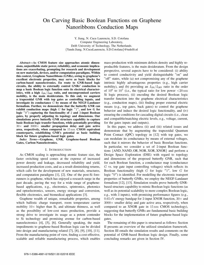
Fig. 1: Butterfly GNR dimensions.
II. SIMULATION FRAMEWORK
In this paper, we investigate the potential of using GNRs asbasic building blocks for future graphene-based logic gates,and deal with the following problem statement: Given a GNRwith a specified initial shape and a desired Boolean logictransfer function, carve the GNR geometry and modulate itsconductance (via external electric means, e.g., gate voltages),such that it reflects the desired logic functionality with goodconduction properties. To this end, we present subsequentlythe underlying GNR-based structure, the simulation modelof its electronic transport properties, followed by the designspace exploration methodology that we employ for mirroringBoolean functions onto graphene conductance.
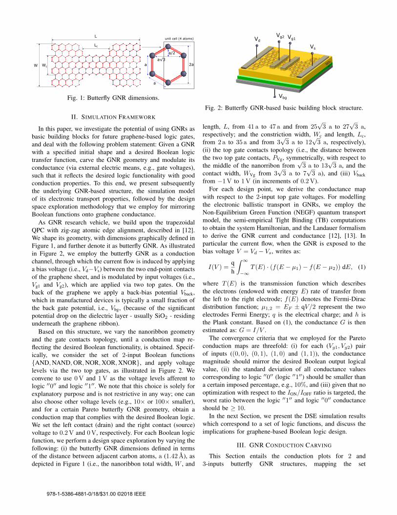
As GNR research vehicle, we build upon the trapezoidalQPC with zig-zag atomic edge alignment, described in [12].We shape its geometry, with dimensions graphically defined inFigure 1, and further denote it as butterfly GNR. As illustratedin Figure 2, we employ the butterfly GNR as a conductionchannel, through which the current flow is induced by applyinga bias voltage (i.e., Vd−Vs) between the two end-point contactsof the graphene sheet, and is modulated by input voltages (i.e.,Vg1 and Vg2), which are applied via two top gates. On theback of the graphene we apply a back-bias potential Vback,which in manufactured devices is typically a small fraction ofthe back gate potential, i.e., Vbg, (because of the significantpotential drop on the dielectric layer - usually SiO2 - residingunderneath the graphene ribbon).
Based on this structure, we vary the nanoribbon geometryand the gate contacts topology, until a conduction map re-flecting the desired Boolean functionality, is obtained. Specif-ically, we consider the set of 2-input Boolean functions{AND,NAND,OR,NOR,XOR,XNOR}, and apply voltagelevels via the two top gates, as illustrated in Figure 2. Weconvene to use 0V and 1V as the voltage levels afferent tologic ′′0′′ and logic ′′1′′. We note that this choice is solely forexplanatory purpose and is not restrictive in any way; one canalso choose other voltage levels (e.g., 10× or 100× smaller),and for a certain Pareto butterfly GNR geometry, obtain aconduction map that complies with the desired Boolean logic.We set the left contact (drain) and the right contact (source)voltage to 0.2V and 0V, respectively. For each Boolean logicfunction, we perform a design space exploration by varying thefollowing: (i) the butterfly GNR dimensions defined in termsof the distance between adjacent carbon atoms, a (1.42 A), asdepicted in Figure 1 (i.e., the nanoribbon total width, W , and
VdVg2 Vg1
Vs
SiO2
n++
Vbg
Fig. 2: Butterfly GNR-based basic building block structure.
length, L, from 41 a to 47 a and from 25√3 a to 27
√3 a,
respectively; and the constriction width, Wc and length, Lc,from 2 a to 35 a and from 3
√3 a to 12
√3 a, respectively),
(ii) the top gate contacts topology (i.e., the distance betweenthe two top gate contacts, PVg, symmetrically, with respect tothe middle of the nanorribon from
√3 a to 13
√3 a, and the
contact width, WVg from 3√3 a to 7
√3 a), and (iii) Vback
from −1V to 1V (in increments of 0.2V).For each design point, we derive the conductance map
with respect to the 2-input top gate voltages. For modellingthe electronic ballistic transport in GNRs, we employ theNon-Equilibrium Green Function (NEGF) quantum transportmodel, the semi-empirical Tight Binding (TB) computationsto obtain the system Hamiltonian, and the Landauer formalismto derive the GNR current and conductance [12], [13]. Inparticular the current flow, when the GNR is exposed to thebias voltage V = Vd − Vs, writes as:
I(V ) =qh
∫ ∞−∞
T (E) · (f(E − µ1)− f(E − µ2)) dE, (1)
where T (E) is the transmission function which describesthe electrons (endowed with energy E) rate of transfer fromthe left to the right electrode; f(E) denotes the Fermi-Diracdistribution function; µ1,2 = EF ± qV/2 represent the twoelectrodes Fermi Energy; q is the electrical charge; and h isthe Plank constant. Based on (1), the conductance G is thenestimated as: G = I/V .
The convergence criteria that we employed for the Paretoconduction maps are threefold: (i) for each (Vg1, Vg2) pairof inputs ((0, 0), (0, 1), (1, 0) and (1, 1)), the conductancemagnitude should mirror the desired Boolean output logicalvalue, (ii) the standard deviation of all conductance valuescorresponding to logic ′′0′′ (logic ′′1′′) should be smaller thana certain imposed percentage, e.g., 10%, and (iii) given that nooptimization with respect to the ION/IOFF ratio is targeted, theworst ratio between the logic ′′1′′ and logic ′′0′′ conductanceshould be ≥ 10.
In the next Section, we present the DSE simulation resultswhich correspond to a set of logic functions, and discuss theimplications for graphene-based Boolean logic design.
III. GNR CONDUCTION CARVING
This Section entails the conduction plots for 2 and3-inputs butterfly GNR structures, mapping the set
978-1-5386-4881-0/18/$31.00 ©2018 IEEE
AND OR XOR
NAND NOR XNOR
Vg10 1
1
0
Vg2
0
0 0
1
Vg10 1
1
0
Vg2
0
1
1
1
Vg10 1
1
0
Vg2
0 1
1 0
Vg10 1
1
0
Vg2
01
1 1
Vg10 1
1
0
Vg2
0
1 0
0
Vg10 1
1
0
Vg2
01
10
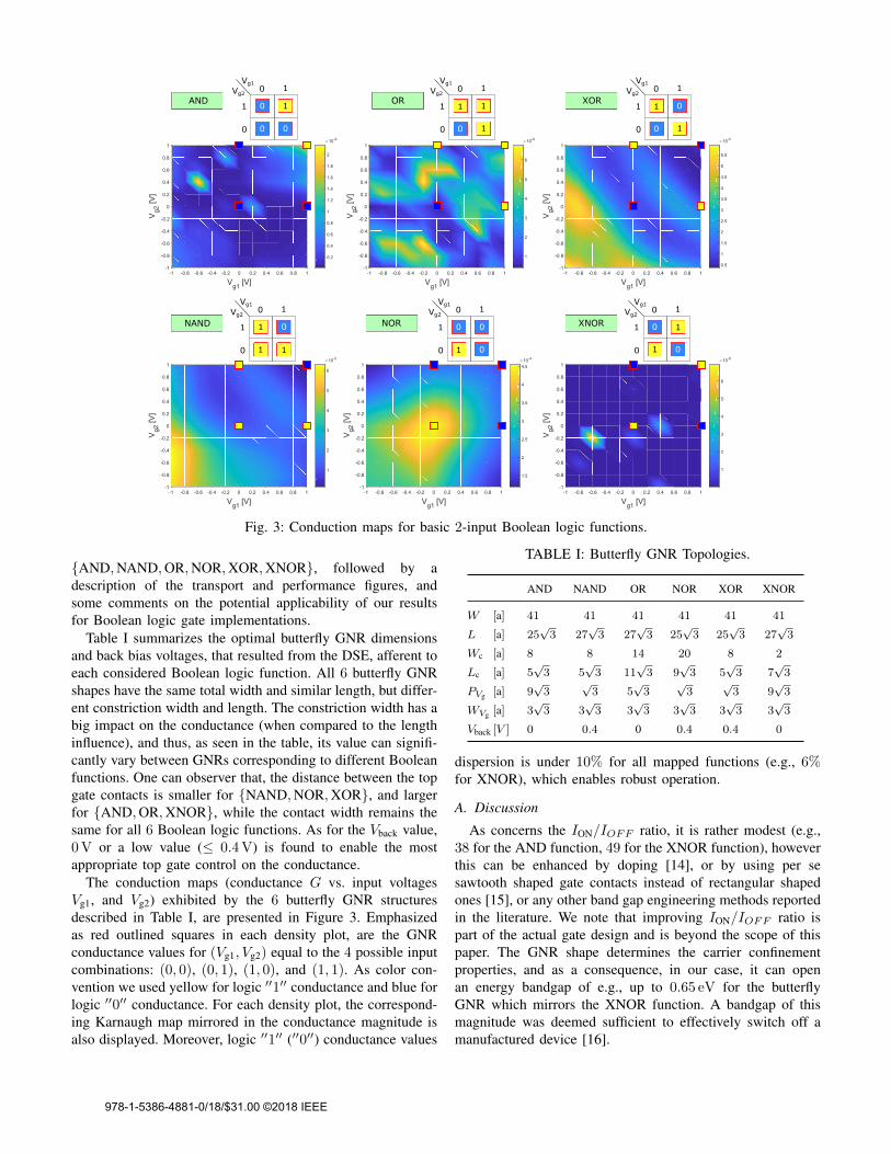
Fig. 3: Conduction maps for basic 2-input Boolean logic functions.
{AND,NAND,OR,NOR,XOR,XNOR}, followed by adescription of the transport and performance figures, andsome comments on the potential applicability of our resultsfor Boolean logic gate implementations.
Table I summarizes the optimal butterfly GNR dimensionsand back bias voltages, that resulted from the DSE, afferent toeach considered Boolean logic function. All 6 butterfly GNRshapes have the same total width and similar length, but differ-ent constriction width and length. The constriction width has abig impact on the conductance (when compared to the lengthinfluence), and thus, as seen in the table, its value can signifi-cantly vary between GNRs corresponding to different Booleanfunctions. One can observer that, the distance between the topgate contacts is smaller for {NAND,NOR,XOR}, and largerfor {AND,OR,XNOR}, while the contact width remains thesame for all 6 Boolean logic functions. As for the Vback value,0V or a low value (≤ 0.4V) is found to enable the mostappropriate top gate control on the conductance.
The conduction maps (conductance G vs. input voltagesVg1, and Vg2) exhibited by the 6 butterfly GNR structuresdescribed in Table I, are presented in Figure 3. Emphasizedas red outlined squares in each density plot, are the GNRconductance values for (Vg1, Vg2) equal to the 4 possible inputcombinations: (0, 0), (0, 1), (1, 0), and (1, 1). As color con-vention we used yellow for logic ′′1′′ conductance and blue forlogic ′′0′′ conductance. For each density plot, the correspond-ing Karnaugh map mirrored in the conductance magnitude isalso displayed. Moreover, logic ′′1′′ (′′0′′) conductance values
TABLE I: Butterfly GNR Topologies.
AND NAND OR NOR XOR XNOR
W [a] 41 41 41 41 41 41
L [a] 25√3 27
√3 27
√3 25
√3 25
√3 27
√3
Wc [a] 8 8 14 20 8 2
Lc [a] 5√3 5
√3 11
√3 9
√3 5
√3 7
√3
PVg [a] 9√3
√3 5
√3
√3
√3 9
√3
WVg [a] 3√3 3
√3 3
√3 3
√3 3
√3 3
√3
Vback [V ] 0 0.4 0 0.4 0.4 0
dispersion is under 10% for all mapped functions (e.g., 6%for XNOR), which enables robust operation.
A. Discussion
As concerns the ION/IOFF ratio, it is rather modest (e.g.,38 for the AND function, 49 for the XNOR function), howeverthis can be enhanced by doping [14], or by using per sesawtooth shaped gate contacts instead of rectangular shapedones [15], or any other band gap engineering methods reportedin the literature. We note that improving ION/IOFF ratio ispart of the actual gate design and is beyond the scope of thispaper. The GNR shape determines the carrier confinementproperties, and as a consequence, in our case, it can openan energy bandgap of e.g., up to 0.65 eV for the butterflyGNR which mirrors the XNOR function. A bandgap of thismagnitude was deemed sufficient to effectively switch off amanufactured device [16].
978-1-5386-4881-0/18/$31.00 ©2018 IEEE
Vg1
Vg1
Cox
Cq
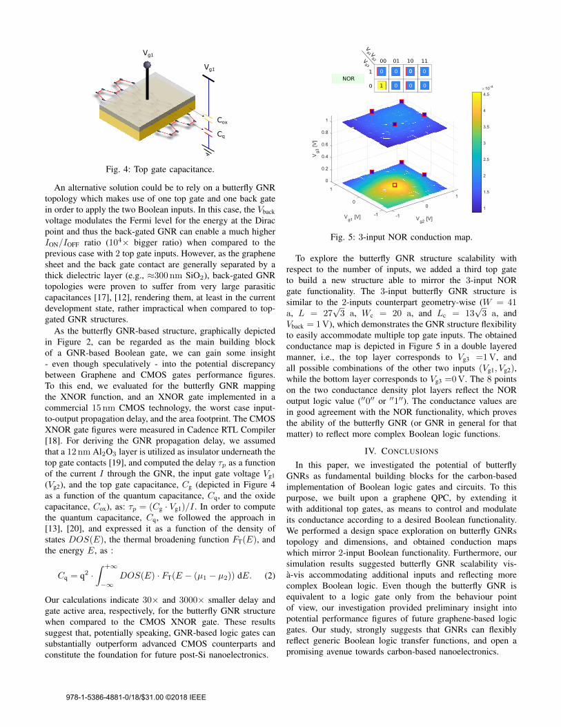
Fig. 4: Top gate capacitance.
An alternative solution could be to rely on a butterfly GNRtopology which makes use of one top gate and one back gatein order to apply the two Boolean inputs. In this case, the Vbackvoltage modulates the Fermi level for the energy at the Diracpoint and thus the back-gated GNR can enable a much higherION/IOFF ratio (104× bigger ratio) when compared to theprevious case with 2 top gate inputs. However, as the graphenesheet and the back gate contact are generally separated by athick dielectric layer (e.g., ≈300 nm SiO2), back-gated GNRtopologies were proven to suffer from very large parasiticcapacitances [17], [12], rendering them, at least in the currentdevelopment state, rather impractical when compared to top-gated GNR structures.
As the butterfly GNR-based structure, graphically depictedin Figure 2, can be regarded as the main building blockof a GNR-based Boolean gate, we can gain some insight- even though speculatively - into the potential discrepancybetween Graphene and CMOS gates performance figures.To this end, we evaluated for the butterfly GNR mappingthe XNOR function, and an XNOR gate implemented in acommercial 15 nm CMOS technology, the worst case input-to-output propagation delay, and the area footprint. The CMOSXNOR gate figures were measured in Cadence RTL Compiler[18]. For deriving the GNR propagation delay, we assumedthat a 12 nm Al2O3 layer is utilized as insulator underneath thetop gate contacts [19], and computed the delay τp as a functionof the current I through the GNR, the input gate voltage Vg1(Vg2), and the top gate capacitance, Cg (depicted in Figure 4as a function of the quantum capacitance, Cq, and the oxidecapacitance, Cox), as: τp = (Cg · Vg1)/I . In order to computethe quantum capacitance, Cq, we followed the approach in[13], [20], and expressed it as a function of the density ofstates DOS(E), the thermal broadening function FT(E), andthe energy E, as :
Cq = q2 ·∫ +∞
−∞DOS(E) · FT(E − (µ1 − µ2)) dE. (2)
Our calculations indicate 30× and 3000× smaller delay andgate active area, respectively, for the butterfly GNR structurewhen compared to the CMOS XNOR gate. These resultssuggest that, potentially speaking, GNR-based logic gates cansubstantially outperform advanced CMOS counterparts andconstitute the foundation for future post-Si nanoelectronics.
NOR
Vg1 V
g2 00
1
0
Vg3
00
01
01 10
0 0
00 0
11
Fig. 5: 3-input NOR conduction map.
To explore the butterfly GNR structure scalability withrespect to the number of inputs, we added a third top gateto build a new structure able to mirror the 3-input NORgate functionality. The 3-input butterfly GNR structure issimilar to the 2-inputs counterpart geometry-wise (W = 41a, L = 27
√3 a, Wc = 20 a, and Lc = 13
√3 a, and
Vback = 1V), which demonstrates the GNR structure flexibilityto easily accommodate multiple top gate inputs. The obtainedconductance map is depicted in Figure 5 in a double layeredmanner, i.e., the top layer corresponds to Vg3 =1V, andall possible combinations of the other two inputs (Vg1, Vg2),while the bottom layer corresponds to Vg3 =0V. The 8 pointson the two conductance density plot layers reflect the NORoutput logic value (′′0′′ or ′′1′′). The conductance values arein good agreement with the NOR functionality, which provesthe ability of the butterfly GNR (or GNR in general for thatmatter) to reflect more complex Boolean logic functions.
IV. CONCLUSIONS
In this paper, we investigated the potential of butterflyGNRs as fundamental building blocks for the carbon-basedimplementation of Boolean logic gates and circuits. To thispurpose, we built upon a graphene QPC, by extending itwith additional top gates, as means to control and modulateits conductance according to a desired Boolean functionality.We performed a design space exploration on butterfly GNRstopology and dimensions, and obtained conduction mapswhich mirror 2-input Boolean functionality. Furthermore, oursimulation results suggested butterfly GNR scalability vis-a-vis accommodating additional inputs and reflecting morecomplex Boolean logic. Even though the butterfly GNR isequivalent to a logic gate only from the behaviour pointof view, our investigation provided preliminary insight intopotential performance figures of future graphene-based logicgates. Our study, strongly suggests that GNRs can flexiblyreflect generic Boolean logic transfer functions, and open apromising avenue towards carbon-based nanoelectronics.
978-1-5386-4881-0/18/$31.00 ©2018 IEEE
REFERENCES
[1] Liou, J. J. and Schwierz, F. and Wong, H., Nanometer CMOS. PanStandford Publishing, 2010.
[2] Rupp, K. and Siegfried, S., “The economic limit to Moore’s law.” inIEEE Transactions on Semiconductor Manufacturing, vol. 24, no. 1,2011, pp. 1–4.
[3] Ferrari, A.C. and et al., “Science and technology roadmap for graphenerelated 2D crystals, and hybrid systems.” in Nanoscale, vol. 7, no. 11,2015, pp. 4587–5062.
[4] Choi, W. and Lee, J. W., Graphene Syntehsis and Applications. CRCPress, 2012.
[5] J. M. Allen, V. C. Tung, and R. B. Kaner, “Honeycomb carbon: a reviewof graphene.” in Chemical Reviews, vol. 110, no. 1, 2010, pp. 132–145.
[6] Matsumoto, K., Frontiers of graphene and carbon nanotubes - devicesand applications. Springer Japan, 2015.
[7] A. H. Castro Neto and et al., “The electronic properties of graphene.”in Reviews of Modern Physics, vol. 81, no. 1, 2009, pp. 109–162.
[8] W. Ren and H. M. Cheng, “The global growth of graphene.” in NatureNanotechnology, vol. 9, 2014, pp. 726–730.
[9] Z. F. Wang and et al., “Emerging nanodevice paradigm: Graphene-basedelectronics for nanoscale computing.” in ACM Journal on EmergingTechnologies in Computing Systems (JETC), vol. 5, no. 1, 2009, pp.1–19.
[10] M. R. Stan and et al., “Graphene devices, interconnect and circuits
- challenges and opportunities.” in IEEE International Symposium onCircuits and Systems (ISCAS), 2009, pp. 69–72.
[11] M. J. Marmolejo and J. Velasco-Medina, “Review on graphene nanorib-bon devices for logic applications.” in Microelectronics Journal, vol. 48,2016, pp. 18–38.
[12] Karafyllidis, I., “Current switching in graphene quantum point contacts.”in IEEE Transactions on Nanotechnology, vol. 13, no. 4, 2014, pp. 820–824.
[13] Datta, S., Quantum transport: Atom to transistor. Cambridge UniversityPress, 2005.
[14] T. Ohta, A. Bostwick, T. Seyller, and et al., “Controlling the ElectronicStructure of Bilayer Graphene.” in Science, vol. 313, no. 5789, 2006,pp. 951–954.
[15] M. S. Jang and et al., “Graphene field effect transistor without an energygap.” in Proceedings of the National Academy of Sciences of the UnitedStates of America, vol. 110, no. 22, 2013, pp. 8786–8789.
[16] L. Xi and et al., “Chemically derived, ultrasmooth graphene nanoribbonsemiconductors.” in Science, vol. 319, no. 5867, 2008, pp. 1229–1232.
[17] Novoselov, K. S. and et al., “Electric field effect in atomically thincarbon films.” in Science, vol. 306, 2004, pp. 666–669.
[18] Cadence. [Online]. Available: https://www.cadence.com/.[19] S. Drscher and et al., “Quantum capacitance and density of states of
graphene.” in Physica Scripta, vol. T146, 2012, pp. 1–5.[20] M. Mousavi-Khoshdel, E. Targholi, and M. J. M., “First-principles cal-
culation of quantum capacitance of codoped graphenes as supercapacitorelectrodes.” in Physica Scripta, vol. T146, 2012, pp. 26 290–26 295.
978-1-5386-4881-0/18/$31.00 ©2018 IEEE