on ed-32, high-speed modulation of semiconductor...
TRANSCRIPT

2512 IEEI', TRANSACTIONS ON ELECTRON DEVICES, VOL. ED-32, NO, 12, DECEMBER 1985
High-speed Modulation of Semiconductor Lasers
(hvited Paper)
Abstract-An overview is given of the direct modulation performance of high-speed semiconductor lasers. The high-speed response charac- teristics are described using a cascaded two-port model of the laser. This model separates the electrical parasitics from the intrinsic laser and enables these subsections to be considered separately. The presen- tation concentrates on the small-signal intensity modulation and fre- quency modulation responses, and the large-signal switching tra~nsients and chirping. Device-dependent limitations on high-speed Performance are explored and circuit modeling techniques are briefly reviewc'd.
R I. INTRODUCTION
ECENT DEVELOPMENTS in semiconductor laser fabrication have led to dramatic improvements in
high-speed direct modulation performance. Bandwidths of 15-16 GHz have been achieved at room temperature: [ l] , [2], while figures as high as 22 GHz have been obtained with cooled lasers [3]. Non-return-to-zero (NRZ) pulse code modulation has been reported at bit rates up to 8 Gbit/s [2]-[4].
The availability of high-speed lasers has stimulafed a variety of new applications in communications and si.gnal processing. Very high bit-rate data transmission over long lengths of optical fiber has been demonstrated in a number of laboratories [5]-[7], while analog transmission of mi- crowave signals provides an alternative to digital methods in some circumstances [8]. Other applications of high- speed lasers include optically controlled microwave switches [9], optical injection-locking of electronic cwil- lators [lo], and optical fiber delay-line filter networks [I l l .
The principal attraction of the direct modulation tech- nique is its simplicity. With the laser biased above thres- hold and a modulation signal superimposed on the drive current, the output optical power of the laser is an analog of the modulation waveform. In most applications the modulated envelope of the output power is of prime i:?ter- est, but it is important to recognize that the output oFtical frequency also varies in response to the signal compcnent of the drive current [12]. This frequency deviation i.s of potential use as a modulation format in coherent conmu- nication systems [ 131 but manifests itself as an undesirable frequency chirp which causes a dispersion penalty in high bit-rate long-haul direct detection systems [14], [ 151.
This paper gives an overview of the direct modulation performance of high-speed semiconductor lasers. The general form of the response characteristics is described, and the main factors limiting the high-speed performance are identified. The presentation focuses on the small-sig- nal intensity modulation (IM) and frequency modulation (FM) behavior, and the large-signal switching transients and chirping. The paper is organized as follows: Section I1 introduces the concept of a cascaded two-port model of the laser with electrical parasitics separating the external contacts from the intrinsic laser. The parasitics are con- sidered in detail in Section 111, and methods for minimiz- ing stray resistance and capacitance are described. Sec- tions IV-VI cover the small-signal and large-signal modulation characteristics of the intrinsic laser diode, with emphasis on device-dependent limitations on high-speed performance. Circuit modeling of semiconductor lasers is briefly reviewed in Section VII.
11. TWO-PORT MODEL A two-port black-box model of the semiconductor laser
is shown in Fig. 1. This model identifies the input-output variables of interest and summarizes the main effects of the parasitics on the overall response of the laser. The in- put variables' are the drive current Z and the drive voltage V. The drive current and voltage seen by the intrinsic laser are Z i and V, respectively, while the output variables are the optical power P and the optical frequency shift Av. This description of the output signal using two variables is strictly valid only in single-frequency devices such as distributed feedback (DFB) lasers [ 161, where the output power is contained almost entirely in single longitudinal mode. In a conventional single-cavity Fabry-Perot reso- nator laser the picture is more complicated because the output power can be distributed over a number of longi- tudinal modes. Furthermore, this distribution may vary with time, particularly if the laser is modulated [ 171. In the present paper, Av represents the frequency shift of the central longitudinal mode.
The laser in Fig. 1 is divided into three main cascaded subsections: the package or mount parasitics, the para- sitics associated with the semiconductor chip, and the in- trinsic laser (active layer and cavity). Parasitics associated
Manuscript received June 7, 1985; revised July 24, 1985. The author is with AT&T Bell Laboratories, Crawford Hill Laboratory, ' Upper case symbols are used for instantaneous and steady-state values,
Holmdel, NJ 07733. while small-signal quantities are indicated by lower case symbols.
0018-9383/85/1200-2572$01.00 @ 1985 IEEE
TUCKER: HIGH-SPEED MODULATION OF SEMICONDUCTOR LASERS 2513
INF'UT OUTPUT 2 p m ~ - 2 5 0 p n - - - I. PARASlTlCS I A INTRINSIC
-+ LASER
t V OR MOUNT; I VA
,p A u I
1 1 OVERALL RESPONSES
SMALL-SIGNAL * b\. => h, RESPCINSES
I W
SMALL-SIGNAL RESPCINSES
W W -'FM
v t r t r t
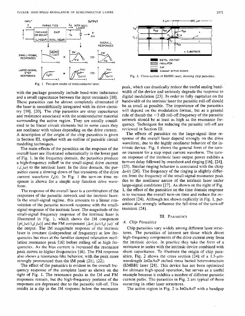
Fig. 1. Two-port model of semiconductor laser.
with thle package generally include bond-wire inductance and a small capacitance between the input terminals [HI. These parasitics can be almost completely eliminated if the laser is monolithically integrated with its drive circui- try [19], [20]. The chip parasitics are stray capacitance and resistance associated with the semiconductor material surroulnding the active region. They are usually consid- ered to be linear circuit elements but in some cases they are nonlinear with values depending on the drive current. A description of the origin of the chip parasitics is given in Section 111, together with an outline of parasitic circuit modeling techniques.
The main effects of the parasitics on the response of the overall laser are illustrated schematically in the lower part of Fig. 1. In the frequency domain, the parasitics produce a high-frequency rolloff in the small-signal drive current iA(jw) to the intrinsic laser. In the time domain, the par- asitics cause a slowing-down of fast transients of the drive current waveform IA(t). In Fig. 1 the turn-on time re- sponse: is shown for a simple step function drive wave- form.
The response of the overall laser is a combination of the responses of the parasitic network and the intrinsic laser. In the small-signal regime, this amounts to a linear con- volution of the parasitic network response with the small- signal response of the intrinsic laser. The magnitude of the small-,signal frequency response of the intrinsic laser is illustrated in Fig. 1, which shows the IM component 1 p( jw)/iA( jw) I and the FM component 1 Av( jw)/iA( jw) I of the output. The IM magnitude response of the intrinsic laser is constant (independent of frequency) at low fre- quencies but rises at the familiar damped relaxation oscil- lation resonance peak [16] before rolling off at high fre- quencies. As the bias current is increased the resonance peak moves to higher frequencies [ 161. The FM response also shows a resonance-like behavior, with the peak more strongly pronounced than the IM peak [21], [22],
The effect of the parasitics is evident in the overall fre- quency response of the complete laser as shown on the right oif Fig. 1. The resonance peaks in the IM and FM responses remain, but the high-frequency portions of the responses are depressed due to the parasitic roll-off. This results in a dip in the IM response below the resonance
m--\ n SUBSTRATE
= METAL CONTACT INSULATOR 0 I n P
InGaAsP ACTIVE REGION
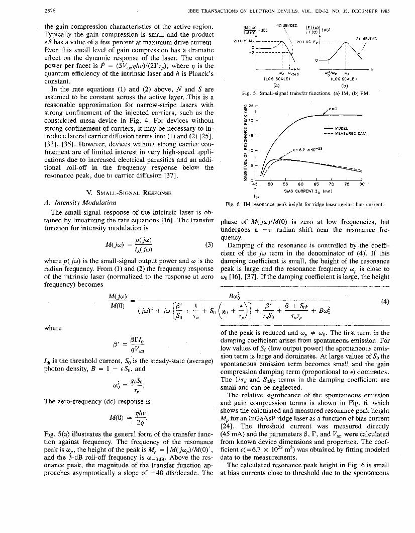
Fig. 2. Cross-section of EMBH laser, showing chip parasitics.
peak, which can drastically reduce the useful analog band- width of the device and seriously degrade the response to digital modulation [23]. In order to fully capitalize on the bandwidth of the intrinsic laser the parasitic roll-off should be as small as possible. The importance of the parasitics will depend on the modulation format, but as a general rule of thumb the - 3 dB roll-off frequency of the parasitic network should be at least as high as the resonance fre- quency. Techniques for reducing the parasitic roll-off are reviewed in Section 111.
The effects of parasitics on the large:-signal time re- sponse of the overall laser depend strongly on the drive waveform, due to the highly nonlinear behavior of the in- trinsic device. Fig. 1 shows the general form of the turn- on transient for a step input current waveform. The turn- on response of the intrinsic laser output power exhibits a turn-on delay followed by overshoot and ringing [ 161, [24], [25]. Similar ringing behavior is associatied with the chirp Av( t ) [26]. The frequency of the ringing is slightly differ- ent from the frequency of the small-signal resonance peak due to the nonlinear nature of the intrinsic laser under large-signal conditions [27]. As shown on the right of Fig. 1, the effect of the parasitics on the time {domain response is to increase the overall turn-on time and reduce the ov- ershoot [24]. Although not shown explicitly in Fig. 1, par- asitics also strongly influence the fall-time of the turn-off transient [24].
111. PARASITES A . Chip Parasitics
Chip parasitics vary widely among different laser struc- tures. The parasitics of interest are those which divert high-frequency components of the drive current away from the intrinsic device. In practice they talke the form of a resistance in series with the intrinsic device combined with shunt capacitance. To illustrate the origin of chip para- sitics, Fig. 2 shows the cross section [24] of a 1.3-pm- wavelength InGaAsP etched mesa buried heterostructure (EMBH) laser [28]. This device has not been optimized for ultimate high-speed operation, but serves as a useful example because it exhibits a number of different parasitic current paths. The parasitics in Fig. 2 ar'e typical of those occurring in other laser structures.
The active region in Fig. 2 is InGaAsP with a bandgap

2574 IEEE TRANSACTIONS ON ELECTRON DEVICES, VOL. ED-32, NO. 12, DECEMBER 1985
corresponding to a wavelength of 1.3 pm. It is surrounded on all four sides by InP. The resistance R, of the contact and the p-region above the active region combined with resistance R,, of the substrate below the active region gives a total resistance of R, = R, + R,, in series with the intrinsic device. The small-signal input resistance of the intrinsic laser is typically less than 1 C! at currents above threshold [ 181 due to clamping of the Fermi levels. On the other hand R, can take values in the range 3-10 and dominates the total input resistance. The time constant characterizing the parasitic roll-off is the product of R, and the effective shunt capacitance. The main sources of $,hunt capacitance are as follows [24].
I ) Reverse-Biased Blocking Junction: Under normal operating conditions, with the intrinsic device forward- biased, the p-n junction between the upper n-layer and the p isolation layer is weakly reverse-biased. This rev8:rse- biased junction serves as a block to dc current, thereby reducing dc leakage. The space-charge capacitance C L of this junction can be quite large as it usually extends across the entire area of the chip. Typically, C, is of the order of 100 pF. One parasitic high-frequency'current path follows the upper n-layer from the top contact and passes thr'mgh the blocking junction capacitance to ground. Since the up- per n-layer has a nonzero resistance, this current path can be modeled as a distributed RC network. It is represented in Fig. 2 as a lumped approximation with coupling resis- tances RNi. Depending on the thickness and resistivity of the n-layer, the effective capacitance of the blocking junc- tion, as seen from the top contact, will decrease at high frequencies. The larger the value of the resistances K,, the less efficient this current path is at bypassing high- frequency components of drive current away from thc in- trinsic laser.
2) MIS Isolation Layer: The insulator layer under the top metal contact in Fig. 2 acts as a metal-insulator-scmi- conductor (MIS) capacitance C, distributed across the chip surface. A typical value for this capacitance is approxi- mately 10 pF for a 500 X 250 pm chip area and a 0.2-pm- thick silicon nitride insulator layer. The MIS capacitimce CN appears in series with the blocking junction capaci- tance C,, which is usually much larger than CN. The 'Lata1 capacitance from the top contact through CN to ground is therefore approximately equal to CN. Since CN extmds across the entire area of the top contact, the total rosis- tance in series with CN is low ( - 0.5 a). Consequently, CN serves as a very efficient bypass for high-frequency cur- rent away from the active region [24].
3) Forward-Biased Junction Adjacent to Active Re- gion: The third high-frequency parasitic current path fol- lows the thin resistive p-layer and the capacitance Cdr as- sociated with the forward-biased region of the p-n junction adjacent to the active layer. There is also a dc leakage :path in shunt with CJ, but this is omitted in Fig. 2 for simplic- ity. Since CJ,is the capacitance of a forward-biased junc- tion, it can take on large values ( - 1000 pF), depending on details of the device geometry and the magnitude of the dc leakage current. It is likely that CJ is important in
INTRINSIC LASER
Fig. 3. Circuit model of package and chip parasitics.
devices with weak lateral current confinement, such as channeled substrate planar (CSP) lasers. Unlike the par- asitic capacitances in 1) and 2) above, CJ depends strongly on the dc current through the forward-biased junction. This results in a bias-dependent parasitic roll-off. The im- portance of CJ in determining the parsitic roll-off depends on the value of the series resistance RJ of the thin p-layer. If RJ is more than about 1 Q, the effect of CJ will be small.
B. Evaluation of Parasitics The parasitic paths described in 1)-3) above are reason-
ably complex, and may be difficult to characterize pre- cisely. A simplified circuit model of the chip parasitics is given in Fig. 3, combined with the package parasitics (bondwire inductance Lp, small loss resistance Rp, and standoff capacitance C, associated with the ceramic con- tact pad [ 181). In a given laser, one of the parasitic paths 1)-3) above will usually dominate. Therefore Fig. 3 shows just one chip parasitic capacitance. Where necessary, the model can be generalized to include additional shunt paths. The capacitance C, is the effective shunt parasitic capacitance and R, is the resistance in series with the in- trinsic laser. If the dominant parasitic capacitance is CJ in 3) above, then the effective value of R, is reduced because RJ connects to the p-region above the active layer at a point in close proximity to the active region. The current gen- erator ZL models dc leakage around the active region [29].
The signal generator in Fig. 3 has a source resistance R I N which is typically 50 or 100 in systems using con- ventional microwave test instrumentation. If the laser is driven directly from an active device such as a transistor, RIN is larger. The parasitic circuit is terminated with the intrinsic laser. Since the small-signal input resistance of the intrinsic laser is small it can be replaced by a short circuit with negligible loss of accuracy in calculations of the high-frequency parasitic roll-off.
A convenient method for determining values of the par- asitics in Fig. 3 is to fit the model to measured electrical scattering parameters over a range of frequencies. The transfer function of the model in Fig. 3 can then be cal- culated and the influence of the parasitics thereby evalu- ated. Measurements of the parasitics by scattering param- eter techniques have been described elsewhere [ 181, [24], [30], [31]. Similarly, calculations of the parasitic roll-off have been described in [18], [24], and [30]. The main findings of these studies are summarized below.
i) The stand-off capacitance Cp has little effect on the response for low K I N (I 50 Q) but can resonate with Lp to give a weakly enhanced response for large RIN ( > 100 Q ) .

TUCKER: HIGH-SPEED MODULATION OF SEMICONDUCTOR LASERS 2575
helps to minimize parasitic contact resistance. The para-
corresponds to a -3 dB roll-off frequency of more than 24 GHz.
p / L m sitic R,C, product for the constricted mesa device in [3]
Iv. RATE EQUATIONS AND DAhlPING
n + I n P SUBSTRATE The dynamics of the intrinsic device are central to the modulation response of the overall laser. In the following sections the high-speed modulation properties of the in-
= METAL CONTACT trinsic laser are explored using the well-known rate equa- 0 s i 02 tions [16], [33]. The objective here is to provide an un-
InGaAsP ACTIVE REGION derstanding of the modulation response amd to obtain an Fig. 4. Cross section of constricted mesa laser. estimate of limitations on bandwidth and switching speed. I
ii) If the bond wire inductance Lp is small ( I 0.2 nH), it has little effect on the response up to 20 GHz. Low in- ductances of this order can be achieved using short ( c 0.5 mm) wire and/or with tape or mesh replacing the usual thin wilre. If Lp 1 1 nH, then Lp can cause significant roll- off in the response above about 6 GHz with RIN = 50 Q. If RIN <: 50 Q, this inductive roll-off occurs at lower fre- quencies.
iii) For small Lp, the dominant elements affecting the high-frequency parasitic roll-off are the R,C, parasitics in the chip. It is essential that these parasitics be minimized if high-speed operation is to be achieved. C: Low-Parasitic Devices
A number of new low-parasitic device structures have been reported [ 11-[4]. One class of such structures uses a semi-insulating substrate in place of the conducting sub- strate in Fig. 2. The semi-insulating substrate leads to a resistance in series with CN and C,. These capacitances become part of a distributed RC network, and the effective capacitance is reduced at high frequencies. Lau and Yariv [30] have reported values of C, and R, as low as 3 pF and 2.5 Q, :respectively, in an AlGaAs laser on a semi-insulat- ing substrate. The corresponding -3 dB roll-off fre- quency, due to the parasitics, is approximately 20 GHz. Koren [4] has reported a similar device in InGaAsP.
Low parasitics can also be achieved on conducting sub- strates. Two examples are the vapor phase regrown laser of Su et al. [ l ] and the constricted mesa or mushroom stripe laser used by Bowers et al. [2], [3]. Fig. 4 shows the cross section of the constricted mesa laser. There are a number of special features in this structure which help to minlmize parasitics. First, the quaternary material on each side of the active region is removed by etching. The gap under the resulting “mushroom stripe” is filled with S i 0 2 in order to block leakage current. Since there is no reverse:-biased blocking junction, the capacitance between the mushroom stripe and the nf InP substrate is small ( - 0.2 pF). Second, removal of the quaternary material beside the active layer eliminates any forward-biased junc- tion adjacent to the active layer. Consequently the capac- itance C, in Fig. 2 is zero for this laser. Third, the bond- ing-pad capacitance is made small by minimizing the pad area, a.nd using a relatively thick ( - 1.5 pm) polyimide layer under the contact. Finally, the pf InGaAsP cap layer
A number of mechanisms can cause damping ofthe res- onance in the modulation response. These include spon- taneous emission coupled into the lasing mode [34], spa- tial hole burning combined with carrier diffusion [35]- [37], and nonlinearities due to spectral hole burning [38]- [41] and nonlinear (two-photon) absorption [42]. In prac- tical lasers the resonance is strongly damped and sponta- neous coupling alone cannot account for the observed damping behavior [43]. Measurements of FM (see later) and other studies of damping behavior [41] suggest that spectral hole burning is the dominant dam:ping mechanism in narrow-stripe InGaAsP devices. In general, however, diffusion, spectral hole burning, and nonlinear absorption all contribute to damping. In the rate equa.tions used here, the diffusion [43] and nonlinear effects I1241 are lumped together as an effective field-dependent optical gain compression. This is a phenomenological approach which enables numerical values for the damping factors to be de- termined by fitting the rate equations to measured data [24]. Strictly speaking, carrier diffusion, two-photon ab- sorption, and gain compression due to spectral hole burn- ing should enter the rate equations as separate terms, but the approximate approach is used here because it leads to simple analytical expressions for bandwidth. The analysis is restricted to single-frequency and nearly single-fre- quency lasers, which can be described by single-mode rate equations. However, the results also serve ,as a useful guide to the modulation behavior of multimode devices.
The single-mode rate equations are written as follows:
where N is the electron density, S is the photon density, I’ is the optical confinement factor given by the ratio of the active region volume to the modal vo1urn.e [16], go is the gain slope constant, Nog is the electron density at which the net gain is zero, rp is the photon lifetime, r, is the electron lifetime, p is the fraction of spontaneous emis- sion coupled into the laser mode, V,,, is the volume of the active layer, q is the electronic charge, and ZA is the cur- rent injected into the active layer (Fig. l). The parameter E is a small number (with units of volume:) which specifies
2576 IEEE TRANSACTIONS ON ELECTRON DEVICES, VOL. ED-32, NO. 12, DECEMBER 1985
the gain compression characteristics of the active region. Typically the gain compression is small and the pxduct E S has a value of a few percent at maximum drive current. Even this small level of gain compression has a dramatic effect on the dynamic response of the laser. The output power per facet is P = (SVa,,yhv)/(21‘rp), where r is the quantum efficiency of the intrinsic laser and h is Planck’s constant.
In the rate equations (1) and (2) above, N and S are assumed to be constant across the active layer. This is a reasonable approximation for narrow-stripe lasers with strong confinement of the injected carriers, such as the constricted mesa device in Fig. 4. For devices without strong confinement of carriers, it may be necessary to in- troduce lateral carrier diffusion terms into (1) and (2) [25], [33], [35]. However, devices without strong carriel” con- finement are of limited interest in very high-speed sppli- cations due to increased electrical parasitics and an addi- tional roll-off in the frequency response below the resonance peak, due to carrier diffusion [37].
V. SMALL-SIGNAL RESPONSE A . Intensity Modulation
The small-signal response of the intrinsic laser is ob- tained by linearizing the rate equations [16]. The transfer function for intensity modulation is
where p ( j w ) is the small-signal output power and w .is the radian frequency. From (1) and (2) the frequency response of the intrinsic laser (normalized to the response at zero frequency) becomes
- MODEL - -- MEASURED DATA
E = 6.7 X 10⁻²³
3
t BIAS CURRENT I, ( m A ) I t h
Fig. 6. IM resonance peak height for ridge laser against bias current.
phase of M( jw) /M(O) is zero at low frequencies, but undergoes a -T radian shift near the resonance fre- quency.
Damping of the resonance is controlled by the coeffi- cient of the j w term in the denominator of (4)’. If this damping coefficient is small, the height of the resonance peak is large and the resonance frequency up is close to wo [ 161, [37]. If the damping coefficient is large, the height
where
Ith is the threshold current, So is the steady-state (average) photon density, B = 1 - €SO, and
TP
The zero-frequency (dc) response is
Fig. 5(a) illustrates the general form of the transfer func- tion against frequency. The frequency of the resonance peak is up, the height of the peak is Mp = 1 M( j w J M ( 0 ) 1 , and the 3-dB roll-off frequency is W-3dB. Above the res- onance peak, the magnitude of the transfer functior: ap- proaches asymptotically a slope of -40 dB/decade. The
of the peak is reduced and up it wo. The first term in the damping coefficient arises from spontaneous emission. For low values of So (low output power) the spontaneous emis- sion term is large and dominates. At large values of So the spontaneous emission term becomes small and the gain compression damping term (proportional to E ) dominates. The l /rn and Sogo terms in the damping coefficient are small and can be neglected.
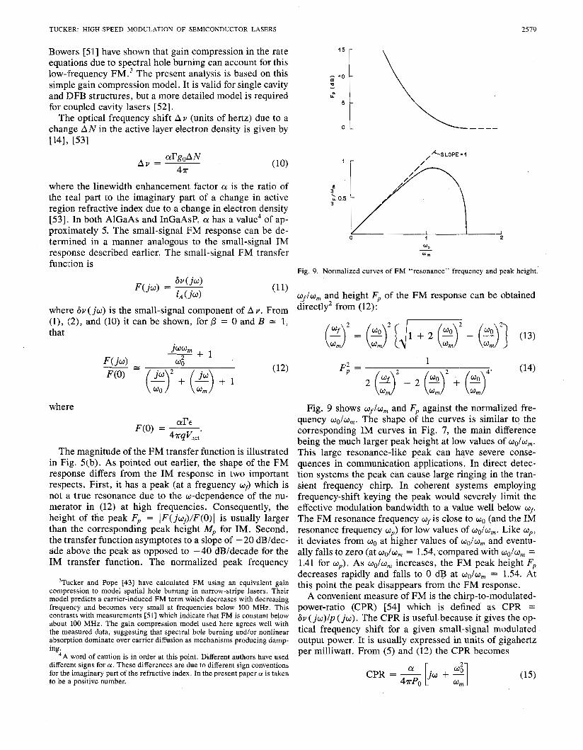
The relative significance of the spontaneous emission and gain compression terms is shown in Fig. 6, which shows the calculated and measured resonance peak height Mp for an InGaAsP ridge laser as a function of bias current [24]. The threshold current was measured directly (45 mA) and the parameters 0, r, and Vact were calculated from known device dimensions and properties. The coef- ficient E ( =6.7 X m3) was obtained by fitting modeled data to the measurements.
The calculated resonance peak height in Fig. 6 is small at bias currents close to threshold due to the spontaneous

TUCKER: HIGH-SPEED MODULATION OF SEMICONDUCTOR LASERS 2577
emission term in the damping coefficient. For bias cur- rents above 53 mA, the peak height Mp decreases due to the increasing gain compression term. Also shown in Fig. 6 is the calculated Mp for zero gain compression (e = 0). In this case the calculated Mp rises to a value of approxi- mately 22 dB at high currents. This is much larger than is observed experimentally [24], indicating that sponta- neous emission alone cannot account for the observed damping behavior.
In the analysis summarized below it is assumed that the device is operated in the regime well above threshold, where gain compression damping dominates. In addition, it is assumed that Bug = wg in (4). This simplification introduces small errors in the calculated bandwidth at large power levels, but leads to simple analytical solutions. With p’ = 0 and with other small terms neglected, (4) reduces to
where w, is a bias-independent parameter given by w, = go/€. This frequency 0, is related to the damping time constant T~ [37] as follows
Urn 71 = -
It is shown below that w, is a useful normalization param- eter and serves as a measure of the maximum achievable bandwidth.
B. High-Frequency Limitations2 In this section, limitations on the small-signal IM band-
width of the intrinsic laser are explored. The main param- eters of interest in this context are the resonance fre- quency up, the - 3-dB frequency W-3dB, and the height Mp of the resonance peak. From (5), it is a straightforward matter to show that
wg
and
Note that all frequencies here are normalized to w,. This lead,s to normalized curves of up, w - 3 dB, and Mp which are independent of laser parameters and can therefore be applied to any device.
’This work has not been previously published.
Fig. 7. Normalized curves of IM resonance frequency, -3-dB frequency, and resonance peak height.
The normalized curves are shown in Fig. 7. Since w, is independent of the bias current, and (rj0 is proportional to a, the dependent variable wo/u, on the horizontal axis of Fig. 7 scales as the square root of the steady-state op- tical output power. At low and moderate output power lev- els (wo/w, c 0.4), the normalized resonance frequency w,,/w, rises with a slope close to unity, such that up = wo [ 161, [44]. At higher power levels up becomes smaller than wo, and u p / w , reaches a maximum value of 1/& at wo/w, = 1.0. For values of wo/w, above 1.0, wp falls rapidly and reaches zero at wo/w, = h. The -3-tiB frequency u - 3 d B
is greater than wo for wo/w, up to J z . At this point, @-3dB
saturates at its maximum value ( h u m ) and then slowly decreases with increasing wo. The maximum achievable -3-dB bandwidth is therefore &wl,. The resonance height Mp is relatively large at low output power levels (recall that spontaneous emission damping is ignored here) and decreases with increasing output power. The value of Mp falls to 0 dB at wo/w, = h. At this point the reso- nance peak disappears and the response becomes maxi- mally flat (second-order Butterworth) 1[45].
In addition to the damping-induced saturation of band- width shown in Fig. 7, there are a number of other mech- ,
anisms which can increase the curvature in the w - ~ ~ ~ ver- sus a characteristic. At high power levels the temperature of the active region increases. This can lead to a reduction in the gain slope go and a corresponding reduction in wo. For devices with si,gnificant chip and package parasitics, the parasitic roll-off also accentuates the curvature of the w W 3 d B characteristic [42].
Semiconductor lasers are normally operated at power levels where wo/w, is less than 1 and the W-3dB versus Go characteristic is approximately linear. As an example,

2578 IEEE TR4WSACTIONS ON ELECTRON DEVICES, VOL. ED-32, NO. 12, DECEMBER 1985
the triangles in Fig. 7 are measured values of up, W - 3 d s s
and Mp for a 1.55-pm EMBH laser [28] at output power levels of 1, 2, 3, and 4 mW. These data were obtained as follows. The small-signal frequency response and elect1"i- cal reflection coefficient were measured using a micra- wave network analyzer and a high-speed photodiode [24] ~
The electrical parasitics were determined from the reflec- tion coefficient [24] and the roll-off due to the parasitics was extracted from the measured overall response to give the frequency response of the intrinsic laser. The fre- quency f, = w,/2n was determined from device pararn- eters obtained by matching the modeled and measured fre- quency responses [24]. The value for f, obtained in this way was 8.5 GHz. Thus the theoretical maximum achiev- able -3-dB bandwidth for the intrinsic laser is 12 GHz at an output power of approximately 12 mW. However, power levels as high as this may be difficult to achieve for reaso:w outlined below.
C. Design Considerations for Wide-Band Lasers Ideally, a wide-band laser should have a large -3-CB
bandwidth and a strongly damped resonance peak to pra- vide a flat response. These objectives are met simulta- neously if wo is large (up to a maximum of &om). Re- calling that wo = ( goSo/TP) '", it is clear that there are three direct methods for increasing the value of wo [44].
The first method is to increase the average photon den- sity So. For a given output power this can be achieved by decreasing the width of the optical field distribution in the transverse direction parallel to the junction plane [24]. Thus, lasers with narrow active regions and tight optical1 field confinement have wide bandwidth and strong dam:?-, ing. The bandwidth and damping characteristics are rel- atively insensitive to the thickness of the active region. Both I' and V,,, are proportional to the thickness and the photon density is therefore independent of this parameter. The photon density can be further increased by driving the laser well above threshold. Heating may lead to reliability problems at high current levels and limit the available bandwidth due to a reduction in the value of the gain slope go. Well-designed wide-band lasers should therefore have low threshold currents and good heat sinking [44]. Self- sustained oscillations can occur at high power levels [46] >
and catastrophic mirror damage may also place a limit on high-power operation, particularly in AlGaAs devices Transparent window structures have been successfully used to increase the damage threshold in AlGaAs lasers and thereby increase the attainable bandwidth [47]. If re- liability, stability, and heating problems associated with high-power operation can be overcome, the maximum achievable -3-dB bandwidth should approach the &urn theoretical limit.
A second method for increasing wo is to increase the gain slope go. This can be achieved by decreasing the tern- perature [44] and by increasing the doping level in the active layer [48]. Quantum well structures show great promise for achieving high go values [49]. To illustrate the temperature dependence of go, Fig. 8 shows the -3-dB
20.0
0.0 0.0 1 .o 2.0 3.0 4.0
P O W E R ' ~ ( ~ W ' ~ )
Fig. 8. -3-dB frequency of constricted mesa laser (after Bowers et al. [21).
frequency of a constricted mesa laser measured by Bowers et al. [3]. The bandwidth is plotted against the square root of output power for a range of temperatures decreasing from 15 to -70°C. At an output power level of 9 mW, the -3-dB bandwidth increases from 12.5 GHz at 15°C to approximately 22 GHz at - 70°C. Note that the curves are approximately linear, indicating that w, is large in this device. However, the bandwidth begins to saturate at an output power of approximately 9 mW. The saturation is particularly strong at 15°C and is not fully understood at present [3].
A third method for inreasing oo is to reduce the photon lifetime rp by reducing the cavity length of the device. The effectiveness of this technique has been demonstrated with AlGaAs [44] and InGaAsP lasers [50].
It is worth reiterating here that the ultimate bandwidth is affected not only by the value of wo but also by the damping characteristics as defined by the parameter a,. The bandwidth is maximized for large w,, but if a rela- tively flat response is required, with strong damping of the resonance peak, then it would be desirable to tailor o, to a predetermined value. An improved understanding of damping mechanisms may eventually make this possible.
D. Small-Signal FM Response Frequency modulation or chirp is caused by modula-
tion-induced variations in the carrier density. These vari- ations give rise to variations in the refractive index of ac- tive region which, in turn, lead to variations in the optical frequency [21], [22]. Ideally, the electron density in the active region is clamped to a constant value at low fre- quencies [37]. However, in real devices significant FM can be observed in this frequency range. (Temperature-in- duced FM is always present below about 100 MHz [22] but is not of interest in the present context.) A number of mechanisms could account for low-frequency FM. Koba- yashi et al. [22] have proposed that a nonuniform carrier distribution and diffusion can cause low-frequency FM in weakly guided devices such as CSP lasers; however, this model does not explain the low-frequency FM observed [51] in devices with strong current confinement. Koch and
TUCKER: HIGH-SPEED MODULATION OF SEMICONDUCTOR LASERS 2579
Bowers [51] have shown that gain compression in the rate equations due to spectral hole burning can account for this low-frequency FM.3 The present analysis is based on this simple gain compression model. It is valid for single cavity and DFB structures, but a more detailed model is required for coupled cavity lasers [52].
The optical frequency shift A v (units of hertz) due to a change A N in the active layer electron density is given by [14l, [531
Av = d ‘ g o A N
4n
where the linewidth enhancement factor ci is the ratio of the real part to the imaginary part of a change in active region refractive index due to a change in electron density [53]. In both AlGaAs and InGaAsP, 01 has a value4 of ap- proximately 5. The small-signal FM response can be de- termined in a manner analogous to the small-signal IM response described earlier. The small-signal FM transfer function is
where 6v ( j w ) is the small-signal component of A y . From (l), (2), and (10) it can be shown, for /3 = 0 and B 2: 1, that
J w w m +
Wn 2
where
The magnitude of the FM transfer function is illustrated in Fig. 5(b). As pointed out earlier, the shape of the FM response differs from the IM response in two important respects. First, it has a peak (at a freguency wf) which is not a true resonance due to the w-dependence of the nu- merator in (12) at high frequencies. Consequently, the height of the peak Fp = IF( jwf ) /F(0) ) is usually larger than the corresponding peak height Mp for IM. Second, the tlransfer function asymptotes to a slope of -20 dB/dec- ade above the peak as opposed to -40 dB/decade for the IM transfer function. The normalized peak frequency
3Tucker and Pope [43] have calculated FM using an equivalent gain compression to model spatial hole burning in narrow-stripe lasers. Their model predicts a carrier-induced FM term which decreases with decreasing frequency and becemes very small at frequencies below 100 MHz. This contralsts with measurements [51] which indicate that FM is constant below about 100 MHz. The gain compression model used here agrees well with the measured data, suggesting that spectral hole burning and/or nonlinear absorption dominate over carrier diffusion as mechanisms producing damp- ing.
4 A word of caution is in order at this point. Different authors have used different signs for 01. These differences are due to different sign conventions for the imaginary part of the refractive index. In the present paper 01 is taken to be ;a positive number.
l 5 r \
VI 10 \
, ~ L O P E - I /
Fig. 9. Normalized curves of FM “resonance” frequency and peak height.
wf/wrn and height Fp of the FM response can be obtained directly2 from (12):
Fig. 9 shows wf/wm and Fp against the normalized fre- quency wo/wrn. The shape of the curves is similar to the corresponding IM curves in Fig. 7, the main difference being the much larger peak height at low values of wo/wrn. This large resonance-like peak can have severe conse- quences in communication applicationis. In direct detec- tion systems the peak can cause large ringing in the tran- sient frequency chirp. In coherent systems employing frequency-shift keying the peak would severely limit the effective modulation bandwidth to a vadue well below wf. The FM resonance frequency wf is close to wo (and the IM resonance frequency up) for low values of uo/wrn. Like up, it deviates from wo at higher values of wo/wrn and eventu- ally falls to zero (at wo/wrn = 1.54, compared with wo/wrn = 1.41 for up). As wo/wrn increases, the FM peak height Fp decreases rapidly and falls to’O dB at wo/wrn = 1.54. At this point the peak disappears from the FM response.
A convenient measure of FM is the chirp-to-modulated- power-ratio (CPR) [54] which is defined as CPR = 6v ( j w ) / p ( j w ) . The CPR is useful because it gives the op- tical frequency shift for a given smalll-signal modulated output power. It is usually expressed in units of gigahertz per milliwatt. From ( 5 ) and (12) the ClPR becomes

2580 IEEE TkANSACTIONS ON ELECTRON DEVICES, VOL. ED-32, NO. 12, DECEMBER 1985
Fig. 10. Step input current and laser response
where Po is the steady-state output power. The magnitude of the CPR is independent of frequency at low frequencies and the low-frequency phase shift is zero. At frequencies well above w = wg/w, the magnitude rises linearly with frequency and the phase shift approaches an asymptote of n/2 rad. In this high-frequency region the CPR deper,ds only on 0, Po, and CY. This leads to a very straightforward measurement technique for CY [54].
VI. LARGE-SIGNAL RESPONSE The large-signal dynamic response of a semiconduclm
laser can be quite complex due to the highly nonlinear properties of the device. The output waveform depends strongly on the frequency and amplitude of the input s:g- nal [55], and harmonic and intermodulation distortion can be significant [56]. In some circumstances, parametric c:f- fects may be observable [57]. Large-signal behavior bas been investigated for a variety of modulation schemes in- cluding short pulse generation by gain-switching [58], [59] and conventional pulse code modulation for high bit-rate data communication [2]-[4], [6], [25].
The rate equations can be used to model large-signal modulation dynamics, but the complexity of the large4 g- nal waveforms will often necessitate a numerical solutioln technique. On the other hand, analytical solutions (where feasible) can give insights into the parameters which limit speed of response and pulse width. To illustrate this type of limitation, a simple analytical expression is derived here for the turn-on time of a laser switched by a step current waveform. This turn-on time is an important parame!.er affecting the maximum achievable bit rate in digital sys- tems, and influences the chirp characteristics. The anal- ysis shows how the large-signal switching speed can be related directly to the small-signal bandwidth.
Fig. 10 shows the idealized step input current drive waveform and the resulting large-signal response. The off- level drive current and output power are Zoff and Poff, re- spectively, and the corresponding on-level values are I o n
and Pori. It is common practice in high bit-rate systems to bias the laser above threshold such that Zoff > I th . The turn- on time to, is defined here as the time taken for the output power P ( t ) to reach the value Po,. The peak value of P (t) is Pp.
The starting point for an analysis of this type is a sim-
plified set of rate equations. A numerical analysis of the full rate equations [54] shows that if the laser is switched on from below threshold, then the stimulated and sponta- neous recombination term in the photon rate equation are small and can be ignored for t I ton. The same conclusion applies if Zoff is just above threshold. Therefore for t I to,, (1) becomes
dN ZA - 1 - - dt q v a c t .
The solution to this simple differential equation (for 0 5 t I to,) is
(Ion - r o d t q v a c t
N = Noff + (16)
where No, is the off-level electron density. The output power P ( t ) during the turn-on transient is obtained by sub- stituting (16) in (2). In order to obtain a simple analytical solution for P ( t ) the gain compression term (1 - E S ) in (2) is set to unity. The solution therefore ignores band- width saturation, due to damping, at high output power levels. However, the results are reasonably accurate for low and moderate output power. With f l = 0, 'the output power becomes
where So, and Son are the off-level and on-level photon densities. For So, << Son the turn-on time becomes [60]
where r - ,112
is the on-level value of wo. Equation (18) highlights the importance of the on-level
photon density or output power (which determines coon) and the on-off ratio Pon/Poff. The turn-on time is decreased by increasing So, and by decreasing Pon/Poff. A similar anal- ysis [60] has shown that the overshoot Pp/Po, also de- creases with decreasing Pon/Poff but the turn-off time is almost independent of Pon/PoK. The turn-off time may, in fact, be larger than the turn-on time [24], [60], [61]. Fig. 11 shows the calculated turn-on time and overshoot of a ridge laser [24] against the on-off ratio and the corre- sponding value of &/zth. The turn-on time curve was ob- tained from (18) above threshold (Zoff/Zth > l.O), while the broken curve below threshold was calculated numerically from (1) and (2). It is clear that the turn-on behavior is improved if the device is biased above threshold. The im- portance of biasing above threshold is illustrated in Fig. 12, which shows measured eye patterns for the same ridge laser, at a bit rate of 2 Gbit/s with a NRZ format. As Zoff/Zth is increased, the overshoot is decreased and the

TUCKER: HIGH-SPEED MODULATION OF SEMICONDUCTOR LASERS 258 1
300 r
0 I I I 1 % 1.0 1.1 1.2 I t h
I I I I Po n
6 POff 200 20 10 -
Fig. 11. Turn-on time and overshoot against off-level current for ridge laser with It,, = 45 mA. The resonance frequency at the on-level current is 3.8 GHz.
RIDGE LASER
on transient [15]. From (16) it can be seen that N , and therefore the frequency shift A Y , increases linearly with time for 0 < t < to,. An estimate of the chirp Avo , be- tween time t = 0 and t = t,, can be obtained from (16), (lo), and (18). For So, << Son:
Note that A v,, is proportional to won, and is therefore large for wide-band devices with large won values. Like the turn-on time to,, the chirp can be made smaller by reducing the on-off ratio Pon/PoR. The: simple expression (19) gives the turn-on transient chirp at time t = to,. How- ever, details of the response for t > ton are also important because overshoot and ringing strongly affect the chirp characteristics in this region. If the ringing is large, then there will be significant chirp associated with the oscil- lations in electron density [26].
The analysis presented so far has assumed an ideal (zero rise time) step input. However, in practical applications the rise time of the input signal may be significant, due to the finite speed of the electronic drive circuit and the slow- ing-down effect of the parasitics. If the turn-on time is not critical, then it may be feasible to tailor the drive waveform to improve the chirp characteristic. A straightforward ap- proach to this is to simply increase the drive signal rise time in order to minimize frequency components of the drive signal in the region of the FM re.sonance peak. Al- ternatively, a double step on the leading edge of the drive pulse [62] can significantly reduce overshoot in the elec- tron density and thus improve the chirp. A different ap- proach is to use a pulse-shaping circuit with a bandstop characteristic centered at the laser resonance frequency [63], thereby removing components of the drive signal at the resonance frequency.
The chirp can be related directly to the photQn density S or output power P, without reference to the drive current or electron density [14], [51]. From ( 2 ) and (10) it is a straightforward matter to show that [51]
. -
I . f f / I t h 1.0
f d f / I t h = 4.1
In P( t ) + K P ( ~ )
where K = 21'e/Va,,yhv. This expressicln is a large-signal version of (15). The magnitude of the first term in (20) is
stant. However, it may be large during high-speed turn-on and turn-off transients and usually oscillates between pos- itive and negative values due to ringing. This term can be controlled to an extent by shaping the optical pulse to limit
I o f f / I t h f l . 2 small at the on and off levels, where In P ( t ) is almost con-
Fig. 1%. Measured 2-Gbitis eye pattern of ridge laser for iof/ith increasing from 1.0 to 1.2.
pulse width increases due to the decreasing value of to,. In communications applications it may be necessary to trade off this improvement in laser response against the effective receiver sensitivity, which decreases ,at low on- off ratios.
The chirp reaches its maximum value during the turn-
the rate of change of In P ( t ) . Devices with strong damping will have reasonably good chirp characteristics due to a reduction in the rate of change of In P ( t ) after turn-on [51], [64]. The second term in (20) corresponds to the low-frequency term in (15) and gives rise to frequency off- set between the on and off levels due to differences in the steady-state values of N [51].
To illustrate the above points, Fig. 113 shows transient wavelength shift data measured by Linlte [64] for a num-
2582 IEEE TI:A.NSACTIONS ON ELECTRON DEVICES, VOL. ED-32, NO. 12, DECEMBER 1985
tl
0 =s I a
-1
-2
1
-+-
0 0.1 0.2 0.3 0.4 0.5 0.6 0.7 TIME (ns)
Fig. 13. Transient wavelength shift of four different laser structures (after Linke [64]).
ber of different laser structures. The wavelength shift A X is given for a ridge waveguide cleaved-coupled-cavity (C3)
laser [65] and three types of DFB laser; a vapor phase transported (VPT) laser [66], a double channel planar bur- ied heterostructure (DCPBH) laser [67], and a hete::o- structure ridge overgrown (HRO) laser [68]. Each laser was biased slightly above threshold and turned on at time t = 0 by a current step with a rise time of 90 ps. For the ridge and HRO lasers the ringing of the output power is large due to the relatively wide active region width in these devices (3-5 pm). The ringing in A X for these lasers arises from the first term in (20). In contrast to the ridge and HRO devices, the VPT and DCPBH lasers show liltle ringing and the VPT laser has a significant wavelength OK- set between the on and off levels. It is likely that the re- duced ringing in these devices is partially due to reduced active region width and partially due to the showing-doan effects of the chip parasitics. The offset in the VPT la,ser is caused by the relatively large value of K for this device due to its narrow active region ( - 1 pm) [69].
VII. CIRCUIT MODELS The analytical solutions given above for the small-sig:nal
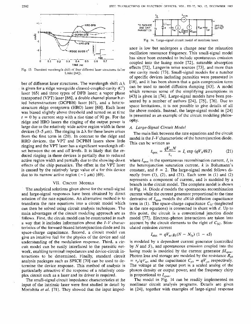
and large-signal responses have been obtained by direct solution of the rate equations. An alternative method is to transform the rate equations into a circuit model which can then be solved using circuit analysis techniques. The main advantages of the circuit modeling approach are a s follows. First, the circuit model can be constructed in such a way that it includes information about the I-I/ charac- teristics of the forward-biased heterojunction diode and its space-charge capacitance. Second, a circuit model can give an intuitive feel for the physics of the device and ;lid understanding of the modulation response. Third, a c,ir- cuit model can be easily interfaced to the parasitic net- work, enabling terminal impedances and device-circuit in- teractions to be determined. Finally, standard circuit analysis packages such as SPICE [70] can be used to de- termine the device response. This method of analysis is particularly attractive if the response of a relatively com- plex circuit such as a laser and its driver is required.
The small-signal circuit impedance characteristics at %e input of the intrinsic laser were first studied in detail b’y Morishita et al. [71]. They showed that the input imped-
TO PACKAGE AND CHIP
PARASITICS
OPTICAL
Fig. 14. Large-signal circuit model of instrinsic laser.
ance is low but undergoes a change near the relaxation oscillation resonance frequency. This small-signal model has since been extended to include spontaneous emission coupled into the lasing mode [72], saturable absorption effects [72], Langevin noise sources [73], and more than one cavity mode [73]. Small-signal models for a number of specific devices including parasitics were presented in [18], and it has been shown that a gain compression term can be used to model diffusion damping [43]. A model which removes some of the simplifying assumptions in [43] is given in [74]. Large-signal models have been pre- sented by a number of authors [24], [75], [76]. Due to space limitations, it is not possible to give details of all the above models. Instead, the large-signal model in [24] is presented as an example of the circuit modeling philos- ophy* A . Large-Signal Circuit Model
The main link between the rate equations and the circuit model is the I-Vcharacteristic of the heterojunction diode. This can be written as
where Ispon in the spontaneous recombination current, I, is the heterojunction saturation current, k is Boltzmann’s constant, and 8 2: 2. The large-signal model follows di- rectly from (l), (2), and (21). Each term in (1) and (2) represents a component of current, and is modeled by a branch in the circuit model. The complete model is shown in Fig. 14. Diode d models the spontaneous recombination current while the current generator proportional to the time derivative of Zspon models the diV/dt diffusion capacitance term in (1). The space-charge capacitance C,, (neglected in the rate equations) is connected in shunt with d. Up to this point, the circuit is a conventional junction diode model [77]. Electron-photon interactions are taken into account by the circuit elements to the right of Csc. Stim- ulated emission current
Istim = qvactgo ( N - NO^) (1 - E S ) is modeled by a dependent current generator (controlled by N and S), and spontaneous emission coupled into the lasing mode is modeled by the current generator PIspon. Photon loss and storage are modeled by the resistance Rph = rp/qVact and the capacitance c p h = qVact respectively. The voltage at the output port is a scaled analog of the photon density or output power, and the frequency chirp is proportional to IsPo,,.
The model in Fig. 14 can be readily implemented on nonlinear circuit analysis programs. Details are given in [24], together with examples of large-signal response
TUCKER: HIGH-SPEED MODULATION OF SEMICONDUCTOR LASERS
calculations. Small-signal circuit models of the type de- scribed in [18], [43], and [71]-[74] can be obtained di- rectly by linearizing a large-signal model of the type shown in Fig. 14 or by first linearizing (l), ( 2 ) , and (22), and then directly synthesizing the equivalent circuit.
VIII. CONCLUSIONS In the development of high-speed semiconductor lasers
it is necessary to solve a variety of device and circuit prob- lems. Electrical parasitics associated with the package and chip c;3n seriously degrade the modulation response at high frequencies and should be minimized when high-speed operation is required. The bandwidth of the intrinsic laser is controlled by the relaxation oscillation resonance fre- quency and associated damping mechanisms. Large band- width and a well damped response is achieved in narrow- stripe lasers with strong optical field confinement. The dominant damping mechanism appears to be spectral hole burning but more work is needed to improve understand- ing of the physical processes involved in damping. This is particularly true for applications where chirp is a problem. Nevertheless, there has been considerable recent progress in the development of low-parasitic structures with high resonance frequencies and it is expected that further im- provelments in high-speed performance will follow.
ACKNOWLEDGMENT The: author wishes to acknowledge useful and informa-
tive discussions with many of his colleagues, particularly J. E. lBowers, T. E. Darcie, G. Eisenstein, I. P. Kaminow, T. L. Koch, R. A. Linke, and D. J. Pope. He would also like to thank R. A. Linke for permission to use the exper- imental data in Fig. 13.
REFERENCES C . B. Su, V. Lanzisera, R. Olshansky, W. Powazinik, E. Meland, J. Schlafer, and R. B. Lauer, “15-GHz direct modulation bandwidth of valpor-phase regrown 1.3 pm InGaAsP buried-heterostructure lasers under cw operation at room temperature,” Electron. Lett., vol. 21, pp. 577-579, June 1985. J. E. Bowers, T. L. Koch, B. R. Hemenway, T. J. Bridges, E. G. Bnrkhardt, and D. P. Wilt, “8-GHz bandwidth 1.52 pm vapor phase transported InGaAsP lasers,” in Proc. OSA Conf Lasers and Elec- trooptics (Baltimore, MD), 1985, pp. 88-90. J. E. Bowers, B. R. Hemenway, A. H. Gnauck, T. J. Bridges, and E. G. Burkhardt, “High-frequency constricted mesa lasers,” Appl. Phys.
U. Koren, G. Eisenstein, J. E. Bowers, A. H. Gnauck, and P. K. Tien, “Wide-bandwidth modulation of three channel buried crescent laser dl~odes,” Electron. Lett., vol. 21, pp. 500-501, May 1985. P. J. Chidgey, E. R . White, N. (3. Brain, R. C. Hooper, D. R. Smith, P. P. Smyth, P. J. Fiddyment, A. W. Nelson, and L. D. Westbrook, “1.2 Gbis optical fiber transmission experiment over 113.7 km using a 1.528 Fm DFB ridge-waveguide laser,” Electron. Lett., vol. 20, pp.
J. Yamada, A. Kawana, H. Nagai, and T. Kimura, “1.55 Wm optical txansmission experiments at 2 Gbis using 51.5 km dispersion-free fi- ber,” EZectron. Lett., vol. 18, pp. 98-100, Jan. 1982. A. H. Gnauck, B. L. Kasper, R. A. Linke, R. W. Dawson, T. L. K.och, T. J. Bridges, E. G. Burkhardt, R. T. Yen, D. P. Wilt, J. C. Campbell, K. C. Nelson, and L. G. Cohen, “4 Gbis transmission over 103 km of optical fiber using a novel electronic multiplexeridemulti- plexer,” J. Lightwave Technol., vol. LT-3, Sept. 1985. J. J. Pan, “Microwave fiber-optic communications systems,” in Proc. IEEE Nut. Telecommunications Conf (New Orleans, LA), 1981, pp. C1.l.l-C1.1.8; also, W. E. Stephens and T. R. Joseph, “A 1.3-pm microwave fiber-optic link using a direct-modulated laser transmit- tar,” J. Lightwave Technol., vol. LT-3, pp. 308-315, Apr. 1985. R.. A. Kiehl and D. M. Drury, “Performance of optically coupled
Lstt., VOI. 47, pp. 78-80, July 1985.
707-709, Aug. 1984.
2583
VOI. MTT-29, pp. 1004-1010, Oct. 1981. microwave switching devices,” IEEE Trans. Microwave Theory Tech.,
[lo] J. R. Forrest and A. A . Salles, “Optics control microwaves,” Micro- wave Syst. News, vol. 11, no. 11, pp. 112-122, June 1981.
[ l l ] K. P. Jackson, S. A. Newton, B. Moslehi, M. Tur, C . C . Cutler, J. W. Goodman, and H. J. Shaw, “Optical fiber delay-line signal pro- cessing,’’ IEEE Trans. Microwave Theory Tenh . , vol. MTT-30, pp. 193-210, Mar. 1985.
[12] J. M. Osterwalder and B. J. Rickett, “Frequency modulation of GaAlAs injection lasers at microwave frequencies,” ZEEE J. Quantum Electron., vol. QE-16, pp. 250-252, Mar. 1980.
1131 T. Okoshi, “Heterodyne and coherent optical fiber communications: recent progress,” IEEE Trans. Microwave Theory Tech., vol. MTT- 30, pp. 1138-1149, Aug. 1982.
[14] T. L. Koch and J. E. Bowers. “Nature of wavelength chiming in di- - rectly modulated semiconductor lasers,” Electron. Lett., vol. 20, pp. 1038-1039, Dec. 1984. R. A. Linke, “Modulation induced transient chirping in single fre- quency lasers,” IEEE J. Quantum Electron., vol. QE-21, pp. 593- 597, June 1985. H. Kressel and J. K. Butler, Semiconductor Lasers and Heterojunc- tion LED’s. New York: Academic, 1977. Y. Okano, K. Nakagawa, and T. Ito, “Laser mode partition noise eval- uation for optical fiber transmission,” ZEEE Trans. Commun., vol.
R. S. Tucker and D. J. Pope, “Microwave circuit models of semicon- ductor injection lasers,” IEEE Trans. Microwuve Theory Tech., vol. MTT-31, pp. 289-294, Mar. 1983. I. Ury and K. Y. Lau, “Very high frequency GaAlAs laser field-effect transistor monolithic integrated circuit,” Appl. Phys. Lett., vol. 41, pp. 126-128, July 1982. H. Matsueda, S. Sasaki, and M. Nakamura, “GaAs optoelectronic integrated light sources,” J. Lightwave Technol., vol. LT-1, pp. 261- 269, Mar. 1983. K. Kishino, S. Aoki, and Y. Suematsu, “Wavelength variation of 1.6- pm wavelength buried heterostructure GaInAsPiInP lasers due to di- rect modulation,” ZEEE J Quantum Electron., vol. QE-18, pp. 343- 351, Mar. 1982. S. Kobayashi, Y. Yamamto, M. Ito, and T. Kimora, “Direct frequency modulation in AlGaAs semiconductor lasers,” I‘EEE J. Quantum Elec- tron., vol. QE-18, pp. 582-595, Apr. 1982. R. A. Linke, “Direct gigabit modulation of injection lasers: Structure dependent speed limitations,” J. Lightwave Technol. , vol. LT-2, pp. 40-43, Feb. 1984. R. S. Tucker and I. P. Kaminow, “High-frequency characteristics of directly modulated InGaAsP ridge waveguide and buried heterostruc- ture lasers,” J. Lightwave Technol., vol. LT-.2, pp. 385-393, Aug. 1984. I. D. Henning, “High-speed transient effects in quaternary lasers,” Proc. Znst. Elec. Eng., vol. 131, part H, pp. 133-138, June 1984. D. A. Frisch and I. D. Henning, “Effect of laser chirp on optical systems-Initial tests using a 1480 nm DFB laser,” Electron. Lett.,
T. Paoli, “Near-threshold behavior of the intrinsic resonant frequency in a semiconductor laser,” ZEEE J. Quantum Electron., vol. QE-15,
R. J. Nelson, R. B. Wilson, P. D. Wright, P. A. Barnes, and N. K. Dutta, “CW electrooptical properties of InGaAsP (X = 1.3 pm) bur- ied heterostructure lasers,” ZEEE J. Quantum Electron., vol. QE-17, pp. 202-207, 1981. N. K. Dutta, D. P. Wilt, and R. J. Nelson, “Analysis of leakage cur- rents in 1.3-pm InGaAsP real-index-guided lasers,” J. Lightwave Technol., vol. LT-2, pp. 201-208, June 1984. K. Y. Lau and A. Yariv, “Ultra-high speed liemiconductor lasers,” IEEE J. Quantum Electron., vol. QE-21, pp. 121-137, Feb. 1985. L. Figueroa, C. Slayman, and H. W. Yen, “High-frequency charac- teristics of GaAlAs injection lasers,” IEEE J. Quantum Electron.,
N. Bar-Chaim, J. Katz, I. Ury, and A. Yariv, “Buried heterostructure AlGaAs laser on semi-insulating substrate,” Electron. Lett., vol. 17,
G. Arnold, P. Russer, and K. Petermann, “Modulation of laser diodes,” in Semiconductor Devices for Optical Communication, H. Kressel, Ed. New York: Springer, 1980. P. M. Boers and M. T. Vlaardingerbroek, “Dynamic behavior of semiconductor lasers,” Electron. Lett., vol. 11, pp. 206-208, May 1975. N. Chinone, K. Aiki, M. Nakamura, and R. Ito, “Effects of lateral mode and carrier density profile on dynamic behaviors of semicon-
I -
COM-28, pp. 238-243, 1980.
V O ~ . 20, pp. 631-633, July 1984.
pp. 807-812, Aug. 1979.
VOI. QE-18, pp. 1718-1727, 1982.
pp. 108-109, 1981.
2584 IEEE TRANSACTIONS ON ELECTRON DEVICES, VOL. ED-32, NO. 12, DECEMBER 1985
ductor lasers,” IEEE J. Quantum Electron., vol. QE-14, pp. 625-631, Aug. 1978.
[36] K. Furuya, Y. Suematsu, and T. Hong, “Reduction of resonance-like peak in direct modulation due to carrier diffusion in injection lasers,” Appl. Opt., vol. 17, pp, 1949-1952, June 1978.
[37] G. H. B. Thompson, Physics of Semiconductor Laser Devices, New York: Wiley, 1980. D. J. Channin, “Effect of gain saturation on injection laser switch- ing,’’ 1 Appl. Phys., vol. 50, pp. 3858-3860, June 1979; als3, M. Yamada and T. Mizukami, “An analysis of direct modulation :n un- doped injection laser with consideration of inhomogeneous gain broadening,” Trans. IECE of Japan, vol. E63, pp. 795-802, Nov. 1980. M. Asada and Y . Suematsu, “Density-matrix theory of semiconciuctor lasers with relaxation broadening model-gain and gain-supprc ssion in semiconductor lasers,” IEEE J. Quantum Electron., vol. QE-21, pp. 434-442, May 1985. M. J. Adams and M. Osinski, “Influence of spectral hole-burni:lg on quaternary laser transients,” Electron. Lett., vol. 19, pp. 627--628, 1983. J. Manning, R. Olshansky, D. M. Fye, and W. Powazinik, “S:rong influence of nonlinear gain on spectral and dynamic characterist ICS of InGaAsP lasers,” Electron. Lett., vol. 21, pp. 496-497, May 1985. 3. E. Bowers, T. L. Koch, B. R. Hemenway, P. D. Wilt, T. J. Bridges, and E. G. Burkhardt, “High frequency modulation of 1.52 pm vlpor- phase-transported InGaAsP lasers,” Electron. Lett., vol. 21, pp. 297- 299, Mar. 1985. R. S. Tucker and D. J. Pope, “Circuit modeling of the effects o ’ dif- fusion damping in a narrow-stripe semiconductor laser,” IEFE J. Quantum Electron., vol. QE-19, pp. 1179-1183, July 1983. K. Y. Lau, N. Bar-Chaim, I. Ury, Ch. Harder, and A. Yariv, “Cirect amplitude modulation of short-cavity GaAs lasers up to X-band fre- quencies,” Appl. Phys. Lett., vol. 43, pp. 1-3, July 1983. F. F Kuo, Network Analysis and Synthesis, 2nd ed. New York: Wiley, 1966. B. S . Poh, “Prediction of self-sustained oscillations in buried-hster- ostructure stripe lasers,” Proc. Inst. Elec. Eng., vol. 132, Part I , pp. 29-33, Feb. 1985. K. Y. Lau, N. Bar-Chaim, I . Ury, and A. Yariv, “An 11-GHz direct modulation bandwidth GaAlAs window laser on semi-insulating sub- strate operating at room temperature,” Appl. Phys. Lett., vol. 45, pp.
C. B. Su and V. Lanzisera, “Effect of doping level on the gain con- stant and modulation bandwidth of InGaAsP semiconductor lasers,” Appl. Phys. Lett., vol. 45, pp. 1302-1304, Dec. 1984. Y. Arakawa, K. Vahala, and A. Yariv, “Quantum noise and dyna:nxs in quantum well and quantum wire lasers,” Appl. Phys. Lett., vol.
R. S. Tucker, Chinlon Lin, C. A. Burrus, P. Besomi, and R. J. Nel- son, “High-frequency small-signal modulation characteristics of short- cavity InGaAsP lasers,” Electron. Lett., vol. 20, pp. 393-394, May 1984. T. L. Koch and J. E. Bowers, “Factors affecting wavelength chirping in directly modulated semiconductor lasers,” in Proc. Con$ Layers and Electrooptics (Baltimore, MD), May 1985, pp. 72-74. G. P. Agrawal, “Coupled-cavity semiconductor lasers under current modulation: Small-signal analysis,” IEEE J. Quantum Electron., vol. QE-21, pp. 255-263, Mar. 1985. C. H. Henry, “Theory of the linewidth of semiconductor lasers,” IEEE J. Quantum Electron., vol. QE-18, pp. 259-264, Feb. 1982. J. E. Bowers, W. T. Tsang, T. L. Koch, N. A. Olsson, and R. A . Logan, “Microwave intensity and frequency modulation of hetcro- epitaxial-ridge-overgrown distributed-feedback lasers,” Appl. Phys. Lett., vol. 46, pp. 233-235, Feb. 1985. T. Ikegami and Y. Suematsu, “Large-signal characteristics of dire,t(y modulated semiconductor injection lasers,” Elec. Commun. Japan,
T. Hong, Y. Suematsu, S . Chung, and M. Kang, “Harmonic cha’ac- teristics of laser diodes,” J. Optical Commun., vol. 3, pp. 42-48, 1982. H. Grothe and W. Harth, ,,“Experimental investigation of parametric sideband amplification in injection lasers,” Electron Lett., vol. 12, pp. 522-524, Sept. 1975. G. J. Aspin and J. E. Carroll, “Gain-switched pulse generation with semiconductor lasers,” Proc. Inst. Elec. Eng., vol. 129, Part I, pp.
M. S . Demokan and A. Nacaroglu, “An analysis of gain-switched semiconductor lasers generating pulse-code-modulated light wit I a
316-318, Aug. 1984.
45, pp. 950-952, NOV. 1984.
V O ~ . 53-B, pp. 69-75, 1970.
283-290, 1982.
high bit rate,” IEEE J. Quantum Electron., vol. QE-20, pp. 1016- 1022, Sept. 1984. R. S . Tucker, “Large-signal switching transients in index-guided semiconductor lasers,” Electron. Lett., vol. 20, pp. 802-803, Sept. 1984. D . J . Channin, D. Botez, C. C. Neil, J. C. Connolly, and D. W. Bechtle, “Modulation characteristics of constricted double-hetero- junction AlGaAs laser diodes,” J. Lightwave Technol., vol. LT-1, pp. 146-160, Mar. 1983. R. Olshansky and D . Fye, “Reduction of dynamic linewidth in single- frequency semiconductor lasers,” Electron. Lett., vol. 20, pp. 928- 929, 1984. L. Bickers and L. D. Westbrook, “Reduction of laser chilp in 1.5-ym DFB lasers by modulation pulse shaping,” Electron. Lett., vol. 21, pp. 103-104, Jan. 1985. R. A. Linke, “High-capacity single-frequency laser transmission sys- tems,’’ presented at Conf. Optical Fiber Communication, San Diego, CA, Feb. 1985. I . P. Kaminow, J.-S. KO R. A. Linke, and L. W. Stulz, “High-speed 1.55-pm single-longitudinal mode ridge waveguide laser,” Electron. Lett., vol. 19, pp. 784-785, 1983. T. L. Koch, T. J . Bridges, E. G. Burkhardt, P. J. Corvini, L. A. Coldren, R. A. Linke, W. T. Tsang, R. A. Logan, L. F. Johnson, R. F. Kazarinov, R. Yen, and D. P. Wilt, “1.55-ym InGaAsP distributed feedback vapor phase transported buried heterostructure lasers,” Appl. Phys. Lett., vol. 47, pp. 12-14, July 1985. I. Mito, M. Kitamura, K. Kobayashi, S . Murata, M. Seki, Y. Odagiri, H. Nishimoto, M. Yamaguchi, and K. Kobayashi, “InGaAsP double channel planar buried heterostructure laser diode (DCPBH LD) with effective current confinement,” J. Lightwave Technol., vol. LT-1, pp. 195-202, Mar. 1983. W. T. Tsang, N. A. Olsson, R. A. Logan, C. H. Henry, L. F. John- son, J. E. Bowers, and J. Long, “The heteroepitaxial ridge-overgrown distributed feedback laser,” IEEEJ. Quantum Electron., vol. QE-21, pp. 519-526, June 1985. T. L. Koch and R. A. Linke, to be published. L. W. Nagel, “SPICE2: a computer program to simulate semiconduc- tor circuits,” Electronics Research Laboratory, Univ. of California, Berkeley, CA, Rep. ERL-M520, 1975. M. Morishita, T. Ohmi, and J.-I. Nishizawa, “Impedance character- istics of double-heterostructure laser diodes,” Solid-State Electron.,
J. Katz, S. Margalit, C . Harder, D. Wilt, and A. Yariv, “The intrinsic electrical equivalent circuit of a laser diode,” IEEE J. Quantum Elec- tron., vol. QE-17, pp. 4-7, Jan. 1981. C. Harder, J. Katz, S . Margalit, J. Shacham, and A. Yariv, “Noise equivalent circuit of a semiconductor laser diode,” IEEE J. Quantum Electron., vol. QE-18, pp. 333-337, Mar. 1982. W. W. Ng and E. A. Sovero, “An analytic model for the modulation response of buried heterostructure lasers,” IEEE J. Quantum Elec- tron., vol. QE-20, pp. 1008-1015, Sept. 1984. I. Habermayer, “Nonlinear circuit model for semiconductor lasers,” Optical and Quantum Electron., vol. 13, pp. 461-468, 1981. R. S . Tucker, “Large-signal circuit model for simulation of injection- laser modulation dynamics,” Proc. Inst. Elec. Eng., vol. 128, Part I,
S. M. Sze, Physics of Semiconductor Devices, 2nd ed., New York: Wiley, 1981.
V O ~ . 22, pp. 951-962, 1979.
pp. 180-184, Oct. 1981.
1