on the consistent choice of effective permittivity and
TRANSCRIPT

Research Article Vol. 38, No. 10 / October 2021 / Journal of the Optical Society of America A 1511
On the consistent choice of effective permittivityand conductivity for modeling grapheneYoungjoon Hong1 AND David P. Nicholls2,*1Department ofMathematics, SungkyunkwanUniversity, Suwon 440-746, Republic of Korea2Department ofMathematics, Statistics, andComputer Science, University of Illinois at Chicago, Chicago, Illinois 60607, USA*Corresponding author: [email protected]
Received 28 April 2021; revised 16 August 2021; accepted 19 August 2021; posted 20 August 2021 (Doc. ID 430088);published 23 September 2021
Graphene has transformed the fields of plasmonics and photonics, and become an indispensable component fordevices operating in the terahertz to mid-infrared range. Here, for instance, graphene surface plasmons can beexcited, and their extreme interfacial confinement makes them vastly effective for sensing and detection. The rapid,robust, and accurate numerical simulation of optical devices featuring graphene is of paramount importance andmany groups appeal to Black-Box Finite Element solvers. While accurate, these are quite computationally expen-sive for problems with simplifying geometrical features such as multiple homogeneous layers, which can be recastin terms of interfacial (rather than volumetric) unknowns. In either case, an important modeling considerationis whether to treat the graphene as a material of small (but non-zero) thickness with an effective permittivity, oras a vanishingly thin sheet of current with an effective conductivity. In this contribution we ponder the correctrelationship between the effective conductivity and permittivity of graphene, and propose a new relation which isbased upon a concrete mathematical calculation that appears to be missing in the literature. We then test our newmodel both in the case in which the interface deformation is non-trivial, and when there are two layers of graphenewith non-flat interfacial deformation. © 2021 Optical Society of America
https://doi.org/10.1364/JOSAA.430088
1. INTRODUCTION
Graphene, a sheet of carbon atoms in a honeycomb lattice, hastransformed the fields of plasmonics and photonics with itsblend of remarkable mechanical, chemical, and electronic prop-erties [1]. First isolated experimentally in 2004, resulting in theawarding of the 2010 Nobel Prize to Geim [2] and Novelsolov[3], graphene has become indispensable for devices operatingin the terahertz to mid-infrared range where graphene surfaceplasmons (GSPs) can be excited [4]. The extreme interfacialconfinement of these GSPs renders them vastly effective forsensing and detection. Recent work on graphene and othertwo-dimensional materials can be found in [5–8] while surveyarticles [9–13] describe the use of graphene in engineeringdevices.
From these considerations, it is clear that the rapid, robust,and accurate numerical simulation of optical devices featuringgraphene is of paramount importance. Most engineering groupsappeal to Black-Box Finite Element solvers such as COMSOLMultiphysics [14], e.g., [8,15], and a general overview ofnumerical methods for plasmonics problems can be foundin the survey paper of Gallinet et al. [16]. While such simula-tions provide accurate solutions, they are typically exceedinglycomputationally expensive for problems with simplifying geo-metrical features. For instance, diffraction grating structures
with multiple homogeneous layers can be modeled with sys-tems of differential equations featuring interfacial (rather thanvolumetric) unknowns, see, e.g., [17]. It was recently shownhow such formulations can be extended to the case where two-dimensional materials are present [18,19] and these materialsare modeled as vanishingly thin sheets of current with an effectiveconductivity. This approach has been adopted by several othergroups, and we point to the surveys [20,21] and the recent workof [11,22–25].
However, an alternative approach which fits much morenaturally into the framework of standard FEMs is to modelthe graphene as a thin layer of finite (but small) thickness withan effective permittivity. The question we entertain in thiscontribution is the correct relationship between the (non-dimensionalized) effective conductivity, σ (g ), and effectivepermittivity, ε(g ), of graphene. The relationship given in[11,22] is
σ (g ) =k0dg ε
(g )
i, (1)
where dg is the graphene layer thickness (reported in [11,22] as0.34 nm) and k0 =ω/c 0 is the free-space wavenumber. In thispaper, we propose a new relation
1084-7529/21/101511-10 Journal © 2021 Optica Publishing Group

1512 Vol. 38, No. 10 / October 2021 / Journal of the Optical Society of America A Research Article
σ (g ) =k0dg E (h)
i, (2)
where E (h) is given in Eq. (10),
limh→0
E (h)= E0 := ε(g )+
√ε(w)
2
(√ε(u) −
√
ε(w)),
h = dg /2, and ε(u) and ε(w) are permittivities of the mountingstructure above and below, respectively, the graphene sheet.As we shall show, this is based upon a concrete mathematicalcalculation which appears to be missing in the literature. Forthis, we make several simplifying assumptions to make progresswith our rather explicit calculations. More specifically, we matchthese two approaches in the case of normal incidence and a flatinterface between the dielectrics which mount the graphenesheet. We then test our results more fully in the case where theinterface deformation is non-trivial in order to assess the utilityof our formula for the effective conductivity. Such a compari-son is of vital importance, as corrugated gratings are one of theprincipal mechanisms for generating graphene surface plasmons(GSPs) [21,26].
The organization of the paper is as follows: In Section 2, werecall the governing equations, first for a triply layered mediumin Section 2.A and then for a doubly layered medium with aninterfacial current in Section 2.B. In Section 3, we derive a morefaithful formula for the effective conductivity in terms of thepermittivity of graphene, while in Section 3.A we report a stand-ard Drude model for this permittivity. In Section 4, we discussthe outcomes of our numerical simulations, with a descriptionof our numerical methods in Section 4.A and a full commentaryon figures which summarize our discoveries in Section 4.B,more specifically for a single graphene sheet in Section 4.C and adouble sheet configuration in Section 4.D.
2. GOVERNING EQUATIONS
We consider the simplest possible configurations to connect theeffective permittivity of graphene and its effective conductivity:A triply layered medium and a doubly layered structure with aninterfacial current (see Fig. 1).
We begin with the case of flat interfaces, but later in the paperwe will test the integrity of our calculations by considering thesame structures with periodically corrugated interfaces. We nowdiscuss each of these two models.
A. Triply Layered Medium
For the triply layered configuration, we consider y -invariant,periodically corrugated interfaces at z= h + g (x ), g (x + d)=g (x ), and z=−h + `(x ), `(x + d)= `(x ). These determinethree domains,
S(u) = {z> h + g (x )}, S(w) = {z<−h + `(x )},
S(v) = {−h + `(x ) < z< h + g (x )},
filled with materials of permittivities {ε(u), ε(v), ε(w)}. Thestructure is illuminated by transversely polarized, monochro-matic, plane-wave incidence of frequency ω and wavenumberk(u) =
√ε(u)k0,
0 0.2 0.4 0.6 0.8 1-2
-1.5
-1
-0.5
0
0.5
1
1.5
2
Fig. 1. Plot of the structure under consideration: graphenemounted on dielectric under vacuum. Structure rescaled by theperiod in the x coordinate and the maximum amplitude in the zcoordinate.
u inc(x , z)= e iαx−iγ (u)z, α = k(u) sin(θ), γ (u) = k(u) cos(θ).
It is not difficult to see that the governing equations for thescattered transverse components of the fields in each layer,{u, v, w}, are [27]
1u + ε(u)k20u = 0, in S(u), (3a)
1v + ε(v)k20v = 0, in S(v), (3b)
1w+ ε(w)k20w= 0, in S(w), (3c)
u − v = ξ, z= h + g (x ), (3d)
τ (u)∂Nu − τ (v)∂Nv = τ(u)ν, z= h + g (x ), (3e)
v −w= 0, z=−h + `(x ), (3f)
τ (v)∂Nv − τ(w)∂Nw= 0, z=−h + `(x ). (3g)
In these, ∂N denotes the normal derivative ∂N = N · ∇ and
τ (m) =
{1, Transverse Electric (TE),
1/ε(m), Transverse Magnetic (TM),
where m ∈ {u, v, w}. It is understood that solutions arequasiperiodic, and that u and w are upward and downwardpropagating, respectively.
We now focus on the case of flat interfaces and normal inci-dence (θ = 0), and recall that the Rayleigh expansions [27] giveupward/downward propagating quasiperiodic solutions to thisproblem of the form
u =∞∑
p=−∞
a p e iαp x+iγ (u)p (z−h), (4a)
Research Article Vol. 38, No. 10 / October 2021 / Journal of the Optical Society of America A 1513
w=
∞∑p=−∞
d p e iαp x−iγ (w)p (z+h), (4b)
v =
∞∑p=−∞
b p
sin(γ (v)p (h + z)
)sin(
2γ (v)p h) + c p
sin(γ (v)p (h − z)
)sin(
2γ (v)p h)
e iαp x ,
(4c)whereαp = α + 2π p/d = 2π p/d and
γ (m)p =
√ε(m)k2
0 − α2p =
√ε(m)k2
0 −
(2π p
d
)2
, m ∈ {u, v, w}.
Now, Eqs. (3d)–(3g) imply 1 −1 0 0−G p −Hp −K p 0
0 0 1 −10 −K p −Hp −J p
a p
b p
c p
d p
=
ξp
τ (u)νp
00
,where
G p :=−τ(u)iγ (u)p , J p :=−τ
(w)iγ (w)p ,
Hp := τ(v)γ (v)p cot(γ (v)p 2h), K p :=−τ
(v)γ (v)p csc(γ (v)p 2h),
and
ξp =1
d
∫ d
0ξ(x )e−iαp x dx , νp =
1
d
∫ d
0ν(x )e−iαp x dx .
In the flat-interface, normal incidence case, the datawill be ξ =−1 and ν = (iγ (u)) so that ξp =−1δp,0 andνp = (iγ (u))δp,0, and only the specular wavenumber, p = 0,is excited. Here, δp,q is the Kronecker delta. With this, andmultiplying the second and fourth equations by−1, we find 1 −1 0 0
G0 H0 K0 00 0 1 −10 K0 H0 J0
a0
b0
c 0
d0
=
ξ0
−τ (u)ν0
00
.
The first and third equations give
a0 = b0 + ξ0, c 0 = d0,
which simplify the remaining equations to(G0 + H0 K0
K0 H0 + J0
)(b0
d0
)=
(−G0ξ0 − τ
(u)ν0
0
).
For future use, we can solve for the Fourier coefficient of thetransmitted wave
d0 =
−K0
(−τ (u)ν0 − G0ξ0
)(G0 + H0) (H0 + J0)− K 2
0
. (5)
B. Doubly Layered Medium
As we demonstrated in [18], for a flat interface configuration atz= 0, the equations for a doubly layered medium with an inter-facial current with non-dimensional conductivity σ (g ) are
u −w+ P τ (w)∂zw= ξ, z= 0, (6a)
τ (u)∂zu − τ (w)∂zw+ Sw= τ (u)ν, z= 0, (6b)
where
S ={
ik0σ(g ), TE,
0, TM,P =
{0, TE,
σ (g )/(ik0), TM.
Appealing to the (rescaled) Rayleigh expansions
u = u(x , z)=∞∑
p=−∞
a p e iαp x+iγ (u)p z, (7a)
w=w(x , z)=∞∑
p=−∞
d p e iαp x−iγ (w)p z, (7b)
cf. Eq. (4), the governing equations, Eq. (6), imply(1 −1+ P J p
−G p −J p + S
)(a p
d p
)=
(ξp
τ (u)νp
).
As above, we note that only the specular wavenumber, p = 0, isexcited so that the governing equations simplify to(
1 −1+ P J0
−G0 −J0 + S
)(a0
d0
)=
(ξ0
τ (u)ν0
),
or, multiplying the second equation by−1, we have(1 −1+ P J0
G0 J0 − S
)(a0
d0
)=
(ξ0
−τ (u)ν0
).
From this, we find that the solution for the Fourier coefficient ofthe transmitted wave is
d0 =−G0ξ0 − τ
(u)ν0
G0 + J0 − S − P G0 J0. (8)
3. EFFECTIVE CURRENT
If the relationship between σ (g ) and ε(g ) [e.g., Eq. (1) or Eq. (2)]is to be consistent, then the d0 from Eq. (5) must be correctlyrelated to d0 from Eq. (8). At this point, we specialize the calcu-lations of Section A to that of a sheet of graphene of thicknessh = dg /2 and permittivity ε(v) = ε(g ). We make our resultsprecise in the fundamental result of this paper.Theorem 3.1. For d0 from Eq. (5) to be consistent with d0 fromEq. (8), we must have the relation
σ (g ) =k0dg E (h)
i, (9a)
where
E (h)=�(h) sinc(√ε(g )k02h
) (ε(g ) +
√
ε(u)ε(w))
− B(h)
(√ε(u)ε(w) + ε(w)
)2
, (9b)

1514 Vol. 38, No. 10 / October 2021 / Journal of the Optical Society of America A Research Article
B(h)=�(h) cos
(√ε(g )k02h
)− 1
i√ε(w)k0h
, (9c)
�(h)= exp(iγ (w)h), (9d)
and
limh→0
E (h)= E0 = ε(g )+
√ε(w)
2
(√ε(u) −
√
ε(w))
.
Proof. We begin by finding the consistent relationshipbetween d0 and d0. For this, we evaluatew at z=−h in Eqs. (4)and (7), respectively:
w(x ,−h)=∞∑
p=−∞
d p e iαp x e−iγ (w)p (−h+h)= d0e iαx ,
w(x ,−h)=∞∑
p=−∞
d p e iαp x e−iγ (w)p (−h)= d0e iαx e iγ (w)h ,
so that
d0 = d0e iγ (w)h= d0�.
With this, Eqs. (5) and (8) demand that
�
(−G0ξ0 − τ
(u)ν0
G0 + J0 − S − P G0 J0
)=�d0
= d0 =
−K0
(−τ (u)ν0 − G0ξ0
)(G0 + H0) (H0 + J0)− K 2
0
,
which demands that
�{(G0 + H0)(H0 + J0)− K 2
0
}=−K0 {G0 + J0 − S − P G0 J0} .
We point out that the incident data, {ξ, ν}, cancel out in thiscalculation which does not occur if one attempts to reconcile a0
with a0.Using the fact that
H20 − K 2
0 =(τ (g )
)2(γ (g )
)2 {cot2 (γ (g )2h
)− csc2 (γ (g )2h
)}=−(τ (g ))2(γ (g ))2
=:−02,
which is independent of h , we have
�{−02+ G0 J0 + G0 H0 + H0 J0
}=−K0 {G0 + J0 − S − P G0 J0} .
Solving for the terms involving the current, S and P , we find
S + G0 J0 P = Q + R,
where
Q := K −10 �
{−02+ G0 J0
},
R := (I + K −10 �H0)(G0 + J0).
We begin our study of these functions by noting the followingthree facts. First,
K −10 =
1
−τ (g )γ (g ) csc(γ (g )2h
)=−
(2hτ (g )
){sin(γ (g )2h
)γ (g )2h
}
=−
(2hτ (g )
)sinc
(γ (g )2h
),
where sinc(z)= sin(z)/z=O(1) as z→ 0. Next,
K −10 H0 =− cos
(γ (g )2h
).
Finally, normal incidence (θ = 0) givesα = 0 and
γ (m) =√
ε(m)k0.
We now focus upon Q:
Q =−(
2hτ (g )
)sinc
(γ (g )2h
)�(h)
×
(−(τ (g )
)2(γ (g )
)2− τ (u)γ (u)τ (w)γ (w)
)= 2hk2
0 sinc(√ε(g )k02h
)�(h)E Q,
where
E Q := τ(g )ε(g ) +
τ (u)τ (w)
τ (g )
√
ε(u)ε(w).
Moving to R , we have
R =(�(h)K −1
0 H0 + 1)(G0 + J0)
= iγ (w)h
(−�(h) cos
(γ (g )2h
)+ 1
iγ (w)h
)×(τ (u)
(−iγ (u)
)+ τ (w)
(−iγ (w)
))=−hk2
0 B(h)E R ,
where
E R := τ(u)√
ε(u)ε(w) + τ (w)ε(w).
While B depends upon h , it is not difficult to show that B isO(1) as h→ 0 since
B(h)=�(h) cos
(γ (g )2h
)− 1
iγ (w)h
=
(1+ iγ (w)h +O
(h2)) (
1+O(h2))− 1
iγ (w)h
=i√ε(w)k0h +O
(h2)
i√ε(w)k0h
= 1+O(h).

Research Article Vol. 38, No. 10 / October 2021 / Journal of the Optical Society of America A 1515
So from this, we learn that
S + G0 J0 P = 2hk20 E (h),
where
E (h) :={�(h) sinc
(√ε(g )2hk0
)E Q − B(h)
E R
2
}. (10)
We have two polarizations to consider and we note that only{E Q, E R} depend upon this. In Transverse Electric (TE), wefind
E TEQ = ε
(g )+
√
ε(u)ε(w), E TER =√
ε(u)ε(w) + ε(w),
while in Transverse Magnetic (TM) polarization we have
E TMQ = 1+
ε(g )√ε(u)ε(w)
, E TMR =
√ε(w)√ε(u)+ 1.
However, straightforward simplification of the previous formu-lae yields
E TMQ =
E TEQ
√ε(u)ε(w)
, E TMR =
E TER
√ε(u)ε(w)
.
Now, in TE polarization, we have P = 0 so that
σ (g ) =S
ik0=(2h)k0
iE (h)=
k0dg
iE (h), (11)
where dg = 2h . Meanwhile, in TM polarization, using S = 0,we find
σ (g ) = ik0 P =ik0ε
(u)ε(w)(−i√ε(u)k0
) (−i√ε(w)k0
) (2hk20
)E (h)
=(2h)k0
iE (h)=
k0dg
iE (h),
and we find a single function E (h)which can be used to define aconsistent effective current that works for both polarizations.
Finally, using the fact that {�(h), B(h), sinc(γ (v)h)} =O(1) as h→ 0, we see that the small-thickness limit of σ (g ) is
σ(g )0 =
(2h)k0
iE0 =
k0dg
iE0, (12)
where
E0 = ε(g )+
√
ε(u)ε(w) −
√ε(u)ε(w)
2−ε(w)
2
= ε(g ) +
√ε(u)ε(w)
2−ε(w)
2
= ε(g ) +
√ε(w)
2
(√ε(u) −
√
ε(w))
.
�
A. Effective Permittivity of Graphene
Now, we turn to our central purpose: the modeling of graphene.The faithful approximation of the electromagnetic response of
graphene is still a subject of ongoing research [21]. We employ asimple nondimensionalized Drude model which, from [11,22],gives the effective permittivity
ε(g ) =i σD
k0dg=
(i
k0dg
)(σ0
ε0c 0
)(4E F
π
)1
~γ − i~ω, (13)
where ~ is the reduced Planck’s constant, ω is the angular fre-quency, γ is the relaxation rate, and E F is the (local) Fermi levelposition. We point out that [11,22] asks for an effective currentof graphene,
σ (g ) =k0dg ε
(g )
i,
cf. Eq. (1), which matches our asymptotic model, Eq. (2), whenε(u) = ε(w) as E0 equals ε(g ) in this instance. We now investigatethe results of simulations with our bulk simulations of Eq. (3)against the interfacial current model, Eq. (6), with σ (g ) chosenamong the “unmodified” current, Eq. (1); the “asymptotic”model, Eq. (12); and the “full” current, Eq. (11).
4. NUMERICAL SIMULATIONS
In this section, we compare the simulation of sheets of cor-rugated graphene by the two approaches we outlined in theIntroduction: (i) As a thin layer of small, but non-zero, thicknesswith an effective permittivity ε(g ) from Eq. (13), and (ii) as aninterfacial layer of current with effective conductivity σ (g ) cho-sen from the “unmodified” current [Eq. (1)], the “asymptotic”model [Eq. (12)], and the “full” current [Eq. (11)].
A. Numerical Methods
The numerical algorithms we employ for our comparisonshave already been described in the literature, more specifically[28,29] for the triply layered configuration and [30,31] in thecase of a doubly layered structure with an interfacial current. Wenow briefly recall each of these and refer the interested reader tothe papers listed for complete details.
Regarding the triply layered model, the authors [28,29]describe a high-order spectral approach applied to a transformedfield expansion (TFE) restatement of the governing equations,Eq. (3), supplemented with Padé approximation techniques.In summary, a change of variables is effected which maps theperturbed geometry {z= h + g (x ), z=−h + `(x )} to thetrivial flat-interface one, {z′ = h, z′ =−h}, resulting in newdependent variables, {u(x ′, z′), v(x ′, z′), w(x ′, z′)} whichsatisfy inhomogeneous versions of Eq. (3). Importantly, the inho-mogeneities areO(g ) andO(`), which suggests that a boundaryperturbation approach, e.g., setting,
g (x )= εg (x ), `(x )= ε ˜(x ),{
g , ˜}=O(1), ε� 1,
will be fruitful. We point out that g and ˜ are dimensionlessso that ε has the same units as g and ` (e.g., micrometers).Experience has demonstrated the superior performance of theTFE method built upon the expansions
{u, v, w}(x ′, z′; ε
)=
∞∑n=0
{un, vn, wn}(x ′, z′
)εn,

1516 Vol. 38, No. 10 / October 2021 / Journal of the Optical Society of America A Research Article
and numerical simulation of the resulting recursively definedproblems for {un, vn, wn}. This is accomplished via aFourier/Legendre Galerkin method based upon forms like
un(x ′, z′)=Nx /2−1∑
p=−Nx /2
Nz∑q=0
u p,q e iαp x ′Lq(z′/h
),
where Lq (z) is the q -th Legendre function. Based upon rig-orous demonstration [32,33], the smallness assumption on εcan be dropped if it is chosen to be real . This observation canbe realized in numerical simulation with the use of numericalanalytical continuation algorithms such as Padé approximation[34] which we use here. This approach we denote the “bulk”simulation of Eq. (3), and we treat it as an exact solution.
Regarding the doubly layered simulations with interfacialgraphene, we utilized the scheme of one of the authors [30,31].Here a somewhat different approach is used where the volumet-ric problem is restated in terms of interfacial quantities, namelythe surface impedances. For instance, following the approach ofDespres [35,36], one defines
U(x ) := [−∂zu + iηu]z=g (x ), U(x ) := [−∂zu − iηu]z=g (x ),
W(x ) := [∂zw− iηw]z=g (x ), W(x ) := [∂zw+ iηw]z=g (x ),
for some η ∈R+ and rewrites the boundary conditions atz= g (x ) in Eq. (6) in terms of these, with the understand-ing that {u, w} satisfy the relevant Helmholtz equations andboundary conditions. At this point, we make the BoundaryPerturbation assumption
g (x )= εg (x ), g =O(1), ε� 1,
and expand the impedances in Taylor series{U , U ,W, W
}(x ; ε)=
∞∑n=0
{Un, Un,Wn, Wn
}(x )εn .
Insertion of these into the boundary conditions delivers arecursively defined sequence of problems (as in the previouslyshown TFE approach); however, these need only be enforcedat the interface, z= g (x ). The numerical method is a Fouriercollocation approach using representations of the form
U(x )=Nx /2−1∑
p=−Nx /2
Up e iαp x .
As with the TFE method, we avail ourselves of the beneficialproperties of numerical analytical continuation via the Padéapproximation algorithm [34]. We make three simulationswith this approach; the first is “unmodified” [with σ (g ) givenby Eq. (1)], the second is “asymptotic” [with σ (g ) specified byEq. (12)], and the third is “full” [with σ (g ) defined by Eq. (11)].
B. Numerical Results
In order to assess the performance of our effective conductivi-ties, we study the transmission of our configurations. For this,we recall the Rayleigh expansions, Eq. (7), and the definitions ofthe efficiencies [27]
e (u)p =γ (u)p
γ (u)
∣∣a p
∣∣2, e (w)p =γ (w)p
γ (u)
∣∣∣d p
∣∣∣2.
From this, we can define the reflection and transmission,
R =∑p∈U
e (u)p , T =∑p∈W
e (w)p , (14)
where U and W are the propagating modes in the upper andlower layers, respectively. As our derivation was based uponmatching the transmissions (in the flat-interface case), this is thequantity of interest upon which we focus.
In order to most effectively study the performance of ourmethod, we chose a configuration where the difference betweenthe response of flat-interface and non-flat-interface geometriesis maximized. Such an instance can be found at a GSP where asignificant enhancement in the scattered field can be found in asmall neighborhood of the layer interfaces. In [31] [Fig. 6(b)],we found that a particular double-layer graphene structuregenerated GSPs at the energies 11 and 26 meV, which we singleout for study in the following sections.
C. Single-Layer Graphene
We began with a configuration featuring a single layer ofgraphene between two dielectrics (with permittivities ε(u) andε(w)) mounted on the corrugated interface between the twolayers (shaped by z= g (x )= εg (x )), where
ε(u) = 1, ε(w) = 11, g (x )= cos(2π x/d),
d = 10, 0≤ ε≤ 0.4. (15)
We began with low-energy illumination at E = 11 meV(corresponding to λ≈ 112.7129 µm) and display results of thetransmission in Fig. 2 as computed by simulation of the “bulk”three-layer problem, and the two-layer configurations withconductivities specified by the “unmodified,” “asymptotic,”and “full” models specified previously. In addition, in Fig. 3,we show the difference between these latter three and the bulksimulation which we consider exact:
0 0.05 0.1 0.15 0.2 0.25 0.3 0.35 0.40.57
0.575
0.58
0.585
0.59
0.595
0.6
Fig. 2. Transmission from a single-sheet graphene configuration,Eq. (15), at E = 11 meV as computed by simulation of the “bulk”three-layer configuration, Eq. (3), and the two-layer structures withinterfacial currents which are “unmodified” [with σ (g ) given byEq. (1)], “asymptotic” [with σ (g ) specified by Eq. (12)], and “full”[with σ (g ) defined by Eq. (11)].

Research Article Vol. 38, No. 10 / October 2021 / Journal of the Optical Society of America A 1517
0 0.05 0.1 0.15 0.2 0.25 0.3 0.35 0.410-15
10-10
10-5
100
Fig. 3. Differences in transmission from a single-sheet grapheneconfiguration, Eq. (15), at E = 11 meV between a simulation of the“bulk” three-layer configuration, Eq. (3), and the two-layer structureswith interfacial currents which are “unmodified” [with σ (g ) given byEq. (1)], “asymptotic” [with σ (g ) specified by Eq. (12)], and “full”[with σ (g ) defined by Eq. (11)].
0 0.05 0.1 0.15 0.2 0.25 0.3 0.35 0.40.686
0.687
0.688
0.689
0.69
0.691
0.692
0.693
Fig. 4. Transmission from a single-sheet graphene configuration,Eq. (15), at E = 26 meV as computed by simulation of the “bulk”three-layer configuration, Eq. (3), and the two-layer structures withinterfacial currents which are “unmodified” [with σ (g ) given byEq. (1)], “asymptotic” [with σ (g ) specified by Eq. (12)], and “full”[with σ (g ) defined by Eq. (11)].
1T := |T − Tbulk| .
Remark 4.1. Here we can clearly see that, while all three modelsdo provide useful (at least moderately accurate) answers, the“full” model that we advocate provides the best results for smallvalues of ε (0≤ ε≤ 0.025) being exact to machine precisionwhen ε= 0.
We repeated these experiments for the higher-energycase of illumination at E = 26 meV (corresponding toλ≈ 47.6862 µm) and show the outcome of our simulationsof the transmission in Fig. 4, again for “bulk,” “unmodified,”“asymptotic,” and “full” models of the conductivity. Theirdifferences with the “bulk” simulation are shown in Fig. 5.
Remark 4.2. As before, all three models do give reasonableanswers, but the “full” model gives the best results for moderatevalues of ε (0≤ ε≤ 0.04), being exact to machine precisionwhen ε= 0.
0 0.05 0.1 0.15 0.2 0.25 0.3 0.35 0.410-15
10-10
10-5
Fig. 5. Differences in transmission from a single-sheet grapheneconfiguration, Eq. (15), at E = 26 meV between a simulation of the“bulk” three-layer configuration, Eq. (3), and the two-layer structureswith interfacial currents which are “unmodified” [with σ (g ) given byEq. (1)], “asymptotic” [with σ (g ) specified by Eq. (12)], and “full”[with σ (g ) defined by Eq. (11)].
D. Double-Layer Graphene
At this point, we decided to test the utility of our new effectiveconductivity outside the scope of our derivation, more spe-cifically as applied to a configuration featuring two sheets ofgraphene. We were also curious what effect the spacing betweenthe graphene sheets had on our results. Therefore, we decidedto investigate simulations featuring “small” (2 µm), “medium”(5µm), and “large” (10µm) gaps.
To pursue this, we moved to a configuration featuring adouble layer of graphene with a gap of width 2h between,mounted in three dielectrics (with permittivities ε(u), ε(v),and ε(w)) mounted on the corrugated interfaces betweenthe three layers (shaped by z= h + g (x )= h + εg (x ) andz=−h + `(x )=−h + ε ˜(x )), where
ε(u) = 1, ε(v) = 1, ε(w) = 11,
g (x )= cos(2π x/d), ˜(x )= cos(2π x/d),
d = 10, 0≤ ε≤ 0.1. (16)
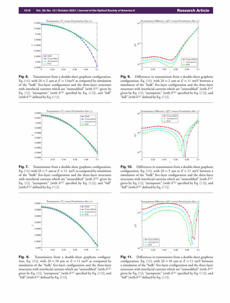
We began with low-energy illumination at E = 11 meV(corresponding to λ≈ 112.7129 µm) and display results ofthe transmission in Figs. 6 (2h = 2 µm), 7 (2h = 5 µm), and8 (2h = 10 µm) as computed by simulation of the “bulk”five-layer problem, and the three-layer configurations withconductivities specified by the “no modification,” “asymp-totic,” and “full” models specified above. In addition, in Figs. 9(2h = 2 µm), 10 (2h = 5 µm), and 11 (2h = 10 µm), weshow the differences between these latter three and the bulksimulation which we consider exact.
Remark 4.3. Once again, all three models do give goodresults, but the “full” model gives the best results for most valuesof ε sampled (0≤ ε≤ 0.075, at least) being exact to machineprecision when ε= 0.
We concluded with high-energy illumination atE = 26 meV (corresponding to λ≈ 47.6862 µm) anddisplay results of the transmission in Figs. 12 (2h = 2 µm),13 (2h = 5 µm), and 14 (2h = 10 µm) as computed by sim-ulation of the “bulk” five-layer problem, and the three-layer
1518 Vol. 38, No. 10 / October 2021 / Journal of the Optical Society of America A Research Article
0 0.02 0.04 0.06 0.08 0.10.4048
0.405
0.4052
0.4054
0.4056
0.4058
0.406
0.4062
0.4064
Fig. 6. Transmission from a double-sheet graphene configuration,Eq. (16), with 2h = 2 µm at E = 11meV as computed by simulationof the “bulk” five-layer configuration and the three-layer structureswith interfacial currents which are “unmodified” [with σ (g ) given byEq. (1)], “asymptotic” [with σ (g ) specified by Eq. (12)], and “full”[with σ (g ) defined by Eq. (11)].
0 0.02 0.04 0.06 0.08 0.10.3383
0.3384
0.3385
0.3386
0.3387
0.3388
0.3389
0.339
0.3391
0.3392
Fig. 7. Transmission from a double-sheet graphene configuration,Eq. (16), with 2h = 5 µm at E = 11 meV as computed by simulationof the “bulk” five-layer configuration and the three-layer structureswith interfacial currents which are “unmodified” [with σ (g ) given byEq. (1)], “asymptotic” [with σ (g ) specified by Eq. (12)], and “full”[with σ (g ) defined by Eq. (11)].
0 0.02 0.04 0.06 0.08 0.10.268
0.2681
0.2682
0.2683
0.2684
0.2685
0.2686
0.2687
Fig. 8. Transmission from a double-sheet graphene configura-tion, Eq. (16), with 2h = 10 µm at E = 11 meV as computed bysimulation of the “bulk” five-layer configuration and the three-layerstructures with interfacial currents which are “unmodified” [with σ (g )
given by Eq. (1)], “asymptotic” [with σ (g ) specified by Eq. (12)], and“full” [with σ (g ) defined by Eq. (11)].
0 0.02 0.04 0.06 0.08 0.1
10-5
10-4
10-3
Fig. 9. Differences in transmission from a double-sheet grapheneconfiguration, Eq. (16), with 2h = 2 µm at E = 11 meV between asimulation of the “bulk” five-layer configuration and the three-layerstructures with interfacial currents which are “unmodified” [with σ (g )
given by Eq. (1)], “asymptotic” [with σ (g ) specified by Eq. (12)], and“full” [with σ (g ) defined by Eq. (11)].
0 0.02 0.04 0.06 0.08 0.1
10-6
10-5
10-4
Fig. 10. Differences in transmission from a double-sheet grapheneconfiguration, Eq. (16), with 2h = 5 µm at E = 11 meV between asimulation of the “bulk” five-layer configuration and the three-layerstructures with interfacial currents which are “unmodified” [with σ (g )
given by Eq. (1)], “asymptotic” [with σ (g ) specified by Eq. (12)], and“full” [with σ (g ) defined by Eq. (11)].
0 0.02 0.04 0.06 0.08 0.110-6
10-5
Fig. 11. Differences in transmission from a double-sheet grapheneconfiguration, Eq. (16), with 2h = 10 µm at E = 11 meV betweena simulation of the “bulk” five-layer configuration and the three-layerstructures with interfacial currents which are “unmodified” [with σ (g )
given by Eq. (1)], “asymptotic” [with σ (g ) specified by Eq. (12)], and“full” [with σ (g ) defined by Eq. (11)].

Research Article Vol. 38, No. 10 / October 2021 / Journal of the Optical Society of America A 1519
0 0.02 0.04 0.06 0.08 0.10.56
0.561
0.562
0.563
0.564
0.565
0.566
Fig. 12. Transmission from a double-sheet graphene configuration,Eq. (16), with 2h = 2 µm at E = 26 meV as computed by simulationof the “bulk” five-layer configuration and the three-layer structureswith interfacial currents which are “unmodified” [with σ (g ) given byEq. (1)], “asymptotic” [with σ (g ) specified by Eq. (12)], and “full”[with σ (g ) defined by Eq. (11)].
0 0.02 0.04 0.06 0.08 0.10.488
0.489
0.49
0.491
0.492
0.493
0.494
0.495
Fig. 13. Transmission from a double-sheet graphene configuration,Eq. (16), with 2h = 5 µm at E = 26 meV as computed by simulationof the “bulk” five-layer configuration and the three-layer structureswith interfacial currents which are “unmodified” [with σ (g ) given byEq. (1)], “asymptotic” [with σ (g ) specified by Eq. (12)], and “full”[with σ (g ) defined by Eq. (11)].
0 0.02 0.04 0.06 0.08 0.10.509
0.51
0.511
0.512
0.513
0.514
0.515
0.516
0.517
Fig. 14. Transmission from a double-sheet graphene configura-tion, Eq. (16), with 2h = 10 µm at E = 26 meV as computed bysimulation of the “bulk” five-layer configuration and the three-layerstructures with interfacial currents which are “unmodified” [with σ (g )
given by Eq. (1)], “asymptotic” [with σ (g ) specified by Eq. (12)], and“full” [with σ (g ) defined by Eq. (11)].
0 0.02 0.04 0.06 0.08 0.110-5
10-4
10-3
10-2
Fig. 15. Differences in transmission from a double-sheet grapheneconfiguration, Eq. (16), with 2h = 2 µm at E = 26 meV between asimulation of the “bulk” five-layer configuration and the three-layerstructures with interfacial currents which are “unmodified” [with σ (g )
given by Eq. (1)], “asymptotic” [with σ (g ) specified by Eq. (12)], and“full” [with σ (g ) defined by Eq. (11)].
0 0.02 0.04 0.06 0.08 0.110-5
10-4
10-3
10-2
Fig. 16. Differences in transmission from a double-sheet grapheneconfiguration, Eq. (16), with 2h = 5 µm at E = 26 meV between asimulation of the “bulk” five-layer configuration and the three-layerstructures with interfacial currents which are “unmodified” [with σ (g )
given by Eq. (1)], “asymptotic” [with σ (g ) specified by Eq. (12)], and“full” [with σ (g ) defined by Eq. (11)].
configurations with conductivities specified by the “no modi-fication,” “asymptotic,” and “full” models specified previously.In addition, in Figs. 15 (2h = 2 µm), 16 (2h = 5 µm), and17 (2h = 10 µm), we show the differences between these latterthree and the bulk simulation, which we consider exact.
Remark 4.4. Again, all three models do give passable answers,but the “full” model gives the best results for all values of ε sam-pled, again being exact to machine precision when ε= 0.
E. Summary
There are crucial conclusions to draw from these results. InFigs. 3 and 5, we see that the “full” model is most accurate, andthe “asymptotic” model second, on the ranges 0≤ ε≤ 0.025and 0≤ ε≤ 0.04, respectively. Interestingly, Figs. 9, 10, and11 reveal the same relative performance of the models on themuch larger range 0≤ ε≤ 0.075. Finally, from Figs. 15–17,we learn that the same ordering holds over the entire range of εthat we studied. From this, we conclude that the “full” model we

1520 Vol. 38, No. 10 / October 2021 / Journal of the Optical Society of America A Research Article
0 0.02 0.04 0.06 0.08 0.110-6
10-5
10-4
10-3
10-2
Fig. 17. Differences in transmission from a double-sheet grapheneconfiguration, Eq. (16), with 2h = 10 µm at E = 26 meV betweena simulation of the “bulk” five-layer configuration and the three-layerstructures with interfacial currents which are “unmodified” [with σ (g )
given by Eq. (1)], “asymptotic” [with σ (g ) specified by Eq. (12)], and“full” [with σ (g ) defined by Eq. (11)].
describe is always more accurate for ε sufficiently small, and insome cases the range of ε can be quite large.
Funding. National Science Foundation (DMS-1813033);Simons Foundation; National Research Foundation of Korea(NRF-2021R1A2C1093579).
Acknowledgment. D. P. N. gratefully acknowledges support fromthe NSF. Y. H. gratefully acknowledges support from a CollaborationGrant for Mathematicians, Simons Foundation, and National ResearchFoundation of Korea (NRF) funded by the Ministry of Education(NRF-2021R1A2C1093579),
Disclosures. The authors declare no conflicts of interest.
Data Availability. Data underlying the results presented in this paper arenot publicly available at this time but may be obtained from the authors uponreasonable request.
REFERENCES1. F. Bonaccorso, Z. Sun, T. Hasan, and A. C. Ferrari, “Graphene pho-
tonics and optoelectronics,” Nat. Photonics 4, 611–622 (2010).2. A. Geim, “Random walk to graphene (Nobel lecture),” Angew. Chem.
(Int. Ed.) 50, 6966–6985 (2011).3. K. Novoselov, “Graphene: materials in the flatland (Nobel lecture),”
Angew. Chem. (Int. Ed.) 50, 6986–7002 (2011).4. A. N. Grigorenko, M. Polini, and K. S. Novoselov, “Graphene
plasmonics,” Nat. Photonics 6, 749–758 (2012).5. T. Low, A. Chaves, J. Caldwell, A. Kumar, N. Fang, P. Avouris, T.
Heinz, F. Guinea, L. Martin-Moreno, and F. Koppens, “Polaritons inlayered two-dimensional materials,” Nat. Mater. 16, 182–194 (2017).
6. D. N. Basov, M. M. Fogler, and F. J. Garca de Abajo, “Polaritons inVan der Waals materials,” Science 354, aag1992 (2016).
7. D. Alcaraz Iranzo, S. Nanot, E. J. C. Dias, I. Epstein, C. Peng, D.K. Efetov, M. B. Lundeberg, R. Parret, J. Osmond, J.-Y. Hong, J.Kong, D. R. Englund, N. M. R. Peres, and F. H. L. Koppens, “Probingthe ultimate plasmon confinement limits with a Van der Waalsheterostructure,” Science 360, 291–295 (2018).
8. I.-H. Lee, D. Yoo, P. Avouris, T. Low, and S.-H. Oh, “Graphene acous-tic plasmon resonator for ultrasensitive infrared spectroscopy,” Nat.Nanotechnol. 14, 313–319 (2019).
9. M. Jablan, H. Buljan, and M. Soljacic, “Plasmonics in graphene atinfrared frequencies,” Phys. Rev. B 80, 245435 (2009).
10. F. H. L. Koppens, D. E. Chang, and F. J. Garcia de Abajo, “Grapheneplasmonics: a platform for strong light-matter interactions,” NanoLett. 11, 3370–3377 (2011).
11. A. Auditore, C. de Angelis, A. Locatelli, and A. B. Aceves, “Tuning ofsurface plasmon polaritons beat length in graphene directional cou-plers,” Opt. Lett. 38, 4228–4231 (2013).
12. F. J. Garcia de Abajo, “Graphene plasmonics: challenges and oppor-tunities,” ACS Photon. 1, 135–152 (2014).
13. T. Low and P. Avouris, “Graphene plasmonics for terahertz tomid-infrared applications,” ACS Nano 8, 1086 (2014).
14. COMSOL, COMSOL Multiphysics Reference Manual (COMSOL,2019).
15. I.-H. Lee, M. He, X. Zhang, Y. Luo, S. Liu, J. H. Edgar, K. Wang, P.Avouris, T. Low, J. D. Caldwell, and S.-H. Oh, “Image polaritons inboron nitride for extreme polariton confinement with low losses,” Nat.Commun. 11, 3649 (2020).
16. B. Gallinet, J. Butet, and O. J. F. Martin, “Numerical methods fornanophotonics: standard problems and future challenges,” LaserPhoton. Rev. 9, 577–603 (2015).
17. D. P. Nicholls, “Three-dimensional acoustic scattering by lay-ered media: a novel surface formulation with operator expansionsimplementation,” Proc. R. Soc. London A 468, 731–758 (2012).
18. D. P. Nicholls, “Numerical simulation of grating structures incorporat-ing two-dimensional materials: a high-order perturbation of surfacesframework,” SIAM J. Appl. Math. 78, 19–44 (2018).
19. D. P. Nicholls, “High-order spectral simulation of graphene ribbons,”Commun. Comput. Phys. 26, 1575–1596 (2019).
20. Y. Bludov, A. Ferreira, N. Peres, and M. Vasilevskiy, “A primer onsurface plasmon-polaritons in graphene,” Int. J. Mod. Phys. B 27,1341001 (2013).
21. P. A. D. Goncalves and N. M. R. Peres, An Introduction to GraphenePlasmonics (World Scientific, 2016).
22. C. D. Angelis, A. Locatelli, A. Mutti, and A. Aceves, “Coupling dynam-ics of 1D surface plasmon polaritons in hybrid graphene systems,”Opt. Lett. 41, 480–483 (2016).
23. M. Maier, D. Margetis, and M. Luskin, “Dipole excitation of surfaceplasmon on a conducting sheet: finite element approximation andvalidation,” J. Comput. Phys. 339, 126–145 (2017).
24. M. Maier, D. Margetis, and M. Luskin, “Generation of surfaceplasmon-polaritons by edge effects,” Commun. Math. Sci. 16, 77–95(2018).
25. J. H. Song, M. Maier, and M. Luskin, “Adaptive finite element sim-ulations of waveguide configurations involving parallel 2D materialsheets,” Comput. Methods Appl. Mech. Eng. 351, 20–34 (2019).
26. D. P. Nicholls and S.-H. Oh, “Launching graphene surface plasmonwaves with vanishingly small periodic grating structures,” J. Opt.Soc. Am. A 38, 556–563 (2021).
27. R. Petit, ed., Electromagnetic Theory of Gratings (Springer-Verlag,1980).
28. Y. Hong and D. P. Nicholls, “A stable high-order perturbation of sur-faces method for numerical simulation of diffraction problems in triplylayered media,” J. Comput. Phys. 330, 1043–1068 (2017).
29. Y. Hong and D. P. Nicholls, “A high-order perturbation of surfacesmethod for scattering of linear waves by periodic multiply lay-ered gratings in two and three dimensions,” J. Comput. Phys. 345,162–188 (2017).
30. D. P. Nicholls, “Stable, high-order computation of impedance-impedance operators for three-dimensional layered mediasimulations,” Proc. R. Soc. London A 474, 20170704 (2018).
31. D. P. Nicholls, “On analyticity of scattered fields in layered structureswith interfacial graphene,” Stud. Appl. Math. 147, 527–576 (2021).
32. D. P. Nicholls and F. Reitich, “Analytic continuation of Dirichlet-Neumann operators,” Numer. Math. 94, 107–146 (2003).
33. D. P. Nicholls and M. Taber, “Joint analyticity and analytic con-tinuation for Dirichlet–Neumann operators on doubly perturbeddomains,” J. Math. Fluid Mech. 10, 238–271 (2008).
34. G. A. Baker, Jr. and P. Graves-Morris, Padé Approximants, 2nd ed.(Cambridge University, 1996).
35. B. Després, “Méthodes de décomposition de domaine pour les prob-lèmes de propagation d’ondes en régime harmonique. Le théorèmede Borg pour l’équation de Hill vectorielle,” thèse (Institut National deRecherche en Informatique et en Automatique (INRIA)/Université deParis IX, 1991).
36. B. Després, “Domain decomposition method and the Helmholtzproblem,”Mathematical andNumerical Aspects ofWave PropagationPhenomena, Strasbourg, France, SIAM, 1991, pp. 44–52.