on the observation of dispersion in tunable second-order
TRANSCRIPT
APL Photonics ARTICLE scitation.org/journal/app
On the observation of dispersion in tunablesecond-order nonlinearities of silicon-richnitride thin films
Cite as: APL Photon. 4, 036101 (2019); doi: 10.1063/1.5053704Submitted: 24 August 2018 • Accepted: 11 February 2019 •Published Online: 5 March 2019
Hung-Hsi Lin,1,a) Rajat Sharma,2,a),b) Alex Friedman,2 Benjamin M. Cromey,3 Felipe Vallini,2 Matthew W. Puckett,2Khanh Kieu,3 and Yeshaiahu Fainman2
AFFILIATIONS1Materials Science and Engineering, University of California, 9500 Gilman Drive, La Jolla, San Diego, California 92093, USA2Department of Electrical and Computer Engineering, University of California, 9500 Gilman Drive, La Jolla, San Diego,California 92093, USA
3College of Optical Sciences, The University of Arizona, 1630 E University Blvd., Tucson, Arizona 85719, USA
a)Contributions: H.-H. Lin and R. Sharma contributed equally to this work.b)Author to whom correspondence should be addressed: [email protected]
ABSTRACTWe present experimental results on second-harmonic generation in non-stoichiometric, silicon-rich nitride films. The as-deposited film presents a second-order nonlinear coefficient, or χ(2), as high as 8 pm/V. This value can be widely tuned usingthe electric field induced second harmonic effect, and a maximum value of 22.7 pm/V was achieved with this technique. We fur-ther illustrate that the second-order nonlinear coefficient exhibited by these films can be highly dispersive in nature and requirefurther study and analysis to evaluate their viability for in-waveguide applications at telecommunication wavelengths.
© 2019 Author(s). All article content, except where otherwise noted, is licensed under a Creative Commons Attribution (CC BY) license(http://creativecommons.org/licenses/by/4.0/). https://doi.org/10.1063/1.5053704
INTRODUCTION
There is an acute need for a highly nonlinear mate-rial that can be integrated with silicon to achieve effi-cient, high-speed, linear electro-optic modulation, and non-linear wave mixing.1–3 In recent years, silicon nitride hasemerged as one such promising candidate with salient fea-tures such as a wide transparency window, ease of fabri-cation and compatibility with silicon photonics manufactur-ing.4 While traditionally silicon nitride has been seen as acentrosymmetric dielectric, lacking any second-order non-linear susceptibility,5 recent results in the literature haveshown that silicon nitride can exhibit an anomalous second-order nonlinear susceptibility,6,7 the origin of which remainsunclear.
While reported results have shown the second-ordernonlinear properties of silicon nitride thin-films to vary across
deposition techniques and associated conditions, work inthe literature has not focused on the variety of wavelengthsemployed in these experimental studies. There have beenreports in the literature on thin-films of stoichiometric sil-icon nitride which have demonstrated a bulk second-ordernonlinear susceptibility, χ(2), as high as ∼3 pm/V, at a pumpwavelength of 800 nm;6,7 while other results have utilizedin-waveguide, phase-matched, second harmonic generation(SHG) to report values as low as ∼0.3 pm/V in stoichiomet-ric films at a pump wavelength of 1550 nm.7,8 Previously, theauthors have attributed this discrepancy, in measured coef-ficients using free-space and in-waveguide measurements,to a lack of perfect phase-matching and/or modificationsintroduced into the materials during fabrication.7 To the bestof our knowledge, there has not been a conclusive discus-sion or reported results thus far on this discrepancy, and itsdispersive nature, in the literature.
APL Photon. 4, 036101 (2019); doi: 10.1063/1.5053704 4, 036101-1
© Author(s) 2019
APL Photonics ARTICLE scitation.org/journal/app
In this manuscript, we undertake a systematic evaluationof the second-order nonlinear properties exhibited by sili-con nitride thin films. We discuss methods to enhance theobserved χ(2) by both increasing the silicon content in the filmsas well as through the electric-field induced second-harmoniceffect (EFISH). Finally, we also report on our observation ofa high degree of dispersion in the χ(2) exhibited by thesefilms.
SILICON-RICH NITRIDE
Bulk nonlinearities in silicon nitride thin films depositedthrough plasma enhanced chemical vapor deposition, PECVD,and RF magnetron sputtering have been reported on in thepast.6 The first measurement of this nonlinearity using in-waveguide experiments was reported in 2016,7 where theauthors carried out phase-matched second-harmonic gener-ation in stoichiometric silicon nitride waveguides. The magni-tude of the reported nonlinearity was low with in-waveguidemeasurements (at 1550 nm) yielding values of χ(2) lower than1 pm/V. These values have subsequently been reproduced andconfirmed in a separate measurement by Billat et al.8 By lever-aging a unique attribute of the silicon nitride platform, thisrelatively small nonlinearity can be enhanced by changing thestoichiometry of the deposited films. It is known that increas-ing the silicon content in sputtered silicon nitride thin films,yielding the so-called silicon-rich nitride (SRN) films, leads toan enhancement in the magnitude of the third-order non-linearity.9 However, these films suffer from high propagationloss, making them inapplicable to many in-waveguide appli-cations. There have been two recent reports10,11 extendingthese results to PECVD deposited SRN films carried out usingfree-space measurements with pump wavelengths of 800 nmand 1040 nm, respectively. The SRN material was shown topossess an enhanced second-order nonlinearity compared tothat of stoichiometric films, while its propagation loss valuesremained relatively low.
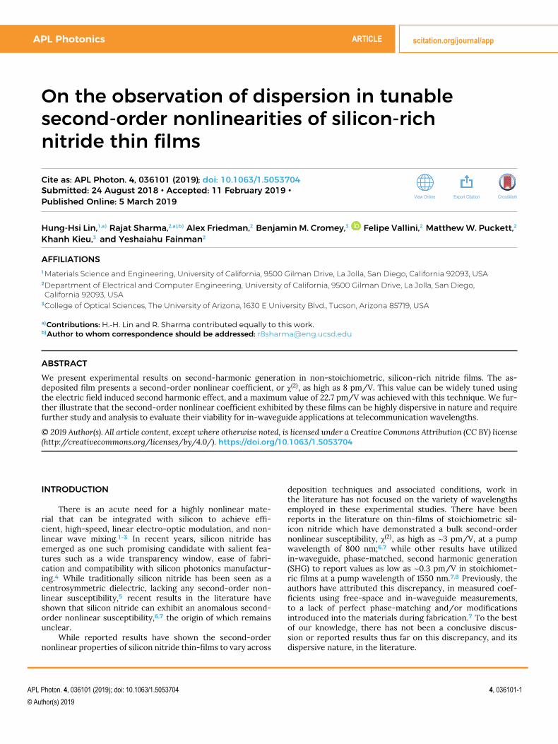
With an intent to evaluate these films for in-waveguideapplications, we carried out a systematic study of the effectof silicon content on the exhibited linear and nonlinear opti-cal properties of the films. Three different samples, labeled S1,S2, and S3, were fabricated with silicon nitride films depositedon fused-silica substrates. The flow-rate of silane (SiH4), oneof the precursors in the PECVD process, was varied acrossthe samples from 180, 276, and 500sccm, while keeping allthe other deposition parameters (outlined in Ref. 7) constant.Ellipsometry measurements using light at 632.8 nm confirmedthat this fabrication process produced films with unequalrefractive indices of 1.9 (S1), 2.08 (S2), and 2.25 (S3), with theindex of the film scaling positively with the SiH4 flow-rate.The reason for this was confirmed to be an increase in sili-con content by carrying out electron-dispersive X-ray (EDX)spectroscopic measurements. Figure 1(a) shows the composi-tion of the films in terms of their silicon and nitride atomicpercentages (shown in red and blue arrows, respectively), witha silicon content of 41% (S1), 51% (S2), and 56% (S3) across thethree films.
FREE-SPACE MEASUREMENTS
In order to characterize the effect of the silicon content inthese films on their nonlinear properties, polarization depen-dent SHG experiments were carried out using a femtosecondTi:Sapphire laser source at a wavelength of 800 nm, with apulse duration of 150 fs, an 80 MHz repetition rate, and a100 mW of average power. The pump beam was focused usinga 20×microscope objective to a focal spot on the surface of theSRN sample, with a beam waist of 50 µm and a confocal param-eter much longer than the thickness of the film. The generateds- and p-polarized SHG signals were detected as a function ofthe polarization angle of the pump. Further details of the char-acterization setup can be found in the supplementary material.All of the SiN thin films were grown to the same thickness of400 nm and were deposited on 1.5 cm × 1.5 cm fused silica
FIG. 1. (a) Composition of the samples, S1, S2, and S3, in terms of the atomic percentages of silicon and nitrogen, extracted using EDX spectroscopy. (b) Second-harmonicsignals generated from the three films as a function of polarization angle for p-polarization. (c) SHG signals from the SRN film (S3) for both s- and p-polarized input pumps.
APL Photon. 4, 036101 (2019); doi: 10.1063/1.5053704 4, 036101-2
© Author(s) 2019
APL Photonics ARTICLE scitation.org/journal/app
TABLE I. The deposition recipes and measured properties of silicon nitride thin films.
SiH4 flow Refractive index χ(2)zzz χ(2)
zxxSample rate (sccm) Si (%) (λ = 632.8 nm) (pm/V) (pm/V)
S1 180 41 1.9 2.4 0.4S2 276 51 2.08 5.8 1.1S3 500 56 2.25 8 1.9
substrates. A commercial 500 µm thick X-cut quartz wafer,exhibiting a nonlinear coefficient χ(2)
xxx of 0.64% ± 8% pm/Vis used to calibrate the system, and the absolute values ofχ(2) tensor components from our samples are determined bycomparing the generated SHG signals with those from thequartz sample under the same experimental conditions. Theuse of thin-films in this study helps to avoid the need for anyphase-matching, including the need to account for dispersionin the linear refractive index in the silicon nitride films, whilecalculating the generated second-harmonic power using therevised Maker-fringes analysis.7 For example, in the case of a400 nm thick SRN film (n = 2.25 at λpump = 800 nm), a relativelyhigh dispersion of up to 10−2 in linear refractive index fromthe pump to the second-harmonic wavelength (λSHG = 400 nm)would cause a change of only 0.04% in the calculated second-harmonic power and hence dispersion in linear refractiveindex can be neglected. Additionally, it should be noted thatthe measurement errors in this study originate mainly fromthe fluctuation of laser power due to the unstable humidity ofenvironment (±5%), fluctuation of readings from photomulti-plier tube (PMT) resulting from the influence of backgroundnoises (±20%), and the non-uniformity in the thickness of thedeposited thin films (±10%). Besides, the possibility of countingerror (±10%) of photons in the PMT (Hamamatsu, Inc., H11461-03) due to pulse-overlapping, as described in the handbook,is also taken into account.13 Furthermore, in order to mini-mize these errors, the generated SHG intensities from quartzand SiN thin films are determined by the average of five differ-ent spots on each sample. The revised Maker fringes analysiswas then employed to carry out the tensorial analysis of thesecond-order nonlinearity.7,11–13 As is evident from the fig-ure, the generated second-harmonic signal from the film with
the highest silicon content (S3) is up to 10 times larger com-pared to that generated from the film with a stoichiometriccomposition (S1). Additionally, these polarization dependentsecond-harmonic responses were then used to extract thetensorial components of the observed χ(2) in these films. Theextracted values of the all-normal (χ(2)
zzz) and in-plane (χ(2)zxx)
components are tabulated in Table I and are found to be up to3.3 times larger for the SRN film (sample S3) when comparedwith the stoichiometric film (sample S1). Furthermore, to thebest of our knowledge, the measured tensor component χ(2)
zzzin the SRN film is the largest reported to-date in as-depositedPECVD silicon nitride films, and the experimental results alsoverify that the increasing silicon content in SiN thin films leadsto enhancement in the second order nonlinear susceptibility.
ELECTRIC FIELD INDUCED ENHANCEMENTIN NONLINEARITIES
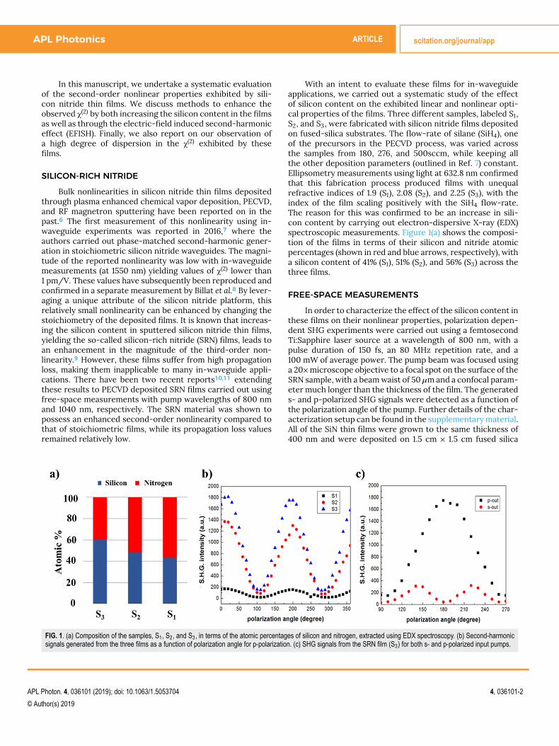
An alternative method to enhance the nonlinear responsein these films is the electric-field induced second-harmonic(EFISH) effect. In our previous work,7 we presentedin-waveguide results demonstrating enhancement of thesecond-harmonic response from silicon nitride waveguides byapplying an electric field across them. It was shown then thatthe applied external electric field interacts with the third-order nonlinearity of the films, resulting in a higher effec-tive second-order response and a corresponding increase inthe intensity of the second-harmonic signal from the waveg-uides.7 To analyze the tunability of the nonlinear response inthe SRN films, we fabricated 50 nm thick films of the three sili-con nitride films sandwiched between two electrodes made of10 nm thick layers of indium tin oxide (ITO) on a fused siliconsubstrate, as shown in the schematic in Fig. 2(a). The ITO filmsserve as the transparent electrodes across which an externalDC voltage is applied while carrying out SHG experiments. Itshould be noted that while the ITO films were not optimizedwith respect to their conductance, they were still sufficient forcarrying out preliminary studies on the EFISH induced tun-ability in the films. Figure 2(b) shows the SHG response forthe SRN film, with pump and second-harmonic wavelengthsof 800 and 400 nm, respectively, as a function of the applied
FIG. 2. (a) Schematic illustration ofthe SHG response (λpump = 800 nm,λSHG = 400 nm) from a 50 nm sili-con nitride film sandwiched between two10 nm ITO films on a fused silica sub-strate. (b) Experimental (black dots) andquadratic fitting (red) curve showing theSHG response from a SRN sample as afunction of the external voltage appliedacross the layer.
APL Photon. 4, 036101 (2019); doi: 10.1063/1.5053704 4, 036101-3
© Author(s) 2019
APL Photonics ARTICLE scitation.org/journal/app
TABLE II. As-deposited, lowest and highest effective χ(2) of three different siliconnitride films with different silicon contents. The highest range of tunability is exhibitedby the SRN film with a value of χ(2) as high as 22.7 pm/V.
χ(2)eff
SiH4 flow (no bias) Lowest χ(2)eff Highest χ(2)
effSample rate (sccm) (pm/V) (pm/V) (pm/V)
S1∗ 180 2.6 2.1 3.9
S2∗ 276 3.35 2.39 5.93
S3∗ 500 7.5 3.9 22.7
voltage, clearly demonstrating a wide range of tunability. TheSHG response is found to increase quadratically with respectto the applied voltage, which is in agreement with our pre-diction of EFISH. It should also be noted that the minimumin the measured quadratic response is found to be at a smallnegative bias voltage and not at zero-bias. This is because atthis voltage, the artificially created second-order nonlinearitygenerated by the external electric field and the high χ(3) coef-ficient of SiN perfectly negates the all-normal χ(2)
zzz presentin the as-deposited film. As a result, the magnitude of theSHG response reduces but is still not perfectly zero because ofcontributions from the in-plane components of the χ(2) in theas-deposited nitride film, ITO layers, as well as those arisingout of any surface nonlinearities.
The SHG signal measured at an applied voltage of 8 V wasfound to be up to 36 times larger than that measured at zero-bias. Table II summarizes the calculated highest and lowesteffective χ(2)
zzz components of three different silicon nitridesamples fabricated with the same silicon contents as S1, S2, andS3. The SRN film demonstrates an effective χ(2) spanning from∼3 pm/V to as high as 22 pm/V. This relatively large rangeof tunability is in accordance with reports in the literatureof an enhanced third-order nonlinear response in silicon-richnitride films when compared to their stoichiometric counter-parts14–16
DISPERSION IN THE OBSERVED NONLINEARITY
The bulk of the studies on second-order nonlinearitiesin silicon nitride films have been carried out using either
800 nm or 1064 nm sources.6,11 While the values of nonlin-earities reported using these pump wavelengths are relativelyhigh, other studies which pursue in-waveguide experimentsat a pump wavelength of 1550 nm have measured lower valuesof the nonlinearity.7,8 The cause of this discrepancy betweenvalues measured using two different pump-wavelengths wasattributed previously to a lack of perfect phase-matching inwaveguide SHG experiments carried out using a pump at1550 nm.
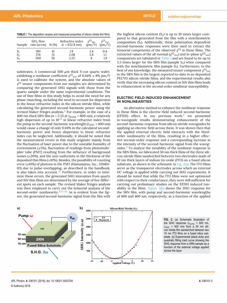
To test for wavelength dependence in the nonlinearitiesof our films, we carried out reflection SHG measurements onall three samples, using pumps at 1040 nm and 1550 nm. Thesetwo wavelengths were chosen solely based on source avail-ability. The exact methodology employed in carrying out thesemeasurements is detailed in the supplementary material, whilethe optical setup is shown in Fig. 3(a). To make a fair com-parison, parameters such as an incident angle, spot size ofthe beam, average pump power, and polarization state werekept constant while carrying out the measurements across thethree samples. Figure 3(b) shows the magnitude of the SHGsignal, corresponding to the polarization with the maximumsecond-harmonic signal, generated from the three samplesat the two pump-wavelengths. Sample S3, with the highestsilicon content, demonstrates the largest second-harmonicsignal among the three samples at both pump wavelengths.
Dispersion in nonlinear susceptibilities is a well-knownphenomenon explained by Miller’s rule, which defines a rela-tion between dispersion in refractive index and dispersion insecond-order nonlinearities.18,19 Furthermore, work in the lit-erature has shown a correlation between increasing siliconcontent in silicon nitride films and the dispersion in refrac-tive index of such films.11 These two facts together imply thatdispersion in χ(2) is expected from 1040 nm to 1550 nm andexpected to be the highest in the film with the highest siliconcontent. However, the magnitude of dispersion demonstratedin this work far exceeds that predicted by Miller’s rule andtherefore the exact origins of this remains to be explained.Specifically, a difference in magnitude of second harmonicgeneration between 1040 nm and 1550 nm of 41, 42, and 39times is seen across the three films S3, S2, and S1, respectively.Since the power in the second-harmonic signal is proportionalto the square of the second-order nonlinear coefficient, this
FIG. 3. (a) Schematic of the reflec-tion mode second-harmonic generationsetup. (b) The generated reflected p-polarized SHG signals from the threesamples, corresponding to pump wave-lengths of 1040 nm (red bars) and1550 nm (blue bars).
APL Photon. 4, 036101 (2019); doi: 10.1063/1.5053704 4, 036101-4
© Author(s) 2019
APL Photonics ARTICLE scitation.org/journal/app
implies that the effective χ(2) value measured using a 1550 nmpump is smaller by up to ∼6.4 times than that measured usinga 1040 nm pump.
IN-WAVEGUIDE LOSS CHARACTERIZATIONS
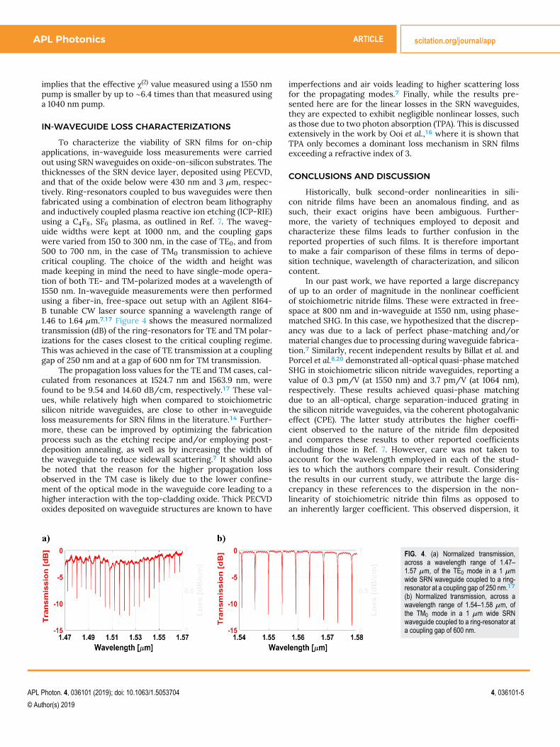
To characterize the viability of SRN films for on-chipapplications, in-waveguide loss measurements were carriedout using SRN waveguides on oxide-on-silicon substrates. Thethicknesses of the SRN device layer, deposited using PECVD,and that of the oxide below were 430 nm and 3 µm, respec-tively. Ring-resonators coupled to bus waveguides were thenfabricated using a combination of electron beam lithographyand inductively coupled plasma reactive ion etching (ICP-RIE)using a C4F8, SF6 plasma, as outlined in Ref. 7. The waveg-uide widths were kept at 1000 nm, and the coupling gapswere varied from 150 to 300 nm, in the case of TE0, and from500 to 700 nm, in the case of TM0 transmission to achievecritical coupling. The choice of the width and height wasmade keeping in mind the need to have single-mode opera-tion of both TE- and TM-polarized modes at a wavelength of1550 nm. In-waveguide measurements were then performedusing a fiber-in, free-space out setup with an Agilent 8164-B tunable CW laser source spanning a wavelength range of1.46 to 1.64 µm.7,17 Figure 4 shows the measured normalizedtransmission (dB) of the ring-resonators for TE and TM polar-izations for the cases closest to the critical coupling regime.This was achieved in the case of TE transmission at a couplinggap of 250 nm and at a gap of 600 nm for TM transmission.
The propagation loss values for the TE and TM cases, cal-culated from resonances at 1524.7 nm and 1563.9 nm, werefound to be 9.54 and 14.60 dB/cm, respectively.17 These val-ues, while relatively high when compared to stoichiometricsilicon nitride waveguides, are close to other in-waveguideloss measurements for SRN films in the literature.14 Further-more, these can be improved by optimizing the fabricationprocess such as the etching recipe and/or employing post-deposition annealing, as well as by increasing the width ofthe waveguide to reduce sidewall scattering.7 It should alsobe noted that the reason for the higher propagation lossobserved in the TM case is likely due to the lower confine-ment of the optical mode in the waveguide core leading to ahigher interaction with the top-cladding oxide. Thick PECVDoxides deposited on waveguide structures are known to have
imperfections and air voids leading to higher scattering lossfor the propagating modes.7 Finally, while the results pre-sented here are for the linear losses in the SRN waveguides,they are expected to exhibit negligible nonlinear losses, suchas those due to two photon absorption (TPA). This is discussedextensively in the work by Ooi et al.,16 where it is shown thatTPA only becomes a dominant loss mechanism in SRN filmsexceeding a refractive index of 3.
CONCLUSIONS AND DISCUSSION
Historically, bulk second-order nonlinearities in sili-con nitride films have been an anomalous finding, and assuch, their exact origins have been ambiguous. Further-more, the variety of techniques employed to deposit andcharacterize these films leads to further confusion in thereported properties of such films. It is therefore importantto make a fair comparison of these films in terms of depo-sition technique, wavelength of characterization, and siliconcontent.
In our past work, we have reported a large discrepancyof up to an order of magnitude in the nonlinear coefficientof stoichiometric nitride films. These were extracted in free-space at 800 nm and in-waveguide at 1550 nm, using phase-matched SHG. In this case, we hypothesized that the discrep-ancy was due to a lack of perfect phase-matching and/ormaterial changes due to processing during waveguide fabrica-tion.7 Similarly, recent independent results by Billat et al. andPorcel et al.8,20 demonstrated all-optical quasi-phase matchedSHG in stoichiometric silicon nitride waveguides, reporting avalue of 0.3 pm/V (at 1550 nm) and 3.7 pm/V (at 1064 nm),respectively. These results achieved quasi-phase matchingdue to an all-optical, charge separation-induced grating inthe silicon nitride waveguides, via the coherent photogalvaniceffect (CPE). The latter study attributes the higher coeffi-cient observed to the nature of the nitride film depositedand compares these results to other reported coefficientsincluding those in Ref. 7. However, care was not taken toaccount for the wavelength employed in each of the stud-ies to which the authors compare their result. Consideringthe results in our current study, we attribute the large dis-crepancy in these references to the dispersion in the non-linearity of stoichiometric nitride thin films as opposed toan inherently larger coefficient. This observed dispersion, it
FIG. 4. (a) Normalized transmission,across a wavelength range of 1.47–1.57 µm, of the TE0 mode in a 1 µmwide SRN waveguide coupled to a ring-resonator at a coupling gap of 250 nm.17
(b) Normalized transmission, across awavelength range of 1.54–1.58 µm, ofthe TM0 mode in a 1 µm wide SRNwaveguide coupled to a ring-resonator ata coupling gap of 600 nm.
APL Photon. 4, 036101 (2019); doi: 10.1063/1.5053704 4, 036101-5
© Author(s) 2019
APL Photonics ARTICLE scitation.org/journal/app
should be noted, is much higher than what can be attributedto Miller’s rule,18 which relates the relative magnitude of thenonlinear susceptibilities to the linear susceptibilities at therespective wavelengths. The exact origin of this high disper-sion remains to be explained. Finally, this study’s use of thin-films was carefully chosen to be performed in free space toavoid the need for phase matching of any kind, neither all opti-cal quasi-phase matching nor modal dispersion-based phasematching.
In summary, this work has clearly demonstrated thatincreasing silicon content in PECVD deposited silicon nitridefilms results in enhancement in the second-order nonlinear-ity of such films, achieving a value as high as 8 pm/V in as-deposited SRN films. We then demonstrate a relatively largetunability range of the nonlinear coefficient, with a high-est demonstrable coefficient of 22 pm/V. Furthermore, wedemonstrate that the inherent nonlinearity in as-depositedfilms is highly dispersive, not just in the case of silicon-richcompositions but also in the case of stoichiometric films.Finally, it is our opinion that the highly dispersive nature of thesecond-order nonlinearity in these films should be taken intoconsideration by any future studies comparing the nonlinear-ity and/or evaluating the viability of such films for on-chipnonlinear and or electro-optic applications.
SUPPLEMENTARY MATERIAL
A brief description of the optical characterization setupsemployed to carry out both the maker fringes analysis and thedispersion studies of the second order nonlinear susceptibilityare included in the supplementary material.
ACKNOWLEDGMENTSThis work was supported by the Defense Advanced
Research Projects Agency (DARPA), the National ScienceFoundation (NSF), the NSF ERC CIAN, NSF’s NNCI San DiegoNanotechnology Infrastructure (SDNI), the NSF GraduateResearch Fellowship under No. DGE-1143953, the Office ofNaval Research (ONR) Multidisciplinary University ResearchInitiative (MURI), the Army Research Office (ARO), and theCymer Corporation. We thank UCSD’s staff Ryan Anderson forthe discussion on the equipment for electrical characteriza-tion.
REFERENCES1C. Malgrange, C. Ricolleau, and M. Schlenker, Symmetry and PhysicalProperties of Crystals (Springer, 2014).2R. S. Jacobsen, K. N. Andersen, P. I. Borel, J. Fage-Pedersen, L. H.Frandsen, O. Hansen, A. V. Martin Kristensen Lavrinenko, G. Moulin, H. Ou,and C. Peucheret, Nature 441(7090), 199 (2006).3M. Cazzanelli, F. Bianco, E. Borga, G. Pucker, M. Ghulinyan, E. Degoli,E. Luppi, V. Véniard, S. Ossicini, D. Modotto, and S. Wabnitz, Nat. Mater.11(2), 148 (2012).4D. J. Moss, R. Morandotti, A. L. Gaeta, and M. Lipson, Nat. Photonics 7(8),597 (2013).5J. S. Levy, M. A. Foster, A. L. Gaeta, and M. Lipson, Opt. Express 19(12), 11415–11421 (2011).6T. Ning, H. Pietarinen, O. Hyvarinen, J. Simonen, G. Genty, and M.Kauranen, Appl. Phys. Lett. 100, 161902 (2012).7M. W. Puckett, R. Sharma, H. Lin, M. Yang, F. Vallini, and Y. Fainman, Opt.Express 24, 16923 (2016).8A. Billat, D. Grassani, M. HP Pfeiffer, S. Kharitonov, T. J. Kippenberg, andB. Camille-Sophie, Nat. Commun. 8(1), 1016 (2017).9A. Kitao, K. Imakita, I. Kawamura, and M. Fujii, J. Phys. D: Appl. Phys. 47,215101 (2014).10H. Lin, R. Sharma, M. Yang, M. W. Puckett, C. D. Wurm, F. Vallini, andY. Fainman, in CLEO: Science and Innovations (Optical Society of America,2017), pp. SM1M-6.11K. Koskinen, R. Czaplicki, A. Slablab, T. Ning, A. Hermans, B. Kuyken,V. Mittal, G. S. Murugan, T. Niemi, R. Baets, and M. Kauranen, Opt. Lett.42(23), 5030–5033 (2017).12H. Lin, M. Yang, R. Sharma, M. W. Puckett, S. Montoya, C. D. Wurm,F. Vallini, E. E. Fullerton, and Y. Fainman, Appl. Phys. Lett. 110, 113103(2017).13H. Lin, F. Vallini, M. Yang, R. Sharma, M. W. Puckett, S. Montoya,C. D. Wurm, E. E. Fullerton, and Y. Fainman, Sci. Rep. 7, 9983 (2017).14J. W. Choi, G. F. R. Chen, D. K. T. Ng, K. J. A. Ooi, and D. T. H. Tan, Sci. Rep.6, 27120 (2016).15C. Lacava, S. Stankovic, A. Z. Khokhar, T. D. Bucio, F. Y. Gardes, G. T. Reed,D. J. Richardson, and P. Petropoulos, Sci. Rep. 7(1), 22 (2017).16K. J. A. Ooi, D. K. T. Ng, T. Wang, A. K. L. Chee, S. K. Ng, Q. Wang, L. K. Ang,A. M. Agarwal, L. C. Kimerling, and D. T. H. Tan, Nat. Commun. 8, 13878(2017).17R. Sharma, M. W. Puckett, H. Lin, A. Isichenko, F. Vallini, and Y. Fainman,Opt. Lett. 41(6), 1185–1188 (2016).18R. C. Miller, Appl. Phys. Lett. 5(1), 17–19 (1964).19A. Hermans, C. Kieninger, K. Koskinen, A. Wickberg, E. Solano, J.Dendooven, M. Kauranen, S. Clemmen, M. Wegener, C. Koos, and R. Baets,Sci. Rep. 7, 44581 (2017).20M. A. G. Porcel, J. Mak, C. Taballione, V. K. Schermerhorn, J. P. Epping,P. J. M. V. D. Slot, and K. J. Boller, Opt. Express 25(26), 33143–33159(2017).
APL Photon. 4, 036101 (2019); doi: 10.1063/1.5053704 4, 036101-6
© Author(s) 2019