on the sizing of analog integrated circuits towards ... · on the sizing of analog integrated...
TRANSCRIPT
TECHNISCHE UNIVERSITÄT MÜNCHEN
Lehrstuhl für Entwurfsautomatisierung
On the Sizing of Analog Integrated Circuits towardsLifetime Robustness
Xin Pan
Vollständiger Abdruck der von der Fakultät für Elektrotechnik und Informations-technik der Technischen Universität München zur Erlangung des akademischenGrades eines
Doktor-Ingenieurs
genehmigten Dissertation.
Vorsitzender: Univ.-Prof. Dr. sc. techn. Andreas Herkersdorf
Prüfer der Dissertation: 1. Priv.-Doz. Dr.-Ing. Helmut Gräb
2. Univ.-Prof. Dr. rer. nat. Doris Schmitt-Landsiedel
Die Dissertation wurde am 31.10.2012 bei der Technischen Universität Müncheneingereicht und durch die Fakultät für Elektrotechnik und Informationstechnik am22.05.2013 angenommen.

A paperback version of this thesis was published by Verlag Dr. Hut, Munich, in 2013.
ISBN 978-3-8439-1198-6.

Acknowledgements
From March 2008 to October 2012, I worked as a research assistant at the analogCAD group of Institute for Electronic Design Automation, Technische UniversitaetMuenchen. During this period , I had the opportunity to work with many nice peo-ple, colleagues and friends, with wonderful ideas and personalities. I would like toexpress my deep gratitude to them, without whom my doctoral research would notbe successful.
Firstly I would like to thank Professor Ulf Schlichtmann for giving me the chance towork at the institute, as well as for his warm help during my Master study at the uni-versity. Thanks to the Master program, I had the opportunity to come to Germanyand studied my favorite subjects, with contacts to many nice colleagues around sev-eral institutes already during that period.
My special thanks go to my doctoral research supervisor, PD Dr.-Ing. Helmut Graeb.He opened the gate of analog CAD to me with interesting topics and emerging phys-ical effects of semiconductor technologies. I remember every moment we discussedideas, checked formulas, shared progress and chatted for fun. He always motivatedme to proceed in my research with warm encouragement and constructive feedbackswhich I appreciate very much. I thank him also for the time and efforts in proofread-ing all my publications, thesis and presentation slides.
I would like to thank all of the colleagues at the institute, especially the membersof the analog group, namely Dr. Daniel Mueller, Dr. Tobias Massier, Husni Habal,Michael Eick, Michael Pehl, Michael Zwerger and Aurélien Tchegho. The fruitfuldiscussions during the study and research, valuable feedbacks on presentations andresults, as well as the colorful events organized by them will be the most cherishedpiece of memories in my life.
Last but not least, I would like to express my deep gratitude to my parents Gang andBaozhen for their continuous and invaluable encouragement. Sincerely, I thank mywife Chang for her very kind understanding and solid supports all the time, and mylovely baby Keyun for bringing us the endless happiness.
Many thanks to you all.
Munich, October 2012
Xin Pan


Contents
1 Introduction 11.1 Motivation . . . . . . . . . . . . . . . . . . . . . . . . . . . . . . . . . . . 11.2 Analog Design . . . . . . . . . . . . . . . . . . . . . . . . . . . . . . . . . 3
1.2.1 Typical Flow of Analog Integrated Circuit Design . . . . . . . . 31.2.2 Discussions and Challenges . . . . . . . . . . . . . . . . . . . . . 5
1.3 Contributions of this Thesis . . . . . . . . . . . . . . . . . . . . . . . . . 61.3.1 Study on Joint Effects of Process Variations and Transistor Aging 61.3.2 Design Flow for Lifetime Robustness Optimization . . . . . . . 71.3.3 Analytical Modeling for Aged Yield Prediction . . . . . . . . . . 7
1.4 Previous Publications . . . . . . . . . . . . . . . . . . . . . . . . . . . . . 81.5 Organization of this Thesis . . . . . . . . . . . . . . . . . . . . . . . . . . 81.6 Summary . . . . . . . . . . . . . . . . . . . . . . . . . . . . . . . . . . . . 8
2 Reliability Issues 112.1 Process Variations . . . . . . . . . . . . . . . . . . . . . . . . . . . . . . . 112.2 Reliability . . . . . . . . . . . . . . . . . . . . . . . . . . . . . . . . . . . 12
2.2.1 Reliability Function R(t) and Failure Rate z(t) . . . . . . . . . . 122.2.2 Negative Bias Temperature Instability . . . . . . . . . . . . . . . 152.2.3 Hot Carrier Injection . . . . . . . . . . . . . . . . . . . . . . . . . 182.2.4 Time-Dependent Dielectric Breakdown . . . . . . . . . . . . . . 192.2.5 Electromigration . . . . . . . . . . . . . . . . . . . . . . . . . . . 19
2.3 State of the Art . . . . . . . . . . . . . . . . . . . . . . . . . . . . . . . . . 202.3.1 Reliability Simulation . . . . . . . . . . . . . . . . . . . . . . . . 202.3.2 Solutions towards Transistor Aging . . . . . . . . . . . . . . . . 212.3.3 Design Centering considering Process Variations . . . . . . . . . 23
2.3.3.1 Statistical Methods . . . . . . . . . . . . . . . . . . . . 232.3.3.2 Deterministic Methods . . . . . . . . . . . . . . . . . . 25
2.3.4 Joint Effects of Transistor Aging and Process Variations . . . . . 272.4 Summary . . . . . . . . . . . . . . . . . . . . . . . . . . . . . . . . . . . . 29
3 Problem Formulation 313.1 Age and Lifetime . . . . . . . . . . . . . . . . . . . . . . . . . . . . . . . 31
I

3.2 Parameters . . . . . . . . . . . . . . . . . . . . . . . . . . . . . . . . . . . 323.2.1 Design Parameters . . . . . . . . . . . . . . . . . . . . . . . . . . 323.2.2 Statistical Parameters with Aging . . . . . . . . . . . . . . . . . 333.2.3 Operating Parameters . . . . . . . . . . . . . . . . . . . . . . . . 35
3.3 Performances with Aging . . . . . . . . . . . . . . . . . . . . . . . . . . 363.4 Fresh Yield and Aged Yield . . . . . . . . . . . . . . . . . . . . . . . . . 37
3.4.1 Definition . . . . . . . . . . . . . . . . . . . . . . . . . . . . . . . 373.4.2 Statistical Analysis Method . . . . . . . . . . . . . . . . . . . . . 40
3.5 Sizing Rules with Aging . . . . . . . . . . . . . . . . . . . . . . . . . . . 433.6 Summary . . . . . . . . . . . . . . . . . . . . . . . . . . . . . . . . . . . . 45
4 Aged Yield Optimization with Fresh and Aged Sizing Rules 474.1 Worst-Case Distance . . . . . . . . . . . . . . . . . . . . . . . . . . . . . 47
4.1.1 Yield Analysis and Worst-Case Analysis . . . . . . . . . . . . . . 474.1.2 Yield Estimation Based on Worst-Case Distance . . . . . . . . . 504.1.3 Problem Formulation towards Worst-Case Distance Based
Yield Estimation . . . . . . . . . . . . . . . . . . . . . . . . . . . 544.1.4 Solution using Lagrangian Functions . . . . . . . . . . . . . . . 56
4.2 Aged Worse-Case Distance and Aged Yield . . . . . . . . . . . . . . . . 594.3 Design Flow . . . . . . . . . . . . . . . . . . . . . . . . . . . . . . . . . . 61
4.3.1 Simulation Flow of the Aged Circuit . . . . . . . . . . . . . . . . 614.3.2 Fresh and Aged Sizing Rules of a Circuit . . . . . . . . . . . . . 654.3.3 Circuit Layout Area Estimation . . . . . . . . . . . . . . . . . . . 654.3.4 Optimization of Fresh Circuit with Fresh and Aged Sizing
Rules Checking and Maximum Area Constraints . . . . . . . . . 664.3.5 Aged Yield Analysis . . . . . . . . . . . . . . . . . . . . . . . . . 70
4.4 Summary . . . . . . . . . . . . . . . . . . . . . . . . . . . . . . . . . . . . 71
5 Aged Yield Prediction 735.1 Aged Worst-Case Distance Prediction Model . . . . . . . . . . . . . . . 75
5.1.1 Idea . . . . . . . . . . . . . . . . . . . . . . . . . . . . . . . . . . . 755.1.2 Linear Performance Model at t1 . . . . . . . . . . . . . . . . . . . 755.1.3 Mapping from t0 to t1 . . . . . . . . . . . . . . . . . . . . . . . . 775.1.4 Prediction of βw,U(t1) . . . . . . . . . . . . . . . . . . . . . . . . 775.1.5 Second Order Sensitivity Term . . . . . . . . . . . . . . . . . . . 79
5.2 Algorithm for the Aged Yield Prediction . . . . . . . . . . . . . . . . . . 805.3 Summary . . . . . . . . . . . . . . . . . . . . . . . . . . . . . . . . . . . . 81
6 Experimental Results 836.1 Miller Operational Amplifier . . . . . . . . . . . . . . . . . . . . . . . . 83

6.1.1 Circuit Topology . . . . . . . . . . . . . . . . . . . . . . . . . . . 836.1.2 Circuit Performances and their Specifications . . . . . . . . . . . 846.1.3 Results on Aged Yield Optimization . . . . . . . . . . . . . . . . 876.1.4 Results on Aged Yield Prediction . . . . . . . . . . . . . . . . . . 90
6.2 Folded Cascode Operational Amplifier . . . . . . . . . . . . . . . . . . . 926.2.1 Results on Aged Yield Optimization . . . . . . . . . . . . . . . . 926.2.2 Results on Aged Yield Prediction . . . . . . . . . . . . . . . . . . 94
6.3 Summary . . . . . . . . . . . . . . . . . . . . . . . . . . . . . . . . . . . . 96
7 Conclusion 97
Bibliography 99
Lists 111List of Figures . . . . . . . . . . . . . . . . . . . . . . . . . . . . . . . . . . . . 111List of Tables . . . . . . . . . . . . . . . . . . . . . . . . . . . . . . . . . . . . . 113
Abstract in German 115


Chapter 1
Introduction
1.1 Motivation
Entering the 2010’s, a huge progress in the electrical engineering and informationtechnology changes our daily life in various ways. For example, the traditionalcell phone has been gradually replaced by the smartphones and multi-function cellphones [wikb], which are capable of running various applications based on their mo-bile operating platforms. They integrate together various functions such as digitalcamera and video recorder, GPS receiver, accelerometer, wireless internet connectionsand so on. The spread of the tablet personal computer (Tablet PC) [wikc] also givespeople a totally different view about how a computer can be used and played on onesingle touchscreen which serves as both input and output devices . Another exampleis in the automotive industry [eet]. A typical modern car responds to driver’s com-mands and environmental conditions in a way which is much smarter, faster andsafer than ever before. More and more functions of the car are assisted automati-cally by microcontrollers in real time, such as driving, controlling, safety functions,navigation and entertainment systems, etc.
One of the key enabler of all these advances is the continuous development and im-provement in the Integrated Circuits (IC) industry. After the first practical IC wasinvented simultaneously by Jack Kilby at Texas Instruments [Kil] and Robert Nor-ton Noyce at Intel [Noy] in 1959, the idea of manufacturing various circuit compo-nents on a small piece of semiconductor material was intensively explored and fur-ther developed. From 1960’s until today, the number of transistors in an integratedcircuit follows the Moore’s law, which states that such number doubles every twoyears [Moo75] (although initially it was stated as every year in [Moo65]). Thanks tothe numerous innovations since then (such as the invention of the Complementary
1
1 Introduction
Metal-Oxide Semiconductor (CMOS) process by Frank Wanlass in 1963 [Wan], the in-vention of the excimer laser photolithography by K. Jain at IBM in 1982 [JWL82], andso on), the capability of integrating an increasing number of transistors on a singlechip is greatly enhanced. The trend described by the Moore’s law has been followedquite well by now and is expected to be valid in the near future. [Sch97]
Today, what a complex system did in the past has been integrated onto a single chip,consisting of several billions of components. Such chip can provide much more func-tionality than ever before, combining logic functions, memory, analog and mixed-signal applications. Such improvement means increased circuit complexity and en-hanced circuit performance features, computational capability, data storage and thepower consumption. With the help of the continuous improvement and progress inphotolithography, the corresponding minimum feature sizes in chip manufacturingprocess has shrunk from 500 nanometer in 1990’s to 45 nanometers and below in2010’s, as summarized and predicted by the International Technology Roadmap forSemiconductors (ITRS) Report 2009 [I.T].
However, despite the bright future seen by the above mentioned integration, manyside effects and challenges arise due to the continuous shrinking of the semiconduc-tor technology. The ITRS Report 2009 summarizes the challenges faced in the semi-conductor industry in the near future and in the long term for logic device, memorydevice, RF, analog and mixed-signal circuitry, as well as for the new materials andmanufacturing process [I.T].
Among the challenges arising from the development of the integrated circuits, theeffects of manufacturing process variations and operational lifetime circuit reliabilityare becoming significant. Different from many other challenges, these effects canbe and should be considered early during design phase by the designers, thus thedesigned circuits are well tolerant of such known effects. Especially for those safety-critical application areas, such as automotive and aviation industry, safety controller,or computational capability-sensitive fields, such as high performance computers,where deviations from specifications are not acceptable.
An example of the joint effects on a typical analog circuit block is illustrated in Fig-ure 1.1, where 300 Monte-Carlo simulations are run on a fresh and 5-year-old Milleroperational amplifier with a 180nm industrial technology. Values of DC Gain andGain-Bandwidth Product (GBW) are shown in Figure 1.1(a), and values of slew rate(SR) and output voltage swing (Swing) are shown in Figure 1.1(b). The clouds ofperformance distributions, as shown in the figures, are the result of manufacturingprocess variations. They deviate from their nominal values due to the imperfectnessduring the manufacturing process. The shifts of the performance distributions in 5years, on the other hand, result from drifts of transistor parameters, such as Vth, due
2

1.2 Analog Design
aging
2.0E+06
2.5E+06
3.0E+06
3.5E+06
4.0E+06
4.5E+06
83 84 85 86 87 88DC Gain (dB)
GB
W (H
z)
(a) Values for DC gain and GBW
aging
98.6
98.8
99
99.2
99.4
99.6
2.3 2.8 3.3 3.8SR(v/us)
Swin
g(%
)
(b) Values for SR and Swing
Figure 1.1: Shift of the performance distributions from 300 Monte-Carlo simulationsamples on a fresh (triangles) and 5-year-old (squares) Miller operationalamplifier.
to negative-bias-temperature-instability and hot carrier injection during circuit oper-ations. As can be clearly seen in the figures, both performance distributions movetowards negative directions. Certain samples of the circuits thus may fall out of thepossible performance specifications during operational time, resulting in an earlywear-out, or in other words, a shorter lifetime than expected.
As a result, the tolerance design of integrated circuits considering manufacturingprocess variations and lifetime circuit reliability have been the major concern for theintegrated circuit designers as well as for the manufacturers since the last decadesuntil today. The physical roots and behaviors of these effects will be detailed in thenext chapter.
1.2 Analog Design
1.2.1 Typical Flow of Analog Integrated Circuit Design
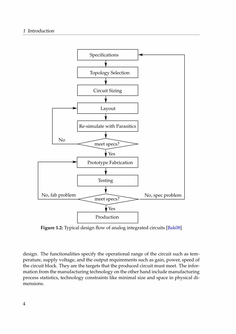
In the context of this thesis, the focus is on the methodology of design and analysis ofthe analog part of the integrated circuits. A typical analog integrated circuit designflow, consisting of several steps and loops [Bak08], can be summarized in Figure 1.2.
The input of the flow are the specifications. They describe the functionalities of thecircuit, as well as the information from the manufacturing technology needed for the
3
1 Introduction
Specifications
meet specs?
Testing
Yes
Prototype Fabrication
Layout
Re-simulate with Parasitics
No
No, fab problemmeet specs?
Production
Yes
No, spec problem
Circuit Sizing
Topology Selection
Figure 1.2: Typical design flow of analog integrated circuits [Bak08]
design. The functionalities specify the operational range of the circuit such as tem-perature, supply voltage, and the output requirements such as gain, power, speed ofthe circuit block. They are the targets that the produced circuit must meet. The infor-mation from the manufacturing technology on the other hand include manufacturingprocess statistics, technology constraints like minimal size and space in physical di-mensions.
4

1.2 Analog Design
The next step is the topology selection, which remains one of the most creative taskfor a circuit designer who has to select the appropriate device types and connectionsto achieve the specifications. This selection is mostly based on the experience of thedesigner.
Then, for the selected circuit topology, the device parameters, such as transistor di-mensions, values of resistors and capacitors, and so on, have to be tuned properly inorder to meet the specifications and to increase the robustness over variations in themanufacturing process and the operational environment. This step is called circuitsizing. This step is performed in a looped manner such that the designer must checkthe simulation results after they make adjustments to certain device parameters.
The steps until now are also referred to as the frontend of the analog design process.Then, the next steps belong to the backend part.
If all of the pre-defined specifications are fulfilled, now it comes to the step of layout,generally performed by layout designers. The placement and interconnections ofeach device on the chip over different layers are determined at this step. Once thelayout is done, parasitic parameters such as strap capacitance and leakage can beextracted and calculated. Re-simulations with these parasitics are necessary. Thisstep is repeated until all specification are met considering layout parasitics.
The next tasks are moved onto fabrication. At first, prototype chips are fabricated andtested. Then any encountered fab problem is fixed. If at this stage the performance offabricated chip cannot meet the requirements and it is not a fab problem, a redesignfrom the first step has to be performed, which is obvious a huge waste of time andinvestment.
Finally, when the chip meets all the specifications, it is ready for production.
1.2.2 Discussions and Challenges
One observation from the above typical analog integrated circuit design flow is thatthe designed circuit performances are subject to many influential factors, especiallythe influences due to the uncertainties during circuit operation in real-time, as wellas the imperfectness during the manufacturing process.
Although beyond designers’ control, those influential factors must be well consid-ered by designers during the design step. The circuit must meet the specificationsunder the maximal tolerance region of uncertainties from operational conditions andprocess variations, otherwise several redesign loops are needed, as can be seen in
5

1 Introduction
Figure 1.2. Such redesign loops should be kept as few as possible, since they result inan increase of overall costs and decrease of the time to market.
One typical solution for designers to meet those requirements is to separate their de-sign/sizing process into several steps, such as nominal design and design centering.During the nominal design step, no tolerance region is considered. It is mainly usedfor the architecture investigation, served as the starting point for the design center-ing as well. During design centering, the tolerance region of process variations andoperational conditions are considered. Certain mathematical models are built up fordifferent uncertainty sources. The designers then refine their design with considera-tion of the uncertainties by the help of those mathematical models, in order to makesure that their circuit can meet all the specifications under all circumstances.
Another observation from the analog design flow is that, in contrast to the digitalpart, the above analog design flow is mostly done manually. The analog design au-tomation is generally available only for the circuit simulation step.
From the design of the circuit to the circuit layout, most of the steps in the analogcircuit design flow still require experience from designers and layout engineers. Asthe circuit complexity grows and many challenges arise as discussed in Section 1.1, itis pointed out by numerous studies that the analog parts of the chip design are mostfrequently at fault when chips fail at first silicon [BC10]. It means a huge re-designcost, if the initial design cannot meet specifications considering possible side effectsand challenges. Thus new methodologies for analog design automation are neededconsidering effects such as process variations and lifetime parameter degradations.
1.3 Contributions of this Thesis
1.3.1 Study on Joint Effects of Process Variations and TransistorAging
This thesis studies deeply the joint effects of manufacturing process variations andtransistor aging. The state-of-the-art methods for design centering considering pro-cess variations, and solutions towards transistor aging are studied thoroughly. Thephysical modeling and behavior as well as the impact of various transistor aging is-sues are focused. The general problem of the joint effects is formulated analyticallyas optimization problems.
6

1.3 Contributions of this Thesis
1.3.2 Design Flow for Lifetime Robustness Optimization
This thesis extends the formulations and applications of the so-called worst-case dis-tance, which is a measure of the design robustness over process variations and op-erating conditions, into reliability modeling and optimization considering transistoraging over lifetime. The aged worst-case distance in lifetime can be used to study theaged yield value.
A new design flow is proposed to optimize the lifetime robustness of analog circuits,by optimizing the fresh circuit with the checking of both fresh and aged sizing rules,as well as maximum layout area constraints, to achieve x-sigma robustness in circuit’slifetime. Then the lifetime robustness of the circuit is analyzed by the evaluation ofaged worst-case distance values.
By applying the design flow repeatedly with different maximum area constraints,the trade-off between circuit’s lifetime robustness and the price we pay in terms ofthe circuit layout area can be obtained. Circuit designers can choose from differentproduct reliability categories with an acceptable area overhead.
1.3.3 Analytical Modeling for Aged Yield Prediction
This thesis proposes a modeling and prediction framework to predict the aged worst-case distance value and the corresponding lifetime robustness of analog circuits. Theproposed method is based on the sensitivity analysis of transistor parameters overaging, as well as the sensitivity analysis of the circuit robustness over transistor pa-rameters.
It does not involve either analytical formulation of circuit performance or Monte-Carlo simulations. In comparison to the aged yield analysis based on the geometricalyield modeling, the proposed method is more efficient in obtaining the aged worst-case distance values.
Using the proposed method, circuit designers can obtain quickly an overview of thelifetime robustness of their design, since the fresh worst-case distance is already avail-able for a fresh-optimal design. Certain weakness in the lifetime robustness of theirdesign can be obtained early and quickly, thus reducing the redesign cost.
7

1 Introduction
1.4 Previous Publications
During the past four years, parts of the work presented here were published in[GP09], [PG09], [PG10b], [PG10c], [PG10a], [PG11a], [PG11b] and [PG12]. A two-step reliability optimization flow involving a fresh yield optimization step for thefresh circuit and a lifetime yield optimization step for the aged circuit was detailedin [GP09] and [PG09]. Its software demonstration was presented in [PG10a]. To speedup the analysis of the aged yield value of the circuit, a linear approximation modelwas introduced in [PG10b], while in [PG10c] several improvements were detailed.The layout area cost for the reliable design was presented in [PG11a]. In [PG11b] thedetailed trade-off between circuit reliability and layout area cost was analyzed. Animproved version with study into each transistor area and circuit performance waspublished in [PG12].
1.5 Organization of this Thesis
The rest of the thesis is organized as follows. Chapter 2 discusses in detail of thereliability issues of the modern analog integrated circuit design process. Chapter 3gives the problem formulation of the work presented in this thesis. Special focus ison the formulation of both fresh and aged yield on different design spaces, as wellas the fresh and aged sizing constraints. The analysis and requirements concerningstatistical analysis methods are discussed in detail. Chapter 4 studies the problem ofrobustness optimization by fresh yield optimization with consideration of both freshand aged sizing rules. The fresh circuit is over-designed such that it is tolerant ofboth process variations and transistor aging. Then Chapter 5 proposes an analyticalprediction model based on sensitivity analysis to approximate the aged worst-casedistance value and its corresponding aged yield. The model can be used to predictthe age of the circuit as well, providing the acceptable aged yield value as the input.The experimental results on different circuitries using industrial models are given inChapter 6. Finally Chapter 7 concludes the thesis.
1.6 Summary
The continuous scaling of semiconductor technology into nanometer scale con-tributes to the higher chip densities, circuit performances, lower cost per transistor,as well as several challenges and side effects, which will limit the product yield value
8

1.6 Summary
after manufacturing and in circuit lifetime. Among those hazards, most influentialproblems arise from manufacturing process variations and transistor degradation re-lated lifetime circuit reliability.
The thesis concentrates on the sizing methodology solutions to the joint effects ofprocess variations and transistor aging. New modeling and prediction frameworkwill be introduced in the thesis.
9


Chapter 2
Reliability Issues
This chapter presents in detail the reliability issues studied in the thesis. The reliabil-ity issues in general relate with the uncertainties of the produced circuits in operatingtime, in comparison to the figure of merit specified during design time. Section 2.1covers the manufacture process induced variations and the resulting uncertainties ofthe manufactured circuits. Section 2.2 introduces the important degradation effectsoccurred in operating time. Section 2.3 introduces and discusses about the current so-lutions in solving manufacturing process variations and transistor aging problems.
2.1 Process Variations
The modern semiconductor manufacturing normally consists of series of processingsteps. From now on we focus on the CMOS technology as it is used in most VeryLarge Scale Integrated (VLSI) or Ultra Large Scale Integrated (ULSI) circuit chips[Bak08]. Typically those processing steps are performed on ultrapure, defect-freeslices of silicon wafers, and photolithography is used repeatedly to build up variousfeatures on different locations through multiple layers on the surface of the wafer.
The variations induced during the manufacturing process can be both systematic andrandom [Nas08]. The systematic variations, or intra-die variations, refer to those vari-ations occurring repeatedly over many chips or wafers, i.e., at system level. Exam-ples of the systematic variations can be wafer-level variations due to layout-inducedstrain, optical-proximity correction [Sah10], the rapid ramp-rate of the lamp thermalannealing process [ea06], etc. The random variations or inter-die variations, on theother hand, refer to the fluctuations which happen in a statistical manner during themanufacturing process such as thermal oxidation, doping process, etc. Examples of
11

2 Reliability Issues
random variations can be random discrete doping, line-edge roughness, line-widthroughness, interface roughness [Sah10], etc. They contribute to the variations of eachtransistor’s threshold voltage or oxide thickness, and so on.
In comparison to the systematic variations which can be addressed either by makingchanges to the design or by improvements in the manufacturing process, the randomvariations can only be tolerated if the initial design has enough margins built by thedesigners. In other words, the designers have to consider during the design phasethe worst case scenario that may happen during the manufacturing process to ensurethat the circuit can work properly under process variations.
2.2 Reliability
2.2.1 Reliability Function R(t) and Failure Rate z(t)
In traditional reliability engineering, Reliability Function and Failure Rate are two veryimportant indicators of the device reliability properties. The study presented in thisthesis is closely linked to the evaluation and approximation of the reliability functionand failure rate of analog integrated circuits. While detailed discussion will be pre-sented in later chapters, here some basic introduction and definitions regarding thesereliability engineering terms are given.
The term Reliability is defined as the probability that a device will function withoutfailure over a specified time period or amount of usage, according to the IEEE Stan-dard Dictionary of Electrical and Electronic Terms [RI97].
Here, the term amount of usage refers to those kinds of one-shot items, such as elec-tronic fuses, safety matches, etc., the usage of which can be divided into two phases:a non-active phase and an active phase. Since analog circuits mainly operate contin-uously, we focus our discussion only on the continuous operation devices hereafter,i.e., the term a specified time period is of interest here.
The reliability thus can be defined as follows. Assume the lifetime of a device is arandom variable, denoted by X, and its cumulative distribution function F(t) corre-sponds to the probability that X will not exceed a certain t, i.e., F(t) = prob(X ≤ t)Then, the reliability of the device, denoted by R(t), is
R(t) = prob(X > t) (2.1)= 1− F(t) (2.2)
12

2.2 Reliability
R(t) is the so-called Reliability function, while F(t) is the so-called lifetime distributionfunction [BJ77]. The above definition comes from the fact that the reliability of a deviceat time t is also the probability that the lifetime of the device will exceed t. In otherwords, 1 − R(t) equals the value of the lifetime distribution function at t. Threeobservations from (2.2) can be made:
1. when t = 0, R(0) = 1;
2. when t→ ∞, limt→∞
R(t) = 0;
3. R(t) must be an non-increasing function of time t.
The first observation implies an important assumption that, at t = 0, all of the devicesare just manufactured and all of them can work properly. At this time, no aging effecthappens, and no transistor parameter drifts due to reliability issues. The secondobservation can be stated also as all of the devices have their maximum lifetime,beyond which they will not work properly any more. And the last observation comesfrom the definition of R(t).
The failure rate z(t), on the other hand, comes from such a probability evaluation.Considering a small time interval between t and t + dt, the product z(t)dt is thus theprobability that a device is failed during this time interval dt, given the condition thatit works properly at least until t:
z(t)dt = prob(t < X < t + dt|X > t)
=prob(t < X < t + dt)
prob(X > t)
=F(t + dt)− F(t)
R(t)(2.3)
z(t) can be obtained if (2.3) is divided by dt:
z(t) =F(t + dt)− F(t)
dt· 1
R(t)=
f (t)R(t)
(2.4)
where f (t) is the lifetime probability density function, defined as
f (t) =dF(t)
dt(2.5)
= −dR(t)dt
(2.6)
The failure rate z(t) is also known as hazard rate, or hazard.
13

2 Reliability Issues
The relationship between R(t) and z(t) can be obtained from (2.4). Since
z(t) =f (t)R(t)
=−dR(t)/dt
R(t), (2.7)
we can get R(t) by integration:
R(t) = exp[−∫ t
0z(ξ)dξ
](2.8)
Infant Mortality
Useful Life
worse
Failure Rate
time
time
Reliability Function
Wearoutworse
Figure 2.1: The Bathtub Curve with effects of the device increasing wearout degrada-tions.
The typical reliability curve is the so-called bathtub curve [BJ77], [KKW03], [Hjo80], asshown in Figure 2.1. The name bathtub comes from the shape of the failure rate curvez(t) in the lower part of Figure 2.1.
Three typical regions can be identified in Figure 2.1.
14
2.2 Reliability
• The first is the "infant mortality" period, during which the devices may fail dueto initial weakness or defects. The failure rate of this period often drops quickly,until reaching a relatively constant level.
• Now it is the second period when the devices are in their useful normal operatinglife. In this period the failure rate is approximately constant and very small. It isalso called intrinsic failure period. As the time proceeds, the devices graduallydegrade due to various aging effects.
• Then the system enters the last period, the wearout period. The failure rate ofthis period is increasing, and the whole system gradually reaches the end of itsuseful lifetime.
An example function concerning R(t) and z(t) is from exponential distribution,which is useful when approximating R(t). In this case, the lifetime distribution func-tion F(t) is 1− e−λt, where λ is a positive constant. According to (2.2) and (2.7), R(t)and z(t) can be expressed as
R(t) = e−λt (2.9)z(t) = λ (2.10)
where the failure rate z(t) remains constant during the useful lifetime of the product.
Also shown in Figure 2.1 are the effects which may worsen the device reliability dueto increasing aging effects, as can be seen on the dotted lines. Such degradation mayhappen early during the device normal lifetime, causing the failure rate to increaseeven during the designed useful lifetime of the devices. As introduced in the follow-ing, such problem is getting worse as the semiconductor technology continuouslyscales.
Some of the most important degradation effects on transistors and on-chip intercon-nects are reviewed in the following sections. Their impacts on the transistor param-eters or on the interconnects are discussed. For a more complete discussion, pleaserefer to [HTH+85], [SB03], [AKVM07], [WRK+07], [WSH00].
2.2.2 Negative Bias Temperature Instability
The physical behavior of Negative Bias Temperature Instability (NBTI) on a PMOStransistor is shown in Figure 2.2. As the name indicates, NBTI manifests itself whenthe PMOS transistor is "negative" biased, i.e., Vgs < 0. It is commonly acceptedthat NBTI is the result of hole-assisted breaking of Si-H bonds at Si/SiO2 inter-
15

2 Reliability Issues
face [AKVM07] when a PMOS is negative biased using the Reaction-Diffusion (R-D)model:
dNIT
dt= kF(N0 − NIT)− kRNH(0)NIT (2.11)
where NIT is the fraction of Si-H bonds at the Si/SiO2 interface which breaks at timet, N0 is the initial number of all Si-H bonds, and kF is the dissociation rate constant.The second term in (2.11) describes the annealing process of the released H atoms.NH(0) is the H concentration at the interface.
n- Substrate
HH
...Si Si SiSiSi Si Si Si
p+ p+
Gate
DrainSource
HH H H H H
...
Oxide
Figure 2.2: Effects of NBTI
NBTI is getting more serious as technology scales, since the vertical oxide field is con-tinuously increasing to enhance transistor performance. Thus a hole in the channelcan be easily captured and a two-electron Si-H covalent bond at the Si/SiO2 interfacecan be weakened by it. The weakened Si-H bonds break easily at certain high tem-perature. Atomic H’s are released in short time, then they convert to and diffuse asmolecular H2 in long time (>100 s) [AKVM07].
NBTI effect will degrade certain transistor parameters, such as threshold voltage,drain current, transconductance, etc. Threshold voltage degradation due to NBTI isgiven by [YQD+09]
4Vth = A(
Vgs
tox
)α
exp(− Ea
kT
)tn (2.12)
where K is Boltzmann’s constant, A is a process related prefactor, Ea is the activationenergy, α denotes voltage acceleration factor, n = 1/4 for atomic H in short time, andn = 1/6 for molecular H2 in long time as discussed above.
16

2.2 Reliability
A well known effect of NBTI on PMOS transistor is its partial recovery, or annealing,when the stress is removed [CCL+03], [RMY03]. Several studies on the modelingof this dynamic behavior and its application in the design of digital circuits are pre-sented in [VWC06], [LWH+07]. For SRAM cell, the impact of fast-recovering NBTIdegradation is studied in [DHGSL10]. But for analog circuits, the NBTI recovery isnot obvious [JRSR05]. The reason for this is the presence of the constant DC bias-ing voltage in the most of analog circuits, which leads to a continuous stress voltageapplied on the transistors in analog circuits. Such continuous stress voltage is not de-pend on the input signals. As a result, NBTI recovery or annealing is a minor effectfor analog circuits and will be ignored in the rest of this thesis.
The intrinsic variations of NBTI effects are studied in [Rau02]. The expression ofvariation in4Vth shift is
σ(4Vth) =
√Ktoxµ(4Vth)
AG(2.13)
where tox is effective gate oxide thickness, AG is its area and K is an empirical con-stant. As tested by authors in [FAH+08] and [FAH+09], for the transistor parametersVth and Id, their probability density functions follow a Gaussian distribution pre andpost NBTI stress.
It is pointed out in [SB03] that, NBTI should not exhibit any gate length dependence,since it does not depend on lateral electric fields. But NBTI is sometimes enhancedwith reduced gate length, which is not well understood yet. The closeness of thesource and drain maybe one of the reasons for that.
The introduction of new dielectric material, such as high-κ gate dielectrics (with highdielectric constant κ compared to silicon dioxide), is one of several strategies devel-oped to allow further shrinking recently [wika]. But at the same time, a so-calledPositive Bias Temperature Instability (PBTI) effect on a NMOS transistor occurs asthe transistor degrades over time if the NMOS transistor is biased positively.
Recently a reliability assessment of voltage controlled oscillators in 32nm high-κ,metal gate technology is presented in [CFSL10] with aging behavior assessment dueto NBTI on PMOS transistors and PBTI on NMOS transistors. A detailed study intothe impact of analog circuit operations is presented later in [CMFSL11b]. Anotherstudy of NBTI and PBTI effects on 6T SRAM memory cell is presented in [DGSL09],showing the significant impact of process variations, NBTI and PBTI on future tech-nologies with new material.
17
2 Reliability Issues
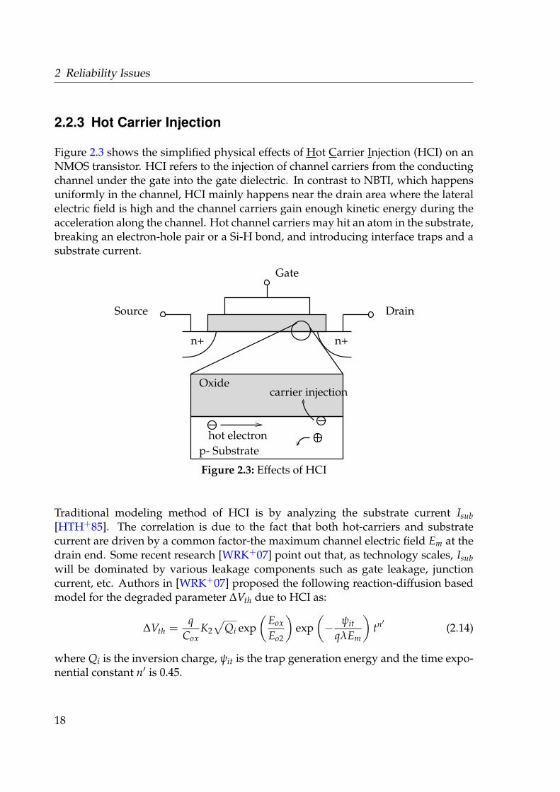
2.2.3 Hot Carrier Injection
Figure 2.3 shows the simplified physical effects of Hot Carrier Injection (HCI) on anNMOS transistor. HCI refers to the injection of channel carriers from the conductingchannel under the gate into the gate dielectric. In contrast to NBTI, which happensuniformly in the channel, HCI mainly happens near the drain area where the lateralelectric field is high and the channel carriers gain enough kinetic energy during theacceleration along the channel. Hot channel carriers may hit an atom in the substrate,breaking an electron-hole pair or a Si-H bond, and introducing interface traps and asubstrate current.
hot electronp- Substrate
carrier injection
Gate
DrainSource
n+ n+
Oxide
Figure 2.3: Effects of HCI
Traditional modeling method of HCI is by analyzing the substrate current Isub[HTH+85]. The correlation is due to the fact that both hot-carriers and substratecurrent are driven by a common factor-the maximum channel electric field Em at thedrain end. Some recent research [WRK+07] point out that, as technology scales, Isubwill be dominated by various leakage components such as gate leakage, junctioncurrent, etc. Authors in [WRK+07] proposed the following reaction-diffusion basedmodel for the degraded parameter ∆Vth due to HCI as:
∆Vth =q
CoxK2√
Qi exp(
Eox
Eo2
)exp
(− ψit
qλEm
)tn′ (2.14)
where Qi is the inversion charge, ψit is the trap generation energy and the time expo-nential constant n′ is 0.45.
18

2.2 Reliability
2.2.4 Time-Dependent Dielectric Breakdown
Time-Dependent Dielectric Breakdown (TDDB) is a reliability issue of the transistorgate oxide. As the technology scales, the thinner gate oxide and the stronger electricfields across the gate oxide can damage the oxide in such a way that the transistorgate current increases, resulting in a totally loss of the isolating property of the gateoxide [WSH00].
There are two types of the dielectric breakdown: soft break down (SBD) and hardbreak down (HBD). Depending on the number of positions where an increased localgate current occurs, SBD manifests itself as an increase of the leakage current. Whenthe number of such positions and the resulting random traps inside the oxide reachea certain limit, HBD occurs such that the oxide isolating property is completely lostand a percolating path through the oxide will short the gate to the substrate, resultingin a transistor failure [GDWM+08]. The time to HBD can be modeled by a Weibulldistribution.
As pointed out in [AWS02], the breakdown of oxides stressed at operating voltages(1.0V-1.5V) can "never be" hard. In addition, authors in [AVK08] show that as supplyvoltage reduces, the transistor can maintain functional under several SBD paths inthe oxide. The positions of SBD paths in the oxide have significant influence here.
2.2.5 Electromigration
Electromigration problem is the reliability issue of the on-chip interconnects [TR07].In modern technologies, the on-chip interconnects are very thin and narrow. Sucha small cross section area of the interconnects will increase the current density thatflows through it, which means a movement of a huge amount of electrons. The elec-tron movements then can interact with the metal ions in the interconnects and re-place them. As a result, "voids" and "hillocks" are formed in the interconnects. Theformer, a vacancy area of metal ions, can cause open circuit, or in other words ex-tremely large resistance in the interconnects, corresponding to a failure event, whilethe latter, locally accumulated metal ions, can cause short circuit between neighbor-ing interconnects, resulting in a malfunction of the circuit.
Electromigration is a reliability effect that must be taken care of during layout phase.Certain interconnects must be widened where current will be high in the operation.Some special layout techniques, such as Slotted Wires, can be applied as well [Lie06].
19

2 Reliability Issues
2.3 State of the Art
2.3.1 Reliability Simulation
Starting from the early 1990’s, microelectronic system reliability problems, such asHCI, TDDB, raised due to the rapid advances of fabrication technologies and theemerging VLSI circuits at that time. Several reliability simulators based on softwareprograms were proposed in academia as well as in industry to help the designersgain more insights into their design quality.
• Sheu et al. from the University of Southern California, proposed the simulatorRELY [SHL89], which simulated the HCI effects based on the substrate currentmodel.
• Leblebici et al. from the University of Illinois at Urbana-Champaign proposed asimulation framework considering the dynamic behaviors of HCI, by solving ofa set of differential equations at t to obtain the interface trap densities and thusthe transistor damage at that time [LK89].
• Hu et al. from the University of California at Berkeley proposed the reliabilitysimulation tool BERT [Hu92], which enclosed several modules for different agingeffects.
• From industry side, Texas Instruments proposed HOTRON [AHY87] for HCI ef-fects simulation. Philips (later known as NXP) proposed PRESS [LWM+93] forHCI effects simulation.
Entering early 2000’s, with the ever shrinking of the device feature size and theemerging of new aging effects such as NBTI, the reliability modeling and simula-tion again attracted the attention from various communities. [LMM06] presented therecent available EDA tools to simulate the HCI, NBTI and Electromigration effects.
• One of the major commercial tool RelXpert from Cadence Design Systems basedon BERT was presented in [LMM06]. The general workflow of RelXpert is shownin Figure 2.4. The prebert and postbert are the internal processors during theaging simulation. The detailed aging simulation using RelXpert is presented inSection 4.3.1.
• The implementation of HCI simulation in another commercial simulator Eldofrom Mentor Graphics was described in [KFHR01], where the new .AGE com-mand calls repetitive simulations to obtain an accurate prediction of the circuitdegradation with dynamic operating conditions. The workflow of such repeti-tive simulations is shown in Figure 2.5. Inside such a flow, the target time point
20

2.3 State of the Art
Aged Circuit Netlist
RelXpert
Aged Device
SimulatorCircuit
Fresh Circuit Netlist Reliability Parameters
prebert postbert
Figure 2.4: General workflow of RelXpert
Tage is divided into n smaller intervals Tl. The circuit is simulated at the end ofeach time intervals, such that the gradual change of bias conditions as a result ofthe transistor degradation can be simulated.
• The simulator ARET from Georgia Institute of Technology was presented in[XCS+03]. It can handle HCI and Electromigration simulations. For Electromi-gration effects, the probability of certain post-fabrication defects on interconnectsare obtained based on statistical models.
• Li et al. from the University of Maryland introduced another reliability simulatorMaCRO in [LQH+06]. MaCRO can simulate HCI, NBTI and TDDB by substitut-ing the degradation-sensitive transistors with failure-equivalent circuit models,such that a large number of circuit simulations on small time intervals can beavoided.
2.3.2 Solutions towards Transistor Aging
There are several methods in literature trying to solve the transistor aging issue. Theyincludes initial over-design [KKAR06], smart clock tree signaling [CGRP09], in-situmonitory circuitry [Die07], [QS08], as well as the using of chopper stabilization andautozeroing [MFCSL11].
• Authors in [KKAR06] propose a gate sizing algorithms for digital circuits to ini-tially over-design the circuits. They first calculate the Vth degradation for eachtransistor assuming signal probability for the gate inputs. Then they size the
21

2 Reliability Issues
Calculate
(t = nTl)
Fresh Simulation
age-Table
Aged Simulation
t = Tage?
n++
End
No
Yes
Figure 2.5: Repetitive simulation workflow of ELDO
gates assuming the intended lifetime and the calculated Vth degradation, thusachieving a degradation-aware gate sizing. As pointed out by various commu-nities, over-design is straightforward to account for reliability issues. The over-design solutions rely on efficient algorithms to minimize the area overhead whileachieving the expected product lifetime reliability.
• Authors in [CGRP09] propose design techniques with low overhead to overcomethe NBTI induced skew degradation of clock tree, using a so-called Gating withBoth Logic Value (GBLV) scheme. They observe that the PMOS transistors inclock buffers experience alternating stress and recovery stages of NBTI duringswitches of the clock signal in every cycle. The PMOS transistors in gated clocktrees, on the other hand, do not experience such alternating cycles, since thatpart of the clock tree is shut down by the clock-gating. They generate an auxil-iary signal AUX alternating between low and high values, thus balancing NBTIdegradations among various clock buffers.
• Authors in [Die07] review the idea of applying additional monitors to the circuitsand additional knobs to countermeasure the degradation and other side effects.
22

2.3 State of the Art
The solution can be in both circuit level down to hardware and system level upto intelligent software algorithms to control the circuit behaviors.
• Authors in [QS08] propose an in-situ monitor circuitry to track the effects of NBTIand mitigate the degradation in real time using an adaptive body biasing schemeby forward-biasing the PMOS transistors under stress. Applying the output volt-age of the monitor circuitry directly to the body of the PMOS transistors understress, the tolerance of ∆Vth increases in comparison to a PMOS transistor withbody connected to Vdd as in normal cases. The deploying of such monitor cir-cuitry, however, turns out to be another trade-off between the additional layoutarea and the measurement accuracy, since it is impossible to deploy the moni-tor for each PMOS transistor under stress. In practice one monitor circuitry isallocated for a group of neighboring transistors to reduce area overhead and theinfluence of local process variations.
• Authors in [MFCSL11] apply chopper stabilization and autozeroing to reduce theeffects of transistor aging on circuit level. The methods were originally developedto reduce the offset and low frequency noise. By applying chopper stabilization,the input low frequency noise can be shifted to high frequencies which locateoutside the baseband, and the input differential pair are stressed equally resultingin a symmetrical degradation of the transistor pair. By autozeroing technique, onthe other hand, the total stress time of the input pair is reduced by one half, sincethe amplifier operates in close and open loop in an alternative manner.
None of these solutions considers also the manufacturing process variations. Theirmethods rely only on the nominal value of circuit parameters, which cannot ensure arobust design over process variations.
2.3.3 Design Centering considering Process Variations
On the other hand, considering process variation effects only, design methodologiestowards a robust design tolerant of such process variations have been widely studiedduring the last 30 years. In these so-called design centering problems, an optimal setof circuit parameters are assigned to optimize the yield for an assumed statistical dis-tribution of process variations. The approaches of design centering can be classifiedinto two categories: statistical methods and deterministic methods.
2.3.3.1 Statistical Methods
The feature of the statistical methods is the statistical yield analysis using Monte-Carlo simulations [HH64], [Sch66]. The necessary information about the circuit is
23

2 Reliability Issues
collected through those simulations. Based on the Monte-Carlo analysis result ofthe yield value, the yield can be optimized with the formulations of its gradient andHessian matrix with respect to the statistical parameters. A variety of techniques andmethods concerning the efficiency of Monte-Carlo analysis as well as the statisticalyield enhancements are proposed.
Importance sampling [SSG97] is a technique using a different sampling distributionfrom the statistical parameter distribution to estimate the yield with improved esti-mation quality. It is applied widely in several methods such as [HLT83], [STPW76],[SP81] and [SR85].
• Authors in [HLT83] propose a stratified sampling method, where the Monte-Carlo simulations are performed in several disjoint subregions of the originalparameter perturbation region. The total sample size is reduced by emphasiz-ing the samples in the region where the performance specifications are met. Thismethod is similar to a regionalization method proposed by authors in [STPW76].
• Authors in [SP81] propose a parameter sampling method, where the informa-tion in a single run of Monte-Carlo simulation is reused to derive several yieldestimations before being updated.
• Authors in [SR85] propose a control variate technique consisting basically twoMonte-Carlo experiments. First a control run is done consisting a small numberof samples, used to estimate the yield difference between the main circuit and itssimulation-cheaper shadow model. Then an auxiliary run with a larger samplesize is done to estimate more accurately the yield of the shadow model. The yieldof the main circuit can thus be obtained by the results of these two Monte-Carloanalysis.
Another category of the statistical approaches is the statistical experiment-based,such as response surface method. The basic idea is to build up a quadratic modelof the circuit performance, and fit the model parameters via a number of samples onthe response surface of the circuit. Such model then can replace the original circuit insimulations for a fast yield estimation and enhancement.
• Authors in [YKHT87] propose an average mean-squared error criterion to selectan optimal set of circuit simulations in order to derive an accurate performancemodel.
• Authors in [PH93] develop a statistical regression procedure to estimate the re-sponse function of the circuit performances, where the higher order terms areadded selectively to improve the accuracy. The yield is then maximized bypseudo objective function substitution method (POSM).
24

2.3 State of the Art
• More recently, authors in [LFJG09] propose a new stop criterion during the evolu-tionary computation based yield optimization to reduce the number of iterations.They monitor both the average improvement in the whole population of sam-ples and the improvement in the best objective function value. The former part isimportant especially at the beginning of the algorithm to avoid wrong detection,while the latter part is important especially at the final stage of the algorithm tobetter locate the local optimal.
• Authors in [LFG10] further reduce the computational effort in each iteration byallocating the computing budget to each candidate in the population in an opti-mized manner. They identify those critical candidate solutions through an ordi-nal optimization problem, allocating enough number of samples to the Monte-Carlo simulation of these solutions, in comparison to the few samples allocatedto non-critical solutions.
The advantages of the above-mentioned statistical methods are the yield estimationaccuracy in comparison to the deterministic methods discussed below. The maindrawbacks of the statistical methods include the high simulation efforts, which arereduced for the deterministic methods discussed below.
2.3.3.2 Deterministic Methods
The deterministic methods, as its name implies, optimize the yield by approximat-ing and maximizing the acceptance regions, or by building up and maximizing therobustness measures, in a deterministic manner, i.e., based on sensitivities calculationin stead of a number of random samples as in the statistical methods. Then designcentering is performed such that either the center of the approximated acceptanceregion is found, or the robustness measures are maximized.
The acceptance region is defined either on the performance space or parameter space,where the part of the circuit realization after manufacturing process can meet all per-formance specifications. The exact definition and formulation is detailed later inChapter 3. Authors in [BGT81] propose the ellipsoidal method, where the yield ismaximized by maximizing the volume of the ellipsoid that is inscribed by the accep-tance region. Since the acceptance region itself is nonlinear in most cases, its shape istoo difficult to determine. So several other papers make simplification for the shapeof the acceptance region.
• Authors in [SPV99] use advanced first-order second moment (AFOSM) methodto approximate the yield, where the acceptance region is approximated by a poly-hedral. The yield is maximized by finding the maximum-volume norm body
25
2 Reliability Issues
contained in the approximated polytope. The authors also propose a unifiedframework for different design centering task such as tolerance design, worst-case disign, process design, etc., by selecting appropriate norms.
• Authors in [WVO97] replace the single ellipsoidal approximation of the accep-tance region by piecewise second-order functions, so-called piecewise ellipsoidalapproximation (PEA). The second-order derivative of the constraint is from theboarder region, i.e., the ellipsoid that matches the constraint region. Then, this in-formation is inserted into the second-order Taylor series expansion in the neigh-borhood of the nominal value. They show this mixed construction is accurate foryield optimization problem.
• Authors in [PSV01] approximate the acceptance region by a general polytope.The yield is then optimized using convex programming approach with an esti-mation of the yield gradient.
• Authors in [DH77] approximate the acceptance region by a simplex, the numberof which is extended in every iteration during yield optimization. The yield isthen optimized by finding of the center of the largest hypersphere inscribed intothe convex hull of all approximating simplex.
• Authors in [AMHH99] improve the speed of convergence of the ellipsoidal tech-nique by using double-sided ellipsoidal section. The double-sided ellipsoidal isbounded by two hyperplane, the first of which is built up by linearization of theacceptance region boundary at one boundary point, the second of which is foundby determining a boundary point at which the gradient of the boundary of theacceptance region is opposite to that of the first hyperplane.
The other type of deterministic optimization methods is building up and maximizingcertain robustness measures.
• Authors in [AGW94] propose the formulation of the worst-case distance, whichis defined to be the distance between a performance specification and the meanvalue of that performance in terms of a number of standard deviations. Thestandard deviation of a performance is formulated by the attributes of statisti-cal parameters which have underlying statistical distribution during manufac-turing process. The analysis and optimization of worst-case distances thus areequivalent to the analysis and optimization of the circuit robustness over processvariations. A sequential quadratic programming approach is proposed in [Sch03]to solve that optimization formulation. This thesis further extends the idea of theworst-case distance into the time domain. The methodologies of analysis andoptimization considering the aged worst-case distance after transistor aging areproposed. The first- and second-order sensitivities of the worst-case distance over
26
2.3 State of the Art
time are derived for the first time, enabling a quick prediction of the aged worst-case distance based on Taylor expansion.
• Authors in [KD95] use a linearized performance penalty (LPP), which is the per-formance model linearized over the mean value of the statistical parameters. Theevaluation of such model requires only one circuit simulation without using aniterative optimization algorithm, with a trade-off over the accuracy.
• Authors in [DK95] optimize the worst-case performance to increase the totalyield, where the performance is built up by a response surface model. It is not ex-actly a design centering approach, but a method to find a design with predefinedworst-case performance, i.e., the worst-case robustness.
• Authors in [AS94] and [DG98] make use of the capability indices Cp and Cpk,which originate from process control. Cp measures how "narrow" the perfor-mance distribution is (the variability part), while Cpk measures the distance be-tween the mean value and the most critical performance specifications (the cen-tering part). Their methods are based on new target functions, combining theabove two indices, such that the variability can be minimized and design can becentered. The method in [AS94] builds up response surface models for the per-formances, while the method in [DG98] makes symbolic equations for the perfor-mances.
2.3.4 Joint Effects of Transistor Aging and Process Variations
It is only since very recent years that the joint effects of process variations and lifetimeparameter degradations are studied [AKPR07]. A various of solutions are proposedin literature. They differ in the type of reliability effects considered and the type ofcircuits studied.
For digital circuits, NBTI-aware statistical timing analysis considering process varia-tions are proposed in [VOXW09], [VOX09], [WRY+08] and [LSZ+09].
• Authors in [VOXW09] build up a gate-level delay fall-out model by propagatingthe device parameter fall-out model due to NBTI and process variations into thegate delay model. To study the joint effects on the circuit level with multiple gatestages, they use HSPICE based Monte Carlo simulations. They consider in addi-tion the intrinsic variations of NBTI process in [VOX09]. A sizing methodologyconsidering the joint effects is not covered in their works.
• Authors in [WRY+08] propose a statistical prediction methodology consideringprocess variations and transistor aging due to NBTI. They study the joint effectson gate level delay by applying the transistor level aging model into a process
27

2 Reliability Issues
variation-aware gate delay model. Then they are able to model the timing behav-ior of a single path considering the joint effects. No sizing solution is proposed intheir work either.
• Authors in [LSZ+09] build up an NBTI-aware statistical gate delay model usingthe stochastic collocation method. They apply their model also into the circuitlevel statistical timing analysis considering various working conditions of thecircuit in runtime. Then they propose a sensitivity analysis framework basedon their NBTI-aware circuit level statistical timing analysis, such that the criticalgates can be identified and optimized during circuit sizing.
All of those methods rely on the analytical expression of performance features suchas delay time, which is suitable for digital circuits but difficult in analog domain.
For analog circuits, various methodologies on the investigation and mitigation of thejoint effects are proposed in [MG09], [MG10], [MG11], [MDJG12] and [CMFSL11a].
• Authors in [MG09] use Monte-Carlo simulation loop to obtain the degraded per-formance values for each fresh random sample at every lifetime point. Then themost appropriate distribution function at each time is fitted, thus a failure distri-bution throughout the lifetime can be found. It results in a high simulation effortand difficulty for further optimization.
• They improve their method in [MG10] using a response surface model to speedup the simulations, where certain numbers of random samples are still requiredto obtain the degraded distribution information. They verify that an initial over-design can improve the lifetime robustness of the circuits. However, a quantifiedsolution is not available from their work to guide the circuit sizing process. Thetemporal stochastic reliability effects are considered in addition in [MG11] usinga similar methodology.
• In [MDJG12], the authors further speed up the simulation on large analog andmixed-signal systems by partitioning of the large system into smaller manage-able subblocks. They use fast function extraction symbolic regression method tocope with the high number of dimensions and the nonlinear circuit behavior. Anactive learning sample selection algorithm is proposed to select optimal modeltraining samples and to limit the amount of expensive aging simulations. Nosizing solution is considered either.
• Authors in [CMFSL11a] propose another technique to suppress the effects of ag-ing and process variations on analog circuits. Firstly a Burn-In phase is appliedwhere the asymmetric open-loop stress conditions are switched into symmetricstress to control the BTI effect in saturation. The symmetric stress is generated byswitching the asymmetric input stress with a 10Hz clocking frequency. Secondly
28

2.4 Summary
a Calibration phase is applied where a selective asymmetric stress is applied totransistors to compensate the offsets caused by process variations. The proposedtechnique allows smaller device dimensions be used in the design, since offsetscan be calibrated after manufacturing.
2.4 Summary
The reliability issues from manufacturing process variations and transistor aging arediscussed in detail. These have been the major concern for both circuit design andchip manufacturing communities for decades, since these will result in yield loss andextra redesign costs.
Most of the previous research consider these reliability problems separately. Al-though there are proposals in solutions towards transistor aging or process varia-tions alone, it is only since recent years that the studies on the joint effects appear.The state-of-the-art studies on the joint effects concentrate on digital circuits, wheredevice parameter variations and aging can be propagated into gate level or circuitlevel performance formulations. For analog counterparts, the studies are still limitedand no sizing solutions are available.
This thesis will study the joint effects of manufacturing process variations and tran-sistor degradation related lifetime circuit reliability in detail, with proposal of newmodels and new design methodologies for analog circuits.
29


Chapter 3
Problem Formulation
This chapter formulates the problem studied in this thesis and gives formal definitionof terms used throughout the thesis.
3.1 Age and Lifetime
In this section, the differentiation between two terms which are used throughout thethesis, age and lifetime, is discussed.
Literally, age is defined as "length of time that a person or organism has been alive;length of time that an object has existed", while lifetime is defined as "span of a per-son’s life, time during which a person is alive; period of time during which somethingfunctions or exists". So for a single person or an object, the value of age is always lessor equal to the value of lifetime, since the lifetime refers to the whole length of thefunctioning period of that person or object.
Similarly, in this thesis, age and lifetime are defined as follows.
First, age, denoted by t, is any point of interest on the time axis. Especially, t0 cor-responds to the time when the circuit is just manufactured without any transistoraging. It can be called as fresh circuit.
Second, given a minimal acceptable yield value, Ymin, the lifetime, denoted by Tli f e,is the time when the aged yield value Y(Tli f e) of a circuit products drops to Ymin. Inother words, at Tli f e, we have
Y(Tli f e) = Ymin (3.1)
31

3 Problem Formulation
The choosing of Ymin will influence the lifetime Tli f e of a circuit products, since theaged yield is a decreasing function over time. If the predefined acceptable Ymin drops,the product’s lifetime will be longer.
Note that the value of Tli f e can be smaller than, equal to or bigger than the value oft, since Tli f e needs a predefined Ymin as an input criteria. In our study t is chosen forany point of interest without a direct indication of the value of Tli f e.
Sometimes people say "lifetime yield", which has the same meaning as "aged yield",i.e., the yield value of an aged circuit. To avoid any misunderstanding, the term "agedyield" is used throughout the thesis.
3.2 Parameters
Parameters of a circuit include all of the contributing factors which influence thebehavior of that circuit. These factors can be fixed values, or random variables. Theycan be from the circuit itself, or from the operating environment. They can drift fromtheir nominal values over time, or remain to be the same amount after manufacturingprocess.
The circuit parameters can be classified into three categories:
• Design parameters, represented by a vector d ∈ Rnd
• Statistical parameters, represented by a vector s ∈ Rns
• Operating parameters, represented by a vector θ ∈ Rnθ
In addition, if time-dependent parameter drifts are considered, as discussed in Sec-tion 2.2, some of the parameters will be a function of age t. Detailed definition anddiscussion are as follows.
3.2.1 Design Parameters
The design parameters d = [d1, d2, . . . , dnd ]T ∈ Rnd correspond to the circuit parame-
ters that the designer can choose during the design phase in order to obtain an "op-timal" design. The examples of design parameters in CMOS circuits are transistorwidths and lengths, nominal values of capacitors and resistors.
For each of these design parameters, there are correspondingly lower and upperbounds. Usually a lower bound is defined by the manufacturing technology, minimal
32

3.2 Parameters
grids, for example, while an upper bound may arise from the limit of the maximalavailable on-chip area. These boundary values can be combined as vectors: dL forthe lower bounds and dU for the upper bounds. Thus a design parameter space D isformed, bounded by an nd-dimensional hypercube:
D = {d|dL ≤ d ≤ dU} (3.2)
In Equation (3.2) and the rest of the thesis, the vector inequality is defined as follows.Assume two vectors x, y ∈ Rnx ,
x ≤ y⇔ ∀i=1,...,nx
xi ≤ yi (3.3)
Since either the transistor dimensions or the capacitor and resistor values will notchange after manufacturing process, we accept the fact that, design parameters dwill not drift over time. They can only be changed during the design phase, beforethe manufacturing process starts. Note that for those manual layout designers, thewidths and lengths of on-chip interconnects are also designable and may suffer fromtime-dependent reliability problem, such as Electromigration (EM). But these effectsare beyond the scope of this thesis. For more complete discussion of on-chip inter-connects reliability problem please refer to [Bla69], [TR07].
3.2.2 Statistical Parameters with Aging
Corresponding to the uncertainty and imperfectness of the manufacturing process,the statistical parameters s = [s1, s2, . . . , sns ]
T ∈ Rns model the variations during themanufacturing, as introduced in Section 2.1. Such variations can be captured usuallyby a statistical distribution. In most cases, the probability density functions (pdf) ofthe statistical parameter distributions are considered.
The types of the statistical distributions vary for different statistical parameters. Forexample, Normal (Gaussian) distribution for the threshold voltage Vth, lognormaldistribution for the oxide thickness tox, etc [Ml95]. These distributions can be trans-formed into Gaussian distribution as shown in [Esh92]. So without loss of generally,the Gaussian distribution are assumed for the statistical parameters throughout thethesis.
For one statistical parameter si, i = 1, ..., ns, it follows Gaussian distribution withmean value si,0 and standard deviation σi. Such distribution can be denoted as
si ∼ N (si,0, σ2i ) (3.4)
33

3 Problem Formulation
The probability density function of si is given by
pdf(si) =1√
2πσi· exp
(− (si − si,0)
2
2σ2i
)(3.5)
For a vector s, the ns-dimensional Gaussian distribution with mean vector s0 andcovariance matrix C, denoted by s ∼ N (s0, C), has the probability density functionas follows:
pdf(s) =1
√2π
ns ·√
detC· exp
(−1
2· (s− s0)
T ·C−1 · (s− s0)
)(3.6)
The level contours of the pdf(s) are ellipsoids:
(s− s0)T ·C−1 · (s− s0) ≡ β2(s) (3.7)
where the covariance matrix C is defined by
C = Σ ·R · Σ (3.8)
=
σ2
1 σ1σ2ρ1,2 · · · σ1σnsρ1,ns
σ2σ1ρ2,1 σ22
. . . ...... . . . . . . σns−1σnsρns−1,ns
σnsσ1ρns,1 · · · σnsσns−1ρns,ns−1 σ2ns
(3.9)
The matrix Σ has all of the non-negative standard deviations σi for every componentof vector s
Σ =
σ1 0 · · · 0
0 σ2. . . ...
... . . . . . . 00 · · · 0 σns
(3.10)
The matrix R has all of the correlations ρi,j between the i-th and the j-th componentof vector s
R =
1 ρ1,2 · · · ρ1,ns
ρ2,1 1 . . . ...... . . . . . . ρns−1,ns
ρns,1 · · · ρns,ns−1 1
, (3.11)
34

3.2 Parameters
where
ρi,j = ρj,i (3.12)−1 ≤ ρi,j ≤ +1 (3.13)
When the transistor aging effects are taken into consideration, certain statistical pa-rameters, such as Vth, will shift their values over time, as introduced in Section 2.2.Thus the vector of statistical parameter can be denoted as a function of age t withaged mean vector s0(t) and aged covariance matrix C(t) as:
s(t) ∼ N (s0(t), C(t)) (3.14)
whose probability density function at that time is
pdf(s(t)) =1
√2π
ns ·√
detC(t)· exp
(−1
2· (s(t)− s0(t))T ·C(t)−1 · (s(t)− s0(t))
),
(3.15)with the level contours as:
(s(t)− s0(t))T ·C(t)−1 · (s(t)− s0(t)) ≡ β2(t) (3.16)
3.2.3 Operating Parameters
The operating parameters θ = [θ1, θ2, . . . , θnθ]T ∈ Rnθ are used to model the influence of
the circuit operating conditions. For instance, supply voltage of the circuit, tempera-ture, capacitive load. These parameters are mostly variable during circuit operations.Such variations are different from that of statistical parameters, since their behaviorcannot be modeled by statistical distributions. In other words, these parameters will"fluctuate" during circuit operations, but will neither have any statistical behavior,nor "degrade" monotonically over time.
The operating parameters are usually bounded by lower and upper bounds, θL andθU respectively. Such boundaries specify the maximal operating range of the circuitunder which the circuit must work properly, for instance, an operational temperaturebetween −40◦C and 120◦C. Thus an operating range Θ is formed, bounded by an nθ-dimensional hypercube:
Θ = {θ|θL ≤ θ ≤ θU} (3.17)
35
3 Problem Formulation
3.3 Performances with Aging
The circuit performance corresponds to the behavior of the circuit. For a typical analogcircuit, such as an operational amplifier, the performances can be gain, slew rate,phase margin, common mode rejection ratio, etc. In practical design, performancesare the output of a numerical circuit simulation. This is in contrary to the circuitparameters, which are usually the inputs of a numerical circuit simulation.
When no time-dependent transistor aging effects are considered, the performancevector f = [ f1, f2, . . . , fnf ]
T ∈ Rnf results from a mapping as follows:
d, s, θ 7→ f(d, s, θ), (3.18)
where all of the circuit parameters, d, s and θ are considered as the contributingfactors of the performance f, and f is called "evaluated" at (d, s, θ).
Thus the performance space F is the set of all possible values of the performance fresulting from the mapping of any possible value of parameter (d, s, θ) in (3.18):
F = {f|f evaluated at (d, s, θ)} (3.19)
f(t2)
s2 f2
f1s1
F
aging agingmapping
s(t1)
s(t2)
f(t1)
Figure 3.1: Mapping from the statistical parameter space onto the performance spaceF considering parameter aging
When the transistor aging effects are taken into consideration, at age t, the perfor-mance vector f(t) = [ f1(t), f2(t), . . . , fnf(t)]
T is evaluated at the vector (d, s(t), θ) as:
d, s(t), θ 7→ f(t)(d, s(t), θ) (3.20)
Figure 3.1 shows qualitatively the aging effects during the mapping from a two-dimensional statistical parameter space onto the two-dimensional performance space
36

3.4 Fresh Yield and Aged Yield
F . As can be seen, at t1, the statistical parameter vector s(t1) maps to the performancevector f(t1), while at t2, after parameter aging, s(t2) maps to f(t2). The aging-inducedperformance degradation thus can change the behavior of the circuit. The changedperformance value may make it not work properly. In Section 3.4 we will see howthis performance degradation influences the aged yield of the circuit.
3.4 Fresh Yield and Aged Yield
3.4.1 Definition
Before introducing the yield, the definitions about performance specification, as wellas the acceptance region on the performance space F and the statistical parameterspace will be discussed first.
Each element fi of f has a certain lower bound and/or upper bound, denoted asfi,L and/or fi,U, for example, lower bound of slew rate, lower and upper boundsof phase margin of an operational amplifier. These boundary values are called per-formance specifications. If no specification is given for a performance fi, its missinglower or upper bound can be denoted as fi,L → −∞ or fi,U → +∞. All performancespecifications thus can be formulated as
fi ≤ fi,U ∧ fi,L ≤ fi, i = 1, . . . , nf (3.21)
The performance acceptance region A f then is the part of F that satisfies all perfor-mance specifications:
A f = {f| fi ≤ fi,U ∧ fi,L ≤ fi, i = 1, . . . , nf} (3.22)= {f|fL ≤ f ≤ fU} (3.23)
We can also define an acceptance regionAs on the statistical parameter space, accord-ing to the mapping in (3.18), as
As = {s| ∀θ∈Θ
fL ≤ f(d, s, θ) ≤ fU} (3.24)
= {s| ∀θ∈Θ
f(d, s, θ) ∈ A f } (3.25)
Figure 3.2 shows the acceptance region (marked in grey) on the statistical parame-ter space and the performance space. On the statistical parameter space, the ellip-soids correspond to the level contours of the pdf of the Gaussian distributed two-dimensional statistical parameter. In contrast to A f , which is a tolerance region in
37
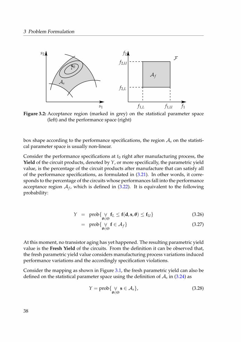
3 Problem Formulation
f1,L
s2
s1
f2
f1,U f1
f2,U
f2,L
A f
F
As
s0
Figure 3.2: Acceptance region (marked in grey) on the statistical parameter space(left) and the performance space (right)
box shape according to the performance specifications, the region As on the statisti-cal parameter space is usually non-linear.
Consider the performance specifications at t0 right after manufacturing process, theYield of the circuit products, denoted by Y, or more specifically, the parametric yieldvalue, is the percentage of the circuit products after manufacture that can satisfy allof the performance specifications, as formulated in (3.21). In other words, it corre-sponds to the percentage of the circuits whose performances fall into the performanceacceptance region A f , which is defined in (3.22). It is equivalent to the followingprobability:
Y = prob{ ∀θ∈Θ
fL ≤ f(d, s, θ) ≤ fU} (3.26)
= prob{ ∀θ∈Θ
f ∈ A f } (3.27)
At this moment, no transistor aging has yet happened. The resulting parametric yieldvalue is the Fresh Yield of the circuits. From the definition it can be observed that,the fresh parametric yield value considers manufacturing process variations inducedperformance variations and the accordingly specification violations.
Consider the mapping as shown in Figure 3.1, the fresh parametric yield can also bedefined on the statistical parameter space using the definition of As in (3.24) as
Y = prob{ ∀θ∈Θ
s ∈ As}, (3.28)
38

3.4 Fresh Yield and Aged Yield
which is equivalent of the integration of pdf of s in As:
Y =∫· · ·
∫s∈As
pdf(s)ds (3.29)
An important observation from Figure 3.2 concerning the yield definition is that, theregion As on the statistical parameter space cannot be calculated explicitly from per-formance specifications as shown in (3.24). In other words, whether or not a circuitstatistical parameter vector lies inside the region As can only be checked on the per-formance space by means of circuit simulations.
When the transistor aging effects are taken into consideration, circuit performancesdegrade over time, as introduced in (3.20), but both of the performance acceptanceregion A f and statistical parameter acceptance region As do not change over time,since the performance specifications are fixed boundary requirements.
Thus the performance acceptance region A f at age t is
A f = {f(t) | fi(t) ≤ fi,U ∧ fi,L ≤ fi(t), i = 1, . . . , nf} (3.30)= {f(t) |fL ≤ f(t) ≤ fU} (3.31)
and statistical parameter acceptance region As at age t is
As = {s(t)| ∀θ∈Θ
fL ≤ f(d, s(t), θ) ≤ fU} (3.32)
= {s(t)| ∀θ∈Θ
f(d, s(t), θ) ∈ A f } (3.33)
Figure 3.3 shows the acceptance region (marked in grey) on the statistical parameterspace and the performance space, with consideration of transistor aging. On the sta-tistical parameter space, the two groups of ellipsoids correspond to the level contoursof the pdf of the Gaussian distributed two-dimensional statistical parameter before(at t0) and after (at t1) transistor aging.
Considering transistor aging on top of the manufacturing process variations, theAged Yield Y(t) at t corresponds to the percentage of the circuits which still cansatisfy all of the performance specifications. Using (3.14), (3.15) and (3.20), Y(t) canbe formulated accordingly as
Y(t) = prob{ ∀θ∈Θ
f(t) ∈ A f } (3.34)
= prob{ ∀θ∈Θ
s(t) ∈ As} (3.35)
=∫· · ·
∫s(t)∈As
pdf(s(t))ds(t) (3.36)
39

3 Problem Formulation
f1,L
s2
s1
f2
f1,U f1
f2,U
f2,L
A f
F
As
agings0(t0)
s0(t1)
Figure 3.3: Acceptance region (marked in grey) on the statistical parameter space(left) and the performance space (right) with transistor aging
As can be seen in Figure 3.3, since the original distribution around s0(t0) will shiftto a new distribution with new mean vector s0(t1) and covariance matrix C(t1), acertain percentage of the fresh circuits which satisfies the specification at t0 will fallout of the acceptance region at t1, causing an aged yield loss.
It is important to note that, at t1, after parameter aging happens, the mean vector ofthe aged statistical parameter, s0(t1), may still satisfy all of the performance specifi-cations. But it cannot ensure that the whole distributions of the statistical parameterat t1 remain inside the statistical parameter acceptance region As at t1. The problemmay get even worse if the spread of the aging process itself is taken into account.In that case, the distribution of certain statistical parameters may spread even morewidely than that of the fresh circuit, resulting in more serious loss of the aged yieldvalue.
3.4.2 Statistical Analysis Method
As mentioned in the last section, the non-linear feature of the acceptance region Ason the statistical parameter space makes the calculation of the yield according to theintegration as in (3.29) a difficult task.
For integrated circuit designers, the traditional method of the circuit yield estimationis the statistical analysis using Monte-Carlo simulations. The information regardingprocess variations are provided by the manufacturer in terms of statistical distribu-tions of certain modelcard parameter values. In this case, those values of modelcardparameters are the results of the calculation of certain statistical parameters, in steadof a fixed value as in nominal cases.
40

3.4 Fresh Yield and Aged Yield
Then, Monte-Carlo method calculates the circuit parametric yield value by randomsampling inside the statistical parameter space according to the provided distribu-tional information. The performance value corresponding to each sample is checkedover the predefined performance specifications. Since the output of each sample iseither 1 (pass) or 0 (fail), such an experiment is actually a Bernoulli Trial [GS97].
If the real theoretical yield is denoted by Y, the experimental yield is denoted by Y,the total number of samples is denoted by N, then Y is obtained by
Y =ΣN
i=1Xi
N(3.37)
where Xi is either 1 or 0, corresponding to the output of each Bernoulli Trial sample.
According to the law of large numbers [GS97], Y and Y follows:
P(|Y−Y| ≥ ε)→ 0, when N → ∞ (3.38)
where ε is any positive real numbers. (3.38) indicates that, theoretically only whenthe sample size N approaches infinity then the approximated yield Y is equal to thetheoretical yield Y. This is the condition that of course is not applicable in practice.
In practice, the reliability of such estimation is determined through a confidence levelCL, as well as confidence intervals ±ε. As introduced in [DS98], [Li10], [Pha06],[Gra07], according to Chebyshev inequality, Y and Y follows:
P(|Y−Y| ≥ ε) ≤σ2
Yε2 (3.39)
where σ2Y is the variance of Y. From probability theory Y has expectation Y and
variance Y(1−Y)/N. If we define a confidence level
CL = prob{|Y− Y| < ε}, (3.40)
then from (3.39), CL can be derived as
CL ≥ 1− Y · (1−Y)Nε2 (3.41)
To meet a certain confidence level CL, the number of samples N must satisfy
N ≤ Y · (1−Y)(1− CL)ε2 (3.42)
41

3 Problem Formulation
The confidence interval±ε for a given sample size N and confidence level CL satisfies
ε ≤
√Y · (1−Y)
N · (1− CL)(3.43)
The confidence level CL tells how often the theoretical yield Y lies within the confi-dence interval ±ε of the estimated yield Y. For example, for a typical value of CLof 95% and with ε equals 5%, we can be sure that, with a probability of 95%, thetheoretical yield Y lies within the region [Y− 0.05, Y + 0.05].
The relationship among the sample size N, the confidence level CL, as well as the con-fidence interval ±ε is clear from (3.41)-(3.43). For a given CL, a narrower confidenceinterval requires a larger sample size N to ensure. For a given confidence interval, toreach a higher confidence level, a larger N is also needed. Last but not least, since theproduct Y · (1− Y) has a maximal value at Y = 0.5, the confidence interval is also afunction of the value of Y. Around 50% yield, the confidence interval itself becomeswider, indicating that a larger N is needed in order to achieve the same CL for otheryield values.
Due to the requirements on the sample size N discussed above, for complicatedcircuits the Monte-Carlo method is limited by its simulation costs. The alternativemethod for parametric yield evaluation will be presented in detail in Chapter 4.
The determination of the aged yield value Y(t) can also be carried out by Monte-Carlo simulations on the aged circuits. In this case, the aged transistor modelcardwith aged model parameters as well as variation information are needed. UsingMonte-Carlo simulation, the approximated aged parametric yield value Y(t) at t isgiven by
Y(t) =ΣN
i=1X(t)i
N(t)(3.44)
where where X(t)i is either 1 or 0, corresponding to the output of each Bernoulli Trialsample at t, and N(t) corresponds to the satisfied samples and total sample size at trespectively.
To avoid the simulation overhead as introduced above, the formulation of the agedyield analysis based on geometric approximation of the aged robustness measureswill be presented later in Chapter 4.
One advantage of the statistical analysis method like Monte-Carlo simulation is that,the analysis accuracy depends neither on the number of parameters of the circuit,nor the linearity of the performances. This makes Monte-Carlo simulation applicableto a variety of circuits with easy setup and accurate estimation results, provided thesample size is large enough.
42

3.5 Sizing Rules with Aging
3.5 Sizing Rules with Aging
As shown in [SEGA99], [GZEA01], [MGS08], [Mas10], sizing rules of the analog cir-cuits are constraints that must be satisfied during circuit sizing. They include, forexample, geometry constraints (e.g., transistor width, length, area) and electrical con-straints (e.g., transistor gate-source voltage vgs, drain-source voltage vds). They areused to ensure the proper function of the circuits, for example, preventing the transis-tors from entering inappropriate operation regions, or limiting the voltage differenceof vds in a transistor pair to a certain value, etc.
Figure 3.4 shows a most simple current mirror made up a pair of NMOS transistors.Table 3.1 below lists a complete set of sizing rules for this current mirror.
vgs1
M2M1
id1
vds1 vds2
id2
vgs2
Figure 3.4: Example: a simple current mirror
Table 3.1: Example: sizing rules for a simple current mirror.Geometrical Electrical
Func
tion
L2 = L1 (3.45)W2 = K ·W1 (3.46)
vgs1,2 −Vth ≥ 0 (3.47)
vds1,2 ≥ 0 (3.48)
vds1,2 − (vgs1,2 −Vth1,2) ≥ Vsatmin (3.49)
|vds2 − vds1 | ≤ ∆Vdsmax (3.50)
Rob
ustn
ess
W1 ≥Wmin (3.51)L1 ≥ Lmin (3.52)
W1 · L1 ≥ Amin (3.53)
vgs1,2 −Vth1,2 ≥ Vgsmin (3.54)
As can be seen from Table 3.1, the sizing rules can be classified into several categories:
43

3 Problem Formulation
• Geometrical and Electrical:Geometrical sizing rules refer to constraints of transistor geometries, such aswidth, length, area. They are the requirements concerning the relationship ofgeometrical parameters between a pair or a group of transistors, for example,transistors making up of a differential stage, a current mirror, or a level shifter.Electrical sizing rules refer to the constraints of voltages and currents betweentransistor nodes, such as gate-to-source voltage vgs, drain-to-source current ids,etc.
• Function and Robustness:A less obvious category in contrast to the above is based on the difference be-tween circuit Function and Robustness. Sizing rules concerning function are thecritical requirements to ensure the defined function of the transistor and transis-tor blocks. For example, vgs must be greater than the threshold voltage in orderto operate the single transistor (3.47), the saturation condition (3.49) must be metfor the transistors in a current mirror to ensure the function of that current mir-ror. Robustness sizing rules, on the other hand, give the additional requirementsfor circuit’s proper working under variations of operating conditions and processmanufacturing parameters. Take again the example of vgs. For robustness it mustbe greater than the threshold voltage at least the amount of Vgsmin (3.54).
• Equality and Inequality:The difference between equality and inequality sizing rules comes from the con-straint formulation itself. The equality sizing rules appear for transistor geome-tries. They ensure the dependency of design parameters d among different tran-sistors, through the relationship of equality, which can be summarized as
c(d) = 0 (3.55)
Each equality sizing rules reduces the dimension of the design parameter spaceD in (3.2) by one, since in this case one design parameter is just the duplicate ofthe other. Such design space shrink can speed up the sizing process. Inequal-ity sizing rules concern the relationship between either electrical or geometricalparameters. For example, the saturation conditions for transistors, or the mini-mum values for transistor width or length. These inequality constraints furtherlimit the available range for each design parameter. Without loss of generality,the inequality sizing rules can be summarized as
c(d) ≥ 0 (3.56)
The resulting space of design parameter is now limited to feasible design parameterspace D′:
D′ = {d ∈ D|c(d) ≥ 0} (3.57)
44

3.6 Summary
which is the part of design parameter space D in (3.2) where all inequality sizingrules are satisfied. The corresponding performance space F from (3.19) becomesthe feasible performance space F ′:
F ′ = {f|f evaluated at (d, s, θ) ∧ c(d) ≥ 0} (3.58)
As pointed out in [Mas09], a feasible circuit design does not necessarily meet all per-formance specifications. The feasible performance space F ′ is not the same as theperformance acceptance region A f in (3.22). Considering both feasibility and perfor-mance specification, the feasible acceptance region A f ’ can be defined as
A′f = A f ∩ F ′ = {f|f evaluated at (d, s, θ) ∧ fL ≤ f ≤ fU ∧ c(d) ≥ 0} (3.59)
When transistor parameters degrade over operating time, some electrical sizing rulesare influenced. As can be observed from Table 3.1, for example, the electrical sizingrules involving the value of transistor threshold voltage, such as (3.47), (3.49), willchange their left-hand-side values over time, due to the drift of Vth. These aging-sensitive constraints might be violated during lifetime operation, or even if they arestill fulfilled, their distances to the boundary values might decrease, i.e., they mightmore likely be violated after aging in comparison to the fresh circuit.
As a result, the feasible design parameter space D′ changes over time. At age t theaged feasible design parameter space can be denoted as D′(t). In the proposed relia-bility optimization methodology, both fresh and aged sizing rules must be consideredand checked.
3.6 Summary
This chapter formulates the basic problem of fresh and aged yield analysis consider-ing process variations and transistor aging. Different types of circuit parameters andperformances are defined for future discussion. The statistical analysis method ofthe fresh and the aged yield values is introduced. The requirements to meet certainconfidence level on the sample size of the statistical yield analysis are formulated indetail. As can be seen, a large number of random samples are needed for the sta-tistical analysis method. Though accurate and easy to perform by circuit designers,the statistical yield analysis method needs a huge simulation costs. Further more, therelationship concerning circuit age and lifetime is discussed. The circuit robustnessand the total area spent in layout can be two major concern for future circuit designfor reliability.
45


Chapter 4
Aged Yield Optimization with Freshand Aged Sizing Rules
This chapter proposes the complete sizing flow towards aged yield optimization withfresh and aged sizing rules checking. As already discussed in section 3.4.2, the analy-sis of fresh and aged yield of the circuit using statistical method is limited by its highsimulation costs. Instead, the methodology presented in this chapter is based on theapproximation of the acceptance region using so-called worst-case distance.
4.1 Worst-Case Distance
The worst-case distance of a circuit is used to model the circuit robustness and the re-sulting yield value, considering the manufacturing process variations and variousoperating conditions. The idea of the worst-case distance was first proposed byAntreich et al. in [AGW94]. Its complete descriptions and applications in state-of-the-art design centering methodologies can be found in [Sch03] and [Gra07].
In this section, the idea of the worst-case distance is briefly introduced. It is refinedlater in the next section into the aged worst-case distance and the corresponding agedyield approximation considering transistor parameter aging.
4.1.1 Yield Analysis and Worst-Case Analysis
At first, two different types of tasks relating with process variations and various op-erating conditions are explained.
47

4 Aged Yield Optimization with Fresh and Aged Sizing Rules
Worst−Case Analysis
Yield Analysis
fi,L/ fi,U
Performance SpecificationsYield Partitions Yi,L/Yi,U
Yield Y
Figure 4.1: The relationship between yield analysis and worst-case analysis.
• The task of yield analysis is to compute the parametric yield value (3.26) giventhe performance specification (3.21) as input. It computes how many percentsof the products can satisfy the given performance specification, i.e., what is theparametric yield value considering manufacturing process variations and variousoperating conditions.
• The task of worst-case analysis, on the other hand, is to compute the performancespecification that must be accepted, in order to achieve a given parametric yieldvalue. It is the inverse of the yield analysis task. In the worst-case analysis, the de-sign robustness requirements considering manufacturing process variations andvarious operating conditions, i.e., the parametric yield, are given as input, and thegoal is to obtain the worst performance boundary values that have to be acceptedto achieve such requirements.
As can be seen, the tasks of yield analysis and worst-case analysis manifest them-selves by switching their respective inputs and outputs. Such relationship betweenthe task of yield analysis and worst-case analysis is shown in Figure 4.1. In the con-text of this thesis, the task of yield analysis is of interest. In this case, the circuitsperformance specifications (3.21) in the performance space F (3.19) are given as fixedvalues, and the goal is to find the corresponding parametric yield values, i.e., the up-per half mapping of the Figure 4.1. This mapping will be refined later as we discussabout the worst-case parameters and worst-case distances.
As shown in Figure 3.2 and defined in (3.26) and (3.28), the parametric yield can becomputed by two approaches, either in the performance space F or in the statisticalparameter space.
The advantage of the first approach is that the performance specifications (3.21) in theperformance space F are explicitly known. The evaluation of the parametric yield
48
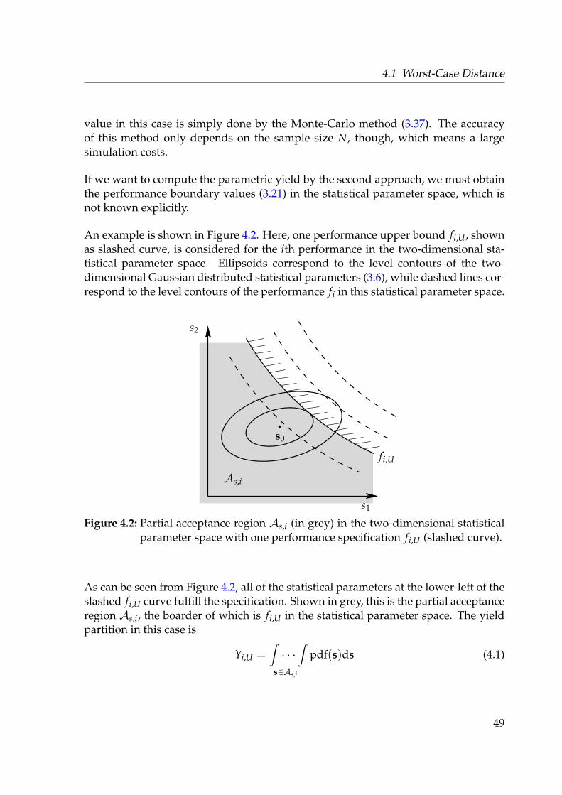
4.1 Worst-Case Distance
value in this case is simply done by the Monte-Carlo method (3.37). The accuracyof this method only depends on the sample size N, though, which means a largesimulation costs.
If we want to compute the parametric yield by the second approach, we must obtainthe performance boundary values (3.21) in the statistical parameter space, which isnot known explicitly.
An example is shown in Figure 4.2. Here, one performance upper bound fi,U, shownas slashed curve, is considered for the ith performance in the two-dimensional sta-tistical parameter space. Ellipsoids correspond to the level contours of the two-dimensional Gaussian distributed statistical parameters (3.6), while dashed lines cor-respond to the level contours of the performance fi in this statistical parameter space.
s0
s1
s2
As,i
fi,U
Figure 4.2: Partial acceptance region As,i (in grey) in the two-dimensional statisticalparameter space with one performance specification fi,U (slashed curve).
As can be seen from Figure 4.2, all of the statistical parameters at the lower-left of theslashed fi,U curve fulfill the specification. Shown in grey, this is the partial acceptanceregion As,i, the boarder of which is fi,U in the statistical parameter space. The yieldpartition in this case is
Yi,U =∫· · ·
∫s∈As,i
pdf(s)ds (4.1)
49

4 Aged Yield Optimization with Fresh and Aged Sizing Rules
4.1.2 Yield Estimation Based on Worst-Case Distance
Now the yield partition Yi,U in Figure 4.2 will be approximated using worst-casedistance.
First, notice in Figure 4.2 that there exists a certain ellipsoid, which is one of thelevel contours of the Gaussian distributed statistical parameters, that just touches theperformance boundary fi,U at one point. We call this point the worst-case parametersi,w, see Figure 4.3. It has such a property that, among all of the parameter pointsalong the performance boundary fi,U in the statistical parameter space, si,w has thehighest possibility of occurrence. Remember each ellipsoid of the level contours ofthe Gaussian distributed statistical parameters corresponds to the same probabilityof occurrence, and the smaller the ellipsoid is, the bigger probability of occurrence itcorresponds to.
For the Gaussian distributed statistical parameter s, the level contour correspondingto si,w can be formulated from (3.7) as
β2i,w = (si,w − s0)
T ·C−1 · (si,w − s0) (4.2)
and βi,w is called worst-case distance between the mean value and the boundary of theith performance feature fi.
Second, the performance boundary fi,U in the statistical parameter space is linearizedat the worst-case parameter point si,w. The linearization error in this case is mini-mum, since the linear approximation is accurate enough at the point with highestprobability of occurrence. The linearized performance model in the statistical pa-rameter space from si,w is
f i = f (si,w) +∇s f (s)|s=si,w · (s− si,w) (4.3)= fi,U +∇s f (s)|s=si,w · (s− si,w), (4.4)
where Nabla operator ∇s is defined as
∇s =
[∂
∂s1,
∂
∂s2, · · · ,
∂
∂sns
]T(4.5)
and for the linear performance model at the worst-case point, its sensitivity overstatistical parameter s is a constant, which is denoted as gi:
∇s f (s)|s=si,w ≡ gTi = const. (4.6)
as can be seen in Figure 4.3.
50

4.1 Worst-Case Distance
s0
s1
s2
As,i
si,w
f i = fi,U
f i < fi,U
βi,w
gi ≡ ∇ f (si,w)
Figure 4.3: The idea of the worst-case distance βw. As is the linear bounded approxi-mated acceptance region.
With the linear performance model at the worst-case point, the partial acceptanceregion As,i now can be approximated by this linear bounded single-side acceptanceregion As,i:
As,i = {s|gTi · (s− si,w) ≤ 0} (4.7)
= {s| f i ≤ fi,U} (4.8)
which corresponds to the grey area in Figure 4.3. Note that the gap between thisgrey area As,i and the original performance boundary curve is the error from thislinear approximation. Since the linear performance model is accurate at the worst-case point si,w, the linear approximation error is thus kept minimum.
Based on the approximated acceptance region As,i, (4.1) becomes
Yi,U ≈∫· · ·
∫s∈As,i
pdf(s)ds (4.9)
Now we formulate (4.9) in the performance space and relate it with worst-case dis-tance. With Gaussian distributed statistical parameters s ∼ N (s0, C) and (4.3), thelinear performance model f i in (4.3) can be transformed into Gaussian distributedperformance as
f i ∼ N ( f i,0, σ2f i), (4.10)
51

4 Aged Yield Optimization with Fresh and Aged Sizing Rules
where
f i,0 = fi,U + gT · (s0 − si,w) (4.11)
σ2f i
= gT ·C · g (4.12)
The pdf of the Gaussian distributed f i thus is
pdf f i( f i) =
1√2π · σf i
· e− 1
2
(f i− f i,0
σf i
)2
(4.13)
So (4.9) in the performance space is
Yi,U ≈∫ fi,U
−∞pdf f i
( f i)d f i (4.14)
By inserting (4.13) into (4.14), we have
Yi,U ≈∫ fi,U− f i,0
σf i
−∞
1√2π· e− 1
2 ξ2dξ (4.15)
The upper limit of the integration (4.15) is equivalent to βi,w. This can beshortly proved as follows. A complete discussion of βi,w concerning performancelower/upper bounds and whether or not the mean value of the statistical parameterfalls into the statistical acceptance region will be presented in the next section.
From (4.11) and (4.12), we have
fi,U − f i,0
σf i
= −gT · (s0 − si,w)√gT ·C · g
(4.16)
Since the level contour β2i,w (4.2) touches the performance boundary at si,w, its orthog-
onal is parallel to g:C−1 · (si,w − s0) = λ · g (4.17)
The following equation can be obtained
(si,w − s0) =βi,w ·C · g√
gT ·C · g(4.18)
52

4.1 Worst-Case Distance
so that the right side of (4.16) is equal to βi,w, and we have
fi,U − f i,0
σf i
= βi,w (4.19)
Yi,U can now be expressed using worst-case distance as
Yi,U ≈∫ βi,w
−∞
1√2π· e− 1
2 ξ2dξ (4.20)
From (4.20) the yield value can be obtained immediately for different worst-case dis-tance βw values. The correspondence between them is shown in Figure 4.4 and Table4.1 below.
Figure 4.4: Yield values over different worst-case distances.
Table 4.1: Worst-case distances and the corresponding yield value.
βw -4 -3 -2 -1 0 1 2 3 4
Yield [%] 0.01 0.13 2.28 15.87 50.00 84.13 97.73 99.87 99.99
The meaning of the worst-case distance can be interpreted by (4.19). For a perfor-mance feature, βw is the distance between the mean value and the worst-case valueof that performance. It is measured in the unit "performance standard deviation σ".βw = 3 means the worst-case performance value is three times of performance stan-dard deviation away from the mean value of that performance, and it is commonlyunderstood as "βw-sigma" design.
As can be seen from (4.20) and Table 4.1, the bigger the value of βw is, the higherthe value of yield it corresponds to. One advantage of using worst-case distance as
53
4 Aged Yield Optimization with Fresh and Aged Sizing Rules
a measurement of the circuit robustness is that, when the yield value approaches 0%or 100%, the tiny difference between yield value almost disappear, as can be seen inFigure 4.4, whereas the worst-case distance values can still discriminate themselvesin such situations. For example, when the worst-case distance equals four, it corre-sponds to a yield value of 99.99968%, and when the worst-case distance equals five,it represents a yield of 99.99999%. This advantage is very important in the algorithmdesign for yield optimization/design centering.
Another observation from the above discussion is that, the worst-case distance βwwill be negative, if the mean value of the performance violates the specification. Adetailed formulation concerning the negative worst-case distance will be presentedlater in the next section. Last but not least, for different performance standard de-viations, a same distance between the mean value and the worst-case value of theperformance corresponds to different worst-case distances and thus different yields.
The overall yield of the circuit can be estimated by a Monte-Carlo analysis on thepiecewise linear acceptance region of all performance specifications with no addi-tional simulation cost. The total yield Y is bounded by:
1−∑i(1−Yi) . Y . min
iYi (4.21)
Since a smaller worst-case distance during transistor aging leads to more signifi-cant yield loss, it is important in the new design flow to analyze and optimize theworst-case distances and the corresponding yield values for the fresh circuit. Thosereliability-sensitive worst-case distances should be increased in order to be more ro-bust over transistor aging.
4.1.3 Problem Formulation towards Worst-Case Distance BasedYield Estimation
In practice, neither the worst-case parameter si,w nor the worst-case distance isknown a priori. Thus formulations towards mathematical optimization solutions areneeded. The basic idea can be derived from the above discussion, i.e., the worst-caseparameter si,w has the highest probability of occurrence among all statistical param-eters on the performance specification border [Gra07].
For one of the performance fi, whose mean value satisfies the specification fi ≤ fi,U,to locate the worst-case parameter si,w is equivalent to find the statistical parametervector with highest probability of occurrence among all parameters which are outsideor on the boarder of the acceptance region As,U,i:
54

4.1 Worst-Case Distance
fi ≤ fi,U and s0 ∈ As,U,i:
maxs
pdfN(s), s.t. s 6∈ As,U,i (4.22)
To further extend the formulation in (4.22), we first consider the variations of op-erating parameters such as operating temperature and supply voltage of the cir-cuit [GWA93]. A statistical parameter vector s is within the partial acceptance re-gion, s ∈ As,U,i, for a specification fi ≤ fi,U means that, the maximal performancevalue over operating parameter variations still satisfies that specification, and viceversa, i.e., once the maximal performance value over operating parameter variationsviolates the specification fi ≤ fi,U, then it can be concluded that s 6∈ As,U,i:
fi ≤ fi,U:
s ∈ As,U,i ⇔ maxθ∈Θ
fi(s, θ) ≤ fi,U (4.23)
s 6∈ As,U,i ⇔ maxθ∈Θ
fi(s, θ) > fi,U (4.24)
Another development from (4.22) is that, to maximize the probability density func-tion is equivalent to minimize β, i.e., minimize the size of the equidensity contouraccording to (3.7).
Thus, considering nf performance specifications, (4.22) can be reformulated as
mins
β2i (s), s.t. max
θ∈Θfi(s, θ) ≥ fi,U, i = 1, . . . , nf. (4.25)
The other cases corresponding to the specification fi ≥ fi,L and whether or not themean value satisfies the specification can be formulated accordingly as:
fi ≤ fi,U and s0 6∈ As,U:
mins
β2i (s), s.t. max
θ∈Θfi(s, θ) ≤ fi,U, i = 1, . . . , nf. (4.26)
fi ≥ fi,L and s0 ∈ As,L:
mins
β2i (s), s.t. min
θ∈Θfi(s, θ) ≤ fi,L, i = 1, . . . , nf. (4.27)
fi ≥ fi,L and s0 6∈ As,L:
mins
β2i (s), s.t. min
θ∈Θfi(s, θ) ≥ fi,L, i = 1, . . . , nf. (4.28)
The solutions of (4.25)-(4.28) give the worst-case distance βi,w for each performancespecification, and can be used in the yield approximation as introduced in Section4.1.2.
55

4 Aged Yield Optimization with Fresh and Aged Sizing Rules
4.1.4 Solution using Lagrangian Functions
In the following, the analytical form of the worst-case distance βw is developed usingLagrangian function with its first-order optimality condition [Gra07]. Such formu-lation is needed in the discussion about the gradient of the worst-case distance lateron. The performance index i is left out for simplicity in the discussion below.
Inside (4.25) and (4.26), the evaluation of the constraint requires the solving of thefollowing maximization problem first:
maxθ
f (θ), s.t. θL ≤ θ ≤ θU (4.29)
The Lagrangian function of (4.29) can be written as
LU(θ, λL, λU) = − f (θ)− λTL · (θ− θL)− λT
U · (θU − θ) (4.30)
Similarly, for the inner optimization problems of (4.27) and (4.28), the Lagrangianfunction can be written as
LL(θ, λL, λU) = f (θ)− λTL · (θ− θL)− λT
U · (θU − θ) (4.31)
By applying (4.30) and (4.31), the Lagrangian functions of (4.25)-(4.28) can be writtenas:
f ≤ fU and s0 ∈ As,U:
L(s, θ, λ, λL, λU) = β2(s) + λ · ( fU + LU(θ, λL, λU)) (4.32)
f ≤ fU and s0 6∈ As,U:
L(s, θ, λ, λL, λU) = β2(s)− λ · ( fU + LU(θ, λL, λU)) (4.33)
f ≥ fL and s0 ∈ As,L:
L(s, θ, λ, λL, λU) = β2(s)− λ · ( fL −LL(θ, λL, λU)) (4.34)
f ≥ fL and s0 6∈ As,L:
L(s, θ, λ, λL, λU) = β2(s) + λ · ( fL −LL(θ, λL, λU)) (4.35)
Applying Karush-Kuhn-Tucker conditions [Fle87], [NW00] for one of the above La-grangian functions (4.32), and with (4.2), the solution sw,U can be obtained:
56
4.1 Worst-Case Distance
f ≤ fU and s0 ∈ As,U:
∇L(sw,U) = 2C−1 · (sw,U − s0) + λw,U · ∇LU(sw,U) ≡ 0 (4.36)
where
∇LU(sw,U) = −∇ f (sw,U) (4.37)
from the Lagrangian function (4.30).
The formulation of (4.36) an (4.37) can lead to the representation of the worst-caseparameter in the case f ≤ fU and s0 ∈ As,U:
(sw,U − s0) =λw,U
2·C · ∇ f (sw,U) (4.38)
The worst-case distance in (4.2) can then be represented as
β2w,U =
λ2w,U
4· ∇ f (sw,U)
T ·C · ∇ f (sw,U) (4.39)
which givesλw,U
2=
βw,U√∇ f (sw,U)T ·C · ∇ f (sw,U)
(4.40)
The worst-case parameter can be represented by applying (4.40) into (4.38):
(sw,U − s0) =βw,U√
∇ f (sw,U)T ·C · ∇ f (sw,U)·C · ∇ f (sw,U) (4.41)
For the cases f ≤ fU and s0 6∈ As,U, the worst-case parameter is
(sw,U − s0) = −βw,U√
∇ f (sw,U)T ·C · ∇ f (sw,U)·C · ∇ f (sw,U) (4.42)
The other two cases corresponding to (4.34) and (4.35) can be derived in a similarway:
f ≥ fL and s0 ∈ As,L:
(sw,L − s0) = −βw,L√
∇ f (sw,L)T ·C · ∇ f (sw,L)·C · ∇ f (sw,L) (4.43)
57

4 Aged Yield Optimization with Fresh and Aged Sizing Rules
f ≥ fL and s0 6∈ As,L:
(sw,L − s0) =βw,L√
∇ f (sw,L)T ·C · ∇ f (sw,L)·C · ∇ f (sw,L) (4.44)
To obtain an analytical expression for the worst-case distance βw,L/U, a linear per-formance model can be built up at the worst-case parameter vector sw,L/U in thestatistical parameter space as:
f w(s) = fL/U +∇ f (sw,L/U)T · (s− sw,L/U) (4.45)
At the nominal parameter vector s0, (4.45) gives
∇ f (sw,L/U)T · (sw,L/U − s0) = fL/U − f w(s0) (4.46)
Inserting (4.42) and (4.43) into (4.46) gives:
For the cases f ≤ fU and s0 6∈ As,U, as well as f ≥ fL and s0 ∈ As,L:
βw,L/U =f w(s0)− fL/U√
∇ f (sw,L/U)T ·C · ∇ f (sw,L/U)(4.47)
=∇ f (sw,L/U)
T · (s0 − sw,L/U)
σf w
(4.48)
Inserting (4.41) and (4.44) into (4.46) gives:
For the cases f ≤ fU and s0 ∈ As,U, as well as f ≥ fL and s0 6∈ As,L:
βw,L/U =fL/U − f w(s0)√
∇ f (sw,L/U)T ·C · ∇ f (sw,L/U)(4.49)
=∇ f (sw,L/U)
T · (sw,L/U − s0)
σf w
(4.50)
It is clear from (4.47)-(4.50) that, if the mean value of the statistical parameter andperformance violates the specification, the worst-case distance is negative.
58

4.2 Aged Worse-Case Distance and Aged Yield
4.2 Aged Worse-Case Distance and Aged Yield
When transistor parameters degrade over time, the statistical parameters shift theirdistributions in the statistical parameter space as introduced in Figure 3.3. Using thesimilar modeling method as introduced above, the worst-case distance during tran-sistor aging with respect to one performance specification can be illustrated in Figure4.5. For simplicity, the performance index i is left out in the discussion hereafter.
s2
s0(t1)
s0(t0)
βw(t0)
βw(t1)
s1
As(t0)
As(t1)
aging
g(t0)
fU
sw(t0)
sw(t1)
g(t1)
Figure 4.5: The degradation of worst-case distance from t0 to t1 with respect to oneperformance specification fU (slashed curve).
In Figure 4.5, again, one performance upper bound fU, shown as slashed curve, isconsidered in the two-dimensional statistical parameter space. The two groups ofellipsoids correspond to the level contours of the two-dimensional Gaussian dis-tributed statistical parameters at t0 and t1 respectively. During parameter agingfrom t0 to t1, both of the mean and the worst-case value of the statistical parame-ters change, as shown in Figure 4.5.
To approximate the aged yield using aged worst-case distance value, a linear perfor-mance model is built up at t0 and t1 respectively, from the corresponding worst-casepoint sw(t0) and sw(t1). The sensitivity of the linear performance model over statis-tical parameters is g(t0) and g(t1) respectively. The linear bounded approximatedacceptance region is now As(t0) and As(t1). Note the linear approximation error at
59
4 Aged Yield Optimization with Fresh and Aged Sizing Rules
the different points on the performance boundary in this case, which lead to the slightdifference in the two approximated acceptance regions.
At time t1, the linearized performance model from sw(t1) is
f (t1) = fU + gT(t1) · (s(t1)− sw(t1)) , (4.51)
and the corresponding linear bounded approximated acceptance region at t1 is
As(t1) = {s(t1)|gT(t1) · (s(t1)− sw(t1)) ≤ 0} (4.52)= {s(t1)| f (t1) ≤ fU} (4.53)
With Gaussian distributed statistical parameters at t1: s(t1) ∼ N (s0(t1), C(t1)), thelevel contour corresponding to sw(t1) is
β2w(t1) = (sw(t1)− s0(t1))
T ·C−1(t1) · (sw(t1)− s0(t1)), (4.54)
and the linear performance model can be transformed into Gaussian distributed per-formance as
f (t1) ∼ N ( f 0(t1), σ2f (t1)), (4.55)
where
f 0(t1) = fU + gT(t1) · (s0(t1)− sw(t1)) (4.56)
σ2f (t1) = gT(t1) ·C(t1) · g(t1) (4.57)
The aged yield value at t1 can be approximated as
YU(t1) ≈∫ fU− f 0(t1)
σf (t1)
−∞
1√2π· e− 1
2 ξ2dξ, (4.58)
where the upper limit of the integration (4.58) can be reformulated, similar to (4.16)-(4.19), using (4.56), (4.57) and (4.54) as
fU − f 0(t1)
σf (t1)= −gT(t1) · (s0(t1)− sw(t1))√
gT(t1) ·C(t1) · g(t1)(4.59)
= βw(t1) (4.60)
The aged yield at t1, YU(t1), can be expressed using aged worst-case distance as
YU(t1) ≈∫ βw(t1)
−∞
1√2π· e− 1
2 ξ2dξ (4.61)
A complete formulation of the aged worst-case distance concerning performancelower/upper bounds and whether or not the mean value of the aged statistical pa-rameter falls into the statistical acceptance region is shown in Section 4.3.5.
60

4.3 Design Flow
4.3 Design Flow
As transistor parameters degrade over time, the aged worst-case distance values de-crease, resulting in an increasing yield loss over time. In the proposed yield analysisand optimization flow, the fresh circuit is analyzed and optimized for x-sigma robust-ness, both fresh and aged sizing rules as well as the maximum layout area constraintare checked. For those aging-sensitive performances, the corresponding worst-casedistances will be increased for the fresh circuit, ensuring a more robust design overprocess variations and transistor aging.
One assumption of the proposed fresh circuit optimization flow is that, for analogcircuits, annealing from NBTI is a minor effect due to the constant existence of dc bi-asing voltages [JRSR05]. Thus the aged yield decreases over time with the monotonicaging of βi,w(t). The robustness of the circuits during the lifetime can be ensured byoptimizing fresh circuits with enough design margins.
The core part of the proposed reliability optimization flow is shown in Figure 4.6.The input of the flow is the fresh circuit netlist with initial design parameters. Then,the step of the fresh circuit optimization with one maximum area constraint Amax isperformed. This step involves the checking of sizing rules for both fresh and agedcircuits. The output of this step is the optimal design parameters for the circuit. Then,the aged yield can be analyzed, provided that the aged circuit netlist is obtained. Theaged circuit netlist is obtained using AgeMOS model from RelXpert as explainedlater.
Running the flow repeatedly with increasing maximum area value Amax as a con-straint, the designer can obtain the trade-off between approximated layout area andcircuit reliability, and choose a reasonable area with its acceptable aged yield value.
In the following, Section 4.3.1 gives in detail the simulation flow of the aged circuitand how the aged performances are obtained. Section 4.3.2 explains the checkingof fresh and aged sizing rules. Section 4.3.3 discusses the approximation of the cir-cuit layout area. Section 4.3.4 and Section 4.3.5 detail the problem formulations asa numerical optimization problem for the fresh circuit optimization and aged yieldanalysis.
4.3.1 Simulation Flow of the Aged Circuit
This Section briefly introduces the workflow concerning the generation and simula-tion of the aged circuit.
61

4 Aged Yield Optimization with Fresh and Aged Sizing Rules
Maximum Area Constraint
Aged Netlist
Fresh Netlist withInitial Design Parameters
Fresh Netlist with
Aged Yield Analysis
Optimal Design Parameters
Fresh Circuit
Aged Circuit
Sizing Rules Checking for
Sizing Rules Checking for
Fresh Circuit Optimization with
AgeMOS Model
AgeMOS Model
Figure 4.6: Core of the proposed reliability optimization flow with one maximumarea constraint.
The complete workflow is shown in Figure 4.7. The round-corner boxes indicate theinput and the output of the flow. The tool RelXpert from Cadence [cad] is used fortransistor aging calculation and aged circuit netlist generation. The methodologypresented in this thesis however does not depend on the specific type of aging calcu-lation tools. Any commercial or academic tools, which can process the circuit agingbehavior, calculate and produce the aged netlist, can be adopted as well.
The flow takes two inputs: the fresh circuit netlist with RelXpert parameters, as wellas the fresh modelcards with AGEMOS parameters. In the fresh circuit netlist, the cir-cuit designers can specify intended circuit age, temperature, aging modules needed(i.e., NBTI, HCI, etc.), as well as other control statements for RelXpert tool, such asaccuracy. The AGEMOS parameters added into fresh modelcards, on the other hand,are special parameters needed by RelXpert to calculate transistor aging using AGE-MOS method.
62

4.3 Design Flow
Aged Netlist Generation by Prebert2
Fresh Circuit Simulation
Aged Circuit Simulation
Fresh Circuit Netlistwith RelXpert Setup
Fresh Modelcards withAGEMOS Parameters
Transistor DegradationAged Performance and
Netlist Processing by Prebert1
Aging Calculation by Postbert
Figure 4.7: The generation and simulation flow of the aged circuit. The two greyboxes indicate the steps where fresh and aged sizing rules are checkedrespectively.
AGEMOS method is one of the methods used to generate the degraded modelcardparameters. In contrast to other methods generating the "aged" model files by inter-polation or regression based on the existing aged model files at several intervals intime domain, the AGEMOS method calculates the degraded modelcard parameters,such as vth0, using AGEMOS model parameters directly from their fresh values.
63

4 Aged Yield Optimization with Fresh and Aged Sizing Rules
Generally, for a modelcard parameter P, the generation of degraded modelcard pa-rameters is based on such a function [cad]:
∆P = f (P0, sign, age, d1, d2, n1, n2, s) (4.62)
where ∆P is the change value of the modelcard parameter P, P0 is its fresh value, signis the direction of this parameter changing, age is the degradation age value; and d1,d2, n1, n2, and s are AGEMOS parameters. These AGEMOS parameters are providedby the fabrication foundry.
In comparison to the "aged" model files generation based on several existing intervalvalues, the AGEMOS method is more accurate and efficient. There is no need to addany additional aged modelcard inside circuit netlist.
With the above two inputs, the tool prebert1 first processes the fresh circuitnetlist, by adding statements for measuring the transistor node voltages and cur-rents. prebert1 stores in addition the device elements information in a temporaryfile to be read later.
After this step, a simulator such as Spectre, simulates the fresh circuit with thoseadditional measurements, obtaining transistor node voltage and currents which areneeded for aging calculation. At this step, the fresh sizing rules of the circuit can bechecked. The results can be obtained at no extra cost since only a DC simulation isneeded.
Then, the tool postbert calculates the aging for each transistor. It reads the de-vice information, model parameters, and simulation options from the temporaryfile stored by prebert1. The aging calculation also needs the transistor node volt-ages and currents information from the fresh circuit simulation output. At this step,postbert generates the aged modelcard for each transistor based on their respectivenode voltages and currents, i.e., the stress levels. From the output of postbert, theranking of transistors based on their degree of degradation is generated and ready fordesigners to analyze the critical part of the circuit. It also produces the lifetime Tli f eof each transistor, if the acceptable percentage of degradation is specified as input inthe fresh circuit netlist.
To obtain the aged circuit behavior, another step of prebert2 is performed.prebert2 generates the aged circuit netlist, by replacing the fresh modelcard byindividually aged modelcard for each transistor. For example, for the same typeof PMOS transistors that share the same modelcard in the fresh circuit netlist, theynow have individual aged modelcards based on their aging behavior calculated bypostbert.
64
4.3 Design Flow
Then, aged circuit simulation can be performed on the produced aged circuit netlist.The circuit simulator itself does not see any difference between the fresh and the agedcircuit netlist, since each ageable modelcard parameter has been obtained already andreplaced by postbert in the last step. At this step, the aged sizing rules of the circuitcan be checked, because it is an aged circuit simulation. Again, these results can beobtained at no extra cost since only a DC simulation is needed.
Finally as output of the flow, the aged circuit performance values are obtained, asindicated in the round-corner box at the bottom of Figure 4.7.
4.3.2 Fresh and Aged Sizing Rules of a Circuit
As discussed in Section 3.5, sizing rules are either geometrical or electrical constraintschecked during sizing process, used to ensure the function and robustness of analogintegrated circuits.
Some of the electrical constraints are sensitive over aging. For example, to ensure aPMOS transistor working in saturation, vds must be greater than vgs − Vth (in termsof their absolute values). A drift of Vth over time thus may violate such constraints.In a simple method as shown in [PG09], some of the sizing rules for the fresh cir-cuit will not be fulfilled after the step of aged yield optimization carried out on theaged circuit. Which means, even if the fresh yield has happened to be high after thestep of aged yield optimization, the resulting circuit is very sensitive to the processvariations at fresh time.
Considering such sizing rules for both fresh and aged circuits, we apply the freshand aged sizing rules checking during fresh circuit optimization process, which willensure the function and robustness of both fresh and aged circuits.
4.3.3 Circuit Layout Area Estimation
The price we pay for a more robust circuit is the additional chip area. The depen-dency of the process variations on the channel size of a transistor in circuit layout isknown as Pelgrom’s model, as introduced in [PDW89]:
σ2(∆P) =A2
PWL
+ S2PD2
x (4.63)
where P can be certain transistor parameters such as Vth, and AP is the area propor-tionality constant for parameter P. SP describes the variation of parameter P with thespacing between devices, denoted by Dx.
65

4 Aged Yield Optimization with Fresh and Aged Sizing Rules
Pelgrom’s model (4.63) states that the variation of transistor parameters is inverselyrelated with the transistor channel size (W × L), and decreases with the increasingdevice spacing. So from the design point of view, to minimize the influence of processvariations, the designers should design their transistors as "big" as possible, and laythem out as far as possible between each other. This fact is of course limited by themaximal available on-chip area. Thus the investigation of the area penalty over theachieved robustness is of great interest here.
In this thesis, the area of a transistor is approximated by the product of the channelwidth and the channel length. The influence of the device spacing on parametervariations is ignored, i.e., the second term in (4.63). Since the purpose here is tocompare the different design robustness and its additional area penalty, the differencein layout style can be ignored, especially for the transistors which do not changetheir size too much. In the thesis, for the compensating capacitor in the netlist, it istransformed into the corresponding area by a constant. In this way, the differencebetween different sizing results can be compared in a unified manner.
4.3.4 Optimization of Fresh Circuit with Fresh and Aged SizingRules Checking and Maximum Area Constraints
For a deeper look into the core part of the flow, at the beginning, a fresh netlist withinitial design parameters serves as input of the flow. Then, the step of fresh circuitoptimization with constraints checking is performed. It can be formulated as
maxd{αi(d) · βi,w(d)} , i = 1, . . . , nf s.t.
c(d) ≥ 0area ≤ Amaxc(s)|t=t0 ≥ 0c(s)|t=t1 ≥ 0
(4.64)
where
αi(d) ={
+1, s0(t0) ∈ As−1, s0(t0) 6∈ As
(4.65)
All of the constraints concerning design parameters such as transistor width or lengthare included in c(d) ≥ 0. area ≤ Amax is the maximum area constraint. Fresh (at t0)and aged (at t1) sizing rules relating with ageable statistical parameters are includedin c(s)|t=t0 ≥ 0 and c(s)|t=t1 ≥ 0 respectively.
The sign αi(d) for the i’th specification indicates whether the mean value s0(t0) sat-isfies the specification. If not, with the negative αi(d), the distance to the perfor-mance boundary will be decreased until it reaches zero (the mean value now is on
66

4.3 Design Flow
the boundary), then with the positive αi(d), the distance is maximized again to in-crease the robustness.
After the fresh circuit optimization step, the optimal design parameters for the freshcircuit can be obtained. The total circuit area after layout can be approximated whichindicates the price the designer has to afford for the achieved robustness.
The maximization problem in (4.64) is a multiple-objective optimization problem.Since each αi(d) · βi,w(d) as a function of d represents one partition of the overallyield, (4.64) will increase αi(d) · βi,w(d) as much as possible.
To solve (4.64), the gradient of the partial worst-case distance βi,w over design param-eter vector d is needed. The development of the gradients is presented below. Theperformance index i is left out for simplicity in the following development process.
To consider the effect of a fluctuation of design parameter vector d on the perfor-mance, a first-order sensitivity term around an arbitrary design point dε,
∇ f (dε)T · (d− dε) (4.66)
is added to the linear performance model (4.45), and the performance boundariesfL/U is extended into
fL/U −∇ f (dε)T · (d− dε) (4.67)
Applying (4.67) into (4.47) and (4.49) gives [Gra07]:
For the cases f ≤ fU and s0 6∈ As,U, as well as f ≥ fL and s0 ∈ As,L:
βw,L/U =∇ f (sw,L/U)
T · (s0 − sw,L/U) +∇ f (dε)T · (d− dε)√∇ f (sw,L/U)T ·C · ∇ f (sw,L/U)
(4.68)
For the cases f ≤ fU and s0 ∈ As,U, as well as f ≥ fL and s0 6∈ As,L:
βw,L/U =∇ f (sw,L/U)
T · (sw,L/U − s0)−∇ f (dε)T · (d− dε)√∇ f (sw,L/U)T ·C · ∇ f (sw,L/U)
(4.69)
The gradients of the worst-case distance over design parameter vector d, as well asstatistical parameter vector s can be deduced from (4.68) and (4.69) as [Gra07]:
For the cases f ≤ fU and s0 6∈ As,U, as well as f ≥ fL and s0 ∈ As,L:
∇βw,L/U(d) =∇ f (dε)√
∇ f (sw,L/U)T ·C · ∇ f (sw,L/U)(4.70)
67

4 Aged Yield Optimization with Fresh and Aged Sizing Rules
s2
s1
As(d∗)
s0
As(d)
s2
s1
s0
Figure 4.8: Illustration of yield optimization through the change of design parame-ters.
∇βw,L/U(s0) =∇ f (sw,L/U)√
∇ f (sw,L/U)T ·C · ∇ f (sw,L/U)(4.71)
For the cases f ≤ fU and s0 ∈ As,U, as well as f ≥ fL and s0 6∈ As,L:
∇βw,L/U(d) = −∇ f (dε)√
∇ f (sw,L/U)T ·C · ∇ f (sw,L/U)(4.72)
∇βw,L/U(s0) = −∇ f (sw,L/U)√
∇ f (sw,L/U)T ·C · ∇ f (sw,L/U)(4.73)
The sensitivity expressions of the worst-case distance over design parameter vectorsin (4.70) and (4.72) explain how a change in the design parameter vector can alterthe value of the worst-case distance. The changes in the design parameter contributeto the shift of the performance boundary values according to (4.67). Shifting theperformance boundary further away from the nominal statistical parameter vectors0 can increase the worst-case distance according to (4.70) and (4.72), thus increasingthe yield for the performance specification. The shape of the acceptance region isthus changed, such that the volume of the statistical parameter distributions insidethe acceptance region is maximized. The effect of the change of design parameterson the yield optimization is illustrated in Figure 4.8.
68

4.3 Design Flow
s2
s1
AsAs
s2
s1
s∗0s0
Figure 4.9: Illustration of yield optimization through the change of the nominal vec-tor of statistical parameters.
The increase of the worst-case distance by tuning of the statistical parameters can beexplained similarly. The sensitivity expressions of the worst-case distance over sta-tistical parameter vectors in (4.71) and (4.73) indicate the directions, along which thesteepest increase of the worst-case distance can be achieved by shifting the nominalstatistical parameter vector s0. In this case, the shape of the acceptance region remainsunchanged. The volume of the statistical parameter distributions inside the accep-tance region is maximized by shifting the whole distribution around a new nominalvector. The effect of the nominal vector shifts on the yield optimization is illustratedin Figure 4.9.
It is worth mentioning that, the yield optimization through the tuning of the nomi-nal statistical parameter vectors is a part of the manufacturing process design. Forthe process engineers, both the nominal values and standard deviations of certaintransistor parameter distribution are monitored and tuned, in order to maximize theproduction yield. This is especially important when a new technology is applied.For circuit designers, however, this is beyond their control. They can only changethe design parameters. For circuit designers working with discrete devices, they canchoose from different categories with different nominal values and variations for thedevice parameters. This however is not within the scope of this thesis.
As indicated in Figure 4.8, when transistor aging is considered on top of the pro-cess variations of statistical parameters, the optimal design parameter vector d∗
should shift the performance boundaries further away for those aging-sensitive per-formance. In other words, a more robust fresh circuit is needed to tolerate the tran-sistor aging effects.
69

4 Aged Yield Optimization with Fresh and Aged Sizing Rules
4.3.5 Aged Yield Analysis
Then, using AgeMOS model for the aging simulator RelXpert from Cadence [cad],the aged yield value of the obtained circuit at age t1, i.e. the aged robustness of thecircuit, can be analyzed. This step can be done by Monte-Carlo simulations on theaged circuit at t1, or a geometric aged yield analysis based on the evaluation of agedworst-case distances at t1, which can be formulated as
mins
β2i (s)|t=t1 , i = 1, . . . , nf s.t. max
θ∈Θfi(s, θ)|t=t1 ≥ fi,U. (4.74)
for one of the performance fi at t1, whose mean value satisfies the specification fi ≤fi,U.
The inner optimization considers performance values inside the statistical parameternon-acceptance region of that performance fi at t1. Concerning the definition of Asin (3.24), the non-acceptance region of statistical parameters is defined to be the setof statistical parameters for which there exists an operating parameter vector thatviolates the performance boundary at t1:
As,U,i =
{s| ∃
θ∈Θfi(s, θ)|t=t1 ≥ fi,U
}(4.75)
For a performance specification fi ≤ fi,U, the definition in (4.75) is equivalent in sucha case in the performance space, that the largest performance value obtained over alloperating parameters is still bigger than the performance upper bound fi,U, i.e.:
s(t1) ∈ As,U,i ⇔ maxθ∈Θ
fi(s, θ)|t=t1 ≥ fi,U (4.76)
The other cases corresponding to the specification fi ≥ fi,L and whether or not themean value satisfies the specification can be formulated accordingly as:
fi(t1) ≤ fi,U and s0(t1) 6∈ As,U:
mins
β2i (s)|t=t1 , s.t. max
θ∈Θfi(s, θ)|t=t1 ≤ fi,U (4.77)
fi(t1) ≥ fi,L and s0(t1) ∈ As,L:
mins
β2i (s)|t=t1 , s.t. min
θ∈Θfi(s, θ)|t=t1 ≤ fi,L (4.78)
70

4.4 Summary
fi(t1) ≥ fi,L and s0(t1) 6∈ As,L:
mins
β2i (s)|t=t1 , s.t. min
θ∈Θfi(s, θ)|t=t1 ≥ fi,L (4.79)
The solution of the aged worst-case distance at t1 can be derived similarly to (4.29)-(4.50) and the formulations in [Gra07] as follows.
For the cases f ≤ fU and s0(t1) 6∈ As,U, as well as f ≥ fL and s0(t1) ∈ As,L:
βw,L/U(t1) =f w(s0)|t1 − fL/U√
∇ f (sw,L/U)T|t1 ·C · ∇ f (sw,L/U)|t1
(4.80)
=∇ f (sw,L/U)
T|t1 · (s0(t1)− sw,L/U(t1))
σf w
(4.81)
For the cases f ≤ fU and s0(t1) ∈ As,U, as well as f ≥ fL and s0(t1) 6∈ As,L:
βw,L/U(t1) =fL/U − f w(s0)|t1√
∇ f (sw,L/U)T|t1 ·C · ∇ f (sw,L/U)|t1
(4.82)
=∇ f (sw,L/U)
T|t1 · (sw,L/U(t1)− s0(t1))
σf w
(4.83)
4.4 Summary
The worst-case distance of a circuit has been proposed to model the circuit robust-ness and the resulting yield value, considering the manufacturing process variationsand various operating conditions. This chapter further extends the formulations andapplications into the circuit reliability modeling and optimization considering tran-sistor aging effects. The proposed design flow optimizes the fresh circuit with theconsideration of both fresh and aged sizing rules, as well as maximum layout areaconstraints, in order to achieve x-sigma robustness. Then the robustness of the agedcircuit is analyzed by the evaluation of aged worst-case distance values. By applyingthe design flow repeatedly with different maximum area constraints, the trade-off be-tween circuit’s aged robustness and the price paid in terms of circuit layout area canbe obtained. Circuit designers can choose from different product reliability categorieswith acceptable area overhead.
71


Chapter 5
Aged Yield Prediction
Considering the joint effects of manufacturing process variations and time-dependent transistor aging, the aged yield value of the circuit, Y(t), can be obtainedin several ways. One method is to run Monte-Carlo simulations on the aged circuit,where a large number of circuit aging analysis and simulations are needed. Thismethod lacks efficiency, although it can provide the most accurate results. The othermethod is based on the evaluation of the aged worst-case distance value, βw(t), bysolving (4.74).
A different approach to evaluate the aged yield value is presented in this chapter. Itis based on the sensitivity analysis of the aged worst-case distance values. The ideais inspired by the performance sensitivity over transistor aging, which is introducedin the following. The challenges of the sensitivity analysis of the aged worst-casedistance over transistor aging will be discussed next. Section 5.1 presents the detailsof the aged worst-case distance prediction model. Section 5.2 shows the structure ofthe algorithm for the aged yield prediction.
The circuit performance sensitivity over transistor parameter aging can be firstly di-vided into two components as follows:
• the sensitivity of circuit performance over transistor parameters,
• the degradation of transistor parameters over time.
The first component describes how does a small disturbance of a certain transistorparameter influence the behavior of the circuit, while the second component, theparameter degradations over time, can be decomposed in addition into the followingtwo parts:
• the parameter degradation as a function of stress,
73
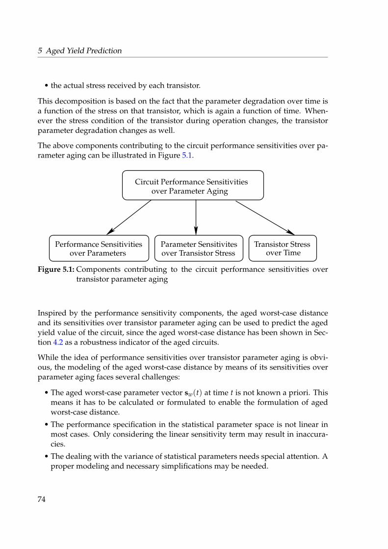
5 Aged Yield Prediction
• the actual stress received by each transistor.
This decomposition is based on the fact that the parameter degradation over time isa function of the stress on that transistor, which is again a function of time. When-ever the stress condition of the transistor during operation changes, the transistorparameter degradation changes as well.
The above components contributing to the circuit performance sensitivities over pa-rameter aging can be illustrated in Figure 5.1.
over Parameters
Circuit Performance Sensitivitiesover Parameter Aging
Parameter Sensitivitesover Transistor Stress
Transistor Stressover Time
Performance Sensitivities
Figure 5.1: Components contributing to the circuit performance sensitivities overtransistor parameter aging
Inspired by the performance sensitivity components, the aged worst-case distanceand its sensitivities over transistor parameter aging can be used to predict the agedyield value of the circuit, since the aged worst-case distance has been shown in Sec-tion 4.2 as a robustness indicator of the aged circuits.
While the idea of performance sensitivities over transistor parameter aging is obvi-ous, the modeling of the aged worst-case distance by means of its sensitivities overparameter aging faces several challenges:
• The aged worst-case parameter vector sw(t) at time t is not known a priori. Thismeans it has to be calculated or formulated to enable the formulation of agedworst-case distance.
• The performance specification in the statistical parameter space is not linear inmost cases. Only considering the linear sensitivity term may result in inaccura-cies.
• The dealing with the variance of statistical parameters needs special attention. Aproper modeling and necessary simplifications may be needed.
74

5.1 Aged Worst-Case Distance Prediction Model
The purpose of the proposed aged yield prediction model is to provide circuit de-signers a quick overview of the quality of their circuits after transistors degrade forsome time, since the fresh worst-case distance is already available for a fresh-optimaldesign. After such a quick circuit reliability evaluation, degradation-sensitive perfor-mances can be identified, certain weakness in the lifetime robustness of their designscan be obtained early and quickly, proper design techniques can be applied to im-prove it, and the cost and time for the circuit design process towards reliability canbe reduced.
5.1 Aged Worst-Case Distance Prediction Model
5.1.1 Idea
In this section, a prediction model of the aged worst-case distance in time domainis presented to speed up the analysis of corresponding the aged yield value. Onlyperformance and statistical parameter sensitivity analysis are needed, in comparisonto the Monte-Carlo simulation method and numerical optimization solutions. It isbased on the linear performance model as follows. The index i of ith performance invector f is left out for simplicity. Without loss of generality, only upper bound fU isconsidered hereafter. The case for lower bound fL can be derived similarly taken thedifferent sign into consideration.
5.1.2 Linear Performance Model at t1
At any time t1 during the operating lifetime, the first-order Taylor expansion of per-formance f (t1) with respect to s(t1) from the worst-case statistical parameter vectorsw,U(t1) in the statistical parameter space is
f (t1) = f (sw,U(t1)) +∇ f (sw,U(t1))T · (s(t1)− sw,U(t1)) (5.1)
By assuming a linear performance model, the sensitivity of performance over statis-tical parameters keeps constant, i.e.,
∇ f (sw,U(t1)) ≡ g (5.2)
is constant over the entire statistical parameter space at any time.
75

5 Aged Yield Prediction
s2
As
s1
g
agings0(t0)
s0(t1)
sw,U(t0)
sw,U(t1)
fU
Figure 5.2: Linear performance model in the statistical parameter space.
f (sw,U(t1)) in (5.1) is the upper bound value fU. So from (5.1) the linear performancemodel at t1 can be formulated as
f (t1) = fU + gT · (s(t1)− sw,U(t1)) (5.3)
The worst-case statistical parameter vector sw,U(t1) is the statistical parameter vectorwhere the corresponding performance f reaches its boundary value fU at t1. It cor-responds to the position in the statistical parameter space where the probability ofoccurrence reaches its maximum in the non-acceptance region (slashed area in Fig-ure 5.2). A robust design indicates that such a probability of occurrence should bekept minimum, i.e., sw,U(t1) should be positioned furthest away from s0(t1) so that itis least sensitive to the changes of statistical parameters which may cause it fall intothe non-acceptance region.
Since s(t1) ∼ N (s0(t1), C(t1)), the mean and the variance of the linearized perfor-mance model can be formulated from (5.3) as
µ( f (t1)) = fU + gT · (s0(t1)− sw,U(t1)) (5.4)σ2
f (t1)= gT ·C · g ≡ σ2
f (5.5)
where (5.5) is constant over time. Taking the process variation as second order effectson the sensitivity towards degradation, C(t1) is assumed to be constant, i.e., C(t1) =C [SRRP09].
76

5.1 Aged Worst-Case Distance Prediction Model
5.1.3 Mapping from t0 to t1
Considering parameter aging from t0 to t1, a first-order Taylor approximation ofµ( f (t1)) with respect to t from t0 can be expressed as
µ( f (t1)) = µ( f (t0)) +∂µ f
∂t|t0 · (t− t0) (5.6)
From (5.4) we have
µ( f (t0)) = fU + gT · (s0(t0)− sw,U(t0)) (5.7)
and∂µ f
∂t|t0 = gT ·
(∂s0(t)
∂t|t0 −
∂sw,U(t)∂t
|t0
)(5.8)
It can be observed from (5.8) that the product
gT · ∂sw,U(t)∂t
|t0 (5.9)
remains zero, since the two vectors g and ∂sw,U(t)∂t |t0 are orthogonal to each other. This
is easy to understand because during the aging of statistical parameters, from t0 tot1, the worst-case statistical parameter vector sw,U(t) moves along the performanceboundary fU, as can be observed in Figure 5.2, while the performance gradient galways points to the direction that is vertical to the performance boundary in thestatistical parameter space. Thus g is orthogonal to the vector ∂sw,U(t)
∂t |t0 , which ispointing in parallel to the performance boundary.
So (5.8) becomes∂µ f
∂t|t0 = gT · ∂s0(t)
∂t|t0 (5.10)
and (5.6) can be further expressed as
µ( f (t1)) ≈ fU + gT · (s0(t0)− sw,U(t0)) + gT · ∂s0(t)∂t|t0 · (t1 − t0) (5.11)
5.1.4 Prediction of βw,U(t1)
The prediction of the aged worst-case distance at t1 requires the mapping of theworst-case distance from t0 to t1 based on sensitivity analysis, in which the results
77

5 Aged Yield Prediction
from section 5.1.3 are needed. The key concept here is to properly derive the sensi-tivity parts concerning the aging of the nominal and worst-case statistical parametervectors.
To predict βw,U(t1), a first-order Taylor expansion of βw,U(t1) with respect to t fromt0 is
βw,U(t1) ≈ βw,U(t0) +dβw,U(t)
dt|t0 · (t− t0) (5.12)
where the sensitivity part, dβw,U(t)dt |t0 can be derived using results from section 5.1.3 as
follows.
Since at the worst-case statistical parameter vector at t1, sw,U(t1), the correspondinglevel contour of s(t1) is
β2w,U(t1) = (sw,U(t1)− s0(t1))
T ·C−1 · (sw,U(t1)− s0(t1)) (5.13)
It touches the performance boundary at sw,U(t1), which means the orthogonal on(5.13) is parallel to g:
C−1 · (sw,U(t1)− s0(t1)) = sign(λ) · λ · g (5.14)
where
sign(λ) ={
+1, µ( f (t1)) ≤ fU ;−1, µ( f (t1)) > fU .
(5.15)
Inserting (5.14) into (5.13) and assuming the positive sign for λ hereafter, we have
β2w,U(t1) = λ2 · gT ·C · g (5.16)
By taking λ from (5.16) into (5.14) we obtain
(sw,U(t1)− s0(t1)) =βw,U(t1)√gT ·C · g
·C · g (5.17)
Then (5.17) is taken back into (5.4):
µ( f (t1)) = fU − βw,U(t1) ·√
gT ·C · g (5.18)
so that the worst-case distance at t1 can be expressed as
βw,U(t1) =fU − µ( f (t1))√
gT ·C · g(5.19)
78
5.1 Aged Worst-Case Distance Prediction Model
Then from (5.19) and (5.11), and applying the results from (4.12), the worst-case dis-tance degradation rate in (5.12) can be formulated as
dβw,U(t)dt
|t0 = −1σf· gT · ∂s0(t)
∂t|t0 (5.20)
which differs from (5) in [SRRP09].
From (5.20) it is clear that the evaluation of the worst-case distance degradation ratefor a performance upper bound involves only multiple sensitivity evaluations whichcan be carried out efficiently. Especially in the context of this thesis, both σf and gremain constant, requiring an one-time evaluation only. The sensitivity of s0(t) overt is calculated by the finite-difference approximation.
In the finite-difference approximation, for a function f of x, f (x), the sensitivity of fover x, f ′(x), is approximated by
f ′(x) ≈ f (x +4x)− f (x)4x
(5.21)
The values of s0(t) at various ages are obtained from the aging simulator described inSection 4.3.1, then the corresponding sensitivity and the worst-case distance degra-dation rate can be evaluated.
Thus, by taking (5.20) back into (5.12), the values of βw,U(t1) at time t1 can be pre-dicted efficiently without searching for the worst-case statistical parameter vectorsw,U(t1) through iterative optimization method.
5.1.5 Second Order Sensitivity Term
The above prediction model for the aged worst-case distance can be further extendedby building up a quadratic prediction model. It is formulated by second-order Taylorexpansion in time domain as:
βw,U(t1) ≈ βw,U(t0) +dβw,U(t)
dt|t0 · (t1 − t0) +
12· d2βw,U(t)
dt2 |t0 · (t1 − t0)2 (5.22)
The additional second-order sensitivity term of the worst-case distance over time in
(5.22), d2βw,U(t)dt2 |t0 , can be obtained by the formulation of µ( f (t1)) in (5.4) and βw,U(t1)
in (5.19) asd2βw,U(t)
dt2 |t0 = −1σf· gT · ∂2s0(t)
∂t2 |t0 (5.23)
79

5 Aged Yield Prediction
The second-order sensitivity of statistical parameters over time, ∂2s0(t)∂t2 |t0 , captures
the fact that the degradation models of most statistical parameters are non-linear intime domain [McP07]. Multiplicated by the performance sensitivity over statisticalparameters, (5.23) can better capture the non-linear effects during the prediction ofthe aged worst-case distance.
5.2 Algorithm for the Aged Yield Prediction
This section presents the structure of the algorithm to predict the aged worst-case dis-tance values and the corresponding aged yield values based on the above proposedprediction models.
choose one performance f with its specification fU, let j = 0 (I)
calculate βw,U(tj) of f using geometric yield approximation (II)
calculate g and σf of f using (5.5) (III)
increase j by 1 (IV)
sensitivity analysis for ∂s0(tj)/∂tj from finite-difference approximation (V)
sensitivity analysis for ∂2s0(tj)/∂t2j from finite-difference approximation (VI)
calculate dβw,U(tj)/dtj using (5.20) and d2βw,U(tj)/dt2j using (5.23) (VII)
predict βw,U(tj) using (5.22) (VII)
predict YU(tj) using (4.61) (VIII)
until j = jmax (IX)
finish (X)
Figure 5.3: Overview of the algorithm to predict aged worst-case distances and agedyield for one of the performance at different ages
Firstly, the worst-case distances βw,U(t0) for one performance feather f at t0 is calcu-lated, using geometric yield approximation method in Chapter 4. In practice, sincethe fresh yield optimization is a necessary step during the circuit design process,these βw,U(t0) can be obtained from the results of the fresh yield optimization.
80
5.3 Summary
Then, the standard deviation of the linear performance model, σf , as well as the sen-sitivity of f over statistical parameters s are prepared. Again, these values are alreadyavailable during the fresh yield analysis based on worst-case distance process.
For each time point tj of interests, the sensitivity analysis of s0(tj) over time is per-formed based on the finite difference approximation. The results of these first-ordersensitivities are then applied into the calculation of second-order sensitivity of s0(t)over time. Based on these results, the first- and second-order sensitivity of βw,U(t)over time can be obtained, using (5.20) and (5.23) respectively. Finally, the agedworst-case distance βw,U(tj) can be predicted. The corresponding aged yield valueYU(tj) can be obtained accordingly.
The degradation of the aged worst-case distance as well as aged yield can then beobtained if the above process is repeated for all of the time points of interests. Thewhole structure of the prediction algorithm is shown in Figure 5.3.
5.3 Summary
Considering both manufacturing process variations and transistor aging during life-time operation, this chapter proposes a modeling and prediction framework to pre-dict the aged worst-case distance value and the corresponding lifetime robustness ofanalog circuits. The proposed method is based on the sensitivity analysis of transis-tor parameters over aging, as well as the sensitivity analysis of the circuit robustnessover transistor parameters. It does not involve either analytical formulation of circuitperformance or Monte-Carlo simulations. In comparison with the aged yield analysisbased on the geometrical yield modeling presented in the last chapter, the proposedmethod is more efficient in obtaining the aged worst-case distance values. Using theproposed method, circuit designers can obtain quickly an overview of the lifetime ro-bustness of their designs, since the fresh worst-case distance is already available fora fresh-optimal design. Certain weakness in the lifetime robustness of their designscan be obtained early and quickly, thus reducing the redesign cost.
81


Chapter 6
Experimental Results
This chapter presents the experimental results on the proposed sizing flow presentedin Chapter 4, as well as the results on the new prediction framework presented inChapter 5. The experiments are performed on different types of operational ampli-fiers, which serve as basic building blocks in analog circuitry. They are based on an180nm industrial technology.
The experiments are run on a 64-bit Linux server with eight 2.33GHZ Xeon CPUs and2G memory. The AgeMOS model parameters are obtained from an industry partner.By using the RelXpert simulator, which has both NBTI and HCI degradation models,the aged BSIM modelcard and the aged netlist for a specific time and temperaturecan be generated. Other types of aging simulators with respective aging models canbe applied as well.
6.1 Miller Operational Amplifier
6.1.1 Circuit Topology
Figure 6.1 shows the schematic of the two-stage Miller operational amplifier used inour experiments [LS94]. The first stage of the circuit is made up of a pair of PMOStransistors with the current mirror MN1 and MN2 as an active load. The second stageis a CMOS inverter with MN3 as driver and MP5 as an active load. The compensatingcapacitor Cmiller connects the output of the circuit to the input.
83

6 Experimental Results
Vss
MP3 MP4
MP1 MP2
MP5
MN1 MN2
MN3
Cmiller
ibias
vin− vin+vout
Vdd
Figure 6.1: Circuit schematic of the Miller operational amplifier
6.1.2 Circuit Performances and their Specifications
In this study, there are seven performance specifications totally for the Miller opera-tional amplifier, as listed in Table 6.1.
Table 6.1: List of performance specifications for the Miller operational amplifier.
Performance DC Gain GBW PM SR CMRR Swing
(dB) (MHz) (degree) (v/µs) (dB) (%)
Specification ≥ 80 ≥ 2 ≥ 60 ≥ 3 ≥ 80 ≥ 90
For the discussion of the experimental results from circuit simulation later, the ana-lytical form of each performance is prepared here first. A complete process of deriva-tions can be referred to [LS94].
• DC GainDC Gain specifies the low frequency gain of the amplifier. It is a major perfor-mance of an amplifier which implies the ability of the amplification. For the firststage, its gain A1 is given by
A1 =gm1
go1(6.1)
84

6.1 Miller Operational Amplifier
where gm1 is the transconductance of transistor MP1, go1 = goMP2 + goMN2 is theload conductance of the first stage. For the second stage which is an inverter, itsgain A2 is given by
A2 =gm3
go2(6.2)
where gm3 is the transconductance of transistor MN3, go2 = goMN3 + goMP5 is theload conductance of the second stage. Then the DC Gain at low frequencies isgiven by
DC Gain = A1A2 =
(gm1
go1
)(gm3
go2
)(6.3)
• GBWGain-Bandwidth product (GBW) is the frequency value at which the gain dropsto 0dB. As the name implies, it can also be defined as the product of the DCGain and the bandwidth. Here, the "bandwidth" of the amplifier refers to thedominant pole frequency, at which the gain starts to drop (more exactly, drops by-3dB). As a constant value with various gain and its frequency, GBW describesthe amplifier’s gain behavior with frequency. For example, if DC Gain is 10000,or 20 log(10000) = 80dB, and GBW is 2MHz, the bandwidth then is 200Hz (atthis frequency the gain is actually (80-3=77)dB). When the gain drops to 1, or0dB, the corresponding frequency is 2MHz. GBW helps the designers to knowthe bandwidth value for a certain gain. A larger GBW implies a wider frequencyat which the maximal gain can be obtained.Analytically, since the dominant pole comes from the result of the Miller effect ofCmiller, the bandwidth can be approximated by
bandwidth ≈ go1
2πA2Cmiller(6.4)
GBW can be obtained by the product of (6.4) and DC Gain, given by (6.3), ap-proximately as
GBW ≈ go1
2πA2Cmiller·(
gm1
go1
)· A2 (6.5)
=go1
2πCmiller(6.6)
• PMPhase margin (PM) is an important indicator of the stability of the amplifier. Sincethe frequency where the gain drops to 0dB is represented as GBW, PM measuresthe difference between the phase at the frequency GBW and −180◦, shown as
PM = ϕ( f = GBW)− (−180◦) (6.7)
85

6 Experimental Results
• SRSlew rate (SR) is the slope of the ramp at the output node of the amplifier whena large input step signal is applied. It has both rising and falling parts. In thisstudy, only the rising slew rate is considered. SR measures how fast the outputsignal follows the input signal. It is measured as
SR = max(
∆Vout
∆T
)(6.8)
i.e., the maximum ratio between the change of the output voltage and the timerequired to achieve such a change.In the two-stage Miller amplifier, it is expressed as
SR =IB
Cmiller(6.9)
where IB is the current flowing through the Miller capacitor to charge it. It arisesfrom the fact that the slewing phenomena occurs when a constant output currentof the first stage charges the compensating capacitor of the second stage. Thelow pass character of the second stage behaves similar to an integrator, where anincreasing output is produced when a constant input is applied.
• CMRRCommon mode rejection ratio (CMRR) is the ratio between amplifier’s differen-tial gain and common mode gain. Ideally, the common mode gain should be zero,since the goal of a differential amplifier with a differential pair as the input stageis to amplify only the differential component of the input signal, while reject to-tally the common-mode component. The resulting CMRR should be infinite inthe ideal case. But in reality, due to the finite output impedance of the currentsource of the differential input stage, as well as the asymmetries in the input pair,it is a finite value. The computation of CMRR, in dB, is given by
CMRR = 20 · log |Adi f f
Acomm| (6.10)
= 20 · log[gm1
go1· 2gmn1Ro] (6.11)
where gm1 is the transconductance of MP1, go1 = goMP2 + goMN2 is the load con-ductance of the first stage, gmn1 is the transconductance of MN1, Ro is the outputresistance of the current source MN1 and MN2. CMRR can be improved by in-creasing the input transconductance gm1, and by taking a current source withhigh output resistance Ro.
86

6.1 Miller Operational Amplifier
• SwingSwing at the output node is the maximum voltage range it can achieve. It ismeasured as a relative percent between maximum output voltage and the supplyvoltage. In reality, the maximum output voltage is limited by two factors: Vds ofMP5 which keeps it in saturation, and the output current driving the load. Asmentioned in [Raz01], the maximum voltage swing trades with device size andbias currents and hence speed. It is the principle challenge to obtain a large swingin modern analog design.
6.1.3 Results on Aged Yield Optimization
Table 6.2 shows the result using the proposed fresh circuit optimization and lifetimeyield analysis flow. They are obtained based on circuit simulations. For the fiveperformances considered, the corresponding worst-case distance values as well asthe total yield values for the fresh circuit and the 10-year-old circuit are listed. It isclear from the table that the lifetime robustness of the circuit is ensured, with an agedyield of 96.9% even after 10 years.
Table 6.2: Simulation results of worst-case distance after applying the proposed op-timization flow for the fresh and aged Miller operational amplifier.
t = 0 t = 10 years
DC Gain 4.790 4.470
GBW 5.901 5.720
PM 6.382 6.155
SR 5.441 2.030
CMRR 4.423 2.896
Yield 100% 96.9%
It can be observed from Table 6.2 that the SR and CMRR are critical performancesconsidering aging after 10 years. They are justified as follows.
To measure SR, a positive voltage step is applied to vin+, which turns off the PMOStransistor MP2. The current from the current source MP4 then flows through MP1and MN1, as well as through MN2 as a copy. Since MP2 is off, this current willbe drawn through the capacitor Cmiller. The SR of the amplifier is then determinedby the speed of charging/discharging of this Cmiller. When transistor aging occurs,
87
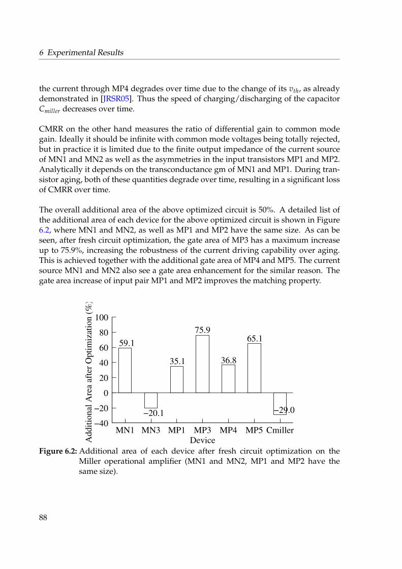
6 Experimental Results
the current through MP4 degrades over time due to the change of its vth, as alreadydemonstrated in [JRSR05]. Thus the speed of charging/discharging of the capacitorCmiller decreases over time.
CMRR on the other hand measures the ratio of differential gain to common modegain. Ideally it should be infinite with common mode voltages being totally rejected,but in practice it is limited due to the finite output impedance of the current sourceof MN1 and MN2 as well as the asymmetries in the input transistors MP1 and MP2.Analytically it depends on the transconductance gm of MN1 and MP1. During tran-sistor aging, both of these quantities degrade over time, resulting in a significant lossof CMRR over time.
The overall additional area of the above optimized circuit is 50%. A detailed list ofthe additional area of each device for the above optimized circuit is shown in Figure6.2, where MN1 and MN2, as well as MP1 and MP2 have the same size. As can beseen, after fresh circuit optimization, the gate area of MP3 has a maximum increaseup to 75.9%, increasing the robustness of the current driving capability over aging.This is achieved together with the additional gate area of MP4 and MP5. The currentsource MN1 and MN2 also see a gate area enhancement for the similar reason. Thegate area increase of input pair MP1 and MP2 improves the matching property.
−20.1−20
0
20
40
60
80
100
MN1 MN3 MP1 MP3 MP4 MP5 CmillerDeviceA
ddit
ional
Are
a af
ter
Opti
miz
atio
n (
%)
59.1
35.1
75.9
36.8
65.1
−29.0
−40
Figure 6.2: Additional area of each device after fresh circuit optimization on theMiller operational amplifier (MN1 and MN2, MP1 and MP2 have thesame size).
88
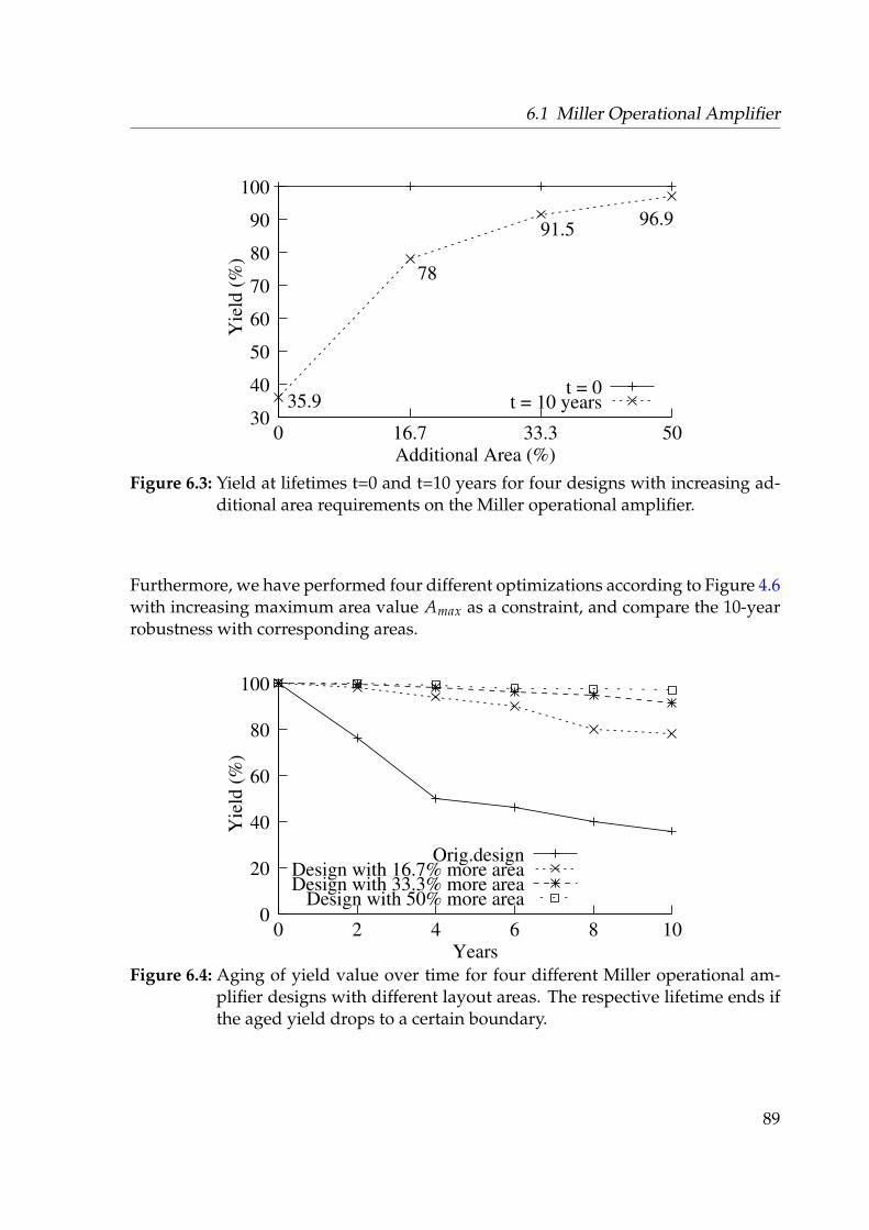
6.1 Miller Operational Amplifier
16.7 33.3 50Additional Area (%)
91.5
78
35.9
96.9Y
ield
(%
)
30
40
50
60
t = 10 years
70
80
90
100
0
t = 0
Figure 6.3: Yield at lifetimes t=0 and t=10 years for four designs with increasing ad-ditional area requirements on the Miller operational amplifier.
Furthermore, we have performed four different optimizations according to Figure 4.6with increasing maximum area value Amax as a constraint, and compare the 10-yearrobustness with corresponding areas.
80
100
0
Design with 16.7% more area
2 4 6 8 10Years
Orig.design 20
Design with 33.3% more area
0
Yie
ld (
%)
Design with 50% more area
40
60
Figure 6.4: Aging of yield value over time for four different Miller operational am-plifier designs with different layout areas. The respective lifetime ends ifthe aged yield drops to a certain boundary.
89

6 Experimental Results
Figure 6.3 shows the results for the fresh and 10-year-old circuit. As can be seen,a bigger aged yield value always requires more circuit area. In comparison to aninitial design which achieves an optimized 10 years yield value of 35.9%, it needs16.7% more area for an optimized aged yield value of 78%, or 33.3% more area for anoptimized aged yield value of 91.5%, or 50% more area for 96.9% aged yield.
Figure 6.4 shows the aging of yield values from their fresh value to various timepoints for the above four different designs with different layout area. It is clear fromthe figure that, concerning the aged yield values, the design with 50% more area isthe most robust one which ages relatively slowly in comparison to other realizations.
The aged yield value indicates the aged robustness of the circuit. When it dropsto a certain pre-defined value, the lifetime of the circuit products according to thatdefinition ends. The above experimental results verify that a longer circuit lifetimerequires more total area to be spent in layout. By using the proposed sizing flow withmaximum area constraints, designers can ensure the circuit robustness in operationallifetime with a certain layout area consumption.
6.1.4 Results on Aged Yield Prediction
To verify the prediction model presented in Chapter 5 on the Miller operational am-plifier, the aged worst-case distance values obtained through a geometric aged yieldanalysis based on the evaluation of aged worst-case distances by solving (4.74), andthrough the prediction model (5.22) are compared for the five performances listed inTable 6.2. The comparison results are presented in Table 6.3.
Table 6.3: Aged worst-case distance prediction results in comparison with accuratevalues for different performance features of the Miller operational ampli-fier at t=10 years.
Accurate Predict Error Speedup
DC Gain 4.470 4.602 3.0% 4.6X
GBW 5.720 5.362 6.3% 6.5X
PM 6.155 6.348 3.1% 6.2X
SR 2.030 2.124 4.6% 6.5X
CMRR 2.896 2.630 9.2% 7.4X
Average 5.24% 6.22X
90

6.1 Miller Operational Amplifier
As can be seen from the table, for the five performances considered, the predictedaged worst-case distances match very close to the accurate aged worst-case distancevalues, with an average error of 5.24%. A clear speedup by using the proposed pre-diction framework can be observed. On average they are 6.22 times faster in compar-ison to the solutions obtained through the geometric aged yield analysis.
A detailed comparison on prediction results and relative errors at various time pointsof interests for the performance SR and CMRR are plotted in Figure 6.5. It is clearfrom the figure that the results using the proposed prediction framework can welltrack the aging of the worst-case distances at multiple time points of interests duringthe lifetime. As a result, circuit designers can have a quick image of their design ro-bustness with relatively small error by applying the proposed prediction framework.
2.2
2.3
2.4
2.5
2.6
2.7
2.8
1.0E+01 1.0E+03 1.0E+05 1.0E+07
Aged
wors
t−ca
se d
ista
nce
of
SR
Time (s)
Predict 2
2.1 Accurate
(a)
Time (s)
0.02
0.04
0.06
0.08
0.1
1.0E+01 1.0E+03 1.0E+05 1.0E+07
Rela
tive e
rror
0
(b)
3
3.2
3.4
3.6
3.8
4
4.2
1.0E+01 1.0E+03 1.0E+05 1.0E+07Aged
wors
t−ca
se d
ista
nce
of
CM
RR
Time (s)
Predict 2.4
2.6
2.8Accurate
(c)
Time (s)
0.06
0.07
0.08
0.09
0.1
0.11
0.12
0.13
0.14
0.15
1.0E+01 1.0E+03 1.0E+05 1.0E+07
Rela
tive e
rror
0.05
(d)
Figure 6.5: Comparison results of βw(t) at respective time points for SR (a) andCMRR (c), and the corresponding relative errors for SR (b) and CMRR(d) of the Miller operational amplifier.
91
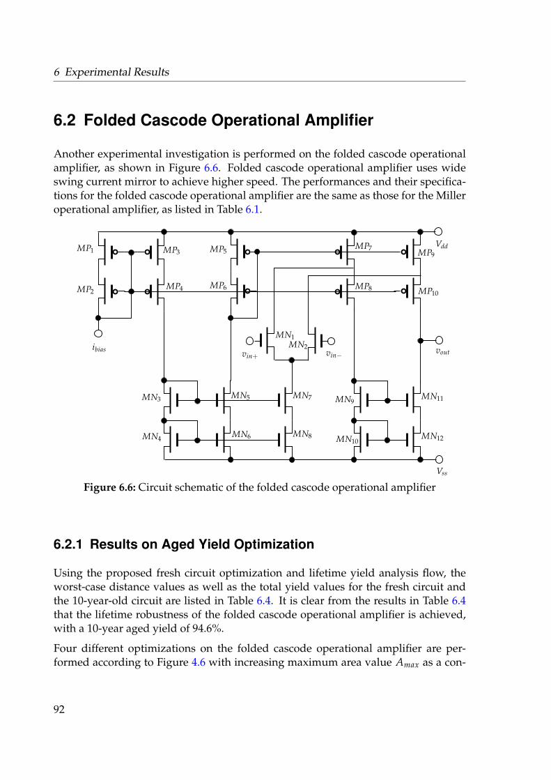
6 Experimental Results
6.2 Folded Cascode Operational Amplifier
Another experimental investigation is performed on the folded cascode operationalamplifier, as shown in Figure 6.6. Folded cascode operational amplifier uses wideswing current mirror to achieve higher speed. The performances and their specifica-tions for the folded cascode operational amplifier are the same as those for the Milleroperational amplifier, as listed in Table 6.1.
MN12
Vdd
Vss
voutibias vin+ vin−
MP1
MP2
MP3
MP4
MP5
MN1MN2
MP6
MP7
MP8
MP9
MP10
MN3
MN4
MN5
MN6
MN7
MN8
MN9
MN10
MN11
Figure 6.6: Circuit schematic of the folded cascode operational amplifier
6.2.1 Results on Aged Yield Optimization
Using the proposed fresh circuit optimization and lifetime yield analysis flow, theworst-case distance values as well as the total yield values for the fresh circuit andthe 10-year-old circuit are listed in Table 6.4. It is clear from the results in Table 6.4that the lifetime robustness of the folded cascode operational amplifier is achieved,with a 10-year aged yield of 94.6%.
Four different optimizations on the folded cascode operational amplifier are per-formed according to Figure 4.6 with increasing maximum area value Amax as a con-
92

6.2 Folded Cascode Operational Amplifier
Table 6.4: Simulation results of worst-case distance after applying the proposed opti-mization flow for the fresh and aged folded cascode operational amplifier.
t = 0 t = 10 years
DC Gain 4.761 4.289
GBW 6.372 5.837
PM 7.760 6.219
SR 5.280 2.873
CMRR 5.095 1.914
Yield 100% 94.6%
16.7 33.3 50Additional Area (%)
52.2
74
87
94.6
Yie
ld (
%)
30
40
50
60
t = 10 years
70
80
90
100
0
t = 0
Figure 6.7: Yield at lifetimes t=0 and t=10 years for four designs with increasing ad-ditional area requirements on the folded cascode operational amplifier.
straint. The trade-off between the 10-year robustness and the corresponding areas ofthe four designs are presented in the following.
Figure 6.7 shows the results for the fresh and 10-year-old circuit. As can be seen,a bigger aged yield value always requires more circuit area. In comparison to aninitial design which achieves an optimized 10 years yield value of 52.2%, it needs16.7% more area for an optimized aged yield value of 74%, or 33.3% more area for anoptimized aged yield value of 87%, or 50% more area for 94.6% aged yield.
93

6 Experimental Results
40
60
80
Design with 16.7% more area
100
0 2 4 6 8
Orig.design
10
Design with 33.3% more area
Years
Yie
ld (
%)
Design with 50% more area 0
20
Figure 6.8: Aging of yield value over time for four different folded cascode opera-tional amplifier designs with different layout areas. The respective life-time ends if the aged yield drops to a certain boundary.
Figure 6.8 shows the aging of yield values from their fresh value to various timepoints for the above four different designs. The experimental results on the foldedcascode operational amplifier also verify the fact that, spending more layout areacan ensure a better lifetime robustness of the circuits. By using the proposed sizingflow with maximum area constraints, designers can ensure the circuit robustness inoperational lifetime with a certain layout area consumption.
6.2.2 Results on Aged Yield Prediction
To verify the prediction model presented in Chapter 5 on the folded cascode opera-tional amplifier, the aged worst-case distance values obtained through the geometricaged yield analysis based on the evaluation of aged worst-case distances by solv-ing (4.74), and through the prediction model (5.22) are compared for the five perfor-mances listed in Table 6.4. The comparison results are presented in Table 6.5.
As can be seen from the table, for the five performances considered on the foldedcascode operational amplifier, the predicted aged worst-case distances also matchvery close to the accurate aged worst-case distance values, with an average errorof 6.10%. A clear speedup by using the proposed prediction framework can alsobe observed in this case, with an average value of 5.98 times in comparison to thesolutions obtained through the geometric aged yield analysis.
94

6.2 Folded Cascode Operational Amplifier
Table 6.5: Aged worst-case distance prediction results in comparison with accuratevalues for different performance features of the folded cascode operationalamplifier at t=10 years.
Accurate Predict Error Speedup
DC Gain 4.289 4.590 4.9% 4.2X
GBW 5.837 5.984 2.5% 6.8X
PM 6.219 6.618 6.4% 5.7X
SR 2.873 2.684 6.6% 6.3X
CMRR 1.914 1.720 10.1% 6.9X
Average 6.10% 5.98X
2.9
3
3.1
3.2
3.3
3.4
3.5
1.0E+01 1.0E+03 1.0E+05 1.0E+07
Aged
wors
t−ca
se d
ista
nce
of
SR
Time (s)
Predict 2.7
2.8 Accurate
(a)
Time (s)
0.02
0.04
0.06
0.08
0.1
1.0E+01 1.0E+03 1.0E+05 1.0E+07
Rela
tive e
rror
0
(b)
Predict 2
2.5
3
3.5
4
4.5
1.0E+01 1.0E+03 1.0E+05 1.0E+07Aged
wors
t−ca
se d
ista
nce
of
CM
RR
Time (s)
Accurate
(c)
Time (s)
0.06
0.07
0.08
0.09
0.1
0.11
0.12
0.13
0.14
0.15
1.0E+01 1.0E+03 1.0E+05 1.0E+07
Rela
tive e
rror
0.05
(d)
Figure 6.9: Comparison results of βw(t) at respective time points for SR (a) andCMRR (c), and the corresponding relative errors for SR (b) and CMRR(d) of the folded cascode operational amplifier.
95

6 Experimental Results
A detailed comparison on prediction results and relative errors at various time pointsof interests for the performance SR and CMRR are plotted in Figure 6.9. It is clearfrom the figure that for the folded cascode operational amplifier, the results usingthe proposed prediction framework can also well track the aging of the worst-casedistances at multiple time points of interests during the lifetime. Thus the proposedframework to predict the aged worst-case distance serves as a fast overview into thelifetime robustness of the circuits.
6.3 Summary
This chapter presents the experimental results of the proposed fresh circuit optimiza-tion and lifetime yield analysis flow, as well as the modeling and prediction frame-work to predict the aged worst-case distance value and the corresponding lifetimerobustness of analog circuits. According to the result of this trade-off analysis, alonger circuit lifetime requires more total area to be spent in layout, and designerscan ensure the circuit robustness with certain layout area consumption. The resultson the aged worst-case distance prediction models, on the other hand, verify that themodels are accurate enough to provide a fast overview of the lifetime robustness ofthe analog circuits.
96

Chapter 7
Conclusion
Semiconductor manufacturing process variations and transistor aging during life-time operations are the two main challenges raised by the continuous scaling of semi-conductor technologies. Although the higher chip density with a lower cost per tran-sistor as well as the improved circuit performance are contributed by the advancedtechnologies, designers must ensure the robustness of their circuit designs early dur-ing the design phase to tolerate those above mentioned uncertainties. This task isgetting more and more complicated with increased number of transistor parametersand design complexities in the new generations of technologies.
In comparison to the digital counterpart, the design of analog integrated circuits isstill mainly done manually. However, there has been a trend in recent years towardsan automatic sizing of analog integrated circuits, by the close interaction betweenanalog designers and automatic sizing software tools. These tools can help analogdesigners in improving their design qualities with a better overview of the designspace and a more intelligent recognition of important analog circuit structures, aswell as a better solution in terms of sizing. In addition, these automatic sizing toolsneed to consider the emerging effects caused by the new manufacturing technologiesand physical effects in order to improve the quality of the solutions they provideto the designers. Thus there is a strong need from the semiconductor industry forboth analog circuit designers and automatic sizing tool developers, to have a betterunderstanding into the emerging reliability challenges and deeper improvement inthe whole design flow to cope with the new physical effects.
This thesis proposes new solutions to the joint effects of process variations and tran-sistor aging, with new sizing flow during design phase to ensure a robust circuit de-sign in operational lifetime, as well as a new prediction framework to help designersevaluate their design robustness in operational lifetime.
97

7 Conclusion
The new sizing flow presented in Chapter 4 is based on the evaluation and optimiza-tion of the worst-case distance for fresh circuits with checking of sizing rules for bothfresh and aged circuits. The worst-case distance has been proved to be an effectivemeasurement to the circuit robustness in terms of a number of sigma. Originatedfor the modeling of statistical manufacturing process variations, worst-case distancealso applies in the case where the statistical parameters drift over time due to tran-sistor aging. Thus the evaluation of the fresh and aged worst-case distance providesinsights into the circuit robustness for both fresh and aged circuits. Checking of siz-ing rules for both fresh and aged circuits, on the other hand, ensures the robustnessfurther into lifetime operation, since certain constraints on transistor node voltagesare ensured in the sizing flow. Overall, the proposed flow captures the robustnessmeasures based on fresh and aged worst-case distances, optimize the fresh worst-case distances, with consideration of both fresh and aged sizing rules to ensure thelifetime robustness.
The new prediction framework presented in Chapter 5 further speeds up the evalua-tion of the aged circuit robustness. The prediction of the aged worst-case distance, inthis case, is based on an analytical evaluation model, instead of the solution from aniterative numerical optimization algorithm. The sensitivity analysis of the statisticalparameters over time is obtained using aging simulators with specified time points ofinterests. It does not involve either analytical formulation of circuit performances orMonte-Carlo simulations. Circuit designers can capture quickly an overview of thelifetime robustness of their designs, and certain weakness in the lifetime robustnessof their designs can be obtained early and quickly, thus reducing the redesign cost.
In conclusion, the presented methods provide new solutions to the emerging jointeffects of process variations and transistor aging in the scaling semiconductor manu-facturing technologies, with new sizing flow during design phase to ensure a robustcircuit design in operational lifetime, as well as a new prediction framework to helpdesigners to predict their design robustness.
98

Bibliography
[AGW94] K. Antreich, H. Graeb, and C. Wieser. Circuit analysis and optimizationdriven by worst-case distances. IEEE Transactions on Computer-AidedDesign of Integrated Circuits and Systems, 13(1):57–71, 1994.
[AHY87] S. Aur, D.E. Hocevar, and P. Yang. HOTRON-A circuit hot electroneffect simulator. In Proceedings of the IEEE International Conference onComputer-Aided Design (ICCAD), pages 256–259, 1987.
[AKPR07] M. Alam, K. Kang, BC Paul, and K. Roy. Reliability-and process-variation aware design of VLSI circuits. In Proceedings of the 14th IEEEInternational Symposium on the Physical and Failure Analysis of IntegratedCircuits (IPFA), pages 17–25, Bangalore, India, 2007.
[AKVM07] M. A. Alam, H. Kufluoglu, D. Varghese, and S. Mahapatra. A compre-hensive model for PMOS NBTI degradation: Recent progress. Micro-electronics Reliability, 47(6):853–862, June 2007.
[AMHH99] Hany L. Abdel-Malek, Abdel-Karim S. O. Hassan, and Mohamed H.Heaba. A boundary gradient search technique and its applications indesign centering. IEEE Transactions on Computer-Aided Design of Inte-grated Circuits and Systems, 18(11):1654–1660, November 1999.
[AS94] S. A. Aftab and M. A. Styblinski. IC variability minimization usinga new Cp and Cpk based variability/performance measure. In Proceed-ings of the IEEE International Symposium on Circuits and Systems (ISCAS),pages 149 – 152, London , UK, May 1994.
[AVK08] M.A. Alam, D. Varghese, and B. Kaczer. Theory of breakdown positiondetermination by voltage-and current-ratio methods. IEEE Transactionson Electron Devices, 55(11):3150–3158, 2008.
[AWS02] M.A. Alam, B.E. Weir, and P.J. Silverman. A study of soft and hardbreakdown-Part II: Principles of area, thickness, and voltage scaling.IEEE Transactions on Electron Devices, 49(2):239–246, 2002.
[Bak08] R. Jacob Baker. CMOS circuit design, layout and simulation. IEEE Press,John Wiley & Sons, Inc., 2nd edition, 2008.
99

Bibliography
[BC10] Robert Brayton and Jason Cong. NSF Workshop on EDA: Past, Present,and Future. IEEE Design & Test of Computers, 27(3):62–74, May-June2010.
[BGT81] Robert G. Bland, Donald Goldfarb, and Michael J. Todd. The ellipsoidmethod: a survey. Operational Research, 29(6):1039–1091, November-December 1981.
[BJ77] Peter W. Becker and Finn Jensen. Design of Systems and Circuits forMaximum Reliability or Maximum Production Yield. McGraw-Hill BookCompany, 1977.
[Bla69] J.R. Black. Electromigration – A brief survey and some recent results.IEEE Transactions on Electron Devices, 16(4):338–347, 1969.
[cad] http://www.cadence.com.
[CCL+03] G. Chen, K. Y. Chuah, M. F. Li, D. S. H. Chan, C. H. Ang, J. Z. Zhcng,Y. Jin, and D. L. Kwong. Dynamic NBTI of pMOS transistors and its im-pact on device lifetime. In Proceedings of International Reliability PhysicsSymposium, pages 196–202, 2003.
[CFSL10] F.R. Chouard, M. Fulde, and D. Schmitt-Landsiedel. Reliability assess-ment of voltage controlled oscillators in 32nm high-κ metal gate tech-nology. In Proceedings of the 2010 European Solid-State Circuits Conference(ESSCIRC), pages 410–413, Seville, Spain, 2010.
[CGRP09] Ashutosh Chakraborty, Gokul Ganesan, Anand Rajaram, and David Z.Pan. Analysis and optimization of NBTI induced clock skew in gatedclock trees. In Proceedings of the Design, Automation & Test in Europe(DATE), pages 296 – 299, Nice, France, April 2009.
[CMFSL11a] Florian Raoul Chouard, Shailesh More, Michael Fulde, and DorisSchmitt-Landsiedel. An aging suppression and calibration approachfor differential amplifiers in advanced CMOS technologies. In Pro-ceedings of the 2011 European Solid-State Circuits Conference (ESSCIRC),pages 251–254, Helsinki, Finland, 2011.
[CMFSL11b] Florian Raoul Chouard, Shailesh More, Michael Fulde, and DorisSchmitt-Landsiedel. An analog perspective on device reliability in32nm high-κ metal gate technology. In Proceedings of 2011 IEEE In-ternational Symposium on Design and Diagnostics of Electronic Circuits &Systems (DDECS), Cottbus, Germany, 2011.
100

Bibliography
[DG98] Geert Debyser and Georges Gielen. Efficient analog circuit synthesiswith simultaneous yield and robustness optimization. In Proceedingsof IEEE/ACM International Conference on Computer-Aided Design, pages308 – 311, November 1998.
[DGSL09] S. Drapatz, G. Georgakos, and D. Schmitt-Landsiedel. Impact of nega-tive and positive bias temperature stress on 6T-SRAM cells. Advancesin Radio Science, 7:191–196, 2009.
[DH77] S. Director and G. Hachtel. The simplicial approximation approach todesign centering. IEEE Transactions on Circuits and Systems, 24(7):363 –372, July 1977.
[DHGSL10] Stefan Drapatz, Karl Hofmann, Georg Georgakos, and Doris Schmitt-Landsiedel. Impact of fast-recovering NBTI degradation on stability oflarge-scale SRAM arrays. In Proceedings of the 2010 European Solid-StateDevice Research Conference (ESSDERC), pages 146–149, Seville, Spain,2010.
[Die07] B. Dierickx. Scaling below 90nm: Designing with unreliable compo-nents, 2007.
[DK95] Abhijit Dharchoudhury and S. M. Kang. Worst-case analysis and opti-mization of VLSI circuit performances. IEEE Transactions on Computer-Aided Design of Integrated Circuits and Systems, 14(4):481 – 492, April1995.
[DS98] Norman Richard Draper and Harry Smith. Applied Regression Analysis,volume 326 of Wiley Series in Probability and Statistics. Wiley, New York,3rd edition, 1998.
[ea06] I. Ahsan et al. RTA-driven intra-die variations in stage delay, and para-metric sensitivities for 65nm technology. In Symposium on VLSI Tech-nology Digest of Technical Papers, 2006.
[eet] http://eetimes.eu/en/learning-center/automotive-featured.html.
[Esh92] K. Eshbaugh. Generation of correlated parameters for statistical circuitsimulation. IEEE Transactions on Computer-Aided Design, 11(10):1198–1206, 1992.
[FAH+08] Thomas Fischer, Ettore Amirante, Karl Hofmann, Martin Ostermayr,Peter Huber, and Doris Schmitt-Landsiedel. A 65nm test structure forthe analysis of NBTI induced statistical variation in SRAM transistors.In Proceedings of the 2008 European Solid-State Device Research Conference(ESSDERC), pages 51–54, Edinburgh, Scotland, UK, September 2008.
101

Bibliography
[FAH+09] Thomas Fischer, Ettore Amirante, Peter Huber, Karl Hofmann, Mar-tin Ostermayr, and Doris Schmitt-Landsiedel. A 65 nm test structurefor SRAM device variability and NBTI statistics. Solid-State Electronics,53(7):773–778, July 2009.
[Fle87] Roger Fletcher. Practical Methods of Optimization. John Wiley & SonsLtd, second edition, 1987.
[GDWM+08] G. Gielen, P. De Wit, E. Maricau, J. Loeckx, J. Martín-Martínez,B. Kaczer, G. Groeseneken, R. Rodríguez, and M. Nafría. Emergingyield and reliability challenges in nanometer CMOS technologies. InProceedings of the Design, Automation and Test in Europe (DATE), pages1322–1327, Munich, Germany, 2008.
[GP09] Helmut Graeb and Xin Pan. Optimierung integrierter Schaltungen imHinblick auf Alterungseinfluesse. In newsletter edacentrum, pages 11–14, October 2009.
[Gra07] Helmut Graeb. Analog Design Centering and Sizing. Springer, TheNetherlands, 2007.
[GS97] Charles M. Grinstead and J. Laurie Snell. Introduction to Probability.American Mathematical Society, second edition, July 1997.
[GWA93] Helmut E. Graeb, Claudia U. Wieser, and Kurt J. Antreich. Improvedmethods for worst-case analysis and optimization incorporating oper-ating tolerances. In Proceedings of the 30th ACM/IEEE Design AutomationConference, pages 142 – 147, Dallas, Texas, June 1993.
[GZEA01] H. Graeb, S. Zizala, J. Eckmueller, and K. Antreich. The sizing rulesmethod for analog integrated circuit design. In Proceedings of theIEEE/ACM International Conference on Computer-Aided Design, pages343–349, San Jose, CA, USA, 2001.
[HH64] J. M. Hammersley and D. C. Handscomb. Monte Carlo methods. LondonMethuen & Co. Ltd, 1964.
[Hjo80] Urban Hjorth. A reliability distribution with increasing, decreasing,constant and bathtub-shaped failure rates. Technometrics, 22(1):99–107,February 1980.
[HLT83] Dale E. Hocevar, Michael R. Lightner, and Timothy N. Trick. A studyof variance reduction techniques for estimating circuit yields. IEEETransactions on Computer-Aided Design, 2(3):180–192, July 1983.
102
Bibliography
[HTH+85] C. Hu, S.C. Tam, F.C. Hsu, P.K. Ko, T.Y. Chan, and KW Terrill.Hot-electron-induced MOSFET degradation– model, monitor, and im-provement. IEEE Journal of Solid-State Circuits, 20(1):295–305, 1985.
[Hu92] C. Hu. IC reliability simulation. IEEE Journal of Solid-State Circuits,27(3):241–246, 1992.
[I.T] I.T.R.S. International Technology Roadmap for Semiconductors (ITRS).http://www.itrs.net, 2009 edition.
[JRSR05] NK Jha, PS Reddy, DK Sharma, and VR Rao. NBTI degradation andits impact for analog circuit reliability. IEEE Transactions on ElectronDevices, 52(12):2609–2615, 2005.
[JWL82] K. Jain, C. G. Willson, and B. J. Lin. Ultrafast deep UV lithography withexcimer lasers. IEEE Electron Device Letters, 3(3):53–55, March 1982.
[KD95] Kannan Krishna and Stephen W. Director. The linearized performancepenalty (LPP) method for optimization of parametric yield and its reli-ability. IEEE Transactions on Computer-Aided Design of Integrated Circuitsand Systems, 14(12):1557–1568, December 1995.
[KFHR01] M. Karam, W. Fikry, H. Haddara, and H. Ragai. Implementation ofhot-carrier reliability simulation in Eldo. In Proceedings of the IEEE In-ternational Symposium on Circuits and Systems (ISCAS), volume 5, pages515–518, Sydney, NSW , Australia, May 2001.
[Kil] Jack Kilby. Miniaturized electronic circuits. U.S. Patent 3,138,743. Is-sued June 23, 1964 (filed Feb. 6, 1959).
[KKAR06] Kunhyuk Kang, H. Kufluoglu, M. A. Alain, and K. Roy. Efficienttransistor-level sizing technique under temporal performance degra-dation due to NBTI. In Proceedings of the IEEE International Conferenceon Computer Design (ICCD), pages 216–221, San Jose, CA, USA, October2006.
[KKW03] Georgia-Ann Klutke, Peter C. Kiessler, and M. A. Wortman. A criticallook at the bathtub curve. IEEE Transactions on Reliability, 52(1):125–129, March 2003.
[LFG10] Bo Liu, Francisco V. Fernández, and Georges Gielen. An accurate andefficient yield optimization method for analog circuits based on com-puting budget allocation and memetic search technique. In Proceedingsof the Design, Automation and Test in Europe (DATE), pages 1106 – 1111,Dresden, Germany, 2010.
103

Bibliography
[LFJG09] Bo Liu, Francisco V. Fernández, Dimitri De Jonghe, and Georges Gie-len. Less expensive and high quality stopping criteria for MC-basedanalog IC yield optimization. In Proceedings of the 16th IEEE Interna-tional Conference on Electronics, Circuits and Systems (ICECS), pages 267–270, Yasmine Hammamet, Tunis, December 2009.
[Li10] Yan Li. Robust Design of DRAM Core Circuits - Yield Estimation and Anal-ysis by A Statistical Design Approach. Phd thesis, Technische Universi-taet Muenchen, Munich, Germany, 2010.
[Lie06] J. Lienig. Introduction to electromigration-aware physical design. InProceedings of the IEEE International Symposium on Physical Design, 2006.
[LK89] Y. Leblebici and SM Kang. Simulation of MOS circuit performancedegradation with emphasis on VLSI design-for-reliability. In Proceed-ings of the IEEE International Conference on Computer Design (ICCD):VLSI in Computers and Processors, pages 492–495, Cambridge, MA ,USA, Octoboer 1989.
[LMM06] Z. Liu, BW McGaughy, and JZ Ma. Design tools for reliability analysis.In Proceedings of the ACM/IEEE Design Automation Conference (DAC),pages 182–187, San Francisco, CA, USA, 2006.
[LQH+06] X. Li, J. Qin, B. Huang, X. Zhang, and J.B. Bernstein. A new SPICEreliability simulation method for deep submicrometer CMOS VLSI cir-cuits. IEEE Transactions on Device and Materials Reliability, 6(2):247–257,2006.
[LS94] Kenneth R. Laker and Willy M. C. Sansen. Design of Analog IntegratedCircuits and Systems. McGraw-Hill, Inc, 1994.
[LSZ+09] Y. Lu, L. Shang, H. Zhou, H. Zhu, F. Yang, and X. Zeng. Statistical relia-bility analysis under process variation and aging effects. In Proceedingsof the ACM/IEEE Design Automation Conference (DAC), pages 514–519,San Francisco, CA, USA, 2009.
[LWH+07] Hong Luo, Yu Wang, Ku He, Rong Luo, Huazhong Yang, and Yuan Xie.Modeling of PMOS NBTI effect considering temperature variation. InProceedings of the 8th IEEE International Symposium on the Quality Elec-tronic Design (ISQED), pages 139–144, San Jose, CA, USA, March 2007.
[LWM+93] MM Lunenborg, PBM Wolbert, PBL Meijer, T. Phat-Nguyen, andJF VerWeij. Press-a circuit simulator with built-in reliability model for
104

Bibliography
hot-carrier degradation. In Proceedings of the European Symposium on Re-liability of Electron Devices, Failure Physics and Analysis (ESREF), pages157–161, 1993.
[Mas09] Tobias Massier. On the Structural Analysis of CMOS and Bipolar Ana-log Integrated Circuits. Phd thesis, Technische Universitaet Muenchen,Munich, Germany, 2009.
[Mas10] Tobias Massier. On the Structural Analysis of CMOS and Bipolar Ana-log Integrated Circuits. Phd thesis, Technische Universitaet Muenchen,Munich, Germany, 2010.
[McP07] J.W. McPherson. Reliability trends with advanced CMOS scaling andthe implications for design. In Proceedings of the 2007 IEEE CustomIntegrated Circuits Design (CICC), pages 405–412, San Jose, CA, USA,September 2007.
[MDJG12] E. Maricau, D. De Jonghe, and G. Gielen. Hierarchical analog circuitreliability analysis using multivariate nonlinear regression and activelearning sample selection. In Proceedings of the Design, Automation andTest in Europe (DATE), pages 745–750, Dresden, Germany, 2012.
[MFCSL11] Shailesh More, Michael Fulde, Florian Chouard, and Doris Schmitt-Landsiedel. Reducing impact of degradation on analog circuits bychopper stabilization and autozeroing. In Proceedings of the 12th IEEEInternational Symposium on the Quality Electronic Design (ISQED), pages1–6, Santa Clara, CA, USA, 2011.
[MG09] E. Maricau and G. Gielen. Efficient reliability simulation of analogICs including variability and time-varying stress. In Proceedings of theDesign, Automation and Test in Europe (DATE), pages 1238–1241, Nice,France, 2009.
[MG10] E. Maricau and G. Gielen. Variability-aware reliability simulation ofmixed-signal ICs with quasi-linear complexity. In Proceedings of the De-sign, Automation and Test in Europe (DATE), pages 1094–1099, Dresden,Germany, 2010.
[MG11] E. Maricau and G. Gielen. Stochastic circuit reliability analysis. InProceedings of the Design, Automation and Test in Europe (DATE), pages1–6, Grenoble, France, 2011.
[MGS08] T. Massier, H. Graeb, and U. Schlichtmann. The sizing rules methodfor CMOS and bipolar analog integrated circuit synthesis. IEEE Trans-
105

Bibliography
actions on Computer-Aided Design of Integrated Circuits and Systems,27(12):2209–2222, December 2008.
[Ml95] G.E. Mueller-l. PASTA – the characterization of the inherent fluctu-ations in the fabrication process for circuit simulation. Internationaljournal of circuit theory and applications, 23(4):413–432, 1995.
[Moo65] Gordon E. Moore. Cramming more components onto integrated cir-cuits. Electronics, 38(8), April 1965.
[Moo75] Gordon E. Moore. Progress in digital integrated electronics. In Interna-tional Electron Device Meeting, pages 11–13, 1975.
[Nas08] Sani R. Nassif. Process variability at the 65nm node and beyond.In Proceedings of the IEEE Custom Integrated Circuits Conference (CICC),pages 1–8, San Jose, CA, USA, 2008.
[Noy] Robert Norton Noyce. Semiconductor device and lead structure. U.S.Patent 2,981,877. Issued Apr. 25, 1961 (filed July 30, 1959).
[NW00] Jorge Nocedal and Stephen J. Wright. Numerical Optimization. Springer,2000.
[PDW89] Marcel J. M. Pelgrom, Aad C. J. Duinmaijer, and Anton P. G. Welbers.Matching properties of MOS transistors. IEEE Journal of Solid-State Cir-cuits, 24(5):1433–1440, October 1989.
[PG09] Xin Pan and Helmut Graeb. Degradation-aware analog design flowfor lifetime yield analysis and optimization. In Proceedings of the16th IEEE International Conference on Electronics, Circuits and Systems(ICECS), pages 667–670, Yasmine Hammamet, Tunis, December 2009.
[PG10a] Xin Pan and Helmut Graeb. Lifetime yield optimization: Towards arobust analog design for reliability. In Handout of the 2010 Design, Au-tomation and Test in Europe (DATE) University Booth, Dresden, Germany,March 2010.
[PG10b] Xin Pan and Helmut Graeb. Reliability analysis of analog circuits bylifetime yield prediction using worst-case distance degradation rate.In Proceedings of the 11th IEEE International Symposium on the QualityElectronic Design (ISQED), pages 861–865, San Jose, CA, USA, March2010.
[PG10c] Xin Pan and Helmut Graeb. Reliability analysis of analog circuits usingquadratic lifetime worst-case distance prediction. In Proceedings of the
106

Bibliography
2010 IEEE Custom Integrated Circuits Design (CICC), San Jose, CA, USA,September 2010.
[PG11a] Xin Pan and Helmut Graeb. Lifetime yield optimization of analog cir-cuits considering process variations and parameter degradations. In-tech Publishing: Advances in Analog Circuits, pages 131–146, February2011.
[PG11b] Xin Pan and Helmut Graeb. Reliability optimization of analog circuitswith aged sizing rules and area trade-off. In Proceedings of the edaWork-shop11, Dresden, Germany, May 2011.
[PG12] Xin Pan and Helmut Graeb. Reliability optimization of analog in-tegrated circuits considering the trade-off between lifetime and area.Journal of Microelectronics Reliability, Elsevier, 52(8):1559–1564, August2012.
[PH93] Shaowei Pan and Yu Hen Hu. Pyfs - a statistical optimizationmethod for integrated circuit yield enhancement. IEEE Transactions onComputer-Aided Design of Integrated Circuits and Systems, 12(2):296–309,February 1993.
[Pha06] Hoang Pham, editor. Springer Handbook of Engineering Statistics.Springer-Verlag London Limited, 2006.
[PSV01] K. Ponnambalam, Abbas Seifi, and Jiri Vlach. Probabilistic design ofsystems with general distributions of parameters. International Journalof Circuit Theory and Applications, 29(6):527–536, November/December2001.
[QS08] Zhenyu Qi and Mircea R. Stan. NBTI resilient circuits using adaptivebody biasing. In Proceedings of the 18th ACM Great Lakes symposium onVLSI, pages 285–290, Orlando, Florida, USA, May 2008.
[Rau02] Stewart E. Rauch. The statistics of NBTI-induced VT and β mismatchshifts in pMOSFETs. IEEE Transactions on Device and Materials Reliabil-ity, 2(4):89–93, December 2002.
[Raz01] Behzad Razavi. Design of analog CMOS integrated circuits. The McGraw-Hill Book Company, 2001.
[RI97] Jane Radatz and Institute of Electrical and Electronics Engineers. TheIEEE Standard Dictionary of Electrical and Electronics Terms. Institute ofElectrical & Electronics Engineers, 1997.
107

Bibliography
[RMY03] S. Rangan, N. Mielke, and E.C.C. Yeh. Universal recovery behaviorof negative bias temperature instability. In IEEE International ElectronDevice Meeting 2003 Technical Digest, pages 14.3.1–14.3.4, 2003.
[Sah10] Samar K. Saha. Modeling process variability in scaled CMOS technol-ogy. IEEE Design & Test of Computers, 27(2):8–16, March-April 2010.
[SB03] Dieter K. Schroder and Jeff A. Babcock. Negative bias temperature in-stability: Road to cross in deep submicron silicon semiconductor man-ufacturing. Jounal of Applied Physics, 94(1):1–18, 2003.
[Sch66] Y. A. Schreider. The Monte Carlo method, volume 87 of International Seriesof Monographs in Pure and Applied Mathematics. Pergamon Press, NewYork, NY, 1966.
[Sch97] Robert R. Schaller. Moore’s law: past, present and future . IEEE Spec-trum, 34(6):52–59, June 1997.
[Sch03] Frank C. Schenkel. Tolerance Analysis and Design Centering of AnalogCircuits, with Consideration of Mismatch. Phd thesis, Technische Univer-sitaet Muenchen, Munich, Germany, 2003.
[SEGA99] R. Schwencker, J. Eckmueller, H. Graeb, and K. Antreich. Automat-ing the sizing of analog CMOS circuits by consideration of structuralconstraints. In Proceedings of the Design, Automation and Test in Europe(DATE), pages 323 – 327, Munich, Germany, March 1999.
[SHL89] BJ Sheu, WJ Hsu, and BW Lee. An integrated-circuit simulator–RELY.IEEE Journal of Solid-State Circuits, 24:473–477, 1989.
[SP81] K. Singhal and J. Pinel. Statistical design centering and tolerancingusing parametric sampling. IEEE Transactions on Circuits and Systems,28(7):692–702, July 1981.
[SPV99] Abbas Seifi, K. Ponnambalam, and Jiri Vlach. A unified approach tostatistical design centering of integrated circuits with correlated pa-rameters. IEEE Transactions on Circuits and Systems I: Fundamental The-ory and Applications, 46(1):190–196, January 1999.
[SR85] R. S. Soin and P. J. Rankin. Efficient tolerance analysis using controlvariates. IEE Proceedings G Electronic Circuits & Systems, 132(4):131–142, August 1985.
[SRRP09] U. Sobe, K.H. Rooch, A. Ripp, and M. Pronath. Robust analog designfor automotive applications by design centering with safe operating
108
Bibliography
areas. IEEE Transactions on Semiconductor Manufacturing, 22(2):217–224,2009.
[SSG97] Peter J. Smith, Mansoor Shafi, and Hongsheng Gao. Quick simulation:A review of importance sampling techniques in communications sys-tems. IEEE Journal on Selected Areas in Communications, 15(4):597–613,May 1997.
[STPW76] Terrence R. Scott and JR. T. P. Walker. Regionalization: A method forgenerating joint density estimates . IEEE Transactions on Circuits andSystems, 23(4):229–234, April 1976.
[TR07] C.M. Tan and A. Roy. Electromigration in ULSI interconnects. MaterialsScience and Engineering: R: Reports, 58(1-2):1–75, 2007.
[VOX09] B Vaidyanathan, A Oates, and Y Xie. Intrinsic NBTI-variability awarestatistical pipeline performance assessment and tuning. In Proceedingsof the IEEE/ACM International Conference on Computer-Aided Design (IC-CAD), pages 164–171, San Jose, CA, USA, 2009.
[VOXW09] B Vaidyanathan, A Oates, Y Xie, and Y Wang. NBTI-aware statisticalcircuit delay assessment. In Proceedings of the 10th International Sympo-sium on Quality Electronic Design (ISQED), pages 13–18, San Jose, CA,USA, 2009.
[VWC06] Rakesh Vattikonda, Wenping Wang, and Yu Cao. Modeling and mini-mization of PMOS NBTI effect for robust nanometer design. In Proceed-ings of the ACM/IEEE Design Automation Conference, pages 1047–1052,San Francisco, CA, USA, July 2006.
[Wan] Frank Wanlass. Low stand-by power complementary field effect cir-cuitry. U.S. Patent 3,356,858. Issued Dec. 5, 1967 (filed June 18, 1963).
[wika] http://en.wikipedia.org/wiki/High-k_dielectric.
[wikb] http://en.wikipedia.org/wiki/Smartphone.
[wikc] http://en.wikipedia.org/wiki/tablet_personal_computer.
[WRK+07] W. Wang, V. Reddy, A.T. Krishnan, R. Vattikonda, S. Krishnan, andY. Cao. Compact modeling and simulation of circuit reliability for 65-nm CMOS technology. IEEE Transactions on Device and Materials Relia-bility, 7(4):509–517, 2007.
[WRY+08] Wenping Wang, Vijay Reddy, Bo Yang, Varsha Balakrishnan, SrikanthKrishnan, and Yu Cao. Statistical prediction of circuit aging under pro-
109

Bibliography
cess variations. In Proceedings of the IEEE Custom Integrated CircuitsConference (CICC), pages 13–16, San Jose, CA, USA, 2008.
[WSH00] E.Y. Wu, J.H. Stathis, and L.K. Han. Ultra-thin oxide reliability for ULSIapplications. Semiconductor Science and Technology, 15:425–435, 2000.
[WVO97] Jacek Wojciechowski, Jiri Vlach, and Leszek Opalski. Design for non-symmetrical statistical distributions. IEEE Transactions on Circuits andSystems I: Fundamental Theory and Applications, 44(1):29 – 37, January1997.
[XCS+03] X. Xuan, A. Chatterjee, AD Singh, NP Kim, and MT Chisa. IC relia-bility simulator ARET and its application in design-for-reliability. InProceedings of the 12th Asian Test Symposium (ATS), pages 18–21, Xi’ an,China, November 2003.
[YKHT87] Tat-Kwan Yu, Sung Mo Kang, I. N. Haji, and T. N. Trick. Statisticalperformance modeling and parametric yield estimation of MOS VLSI.IEEE Transactions on Computer-Aided Design of Integrated Circuits andSystems, 6(6):1013 – 1022, November 1987.
[YQD+09] B. Yan, J. Qin, J. Dai, Q. Fan, and J. Bernstein. Reliability simulation andcircuit-failure analysis in analog and mixed-signal applications. IEEETransactions on Device and Materials Reliability, 9(3):339–347, September2009.
110

List of Figures
1.1 Shift of the performance distributions from 300 Monte-Carlo simula-tion samples on a fresh (triangles) and 5-year-old (squares) Miller op-erational amplifier. . . . . . . . . . . . . . . . . . . . . . . . . . . . . . . 3
1.2 Typical design flow of analog integrated circuits [Bak08] . . . . . . . . 4
2.1 The Bathtub Curve with effects of the device increasing wearout degra-dations. . . . . . . . . . . . . . . . . . . . . . . . . . . . . . . . . . . . . 14
2.2 Effects of NBTI . . . . . . . . . . . . . . . . . . . . . . . . . . . . . . . . 162.3 Effects of HCI . . . . . . . . . . . . . . . . . . . . . . . . . . . . . . . . . 182.4 General workflow of RelXpert . . . . . . . . . . . . . . . . . . . . . . . . 212.5 Repetitive simulation workflow of ELDO . . . . . . . . . . . . . . . . . 22
3.1 Mapping from the statistical parameter space onto the performancespace F considering parameter aging . . . . . . . . . . . . . . . . . . . 36
3.2 Acceptance region (marked in grey) on the statistical parameter space(left) and the performance space (right) . . . . . . . . . . . . . . . . . . 38
3.3 Acceptance region (marked in grey) on the statistical parameter space(left) and the performance space (right) with transistor aging . . . . . . 40
3.4 Example: a simple current mirror . . . . . . . . . . . . . . . . . . . . . . 43
4.1 The relationship between yield analysis and worst-case analysis. . . . 484.2 Partial acceptance region As,i (in grey) in the two-dimensional statis-
tical parameter space with one performance specification fi,U (slashedcurve). . . . . . . . . . . . . . . . . . . . . . . . . . . . . . . . . . . . . . 49
4.3 The idea of the worst-case distance βw. As is the linear bounded ap-proximated acceptance region. . . . . . . . . . . . . . . . . . . . . . . . 51
4.4 Yield values over different worst-case distances. . . . . . . . . . . . . . 534.5 The degradation of worst-case distance from t0 to t1 with respect to
one performance specification fU (slashed curve). . . . . . . . . . . . . 594.6 Core of the proposed reliability optimization flow with one maximum
area constraint. . . . . . . . . . . . . . . . . . . . . . . . . . . . . . . . . 62
111
List of Figures
4.7 The generation and simulation flow of the aged circuit. The two greyboxes indicate the steps where fresh and aged sizing rules are checkedrespectively. . . . . . . . . . . . . . . . . . . . . . . . . . . . . . . . . . . 63
4.8 Illustration of yield optimization through the change of design param-eters. . . . . . . . . . . . . . . . . . . . . . . . . . . . . . . . . . . . . . . 68
4.9 Illustration of yield optimization through the change of the nominalvector of statistical parameters. . . . . . . . . . . . . . . . . . . . . . . . 69
5.1 Components contributing to the circuit performance sensitivities overtransistor parameter aging . . . . . . . . . . . . . . . . . . . . . . . . . . 74
5.2 Linear performance model in the statistical parameter space. . . . . . . 765.3 Overview of the algorithm to predict aged worst-case distances and
aged yield for one of the performance at different ages . . . . . . . . . 80
6.1 Circuit schematic of the Miller operational amplifier . . . . . . . . . . . 846.2 Additional area of each device after fresh circuit optimization on the
Miller operational amplifier (MN1 and MN2, MP1 and MP2 have thesame size). . . . . . . . . . . . . . . . . . . . . . . . . . . . . . . . . . . . 88
6.3 Yield at lifetimes t=0 and t=10 years for four designs with increasingadditional area requirements on the Miller operational amplifier. . . . 89
6.4 Aging of yield value over time for four different Miller operationalamplifier designs with different layout areas. The respective lifetimeends if the aged yield drops to a certain boundary. . . . . . . . . . . . . 89
6.5 Comparison results of βw(t) at respective time points for SR (a) andCMRR (c), and the corresponding relative errors for SR (b) and CMRR(d) of the Miller operational amplifier. . . . . . . . . . . . . . . . . . . . 91
6.6 Circuit schematic of the folded cascode operational amplifier . . . . . . 926.7 Yield at lifetimes t=0 and t=10 years for four designs with increasing
additional area requirements on the folded cascode operational ampli-fier. . . . . . . . . . . . . . . . . . . . . . . . . . . . . . . . . . . . . . . . 93
6.8 Aging of yield value over time for four different folded cascode op-erational amplifier designs with different layout areas. The respectivelifetime ends if the aged yield drops to a certain boundary. . . . . . . . 94
6.9 Comparison results of βw(t) at respective time points for SR (a) andCMRR (c), and the corresponding relative errors for SR (b) and CMRR(d) of the folded cascode operational amplifier. . . . . . . . . . . . . . 95
112
List of Tables
3.1 Example: sizing rules for a simple current mirror. . . . . . . . . . . . . 43
4.1 Worst-case distances and the corresponding yield value. . . . . . . . . 53
6.1 List of performance specifications for the Miller operational amplifier. 846.2 Simulation results of worst-case distance after applying the proposed
optimization flow for the fresh and aged Miller operational amplifier. . 876.3 Aged worst-case distance prediction results in comparison with accu-
rate values for different performance features of the Miller operationalamplifier at t=10 years. . . . . . . . . . . . . . . . . . . . . . . . . . . . . 90
6.4 Simulation results of worst-case distance after applying the proposedoptimization flow for the fresh and aged folded cascode operationalamplifier. . . . . . . . . . . . . . . . . . . . . . . . . . . . . . . . . . . . . 93
6.5 Aged worst-case distance prediction results in comparison with accu-rate values for different performance features of the folded cascodeoperational amplifier at t=10 years. . . . . . . . . . . . . . . . . . . . . . 95
113


Abstract in German
Im Zuge der fortschreitenden Skalierung integrierter Prozesstechnologien wird dieZuverlässigkeit analoger Schaltungen ein wichtiges Anliegen der Halbleiterindus-trie. Diese Arbeit schlägt eine effiziente Methode zur Dimensionierung von analo-gen integrierten Schaltungen im Hinblick auf die Robustheit über die Lebensdauerhinweg vor. Die Methode beruht auf der Analyse und Optimierung der frischenWorst-Case-Abstände aller Schaltungseigenschaften als Robustheitsmaß bezüglichFertigungsprozessschwankungen und Alterungseffekten der Transistoren. Währendder Optimierung werden Dimensionierungsregeln für die frische und die gealterteSchaltung und Nebenbedingungen für die Fläche überprüft. Der Trade-off zwischenSchaltungslebensdauer und dem Preis, der im Hinblick auf Layoutfläche gezahltwird, wird im Detail untersucht. Zur Beschleunigung der Abschätzung der Lebens-dauerrobustheit stellt die Arbeit einen neuen Ansatz vor, bei dem die Worst-Case-Abstände der gealterten Schaltung mittels Empfindlichkeitsanalysen der frischenSchaltung abgeschätzt werden.
115
