one-dimensional boron nanostructures: prediction ...nano.iphy.ac.cn/n04/papers/no4_papers all...
TRANSCRIPT

FEATURE ARTICLE www.rsc.org/nanoscale | Nanoscale
Dow
nloa
ded
on 0
7 A
ugus
t 201
0Pu
blis
hed
on 0
8 Ju
ne 2
010
on h
ttp://
pubs
.rsc
.org
| do
i:10.
1039
/C0N
R00
051E
View Online
One-dimensional boron nanostructures: Prediction, synthesis,characterizations, and applications
Jifa Tian,a Zhichuan Xu,a Chengmin Shen,a Fei Liu,b Ningsheng Xub and Hong-Jun Gao*a
Received 25th January 2010, Accepted 24th March 2010
DOI: 10.1039/c0nr00051e
One-dimensional (1D) boron nanostructures are very potential for nanoscale electronic devices since
their physical properties including electric transport and field emission have been found very promising
as compared to other well-developed 1D nanomaterials. In this article, we review the current progress
that has been made on 1D boron nanostructures in terms of theoretical prediction, synthetic
techniques, characterizations and potential applications. To date, the synthesis of 1D boron
nanostructures has been well-developed. The popular structures include nanowires, nanobelts, and
nanocones. Some of these 1D nanostructures exhibited improved electric transport properties over bulk
boron materials as well as promising field emission properties. By current experimental findings, 1D
boron nanostructures are promising to be one of core materials for future nanodevices. More efforts are
expected to be made in future on the controlled growth of 1D boron nanostructures and tailoring their
physical properties.
1. Introduction
The rapid development of nanoscience and nanotechnology has
inspired the community with great interest to explore new
features of existing materials as well as novel materials at
nanoscale. Nanomaterials, in general, refer to materials with
their size, or at least one dimension, down to the range of
1–100 nm.1 Their popular forms include zero-dimensional (0D)
and one-dimensional (1D) nanostructures. 0D nanostructures
aBeijing National Laboratory for Condensed Matter Physics, Institute ofPhysics, Chinese Academy of Sciences, Beijing, 100080, P. R. China.E-mail: [email protected] of Physics and Engineering, Sun Yat-Sen University, Guangzhou,510275, P. R. China
Jifa Tian
Jifa Tian graduated from Bei-
jing Normal University (2003)
and got his PhD degree at the
Institute of Physics, CAS, Bei-
jing, China, in the group of Prof.
Hongjun Gao (2009). He spent
almost one year as an exchange
PhD student at Lund University,
Sweden, in 2008. Since Febuary
2009, he has been a postdoctoral
research associate with
Professor Yong P. Chen at
Purdue University. His research
interests include synthesis of 1D
nanostructures, device fabrica-
tion (nanofabrication tech-
niques), as well as properties investigations (low temperature
transport measurements and gas sensing) of the nanodevices.
Currently he is working on graphene-based materials for electronic
devices and gas-sensor applications.
This journal is ª The Royal Society of Chemistry 2010
are well-known due to the significant progress, for instance, on
quantum dots,2 with which as model systems many fundamental
concepts have been learned by manipulating their sizes and
shapes.3 By employing these quantum dots as building compo-
nents, various novel applications have been developed, including
memory media,4 quantum lasers,5 optical sensors,6 and single
electron transistors.7 Since the discovery of carbon nanotubes,
1D nanostructures have also been intensively studied as one
focus of nanomaterials research because of their unique shape
and properties for building nanodevices. It is well recognized that
1D nanostructures offer an ideal model to study the dependence
of electron transport, thermal conductivity, and mechanical
strength on dimensionality and size reduction.1 The quantum
confinement effect arising from their small size enables 1D
Zhichuan Xu
Zhichuan Xu received his BS
degree (in 2002) and PhD
degree (in 2008) in Chemistry
from Lanzhou University. His
PhD study was co-advised by
Prof. Hulin Li (Lanzhou
University), Prof. Hongjun Gao
(Institute of Physics, CAS),
and Prof. Shouheng Sun (Brown
University). Now he is a post-
doctoral research associate in
Massachusetts Institute of
Technology. His current
research interest is the design
and synthesis of nanostructures
for energy related applications.
Nanoscale, 2010, 2, 1375–1389 | 1375
Dow
nloa
ded
on 0
7 A
ugus
t 201
0Pu
blis
hed
on 0
8 Ju
ne 2
010
on h
ttp://
pubs
.rsc
.org
| do
i:10.
1039
/C0N
R00
051E
View Online
nanostructures to show novel electron transport properties that
aren’t exhibited in the bulk.8–11 Their high surface-to-volume
ratio makes 1D nanostructures very appealing for catalytic
reactions as photocatalysts or support materials.12,13 Their size
confinement in one dimension also renders a high optical gain,
faster operation speed, and tunable band gap to afford applica-
tions in optoelectronic devices and optical sensors.14,15 Much of
literature has been published in the past two decades regarding
synthetic methods and applications of 1D nanostructures with
various materials, such as metal oxides (ZnO, In2O3, SnO2)
nanowires,16–19 group IV (C, Si, Ge) nanotubes/nanowires,20–24
group III–V (InAs, AlN, BN) nanotubes/nanowires,25–27 group
II–VI (CdSe and ZnSe) nanowires28–30 etc. Using these 1D
nanostructures, various nanoelectronic devices have been
developed, including field-effect transistors,31–33 direct-current
Chengmin Shen
Chengmin Shen is a professor at
Institute of Physics, Chinese
Academy of Sciences (CAS).
He received his BS in Chemistry
from the Yunnan University
(1988) and PhD in Analysis
Chemistry from the Lanzhou
University (2001). In 2001–
2003, he worked as a post-
doctoral researcher in the self-
assembly and properties of
magnetic nanocrystals at Insti-
tute of Physics, CAS with Prof.
H.-J. Gao. In 2003, he joined the
Institute of Physics, CAS. Dr
Shen’s research interests include
the design of nanoscale functional materials and their applications
in catalytic, electronic and field emission properties.
Fei Liu
Fei Liu is an associate professor
in the School of Physics and
Engineering, Sun Yat-sen
University, China. He received
a BS degree in material science
and engineering from Jilin
University in China in 1999, and
a PhD degree in condensed
physics from Institute of
Physics, Chinese Academy of
Science in 2005. Since he joined
State Key Laboratory of Opto-
electronic Materials and Tech-
nologies, he has been focused on
the controlled synthesis, selec-
tive-area growth, electron
transportation properties and field emission properties of one-
dimensional nanomaterials with low work function, investigation of
their formation mechanism and applying them to nanoscale devices.
1376 | Nanoscale, 2010, 2, 1375–1389
nanogenerators,34 light-emitting diodes (LEDs),35–37 thermo-
electrics,38–40 complex logic gates,41 field emission displays,42–45
and sensors.46–48
This article reviews the current progress on one-dimensional
boron nanostructures in terms of prediction, synthesis, charac-
terization, and potential applications. Boron is a p-type semi-
conductor with a band gap of �1.56 eV. It is the only non-metal
element in group III and shows some similar properties to its
neighbor carbon and diagonal relative silicon. Although boron is
an electron deficient atom and the number of valence electrons is
lower than that of available orbitals, its small size and high
ionizing energy favor covalent bonding rather than metallic
bonding. It makes boron form the B12 icosahedra structural unit
through a unique 3-center 2-electron bond, based on which,
boron has unique physical and chemical properties such as low
Ningsheng Xu
Ningsheng Xu received a BS
degree in semiconductor physics
in 1982 from Sun Yat-Sen
University, China, and a PhD
degree for his work on field-
induced electron emission from
cold-cathode materials from
Aston University, U.K., in 1986.
Since 1996, he has been the
Professor and the Director of
State Key Laboratory for
Optoelectronic Materials and
Technologies at Sun Yat-Sen
University. His research interest
is novel nanomaterials and their
applications in field emission
flat-panel display, ultralarge screen displays, and cold-cathode
light sources. Now he is a academician of the Chinese Academy of
Sciences and a Fellow of the Institute of Physics, U.K.
Hongjun Gao
Hongjun Gao got his PhD at
Peking University in 1994 and is
Professor and Deputy-Director
at the Institute of Physics,
Chinese Academy of Sciences.
He was a Guest Scientist at Oak
Ridge National Laboratory
(1997–2000), is a member of the
Editorial Board of the New
Journal of Physics and was
Scientific Secretary of the
International Union of Vacuum
Science, Technology and Appli-
cations (2004–2007). He is now
Vice-Chair of its Nanostructure
Division. His research is on the
frontier of nano-electronic materials and device physics using
scanning probe microscopy/spectroscopy for self-assembly mech-
anisms at interfaces and physical properties of single molecule
quantum structures.
This journal is ª The Royal Society of Chemistry 2010

Fig. 1 Schematic diagram of the boron cluster growth according to the
Dow
nloa
ded
on 0
7 A
ugus
t 201
0Pu
blis
hed
on 0
8 Ju
ne 2
010
on h
ttp://
pubs
.rsc
.org
| do
i:10.
1039
/C0N
R00
051E
View Online
density, high melting point, extreme hardness, and high chemical
stability.49–51 It has been widely used as a dopant in the semi-
conductor industry and its compounds play essential roles in
light-weight structural materials.52–54 Inspired by the first theo-
retical work on boron nanotubes55 and the prediction of high
electrical conductivity of 1D boron nanostructures,56–58 the
developments in 1D boron nanostructures including nanotubes,
nanowires, nanobelts, and nanocones have attracted great
attention from both science and engineering communities
in recent years. These 1D boron nanostructures are expected
to serve as core components for the next generation of nano-
devices, such as high-temperature semiconductor devices, field
effect transistors, field emission devices, as well as supercon-
ductors.
‘‘Aufbau principle’’. One of the key elements is the hexagonal pyramid B7.
Starting from one B7 unit, further atoms are added to form new B7 units,
which finally leads to the formation of boron sheets and boron nano-
tubes. Reproduced from ref. 60, copyright (1997) The American Physical
Society.
Fig. 2 A new precursor of boron nanotubes. (a) The structure of boron
sheet and (b) the structure of boron nanotubes. Reproduced from ref. 69,
copyright (1997) The American Physical Society.
2. Theoretical prediction of boron nanostructures
Following Moore’s law, the size of transistors has reached the
nanoscale and conventional silicon based CMOS devices will
meet possible physical challenges in nanoelectronics. In the past
decades, although single carbon nanotubes (SCNTs) are regar-
ded as promising candidates for these applications, chirality
dependent electronic properties make this more problematic.
Therefore, searching for promising new nanotubular materials
with unique properties is highly desirable. Small boron clusters
with novel properties would be a topic worth reviewing. In 1996,
Boustani et al. first reported that a nanotubular boron structure
can consist of B24 clusters using ab initio quantum-chemical and
density functional methods.55 In order to understand the
formation mechanism of boron nanotubes, the electronic and
geometric structures calculations were performed on small boron
clusters Bn (n ¼ 2–14), based on ab initio quantum-chemical
methods and a restricted Hartree–Fock self-consistent-field
approach.55,59–61 They found out that most of the final structures
of the boron clusters (n > 9) fell into two classes: (open-) spherical
and convex/quasiplanar clusters. An ‘‘Aufbau principle’’60 was
proposed to construct various highly stable boron species using
two basic units: the pentagonal pyramid B6 and the hexagonal
pyramid B7. Calculation results indicated that the B7 cluster is
the characteristic unit of convex and quasiplanar boron clusters,
which can finally form boron nanosheets or boron nanotubes56,58
(Fig. 1). The pentagonal B6 unit is the building block of stable
bulk boron such as a-rhombohedra62 or tetragons.63 Wang et al.
experimentally proved the existence of planar or quasiplanar
boron clusters by combined PES (photoelectron spectroscopy)
experiment and theoretical calculation on boron clusters.64 They
thought that aromatic boron clusters have a more circular
structure whereas antiaromatic boron clusters are elongated,
analogous to structural distortions of antiaromatic hydrocar-
bons.
Similar to carbon nanotubes, theoretical simulations indicated
that boron atoms form puckered hexagonal lattices in order to
obtain a planar or quasiplanar boron sheet shape.56,58,65 The
boron nanotube can be made of rolled-up pieces of the quasi-
planar boron sheet.66 Subsequent theoretical studies demon-
strated that boron nanotubes showed a metallic-like density of
state (DOS) and had high metallic conductivities irrespective of
whether they have zigzag, armchair, or chiral structure.56,66 Very
recently, Sorhrab Ismail-Beigi and Hui Tang presented a new
This journal is ª The Royal Society of Chemistry 2010
class of boron sheets, composed of triangular and hexagonal
motifs, which are likely to be new precursors of boron nano-
tubes.67,68 The sheet was realized by removing an atom from a flat
triangular sheet to produce a hexagonal hole, which showed
a lower energy than any structure previously considered. Ni et al.
have also predicted that the boron nanotubes rolled up from
a novel flat boron sheet with symmetry of the triangular lattice
are the most stable so far (Fig. 2).69 After investigating the
electronic and structural properties of these structures, they
demonstrated that the boron sheet is a metal and the nanotubes
can be either metals or semiconductors, dependent on their
diameter and chirality.
3. The growth of boron nanostructures
3.1 Synthetic methods
In the past few years, various chemical and physical methods has
been successfully used to synthesize 1D boron nanomaterials,
such as nanowires, nanobelts, nanocones, and nanotubes. Here,
we classified these methods into three categories: (1) chemical
vapor deposition (CVD) with gas or solid precursors; (2)
magnetron sputtering (MS); and (3) laser ablation (LA). Table 1
Nanoscale, 2010, 2, 1375–1389 | 1377

Ta
ble
1P
rep
ara
tio
ns
of
bo
ron
1D
nan
ost
ruct
ure
usi
ng
dif
fere
nt
met
ho
ds
Met
ho
dM
orp
ho
log
yty
pe
Pro
curs
or
Ca
rrie
rg
as
T/�
CC
ata
lyst
Dia
met
er/n
mS
tru
ctu
reR
ef.
CV
Da
Na
no
wir
esB
,I 2
,S
ip
ow
der
10
00–
11
00
Au
film
50
–10
0A
mo
rph
ou
s7
0C
VD
Na
no
wir
esB
2H
6/A
r(5
%)
Ar
11
00
NiB
20
–20
0U
nk
no
wn
cry
sta
l8
4C
VD
Na
no
tub
esB
Cl 3
/H2
(1:
6)
H2
87
0M
g-M
CM
-41
39
9C
VD
Na
no
wir
esA
r/H
2/B
2H
6/(
10
:1
0:
1%
)H
28
00
NC
Af
20
–60
Tet
rag
on
al
85
CV
DN
an
ow
ires
B,
I 2,
Si
po
wd
er9
00
–1
20
0A
ufi
lmP
oly
cry
sta
llin
eo
rrh
om
bo
hed
ral
10
0
CV
DN
an
ori
bb
on
sB
2H
6/A
r/H
2(1
0:
10
:1
%)
Ar
63
0–7
50
20
–10
0T
etra
go
na
l8
6C
VD
Na
no
wir
esB
/B2O
3(4
0w
t%)
65
0–9
50
Au
film
30
–30
0N
Ws
bu
nd
le7
1C
VD
Na
no
wir
esn
an
och
ain
sN
2/H
2/B
2H
6/(
10
:5
0:
1%
)N
27
50
–1
00
0A
ufi
lm2
7N
Ws,
na
no
cha
ins
98
CV
DN
an
ow
ire
Y-j
un
ctio
nB
/B2O
3(4
0w
t%)
11
00–
12
00
Au
film
30
–13
0A
mo
rph
ou
s7
2C
VD
Na
no
con
esB
,B
2O
3H
2/A
r(5
%)
10
00–
11
00
Fe 3
O4,
B5
0–
10
0a
-Tet
rag
on
al
79
CV
DN
an
ow
ires
B,
B2O
3,
CA
r1
00
0–
11
00
Fe 3
O4
20
–40
a-T
etra
go
na
l8
0C
VD
Na
no
wir
esB
,B
2O
3,
Mg
H2/A
r(5
%)
10
00–
12
00
Fe 3
O4
50
–20
0b
-Rh
om
bo
hed
ral
81
MS
bN
an
ow
ires
B/B
2O
3p
late
Ar
500–800
Au
film
10–20
Cry
stall
ine
92
MS
Na
no
wir
esB
/B2O
3(4
0w
t%)
Ar
80
04
0A
mo
rph
ou
sa
rra
ys
88
MS
Na
no
wir
esB
targ
etA
r8
00
40
–60
Am
orp
ho
us
arr
ay
s9
1
MS
Fea
ther
-lik
eN
an
ow
ires
B/B
2O
3ta
rget
Ar
80
0–9
00
20
–40
;A
mo
rph
ou
sa
rra
ys
89
,90
MS
Na
no
wir
esB
/B2O
3(4
0w
t%)
targ
etA
ra
nn
eale
da
t1
05
0d
15
–60
b-R
ho
mb
oh
edra
l9
7L
Ac
Na
no
bel
tB
pel
let
Ar
70
0–9
00
50
a-T
etra
go
na
l9
4L
AN
an
ow
ires
Bta
rget
H2/A
r(5
%)
80
0/1
30
0e
30
–60
Am
orp
ho
us
95
LA
Na
no
wir
esB
/Co
Ni
targ
etA
r1
25
0C
oN
i1
00
Tet
rag
on
al
93
LA
Na
no
wir
esB
,N
iC
oa
nd
H3B
O3
Ar
11
25–
15
00
NiC
o<
10
0T
etra
go
na
l9
6
aC
hem
ica
lva
po
rd
epo
siti
on
.bR
ad
iofr
equ
ency
ma
gn
etic
spu
tter
ing
.cL
ase
ra
bla
tio
n.d
BN
Ws
wa
sp
rep
are
du
sin
gC
VD
met
ho
da
nd
then
wa
sa
nn
eale
din
sea
led
tub
ea
t1
05
0� C
.e
Th
efu
rna
cew
as
kep
ta
t8
00� C
for
20
min
an
dth
enra
ised
to1
30
0� C
for
30
min
.f
Na
no
cha
nn
ela
lum
ina
tem
pla
te.
1378 | Nanoscale, 2010, 2, 1375–1389 This journal is ª The Royal Society of Chemistry 2010
Dow
nloa
ded
on 0
7 A
ugus
t 201
0Pu
blis
hed
on 0
8 Ju
ne 2
010
on h
ttp://
pubs
.rsc
.org
| do
i:10.
1039
/C0N
R00
051E
View Online

Dow
nloa
ded
on 0
7 A
ugus
t 201
0Pu
blis
hed
on 0
8 Ju
ne 2
010
on h
ttp://
pubs
.rsc
.org
| do
i:10.
1039
/C0N
R00
051E
View Online
summarized the reported synthesis conditions for 1D boron
nanostructures by different methods.
3.1.1 Chemical vapor deposition (CVD). Chemical vapor
deposition (CVD) is an effective and facile method to prepare
one-dimensional nanostructures for both catalyst-free growth
and catalyst-assisted VLS process. The first outcome of the
experimental work on boron nanostructures used the CVD
technique to synthesize amorphous boron nanowires. In this
experiment, boron, iodine and silicon were introduced as
precursors to synthesize amorphous boron nanowires at 1000–
1100 �C, which may be used as the precursors to superconducting
MgB2 nanowires.70 Yun et al. not only fabricated inclined
a boron nanowires (BNW) bundle array, but also obtained a self-
assembled BNW Y-junction by introducing an oxide-assisted
VLS growth model.71,72 These boron nanostructures were
synthesized on Si substrates which were coated with a 5–20 nm
thick Au thin film as the catalyst by using a mixture of B, and
B2O3 with proximately 40 wt% of B2O3 as the vapor source in the
thermal vapor transport process. In past years, Gao’s group have
fabricated a variety of one-dimensional nanostructures using
simple CVD techniques (Fig. 3).73–78 More recently, we also
applied this technique to synthesize single crystal boron one-
dimensional nanostructures (nanocones and NWs) on the Si
(111) substrate by thermal reduction of B and B2O3 at 900–1100�C.79–82 In this process, we employed organic molecule capped-
Fe3O4 nanoparticles83 as catalyst, C, and Mg and Al powder as
reducing agent. Using a mixture gas as the precursors and carrier
gas in the CVD techniques is also an important way to synthesize
boron nanostructures. Buhro et al. prepared boron nanowires
with diameter of 20–200 nm at 1100 �C.84 In this typical experi-
ment, the mixture gas of diborane (B2H6) and argon was the
precursor, and NiB was catalyst. Yang et al. introduced
a mixture gas of argon, hydrogen and diborane with a flow ratio
of 10 : 10 : 1 in the furnace chamber by using nanochannel
alumina (NCA) as the template to synthesize aligned single
crystal boron nanowires at 800 �C without catalyst.85 Xu et al.
reported the catalyst-free growth of single crystal a-tetragonal
boron nanoribbons by pyrolysis of diborane at a relatively low
temperature and low pressure.86 Boron nanowires on ZrB2
particles were synthesized in a cold wall CVD system employing
diborane as the B precursor and nitrogen as the carrier gas.87
Morphology and diameter controllable boron nanowires were
performed by using a mixed gas of nitrogen, hydrogen and
diborane with a flow ratio of 10 : 50 : 1 using Au film as the
Fig. 3 Schematic of the chemical vapor deposition system. The carrier
gas is (10%) H2/Ar. The central part is the high temperature tube furnace.
In the growth region, the precursor boat is 1.5 cm away from the
substrate. The exhaust gas was pumped out by mechanical pump.
This journal is ª The Royal Society of Chemistry 2010
catalyst by controlling the reaction temperature and thickness of
catalyst Au films.87
3.1.2 Magnetron sputtering. The magnetron sputtering tech-
nique was one of the earliest techniques introduced to synthesis
of boron nanostructures. Cao et al. firstly used Ar+ ions to
sputter a target of boron and boron oxide mixture to synthesize
self-assembly of boron nanofeather arrays without using
templates or catalysts.88,89 Wang et al. also employed this radio-
frequency magnetron sputtering method to prepare aligned
boron nanowire arrays, with lengths up to tens of micrometres
and diameters around 40–50 nm.90 Cao et al. further reported
that well-aligned boron nanowires arrays were grown vertically
on silicon substrates over areas up to several tens of square
centimetres using radio-frequency (FR) magnetron sputtering of
highly pure boron as the target using low RF power.91 Gao et al.
reported that crystalline boron nanowires with a mean diameter
around 10 nm and a typical length of several microns were
successfully prepared using Si (100) as a substrate with Au
catalyst and a simple radio-frequency magnetron process under
argon atmosphere with Au catalyst.92
3.1.3 Laser ablation. The laser ablation technique is also
a widely used way to grow boron-related nanostructures. Zhang
et al. prepared single crystalline boron nanowires using a boron
rod doped with 10 wt% of a 50 : 50 mixture of Ni and Co powder
using a Nd/YAG laser with 532 nm wavelength, 10 Hz frequency
and 3.5 W power.93 Wang et al. reported on the synthesis of pure
single crystalline tetragonal boron nanobelt with rectangular
cross-section by the laser ablation technique with a third
harmonic Nd:YAG laser (wavelength ¼ 355 nm, pulse width¼ 5
to 7 ns) on the target of boron pellet without using catalysts and
at relatively low temperature and pressure.94 Meng et al. had
successfully prepared amorphous boron nanowires by laser
ablation in pressed boron targets at high temperature using the
beam of a KrF excimer laser (Lambda Physik, Germany) with
a wavelength of 248 nm and a pulse frequency of 10 Hz.95 Zhang
and co-workers fabricated single crystalline boron nanowires on
the surface of the targets by laser ablation using B/NiCo (or B/
H3BO3/NiCo) target with a pulsed, frequency-doubled Nd:yt-
trium–aluminium–garnet (YAG) laser (wavelength, 532 nm;
repetition, 10 Hz).96
3.2 Controllable growth
3.2.1 Morphology and crystal structure control. Controllable
growth of nanostructures’ morphology and crystal structure is
an essential way to control their physical properties and allow
possible applications of nanomaterials. In the past few years,
researchers have paid more attention to realize the growth of
boron nanostructures with different morphologies and crystal
structures (Fig. 4). Amorphous boron nanowires were first
synthesized by CVD and magnet sputtering.70,88 Amorphous
boron nanowires (Fig. 4A) are good precursors or candidates
for preparing crystalline boron nanowires by annealing at high
temperatures97 or synthesis of other boron-related nanowires,
such as MgB2.70 As we know, the crystal structures of bulk
boron are diverse. Crystalline boron nanostructures with
different crystal structures had been successfully and widely
Nanoscale, 2010, 2, 1375–1389 | 1379

Fig. 4 Novel boron nanostructures: (A) SEM image of amorphous boron nanowires, reproduced from ref. 70, copyright (2001) Wiley-VCH; (B), (C)
SEM images of boron nanoribbons, reproduced from ref. 86, copyright (2004) American Chemical Society; (D) SEM image of single crystalline boron
nanowires, reproduced from ref. 81, copyright (2008) American Institute of Physics; (E) TEM image of boron Y junction, reproduced from ref. 72,
copyright (2006) American Chemical Society; (F) TEM image of boron nanocone, reproduced from ref. 79, copyright (2007) Wiley-VCH; (G) TEM
image of boron nanotube, reproduced from ref. 99, copyright (2001) American Chemical Society.
Dow
nloa
ded
on 0
7 A
ugus
t 201
0Pu
blis
hed
on 0
8 Ju
ne 2
010
on h
ttp://
pubs
.rsc
.org
| do
i:10.
1039
/C0N
R00
051E
View Online
reported by different groups. b-Rhombohedral boron nano-
wires were produced through post-annealing amorphous boron
nanowires synthesized by RF magnetron sputtering.97 By
introducing Mg to boron and boron oxide powder, Tian et al.
directly synthesized b-rhombohedral boron nanowires on an Si
substrate using Fe3O4 as the catalyst (Fig. 4D).81 Tetragonal
boron nanowires with lattice parameters a ¼ 0.875 nm, c ¼0.506 nm were synthesized by laser ablation with a higher (B/
NiCo) target temperature93 than that of amorphous boron.95
Tetragonal boron nanobelts or nanoribbons were also success-
fully produced by using laser ablation94 and CVD methods.86 In
Fig. 4B and C, it can be seen that the boron nanoribbons show
‘‘grass like’’, ‘‘zigzag’’, and ‘‘palm-leaf like’’ structures. In the
corresponding electron diffraction patterns and high resolution
TEM images, the nanoribbons were demonstrated to be
a-tetragonal boron. The growth of these nanoribbons is
believed to be largely determined by the growth kinetics. Yun
et al. demonstrated that boron nanowire Y-junction can be
synthesized in a self-assembled manner by fusing two individual
boron nanowires grown inclined toward each other.72 In this
oxide-assisted vapor–liquid–solid (VLS) process, the low-
melting B2O3 was present during BNW growth. Nanocones are
considered to be ideal field emission electron sources that can
emit electrons at low electric field due to their nanoscale and
special geometry (small curvature radius). a-Tetragonal boron
nanocones were also successfully fabricated in Gao’s group
(Fig. 4F) using boron powder and Fe3O4 NPs as co-catalysts.79
By controlling the growth temperature and the thickness of
catalyst Au films, Yang et al. successfully realized morphology
and diameter control on boron nanowires by means of chemical
vapor deposition on silicon substrates using N2/H2/B2H6/
(10 : 50 : 1%) as the precursors.98 Finally, the only work on
synthesis of single-walled boron nanotubes with diameters in
the range of 3 nm (Fig. 4) was reported,99 a breakthrough which
1380 | Nanoscale, 2010, 2, 1375–1389
could open a whole new field in nanotechnology based on
compound nanotubular networks.
3.2.2 Position control. To realize the alignment growth of
nanostructures the typical techniques are using templates or
patterned catalysts. Cao and co-workers synthesized boron
nanowire and nanofeather arrays in an argon atmosphere by
a simple method of magnetron sputtering using a target of highly
pure boron (Fig. 5A and B).88,91 Their results suggest that this
approach may be an economically feasible way to form a large
variety of self-organized nanostructures exhibiting desirable
assemblies. Yun et al. investigated the effects of quenching on the
BNWs’ crystallinity and alignment in BNW films fabricated in
the thermal vapor transfer process (Fig. 5D).100 They have found
that quenching can remarkably enhance both the crystallinity
and alignment of the BNW grown on Si substrates when pro-
cessing temperatures were >1100 �C. The BNWs formed at
temperatures >1100 �C are polycrystalline with a rhombohedral
structure while lower temperature processed BNWs are amor-
phous. If higher-temperature processing is followed by
a quenching, predominant single-crystalline BNW arrays of
(031) orientation aligned with the normal of the substrates can be
obtained. As we know, templating is a common method used for
growth of nanostructure arrays. Yang et al. reported the well
aligned boron nanowires (BNWs) with single crystalline struc-
ture were successfully prepared by using nanochannel-Al2O3
template (AAO) as a substrate and a chemical vapor deposition
process without using any metal catalyst at the temperature of
800 �C (Fig. 5E).85 Recently, Liu et al. used C, B and B2O3
powders as precursors and Fe3O4 nanoparticles as catalyst to
synthesize BNWs arrays via the above-mentioned CVD growth
process at atmospheric pressure. High density and single crystal
BNWs arrays were grown vertically on the Si (001) substrate
(Fig. 5C and F).80
This journal is ª The Royal Society of Chemistry 2010

Fig. 5 Boron nanostructure arrays: (A) feather-like armorphous boron nanowires, reproduced from ref. 88, copyright (2001) Wiley-VCH; (B)
armorphous boron nanowires, reproduced from ref. 91, copyright (2002) American Institute of Physics; (C), (F) crystalline boron nanowires, reproduced
from ref. 80, copyright (2008) Wiley-VCH; (D) crystalline boron nanowires, reproduced from ref. 100, copyright (2004) American Institute of Physics;
(E) crystalline boron nanowires with templates, reproduced from ref. 85, copyright (2003) Elsevier Science B. V.
Dow
nloa
ded
on 0
7 A
ugus
t 201
0Pu
blis
hed
on 0
8 Ju
ne 2
010
on h
ttp://
pubs
.rsc
.org
| do
i:10.
1039
/C0N
R00
051E
View Online
The fabrication of patterned nanostructures for applications
including nanoelectronics through display units, information
storage devices, micro-optical components, and miniaturized
sensors has had a great deal of interest in the past few years.101–103
To date, much effort has been focused on the synthesis and
patterning of nanoparticles by lithography, using either photon,
electron/ion-beams, or other high energy particles. In Gao’s group
we developed a very simple and direct methodology to pattern
Fe3O4 nanoparticles on an Si(111) surface by the self-assembly
Fig. 6 (A–C) The SEM images of assembled Fe3O4 nanoparticles on silicon s
the substrate. Reproduced from ref. 82, copyright (2009) American Institute
This journal is ª The Royal Society of Chemistry 2010
technique. Fe3O4 nanoparticles were synthesized by a simple high
temperature solution phase reaction technique.71 To realize self-
assembled Fe3O4 nanoparticles on Si(111) wafer the concentra-
tion, dosage of the solution, and temperature of the substrate has
been well controlled. Fe3O4 nanoparticles of uniform size have
been used as a catalyst to synthesize one-dimensional 1D nano-
structures.76–78 The patterned Si wafers (Fig. 6A–C) were subse-
quently used as substrates to grow patterned boron nanowires
(Fig. 6D–I) via a simple chemical vapor deposition.82
ubstrate; (D–I) The SEM images of patterned boron nanowires grown on
of Physics.
Nanoscale, 2010, 2, 1375–1389 | 1381

Dow
nloa
ded
on 0
7 A
ugus
t 201
0Pu
blis
hed
on 0
8 Ju
ne 2
010
on h
ttp://
pubs
.rsc
.org
| do
i:10.
1039
/C0N
R00
051E
View Online
4. Potential applications
4.1 Electric transport
The ordered crystal structures of boron are built on a B12
icosahedral unit and include a-rhombohedral, a-tetragonal, and
b-rhombohedral units.54,84 The conductivity of bulk boron varies
from 10�4 to 10�7 (U cm)�1 due to its crystal structure variety. The
first theoretical predcation of the transport properties of boron
nanostructures was carried out by P. Pandey and co-workers.57
They calculated the I–V characteristics of (6,0) and (0,6) single
wall boron nanotubes (SWBNTs) using a tight-binding approach
and the Landauer–B€uttiker multichannel formalism. The
conductivity in SWBNT is predicated to be higher than that in
single wall carbon nanotubes (SWCNT) and the chirality of
boron nanotubes does not appear to play a significant role in
determining the I–V characteristics of a BNT. They claimed that
it is attributed to a mixture of localized two-center bonds and
delocalized multicenter electron-deficient nature of boron bonds
in SWBNT. Following this, they also found that the differential
conductance and the tunnel current for B-fullerenes sandwiched
between Au contacts are much higher than those for C60, which is
due to metal-like states, formed from the hybridization of Au 6s
orbital with the highest occupied molecular orbital of B-fuller-
enes delocalized over the equator of the icosahedral cages.104 Due
to their predicted enhanced electron transport properties, B
nanostructures appear to be attractive candidates for future
nanoscale electronics. These predictions also stimulated great
interest in experimental measurement of the conductivities of 1D
boron nanostructures. If the experimental results are consistent
with what has been predicted, 1D boron nanostructures will be
very promising as building blocks for the next generation of
nanoelectronic devices.
An early measurement was carried out on the boron nanowires
with diameters of 46, 115, and 58 nm, however, without identi-
fying their crystal structures. The conductivity was measured
using two PtIr probe tips in the SEM,84 and it came out on the
order of 10�5 (U cm)�1. This work was then followed by building
two boron nanowire devices using Ni and Ti as contact elec-
trodes by electron-beam lithography.105 Because boron is
a p-type semiconductor, Ni electrode had a good Ohmic contact
to boron nanowires, while Ti electrode had Schottky-barrier
contacts. The conductivity of a single boron nanowire with an
average diameter of 60 nm was measured at the order of 10�2 (U
cm)�1 after annealed at 400 �C for 10 min. It turned out a four-
fold increase over the conductivity of b-rhombohedral bulk
Fig. 7 SEM images of three boron nanocone devices with different diameter
the diameters of both ends, 110 nm and 190 nm); (B) Device 2 (length, 3.8 mm,
diameters of both ends, 450 nm). Reproduced from ref. 79, copyright (2007)
1382 | Nanoscale, 2010, 2, 1375–1389
broron. Thermal treatment led to an improvement of the inter-
facial contact between the electrodes and the boron nanowire.
The room temperature conductivities of boron nanobelts with
a-tetragonal structure were reported by Kirihara et al.106,107 It
was demonstrated that the conductivities of boron nanobelts
were improved to 2.5–4.5 � 10�3 (U cm)�1 by Mg doping and it
was proportional to the operating temperature. The theoretical
study and some experimental results suggested that the conduc-
tivity of bulk boron can be improved by appropriate carbon
doping. In the unit cell of a-tetragonal boron, there are several
interstitial atomic sites that can accommodate some adventitious
atoms. The electronic transport of Mg-doped boron nanobelts
was found to be 2.8� 10�1 (U cm)�1 at 290 K, which was hundred
of times higher than pure boron nanobelts. The Mg atoms
occupying the interstitial sites donate electrons to the densely
distributed intrinsic acceptor levels in a rigid band scheme. It
might lead to the high value of N(EF) (the electron density of
localized state at the Fermi level) and thus improved the overall
conductivity of nanobelts. This section focuses on the recent
progress on experimental measurement of electric transport in
single crystalline boron 1D nanostructures.
4.1.1 Boron nanocones. In one of our previous works, the
electronic transport properties of a-tetragonal structured boron
nanocones were measured.79 Three experimental devices were
designed for the conductivity measurement at room temperature.
Fig. 7 shows SEM images of three devices with different sized
boron nanocones. The boron nanocones used in each device were
110–190 nm � 3.1 mm (top-root and length, device 1, Fig. 7A),
240–280 nm � 3.8 mm (device 2, Fig. 7B), and 450 nm � 2.5 mm
(device 3, Fig. 7C), respectively. All the electrodes were fabri-
cated by depositing Ni/Au at the ends of nanocones using elec-
tron-beam lithography. Fig. 8 illustrates room temperature
current–voltage (I–V) curves of the above three devices in the
voltage range of �20 V to 20 V. The inset represents I–V curves
in the small voltage range of �1.0 V to 1.0 V. The I–V curve for
Device 3 is symmetrical. The current increases linearly from �60
pA to 60 pA as voltage is raised from �1.0 V to 1.0 V and the
conductivity is calculated to be about 1.0 � 10�5 (U cm)�1. The
current saturates with further increasing the voltage above 1.0 V
and decreasing the voltage below �1.0 V. Similar saturation
tendencies are also found for Device 1 and 2. But, their curves are
not symmetrical in shape. For Device 1 and 2, conductivity is not
concord calculated by positive and negative current because the
diameter of top and root of nanocones are different. The
s and lengths connected with Au electrodes. (A) Device 1 (length, 3.1 mm,
diameters of both ends, 240 nm and 280 nm); (C) Device 3 (length, 2.5 mm,
Wiley-VCH.
This journal is ª The Royal Society of Chemistry 2010
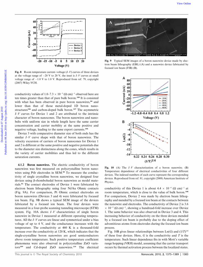
Fig. 8 Room temperature current–voltage (I–V) curves of three devices
at the voltage range of �20 V to 20 V, the inset is I–V curves at small
voltage range of �1.0 V to 1.0 V. Reproduced from ref. 79, copyright
(2007) Wiley-VCH.
Fig. 9 Typical SEM images of a boron nanowire device made by elec-
tron beam lithography (EBL) (A) and a nanowire device fabricated by
focused ion beam (FIB) (B).
Fig. 10 (A) The I–V characterization of a boron nanowire. (B)
Temperature dependence of electrical conductivities of four different
devices. The indexed numbers of each curve represent the corresponding
devices. Reproduced from ref. 81, copyright (2008) American Institute of
Physics.
Dow
nloa
ded
on 0
7 A
ugus
t 201
0Pu
blis
hed
on 0
8 Ju
ne 2
010
on h
ttp://
pubs
.rsc
.org
| do
i:10.
1039
/C0N
R00
051E
View Online
conductivity values of 1.0–7.3 � 10�5 (U cm)�1 observed here are
ten times greater than that of pure bulk boron.108 It is consisted
with what has been observed in pure boron nanowires,84 and
lower than that of those metal-doped 1D boron nano-
structures106 and carbon-doped bulk boron.107 The asymmetric
I–V curves for Device 1 and 2 are attributed to the intrinsic
character of boron nanocones. The boron nanowires and nano-
belts with uniform size in whole length have the same carrier
concentration and carrier mobility at the same positive and
negative voltage, leading to the same export currents.106
Device 3 with comparative diameter size of both ends has the
similar I–V curve shape with that of boron nanowires. The
velocity excursion of carriers of boron nanocones for Device 1
and 2 is different at the same positive and negative potentials due
to the diameter size distinctness along the cones, which results in
the variety of carrier mobilities and thus led to the different
saturation currents.
4.1.2 Boron nanowires. The electric conductivity of boron
nanowires was first measured on polycrystalline boron nano-
wires using PtIr electrodes in SEM.84 To measure the conduc-
tivity of single crystalline boron nanowires, we designed four
devices using b-rhombohedal boron nanowires as model mate-
rials.81 The contact electrodes of Device 1 were fabricated by
electron beam lithography using four Ni/Au Ohmic contacts
(Fig. 9A). For comparison, Pt Ohmic contact electrodes on
boron nanowires (Devices 3 and 4) were fabricated by focused
ion beam. Fig. 9B shows a typical SEM image of the devices
fabricated by a focused ion beam. The four devices were
measured in a four-probe scanning tunneling microscope (STM)
system. Fig. 10A shows I–V characteristics of single boron
nanowire in Device 1 measured at different operating tempera-
tures. All the I–V curves are linear and symmetrical under a bias
voltage of up to 4 V, and the conductance increases with the
temperature. The conductivity at 460 K is a thousand-fold
increase over the conductivity at 120 K, which indicates that the
single-crystalline boron nanowires are good semiconductors
above room temperature. Such positive temperature coefficient
phenomena were also observed in polycrystalline ZnO varis-
tors109 and Cd-doped ZnO nanowires.110 The electrical
This journal is ª The Royal Society of Chemistry 2010
conductivity of this Device 1 is about 4.4 � 10�4 (U cm)�1 at
room temperature, which is close to the value of bulk boron.108
For comparison, Device 2 was made by electron beam lithog-
raphy and mended by a focused ion beam at the contacts between
the nanowire and electrodes. The conductivity of Device 2 is 3.6
� 10�2 (U cm)�1, showing a hundread-fold increase over Device
1. The same behavior was also observed in Device 3 and 4. This
increasing behavior of conductivity on the three devices mended
by a focused ion beam is probably due to the doping effect of
adventitious atoms from electrodes during the focused ion beam
process.
Fig. 10B gives linear relationships between Ln(G) and (1/T)1/4
of these four devices. Here, G is the conductivity and T is the
temperature. Such linear dependence fits in with Mott’s variable
range hopping (VRH) model, assuming that the carrier transport
occurs by thermal activation process between the localized states.
Nanoscale, 2010, 2, 1375–1389 | 1383
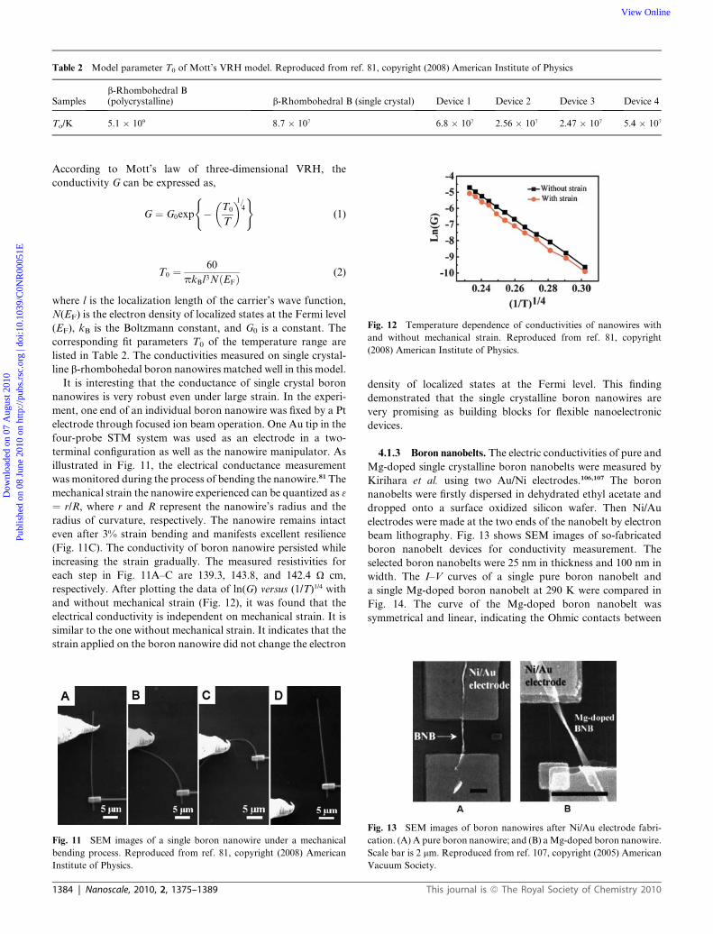
Table 2 Model parameter T0 of Mott’s VRH model. Reproduced from ref. 81, copyright (2008) American Institute of Physics
Samplesb-Rhombohedral B(polycrystalline) b-Rhombohedral B (single crystal) Device 1 Device 2 Device 3 Device 4
To/K 5.1 � 109 8.7 � 107 6.8 � 107 2.56 � 107 2.47 � 107 5.4 � 107
Fig. 12 Temperature dependence of conductivities of nanowires with
and without mechanical strain. Reproduced from ref. 81, copyright
(2008) American Institute of Physics.
Dow
nloa
ded
on 0
7 A
ugus
t 201
0Pu
blis
hed
on 0
8 Ju
ne 2
010
on h
ttp://
pubs
.rsc
.org
| do
i:10.
1039
/C0N
R00
051E
View Online
According to Mott’s law of three-dimensional VRH, the
conductivity G can be expressed as,
G ¼ G0exp
(��
T0
T
�1=4
)(1)
T0 ¼60
pkBl3NðEFÞ(2)
where l is the localization length of the carrier’s wave function,
N(EF) is the electron density of localized states at the Fermi level
(EF), kB is the Boltzmann constant, and G0 is a constant. The
corresponding fit parameters T0 of the temperature range are
listed in Table 2. The conductivities measured on single crystal-
line b-rhombohedal boron nanowires matched well in this model.
It is interesting that the conductance of single crystal boron
nanowires is very robust even under large strain. In the experi-
ment, one end of an individual boron nanowire was fixed by a Pt
electrode through focused ion beam operation. One Au tip in the
four-probe STM system was used as an electrode in a two-
terminal configuration as well as the nanowire manipulator. As
illustrated in Fig. 11, the electrical conductance measurement
was monitored during the process of bending the nanowire.81 The
mechanical strain the nanowire experienced can be quantized as 3
¼ r/R, where r and R represent the nanowire’s radius and the
radius of curvature, respectively. The nanowire remains intact
even after 3% strain bending and manifests excellent resilience
(Fig. 11C). The conductivity of boron nanowire persisted while
increasing the strain gradually. The measured resistivities for
each step in Fig. 11A–C are 139.3, 143.8, and 142.4 U cm,
respectively. After plotting the data of ln(G) versus (1/T)1/4 with
and without mechanical strain (Fig. 12), it was found that the
electrical conductivity is independent on mechanical strain. It is
similar to the one without mechanical strain. It indicates that the
strain applied on the boron nanowire did not change the electron
Fig. 11 SEM images of a single boron nanowire under a mechanical
bending process. Reproduced from ref. 81, copyright (2008) American
Institute of Physics.
1384 | Nanoscale, 2010, 2, 1375–1389
density of localized states at the Fermi level. This finding
demonstrated that the single crystalline boron nanowires are
very promising as building blocks for flexible nanoelectronic
devices.
4.1.3 Boron nanobelts. The electric conductivities of pure and
Mg-doped single crystalline boron nanobelts were measured by
Kirihara et al. using two Au/Ni electrodes.106,107 The boron
nanobelts were firstly dispersed in dehydrated ethyl acetate and
dropped onto a surface oxidized silicon wafer. Then Ni/Au
electrodes were made at the two ends of the nanobelt by electron
beam lithography. Fig. 13 shows SEM images of so-fabricated
boron nanobelt devices for conductivity measurement. The
selected boron nanobelts were 25 nm in thickness and 100 nm in
width. The I–V curves of a single pure boron nanobelt and
a single Mg-doped boron nanobelt at 290 K were compared in
Fig. 14. The curve of the Mg-doped boron nanobelt was
symmetrical and linear, indicating the Ohmic contacts between
Fig. 13 SEM images of boron nanowires after Ni/Au electrode fabri-
cation. (A) A pure boron nanowire; and (B) a Mg-doped boron nanowire.
Scale bar is 2 mm. Reproduced from ref. 107, copyright (2005) American
Vacuum Society.
This journal is ª The Royal Society of Chemistry 2010

Fig. 14 I–V characteristics of a pure boron nanobelt and a Mg-doped
boron nanobelt measured at 290 K. Reproduced from ref. 107, copyright
(2005) American Vacuum Society.
Dow
nloa
ded
on 0
7 A
ugus
t 201
0Pu
blis
hed
on 0
8 Ju
ne 2
010
on h
ttp://
pubs
.rsc
.org
| do
i:10.
1039
/C0N
R00
051E
View Online
the nanobelt and the electrodes. The slope of Mg-doped I–V
curve was much steeper than that of the pure boron nanobelt
after Mg vapor diffusion. The measured electric conductivities at
290 K for pure boron nanobelts and Mg-doped ones were 2.2 �10�3 (U cm)�1 and 2.8 � 10�1 (U cm)�1, respectively. The doped
nanobelt showed a hundred-fold increase in electric conductivity
over the pure one. The temperature dependence of conductivities
of the pure and doped boron nanobelts was also studied at the
same time by Kirihara et al.107 They found that both pure and
doped nanobelts exhibited semiconductor behavior. Their slopes
of I–V curves increased with increasing temperature. A very
small current was recorded at 34 K for the Mg-doped boron
nanobelt and this low temperature is lower than the transition
temperature of superconductor MgB2.111 It indicates that there
was no MgB2 formed in the boron nanobelt and Mg was indeed
doped in the boron. In addition, the temperature induced slope
change of I–V curves of the Mg-doped nanobelt was slower than
that of the pure boron nanobelt. This feature indicates that
temperature coefficient of electric conductance was not signifi-
cant in the doped boron nanobelt. The conductivity increase
observed on the Mg-doped boron nanobelt was ascribed to the
occupation of the interstitial sites by Mg atoms or trace Si atoms,
which donated electrons to the densely distributed IALs in a rigid
band scheme and thus resulted in a high value of N(EF).107
Fig. 15 Field-emission J–V curve of boron nanocones and corre-
sponding F–N plot, which is divided into three regions (inset). Repro-
duced from ref. 79, copyright (2007) Wiley-VCH.
4.2 Field emssion
Metal or semiconductor 1D nanostructures such as nanotubes
and nanowires have been well accepted as ideal field emission
electron sources for emitting electrons at low electric field due to
their nanoscale and special geometry (high aspect ratio and lower
curvature radius).43,112,113 A good emitter material for field
emission requires not only a low turn-on voltage, but also a high
durable emission current. It needs some properties, such as small
electron affinity, low work function, high aspect ratio, high
thermal stability and better mechanical strength at high
temperature. In the past decade, a lot of materials including
Spindt-tip arrays,114 low electron affinity III–V nitride nano-
cones/nanowires,115,116 diamond films,117 transition metal oxide
nanowires,118–121 and carbon nanotubes122–124 have been system-
ically studied as field emitters. Among these nanostructures,
This journal is ª The Royal Society of Chemistry 2010
carbon nanotubes were well-recognized as one of best field
emission materials. However, due to their poor emission stability
and low melting point, carbon nanotubes are limited in building
field emission devices. This section reviews the field emission
properties of single crystalline boron 1D nanostructures.
Compared to other materials, the nature of boron offers its 1D
nanostructures many advantages, such as a high melting point
ensuring long-term stability, low-electron-affinity-induced large-
field emission current density, and strong mechanical strength,
resulting in high mechanical performance.
4.2.1 Boron nanocones. The field emission properties of
boron nanocones were studied using a boron nanocone thin film
on silicon substrate. Fig. 15 shows its current density versus the
electric field J–V characteristics.79 The turn-on electric field and
the threshold electric field were defined as 10 mA cm�2 and 1 mA
cm�2, respectively. For boron nanocones, low turn-on and
threshold electric fields were found at 3.5 and 5.3 V mm�1,
respectively. The emission current density was increased to
25 mA cm�2, with no saturation tendency as the electric field was
increased to 12 V mm�1. The J–V relationship was analyzed by
the Fowler–Nordheim (F–N) function and the corresponding F–
N plot is shown in the inset of Fig. 15. It exhibits a nonlinear
behavior in the measurement range of 0.07–0.30 mm V�1. The
ln(J/E2) versus 1/E curve could be approximately divided into
three regions for these boron nanocones. Region 1 refers to a low
electric field, where field emission mainly depends on the surface
states. With increasing the electric field, the surface potential
barrier decreases and the current increases rapidly. In Region 3,
the field penetration breaks down the surface potential barrier to
dominante the field emission. Region 2 is a transition state
between Region 1 and 3. It shows a competition between the
surface states and the field penetration. In addition, high stability
at a high emitting current was also found in these boron nano-
cones. An average emission current density of 25 mA cm�2 was
set at a constant electric field of 12 V mm�1 and its fluctuations
were recorded over 12 h. The fluctuation of the current density
was less than �3% and no remarkable degradation was found
during the measurement.
Nanoscale, 2010, 2, 1375–1389 | 1385

Fig. 17 (A) The current-electric field (I–E) curves of individual boron
nanowires: a–c refer to the three different boron nanowires. (B) The
corresponding current–voltage (I–V) curves of these three individual
boron nanowires (a–c) in FE measurements. Reproduced from ref. 80,
copyright (2005) Wiley-VCH.
Dow
nloa
ded
on 0
7 A
ugus
t 201
0Pu
blis
hed
on 0
8 Ju
ne 2
010
on h
ttp://
pubs
.rsc
.org
| do
i:10.
1039
/C0N
R00
051E
View Online
4.2.2 Individual boron nanowire. We first measured the field
emission properties of an individual boron nanowire using
a modified high vacuum SEM system.80 As illustrated in Fig. 16,
the tungsten probe was moved to contact an individual boron
nanowire and the resistance along the nanowire was recorded by
a pico-amperemeter. The detected voltage on the probe was�5 V
at this step to ensure the alignment as well as the Ohmic contact
between the probe and the nanowire. The tungsten probe was
then retracted to a distance from the boron nanowire by a step-
ped motor. As the probe left the boron nanowire, the voltage
from the pico-amperemeter returned to zero. The field emission
current was recorded as a function of the applied voltage up to
200 V in steps of 0.5–1 V. By measuring many nanowires indi-
vidually, there were three representative curves of current versus
electric field (I–E) as shown in Fig. 17A. A stable field emission
current of 1mA was reached under the applied electric field
between 59 and 74 V mm�1. The calculation based on this result
gave a maximum emission current density of 2 � 105–4 � 105 A
cm�2, which indicates boron nanowires may be a promising
candidate as high-brightness point electron sources.
It is noticed that these three representative field emission
behaviors exhibited slight differences. Nanowire a showed the
best behavior although there was no remarkbale morphology
difference among the three nanowires. To explore the details of
field emission behavior, the conductivity of these three typical
nanowires was also measured and plotted in Fig. 17B. Through
this measurement, it was found that the three nanowires process
different electrical conductivities. Nanowire a and c showed the
highest (8 � 10�3 (U cm)�1) and the lowest (3.2 � 10�3 (U cm)�1)
conductivities, respectively. It is probably the difference in
conductivity that results in the difference in field emission
behavior. These results suggested that the field emission perfor-
mance of an individual boron nanowire seems proportional to its
electrical conductance. The measured field emission featured
a behavior up to 4 mA without breaking down, which is very
Fig. 16 SEM images of the single boron nanowire during FE
measurements. SEM images of the W probe and the single nanowire (A)
before and (B) during the measurement. Reproduced from ref. 80,
copyright (2005) Wiley-VCH.
1386 | Nanoscale, 2010, 2, 1375–1389
encouraging compared to the best results obtained from other
nanowires.125–127
4.2.3 Boron nanowire arrays. The successful syntheis of
aligned boron nanowires in a large scale provided us the
opportunity to measure the field emission behavior of boron
nanowire arrays.80 Fig. 18A shows the field emission curve of
current density versus electric field (J–E) from large-area boron
nanowire arrays. The turn-on electric field (Eon) and the
threshold electric field (Ethres) of the nanowire arrays are 5.1 V
mm�1 (J ¼ 10 mA cm�2) and 11.5 V mm�1 (J ¼ 1 mA cm�2),
respectively. Increasing the electric field to 17.8 Vmm�1 resulted in
a higher current density of 8.1 mA cm�2 without the saturation
tendency. The Ethres value of the boron nanowire arrays is higher
than that of carbon nanotubes (1.6 V mm�1)128 and tungsten oxide
nanowires (6.2 V mm�1).129 Since nanowire arrays in a very high
density are often harmful to field electron emission due to
screening effects,130,131 attempts were made to control the density
of these vertical boron nanowire arrays to fit in with the opti-
mized theoretical values.132,133 Fig. 18B is the FN plot of the
arrays of aligned boron nanowires. The FN plot is almost linear,
agreeing well with the FN theory. However, the field emission
behavior of the boron nanowire arrays at high current density is
different from that of an individual boron nanowire. This is
probably because the proportion of the thermal electron current
for arrays in the measured field-emission current at high current
density is too small to contribute to the FN plot. Since the field
emission behavior of boron nanowire arrays was studied on
a high density nanowire film, it partially concealed the true field
emission properties of boron nanowires and thus a clear under-
standing on its field emission mechanism is still desirable.
This journal is ª The Royal Society of Chemistry 2010

Fig. 18 (A) The J–E field-emission curve of a large-area film of vertically
aligned boron nanowires. (B) FN plot of this sample. Reproduced from
ref. 80, copyright (2008) Wiley-VCH.
Dow
nloa
ded
on 0
7 A
ugus
t 201
0Pu
blis
hed
on 0
8 Ju
ne 2
010
on h
ttp://
pubs
.rsc
.org
| do
i:10.
1039
/C0N
R00
051E
View Online
4.2.4 Patterned boron nanowires. Since a high density of
nanowire arrays may lead to screening effects during field emis-
sion, patterned field emission materials with a controlled interval
distance on a substrate have attracted great attention in the
fabrication of display units. As presented in the method section,
we have successfully fabricated patterned boron nanowires using
a catalyst patterned silicon substrate.82 The distance between
these boron nanowire patterns were about 20–30 mm and each
pattern was 10–15 mm in diameter. In the measurement, the
vacuum gap between the boron nanowires and Mo tip was 300
mm under a pressure of 2 � 10�6 Pa. Fig. 19 shows the field
emission curve of current density versus electric field (J–E) from
the patterned boron nanowires. The turn-on field is 15 V mm�1
(defined as the applied field of 10 mm cm�1) and the apparent
threshold field is 24 V mm�1 (defined as the applied field of 1 mA
cm�2). The measured turn-on field is higher than that of boron
nanocones, but still lower than other field emission materials,
Fig. 19 Typical field emission characteristics of the patterned boron
nanowires. Reproduced from ref. 82, copyright (2009) American Institute
of Physics.
This journal is ª The Royal Society of Chemistry 2010
such as AlN nanocones134 and nanowires.135–137 This moderate
turn-on field might be ascribed to the fact that the distance
between each pattern is larger than the distance for the most
effective electron emission. It has been well-accepted that the
most effective nanowire emitters usually have their ratio of the
interval distance to the nanowire length close to 1. In this case,
the distance between each pattern is 20–30 mm and the length of
boron nanowires is about 5 mm, giving a ratio of 4–6. The high
density of boron nanowires on each pattern probably also
resulted in a screening effect. In addition, the random orientation
of the nanowires also partially contributed to the moderate turn-
on field.82
Conclusions and outlook
Recent advances in the dynamic area of boron nanostructures
have been drafted in this review paper. Recently, various 1D
boron nanomaterials, such as nanowires, nanobelts, nanocones
and nanotubes have been successfully synthesized by chemical
and physical methods. We classified these methods into three
categories: 1) chemical vapor deposition (CVD) with gas or solid
precursors; 2) magnetron sputtering; and 3) laser ablation.
Several technical approaches for fabricating high density boron
1D nanostructure arrays and patterned nanostructures were also
discussed. Although significant progress has been made on
controlled growth of 1D boron nanostructures, a breakthrough
in terms of highly ordered arrays, large scale synthesis, patterned
growth, morphology control as well as simplifying current
recipes is still highly desired. In particular, the controlled
synthesis of boron nanotubes currently is a focus area to be
developed since the theoretical studies have predicted a high
electric conductivity of boron nanotubes, which are promising to
exhibit even higher electric conductivity than carbon nano-
tubes.56,58 To date, only one attempt was successful on the
synthesis of boron nanotubes by employing Mg-MCM-41 as
template99 and the progress on high quality, large scale or highly
crystalline boron nanotubes as well as the transport measure-
ments on these novel structures remained blank in this field.
More efforts from the experimental community are still required
to develop new methods not only to synthesis novel nano-
structures (such as nanotubes and fullerenes) but also to run
measurements on the conductivity of these nanostructures. To
verify these theoretical predictions of boron nanostructures
experimentally is not only fundamentally interesting, but also
appealing for the discovery of new generation nanodevices.
The two main physical properties of 1D boron nanostructures
are electronic transport and field emission, which are quite
interesting as they give 1D boron nanostructures great potential
for field emission, flexible displays, superconductors, energy
storage, and nanoelectronic devices. However, like most popular
1D nanomaterials, there are still many key scientific problems to
be understood for their true application. One aspect is the rela-
tionship between the transport properties and crystal structures
of boron. Boron has several different crystal structures. It is
important to study the transport properties of boron nano-
structures with different crystal structures. Moreover, more
effort should be devoted to understand the transport mechanism
by varying the measurement conditions, such as temperature,
strain, and doping. For field emission applications, more
Nanoscale, 2010, 2, 1375–1389 | 1387

Dow
nloa
ded
on 0
7 A
ugus
t 201
0Pu
blis
hed
on 0
8 Ju
ne 2
010
on h
ttp://
pubs
.rsc
.org
| do
i:10.
1039
/C0N
R00
051E
View Online
attention may be paid to both synthesis techniques and property
measurements. Boron nanostructures with uniform size, proper
density, and/or a controlled interval distance are highly essential
to enhance the properties of field emission. In addition, to realize
flexible displays, flexible and conductive substrates for growing
boron nanostructures are also highly desired.
There are almost unlimited research opportunities that are
being and will be explored by researchers in this dynamic area.
By understanding these scientific and technical issues, we believe
that 1D boron nanostructures will continue to give exciting
results toward their application.
Acknowledgements
The work is supported by National High Technology Program of
China (863 Program, Grant No. 2007AA03Z305), National
Basic Research Program of China (973 Program, Grant No.
2007CB935500) and National Natural Science Foundation of
China (Grant No. 50872147, U0734003).
Notes and references
1 Y. Xia, P. Yang, Y. Sun, Y. Wu, B. Mayers, B. Gates, Y. Yin,F. Kim and H. Yan, Adv. Mater., 2003, 15, 353.
2 P. Alivisatos, Pure Appl. Chem., 2000, 72, 3.3 M. Nirmal and L. Brus, Acc. Chem. Res., 1999, 32, 407.4 H. Pettersson, L. Baath, N. Carlsson, W. Seifert and L. Samuelson,
Appl. Phys. Lett., 2001, 79, 78.5 V. I. Klimov, A. A. Mikhailovsky, S. Xu, A. Malko,
J. A. Hollingsworth, C. A. Leatherdale, H. J. Eisler andM. G. Bawendi, Science, 2000, 314, 290.
6 J. Phillips, J. Appl. Phys., 2002, 91, 4590.7 D. L. Klein, R. Roth, A. K. L. Lim, A. P. Alivisatos and
P. L. McEuen, Nature, 1997, 389, 699.8 H. Sakaki, Jpn. J. Appl. Phys., 1980, 19, L735.9 Z. G. Wu, J. B. Neaton and J. C. Grossman, Phys. Rev. Lett., 2008,
100, 246804.10 G. Hodes, Adv. Mater., 2007, 19, 639.11 Q. Zhu, K. F. Karlsson, E. Pelucchi and E. Kapon, Nano Lett., 2007,
7, 2227.12 Z. (J. ) Xu, M. Lu, X. Guo and H. Lin, J. Mol. Catal. A: Chem.,
2005, 226, 123.13 G. Che, B. B. Lakshmi, C. R. Martin and E. R. Fisher, Langmuir,
1999, 15, 750.14 N. Wang, Y. Cai and R. Q. Zhang, Mater. Sci. Eng., R, 2008, 60, 1–
51.15 C. M. Lieber and Z. L. Wang, MRS Bull., 2007, 32, 99–108.16 F. Liu, P. J. Cao, H. R. Zhang, C. M. Shen, J. Q. Li and H.-J. Gao, J.
Cryst. Growth, 2005, 274, 126–131.17 Z. W. Pan, Z. R. Dai and Z. L. Wang, Science, 2001, 291, 1947.18 C. Li, D. H. Zhang, S. Han, X. L. Liu, T. Tang and C. W. Zhou, Adv.
Mater., 2003, 15, 143.19 Z. R. Dai, J. L. Gole, J. D. Stout and Z. L. Wang, J. Phys. Chem. B,
2002, 106, 1274.20 M. S. Dresselhaus, G. Dresselhaus, and P. Avouris, Carbon
Nanotubes: Synthesis, Structure, and Application, Springer, NewYork, 2001.
21 T. Guo, P. Nokolaev, A. Thess, D. T. Colbert and R. E. Smalley,Chem. Phys. Lett., 1995, 243, 49.
22 S. S. Fan, M. G. Chapline, N. R. Franklin, T. W. Tombler,A. M. Cassell and H. J. Dai, Science, 1999, 283, 512.
23 A. M. Morales and C. M. Lieber, Science, 1998, 279, 208.24 D. Wang and H. Dai, Appl. Phys. A: Mater. Sci. Process., 2006, 85,
217.25 S. A. Dayeh, E. T. Yu and D. L. Wang, J. Phys. Chem. C, 2007, 111,
13331.26 C. Liu, Z. Hu, Q. Wu, X. Z. Wang, Y. Chen, H. Sang, J. M. Zhu,
S. Z. Deng and N. S. Xu, J. Am. Chem. Soc., 2005, 127, 1318.
1388 | Nanoscale, 2010, 2, 1375–1389
27 N. G. Chopra, R. J. Luyken, K. Cherrey, V. H. Crespi, M. L. Cohen,S. G. Louie and A. Zettl, Science, 1995, 269, 966.
28 D. V. Talapin, E. V. Shevchenko, C. B. Murray, A. Kornowski,S. F€orster and H. Weller, J. Am. Chem. Soc., 2004, 126, 12984.
29 C. M. Shen, X. G. Zhang and H. L. Li, Mater. Sci. Eng., A, 2001,303, 19.
30 Y. Jiang, X. M. Meng, W. C. Yiu, J. Liu, J. X. Ding, C. S. Lee andS. T. Lee, J. Phys. Chem. B, 2004, 108, 2784.
31 R. H. Baughman, A. A. Zakhidov and W. A. de Heer, Science, 2002,297, 787.
32 D. R. Kauffman and A. Star, Small, 2007, 3, 1324.33 Z. Y. Fan, D. W. Wang, P. C. Chang, W. Y. Tseng and J. G. Lu,
Appl. Phys. Lett., 2004, 85, 5923.34 X. D. Wang, J. H. Song, J. Liu and Z. L. Wang, Science, 2007, 316,
102.35 X. F. Duan, Y. Huang, Y. Cui, J. F. Wang and C. M. Lieber, Nature,
2001, 409, 66–69.36 J. M. Bao, M. A. Zimmler and F. Capasso, Nano Lett., 2006, 6,
1719.37 F. Qian, S. Grade�cak, Y. Li, C. Y. Wen and C. M. Lieber, Nano
Lett., 2005, 5, 2287.38 A. M. Rao, X. H. Ji and Terry M. Tritt, MRS Bull., 2006, 31, 218.39 A. I. Hochbaum, R. K. Chen, R. D. Delgado, W. J. Liang,
E. C. Garnett, M. Najarian, A. Majumdar and P. D. Yang,Nature, 2008, 451, 163.
40 A. I. Boukai, Y. Bunimovich, J. Tahir-Kheli, J. K. Yu,W. A. Goddard and J. R. Heath, Nature, 2008, 451, 168.
41 Y. Huang and C. M. Lieber, Pure Appl. Chem., 2004, 76, 2051.42 W. A. de Heer, A. Chatelain and D. Ugarte, Science, 1995, 270, 1179.43 W. I. Milne, K. B. K. Teo, G. A. J. Amaratunga, P. Legagneux,
L. Gangloff, J.-P. Schnell, V. Semet, V. T. Binh and O. Groening,J. Mater. Chem., 2004, 14, 933.
44 N. S. Xu and S. Ejaz, Mater. Sci. Eng., R, 2005, 48, 47.45 J. Zhou, L. Gong, S. Z. Deng, J. Chen, J. C. She, N. S. Xu, R. Yang
and Z. Wang, Appl. Phys. Lett., 2005, 87, 223108.46 Z. Y. Fan, D. W. Wang, P. C. Chang, W. Y. Tseng and J. G. Lu,
Appl. Phys. Lett., 2004, 85, 5923.47 Q. Wan and T. H. Wang, Chem. Commun., 2005, 3841.48 X. F. Chu, C. H. Wang, D. L. Jiang and C. M. Zheng, Chem. Phys.
Lett., 2004, 399, 461.49 N. N. Greenwood and A. Earnshaw, Chemistry of the Elements,
Butterworth-Heinemann, Oxford, 1998.50 G. V. Tsagareishvili and F. N. Tavadze, Prog. Cryst. Growth
Charact. Mater., 1988, 16, 341.51 D. Emin, Phys. Today, 1987, 40, 55.52 G. K. Gaule, Boron: Preparation, Properties, and Application,
Plenum, New York, 1965.53 D. G. Hinks, H. Claus and J. D. Jorgensen, Nature, 2001, 411, 457.54 A. Ulas, K. K. Kuo and C. Gotzmer, Combust. Flame, 2001, 127,
1935.55 I. Boustani and A. Quandt, Europhys. Lett., 1997, 39, 527.56 I. Boustani, A. Quandt, E. Hern�andez and A. Rubio, J. Chem. Phys.,
1999, 110, 3176.57 K. C. Lau, R. Pandey, R. Pati and S. P. Karna, Appl. Phys. Lett.,
2006, 88, 212111.58 J. Kunstmann and A. Quandt, Chem. Phys. Lett., 2005, 402, 21.59 I. Boustani, Surf. Sci., 1997, 370, 355.60 I. Boustani, Phys. Rev. B: Condens. Matter, 1997, 55, 16426.61 S. Chacko, D. G. Kanhere and I. Boustani, Phys. Rev. B: Condens.
Matter Mater. Phys., 2003, 68, 035414.62 M. Fujimori, T. Nakata, T. Nakayama, E. Nishibori, K. Kimura,
M. Takata and M. Sakata, Phys. Rev. Lett., 1999, 82, 4452.63 L. Pauling, Nature of the Chemical Bond, Cornell University Press,
Ithaca, 1960.64 H. J. Zhai, B. Kiran, J. Li and L. S. Wang, Nat. Mater., 2003, 2, 827.65 A. Quandt and I. Boustani, ChemPhysChem, 2005, 6, 2001.66 A. Gindulyt_e, W. N. Lipscomb and L. Massa, Inorg. Chem., 1998,
37, 6544.67 H. Tang and S. Ismail-Beigi, Phys. Rev. Lett., 2007, 99, 115501.68 J. Miller, Phys. Today, 2007, 20.69 X. B. Yang, Y. Ding and J. Ni, Phys. Rev. B: Condens. Matter
Mater. Phys., 2008, 77, 041402.70 Y. Y. Wu, B. Messer and P. D. Yang, Adv. Mater., 2001, 13, 1487.71 S. H. Yun, J. Z. Wu, A. Dias, X. Gao and U. O. Karlsson, Appl.
Phys. Lett., 2005, 87, 113109.
This journal is ª The Royal Society of Chemistry 2010

Dow
nloa
ded
on 0
7 A
ugus
t 201
0Pu
blis
hed
on 0
8 Ju
ne 2
010
on h
ttp://
pubs
.rsc
.org
| do
i:10.
1039
/C0N
R00
051E
View Online
72 S. H. Yun, J. Z. Wu, A. Dibos, X. D. Zou and U. O. Karlsson, NanoLett., 2006, 6, 385.
73 P. J. Cao, H. W. Liu, F. Shen, Y. G. Wang and H.-J. Gao, J. Mater.Res., 2003, 18, 1686.
74 F. Liu, P. J. Cao, H. R. Zhang, J. Q. Li and H.-J. Gao,Nanotechnology, 2004, 15, 949.
75 F. Liu, P. J. Cao, H. R. Zhang, C. M. Shen, J. Q. Li and H.-J. Gao, J.Cryst. Growth, 2005, 274, 126.
76 F. Liu, P. J. Cao, H. R. Zhang, J. F. Tian, C. W. Xiao, C. M. Shen,J. Q. Li and H.-J. Gao, Adv. Mater., 2005, 17, 1893.
77 J. F. Tian, F. Liu, C. M. Shen, L. H. Bao, X. J. Wang, D. T. Liu,H. Li, X. J. Huang, L. Q. Chen and H.-J. Gao, J. Mater. Res.,2007, 22, 1921.
78 J. F. Tian, X. J. Wang, L. H. Bao, C. Hui, F. Liu, T. Z. Yang,C. M. Shen and H.-J. Gao, Cryst. Growth Des., 2008, 8, 3160.
79 X. J. Wang, J. F. Tian, T. Z. Yang, L. H. Bao, C. Hui, F. Liu,C. M. Shen, N. S. Xu and H.-J. Gao, Adv. Mater., 2007, 19, 4480.
80 F. Liu, J. F. Tian, L. H. Bao, T. Z. Yang, C. M. Shen, X. Y. Lai,Z. M. Xiao, W. G. Xie, S. Z. Deng, J. Chen, J. C. She, N. S. Xuand H.-J. Gao, Adv. Mater., 2008, 20, 2609.
81 J. F. Tian, J. M. Cai, C. Hui, C. D. Zhang, L. H. Bao, M. Gao,C. M. Shen and H.-J. Gao, Appl. Phys. Lett., 2008, 93, 122105.
82 J. F. Tian, C. Hui, L. H. Bao, C. Li, Y. Tian, H. Ding, C. M. Shenand H.-J. Gao, Appl. Phys. Lett., 2009, 94, 083101.
83 T. Z. Yang, C. M. Shen, Z. A. Li, H. R. Zhang, C. W. Xiao,S. T. Chen, Z. C. Xu, D. X. Shi, J. Q. Li and H.-J. Gao, J. Phys.Chem. B, 2005, 109, 23233.
84 C. J. Otten, O. R. Loune, M. F. Yu, J. M. Cowley, M. J. Dyer,R. S. Ruoff and W. E. Buhro, J. Am. Chem. Soc., 2002, 124, 4564.
85 Q. Yang, J. Sha, J. Xu, Y. J. Ji, X. Y. Ma, J. J. Niu, H. Q. Hua andD. R. Yang, Chem. Phys. Lett., 2003, 379, 87.
86 T. T. Xu, J. G. Zheng, N. Q. Wu, A. W. Nicholls, J. R. Roth,D. A. Dikin and R. S. Ruoff, Nano Lett., 2004, 4, 963.
87 L. Guo, R. N. Singh and H. -J. Kleebe, Chem. Vap. Deposition, 2006,12, 448.
88 L. M. Cao, Z. Zhang, L. L. Sun, M. He, Y. Q. Wang, Y. C. Li,X. Y. Zhang, G. Li, J. Zhang and W. K. Wang, Adv. Mater.,2001, 13, 1701; Y. Q. Wang, X. F. Duan, L. M. Cao andW. K. Wang, Chem. Phys. Lett., 2002, 359, 273.
89 L. M. Cao, K. Hahn, Y. Q. Wang, C. Scheu, Z. Zhang, C. X. Gao,Y. C. Li, X. Y. Zhang, L. L. Sun and W. K. Wang, Adv. Mater.,2002, 14, 1294.
90 Y. Q. Wang, L. M. Cao and X. F. duan, Chem. Phys. Lett., 2003,367, 495–499.
91 L. M. Cao, K. Hahn, M. Ruhle, C. Scheu, Y. Q. Wang, Z. Zhang,C. X. Gao, Y. C. Li, X. Y. Zhang, M. He, L. L. Sun andW. K. Wang, Appl. Phys. Lett., 2002, 80, 4226.
92 Y. P. Gao, Z. Xu and R. P. Liu, Mater. Sci. Eng., A, 2006, 434, 53.93 Y. J. Zhang, H. Ago, M. Yumura, T. Komatsu, S. Ohshima,
K. Uchida and S. Iijima, Chem. Commun., 2002, 2806.94 Z. K. Wang, Y. Shimizu, T. Sasaki, K. Kawaguchi, K. Kimura and
N. Koshizaki, Chem. Phys. Lett., 2003, 368, 663; Z. Wang, T. Sasaki,Y. Shimizu, K. Kirihara, K. Kawaguchi, K. Kimura andN. Koshizaki, Appl. Phys. A: Mater. Sci. Process., 2004, 79, 891.
95 X. M. Meng, J. Q. Hu, Y. Jiang, C. S. Lee and S. T. Lee, Chem. Phys.Lett., 2003, 370, 825.
96 Y. J. Zhang, H. Ago, M. Yumura, S. Ohshima, K. Uchida,T. Komatsu and S. Iijima, Chem. Phys. Lett., 2004, 385, 177.
97 Y. Q. Wang and X. F. Duan, Appl. Phys. Lett., 2003, 82, 272.98 Q. Yang, J. Sha, L. Wang, Z. Xu, X. Ma, J. Wang and D. Yang, J.
Mater. Sci., 2006, 41, 3547.99 D. Ciuparu, R. F. Klie, Y. Zhu and L. Pfefferle, J. Phys. Chem. B,
2004, 108, 3867.100 S. H. Yun, A. Dibos, J. Z. Wu and D. K. Kim, Appl. Phys. Lett.,
2004, 84, 2892.101 S. M. Sze, Semiconductor Devices: Physics and Technology, Wiley,
New York, 1985.102 W. Menz, J. Mohr and O. Paul, Microsystem Technology, 2nd edn,
Wiley-VCH, Weinheim, 2001.103 M. Geissler and Y. Xia, Adv. Mater., 2004, 16, 1249.
This journal is ª The Royal Society of Chemistry 2010
104 H. He, R. Pandey, I. Boustani and S. P. Karna, J. Phys. Chem. C,2010, 114, 4149.
105 D. W. Wang, J. G. Lu, C. Jones Otten and W. E. Buhro, Appl. Phys.Lett., 2003, 83, 5280.
106 K. Kirihara, Z. Wang, K. Kawaguchi, Y. Shimizu, T. Sasaki,N. Koshizaki, K. Soga and K. Kimura, Appl. Phys. Lett., 2005,86, 212101.
107 K. Kirihara, Z. Wang, K. Kawaguchi, Y. Shimizu, T. Sasaki,N. Koshizaki, H. Hyodo, K. Soga and K. Kimura, J. Vac. Sci.Technol., B, 2005, 23, 2510.
108 K. H. Hellwege, Landolt–Bornstein Numerical Data and FunctionalRelationships, in Science and Technology, Springer, Berlin 1983.
109 D. Femandez-Hevia, J. de Frutos, A. C. Cabalero andJ. F. Fernandez, Appl. Phys. Lett., 2003, 82, 212.
110 Q. H. Li, Q. Wan, Y. G. Wang and T. H. Wang, Appl. Phys. Lett.,2005, 86, 263101.
111 J. Nagamatsu, N. Nakagawa, T. Muranaka, Y. Zenitani andJ. Akimitsu, Nature, 2001, 410, 63.
112 H. J. Dai, Acc. Chem. Res., 2002, 35, 1035.113 X. S. Fang, Y. Bando, U. K. Gautam, C. H. Ye and D. Golberg,
J. Mater. Chem., 2008, 18, 509.114 A. A. Talin, K. A. Dean and J. E. Jaslie, Solid-State Electron., 2001,
45, 963.115 Q. Zhao, J. Xu, X. Y. Xu, Z. Wang and D. P. Yu, Appl. Phys. Lett.,
2004, 85, 5331.116 S. C. Shi, C. F. Chen, St. Chattopadhyay, K. H. Chen and
L. C. Chen, Appl. Phys. Lett., 2005, 87, 073109.117 M. W. Geis, J. C. Twicell, J. Macaulay and K. Okana, Appl. Phys.
Lett., 1995, 67, 1328.118 Y. B. Li, Y. Bando and D. Golberg, Appl. Phys. Lett., 2004, 84,
3603.119 W. Z. Wang, B. Q. Zeng, J. Yang, B. Poudel, J. Y. Huang,
M. J. Naughton and Z. F. Ren, Adv. Mater., 2006, 18, 3275.120 G. C. Yi, C. R. Wang and W. Il Park, Semicond. Sci. Technol., 2005,
20, S22.121 J. Chen, Y. Y. Dai, J. Luo, Z. L. Li, S. Z. Deng, J. C. She and
N. S. Xu, Appl. Phys. Lett., 2007, 90, 253105.122 J. M. Bonard, N. Weiss, H. Kind, T. St€ockli, L. Forr�o, K. Kern and
A. Chatelain, Adv. Mater., 2001, 13, 184.123 S. D. Liang and N. S. Xu, Appl. Phys. Lett., 2003, 83, 1213.124 P. Yaghoobi and A. Nojeh, Mod. Phys. Lett. B, 2007, 21, 1807.125 H. Zhang, J. Tang, Q. Zhang, G. Zhao, G. Yang, J. Zhang, O. Zhou
and L.-C. Qin, Adv. Mater., 2006, 18, 87.126 N. S. Ramgir, I. S. Mulla, K. Vijayamohanan, D. J. Late,
A. B. Bhise, M. A. More and D. S. Joag, Appl. Phys. Lett., 2006,88, 107.
127 Y. Yu, C. H. Jin, R. H. Wang, Q. Chen and L.-M. Peng, J. Phys.Chem. B, 2005, 109, 772.
128 M. Rao, D. Jacques, R. C. Haddon, W. Zhu, C. Bower and S. Jin,Appl. Phys. Lett., 2000, 76, 3813.
129 Y. B. Li, Y. Bando and D. Golberg, Adv. Mater., 2003, 15, 1294.130 J.-M. Bonard, K. A. Dean, B. F. Coll and C. Klinke, Phys. Rev.
Lett., 2002, 89(197), 602.131 L. Nilsson, O. Groening, C. Emmenegger, O. Kuettel, E. Schaller,
L. Schlapbach, H. Kind, J.-M. Bonard and K. Kern, Appl. Phys.Lett., 2000, 76, 2071.
132 J.-M. Bonard, N. Weiss, H. Kind, T. Sto€ockli, L. Forro�o, K. Kernand A. Chatelain, Adv. Mater., 2001, 13, 184.
133 L. Nilsson, O. Groening, P. Groening, O. Kuettel andL. Schlapbach, J. Appl. Phys., 2001, 90, 768.
134 C. Liu, Z. Hu, Q. Wu, X. Z. Wang, Y. Chen, H. Sang, J. M. Zhu,S. Z. Deng and N. S. Xu, J. Am. Chem. Soc., 2005, 127, 1318.
135 K. H. Chen, J. J. Wu, L. C. Chen, C. Y. Wen, P. D. Kichambare,F. G. Tarntair, P. F. Kuo, S. W. Chang and Y. F. Chen, DiamondRelat. Mater., 2000, 9, 124.
136 F. G. Tarntair, C. Y. Wen, L. C. Chen, J. J. Wu, K. H. Chen,P. F. Kuo, S. W. Chang, Y. F. Chen, W. K. Hong andH. C. Cheng, Appl. Phys. Lett., 2000, 76, 2630.
137 K. W. Wong, X. T. Zhou, F. C. K. Au, H. L. Lai, C. S. Lee andS. T. Lee, Appl. Phys. Lett., 1999, 75, 2918.
Nanoscale, 2010, 2, 1375–1389 | 1389