open-access silicon photonics platforms in europe
TRANSCRIPT
IEEE JOURNAL OF SELECTED TOPICS IN QUANTUM ELECTRONICS, VOL. 25, NO. 5, SEPTEMBER/OCTOBER 2019 8200818
Open-Access Silicon Photonics Platforms in EuropeAbdul Rahim , Jeroen Goyvaerts, Bertrand Szelag , Jean-Marc Fedeli , Philippe Absil, Timo Aalto ,
Mikko Harjanne , Callum Littlejohns , Graham Reed, Georg Winzer, Stefan Lischke, Lars Zimmermann,Dieter Knoll, Douwe Geuzebroek , Arne Leinse, Michael Geiselmann, Michael Zervas, Hilde Jans, Andim Stassen,
Carlos Domínguez , Pascual Muñoz , Senior Member, IEEE, David Domenech, Anna Lena Giesecke ,Max C. Lemme , Senior Member, IEEE, and Roel Baets , Fellow, IEEE
(Invited Paper)
Abstract—Offering open-access silicon photonics-based tech-nologies has played a pivotal role in unleashing this technologyfrom research laboratories to industry. Fabless enterprises rely onthe open-access of these technologies for their product develop-ment. In the last decade, a diverse set of open-access technologieswith medium and high technology readiness levels have emerged.This paper provides a review of the open-access silicon and sili-con nitride photonic IC technologies offered by the pilot lines of
Manuscript received January 3, 2019; revised March 18, 2019; accepted April26, 2019. Date of publication May 10, 2019; date of current version June 6, 2019.(Corresponding author: Abdul Rahim.)
A. Rahim, J. Goyvaerts, and R. Baets are with the Photonics Research Group,Department of Information Technology, Ghent University—imec and Center forNano- and Biophotonics, Ghent University, Ghent B-9000, Belgium (e-mail:[email protected]; [email protected]; [email protected]).
B. Szelag and J.-M. Fedeli are with the Commissariat à l’Energie Atom-ique et aux Energie Alternatives, University Grenoble Alpes and CEA, LETI,F-38054, Grenoble Cedex, France (e-mail: [email protected]; [email protected]).
P. Absil, H. Jans, and A. Stassen are with the Imec, 3001 Leuven, Belgium(e-mail: [email protected]; [email protected]; [email protected]).
T. Aalto and M. Harjanne are with VTT, FI-02044 Espoo, Finland (e-mail:[email protected]; [email protected]).
C. Littlejohns and G. Reed are with the Optoelectronics Research Cen-tre, University of Southampton, Southampton SO17 1BJ, U.K. (e-mail:[email protected]; [email protected]).
G. Winzer, S. Lischke, and D. Knoll are with IHP Leibniz-Institut fürinnovative Mikroelektronik, 15236 Frankfurt, Germany (e-mail: [email protected]; [email protected]; [email protected]).
L. Zimmermann is with IHP Leibniz-Institut für innovative Mikroelektronik,15236 Frankfurt, Germany, and also with the Siliziumphotonik, Institut fürHochfrequenz- und Halbleiter - Systemtechnologien, Fakultät IV, 10587 Berlin,Germany (e-mail: [email protected]).
D. Geuzebroek and A. Leinse are with the LioniX International BV,Enschede, The Netherlands (e-mail: [email protected]; [email protected]).
M. Geiselmann and M. Zervas are with LIGENTEC, 1015 Lausanne,Switzerland (e-mail: [email protected]; [email protected]).
C. Domínguez is with the Instituto de Microelectrónica de Barcelona(IMB-CNM, CSIC), 08193 Bellaterra, Spain (e-mail: [email protected]).
P. Muñoz is with the Photonics Research Labs, Universitat Politécnica deValencia, 46021 Valencia, Spain (e-mail: [email protected]).
D. Domenech is with the VLC Photonics S.L., 46021 Valencia, Spain (e-mail:[email protected]).
A. L. Giesecke is with AMO GmbH, 52074 Aachen, Germany (e-mail:[email protected]).
M. C. Lemme is with RWTH Aachen University and AMO GmbH, 52074Aachen, Germany (e-mail: [email protected]).
Color versions of one or more of the figures in this paper are available onlineat http://ieeexplore.ieee.org.
Digital Object Identifier 10.1109/JSTQE.2019.2915949
European research institutes and companies. The paper also high-lights upcoming features of these platforms and discusses how theyaddress the long-term market needs.
Index Terms—Silicon photonics, Silicon-on-Insulator, SiliconNitride, CMOS, foundry, open-access, photonic integrated circuits,photonic manufacturing.
I. INTRODUCTION
THE key asset of silicon photonics stems from its abil-ity to provide compact form-factor, high-performance and
low-cost Photonic Integrated Circuits (PICs) [1], [2]. Siliconphotonics uses high-index contrast material systems for PICmanufacturing to provide dense and large-scale integration ofcomplex photonic functions. Such high-index contrast mate-rials require a manufacturing process that can ensure nm-scale process control to deliver high-performance PICs [3]–[5].This allows silicon photonics to benefit from the existing andwell-established Complementary Metal-Oxide Semiconductor(CMOS) manufacturing technology, which results in the low-cost manufacturing of PICs through economics of scale [7],[9]. The cost-effectiveness of silicon photonics even holds formodest volumes by using the existing CMOS-fabs that are fullyloaded with electronics CMOS manufacturing [6].
The public and private investment in R&D has led to a rapiddevelopment of silicon photonics technologies in the last twodecades. CMOS pilot lines and advanced research institutes[10]–[17] have played a pivotal role by: (a) continuously evolv-ing and maturing the technology platforms to reach a high Tech-nology Readiness Level (TRL);1 and (b) making these platformsaccessible with minimal restriction and at low-cost to third par-ties for validating their design innovations. This open-accessmodel enables an economically viable and low-barrier accessto fabless companies where such companies bank on the off-the-shelf Intellectual Property (IP) and technology processes ofpure-play foundries for PIC prototyping and manufacturing.
The open-access foundry model is one of the success storiesof semiconductor electronics [18]. In Europe, CMOS pilot linesof advanced research institutes imitated this model for siliconphotonics-based technologies. For example, ePIXfab – a joint
1The TRL-level of various open-access silicon photonics platforms discussedin this paper follows the definitions provided in the Appendix.
1077-260X © 2019 IEEE. Personal use is permitted, but republication/redistribution requires IEEE permission.See http://www.ieee.org/publications_standards/publications/rights/index.html for more information.

8200818 IEEE JOURNAL OF SELECTED TOPICS IN QUANTUM ELECTRONICS, VOL. 25, NO. 5, SEPTEMBER/OCTOBER 2019
initiative by imec in Belgium and CEA-LETI in France – hostedfrom Ghent University in Belgium, pioneered open-access sili-con photonics technologies in 2006 [7]. Later on this initiativeexpanded to include other European research institutes [8]2. Fol-lowed by that, similar initiatives such as Optoelectronic SystemsIntegration in Silicon (OpSIS) [19], A*STAR Institute of Micro-electronics (IME) [16] and American Institute for Manufactur-ing Integrated Photonics (AIM Photonics) [13] have emerged tostrengthen the open-access foundry model for silicon photonics.
Open-access silicon photonics technologies are offered in dif-ferent modes of access. The type of access-mode can dependon: (a) the nature of innovation (i-e, academic or industrial) or(b) the phase of the design innovation (i-e, a proof-of-concept,prototyping or scale-up for manufacturing). For example, theMultiproject Wafer (MPW) approach is the mode where a usershares the design area with various other users. The sharing ofthe mask and fabrication cost among these users make MPWan excellent low-cost path for proof-of-concept experiments atacademic or industrial early stage R&D [6], [19], [20]. The plat-forms offered by MPW are versatile to address demands from abroad range of applications. Typically in MPW mode, each usergets a few tens of chips fabricated by using the generic baselinetechnology offered by the fab. On the other hand, through (cus-tomized) dedicated engineering runs an end-user gets the fullreticle on a full lot of wafers (typically 20 to 25 wafers) withthe optional flexibility to have customized processes to meet tar-geted specifications. Though considerably more expensive thanMPW, they provide a large number of chips to determine the ma-turity of the design and fabrication process. As the PIC designmeets the performance specifications, the customer may seekroutes for low-, medium-, or high-volume manufacturing, de-pending on the needs of the application.3 In some cases, CMOSpilot lines provide low- and medium-volume manufacturing ofsilicon PICs, typically up to several hundred wafers per order.With the growing industrial interest in high-volume manufactur-ing of silicon photonics products for telecommunication/data-communication applications, which is the biggest driver for thistechnology since its inception, pure-play fabs have started devel-oping open-access silicon photonics technologies [21]. In cer-tain cases, the CMOS pilot lines and research institutes partnerwith pure-play CMOS fabs for the seamless translation fromprototyping towards high-volume manufacturing [22].
While originally silicon photonics was synonymous for PIC-platforms based on Silicon-on-Insulator (SOI) wafers withwaveguides with a silicon core, the field has diversified to someextent to include other material stacks that can be processedon silicon wafers in a CMOS-environment. Most noteworthyis the emergence of Silicon Nitride (SiN) platforms, in whichthe waveguide core is made of silicon nitride. More generally
2Since 2015, the MPW services offered by ePIXfab have been transferredto Europractice IC Service. ePIXfab represents the European silicon photonicsecosystem and has transformed itself into the European Silicon Photonics Al-liance with the mission to promote silicon photonics science, technology andapplications ([Online]. Available: http://epixfab.eu).
3The definition of manufacturing volume used here for silicon PICs is asfollows: up to 50 wafers per order is termed as low-volume manufacturing,up to 500 wafers per order is termed as medium volume and beyond this isconsidered as high-volume manufacturing.
we see strong interest in heterogeneous platforms in which avariety of materials (III-V semiconductors, LiNbO3, polymersetc) are combined with SOI or SiN either through front-end orthrough backend processes. The key unifying feature of siliconphotonics is the capability to process PICs in a silicon technol-ogy environment on large wafers, typically 200 or 300 mm indiameter.
CMOS pilot lines and research institutes have acted as thegateway for the technological innovation in the field of siliconphotonics. This paper provides a brief description of the variousopen-access technology platforms offered by European siliconphotonics research institutes and companies,4 the routes to ac-cess these technologies and the current status of these technologyplatforms. Each technology platform has features, which makeit unique when compared with the other technologies. This di-versity enables the uptake of silicon photonics technology forvarious emerging applications such as sensing and biophotonics[23], [24], light detection and ranging (LiDAR) for automo-tive industry [25], neuromorphic computing [26]–[28], machinelearning [29], [30], quantum information processing [31], [32]and many more. The paper also highlights upcoming features inthese technology platforms and how they are evolving to addressthe upcoming market needs.
II. SILICON-ON-INSULATOR TECHNOLOGY PLATFORMS
This section mentions the salient features of the open-accessSOI-based technology platforms offered by various Europeanfabs. The described platforms are diverse in terms of TRL rang-ing from 5 and upwards, access mechanism (i-e, directly fromthe fab or through a technology broker), the technology used forthe fabrication of PICs (i-e., e-beam, Ultra Violet (UV), DeepUltra Violet (DUV)) and the SOI material stack used (i-e, thinSOI with a thickness of the guiding layer ranging 220 nm to500 nm and thick SOI with a thickness of more than 1 μm). Theturnaround time for these technology platforms through MPWruns depends on the type of the process flow and type of the fab.A full process flow, which includes monolithically integrated(high-speed) modulators, (high-speed) detectors and the backend of line process, in a CMOS pilot line typically takes at leastsix months from design submission to chip delivery. Design sub-mission to chip delivery for a passive process flow in a CMOSpilot line takes around three months. A comparable process flowthrough rapid prototyping services takes two to three weeks de-livery time. All fabs are striving continuously towards bringingdown the turnaround time to meet the end- user expectations.Therefore, the above mentioned turnaround times may evolveto shorter times in the near future.
4ST Microelectronics’ manufacturing platform, which is based on sub-micronSOI material system and has an integrated SiN layer, is not discussed in thisreview. The platform uses 193 nm immersion lithography and features high-performance passive devices, high-speed active devices and a capability forelectronic IC and photonic 3-D IC integration using a micro-pillar technology.ST Microelectronics does not provide open-access to its technology. It onlyprovides restricted access to customers that align well with ST Microelectronics’business strategy.

RAHIM et al.: OPEN-ACCESS SILICON PHOTONICS PLATFORMS IN EUROPE 8200818
A. Imec’s Silicon Photonics Platform
imec, in collaboration with Ghent University, was among thefirst to demonstrate the power of DUV lithography for siliconphotonic ICs [3]. imec’s ISIPP50G technology is based on a130 nm CMOS node toolset. It uses SOI wafers with 220 nmthick guiding silicon layer with 2 μm BOX in its 200 mm R&Dpilot line. The technology includes 193 nm lithography for highfidelity patterning of a variety of passive devices possible dueto the provision of three etch levels (one full and two partialetch levels). The technology uses optimized Inductively CoupledPlasma - Reactive Ion Etching (ICP-RIE) dry etch processes. Itoffers a poly-silicon overlay layer for high-efficiency couplingto and from SOI chips. To achieve active functionalities, such as(high-speed) modulation, ISIPP50G platform offers four levelsof P-type and N-type doping each. Photodetection is enabledby a low-defect epitaxially grown Germanium on silicon. Thetechnology provides various features at the Back-End-Of-Line(BEOL) such as local removal of the dielectric stack for improv-ing the coupling efficiency of the grating couplers and access tothe Front-End-Of-Line (FEOL) and a deep etch through the fullstack into the silicon substrate for fiber edge coupling.
imec’s ISIPP50G technology finds a wide range of appli-cations ranging from optical communication, sensing to spec-troscopy. The technology has a high TRL of ≥7. The accessto the technology is possible via MPW service provided byEuropractice IC (http://www.europractice-ic.com/), which of-fers at least three MPW runs in a year. Moreover, imec alsoprovides dedicated engineering runs as well as low-volumemanufacturing.
The components library of imec includes a wide variety ofpassive and active devices for O- and C-band applications.The three etch levels support strip waveguides (typical loss of1.6 dB/cm for C-band) and rib waveguides (for C-band, typ-ical loss of 1.1 dB/cm and 0.7 dB/cm for deep and shallowetched waveguides, respectively). A variety of grating couplers(1D, curved and high-efficiency grating couplers) are part ofthe component library. It also includes low-loss and broadbandedge couplers. For splitting and combing of light, the libraryincludes directional couplers and MMI couplers (1 × 2 and 2 ×2) with a negligible power imbalance, good phase accuracy andsmall excess loss over the C-band. The key feature of imec’s sil-icon photonics technology is the availability of 50G modulatorsand detectors for datacom/telecom applications operating in O-and C-band. The components library provides carrier depletion-based lateral PN junction Mach-Zehnder modulator (MZM) andring modulator with an integrated thermal heater to tune the op-erating wavelength of the modulator. Recently, a compact Ger-manium Electro-Absorption Modulator (EAM) using the Franz-Keldysh effect is included in the component library. It providesup to 100 Gb/s modulation speed. The technology offers lowdark current photodiodes with either high responsivity or highbandwidth to support up to 100 Gb/s data rates [10], [33]. Anoverview of the components offered by imec’s ISIPP50G tec-nology is shown in Fig. 1.
The capability to imec’s ISIPP50G platform is illustratedby an ultra-dense 16 × 56 Gb/s NRZ transceiver. It uses a
Fig. 1. imec’s fully integrated silicon photonics platform for 1310 nm/1550 nmwavelengths comprising low-loss passive waveguide devices, efficient fiber I/Oand >50 Gb/s modulators and detectors.
multicore fiber to implement a short-reach optical link with atransmission capacity of 896 Gb/s. The transceiver has a formfactor of 1.47 mm2 highlighting the dense photonic integra-tion using silicon photonics technology. The transceiver usesthe GeSi waveguide electro-absorption device as a modulatorand a photodetector. The 16-channels of the demonstrator aredriven at 56 Gb/s and are tested sequentially. An open eye di-agram with an SNR of 3.05 to 3.92 dB has been recorded at1565 nm (L-band) when driven with 2.5 Vp−p RF signal and−2.5 V reverse bias for the photodiode [34].
The Process Design Kit (PDK) is available via various EDAsoftware vendors. The PDK contains the static GDS files, ma-turity levels and variability statistics of the library components.The PDK aids the designers for custom component designs byproviding details of the technology, typical process tolerances,layer specifications and design rules. The future versions of thePDK will contain Layout vs. Schematic (LVS) verification to re-duce design errors and Lithography Friendly Design (LFD) toimprove the patterning predictability.
For the future, imec is developing efficient thermo-optic phaseshifting elements by substrate undercutting. Such heaters canreduce the power consumption by a factor of 4. Furthermore,imec is developing technology to improve the performance ofpassive waveguide circuits through the integration of SiN in itstechnology platform.
To address the long-term market needs, imec, in collabora-tion with Ghent University, is actively engaged in developingtechnologies for low-cost integration of laser sources on itssilicon photonics platform. As an example, transfer printingis developed for simultaneous transfer of multiple (semi-)processed III-V lasers from the source III-V wafer to thetarget silicon photonics wafer [35]. The technology promisesmassive richness of functionality and performance and allowsfor efficient use of III-V material.
B. CEA-Leti’s Laser-Integration Compatible SiliconPhotonics Platform
Leti has developed a fabrication platform for siliconphotonics-based circuits allowing large-scale integration of ac-tive and passive devices in a flexible CMOS compatible process.This platform provides more than silicon with the integration of

8200818 IEEE JOURNAL OF SELECTED TOPICS IN QUANTUM ELECTRONICS, VOL. 25, NO. 5, SEPTEMBER/OCTOBER 2019
Fig. 2. CEA-Leti’s silicon photonics platform: (a) Cross section of the overallplatform. (b) III-V die bonded on patterned silicon.
a SiN layer and is compatible with III-V bonded epilayer on thesame wafer, offering the advantages of each material. This con-vergence of different photonic platforms in this multi-materialsprocess allows addressing various application needs with in thesame platform.
The silicon core process is based on an SOI wafer with asilicon film thickness of 305 nm. This thickness enables im-proved performance of passive devices as compared to the for-mer 220 nm technology [36]. A modular approach is used tobuild the process flow that supports various sets of devices.Multi-level silicon patterning module allows the fabrication ofwaveguide with different slab heights, leading to different opti-cal characteristics, which can be mixed inside the same die. ADUV 193 nm lithography mask level defines the most criticalpatterns. Up to eight levels of implantation are available in orderto define the various type of lateral PN-based phase modulators.Modulation of up to 64 Gb/s has been demonstrated with thiscore silicon process [37]. Selective Germanium epitaxy is usedto form the absorbing section of the device. The integrated pho-todiode is based on a SiGeSi architecture leading to a better lightconfinement compared to a full-Ge device [38]. A second opti-cal layer made of SiN is integrated on top of the silicon. Thislayer can be used to design specific SiN-based devices or hybridSiN/Si devices [39]. A two metal level BEOL is available withan integrated heater for thermal wavelength tuning of devices.Figure 2(a) presents the cross section of the overall platform.
Fig. 3. Cross-section of IHP’s EPIC technology platform (image of the firstgeneration EPIC technology with 30 GHz photo detector). Locally reconstructedbulk Silicon by using epi+CMP enables frontend-of-line integration approachof SiGe electronics with state-of-the-art SOI-based photonics.
InP-based epitaxial layer can be integrated on top of the sili-con layer of LETI’s platform. Wafer or die bonding is availabledepending on the level of integration needed. Post-bonding fab-rication is performed without downsizing the initial SOI waferand using “CMOS-friendly” processes and materials allowingthe large-scale integration of III-V based device on the maturesilicon photonic platform (see Fig. 2 (b)).
The PDK supporting this platform proposes two device li-braries containing a large set of devices to address O-band andC-band applications. The technology is accessible through thebroker CMP (https://mycmp.fr/) with two MPW runs/year (with-out III-V integration) and has a TRL of ≥7.
The current focus of developments is on optimized hybridlaser designs taking into account the new capabilities offered bythe CMOS compatible processes. Technology transfer to LETI’s300 mm fabrication line is ongoing. Advanced EIC/PIC integra-tion solutions based on 50 μm pitch micro-bumps are availablefor dedicated customers and projects. Furthermore, TSV inte-gration on silicon photonic platform is under development. Theoverall platform is becoming versatile enough to address morethan telecom/datacom applications. Application diversificationis a crucial issue for the sustainability of the silicon photonics.New markets such as advanced computing, 3D sensing or cryp-tography can be targeted with LETI’s silicon photonics platform.
C. IHP’s Monolithic Electronic-Photonic Platform
The goal of IHP’s monolithic electronic-photonic integrationplatform is to deliver the integration of the basic componentsof electro-optic transceiver (i-e, modulator, driver, amplifier,photo-detector,..) on a single chip, which has SiGe Hetero-Junction Bipolar Transistors (HBTs) and PICs. IHP uses200 mm SOI wafers with 220 nm guiding layer thickness on2 μm BOX for a platform providing monolithic Electronic-Photonic Integrated Circuits (EPICs). The platform uses DUV(KrF) and i-line 250 nm CMOS-baseline technology. The tech-nology has a mixed electronic-photonic frontend with fivemetal layers at the backend (three thin and two thick) and co-integration with high-performance HBTs as shown in Fig. 3.
The technology is developed for C- and O-band applicationsand has a TRL of ≥7. IHP’s high performance BiCMOS tech-nology SG25H5-ePIC is available to academic and industrialusers in MPW mode through Europractice IC. IHP also provides

RAHIM et al.: OPEN-ACCESS SILICON PHOTONICS PLATFORMS IN EUROPE 8200818
direct access to its technology through dedicated engineeringruns. Key building blocks in IHP’s EPIC technology are:
(i) nano-waveguides (etch depth 220 nm, 120 nm, 70 nm)with loss between 1-3.5 dB/cm, (ii) Standard Single Mode Fiber(SSMF) compatible 1D grating couplers with a typical insertionloss of 4.5 dB, (iii) MMI based splitters/combiners (1 × 2, 2 ×2, 4 × 4), (iv) Carrier dispersion based phase shifters (lateralPN, lateral PIN), (v) linear lateral PN with VπL = 2.8 V.cm and1.2 dB/mm @-1 V, (vi) thermal phase shifters, (vii) Waveguidecoupled Germanium PIN detectors with responsivity= 0.9 A/W(internal), OE-S213dB>60 GHz, dark current<200 nA @ roomtemperature, −2 V, (viii) HBTs with BVCEO = 1.65 V, fT =220 GHz and fmax = 290 GHz [12], [40], [41]. Figure 3 showsthe cross section of IHP’s EPIC technology.
Recently, IHP’s technology has been used to demonstrate anovel Mach-Zehnder modulator that is monolithically integratedwith drivers in a photonic BiCMOS technology. The MZM con-sists of two 6 mm long parallel phase shifting elements. Theyare divided into 16 segments that are based on waveguide diodesand utilize the carrier dispersion effect to induce phase changes.The overall Vπ of the modulator is 3.9 V at 1 V reverse biasand a fiber-to-fiber optical loss of 18 dB. The modulator driveris monolithically integrated with the modulator. The combinedelectro-optical S21 spectrum of the driver and modulator exhibitsa slow roll-off with 3 dB and 6 dB bandwidth of 11 GHz and36 GHz, respectively. The monolithically integrated modulatorwith a driver is used to demonstrate data transmission of net300 Gb/s over 120 km SSMF. [42].
The PDK of the technology is developed for Cadence as wellas TexEDA with fully featured electronic PDK, fundamentaloptical cells, electronic-photonic Design Rule Check (DRC),photonics-enabled LVS and script-based filler generation. More-over, the PDK provides parametric building blocks and opticalcircuit simulation (optical S-Parameter + transient) using IP-KISS. The upcoming features of the technology include higherperformance HBT module integration, low-loss edge couplingand on-chip polarization management. In the long-term, IHP isstriving to provide an integrated laser source on its EPIC plat-form. Regarding hybrid integration of other platforms, IHP col-laborates with commercial partners. Solder bumping and copperpillars are available with 120 μm and 70 μm pitch, respectively.As for the photonic-electronic integration roadmap, IHP plansto provide co-integration with HBT performance of ft/fmax of300/500 GHz in the mid-term future.
D. VTT’s Thick-SOI Platform
The foundation for VTT’s Thick-SOI technology platform isthe Micronova clean room facility where the first silicon pho-tonics components were designed in 1997, and fabricated a fewyears later. Today, the main technology platform is based on3 μm thick SOI where light is almost fully confined inside the Sicore. The combination [43] of single-mode rib waveguides andmulti-mode strip waveguides offers a unique combination of lowlosses (∼0.1 dB/cm), dense integration (bend radii 1–30μm) andsmall polarization dependence in effectively single-mode PICs.In addition to fully passive components, also thermo-optic phase
Fig. 4. (a) Top view of a 35 cm long waveguide spiral. (b) Simulation ofthe fundamental mode for the 3 µm × 1.875 µm silicon strip waveguide.(c) Rib-to-strip converter for coupling to the fundamental mode [47].
modulators, plasma dispersion modulators and Ge photodiodeshave been developed. Compared to the performance of simi-lar devices in sub-micron SOI, the performance of passive andthermo-optic components is often better, while the bandwidthof high-speed active components is much lower (well below10 GHz).
Silicon photonics has become the most important driver forVTT to develop the Micronova clean room facility. 3 μm SOIforms the basis for silicon photonics research and related small-volume manufacturing in Micronova. Continuous platformdevelopment covers TRL range 1–9. There is additional devel-opment on 12 μm SOI for optical interposers between SSMFarrays and PIC chips.
VTT offers up to two MPW runs/year in 3 μm SOI. Dedicatedruns and other R&D services from design and process develop-ment to hybrid integration, packaging and chip/wafer level test-ing are carried out for customers around the world. They rangefrom small university groups to large-scale companies. Contractmanufacturing in Micronova is offered by VTT Memsfab, a sep-arate company within the VTT group. Also, technology transferand IP licensing are available. VTT provides direct access to itstechnology platform (www.vtt.fi/siliconphotonics).
The key building blocks in MPW technology are single-moderib waveguides (∼0.1 dB/cm), multi-mode strip waveguides(∼0.15 dB/cm including bends), rib-strip converters (<0.05 dB)[43], Euler bends (<0.01 dB for >20 μm radius) [44], TIR mir-rors (0.1–0.3 dB), thermo-optic phase modulators (<0.01 dB,>10 kHz, <25 mW/π), PIN modulators (>1 MHz, <5 mW/π),MMI couplers (0.1–0.2 dB), Mach-Zehnder interferometers,echelle gratings (1–4 dB), Arrayed Waveguide Gratings (AWGs)(2–5 dB) and dry-etched I/O facets with anti-reflection coatings(∼0.5 dB coupling loss to lensed fibers). Dedicated runs alsoinclude up-reflecting mirrors with either 55◦ or 45◦ mirror angle(0.5–2 dB) and Ge photodiodes (<10 GHz). Hybrid integrationmounts (with end-fire coupling) can be fabricated for variousoptoelectronic chips that are obtained either from the customeror from other service providers.
One key capability of the thick-SOI platform is to realizelong and low-loss waveguide spirals in ultra-small footprint (seeFig. 4). They can be used to measure precisely the propagationloss of the waveguides and they have been used, for example,

8200818 IEEE JOURNAL OF SELECTED TOPICS IN QUANTUM ELECTRONICS, VOL. 25, NO. 5, SEPTEMBER/OCTOBER 2019
to demonstrate demodulators for phase-shift-keying [45], Fara-day rotation [46] and Instantaneous Frequency Measurement(IFM). In particular, IFM has been demonstrated in collabo-ration with the University of Sydney and the results were re-ported in [47]. The 35 cm long waveguide spiral used in thisdemonstration is shown in Fig. 4 and it allowed to efficientlyharness Kerr non-linearity and to demonstrate the first on-chipfour-wave mixing-based IFM system. Achieved measurementbandwidth was 40 GHz and the frequency estimation error (rootmean square) was as low as 0.8% of the full bandwidth.
Design support for 3 μm SOI includes software-independentdocuments (platform overview, process description, design in-structions and design rules) and software-specific PDKs for bothSynopsys (up-to-date) and IPKISS (older version), as well aslayer/technology setup files for KLayout and a GDSII examplefile with some model designs for key building blocks.
VTT is planning to add up-reflecting waveguide mirrors (45◦)and Ge photodiodes as basic building blocks in future MPWruns. These enable wafer-level testing, VCSEL integration andon-chip power/signal monitoring. The present Au-Au thermalcompression bonding will be complemented with solder-basedflip-chip bonding to support a wider variety of optoelectronic andelectronic chips to be hybrid integrated on 3 μm SOI. In VTT’slong-term vision, the plan is to extend the MPW offering to alsoinclude athermal multiplexers, fast modulators/photodetectors(>25 GHz), monolithic isolators/circulators and wafer-level (orchip-scale) packaging.
The most important functionalities that are frequently re-quested by the customers and not yet offered in the open access3 μm SOI platform are modulators and photodiodes with highbandwidth. These should reach at least >25 GHz and preferably>40 GHz. Different concepts for these are being developed inpublic-funded projects and some work has been done in indus-trial projects. Other frequently asked functionalities are low-losscoupling to large arrays of standard SM fibers with passive align-ment and low-loss (1–2 dB), athermal multiplexing, polarizationsplitters, polarization rotators, isolators, circulators and variouslight sources. Some of these have already been demonstrated, butnone of them is yet mature enough to be included as a standardbuilding block in MPW runs.
E. AMO’s Silicon Photonics Platform: Full Custom RapidPrototyping Services
AMO provides a rapid prototyping silicon photonics platformfor passive and active devices based on SOI substrates. Processflows are individually adaptable to the customers needs (etchdepths, cladding thickness etc.). The main fabrication line isbased on 150 mm SOI wafers and includes passive photonicdevices with low-loss cladding options and up to four differentimplantation steps, up to two metal layers including i.e. heatersand contacts (see Fig. 5). The devices can be either optimizedfor O- (1310 nm) or C-band (1550 nm). The photonic layer ishighly customizable as its fabrication is based on electron-beamlithography. Active devices can be realized in a Mix & Matchapproach, i.e., high-resolution photonic layers are defined withe-beam and larger feature sizes for implantations, vias or metal
Fig. 5. AMO’s Full Custom Silicon Photonic Rapid Prototyping Platform:Flexible process flows; (a): High resolution photonic device layer (inset: finalizedphotonic wafer before dicing). (b) transmitter module for active optical cableapplication.
are defined with projection lithography via i-line stepper. Thesilicon platform reaches TRL of up to 7 on full-wafer prototypingfor ICT devices like transceivers [48], lab on a chip sensorsor for hybrid integration of novel materials (i.e. graphene [49],[50]). AMO provides direct access (www.amo.de) to its siliconphotonics technology platform and provides support in designand process flow to the end-users.
AMO’s standard components are fabricated on SOI waferswith 220 nm top silicon layer on 3 μm BOX. Passive buildingblocks are waveguides (strip, rip, slot), grating couplers, ringresonators, Mach Zehnder interferometers, directional couplersand spot size converters. Waveguide losses for strip waveguideslie between 0.5 dB/cm and 1.5 dB/cm depending on dimensionsand cladding. Grating couplers have losses of around 2.5 dB(cladding dependent).
AMO is specialized in advanced prototyping targeting newdevice concepts and fabrication methods. High-speed transmit-ter modules have been fabricated [48], see Fig. 5(b), as wellas ring resonator based 16 × 1 packaged MUX/DEMUX foroptical networks [51], high-speed graphene photodetectors [49]and many more. Device development resulted in ultra-efficientsilicon-based modulators with record low efficiency-loss prod-ucts VπL ∗ α [52]. This is enabled by mixing the standard

RAHIM et al.: OPEN-ACCESS SILICON PHOTONICS PLATFORMS IN EUROPE 8200818
Fig. 6. A suspended waveguide for mid-infrared applications using CORNER-STONE’s silicon photonics technology.
fabrication processes for waveguides etc. with novel implan-tation strategies and by combining process simulation and fab-rication results.
In the future, AMO is striving to develop more efficient fiberto chip coupling options. This is key to broaden the fields ofapplication of the silicon photonics technologies. New featuresmay also be introduced through research contracts due to thehigh flexibility of the pilot line. Specific process steps can berealized to obtain targeted device performance, as AMO candevelop the corresponding technology.
On a medium to long-term timescale efficient packaging tech-nologies are necessary to bring the revolution of integrated pho-tonic devices into more market segments. AMO is active to de-velop devices and platform interfaces which enable effectivepackaging in the future.
F. Cornerstone: Versatile Wafer-Scale Prototyping
CORNERSTONE is a rapid prototyping MPW capability thatutilizes industrially-compatible tools (e.g., deep-UV lithogra-phy), to enable seamless scaling-up of production volumes,whilst also retaining device level innovation capability usinghigh-resolution lithography (e-beam) and versatile processes.The TRL 5 technology platform is a collaboration between theUniversities of Southampton, Glasgow and Surrey in the UK,with the majority of the processing taking place in the Op-toelectronics Research Centre’s cleanrooms at the Universityof Southampton, where a 248 nm Nikon Scanner is installed.Lower TRL opportunities are also available for researchers andinnovators to test experimental designs. Presently, CORNER-STONE offers three different SOI platforms (220 nm Si / 2 μmBOX, 340 nm Si / 2 μm BOX and 500 nm Si / 3 μm BOX), en-abling a plethora of applications including telecommunication,mid-infrared sensing (see Fig 6) etc. The unique hybrid pro-cessing (DUV projection lithography and e-beam lithography)capability renders the CORNERSTONE platform attractive to
Fig. 7. Two chips examples from LIGENTEC. The upper chip shows fivecompact AWGs (left) and PDK building blocks with heaters for 1550 nm op-eration. The lower chip shows spirals with losses below 0.05 dB/cm used ascompact delay lines.
both academia and industry and can mimic advanced industrialprocesses.
CORNERSTONE is an open-access technology, which offersup to six MPW calls per year. In addition to that, dedicated fabri-cation batches are also available on demand. CORNERSTONEprovides direct access to its technology platform through theCORNERSTONE website: www.cornerstone.sotonfab.co.uk.
Utilizing patented self-alignment processing technology, theCORNERSTONE team have designed silicon carrier depletionmodulators with data rates of beyond 56 Gb/s [53], [54]. Withfour implant layers, three Si etch depths and metallization steps,these designs are available in the active device MPW calls. Addi-tionally, more frequent passive, or passive-with-heaters, MPWcalls enable the fabrication of complex silicon photonics cir-cuits [55], with single-mode rib waveguide propagation losses aslow as 2.5 dB/cm, and using the hybrid high-resolution e-beamlithography layer, high-efficiency grating couplers with inser-tion losses <1 dB [56]. The CORNERSTONE PDK is availableusing Luceda’s IPKISS platform.
Additional capability will be added to the CORNERSTONEplatform as it matures via other research projects within the con-sortium. Consequently, CORNERSTONE is continually addingmore functionality for designers to exploit e.g. Ge photodetec-tors and silicon nitride.
The vision of the CORNERSTONE platform is to offer de-signers device level innovation capability using industriallycompatible processes, at a rapid turn-around and an affordablecost. CORNERSTONE strives to introduce the latest researchinto its MPW capabilities by transferring technology currentlyunder development as part of the significant number of ongoingresearch projects within the CORNERSTONE consortium.

8200818 IEEE JOURNAL OF SELECTED TOPICS IN QUANTUM ELECTRONICS, VOL. 25, NO. 5, SEPTEMBER/OCTOBER 2019
III. SILICON NITRIDE TECHNOLOGY PLATFORMS
SOI is the most prominent material system for silicon photon-ics PICs. However, it is not transparent for wavelengths below1.1 μm and above 4 μm. The success of SOI and the emergenceof applications operating at visible and very-near-infrared wave-lengths triggered a growing interest in SiN-based “silicon pho-tonics”. SiN has a moderately high index contrast as comparedto SOI. As a result, SiN-based silicon photonics out-competesSOI in the performance of passive devices in terms of propa-gation loss. Also, the thermal sensitivity and nonlinear proper-ties of SiN outperform those of SOI. Even though low-speedactive functions such as heaters are available in open-accessSiN-platforms, they lack monolithically integrated high-speeddevices, such as modulators and detectors, and thus rely on theintegration of other materials for demonstrating these functions.Typically the turnaround time of SiN-based MPW takes up tothree months from design submission to the delivery of chips.Generally, rapid-prototyping fabrication services take shorterturnaround time than the CMOS pilot lines.
In the next sub-sections, SiN-based open-access platformsoffered by various European institutes and companies arediscussed.
A. Ligentec’s Thick SiN platform
LIGENTEC is a SiN photonics foundry. The Ligentec processis based on an all-nitride-core technology and designed fromthe bottom-up for photonics and modularity. In the all-nitride-core, most of the optical mode energy is in the waveguide mate-rial, which reduces loss (<0.1 dB/cm) and makes small bendingradii (<10 μm) possible. There are two processes available: theAN800 for the IR and the AN150 for visible and near-infraredwavelengths. Both processes are complemented by modules ex-tending the integrated functionality. Those modules are (i) M1for metal-based heaters, (ii) LoCA for local window openingfacilitating sensing and bonding applications (sub-nm flatnessfor bonding area), (iii) X2 for multi-level nitride integration(<20 nm overlay accuracy), realizing true 3D photonic circuitsand (iv) ExSpot a spot converter for single mode fiber couplingwith 0.5 dB loss per facet. All-nitride-technology is using opticalgrade LPCVD SiN and oxide cladding materials. LIGENTEC isusing DUV stepper technology for 150 nm applications in com-bination with etch techniques developed to improve the opticallosses of the waveguides. LIGENTEC is capable of providingTRL 8-9 prototyping and low-volume fabrication services andhas a fabrication partner to address high-volume customers.
LIGENTEC is an open-access foundry offering its all-nitride-core technology in MPWs and dedicated runs. Access is pro-vided directly through LIGENTEC or through VLC Photonics, astrategic partner and a technology broker. In MPW runs both pro-cesses AN150 and AN800 are offered, but X2 and ExSpot mod-ules are only available in dedicated runs. Main application areasare quantum and nonlinear integrated photonics, high-power Li-DAR, bio-sensing as well as microwave photonics, datacom andlaser metrology.
Key building blocks include the standard passive com-ponents such as ring resonators with Q-factors well above
1 Million (loaded), splitters with high accuracy, Mach-Zehnderinterferometers, mode converters for SMF fibers or customizedmode field diameters and 4-channel arrayed waveguide gratingswith a footprint of only 1mm2. Heaters are used for tuning ofresonances of the resonators and phase modulation of Mach-Zehnder interferometers with efficiencies for a π-phase shiftof around 100 mW. In addition to that, LIGENTEC offers theLoCA module, which enables cladding opening for accessingthe evanescent field of the SiN waveguide for bonding or sens-ing applications.
Recently, a Chip Scale Optical Resonator Enabled Synthe-sizer (CORES) showed frequency synthesis with PIC com-ponents [57]. Several PIC components, ranging from laser,passive components and detectors are used to dial in the fre-quency of a tunable laser with the precision of less than oneHz. A LIGENTEC chip was used to generate a THz frequencycomb in combination with an interposer function to integrateother materials such as Lithium Niobate and to connect differ-ent PIC components [58]. It has a first thick SiN circuit wherehigh Q resonators enable nonlinear frequency generation [59].On the same chip, the light is transferred to the second layer ofthinner SiN, where the signals are routed to different outputs.Additionally, a bonding window is etched to allow for evanes-cent field coupling between the SiN and the bonded material.Heater elements could still be integrated for tuning.
Both LIGENTEC processes, AN800 and AN150, have a PDK.The PDK for the AN800 is designed for operation at 1550 nm,while for AN150 is designed for VIS-NIR operation. The PDKsare implemented in Synopsys and Luceda IPKISS, whereasDRC file is available in Mentor Graphics Calibre. Both PDKsare updated frequently with extended measurement data.
The integration of active elements with a low-loss platformis one of the most commonly required functionalities. The mostcommon request is the integration of a light source and detection.LIGENTEC is planning to address this in the future with the in-clusion of active elements. A second demand is for modulationusing low power and compact footprint devices. The combi-nation of speed, power, size and phase shift losses (includinginsertion) is a challenge that LIGENTEC addresses.
B. LioniX International TriPleX Platform
Since 2001, LioniX International commercially offers theSiN-based platform called TriPleX. The main characteristics ofthe platform are the ultra-low loss, broad wavelength range ofoperation (400 nm - 2350 nm) and the possibility to adapt themode properties on the chip. The TriPleX waveguide platform isbased on LPCVD processes and comes in several cross sectionaltypes, optimized for specific applications [60]–[62].
The cross sections use one (single stripe) or multiple layers ofLPCVD Si3N4 to create waveguides with different properties.The single stripe cross section finds general application in fiber-mode matching at the edges of the chip, or in ultra-low losswaveguides. The Symmetric-, Asymmetric Double stripe (SDS,ADS) as well as the box-shape cross sections have a moderatehigh index contrast allowing bend radii down to a few 10 s ofμm.The SDS and ADS are optimized for one polarization, whereas

RAHIM et al.: OPEN-ACCESS SILICON PHOTONICS PLATFORMS IN EUROPE 8200818
Fig. 8. Commercial example of TriPleX waveguide technology: IntegratedOptical Beam Forming network showing hybrid integration of TriPleX and InPelements into an MWP module for satellite communications.
the box-shape is optimized for both polarization states. Finally,the buried TriPleX structure allows for thick waveguide layersand is used when high confinement is needed, for example innon-linear applications [60]. A key capability of the TriPleXtechnology is the tapering process to convert between differentcross sections. For example, to taper from the ADS, allowingtight bends on chip, to the single stripe that is optimized forfiber coupling. LioniX offers the TriPleX waveguides on 100,150 and 200 mm wafers, depending on the quantity needed. TheADS structure has a typical propagation loss of 0.1 dB/cm forλ = 1550 nm. For the single stripe record low losses of 0.1 dB/mhave been demonstrated. [62].
The TriPleX waveguide platform is offered via dedicated runsas well as via open-access MPWs and can be accessed directly orvia several brokers (i-e, JePPIX and PIX4life [63]). The platformis part of the vertically integrated offer of LioniX for product de-velopment as well as production runs, where design, manufac-turing and assembly are integrated. Also, the MPW offering hasa strong focus on assembly, for example by the characterizationpackage that allows for easy assembly of a chip manufacturedin an MPW.
The work-horse cross section at this moment (ADS) has atypical propagation loss of ∼0.1 dB/cm. On-chip, the bend ra-dius is as small as 25 μm, capable for micro-ring resonators.Fiber-to chip coupling sections are optimized to have <0.5 dBper facet in-coupling loss. Along with design rules, templatesto optimize packaging and standard building blocks such as di-rectional couplers, y-splitters and thermo-optic phase elements,the MPW also offers a tunable laser module (tunable over40 nm,>1 mW output power) as a PDK building block wherebythe user receives an assembled module including the InPintegration.
TriPleX is used in a broad range of applications ranging fromlife science, tele- and datacom, quantum technology, to foodand health [60]. A good demonstrator of the capabilities is theintegrated Optical Beam Forming Network (iOBFN), shownin Fig. 8, for Microwave Photonic (MWP) systems [61]. This
iOBFN is fully RF-in RF-out due to the hybrid assembly oflasers, photo-diodes and modulators. The tunable phase ele-ments for the long delays are made in the TriPleX technology.The low-loss silicon-nitride waveguides combined with the InPsections are enabling this application.
For the MPW, a full PDK is available on the SynopsysSoftware and well as VPI Photonics platform. It contains thevalidated building blocks and design templates and rules for as-sembly of the chip. When one of the TriPleX technologies areused and not offered via MPW, an internal PDK library is usedto support the customers in a first time right design.
The TriPleX waveguide technology is a mature silicon-nitrideplatform that is serving several industrial customers. The plat-form is continuously improved, both by adding new basic build-ing blocks (like AWG, or MMI) as well as by technologyimprovements. The most recent is the development of a newactuator principal, based on the stress-optic effect using piezomaterial (PZT) that has been introduced to dedicated runs. It isexpected to be offered through MPW mode as well. The mainadvantage of PZT actuator is the large reduction in power con-sumption of the actuators from tens of mW down to several μWper actuator.
The TriPleX waveguide platform, especially combined withhybrid integration of InP active elements is set to address manyupcoming applications. The main challenge is the scaling of theassembly of photonic modules. The market will keep pushing thetechnology for lower losses, lower power and lower assemblycosts. Novel markets, especially in the visible domain, require adifferent approach (market not used to working with chips), aswell as improved assembly techniques as the shorter wavelengthrange requires an increased fabrication accuracy. The verticallyintegrated offer containing the TriPleX platform addresses theseupcoming demands.
C. Imec’s BioPIX PECVD SiN Platform
imec started in 2012 with the development of a SiN photonicplatform named BioPIX. A PECVD SiN material with low lossesin the visible and near-infrared range of the electromagneticspectrum has been developed. Its low autofluorescent propertiesand the prospect of an ultra-high waveguide density by lever-aging small mode sizes and very tight bending radii make thisplatform ideally suited for bio-applications, e.g. biosensing andDNA sequencing [64], [65]. In addition, the low-temperaturedeposition method (PECVD) used, makes this platform fullycompatible with the BEOL of CMOS circuits. The latter en-ables monolithic integration of photonic circuits directly on topof CMOS wafers containing e.g., CMOS imagers or electroniccircuits enabling more innovative life science applications, e.g.,on-chip spectrometers [66], [67].
The BioPIX platform has further matured during the PIX4lifeproject, which is a European funded pilot initiative for SiNphotonics together with the accompanying supply chain focus-ing on visible light applications for life sciences. There aretwo flavors of the BioPIX platform, which are readily avail-able: i.e., the BioPIX300 and BioPIX150. BioPIX300 is target-ing wavelengths above 650 nm with a SiN core thickness of

8200818 IEEE JOURNAL OF SELECTED TOPICS IN QUANTUM ELECTRONICS, VOL. 25, NO. 5, SEPTEMBER/OCTOBER 2019
Fig. 9. The BioPIX platform gives the opportunity for components such as (a)spiral waveguides and (b) ring resonators to interface with biological samplesthrough the use of the open-clad module, while also providing high performancestandard components such as (c) compact Mach-Zehnder Inteferometers and(d) grating couplers for vertical interfacing, down to 388 nm wavelength on theBioPIX150 platform.
300 nm whereas the BioPIX150 is meant for wavelengths be-tween 450 nm to 700 nm with a SiN core thickness of 150 nm,all fabricated on 200 mm wafers. The current status of the tech-nology is estimated to match a TRL of 7. Figure. 9 gives anoverview of a selection of components of the BioPIX PDK.
imec offers the BioPIX platform through dedicated wafer runsunder bilateral agreements. Also, the BioPIX platform is accessi-ble since 2018 through the PIX4life pilot line by means of MPWruns. The MPW service is offered at subsidized cost to externalindustrial and academic users aiming to launch new productsin the life science area. The announcements of these runs andall necessary information for the customers can be found on thePIX4life website [63], [68].
PIX4life has enabled a portfolio of building blocks which isvalidated and available for the users in the respective PDK li-braries of the platform. For example, various building blocksfor shallow and deep etched waveguide layer have been fab-ricated and thoroughly tested. For each run, Process ControlMonitoring (PCM) structures were implemented and measuredusing an automated wafer scale probe station. Building blocksare, but not limited to, rib and strip waveguides, grating couplers[69], evanescent couplers, splitters, MMIs, AWGs and ring res-onators. Moreover, the imec BioPIX platforms offer a modulewhere the top oxide cladding is removed selective to the SiNwaveguides, in order to expose the bare SiN core material.
Further to those standard passive building blocks, thermo-optic modulators, top metallization and edge coupling modulesare currently under development. All the information regardingthe basic building blocks performance, design, layer nomen-clature, stack description with process variations are availablewithin the PDK. The PDK of the BioPIX platform is part of thephotonic design software packages offered by Luceda Photonicsand Synopsys. A technology handbook including layer and stackdescriptions and basic performance values of the process con-trol monitoring structures is provided to the designers as well,especially for those who do not work with the above mentionedsoftware packages.
To demonstrate the success of the technology, two demon-strators have been fabricated based on the BioPIX300 plat-form technology within the context of PIX4life. The firstdemonstrator is the on-chip Optical Coherence Tomography
Fig. 10. AMO’s Full Custom Rapid Prototyping Platform for silicon nitridephotonics: left: Passive devices with customized Si3N4 waveguide dimensions.Right: Thermo-optical devices can be built either with metal heaters on top ofthe low-loss cladding (H1) or next to the waveguide (H2). Thermal isolationgrooves improve the power budget for the heaters.
(OCT) imaging system for ophthalmology applications. Thisdemonstrator is designed and developed by the industrial part-ners of PIX4life consortium and is intended for their future OCT-products. New process modules such as thermo-optic modula-tors and edge couplers are incorporated in the circuitry of theOCT chip. The second demonstrator developed by the PIX4lifeconsortium is a multi-degree of freedom or multi-DoF sensorfor liquid or gas sensing applications. One of the target applica-tions for this demonstrator is sweat analysis. This sensor is pre-dominantly employing the clad opening module of the BioPIXtechnology.
To realize a prototype, PIX4life focuses on light integrationoptions and general packaging solutions. More importantly, re-cently PIX4life intensified its collaboration with the PIXAPPpilot line for assembly and packaging (www.pixapp.eu). Theaim is to integrate the necessary metallization steps and align-ment structures on the BioPIX platform in order to allow smoothand easy packaging of the PICs within the PIXAPP pilot line.
In addition to packaging challenges, a challenge that is nottackled within the PIX4life pilot line, is the surface activa-tion or pre-treatment for life science applications. For example,biosensing applications require an anti-fouling or bio-specificchemistry. These specific surface conditions should not alterduring packaging, assembly or storage. However, the currentphotonic assembly and fabrication houses are not equipped forthis. Furthermore, in the longer term, especially for the life sci-ence industry, it will be necessary to integrate photonic chips notonly with electronics but also with microfluidics. The challengewill be the integration and assembly of all these components ona small footprint in a cost-effective way.
D. AMO’s Silicon Nitride Photonic Platform: Full CustomPilot Line Services
Recently, AMO has established a rapid prototyping SiN plat-form offering passive devices and actives, which are based onthermo-optic effect. Photonic devices in this platform are fab-ricated via projection lithography (i-line stepper) on 150 mmwafer equipment. The ultra-low loss platform uses Si handlewafers with 6 μm thermal oxide and a top layer of LPCVDSiN (see Fig. 10). On top of the waveguide layer, a specially

RAHIM et al.: OPEN-ACCESS SILICON PHOTONICS PLATFORMS IN EUROPE 8200818
developed low-loss cladding is applied. Low-loss switches canbe built by adding heaters to the design.
Key building blocks of the SiN platform are waveguides for1550 nm and 800 nm as well as grating couplers for these wave-lengths. Waveguide losses at 1550 nm are∼0.1 dB/cm (claddingdependent). Directional couplers enable the precise functional-ity of Mach Zehnder interferometers for switches. The thicknessof the waveguide layer can be customized from ∼50 to 500 nm.TRL 6-7 is reached within this platform. AMO provides directaccess to its SiN platform and provides support in design andprocess flow to the end-users.
The SiN platform has been used to demonstrate SyntheticAperture Radar (SAR) applications [70], plasmonic sensors [71]and integrated perovskite lasers [72], [73]. Variable optical at-tenuators, using graphene as active material, demonstrate theplatform functionality at 855 nm [70]. Recently, true-time delaycontrol of an optical beamforming network has been realizedbased on this platform [70]. This can be used for array antennasystems for SAR applications. Long waveguide lengths of upto meter-scale can be utilized, which open the field of routingapplications for efficient switches. With the help of plasmonicmaterials, highly integrated sensors with high-sensitivity werebuilt [71]. Moreover, the first integrated perovskite lasers havebeen realized on top of AMO’s SiN waveguides. The low-lossplatform also enables integrated quantum photonic components.
AMO is investigating efficient fiber to chip coupling tech-niques as the availability of broadband and low-loss I/O is keyto widen the range of applications. Further developments forAMO’s SiN platform target the availability of active devices byintegration of novel materials onto the platform.
E. IMB-CNM SiN Platform
The IMB-CNM is a moderate confinement SiN photonics in-tegration platform aiming at covering a wavelength range from400–3700 nm for photonic integrated applications such as bio-photonics, tele/datacom and sensing (TRL≥7) [75]. The pho-tonic platform runs in the Integrated Micro- and Nanotechnol-ogy clean room hosted by the IMB-CNM (CSIC) parallel to astandard CMOS line. The infrastructure has 1500 m2, with Class100 (ISO5) and Class 1000 (ISO6) areas.
SiN waveguide structures are defined with CMOS compati-ble fabrication equipment. The process makes use of 100 mm(4 inch) Si wafers. The guiding cross sections for NIR wave-lengths (C-Band) comprise three geometries: rib 150/300 height,ridge and mini-ridge having 300 and 150 nm thick Si3N4 corelayer, respectively. Figure 11 (a) shows an example of ba-sic building blocks used. For the visible wavelength range, arib cross section with a small rib height were used as basicwaveguide structure. For both technologies, process technicalfeatures include thermo-optic tuners (Cr/Au) for optical modula-tion and selective area trenching for development of evanescentsensors. Figure 11 (b) shows a thermo-optic tuner developedwithin the platform. For the visible range, the waveguide basicstructure comprises a 2.0 μm thick BOX grown on a silicon sub-strate by thermal oxidation. On top of the BOX layer, a SiN layerdeposited via by LPCVD, with a thickness of 150 nm, forms the
Fig. 11. (a) Arrayed waveguide grating, and (b) thermal tuners as an exampleof available components in the IMB-CNM platform.
propagation core. To work under single mode and enhance theconfinement a rib waveguide is used. The technology includesthe sensing well definition level for direct interaction with themedia in order to do the measurements.
The IMB-CNM SiN platform offers open-access in MPWmode and provides design support for design submissions. IMB-CNM is accessible directly or through VLC-Photonics. Twostandard die sizes are available: M (5.0 × 5.0 mm) and L(10.0 × 5.0 mm). At least 20 copies of each die are delivered tothe users to be used as proof of concept for research or industrialprototypes.
The technology provides low-loss shallow waveguides with0.3 dB/cm, deep waveguides for sharp bending with <50 μmradius, 1 × 2 and 2 × 2 MMI couplers with arbitrary splittingrations, tunable Mach-Zehnder and Sagnac interferometers Ar-rayed Waveguide Gratings with custom channel count and wave-length spacing/FSR, Echelles Gratings, ring resonators withQ-factors up to 1 Million, etc [76].
A key demonstration of IMB-CNM platform is the implemen-tation of a field-programmable photonic arrays in a SiN chip[77]. The demonstrator employed an MPW run in the CNMplatform to make a low-loss physical implementation of their
8200818 IEEE JOURNAL OF SELECTED TOPICS IN QUANTUM ELECTRONICS, VOL. 25, NO. 5, SEPTEMBER/OCTOBER 2019
novel concept. The circuit comprises multiple tunable Mach-Zehnder Interferometers arranged in a hexagonal mesh that willallow implementing multiple optical functionalities by exploit-ing the reconfiguration capabilities of the circuit by thermaltuners.
A PDK is available for the Synopsys Software platform, con-taining all the technology related information automatized forthe design, simulation and layout of the user components, andthe guidelines to submit contributions to the platform.
New process modules are under development to enable expan-sion of the platform from visible to mid-infrared wavelengths,increasing the functionality of the photonic integrated circuit tocover the biosensing and molecular spectroscopy applications.The modules are based in the experience gained by fabricatinginterferometric biosensors [78] and PICs for nanoscopy pur-poses working in the visible range [79].
There is on-ongoing research to design and demonstrate SiNmembrane waveguide technology for broadband operation (λrange 0.4–6.7 μm).
IV. LONG WAVELENGTH SILICON PHOTONICS PLATFORMS
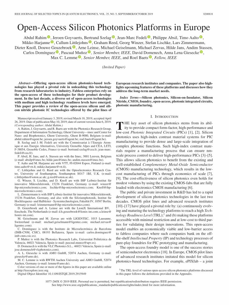
In 2006, Soref proposed to expand the Si photonics technol-ogy to the long-wave infrared region, advocating that the co-integration of group IV photonics with appropriately designedIII-V heterostructures, could be effectively translated to the Mid-IR wavelength band [3–12 μm] to obtain fully integrated opticaldevices [80], [81]. The applications addressed by these tech-nologies include free-space data communication, optical coun-termeasures, IR imaging of biological tissues, spectroscopy andmany others. However, the most mature field of use is the de-tection of traces of chemicals in gaseous, liquid or solid phases.Due to its high absorption, silicon oxide is not allowed in thiswavelength band. CEA-LETI has developed a technology plat-form for PIC fabrication based on SiGe materials on 200 mm Siwafers. For applications in the 3–8 μm range, the waveguidesare composed of a SiGe40% core surrounded by Si cladding. Inthe 8–12 μm range, the waveguides are composed of a pure epi-taxial Ge surrounded by SiGe cladding [82]. The TRL is around5 to 6. VTT has also demonstrated low-loss (0.1–0.5 dB/cm)operation in both 4 and 11 μm thick SOI waveguides at 3.4 μmwavelength. Absorption in silicon oxide has been avoided byusing an air cladding (see Fig. 12).
The technologies are accessible through the European MIR-PHAB pilot line via the website http://www.mirphab.eu/ andthe broker CMP. It is an open access service with a focus onindustrial users. Dedicated runs of a limited number of wafersare used for specific prototyping. Based on a design rule man-ual for each technology, the design can be optimized for eachapplication.
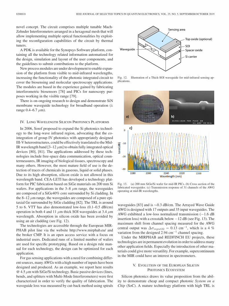
For gas sensing applications with a need for combining differ-ent sources, many AWGs with a high number of inputs have beendesigned and produced. As an example, we report here results@ 4.5μm with SiGe/Si technology. Basic passive devices (lines,bends, and splitters with Multi-Mode Interferometers) were firstcharacterized in order to verify the quality of fabrication. Thewaveguide loss was measured by cut-back method using spirals
Fig. 12. Illustration of a Thick-SOI waveguide for mid-infrared sensing ap-plications.
Fig. 13. (a) 200 mm SiGe/Si wafer for mid-IR PICs. (b) Cross section of thefabricated waveguides. (c) Transmission response of 31 channels of the AWGoperating at mid-IR wavelengths.
waveguides [83] and is ∼0.3 dB/cm. The Arrayed Wave GuideAWG is designed with 17 outputs and 35 input waveguides. TheAWG exhibited a low-loss normalized transmission (−1.6 dBinsertion loss) with a crosstalk below −12 dB (see Fig. 13). Themaximum shift from channel spacing measured for the AWGcentral output was Δσinput22 = 0.13 cm−1, which is a 4 %variation from the designed 2.94 cm−1 channel spacing.
Under the MIRPHAB and REDFINCH EU projects, thesetechnologies are in permanent evolution in order to address manyother application fields. Especially the introduction of other ma-terials could give more versatility. For example, supercontinuumin the MIR could have an interest in spectrometers.
V. EVOLUTION OF THE EUROPEAN SILICON
PHOTONICS ECOSYSTEM
Silicon photonics draws its value proposition from the abil-ity to demonstrate cheap and compact photonic System on aChip (SoC). A mature technology platform with high TRL is

RAHIM et al.: OPEN-ACCESS SILICON PHOTONICS PLATFORMS IN EUROPE 8200818
one element to demonstrate high-density photonic SoC usingsilicon photonics. Equally important are Electronic-PhotonicDesign Automation (EPDA) tools for the design of photonicSoCs, and advanced packaging and assembly tools/techniquesto test them. In the last few years, the European silicon pho-tonics ecosystem has consolidated to offer a complete supplychain to transform a design idea into a functional integrated pho-tonic system. On the design side, the interoperability betweenphysical level simulation tools, circuit level simulation tools,system-level simulation/emulation environments and electronicdesign tools has increased. Similarly, for the packaging andassembly aspects, a broad range of solutions have emerged.This includes techniques for fiber to chip coupling or PICto PIC coupling, DC/RF electrical interfacing with PICs, as-sembly of electrical ICs and photonic ICs, handling of ther-mal and mechanical issues for packaging, and standardised testprotocols. The above-mentioned packaging and assembly so-lutions for small volumes are provided by the PIXAPP pack-aging pilot lines. The pilot lines also provide scale-up routestowards larger volume silicon PIC packaging and assembly[6], [85].
VI. SUMMARY
Open-access of silicon photonics is of vital importance toenable the uptake of this technology by industry. The siliconphotonics open-access model emulates the proven methodologyused by electronics. In Europe, various types of open-access sil-icon photonics technologies are offered to address the needs ofdifferent market sectors. The maturity of the European open-access platforms enables routes for scalable volume manufac-turing of PICs.
APPENDIX
The TRL of open-access silicon photonics platforms dis-cussed in this paper are defined by using the below defined crite-ria. The definitions of these TRLs are determined by translatingthe TRL definitions outlined by the European Commission [84].� TRL 1, 2 and 3: not applicable� TRL 4: PIC process flow successfully developed and
demonstrated in a laboratory environment, typically withresearch-oriented tools
� TRL 5: PIC process flow successfully developed in an en-vironment with manufacturing-grade tools or wafer-levelprototyping tools
� TRL 6: PIC process flow successfully and reproduciblydemonstrated (with a yield acceptable for prototyping) inan environment with manufacturing-grade tools or wafer-level prototyping tools
� TRL 7: Prototyping (including MPW-based prototypingor dedicated full-wafer prototyping) of market-relevantproducts by means of a PIC process flow that has beensuccessfully and reproducibly demonstrated (with a yieldacceptable for at least prototyping) in an environmentcapable of manufacturing or wafer-level prototyping
� TRL 8: PIC process flow qualified with respect to man-ufacturing requirements (yield, turn-around-time, qualityassurance) in an environment capable of manufacturing
� TRL 9: PIC process flow used for competitive manufactur-ing at least at low and/or high-volume level
Hereby the following definitions are used for various open-access modalities:� MPW-based prototyping: up to 100 chips per order.� Prototyping: typically one to a few wafers per order.� Low-volume manufacturing: up to 50 wafers per order.� Medium-volume manufacturing: up to 500 wafers per
order.� High-volume manufacturing: beyond 500 wafers per order.
REFERENCES
[1] M. Salib et al., “Silicon photonics,” Intel Technol. J., vol. 8, no. 2,pp. 143–160, May 2004.
[2] B. Jalali and S. Fathpour, “Silicon photonics,” J. Lightw. Technol., vol. 24,no. 12, pp. 4600–4615, Dec. 2006.
[3] W. Bogaerts et al., “Nanophotonic waveguides in silicon-on-insulatorfabricated with CMOS technology,” J. Lightw. Technol., vol. 23, no. 1,pp. 401–412, Jan. 2005.
[4] S. K. Selvaraja et al., “Highly uniform and low-loss passive silicon pho-tonics devices using a 300 mm CMOS platform,” in Proc. Opt. FiberCommun. Conf. Exhib., San Francisco, CA, USA, 2014, pp. 1–3, doi:10.1364/OFC.2014.Th2A.33.
[5] T. Mogami et al., “High-performance silicon photonics process platformfor low-power photonic integrated circuits,” in Proc. IEEE Silicon Nano-electron. Workshop, Honolulu, HI, USA, 2016, pp. 216–217.
[6] A. Rahim et al., “Open-access silicon photonics: Current status andemerging initiatives,” Proc. IEEE, vol. 106, no. 12, pp. 2313–2330,Dec. 2018.
[7] P. Dumon, “Towards fabless silicon photonics,” in Proc. Front. Opt.2008/Laser Sci. XXIV/Plasmonics Metamaterials/Opt. Fabr. Test., OSATech. Dig., 2008, Paper FMG1.
[8] P. Dumon and A. Khanna, “Foundry technology and services for Si photon-ics,” in Proc. Conf. Lasers Electro-Opt. Pacific Rim, Kyoto, Japan, 2013,pp. 1–2.
[9] M. Hochberg and T. Baehr-Jones, “Towards fabless silicon photonics,”Nature Photon., vol. 4, pp. 492–494, 2010.
[10] P. Absil et al., “Reliable 50Gb/s silicon photonics platform for next-generation data center optical interconnects,” in Proc. 63rd Int. Electron.Device Meeting, San Francisco, CA, USA, 2017, pp. 34.2.1–34.2.4.
[11] B. Szelag et al., “Multiple wavelength silicon photonic 200 mm R+Dplatform for 25Gb/s and above applications,” in Proc. Silicon Pho-ton. Photon. Integr. Circuits V, 2016, vol. 9891, Paper 98911C, doi:10.1117/12.2228744.
[12] D. Knoll et al., “BiCMOS silicon photonics platform for fabrication ofhigh-bandwidth electronic-photonic integrated circuits,” in Proc. IEEE16th Topical Meeting Silicon Monolithic Integr. Circuits RF Syst., Austin,TX, USA, 2016, pp. 46–49.
[13] E. Timurdogan et al., “AIM process design kit (AIMPDKv2.0): Siliconphotonics passive and active component libraries on a 300 mm wafer,” inProc. Opt. Fiber Commun. Conf., 2018, Paper M3F.1.
[14] T. Aalto et al., “3 micron silicon photonics,” in Proc. Opt. Fiber Commun.Conf., San Francisco, CA, USA, 2018, pp. 1–3.
[15] T. Horikawa et al., “A 300-mm silicon photonics platform for large-scaledevice integration,” IEEE J. Sel. Topics Quantum Electron., vol. 24, no. 4,pp. 1–15, Jul./Aug. 2018, Art no. 8200415.
[16] T. Liow et al., “Silicon modulators and germanium photodetectors onSOI: Monolithic integration, compatibility, and performance optimiza-tion,” IEEE J. Sel. Topics Quantum Electron., vol. 16, no. 1, pp. 307–315,Jan./Feb. 2010.
[17] X. Chen et al., “The emergence of silicon photonics as a flexibletechnology platform,” Proc. IEEE, vol. 106, no. 12, pp. 2101–2116,Dec. 2018.
[18] M. Hochberg et al., “Silicon photonics: The next fabless semiconductorindustry,” IEEE Solid-State Circuits Mag., vol. 5, no. 1, pp. 48–58, winter2013.

8200818 IEEE JOURNAL OF SELECTED TOPICS IN QUANTUM ELECTRONICS, VOL. 25, NO. 5, SEPTEMBER/OCTOBER 2019
[19] A. E. Lim et al., “Review of silicon photonics foundry efforts,” IEEE J.Sel. Topics Quantum Electron., vol. 20, no. 4, pp. 405–416, Jul./Aug. 2014,Art no. 8300112.
[20] A. E.-J. Lim et al., “Path to silicon photonics commercialization: Thefoundry model discussion,” in Silicon Photonics III Systems and Applica-tions, Eds. P. Lorenzo and D. J. Lockwood. Berlin, Germany: Springer,2016.
[21] P. De Dobbelaere et al., “Advanced silicon photonics technology platformleveraging a semiconductor supply chain,” in Proc. IEEE Int. ElectronDevices Meeting, San Francisco, CA, USA, 2017, pp. 34.1.1–34.1.4.
[22] G. Q. Lo et al., “The foundry model for silicon photonics-technology,challenges, and opportunities,” in Proc. Conf. Lasers Electro-Opt., SanJose, CA, USA, 2012, pp. 1–3.
[23] A. Jovic et al., “A MEMS actuator system for an integrated 3-D opticalcoherent tomography scanner,” J. Microelectromechanical Syst., vol. 27,no. 2, pp. 259–268, Apr. 2018.
[24] Y. Li et al., “Six-beam homodyne laser Doppler vibrometry based onsilicon photonics,” Opt. Express, vol. 26, pp. 3638–3645, 2018.
[25] C. V. Poulton et al., “Coherent solid-state LIDAR with silicon photonicoptical phased arrays,” Opt. Lett. vol. 42, pp. 4091–4094, 2017.
[26] A. N. Tait et al., “Neuromorphic photonic networks using silicon photonicweight banks,” Scientific Rep., vol. 7, 2017, Art. no. 7430.
[27] M. Lukosevicius et al., “Reservoir computing approaches to recurrent neu-ral network training,” Comput. Sci. Rev., vol. 3, no. 3, pp. 127, 2009.
[28] C.-S. Poon et al., “Neuromorphic silicon neurons and large-scale neuralnetworks: challenges and opportunities,” Front. Neurosci., vol. 5, p. 108,2011.
[29] N. C. Harris et al., “Programmable nanophotonics for quantum simulationand machine learning,” Adv. Photon., 2017, Paper ITu3A.3.
[30] Y. Shen et al., “Deep learning with coherent nanophotonic circuits,” NaturePhoton., vol. 11, pp. 441–446, 2017.
[31] A. Peruzz et al., “Quantum walks of correlated photons,” Science,vol. 329, no. 5998, pp. 1500–1503, Sep. 17, 2010.
[32] S. Paesani et al., “Experimental quantum hamiltonian learning using asilicon photonic chip and a nitrogen-vacancy electron spin in diamond,”in Proc. Conf. Lasers Electro-Opt. Europe Eur. Quantum Electron. Conf.,Munich, Germany, 2017, pp. 1–1.
[33] M. Pantouvaki et al., “50Gb/s silicon photonics platform for short-reachoptical interconnects,” in Proc. Opt. Fiber Commun. Conf., OSA Tech.Dig., 2016, Paper Th4H.4.
[34] P. De Heyn et al., “Ultra-dense 16 × 56Gb/s NRZ GeSi EAM-PD arrayscoupled to multicore fiber for short-reach 896Gb/s optical links,” in Proc.Opt. Fiber Commun. Conf., OSA Tech. Dig., 2017, Paper Th1B.7.
[35] J. Zhang et al., “Transfer-printing-based integration of a III-V-on-silicon distributed feedback laser,” Opt. Express, vol. 26, pp. 8821–8830,2018.
[36] D.-X. Xu et al., “Silicon photonic integration platform have we foundthe sweet spot?” IEEE J. Sel. Topics Quantum Electron., vol. 20, no. 4,pp. 189–205, Jul./Aug. 2014.
[37] B. Szelag et al., “Optimization of 64 Gbps O-band thin-rib PN junctionMach-Zehnder Modulator fabricated on a 200 mm silicon photonics plat-form,” in Proc. Int. Conf. Solid State Devices Mater., 2018, pp. 495–496.
[38] L. Virot et al., “Integrated waveguide PIN photodiodes exploiting lateralSi/Ge/Si heterojunction,” Opt. Express, vol. 25, no. 16, pp. 19487–19496,2017.
[39] Q. Wilmart et al., “Si-SiN photonic platform for CWDM applications,” inProc. IEEE 15th Conf. Group IV Photon., 2018, pp. 1–2.
[40] G. Winzer et al., “Monolithic photonic-electronic QPSK receiver for28Gbaud,” in Proc. Opt. Fiber Commun. Conf. Exhib., Los Angeles, CA,USA, 2015, pp. 1–3.
[41] S. Lischke et al., “Performance improvement of a monolithically integratedC-Band receiver enabled by an advanced photonic BiCMOS process,” inProc. IEEE Bipolar/BiCMOS Circuits Technol. Meeting, Miami, FL, USA,2017, pp. 50–53.
[42] G. R. Mehrpoor et al., “64-GBd DP-Bipolar-8ASK transmission over 120km SSMF employing a monolithically integrated driver and MZM in 0.25-µm SiGe BiCMOS technology,” presented at the Opt. Fiber Commun.Conf., San Diego, CA, USA, 2019, Paper Tu2A.5.
[43] T. Aalto et al., “Low-loss converters between optical silicon waveguidesof different sizes and types,” IEEE Photon. Technol. Lett. vol. 18, no. 5,pp. 709–711, Mar. 2006.
[44] M. Cherchi et al., “Dramatic size reduction of waveguide bendson a micron-scale silicon photonic platform,” Opt. Express, vol. 21,pp. 17814–17823, 2013.
[45] K. Vysrokinos et al., “DPSK-demodulation based on ultra-compactmicron-scale SOI platform,” in Proc. Opt. Fiber Commun. Conf., 2015,Paper W2A.14.
[46] D. Jalas et al., “Faraday rotation in silicon waveguides,” in Proc. 14th Int.Conf. Group IV Photon., Berlin, Germany, 2017, pp. 141–142.
[47] M. Pagani et al., “Low-error and broadband microwave frequency mea-surement in a silicon chip,” Optica, vol. 2, no. 8, pp. 751–756, 2015.
[48] H. Fueser et al., “56 Gb/s WDM transmitter module based on siliconmicrorings using comb lasers,” in Proc. Conf. Lasers Electro-Opt., QELS-Fundam. Sci., 2015, Paper JTh2A–66.
[49] D. Schall et al., “Graphene photodetectors with a bandwidth 76 GHzfabricated in a 6” wafer process line,” J. Phys. D, Appl. Phys., vol. 50,no. 12, 2017, Paper 124004.
[50] D. Schall et al., “Infrared transparent graphene heater for silicon photonicintegrated circuits,” Opt. Express, vol. 24, no. 8, pp. 7871–7878, 2016.
[51] N. Iliadis et al., “16 × 1 Packaged MUX/DEMUX for flexible-grid opticalnetworks,” J. Lightw. Technol., vol. 35, no. 14, pp. 3050–3059, Jul. 2017.
[52] A. L. Giesecke et al., “Ultra-efficient interleaved depletion modulatorsby using advanced fabrication technology,” in Proc. 42nd Eur. Conf. Opt.Commun., 2016, pp. 1067–1069.
[53] G. T. Reed et al., “Silicon optical modulators,” Nature Photon., vol. 4,pp. 518–526, 2010.
[54] D. J. Thomson et al., “50 Gbit/s silicon optical modulator,” IEEE Photon.Technol. Lett., vol. 24, no. 4, pp. 234–236, Feb. 2012.
[55] D. Perez et al., “General-purpose silicon photonics processor core,” NatureCommun., vol. 8, p. 636, 2017.
[56] R. Marchetti et al., “High-efficiency grating-couplers: demonstration of anew design strategy,” Scientific Rep., vol. 7, 2017, Art. no. 166770.
[57] D. T. Spencer et al., “An optical-frequency synthesizer using integratedphotonics,” Nature, vol. 557, pp. 81–85, 2018.
[58] L. Chang et al., “Heterogeneous integration of lithium niobate and siliconnitride waveguides for wafer-scale photonic integrated circuits on silicon,”Opt. Lett., vol. 42, pp. 803–806, 2017.
[59] Brasch et al., “Photonic chip based optical frequency comb using soli-ton Cherenkow radiation,” Science, vol. 351, no. 6271, pp. 357–360, Sci-ence2016.
[60] D. J. Blumenthal et al., “Silicon nitride in silicon photonics,” Proc. IEEE,vol. 106, no. 12, pp. 1–23, Dec. 2018.
[61] C. G. Roeloffzen et al., “Low-loss Si3N4 TriPleX optical waveguides:Technology and applications overview,” IEEE J. Sel. Topics QuantumElectron., vol. 24, no. 4, pp. 1–21, Jul./Aug. 2018.
[62] K. Worhoff et al., “TriPleX: A versatile dielectric photonic platform,” Adv.Opt. Technol., vol. 4, no. 2, pp. 189–207, 2015.
[63] PiX4life, Pilot line. [Online]. Available: www.pix4life.eu[64] M. Mahmud-Ul-Hasan et al., “Suppression of bulk fluorescence noise
by combining waveguide-based near-field excitation and collection,” ACSPhoton., vol. 4, no. 3, pp. 495–500, 2017.
[65] S. Kerman et al., “Integrated nanophotonic excitation and detection offluorescent microparticles,” ACS Photon., vol. 4, no. 8, pp. 1937–1944,2017.
[66] A. Dhakal et al., “Evanescent excitation and collection of spontaneousRaman spectra using silicon nitride nanophotonic waveguides,” Opt. Lett.,vol. 39, pp. 4025–4028, 2014.
[67] A. Z. Subramanian et al., “Low-loss singlemode PECVD silicon nitridephotonic wire waveguides for 532–900 nm wavelength window fabricatedwithin a CMOS pilot line,” IEEE Photon. J., vol. 5, no. 6, Dec. 2013, Artno. 2202809.
[68] H. Jans et al., “Integrated bio-photonics to revolutionize health care en-abled through PIX4life and PIXAPP,” in Proc. SPIE Nanoscale Imag.,Sens., Actuation Biomed. Appl. XV, Feb. 20, 2018, vol. 10506, Paper105060V.
[69] D. Martens et al., “Compact silicon nitride arrayed waveguide grat-ings for very near-infrared wavelengths,” Photon. Technol. Lett., vol. 27,no. 2, pp. 137–140, 2015.
[70] M. A. Piqueras et al., “Photonic front-end for the next-generation of spaceSAR applications,” in Proc. 10th Eur. Microw. Integr. Circuits Conf., Paris,France, 2015, pp. 301–304.
[71] G. Dabos et al., “Plasmonic stripes in aqueous environment co-integratedwith Si3N4Photonics,” IEEE Photon. J., vol. 10, no. 1, 2018, Art. no.2700108.
[72] P. Cegielski et al., “Monolithically integrated perovskite semicon-ductor lasers on silicon photonic chips by scalable top-down fab-rication,” Nano Lett., vol. 18, no. 11, pp. 6915–6923, 2018, doi:10.1021/acs.nanolett.8b02811.

RAHIM et al.: OPEN-ACCESS SILICON PHOTONICS PLATFORMS IN EUROPE 8200818
[73] P. Cegielski et al., “Integrated perovskite lasers on a silicon nitride wave-guide platform by cost-effective high throughput fabrication,” Opt. Ex-press, vol. 25, no. 11, pp. 4624–4629, 2017.
[74] M. Mohsin et al., “Graphene based on-chip variable optical attenuatoroperating at 855 nm wavelength,” Opt. Express, vol. 25, no. 25, pp. 31660–31669, 2017.
[75] P. Munoz et al., “Silicon nitride photonic integration platforms for visi-ble, near-infrared and mid-infrared applications,” Sensors, vol. 17, no. 9,p. 2088, 2017, doi: 10.3390/s17092088.
[76] L. A. Bru et al., “Integrated optical frequency domain reflectometry devicefor characterization of complex integrated devices,” Opt. Express, vol. 26,no. 23, 2018, Art. no. 30000, doi: 10.1364/OE.26.030000.
[77] D. Perez et al., “Field-programmable photonic arrays,” Opt. Express,vol. 26, no. 21, pp. 27265–27278, 2018, doi: 10.1364/OE.26.027265.
[78] K. E. Zinoviev et al., “Integrated bimodal waveguide interferometricbiosensor for label-free analysis,” J. Light. Technol., vol. 29, no. 13,pp. 1926–1930, Jul. 2011, doi: 10.1109/JLT.2011.2150734.
[79] J.-C. Tinguely, Ø. I. Helle, and B. S. Ahluwalia, “Silicon nitride wave-guide platform for fluores-cence microscopy of living cells,” Opt. Express,vol. 25, no. 22, pp. 27678–27690, 2017, doi: 10.1364/OE.25.027678.
[80] R. A. Soref et al., “Silicon waveguided components for the long-waveinfrared region,” J. Opt. Pure Appl. Opt., vol. 8, no. 10, p. 840, Oct. 2006.
[81] R. Soref, “Group IV photonics for the mid infrared,” in Proc. SPIESilicon Photon. VIII, Mar. 2013, vol. 8629, Paper 86290214, doi:10.1117/12.2013769.
[82] J. Fedeli and S. Nicoletti, “Mid-infrared (Mid-IR) silicon-based pho-tonics,” Proc. IEEE, vol. 106, no. 12, pp. 2302–2312, Dec. 2018 doi:10.1109/JPROC.2018.2844565.
[83] R. G. Hunsperger, Integrated Optics: Theory and Technology, 3rd ed. NewYork, NY, USA: Springer, 1991.
[84] [Online]. Avaialbale: https://ec.europa.eu/research/participants/data/ref/h2020/wp/2014_2015/annexes/h2020-wp1415-annex-g-trl_en.pdf. Ac-cessed on: Mar. 4, 2019.
[85] J. Fedeli et al., “EU pilot lines for integrated photonics,” in Proc. IEEE14th Int. Conf. Group IV Photon., Berlin, Germany, 2017, pp. 79–80.
Abdul Rahim received the master’s degree in elec-trical engineering with emphasis on photonics fromthe KTH Royal Institute of Technology, Stockholm,Sweden, and Ghent University, Ghent, Belgium, from2006 to 2008, and received the doctorate degree fromTechnische Universität Berlin, Berlin, Germany, forhis work on investigating novel silicon photonic in-tegrated filters for optical communication systems.He is currently a Postdoc with Professor Roel Baetswith the Photonics Research Group, Ghent Univer-sity, Ghent, Belgium. Apart from his involvement in
silicon photonics research activities at Photonics Research Group, he is the co-ordinator of ePIXfab, the European Silicon Photonics Alliance. From 2009 to2014, he worked with the Research Group of Professor Klaus PetermannHismaster’s studies were funded by the Erasmus Mundus program of the EuropeanCommission. He was a part of the sensors and system’s team of a public sectororganization in Pakistan from 2003 to 2006 and was with the Advanced ResearchDepartment of Laird Technologies, Sweden, in 2008. He holds one patent andhas authored/coauthored several publications in high impact peer-reviewed jour-nals and conferences.
Jeroen Goyvaerts received the M.Sc. degrees innanoscience and nanotechnology from the CatholicUniversity of Leuven, Leuven, Belgium, and in pho-tonics from the Polytechnic University of Catalunya,Barcelona, Spain. Since September 2016, he hasbeen with the Photonics Research Group, GhentUniversity. There, his work is primarily focused onSiN biosensors for low-power applications in thePIX4LIFE project.
Bertrand Szelag received the master’s degree inphysics from the University of Lille, Lille, France,in 1994, and the Ph.D. degree in microelectronicsfrom the University of Grenoble, Grenoble, France,in 1999. He has been a Visiting Researcher with To-hoku University in 1997 working in the field of sub-100 nm CMOS transistor properties. In 1999, he jointSTMicroelectronics in Crolles, France, to work onBiCMOS platfrom development for Analog/RF ap-plications. Since 2013, he has been with the LETI,MINATEC Institute, Grenoble, France, as a Project
Manager and Senior Process Integration Researcher in the field of silicon pho-tonic devices. He has authored or coauthored more than 50 papers in scientificjournals and international conference proceedings in the field of CMOS, Bipo-lar, and DMOS transistors and silicon photonic devices. His current researchactivities included high speed silicon modulator, germanium photodetectors,and hybrid III-V laser integration in silicon.
Jean-Marc Fedeli received the Electronics EngineerDiploma from INPG Grenoble, Grenoble, France, in1978. Then, he was involved at CEA-LETI in the de-velopment of various magnetic memories and mag-netic components as a Project Leader, Group Leader,and Program Manager. For two years, he was theAdvanced Program Director with the Memscap Com-pany for the development of RF-MEMS, then hereturned to CEA-LETI in 2002 as a Coordinator ofSilicon Photonic Projects until 2012. Under a largerresearch partnership, he works on many technological
aspects on photonics on CMOS (Si rib and stripe waveguides, a-Si waveguides,slot waveguides), Si modulators, Ge photodetectors, InP integrated sources onSi. He has been participating in different European projects such as EPIXFABfor MPW circuit fabrication and has coordinated the FP7 PLAT4M project onSilicon Photonics Platform. Since 2014, he has moved to sensing activities withphotonics, and he is currently the Technical Manager of the H2020 MIRPHABpilot line on liquid and gas systems sensors. His H factor is around 35 with morethan 200 publications and 50 patents. He has authored three book chapters (oneon magnetic recording and two on silicon photonics).
Philippe Absil received the Ph.D. degree from theDepartment of Electrical Engineering, University ofMaryland, College Park, MD, USA, in 2000. His doc-toral work contributed to the early demonstrations ofsemiconductor microring resonators. He is currentlythe Director of the 3-D and Optical I/O TechnologiesDepartment at Imec since 2013 and has been respon-sible for the silicon photonics technology platformdevelopment since 2010. Before that he spent sevenyears managing the advanced CMOS scaling programat Imec. In the early 2000s, he developed the passive
photonics platform technology for Little Optics, Inc., Annapolis Junction, MDUSA.
Timo Aalto received the M.Sc. and D.Sc. degrees inoptoelectronics technology from Helsinki Universityof Technology, Espoo, Finland, in 1998 and 2004,respectively. He has worked at VTT in Espoo, Fin-land, since 1997 with the primary research focus onsilicon photonics, making him one of the pioneers inthe field. He currently leads the Photonics Integrationteam that operates in VTT’s two clean room facili-ties, Micronova in Espoo, and Micromodule centre inOulu. He has authored 80 refereed journal and con-ference papers, one book chapter, and more than ten
granted patents. He is a member of EOS and Photonics Finland. Relating to thesuccessful business development in silicon photonics, he was the recipient ofthe VTT Award in 2014.

8200818 IEEE JOURNAL OF SELECTED TOPICS IN QUANTUM ELECTRONICS, VOL. 25, NO. 5, SEPTEMBER/OCTOBER 2019
Mikko Harjanne received the M.Sc. degree in op-toelectronics from Helsinki University of Technol-ogy, Espoo, Finland, in 2003. He joined VTTsintegrated optics group in 2000 and his current focusis on the design and simulation of optical circuits. Hehas authored 14 journal articles and 37 refereed con-ference papers. He is a member of Photonics Finland.
Callum Littlejohns received the First Class Hon-ors degree in electronic engineering from the Univer-sity of Surrey, Guildford, U.K., and the Ph.D. degreein the field of silicon photonics from the Optoelec-tronics Research Centre, University of Southampton,Southampton, U.K., in March 2015. He is currently aResearch Fellow with Nanyang Technological Uni-versity, Singapore, but remains part of the SiliconPhotonics Group as a Visitor. His work has been pub-lished in multiple peer-reviewed journals includingScientific Reports, a Nature Publishing Group jour-
nal. His work was also selected as a prestigious postdeadline paper at the IEEEGroup IV Photonics conference in Paris, 2014. The work completed during hisPh.D. has been protected by two separate patents, both fully supported by theUniversity of Southampton. He has a track record of excellence, has been therecipient of the multiple awards throughout his academic life, including the In-formation Overload category winner at the 2015 EPSRC ICT Pioneers Awardand the runner-up prize in the Best Student Poster Award at the 2014 Optoelec-tronics Research Centre Photonics Day.
Graham Reed is currently a Professor of silicon pho-tonics and Group Leader. He joined the University ofSouthampton, Southampton, UK, in 2012 from theUniversity of Surrey, Guildford, UK, where he wasProfessor of Optoelectronics, and was Head of theDepartment of Electronic Engineering from 2006 to2012. He is a pioneer in the field of silicon photonics,and acknowledged as the individual who initiated theresearch field in the UK. He established the SiliconPhotonics Research Group at the University of Sur-rey in 1989. The first silicon photonics company in
the world, Bookham Technology, Inc., was founded by Reed’s Ph.D. student, Dr.A. Rickman, and adopted the research developed in the Group. The Silicon Pho-tonics Group has provided a series of world leading results since its inception,and is particularly well known for its work on silicon optical modulators. He hasauthored or coauthored more than 500 papers in the field of silicon photonics.Prof. Reed is a regular invited and contributing author to the major silicon pho-tonics conferences around the world. He has served on numerous internationalconference committees. He is currently a member of five international confer-ence committees.
Georg Winzer received the Dipl. Ing. degree in electrical engineering from theTechnical University Berlin, Berlin, Germany, in 2012, and is currently work-ing toward the Ph.D. degree. Starting in 2006, he worked with the center forHochfrequenztechnik-Photonic at Technische Universität Berlin on layout andmeasurement of photonic integrated circuits. Since 2012, he has been with IHPMicroelectronics, Frankfurt, Germany, where his research interests include thedesign and layout of PIC and EPIC devices, high-speed O/E device characteri-zation, and the setup of a photonic design-kit.
Stefan Lischke received the B.Sc. and M.Sc. de-grees in physics with specialization in semiconductortechnology from the Technical University Branden-burg, Cottbus, in 2005 and 2007, respectively, and thePh.D. degree in physics from the Technical Univer-sity Berlin, Berlin, Germany, in 2017. He is currentlya Researcher with the Silicon Photonics Group withinthe Technology Department of IHP—Leibniz-Institutfr innovative Mikroelektronik, Frankfurt, Germany.His current work is focused on Germanium photo de-tectors and the integration of photonic devices into
IHP’s photonic BiCMOS technology. He was the recipient of the several BestPaper Awards.
Lars Zimmermann was born in Germany. Hereceived a higher education (undergraduate) fromFriedrich-Schiller University, Jena, Germany, BrunelUniversity London, London, U.K., and TU Delft,Delft, The Netherlands, and the Ph.D. degreefrom IMEC, Leuven, Belgium, in 2003. He movedto Belgium for his postgraduate studies at KatholiekeUniversiteit Leuven. In Leuven, he was affiliated withIMEC where he worked for five years. His scientificwork at IMEC dealt with the development of extendedshort-wave infrared detector arrays and sensor assem-
bly processes. In 2004, he moved to TU Berlin. In Berlin, he worked for fiveyears on silicon-based optical motherboard technology, realizing early hybridassemblies of silicon waveguides with lasers, semiconductor optical amplifiers,and detectors. In 2008, he moved to IHP, the Leibniz Institute für innovativeMikroelektronik. At IHP, he directs the silicon photonics activities. In 2018, here-joined TU Berlin where he is currently a Professor in the field of silicon pho-tonics. He is also a Team Leader Silicon photonics at IHP, coordinating the co-operation with TU Berlin in the field of Silicon photonics within the frame of theJoint Lab Silicon Photonics. His current work is focusing on high-performancephotonic-electronic integration for optical communications and for nonlinearoptical signal processing.
Dieter Knoll received the Diploma degree in physicsfrom the Technical University of Chemnitz (the for-mer Karl-Marx-Stadt), Chemnitz, Germany, in 1974,and the Ph.D. degree in applied physics from theAcademy of Sciences of the GDR, Berlin, Germany,in 1988. From 1974 to 2017, he has been with IHPin Frankfurt, Germany, where he was engaged in re-search on the fabrication of silicon-based devices andcircuits. He is currently a consultant in the field ofphotonics integration. His research interests includednpn-SiGe-base and SiGe:C-base bipolar transistors,
pnp bipolar transistors, BiCMOS technology, and Si photonics.
Douwe Geuzebroek received the Ph.D. degree inelectrical engineering from the University of Twente,Enschede, The Netherlands, at the Integrated Op-tical MicroSystem Group on a topic of applyingintegrated optical microring resonators in telecom-munication networks. He is currently with the VPMarketing and Sales at LioniX International. He hasmore than 15 years of experience in integrated pho-tonics and its applications, ranching from R&D toproduct development stages. He has a strong interestin matching the technical aspect of a technology to
the needs of the market. In 2005, he joined LioniX BV as a Design Engineerand Project Leader focusing on microring resonators and other integrated opti-cal telecommunication devices and was actively involved in the startup of XiOPhotonics in 2008. As VP Marketing and Sales at XiO Photonics, he supportedthe development of the waveguide technology for visible light applications andthe introduction of this technology in several products. He participated in sev-eral research projects both national and European. Currently, as VP Marketingand Sales at LioniX International, he is involved in the acquisition of new com-mercial and research projects for photonic integrated modules in life science,metrology, and telecommunication applications.

RAHIM et al.: OPEN-ACCESS SILICON PHOTONICS PLATFORMS IN EUROPE 8200818
Arne Leinse received the Ph.D. degree in the inte-grated optical microsystems group from the Univer-sity of Twente, Enschede, The Netherlands, in 2005.He is currently active in integrated optics for morethan 15 years. Hereafter, he joined LioniX BV wherehe was involved in the invention and development ofthe TriPle platform from the beginning. He has beeninvolved from the original concept until the exploita-tion and (co)authored more than 100 articles in thelast years. He has been active as a Vice-President ofLioniX BV in the last years and since the establish-
ment of LioniX-international in 2016 active in the role of Chief CommercialOfficer.
Michael Geiselmann received the degree inphysics and engineering from the University ofStuttgart, Stuttgart, Germany, the graduate degreefrom the Ecole Centrale Paris, France, in 2008, and thePh.D. degree from the Institute of Photonic Sciences,Barcelona, Spain, in 2014. He joined the Laboratoryof Prof. Kippenberg at EPFL, Lausanne, Switzerland,where he advanced frequency comb generation on in-tegrated silicon nitride chips towards applications. Hewas leading several international research projects. In2016, he cofounded LIGENTEC. As a Managing Di-
rector, he is responsible for strategy, sales, and business development. He coau-thored more than 18 publications and over 20 conference contributions.
Michael Zervas received the B.S. and M.S. de-grees in applied mathematics and applied physicsfrom Athens Technical University, Athens, Greece, in2005, and the M.Sc. degree in micro and nano tech-nologies for integrated systems, joint master’s degreereceived by the Ecole Polytechnique Federale de Lau-sanne (EPFL), Lausanne, Switzerland, Institut Na-tional Polytechnique de Grenoble, Genoble, France,and Politecnico di Torino, Turin, Italy, in 2007, andthe Ph.D. degree from the Department of ElectricalEngineering, EPFL, under the supervision of Prof.
Leblebici in the area of nanofabrication, in 2013.From 2007 to 2010, he was with Oerlikon, first as a Management Trainee
and later as a Strategic Procurement Manger, Singapore for Oerlikon Solar (twoyears). He was with IBM from 2012 to mid 2013 under CMOSAIC Project asan Research Associate and with the Intel from 2013 to 2014, as a Process En-gineer for the 14-nm node. After rejoining EPFL, as a Scientist in mid 2014, hecofounded LIGENTEC, Lausanne, Switzerland, in 2016, where he is advancingthe technology development of silicon nitride based integrated circuits.
Hilde Jans received the Ph.D. degree in chemistryfrom the Catholic University of Leuven, Leuven, Bel-gium, in 2010. She is a Senior Researcher with theExperimental Bio-Photonics Team of the LSI Depart-ment. Her main activity is to link the (bio-) applica-tion to the technology under development in the team.Since 2011, her focus is on Raman spectroscopy ap-plications as she is involved in many project, bothbilateral and European projects.
Andim Stassen received the B.S. degrees in physicsand molecular biology and genetics from IstanbulTechnical University, Istanbul, Turkey, and the M.S.degree in nanoscience and nanotechnology fromCatholic University of Leuven, Leuven, Belgium, in2010. In the same year, she joined Life Science Tech-nologies Department at imec. She is currently work-ing as a Process Integration Engineer for life scienceapplications and she is responsible of the SiN pho-tonics platform development.
Carlos Domínguez received the B.S., M.S., andPh.D. degrees in chemistry from the UniversidadComplutense of Madrid, Madrid, Spain, in 1980, and1985, respectively. He became a member of the sci-entific staff at the Instituto de Microelectrnica deBarcelona (IMB-CNM, CSIC) in 1986. Since 2002,he has been a Research Professor. In 1992, he foundedthe Chemical Transducers Group within the institute,having today 28 researchers and technicians, and hasbeen recognized as a Technological Transfer Centerby the Catalan Government. He is a member of the
Spanish Royal Society of Chemistry, the Committee of Optoelectronics and In-tegrated Optics of the Spanish Optical Society, and a member of the InternationalCommittee of Ibersensor. Also a member of the Association EPIC (EuropeanPhotonic Industry Consortium) Technology Platform Photonics21, and formermember of SECPhO Technology Cluster (Cluster of Southern Europe Photon-ics and Optics). He is involved in materials and process development for newtransducers and sensor devices, authored or coauthored around 165 papers inthis area. He is currently working on the development of an integrated opticaltechnology based on silicon and silicon compounds for (bio)-chemical sensorsand broadband telecommunications applications.
Pascual Muñoz was born in Valencia, Spain, onFebruary 7, 1975. He received the Ingeniero deTelecomunicacion degree and the Ph.D. degree inphotonics from Universitat Politecnica de Valencia(UPV), Valencia, Spain, in 1998 and 2003, respec-tively. In 1999, he served as 1st Lieutenant in theSpanish Airforce, while working as IT consultant forAIME Instituto Tecnologico. He is currently an As-sociate Professor with the Departamento de Comu-nicaciones, and a Researcher with the Institute forTelecommunications and Multimedia Applications,
both at UPV. He runs a consolidated research line, started in 2005, on prototyp-ing Photonic Integrated Circuits (PICs) in a technology agnostic fashion, wherePICs are designed in the best suited technology (Silicon-On-Insulator, IndiumPhosphide, Silica on Silicon, Silicon Nitride amongst other) for each applica-tion. He has been involved in several European Commission funded projects,being coordinator for integration on InP within the NoE IST-EPIXNET. He hasauthored or coauthored more than 40 papers in international refereed journalsand more than 60 conference contributions. He is a member of the TechnicalProgramme Committees of the European Conference on Optical Communica-tions and the European Conference on Integrated Optics. He was the recipientof the VPI Speed Up Photonics Award in 2002 for innovative Fourier opticsAWG with multimode interference couplers modeling, by Virtual Photonics In-corporated and the IEEE COMMUNICATIONS MAGAZINE. He was also grantedthe IEEE/LEOS Graduate Student Fellowship Program in 2002. He was alsothe recipient of the extraordinary doctorate prize from UPV in 2006. From hisresearch line, he cofounded the UPV spin-off company VLC Photonics in 2011,where the PIC design know-how, expertise and tools have been transferred, andhe served as CEO from 2011 to 2013. He is a Senior Member of the OSA.

8200818 IEEE JOURNAL OF SELECTED TOPICS IN QUANTUM ELECTRONICS, VOL. 25, NO. 5, SEPTEMBER/OCTOBER 2019
David Domenech was born in Alfafar, Valencia,Spain. He received the B.Sc. degree in telecommu-nications from the Escuela Politecnica Superior deGandia, Valencia, Spain, in 2006, the M.Sc. degree intechnologies, systems and networks of communica-tion from the Universidad Politecnica de Valencia,Valencia, Spain, in 2008, and the Ph.D. degree inphotonics from the Universitat Politecnica de Valen-cia within the Optical and Quantum CommunicationsGroup in 2013. He has been involved in several na-tional and international research projects. He has au-
thored or coauthored more than ten papers in international refereed journals andmore than 20 conference contributions. He was the recipient of the Intel doctoralstudent honor programme award in 2012 in recognition for his work during hisPh.D. He is a Cofounder and CTO of the spin-off company VLC Photonics,devoted to the design of photonics integrated circuits in multiple integrationtechnologies.
Anna Lena Giesecke received the Diploma degreefrom Leibniz University, Hannover, Germany, and thedoctoral degree in physics from Heinrich-Heine Uni-versity, Dsseldorf, Germany. She joined AMO GmbHin 2013 and is the Head of the nanophotonics group.She has been working in the research fields of ul-trafast laser sources, plasma physics, and photonicintegrated circuits based on silicon and silicon nitrideas well as optoelectronic devices. One of her currentresearch interests is the integration of light sourcesinto dielectric platforms.
Max C. Lemme received the Dipl.-Ing. and Dr.-Ing.degrees in electrical engineering from RWTH AachenUniversity, Aachen, Germany. He is currently a Pro-fessor of electronic devices with RWTH Aachen Uni-versity and the Director of AMO GmbH, Aachen.His current research interests include electronic, op-toelectronic, and nanoelectromechanical devices andsensors made from novel materials like graphene andrelated 2-D materials, Perovskites or phase changematerials and their integration into the silicon tech-nology platform.
Roel Baets received the M.Sc. degree in electricalengineering from UGent in 1980 and a second M.Sc.degree from Stanford in 1981, and the Ph.D. degreefrom UGent in 1984. He is currently a Full Professorwith Ghent University (UGent) and is part-time as-sociated with IMEC. From 1984 till 1989, he held aPostdoctoral Position with IMEC. Since 1989, he hasbeen a Professor with the Faculty of Engineering andArchitecture of UGent where he founded the Photon-ics Research Group. From 1990 till 1994, he has alsobeen a part-time Professor with Delft University of
Technology and from 2004 till 2008 at Eindhoven University of Technology. Hehas mainly worked in the field of integrated photonics. He has made contribu-tions to research on photonic integrated circuits, both in III-V semiconductorsand in silicon, as well as their applications in telecom, datacom, sensing, andmedicine. Web of Science reports more than 600 publications with an h-indexwell over 60. As part of a team of eight professors he leads the Photonics Re-search Group. With about 90 researchers this group is involved in numerous(inter)national research programs and has created six spin-off companies. Thesilicon photonics activities of the group are part of a joint research initiativewith IMEC. He has led major research projects in silicon photonics in Europe.In 2006, he founded ePIXfab, the globally first Multi-Project-Wafer service forsilicon photonics. Since then ePIXfab has evolved to become the European Sil-icon Photonics Alliance. He is also the Director of the multidisciplinary Centerfor Nano- and Biophotonics (NB Photonics) at UGent, founded in 2010. Hewas a cofounder of the European M.Sc. programme in Photonics. He is anERC grantee of the European Research Council and a Methusalem grantee ofthe Flemish government. He is a Fellow of the IEEE, of the European OpticalSociety, and of the Optical Society. He is also a member of the Royal Flem-ish Academy of Belgium for Sciences and the Arts. He has been a recipientof the 2011 MOC Award and of the 2018 PIC-International Lifetime Achieve-ment Award. He is Director-at-Large with the Board of Directors of The OpticalSociety.