operational amplifier stability part 7 of 15: when...
TRANSCRIPT

Operational Amplifier Stability Part 7 of 15: When Does RO Become ZO?
By Tim Green Linear Applications Engineering Manager, Burr-Brown Products from Texas Instruments
A funny thing happened on the way to writing about "There must be six ways to leave your capacitive load stable." http://www.analogzone.com/acqt0704.pdf We chose a CMOS operational amplifier with a "rail-to-rail" output and measured the ROUT, where there was no loop gain, at high frequency, to determine RO. From this measurement we predicted a second pole location in the amplifier's "modified Aol plot" due to a 1 µF capacitive load. To our surprise our Tina SPICE simulation for this modified Aol plot was off by a factor of x5! This error was way outside of the acceptable bounds of any of our past first-order analysis and thereby launched a detailed investigation of op amp output impedance. Here in Part 7 we focus on op amp open-loop output impedance, ZO, for the two most common output topologies for small signal op amps. For traditional bipolar emitter-follower op amp output stages ZO is well behaved and predominantly resistive (RO) throughout the unity-gain bandwidth. However, for many CMOS rail-to-rail output op amps ZO is both capacitive and resistive, within the unity-gain bandwidth of the amplifier. We will not, in this Part, analyze the bipolar topology known as all npn output, which is most commonly used in power op amps (capable of operating in a linear region with high output currents from 50 mA to greater than 10 A). Our expanded knowledge of output impedance will be critical to our correct prediction of modified Aol plots and an essential tool in our network synthesis techniques for stable op amp circuits. ZO for Bipolar Emitter-Follower Output Op Amps A classical bipolar output stage of emitter-follower topology is shown in Fig. 7.1. With this type of output stage, RO (small-signal, open-loop output resistance) is usually the dominant portion of ZO (small-signal, open-loop output impedance). As well, RO is usually constant for a given dc current load. We will examine some rules-of-thumb for emitter-follower RO and then use these rules of thumb to predict RO for various values of dc output current. We will then check our predictions using Tina SPICE simulations.

Fig. 7.1: Typical Emitter-Follower, Bipolar Output Op Amp
A typical emitter-follower, bipolar output op amp's specifications are shown in Fig. 7.2. This topology often yields low noise, low drift input specifications with the input bias currents in the nA-region (eg 10 nA). Some bipolar op amps use JFETs in the input stages to reduce input bias currents down to the low pA-range. The common-mode input range will usually be about 2 V from either supply. The output voltage swing is typically restricted to within 2 V or more of either supply rail and these op amps commonly get the best performance from using dual supplies (eg ±5 V to ±15 V).
Fig. 7.2: Example Specifications: Emitter-Follower, Bipolar Output Op Amp
A simplified model for the classic emitter-follower, bipolar op amp uses two GM (current gain) stages followed by a transistor voltage-follower output (see Fig. 7.3). ZO, the open-loop output impedance, is dominated by RO, open-loop output resistance, and is constant over the unity-gain bandwidth.
OPA227High Precision, Low Noise Bipolar Operational Amplifier
Input Specs AC SpecsOffset Voltage 75uV max Open Loop Gain, RL = 10k 160dB typOffset Drift 0.6uV/C Open Loop Gain, RL = 600 160dB typInput Voltage Range (V-)+2V to (V+)-2V Gain Bandwidth Product 8 MHzCommon-Mode Rejection Ratio 138dB typ Slew Rate 2.3V/usInput Bias Current 10nA max Overload Recovery Time 1.3us
Total Harmonic Distortion + Noise 0.00005%, f=1kHzSetling Time, 0.01%
Noise Supply SpecsInput Voltage Noise 90nVpp, f=0.1Hz to 10Hz Specified Voltage Range +/-5V to +/-15VInput Voltage Noise Density 3nV/rt-Hz @1kHz Quiescent Current +/-3.8A maxInput Current Noise Density 0.4pA/rt-Hz Over Temperature +/-4.2A max
Output Specs Temperature & PackageVsat @ Iout = 1.2mA 2V max Operating Range -40C to +85CVsat @ Iout = 19mA 3.5V max Package options SO-8, DIP-8, DIP-14, SO-14Iout Short Circuit +/-45mA

Two GM (current gain) StagesOutput is Voltage Output Follower
Open Loop Output Impedance (ZO) is dominated by ROConstant RO over Op Amp Unity Gain Bandwidth
-
+
GM1
-
+GM2
-
+
-
+
VCV1
R1 100k R2 100kVout
-Input
+Input
CC 10p
Ro 33
Fig. 7.3: Two-Stage Simplified Model: Emitter-Follower, Bipolar Output Op Amp For most amplifiers the Class-AB bias current in the output stage (with no load) is about half of the quiescent current for the entire amplifier. For bipolar transistors RO is proportional to 1/gm, where gm is the current transfer ratio or current gain. Since gm is proportional to collector current IC then we see that RO is inversely proportional to IC. As IC increases from no-load to full-load output current RO will decrease. This might imply that if we pull extremely high currents that RO would go to zero. However, due to the physics of the transistor and the internal drive and bias arrangement this is not the case. We will measure RO at the highest useable load current and define it as RX. We will then measure RO at no load current and derive a constant, KZ, for the given op amp circuitry that will enable us to predict what RO does with any load current. From Fig. 7.4 we clearly see how the term emitter-follower output describes the path to the output pin of the op amp from the front end gm stages.
QM TIP30
RP 5
RM 5
VCC 15
VEE 15
QP TIP31
A+
IABA+
Iinput
A+
Iq
Vout
Input+
Input- -
+ +
U1 OPA227
A-BBias
ZO = RORO ~ (1/gm) + RXgm ~ IC/VBE
RO= (1/IC)KZ + RXwhere:1) KZ is derived at No
Load RO. 2) RX is minimum RO
due to output transistor and bias circuitry. Derived at heavy load current.
At small load currents RO 1/IC
At large load currents RO = RX
Im
Ip
IAB = 1/2 Iq
Fig. 7.4: ZO Definition: Emitter-Follower, Bipolar Output Op Amp
Fig. 7.5 details our emitter-follower ZO model with a constant value RX, measured at full load current, and a series current-dependent resistor, with the transfer function of KZ ÷ IC. Since we have a push (pnp transistor) output stage and a pull (npn transistor) output stage our ZO model includes equivalent RO models for each stage. The effective small-signal ac output impedance looking back into the output

pin will be the parallel combination of the push and pull output stages. Remember that for our small-signal ac model of ZO both power supplies, VCC and VEE, will appear as an ac short.
RX 1k
RX 1k
VCC 15
VEE 15
VOUT
RPip 5k
RMim 5k
A+
Ip
A+
Im
RX 1k
RX 1k
VOUT
RPip 5k
RMim 5k
VCC = Short f or small signal AC
VEE = Short f or small signal AC
RPip = KZ / Ip
RMim = KZ / Im
RPip = KZ / Ip
RMim = KZ / Im
Simplifies to
Fig. 7.5: ZO Model: Emitter-Follower, Bipolar Output Op Amp
Not A
ll M
acro
-mod
els
are
Equa
l
Fig. 7.6: Not All SPICE Op Amp Models Are Equal!

Not all SPICE macro-models for op amps are equal (Fig. 7.6). As such, any simulations we do to investigate output impedance, ZO, must be done on macro-models which correctly model the output with real devices and proper Class-AB bias circuitry which accurately models the actual device. It is not often clear from a given manufacturer if this is adequately modeled. Most SPICE models for precision op amps developed by the Burr-Brown division of Texas Instruments, over the last 4 years, were built by W K Sands of Analog & RF Models (http://www.home.earthlink.net/%7Ewksands/). These SPICE models of the op amp are extremely good representations of the actual silicon op amp and as shown above will include a detailed list of features including proper modeling of the output stage as well as the Class-AB bias circuitry.
Since we were not able to find a bipolar emitter-follower op amp macro-model with accurate Class-AB biasing and real transistor outputs for an accurate analysis of real world behavior we built our own for evaluation purposes.
VCC
VEE
VCC
VEE
QM MRF5211LT1
RP 5
RM 5
VOUT
Itest
VCC 15
VEE 15
A+
IP
A+
IM
Vdc 27m
RL 1
LF 1T
QP MRF5711LT1
-
+
-
+
x100M
QD MRF5211LT1
QAB1 MRF5711LT1
QAB2 MRF5711LT1
R2 1k
VF1
R1
900
IS1 2m
A +
IOUT
DC = 0AAC = 1Apk
27mA
-1.23V
260.44nA
26.88mA
27mV
QP on and QM essentially offso QP sets output impedance
Fig. 7.7: ZO, Heavy Load IOUT = +27mA In Fig. 7.7 we see an ideal front end implemented with a voltage-controlled-voltage source with open loop gain of 160dB (x100E6). The output transistors, QP and QM, are biased on with a simplified Class-AB bias circuit. For our op amp we set the maximum output current at 27 mA and therefore to find our RO parameter RX we will test with a load current of +27mA. A simple ZO test circuit in Tina SPICE is easy to build through the use of an input resistor RL and a feedback inductor LF. At dc the inductor is a short and RL, combined with the applied voltage, Vdc, sets the dc load current as shown. With our ideal 1 TH (1E12 henry) inductor we have a dc closed-loop path so SPICE can find an operating point, but for any ac frequency of interest we have an open circuit. Now if we excite our circuit with a 1 A, ac source, Itest, then VOUT becomes ZO after a math conversion from dB. Notice for this heavy load (IOUT =+27 mA) that QM is essentially off and QP is on and dominates the output impedance.

We see (Fig. 7.8) our measured results for ZO with IOUT = +27 mA out of our bipolar emitter-follower output op amp. The initial SPICE results will be plotted in linear-dB. If we choose logarithmic on the y-axis this will result directly in ohms for ZO. The logarithmic scale on the y axis will become handy when we look at other ZO plots that are not constant over the frequency bandwidth (ie CMOS RRO).
T
Zo (IOUT = +27mA)
Frequency (Hz)10 100 1k 10k 100k 1M 10M
Zo (o
hms)
1.00
100.00
Zo (IOUT = +27mA)
Zo A:(206.7k; 6.39)
a
Fig. 7.8: ZO AC Plot, Heavy Load, IOUT = +27mA
RX 6.39
RX 6.39
VOUT
RPip 0
RMim 100M
RPip = KZ / Ip
RMim = KZ / Im
Ip = 27mAAs sume RPip = 0 ohm
As sume Im = 0ARMim > 100M ohm
Fig. 7.9: Heavy-Load ZO Model
In our equivalent heavy-load ZO model for IOUT = +27 mA (Fig. 7.9) RX was measured to be 6.39 Ω. We will assume that the output transistors (QP and QM) used are close in characteristics and therefore assign RX the same value for each. If we wanted we could re-run our analysis and measure RX for IOUT = -27 mA. The results would be close enough for us to ignore the difference. From this model we assume RMim will be high impedance and therefore have no measurable effect on RO. Also we assume RPip will be much smaller than RX.

VCC
VEE
VCC
VEE
QM MRF5211LT1
RP 5
RM 5
VOUT
Itest
VCC 15
VEE 15
A+
IP
A+
IM
Vdc 0
RL 1
LF 1T
QP MRF5711LT1
-
+
-
+
x100M
QD MRF5211LT1
QAB1 MRF5711LT1
QAB2 MRF5711LT1
R2 1k
VF1R
1 90
0
IS1 2m
A +
IOUT
DC = 0AAC = 1Apk
14.82nA
-1.48V
1.07mA
1.08mA
14.82nVIAB
QP and QM are equally biased on and contribute equally to ZO
Fig. 7.10: ZO, No Load, IOUT = 0mA The no-load condition for our Class-AB bias emitter-follower (Fig. 7.10) has the bias current, IAB, set to 1.08 mA. We see that both output transistors, QP and QM, are on and both contribute equally to ZO. The no-load ZO is measured as 14.8 Ω (Fig. 7.11) which, with the heavy-load value for ZO (with a result for RX) allows us to complete our small-signal ZO model by computing the constant KZ.
T
Zo (No Load)
Frequency (Hz)10 100 1k 10k 100k 1M 10M
Zo (o
hms)
1.00
100.00
Zo (No Load)
Zo A:(124.46k; 14.8)
a
Fig. 7.11: ZO Ac Plot, No Load, IOUT = 0 mA

In Fig. 7.12 we use our emitter-follower ZO model for the no-load condition. With results from the heavy-load condition fill in values for RX. Derive KZ based on ZO at no load assuming that the characteristics of both QP and QM are similar. The derivation (in Fig. 7.12) finds KZ to be 0.0250668.
Fig. 7.12: No-Load ZO Model
So now let's test our emitter-follower ZO model. We will use a dc current out of QP of 2.54 mA (about 2 x IAB -- twice the Class-AB bias current.) This should turn off QM and force ZO to be dominated by the RO due to QP and (Fig. 7.13) we see this is approximately true. This is a good illustration as how real world Class-AB bias schemes work. As load current increases positively the entire Class-AB bias current begins to shift into QP. As the load current goes negative, QM begins to receive the entire Class-AB bias current until QP is completely turned off at heavy negative load currents.
Both QP and QM on and contribute to ZO but QP dominates due to lowest impedance
VCC
VEE
VCC
VEE
QM MRF5211LT1
RP 5
RM 5
VOUT
Itest
VCC 15
VEE 15
A+
IP
A+
IM
Vdc 2.16m
RL 1
LF 1T
QP MRF5711LT1
-
+
-
+
x100M
QD MRF5211LT1
QAB1 MRF5711LT1
QAB2 MRF5711LT1
R2 1k
VF1
R1
900
IS1 2m
A +
IOUT
DC = 0AAC = 1Apk
2.16mA
-1.45V
387.41uA
2.54mA
2.16mV
Fig. 7.13: ZO, Light Load, IOUT = +2xIAB (2.16 mA)

In our emitter-follower light-load ZO model (Fig. 7.14) we use our known values of RX and KZ to compute the equivalent ZO we expect and then run our Tina SPICE simulation (results in Fig. 7.15). We expected ZO at light load to be 13.2326 Ω with Tina SPICE measuring 12.85 Ω. This is close enough to use for any analysis we are interested in. If we took the time to investigate we would find that QP and QM do not have exactly the same characteristics.
Fig. 7.14: Light-Load ZO Model
T
Zo (IOUT = +2.16mA)
Frequency (Hz)10 100 1k 10k 100k 1M 10M
Zo (o
hms)
1.00
100.00
Zo (IOUT = +2.16mA)
Zo A:(140.24k; 12.85)
a
Fig. 7.15: ZO Ac Plot, Light Load, IOUT = +2.16 mA

Now our complete set of curves for emitter-follower ZO can be constructed (see Fig. 7.16) where ZO is dominated by RO, constant over the unity-gain bandwidth of the op amp, and RO goes down with increasing load currents. Notice that ZO was plotted for both source and sink currents at light load and heavy load with no significant difference in source or sink ZO. These key curves for ZO should be included in every bipolar emitter follower op amp data sheet.
T
Zo (No Load)
Zo (IOUT = -2.16mA): 12.93Zo (IOUT = +2.16mA): 12.85
Zo (IOUT = -27mA): 6.5
Zo (IOUT = +27mA): 6.39
Frequency (Hz)10 100 1k 10k 100k 1M 10M
Zo (o
hms)
1.00
100.00
Zo (No Load)
Zo (IOUT = +2.16mA): 12.85 Zo (IOUT = -2.16mA): 12.93Zo (IOUT = +27mA): 6.39
Zo (IOUT = -27mA): 6.5
No Load
Light Load
Heavy Load
Fig. 7.16: Complete ZO Curves: Bipolar Emitter-Follower
ZO And Capacitive Loads For Bipolar, Emitter-Follower Output Op Amps
U1: Op Amp DC and AC Aol FunctionVCV1: x1 Voltage-Controlled-Voltage-SourceRo: Open Loop AC Small Signal Output ResistanceCL modifies Aol Curve.
Fig. 7.17: Bipolar Emitter-Follower ZO and Capacitive Loads For capacitance loads on the output of emitter-follower stages we will use the model in Fig. 7.17. We are either given in a data sheet, or can measure, the op amp's Aol curve with no capacitive load. RO will react with CL and form a second pole, fp2, in the op amp's unloaded Aol curve.

VCC
VEE
VCC
VEE
QM MRF5211LT1
RP 5
RM 5
VCC 15
VEE 15
A+
IP
A+
IM
QP MRF5711LT1
-
+
-
+
x100M
QD MRF5211LT1
QAB1 MRF5711LT1
QAB2 MRF5711LT1
R2 1k
VF1
R1
900
IS1 2m
LT 1G
CT 1G
CL 10n
+
VG1
VOA
VM
Aol = VOA / VM
Fig. 7.18: Tina SPICE Circuit for Modified Aol Measurement We will load our emitter-follower bipolar op amp with many different capacitive loads and test it for the location of the additional pole, fp2, due to RO and CL. Fig. 7.18 uses LT (as a short-circuit) to establish a dc operating point. At any ac frequency of interest LT is open-circuit so we can look at a modified Aol curve. CT is open for dc and a short for any ac frequency of interest and connects the ac test source, VG1, into circuit. By inspection we see that Aol = VOA ÷ VM. The resultant modified Aol curves due to several different capacitive loads are shown in Fig. 7.19. T
CL = 1nFfp2 = 9.71MHz
CL = 10nFfp2 = 1.07MHz
CL = 100nFfp2 = 107kHz
CL = 1000nFfp2 = 10.77kHz
CL = 10,000nFfp2 = 1.08kHz
No Load
Frequency (Hz)10 100 1k 10k 100k 1M 10M
Gai
n (d
B)
0.00
20.00
40.00
60.00
80.00
100.00
120.00
140.00
160.00
fp2
CL = 10,000nFfp2 = 1.08kHz
CL = 1000nFfp2 = 10.77kHz
CL = 100nFfp2 = 107kHz
CL = 10nFfp2 = 1.07MHz
CL = 1nFfp2 = 9.71MHz
No Load
Fig. 7.19: Modified Aol Curves for Different Values of CL
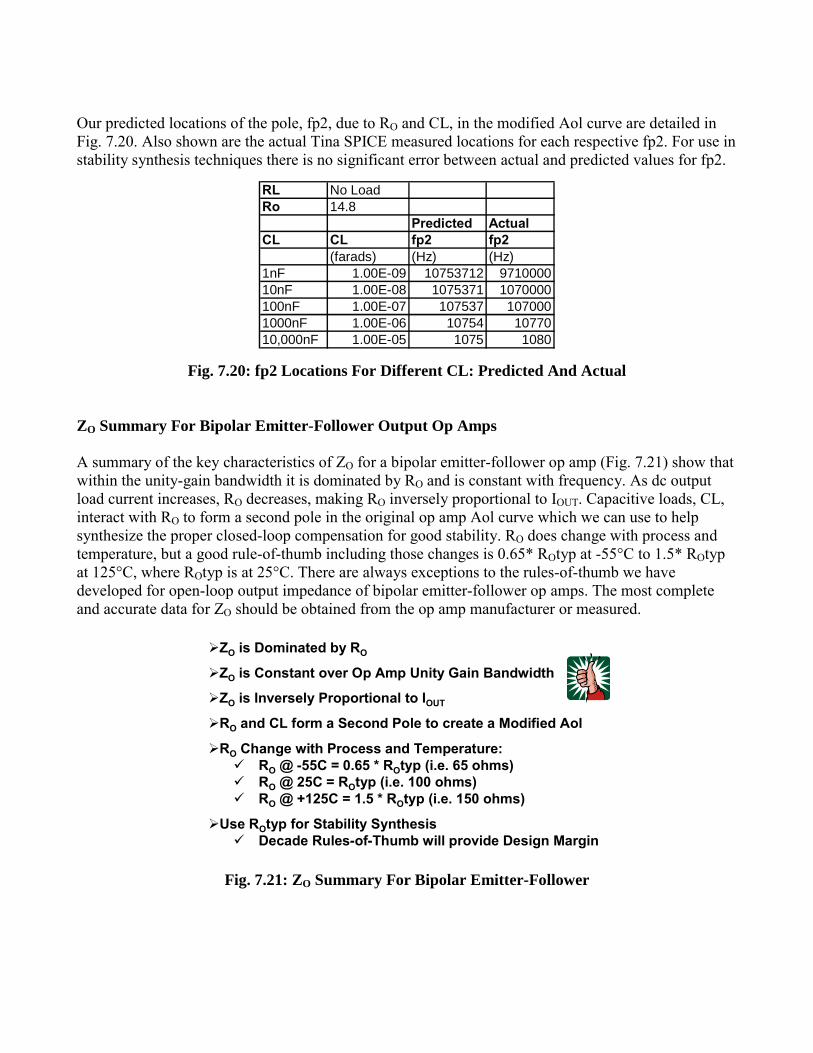
Our predicted locations of the pole, fp2, due to RO and CL, in the modified Aol curve are detailed in Fig. 7.20. Also shown are the actual Tina SPICE measured locations for each respective fp2. For use in stability synthesis techniques there is no significant error between actual and predicted values for fp2.
RL No LoadRo 14.8
Predicted ActualCL CL fp2 fp2
(farads) (Hz) (Hz)1nF 1.00E-09 10753712 971000010nF 1.00E-08 1075371 1070000100nF 1.00E-07 107537 1070001000nF 1.00E-06 10754 1077010,000nF 1.00E-05 1075 1080
Fig. 7.20: fp2 Locations For Different CL: Predicted And Actual
ZO Summary For Bipolar Emitter-Follower Output Op Amps A summary of the key characteristics of ZO for a bipolar emitter-follower op amp (Fig. 7.21) show that within the unity-gain bandwidth it is dominated by RO and is constant with frequency. As dc output load current increases, RO decreases, making RO inversely proportional to IOUT. Capacitive loads, CL, interact with RO to form a second pole in the original op amp Aol curve which we can use to help synthesize the proper closed-loop compensation for good stability. RO does change with process and temperature, but a good rule-of-thumb including those changes is 0.65* ROtyp at -55°C to 1.5* ROtyp at 125°C, where ROtyp is at 25°C. There are always exceptions to the rules-of-thumb we have developed for open-loop output impedance of bipolar emitter-follower op amps. The most complete and accurate data for ZO should be obtained from the op amp manufacturer or measured.
ZO is Dominated by RO
ZO is Constant over Op Amp Unity Gain Bandwidth
ZO is Inversely Proportional to IOUT
RO and CL form a Second Pole to create a Modified Aol
RO Change with Process and Temperature: RO @ -55C = 0.65 * ROtyp (i.e. 65 ohms) RO @ 25C = ROtyp (i.e. 100 ohms) RO @ +125C = 1.5 * ROtyp (i.e. 150 ohms)
Use ROtyp for Stability Synthesis Decade Rules-of-Thumb will provide Design Margin
Fig. 7.21: ZO Summary For Bipolar Emitter-Follower
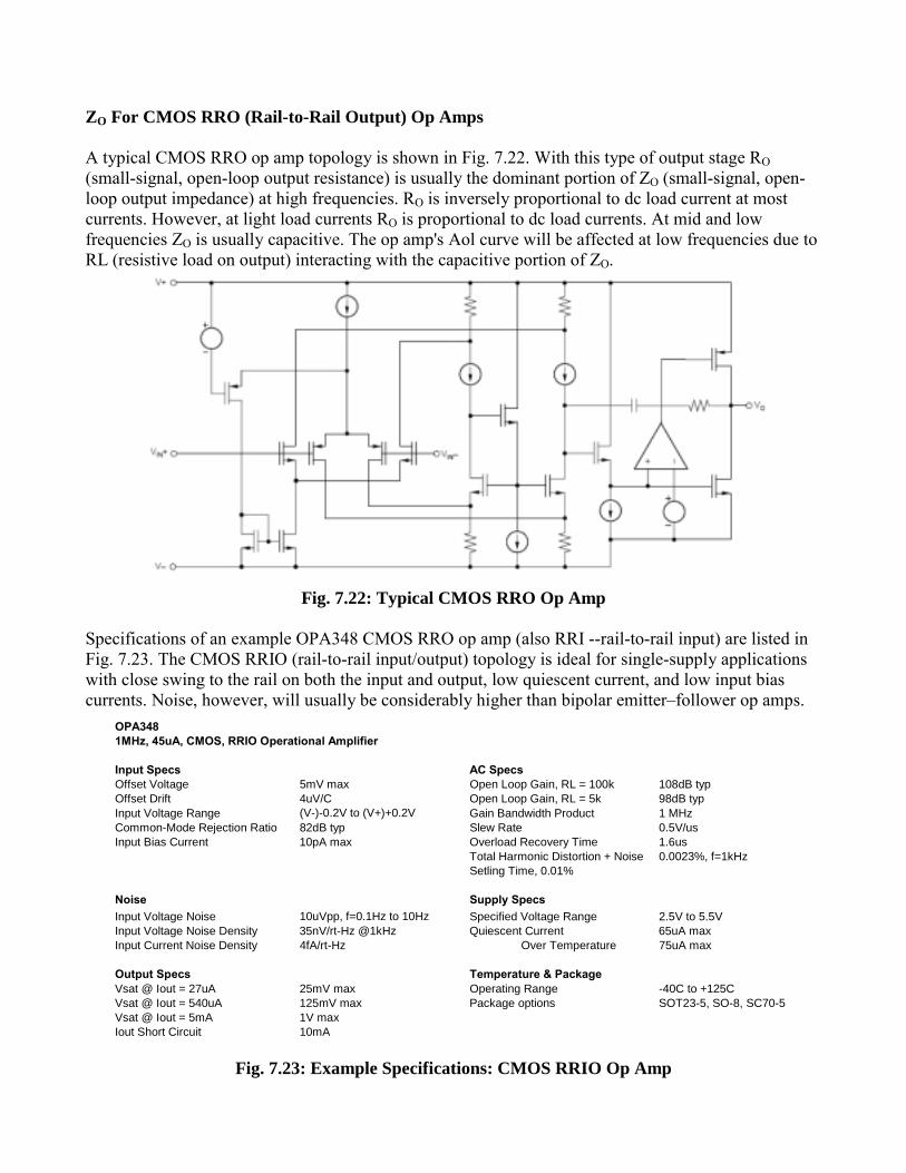
ZO For CMOS RRO (Rail-to-Rail Output) Op Amps A typical CMOS RRO op amp topology is shown in Fig. 7.22. With this type of output stage RO (small-signal, open-loop output resistance) is usually the dominant portion of ZO (small-signal, open-loop output impedance) at high frequencies. RO is inversely proportional to dc load current at most currents. However, at light load currents RO is proportional to dc load currents. At mid and low frequencies ZO is usually capacitive. The op amp's Aol curve will be affected at low frequencies due to RL (resistive load on output) interacting with the capacitive portion of ZO.
Fig. 7.22: Typical CMOS RRO Op Amp Specifications of an example OPA348 CMOS RRO op amp (also RRI --rail-to-rail input) are listed in Fig. 7.23. The CMOS RRIO (rail-to-rail input/output) topology is ideal for single-supply applications with close swing to the rail on both the input and output, low quiescent current, and low input bias currents. Noise, however, will usually be considerably higher than bipolar emitter–follower op amps.
Fig. 7.23: Example Specifications: CMOS RRIO Op Amp
OPA3481MHz, 45uA, CMOS, RRIO Operational Amplifier
Input Specs AC SpecsOffset Voltage 5mV max Open Loop Gain, RL = 100k 108dB typOffset Drift 4uV/C Open Loop Gain, RL = 5k 98dB typInput Voltage Range (V-)-0.2V to (V+)+0.2V Gain Bandwidth Product 1 MHzCommon-Mode Rejection Ratio 82dB typ Slew Rate 0.5V/usInput Bias Current 10pA max Overload Recovery Time 1.6us
Total Harmonic Distortion + Noise 0.0023%, f=1kHzSetling Time, 0.01%
Noise Supply SpecsInput Voltage Noise 10uVpp, f=0.1Hz to 10Hz Specified Voltage Range 2.5V to 5.5VInput Voltage Noise Density 35nV/rt-Hz @1kHz Quiescent Current 65uA maxInput Current Noise Density 4fA/rt-Hz Over Temperature 75uA max
Output Specs Temperature & PackageVsat @ Iout = 27uA 25mV max Operating Range -40C to +125CVsat @ Iout = 540uA 125mV max Package options SOT23-5, SO-8, SC70-5Vsat @ Iout = 5mA 1V maxIout Short Circuit 10mA

Fig. 7.24 is a simplified model for a CMOS RRO op amp using a voltage output differential front end which controls a current source, GM2. GM2 drives RO, developing a voltage which controls GMO, the output current source. Capacitor CO feeds back into the RO/GM2 node. From this simplified model we observe that at high frequencies ZO = RO. As we go from high frequency towards medium and low frequencies we expect to see the effects of CO and will therefore look for ZO to be capacitive.
Output is two GM (current gain) StagesOutput is Current Source GMO (ideal current source has infinite impedance)
Output Impedance (ZO) is dominated by RO at High FrequenciesZO will look capacitive at Low and Medium Frequencies
Fig. 7.24: Simplified Model: CMOS RRO Op Amp
In most CMOS RRO amplifiers (Fig. 7.25) the Class-AB bias current in the output stage (with no load) is about half of the quiescent current for the entire amplifier. At high frequencies ZO = RO and proportional to gm (current transfer ration for MOSFET). But, for MOSFETs, gm is inversely proportional to the square-root of ID (drain current).
VCC 5
A+
IABA+
Iinput
A+
Iq
Vout
Input+
Input- -
+ +
U1 OPA227QP 2N6804
QM 2N6755
A-BBias
At High Frequencies:ZO = RO
RO ~ (1/gm) gm ~ 2√(K*ID)
RO 12√(K*ID)
Im
Ip
IAB = 1/2 Iq
Fig. 7.25: ZO Definition: CMOS RRO Op Amp

Fig. 7.26 details our CMOS RRO RO model consisting of current-controlled resistors for each half of the push (QP) and pull (QM) output MOSFETs. Each of these resistors, RPip and RMim, are proportional to the square root of the ID flowing through each respective MOSFET. When looking back into the output terminal of the op amp these two current-controlled resistors appear in parallel for a net value of RO. The equation for the parallel combination of these resistances creates a mathematical equation which yields an unexpected transfer function. For small increases in IOUT, RO will increase until one of the output MOSFETS gets completely turned off and out of Class-AB bias mode.
VCC 2.5
VEE 2.5
VOUT
RPip 400
RMim 400
A+
Ip
A+
Im
VOUT
RPip 5k
RMim 5k
VCC = Short f or small signal AC
VEE = Short f or small s ignal AC
Simplifies to
Fig. 7.26: RO Model: CMOS RRO Op Amp

CMOS RRO Ro Calculator
K= 0.071
Ip Rp Im Rm Ro2.2000E-05 4.0006E+02 2.2000E-05 4.0006E+02 2.0003E+021.1000E-05 5.6578E+02 3.3000E-05 3.2665E+02 2.0709E+025.5000E-07 2.5302E+03 4.3450E-05 2.8467E+02 2.5588E+025.5000E-08 8.0013E+03 4.3950E-05 2.8305E+02 2.7338E+025.5000E-09 2.5302E+04 4.3990E-05 2.8292E+02 2.7979E+021.0000E-12 1.8765E+06 4.4000E-05 2.8289E+02 2.8285E+02 Ro Max1.0000E-12 1.8765E+06 8.8000E-05 2.0003E+02 2.0001E+021.0000E-12 1.8765E+06 1.7600E-04 1.4144E+02 1.4143E+021.0000E-12 1.8765E+06 3.5200E-04 1.0002E+02 1.0001E+02
Fig. 7.27: Example Of RO Increasing/Decreasing Characteristic
The example calculation (Fig. 7.27) shows the unique relationship of RO for small changes in IOUT. We see a 200 Ω RO when both devices have equal current flowing through QP and QM (22 µA) in the Class-AB bias mode. As Im increases, indicating IOUT is increasing in output current sunk, QP receives less and less current until it is essentially turned off at Im = 44 µA. It is at this point that we see RO at a maximum (RO Max = 282.25 Ω). For higher IOUT currents RO will decrease.
Vee 2.5
RL 10VOA
Itest
LF 1T
Vcc 2.5
V1 101m
+
-
+U2 OPA348
A +
IOUT
DC = 0AAC = 1Apk
10mA
100.03mV
NOTE:IOUT current meter provides accurate measure of IOUTIdeally IOUT = V1 / RL but this does not account for input offset voltage!
Fig. 7.28: ZO, Heavy Load, IOUT = +10 mA
The OPA348 chosen to investigate CMOS RRO ZO has an extremely accurate SPICE macro-model and the ZO characteristics were confirmed through lab bench testing. Tina SPICE allows us a convenient way to look at the characteristics of ZO with our first ZO measurement at the maximum load current of 10 mA. The current meter, IOUT, in our test circuit (Fig. 7.28) ensures that we control the dc value of IOUT to be exactly 10mA. Simply dividing V1 by RL does not exactly account for the input offset voltage characteristics of the op amp, which may add an unacceptable error.

The ac plot of ZO for IOUT of 10 mA (Fig. 7.29) has a high-frequency RO component of 34.79 Ω and ZO is clearly capacitive for frequencies lower than about 10 kHz. We expect at this output current for RO to be the lowest we will see since QM is entirely off, and QP is conducting all the output stage current.
T
Zo (IOUT = +10mA)
Frequency (Hz)1 10 100 1k 10k 100k 1M 10M
Zo (o
hms)
10.00
100.00
1.00k
10.00k
100.00k
1.00M
Zo (IOUT = +10mA)
Ro A:(1.35M; 34.79)
a
Fig. 7.29: ZO Ac Plot, Heavy Load, IOUT = +10 mA Our heavy-load RO model (Fig. 7.30) confirms that at this output current RO should be the lowest since QM is entirely off and QP has all output stage current flowing through it.
VCC 5
A+
IABA+
Iinput
A+
Iq
Vout
Input+
Input- -
+ +
U1 OPA227QP 2N6804
QM 2N6755
A-BBias
QP on and QM essentially off so QP sets output impedance
Fig. 7.30: Heavy-Load RO Model

Our no-load ZO curve will be computed using the circuit in Fig. 7.31. From our rule-of-thumb for IQ Vs IAB we would guess that since IQ = 45 µA, then IAB = 22.5 µA for the OPA348. Our error current of 483.65 fA should not contribute any significant error for our no load ZO curve.
Vee 2.5
RL 10VOA
Itest
LF 1T
Vcc 2.5
V1 0
+
-
+U2 OPA348
A +
IOUT
DC = 0AAC = 1Apk
483.65f A
-163.51f V
Fig. 7.31: ZO, No Load, IOUT = 0 mA
T
Zo (No Load)
Frequency (Hz)1 10 100 1k 10k 100k 1M 10M
Zo (o
hms)
100.00
1.00k
10.00k
100.00k
1.00M
Ro A:(1.13M; 196.75)
Zo (No Load)
a
Fig. 7.32: ZO Ac Plot, No Load, IOUT = 0 mA For IOUT of 0 mA (Fig. 7.32) ZO has a high-frequency RO component of 196.75 Ω. ZO is clearly capacitive for frequencies lower than about 3 kHz.

VCC 5
A+
IABA+
Iinput
A+
Iq
Vout
Input+
Input- -
+ +
U1 OPA227QP 2N6804
QM 2N6755
A-BBias
QP and QM are equally biased on and contribute equally to RO
IAB
Fig. 7.33: No-Load RO Model
Our no-load RO model (Fig. 7.33) shows that inside the OPA348 both output devices, QP and QM, are contributing equally to RO. It also shows an assumed Class-AB bias current of 22.5 µA. We now know what ZO is for heavy load and no load. The other key curve we are interested in is light load where RO becomes biggest but we do not know exactly where this operating point is, not being able to see inside the bias stage, so we need to find this point before we compute an ac transfer curve (Fig. 7.34). Running the analysis/calculate ac nodal voltages analysis continuously, as shown, we vary the value of V1 and get an instant update on VOA -- an rms reading. Setting IG1 to 1 A, ac generator, and f = 1 MHz (well inside the frequency area where RO dominates ZO). Finding a value for V1 that yields maximum VOA we can use it to run our ac transfer curves. With VOA an rms reading it includes any dc component which, for our current levels, would be down in the 7.35 µVrms region -- insignificant when compared to VOA in the 254.56 Vrms region. We expect for this light load that the ac magnitude value for RO will be 254.56 Vrms ÷ 0.707 Arms = 360 Ω (for sine waves).
Run AC Analysis/Calculate Nodal Voltages continuously
Vary V1 to increase IOUT
Look for max VOA value
Fig. 7.34: Light-Load Search For Max RO

Our ZO light-load test circuit is shown Fig. 7.35.
Vee 2.5
VOA
Vcc 2.5
+
-
+U2 OPA348
V1 10u
RL 1
LF 1T
A+
AM1
IG1AC 1ApkDC 0A
7.35uA
7.35uV
Fig. 7.35: ZO, Light Load, IOUT = +7.35 µA Results of our ZO light-load ac transfer function analysis are in Fig. 7.36. We see an RO value of 360 Ω which is what we had predicted and, below about 3 kHz, ZO is capacitive.
T
Zo(IOUT = +7.35uA)
Frequency (Hz)1 10 100 1k 10k 100k 1M 10M
Zo (o
hms)
100.00
1.00k
10.00k
100.00k
1.00M
Zo A:(858.57k; 360)
Zo(IOUT = +7.35uA)
a
Fig. 7.36: ZO Ac Plot, Light Load, IOUT = +7.35 µA For our light load model (see Fig. 7.37) we see that QP is on and QM is just off and so QP will set the value of RO since it will be the lowest impedance. We also see that our original assumption of Class-AB bias being 22.5 µA is probably not correct since it only took 7.35 µA of load current to turn off QM. IAB is probably not much greater than 7.35 µA.

VCC 5
A+
IABA+
Iinput
A+
Iq
Vout
Input+
Input- -
+ +
U1 OPA227QP 2N6804
QM 2N6755
A-BBias
QP on and QM just off so QP dominates due to lowest impedance Fig. 7.37: Light-Load ZO Model
Our complete set of key ZO curves for OPA348 (Fig. 7.38) show our interest in:
• IOUT = +7.35 µA (RO = 360 Ω RO max) • IOUT = no load (RO = 196.75 Ω RO no load) • IOUT = +87.4 µA (RO = 198.85 Ω) IOUT at which RO about equals RO no load • IOUT > 87.4 µA result in RO < RO no load • IOUT = +10 mA (RO = 34.79 Ω)
The remaining curves verify that operating conditions in between will also give results which fall in between. In addition, ZO curves were taken for negative values of IOUT and were so close to laying on the positive values that they were omitted for clarity. These curves should be in all data sheets.
T
IOUT=50uARo=249.98 ohms
IOUT=No LoadRo=196.75 ohms
IOUT=+87.4uARo=198.85 ohms
IOUT=+7.35uARo=360 ohms
IOUT=+1mARo=75.56 ohms
IOUT=+10mARo=34.79 ohms
Frequency (Hz)1 10 100 1k 10k 100k 1M 10M
Zo (o
hms)
10.00
100.00
1.00k
10.00k
100.00k
1.00M
IOUT+ Curves only shownNo significant difference between IOUT+ and IOUT- curves
IOUT=+10mARo=34.79 ohms
Zo vs IOUT+
IOUT=50uARo=249.98 ohms
IOUT=+7.35uARo=360 ohms
IOUT=+1mARo=75.56 ohms
IOUT=+87.4uARo=198.85 ohms
IOUT=No LoadRo=196.75 ohms
Fig. 7.38: Complete ZO Curves: CMOS RRO

For an equivalent ZO model for CMOS RRO op amps we analyze the breakpoint, fz, on our ZO curves (see Fig. 7.39 for heavy and no loads). This, with RO, allows us to determine a value for CO.
T
Zo = 49.208+3dB pointfz = 4.48kHz 34.79
Zo (IOUT = +10mA)
Zo (No Load)
196.78
Zo= 278.33+3dB pointfz = 1.75kHz
Frequency (Hz)1 10 100 1k 10k 100k 1M 10M
Zo (o
hms)
10.00
100.00
1.00k
10.00k
100.00k
1.00M
196.78
Zo= 278.33+3dB pointfz = 1.75kHz
Zo (No Load)
Zo (IOUT = +10mA)
34.79
Zo = 49.208+3dB pointfz = 4.48kHz
Fig. 7.39: fz Breakpoints On ZO Curves From our ZO plots we now complete our model at IOUT no load and heavy load (10 mA) -- Fig. 7.40.
+
--IN
+IN GMOGM2RO
VOUT
CO
+-
+
-
Aol fz = 1 2* *RO*CO
fz RO CONo Load 1.75kHz 196.78 ohms 0.4622uFHeavy Load 4.48kHz 34.79 ohms 1.0211uF
Fig. 7.40: ZO Complete Model Calculations

ZO And Capacitive Loads For CMOS RRO Op Amps For creating modified Aol curves from the original op amp Aol, when we are driving capacitive loads, the load capacitor, CL, will be in series with our ZO model capacitor, CO. Remember that capacitors in series are like resistors in parallel. And so, if CL < CO, CL will dominated and then if CL > CO, CO will dominate. The modified Aol curve second pole, fp2, will depend directly on RO and Ceq, the equivalent capacitance due to CO and CL. Fig. 7.41 illustrates these key points.
Fig. 7.41: Modified Aol fp2 Calculations In our test circuit to plot modified Aol curves due to capacitive loading on the CMOS RRO op amp, OPA348 (Fig. 7.42) the ac loop is opened by LT, but a short for the dc operating point calculation. CT is open for dc but short for any ac frequency of interest. The modified Aol curve will be VOA ÷ VM.
Vee 2.5
VOA
Vcc 2.5
+
-
+U2 OPA348
VM
+
VG1
CT 1G
LT 1G
CL 1n
Aol = VOA / VM
Fig. 7.42: Modified Aol Test Circuit

Our actual modified Aol curves for CL from no load to 10,000 nF are seen in Fig. 7.43. The respective locations of fp2 were measured as noted.
T
No Loadfp2 = 2.87MHz
CL = 1nFfp2 = 531kHz
CL = 10nFfp2 = 77.68k
CL = 100nFfp2 = 9.73k
CL = 375nFfp2 = 3.92kHz
CL = 1000nFfp2 = 2.55k
CL = 10,000nFfp2 = 1.84k
Frequency (Hz)1 10 100 1k 10k 100k 1M 10M
Gai
n (d
B)
-132.74
-104.63
-76.52
-48.41
-20.30
7.82
35.93
64.04
92.15
120.26
fp2
CL = 375nFfp2 = 3.92kHz
CL = 10,000nFfp2 = 1.84k CL = 1000nF
fp2 = 2.55k
CL = 100nFfp2 = 9.73k
CL = 10nFfp2 = 77.68k
CL = 1nFfp2 = 531kHz
No Loadfp2 = 2.87MHz
Fig. 7.43: Modified Aol Curves Due To CL Now the measured values of fp2 were compared to the predicted values form our ZO model (Fig. 7.44). Results are very good, giving us the confidence to use our ZO model to predict actual modified Aol plots. Note the 1 nF load predicted was off quite a bit due to the fact that we did not include the effect of the OPA348 Aol’s second high-frequency pole at 2.87 MHz. The other fp2 locations due to CL were at least a decade away and so the OPA348 Aol second pole has no effect on our predictions.
RO 196.78CO 4.62E-07RL No Load
Predicted ActualCL CL CO Ceq fp2 fp2
(farads) (farads) (farads) (Hz) (Hz)No load No Load 4.62E-07 28700001nF 1.00E-09 4.62E-07 9.98E-10 810546 *53100010nF 1.00E-08 4.62E-07 9.79E-09 82630 77680100nF 1.00E-07 4.62E-07 8.22E-08 9838 9730375nF 3.75E-07 4.62E-07 2.07E-07 3907 39201000nF 1.00E-06 4.62E-07 3.16E-07 2559 255010,000nF 1.00E-05 4.62E-07 4.42E-07 1831 1840*Actual reflects effect of Op Amp Aol second pole
Fig. 7.44: Modified Aol fp2 Comparison: Predicted Vs Actual
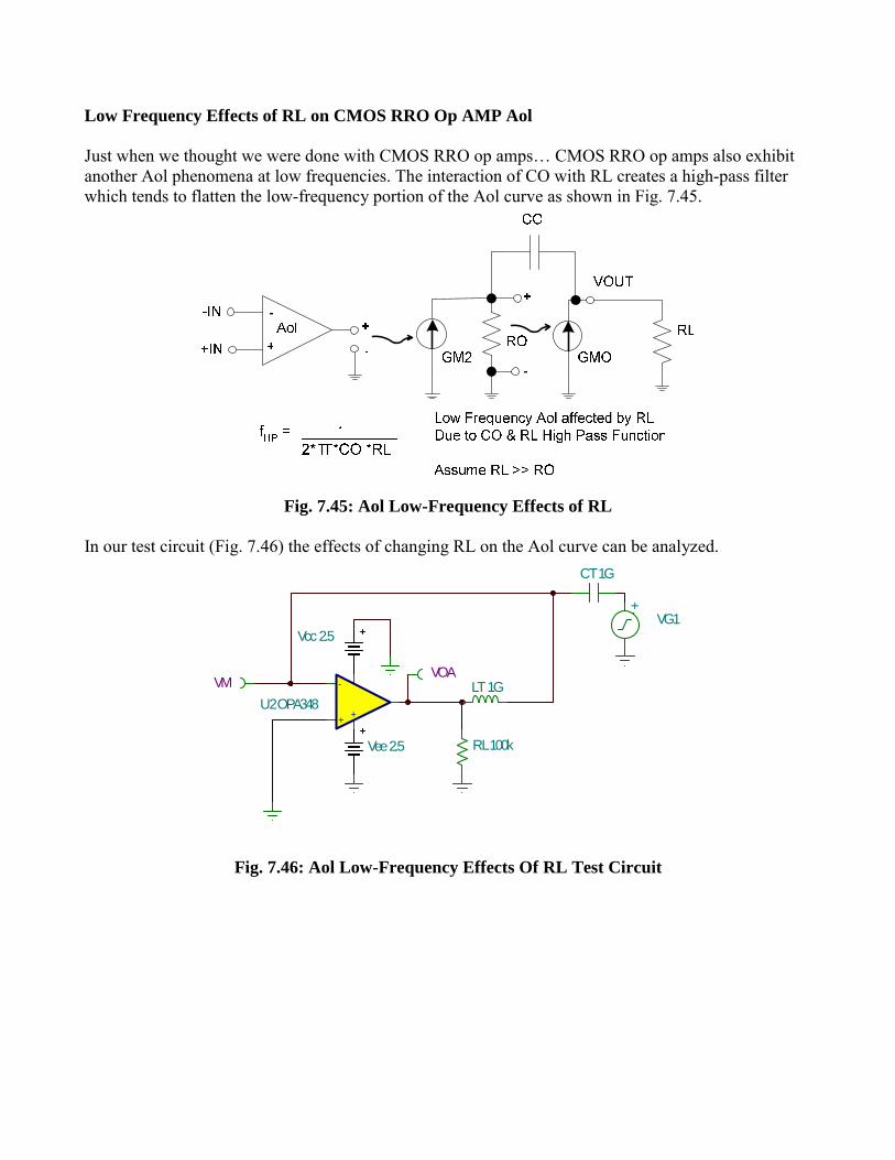
Low Frequency Effects of RL on CMOS RRO Op AMP Aol Just when we thought we were done with CMOS RRO op amps… CMOS RRO op amps also exhibit another Aol phenomena at low frequencies. The interaction of CO with RL creates a high-pass filter which tends to flatten the low-frequency portion of the Aol curve as shown in Fig. 7.45.
Fig. 7.45: Aol Low-Frequency Effects of RL In our test circuit (Fig. 7.46) the effects of changing RL on the Aol curve can be analyzed.
Vee 2.5
VOA
Vcc 2.5
+
-
+U2 OPA348
VM
+VG1
CT 1G
LT 1G
RL 100k
Fig. 7.46: Aol Low-Frequency Effects Of RL Test Circuit

Fig. 7.47 shows the low-frequency Aol effects due to resistive loading of no load, 100 kΩ and 5 kΩ. T
No Load
RL = 100k
RL = 5k
Frequency (Hz)1 10 100 1k 10k 100k 1M 10M
Gai
n (d
B)
-60.00
-40.00
-20.00
0.00
20.00
40.00
60.00
80.00
100.00
120.00
140.00
RL = 5k
RL = 100k
No Load
Fig. 7.47: Ac Plot Of RL Effects On Low-Frequency Portion Of Aol A clever test circuit (Fig. 7.48) will allow us to see clearly the effects of CO and RL on the low-frequency portion of the CMOS RRO Aol curve. Vaol represents the unloaded, unmodified Aol curve. VHP is the high-pass filter function created by CO and RL and VOA is the modified Aol curve caused by passing the unmodified Aol curve thought the filter.
+
-
+U1 OPA348
V1 2.5
V2 2.5RL 1
Vaol
+
VG1
CO 462n
RL 5k
VOA
L1 1G
CO' 462n
RL' 5k
VHP
Vaol = Equivalent of Aol + GM2 + RO
VOA = Equivalent of Op Amp Aol w/effect of RL
VHP = High Pass Filter Response of CO and RL
Fig. 7.48: Equivalent Circuit To Evaluate RL Effects On Aol

For RL = 5 kΩ our resultant ac curves (Fig. 7.49) show the unmodified Aol curve, Vaol, the high-pass filter effect due to CO and RL, and the net transfer function, modified Aol curve VOA due to passing Vaol through VHP. Since addition on a Bode plot is equivalent to linear multiplication we can easily add Vaol to VHP to see the resultant VOA curve.
T
VHP
VOA
Vaol
Frequency (Hz)1 10 100 1k 10k 100k 1M 10M
Gai
n (d
B)
-40.00
-20.00
0.00
20.00
40.00
60.00
80.00
100.00
120.00
VHP A:(2.01; -30.71) VOA A:(2.01; 77.44) Vaol A:(2.01; 108.15)
VHP
VOA
Vaol
a
Fig. 7.49: Equivalent Circuit Plots To Evaluate RL Effects On Aol

ZO Summary for CMOS RRO Op Amps Fig. 7.50 summarizes the key characteristics of ZO for CMOS RRO op amps. At high frequencies ZO is dominated by RO. For most loads, as dc output load current increases RO decreases making RO inversely proportional to IOUT. However, for low values of IOUT, RO is proportional to IOUT. ZO is capacitive, CO, at mid to low frequencies. If capacitive loads, CL, are connected to a CMOS RRO output then RO and CO will interact with CL to create a modified Aol curve which contains an additional pole, fp2, from the original Aol curve. The low-frequency portion of the Aol curve is affected by resistive loads, RL, interacting with CO, forming a high-pass filter and flattening the Aol curve in the mid- to low-frequency region. RO does change with process and temperature and a good rule-of-thumb including these changes is 0. 5*ROtyp at -55°C to 2*ROtyp at 125°C, where ROtyp is at 25°C. There are always exceptions to the rules-of-thumb we have developed for open-loop output impedance of CMOS RRO op amps. The most complete and accurate data for ZO should be obtained from the op amp manufacturer, or measured.
ZO is Dominated by RO at High FrequenciesRO is Inversely Proportional to IOUT for Most Values of IOUT
RO is Proportional to IOUT for Very Small Values of IOUT
ZO is Capacitive (CO) at Mid to Low FrequenciesRO, CO, and CL form a Second Pole to create a Modified AolRL and CO change the Low Frequency Portion of AolRO Change with Process and Temperature:
RO @ -55C = 0.5 * ROtyp (i.e. 50 ohms) RO @ 25C = ROtyp (i.e. 100 ohms) RO @ +125C = 2 * ROtyp (i.e. 200 ohms)
Use ROtyp for Stability Synthesis Decade Rules-of-Thumb will provide Design Margin
Fig. 7.50: ZO Summary For CMOS RRO
Acknowledgements A special thanks for all of the technical insights on ZO to the following individuals:
Burr-Brown Products from Texas Instruments Sergey Alenin, Senior Analog IC Design Engineer Tony Larson, Senior Analog IC Design Engineer Rod Burt, Senior Analog IC Design Manager
Analog & RF Models Bill Sands, Consultant. http://www.home.earthlink.net/%7Ewksands/

References Gray, Paul R and Meyer, Robert G. Analysis and Design of Analog Integrated Circuits. John Wiley & Sons. New York. 1977 Holt, Charles A Electronic Circuits. John Wiley & Sons. New York. 1978 About The Author After earning a BSEE from the University of Arizona, Tim Green has worked as an analog and mixed-signal board/system level design engineer for over 23 years, including brushless motor control, aircraft jet engine control, missile systems, power op amps, data acquisition systems, and CCD cameras. Tim's recent experience includes analog & mixed-signal semiconductor strategic marketing. He is currently the Linear Applications Engineering Manager at Burr-Brown, a division of Texas Instruments, in Tucson, AZ and focuses on instrumentation amplifiers and digitally-programmable analog conditioning ICs. He can be contacted at [email protected]