operational modes: mode basic input/output · the control words for both mode definition and bit...
TRANSCRIPT
Jntuhubupdates.com jntuhubupdates
PROGRAMMABLE PERIPHERAL INTERFACE 8255
The 8255 is a PPI which is used for parallel data T/f.
It has three 8-bit ports1. PORT A 2. PORT B 3. PORT C which are arranged in two groups.
It can be programmed to operate in three modes: Mode 0, Mode 1, Mode 2.
Each port has a unique address, and data can be read from or written to a port, by issuing either an IN or OUT instruction.
Operational Modes: Mode 0: Basic Input/output
In this mode, port A and port B can be configured as simple 8-bit input or output ports without handshaking.
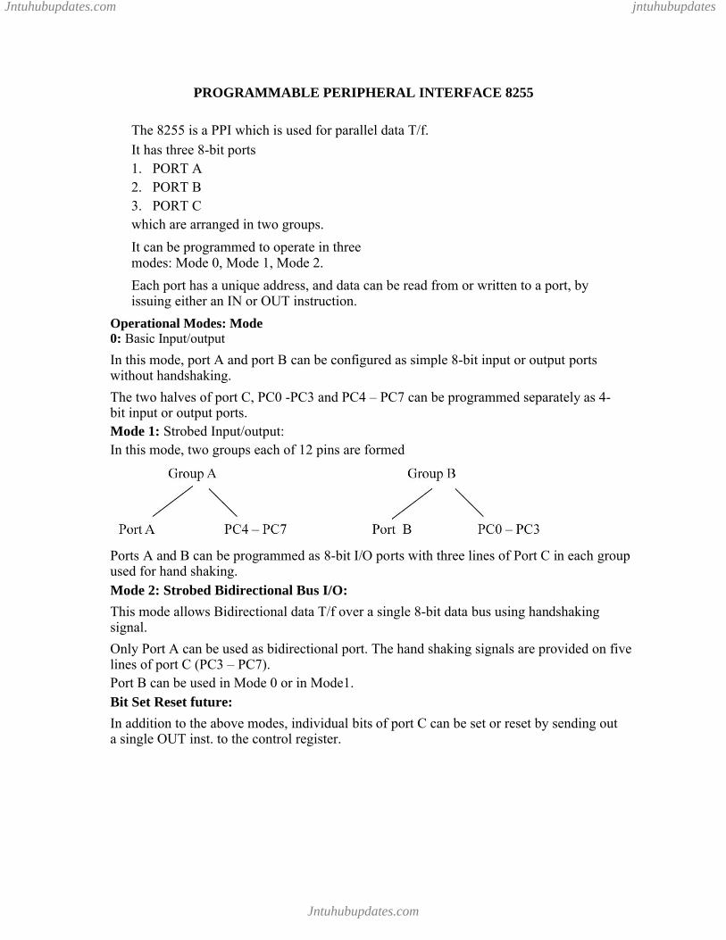
The two halves of port C, PC0 -PC3 and PC4 – PC7 can be programmed separately as 4-bit input or output ports.Mode 1: Strobed Input/output:In this mode, two groups each of 12 pins are formed
Ports A and B can be programmed as 8-bit I/O ports with three lines of Port C in each group used for hand shaking.Mode 2: Strobed Bidirectional Bus I/O:
This mode allows Bidirectional data T/f over a single 8-bit data bus using handshaking signal.
Only Port A can be used as bidirectional port. The hand shaking signals are provided on five lines of port C (PC3 – PC7).Port B can be used in Mode 0 or in Mode1.Bit Set Reset future:
In addition to the above modes, individual bits of port C can be set or reset by sending out a single OUT inst. to the control register.
Jntuhubupdates.com
Jntuhubupdates.com jntuhubupdates
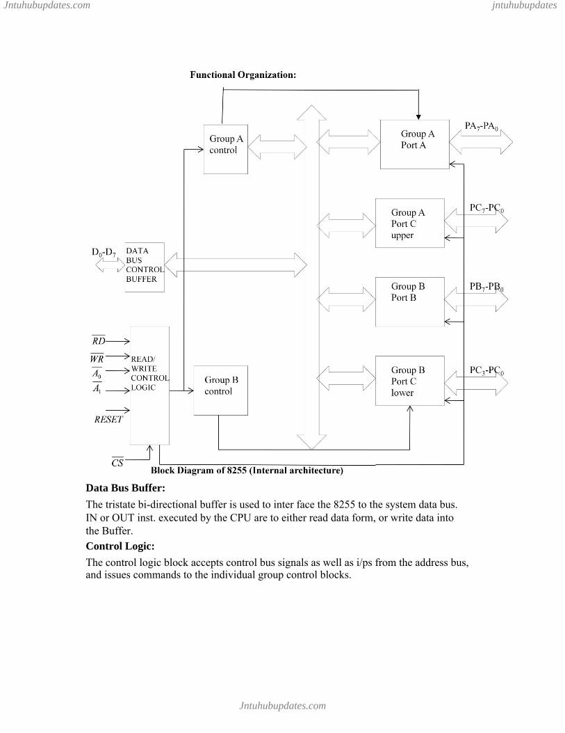
Data Bus Buffer:
The tristate bi-directional buffer is used to inter face the 8255 to the system data bus. IN or OUT inst. executed by the CPU are to either read data form, or write data into the Buffer.
Control Logic:
The control logic block accepts control bus signals as well as i/ps from the address bus, and issues commands to the individual group control blocks.
Jntuhubupdates.com
Jntuhubupdates.com jntuhubupdates
Group A and Group B controls:
Each of the group A and group B control Blocks receivers control words from the CPU through the data Buffer and internal data bus, accepts commands from control block, and issues appropriate commands to the ports associated with it.
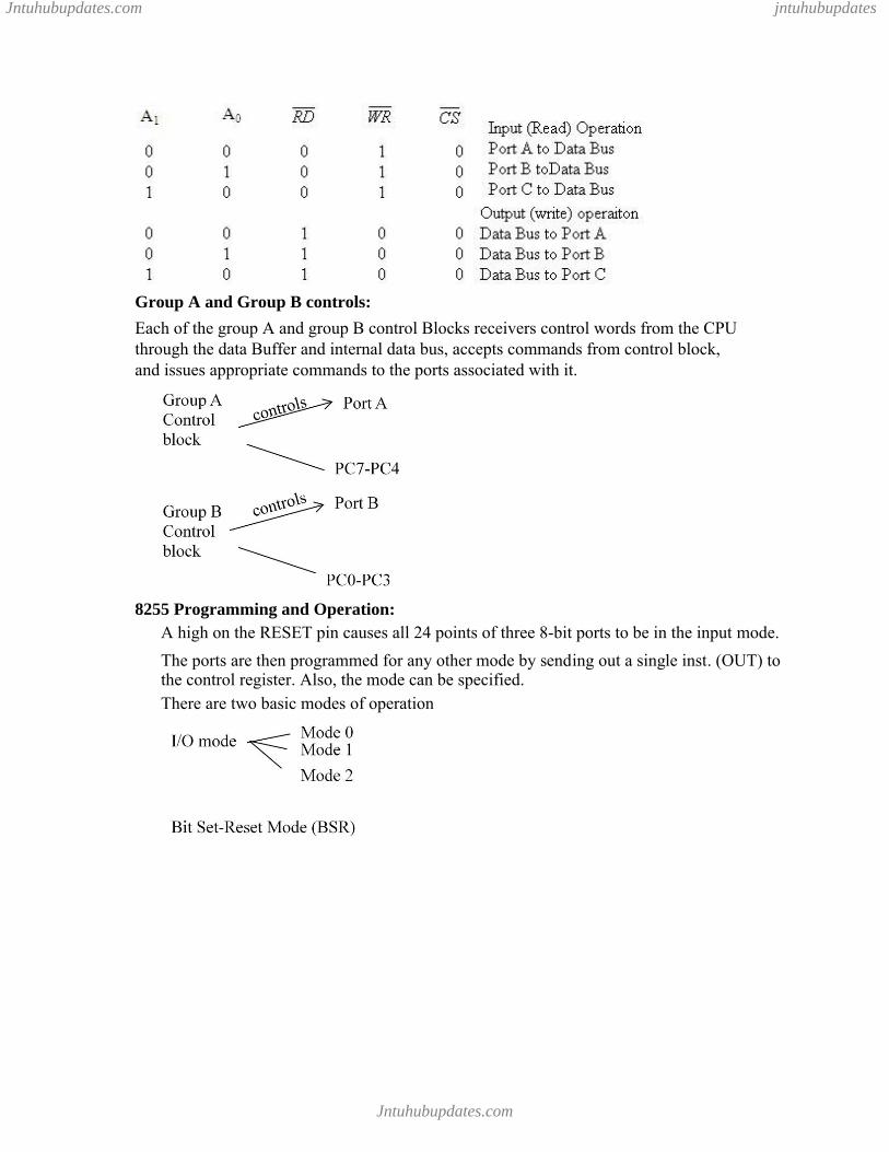
8255 Programming and Operation:A high on the RESET pin causes all 24 points of three 8-bit ports to be in the input mode.
The ports are then programmed for any other mode by sending out a single inst. (OUT) to the control register. Also, the mode can be specified.There are two basic modes of operation
Jntuhubupdates.com

Jntuhubupdates.com jntuhubupdates
Bit set/Reset format Control word
Jntuhubupdates.com

Jntuhubupdates.com jntuhubupdates
The control words for both mode definition and Bit Set-reset are loaded into the same control register with bit D7 for specifying whether it is mode definition word or Bit set-Reset word.
Example for BSR Mode:If bit PC2 is to be set, then control reg. would be 0XXX0101If bit PC7 is to be Reset, then control reg. would be 0XXX1110.
8255 PROGRAMMING
Mode 0:
In the control word, D7 is set to 1.D6, D5, D2: 0 [to configure all the ports in Mode 0]D4, D3, D1, D0: determine whether the corresponding ports are configured as I/P or O/P For example, If Port A, Port B: I/P ports : D4=1
D1=1PCL: O/P: D0=0PCU: I/P: D3=1
Jntuhubupdates.com

Jntuhubupdates.com jntuhubupdates
Mode 1: ( Strobed input/output mode )In this mode the handshaking control the input and output action of the specified port.
Port C lines PC0-PC2, provide strobe or handshake lines for port B. This group which includes port B and PC0-PC2 is called as group B for Strobed datainput/output. Port C lines PC3-PC5 provides strobe lines for port A. This group including port A and PC3-PC5 from group A. Thus port C is utilized for generating handshake signals.
Two groups – group A and group B are available for strobed data transfer. Each group contains one 8-bit data I/O port and one 4-bit control/data port. The 8-bit data port can be either used as input and output port. The inputs and outputs both are latched. Out of 8-bit port C, PC0-PC2 are used to generate control signals for port B and PC3-PC5 are used to generate control signals for port A. the lines PC6, PC7 may be used as independent data lines.
The control signals for both the groups in input and output modes are explained as follows:Input control signal definitions (mode 1 ):STB( Strobe input ) – If this lines falls to logic low level, the data available at 8-bit input port isloaded into input latches.IBF ( Input buffer full ) – If this signal rises to logic 1, it indicates that data has been loadedinto latches, i.e. it works as an acknowledgement. IBF is set by a low on STB and is reset by the rising edge of RD input.INTR ( Interrupt request ) – This active high output signal can be used to interrupt the CPUwhenever an input device requests the service. INTR is set by a high STB pin and a high at IBF pin. INTE is an internal flag that can be controlled by the bit set/reset mode of either PC4(INTEA) or PC2(INTEB) as shown in fig.Output control signal definitions (mode 1) :OBF (Output buffer full) – This status signal, whenever falls to low, indicates that CPU haswritten data to the specified output port. The OBF flip-flop will be set by arising edge of WR signal and reset by a low going edge at the ACK input.ACK ( Acknowledge input ) – ACK signal acts as an acknowledgement to be given by anoutput device. ACK signal, whenever low, informs the CPU that the data transferred by the CPU to the output device through the port is received by the output device.INTR ( Interrupt request ) – Thus an output signal that can be used to interrupt the CPU whenan output device acknowledges the data received from the CPU. INTR is set when ACK, OBF and INTE are 1. It is reset by a falling edge on WR input. The INTEA and INTEB flags are controlled by the bit set-reset mode of PC6 and PC2 respectively.
Jntuhubupdates.com

Jntuhubupdates.com jntuhubupdates
Jntuhubupdates.com

Jntuhubupdates.com jntuhubupdates
Jntuhubupdates.com

Jntuhubupdates.com jntuhubupdates
Mode 2 ( Strobed bidirectional I/O ): This mode of operation of 8255 is also called as strobedbidirectional I/O. This mode of operation provides 8255 with an additional features for communicating with a peripheral device on an 8-bit data bus. Handshaking signals are provided to maintain proper data flow and synchronizationbetween the data transmitter and receiver. The interrupt generation and other functions are similar to mode 1.
Control signal definitions in mode 2:
INTR – (Interrupt request) As in mode 1, this control signal is active high and is used tointerrupt the microprocessor to ask for transfer of the next data byte to/from it. This signal is used for input ( read ) as well as output ( write ) operations.Control Signals for Output operations:OBF ( Output buffer full ) – This signal, when falls to low level, indicates that the CPU haswritten data to port A.ACK ( Acknowledge ) This control input, when falls to logic low level, acknowledges that theprevious data byte is received by the destination and next byte may be sent by the processor. This signal enables the internal tristate buffers to send the next data byte on port A.INTE1 ( A flag associated with OBF ) This can be controlled by bit set/reset mode with PC6.
Jntuhubupdates.com
Jntuhubupdates.com jntuhubupdates
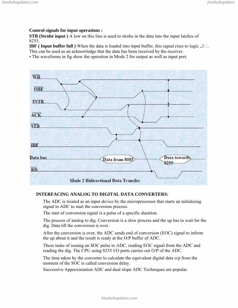
Control signals for input operations :STB (Strobe input ) A low on this line is used to strobe in the data into the input latches of8255.IBF ( Input buffer full ) When the data is loaded into input buffer, this signal rises to logic „1�.This can be used as an acknowledge that the data has been received by the receiver.• The waveforms in fig show the operation in Mode 2 for output as well as input port.
INTERFACING ANALOG TO DIGITAL DATA CONVERTERS:
The ADC is treated as an input device by the microprocessor that starts an initializing signal to ADC to start the conversion process.
The start of conversion signal is a pulse of a specific duration.
The process of analog to dig. Conversion is a slow process and the up has to wait for the dig. Data till the conversion is over.
After the conversion is over, the ADC sends end of conversion (EOC) signal to inform the up about it and the result is ready at the O/P buffer of ADC.
These tasks of issuing an SOC pulse to ADC, reading EOC signal from the ADC and reading the dig. The CPU using 8255 I/O ports carries out O/P of the ADC.
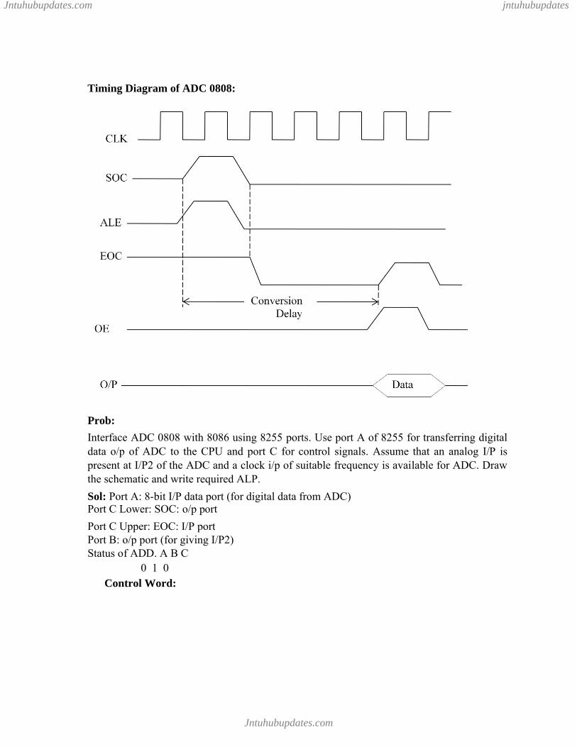
The time taken by the converter to calculate the equivalent digital data o/p from the moment of the SOC is called conversion delay.Successive Approximation ADC and dual slope ADC Techniques are popular.
Jntuhubupdates.com
Jntuhubupdates.com jntuhubupdates
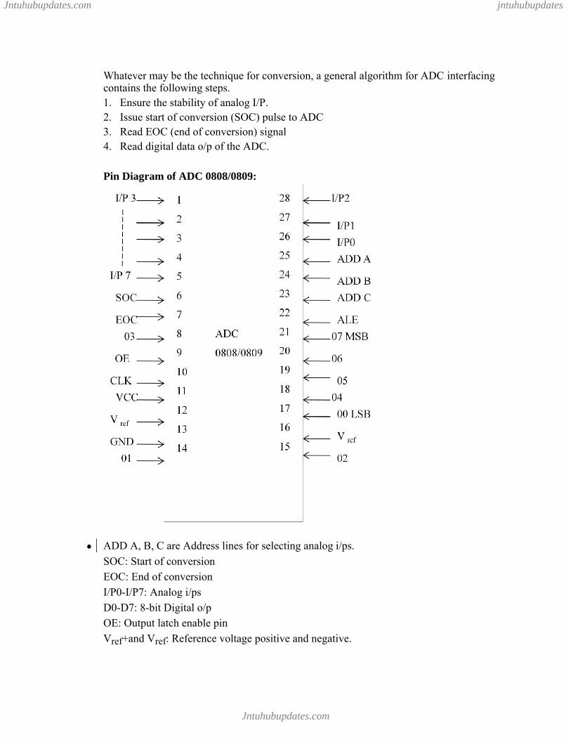
Whatever may be the technique for conversion, a general algorithm for ADC interfacing contains the following steps.1. Ensure the stability of analog I/P. 2. Issue start of conversion (SOC) pulse to ADC 3. Read EOC (end of conversion) signal 4. Read digital data o/p of the ADC.
Pin Diagram of ADC 0808/0809:
ADD A, B, C are Address lines for selecting analog i/ps.
SOC: Start of conversion
EOC: End of conversion
I/P0-I/P7: Analog i/ps
D0-D7: 8-bit Digital o/p
OE: Output latch enable pin
Vref+and Vref: Reference voltage positive and negative.
Jntuhubupdates.com
Jntuhubupdates.com jntuhubupdates
Timing Diagram of ADC 0808:
Prob:
Interface ADC 0808 with 8086 using 8255 ports. Use port A of 8255 for transferring digital data o/p of ADC to the CPU and port C for control signals. Assume that an analog I/P is present at I/P2 of the ADC and a clock i/p of suitable frequency is available for ADC. Draw the schematic and write required ALP.
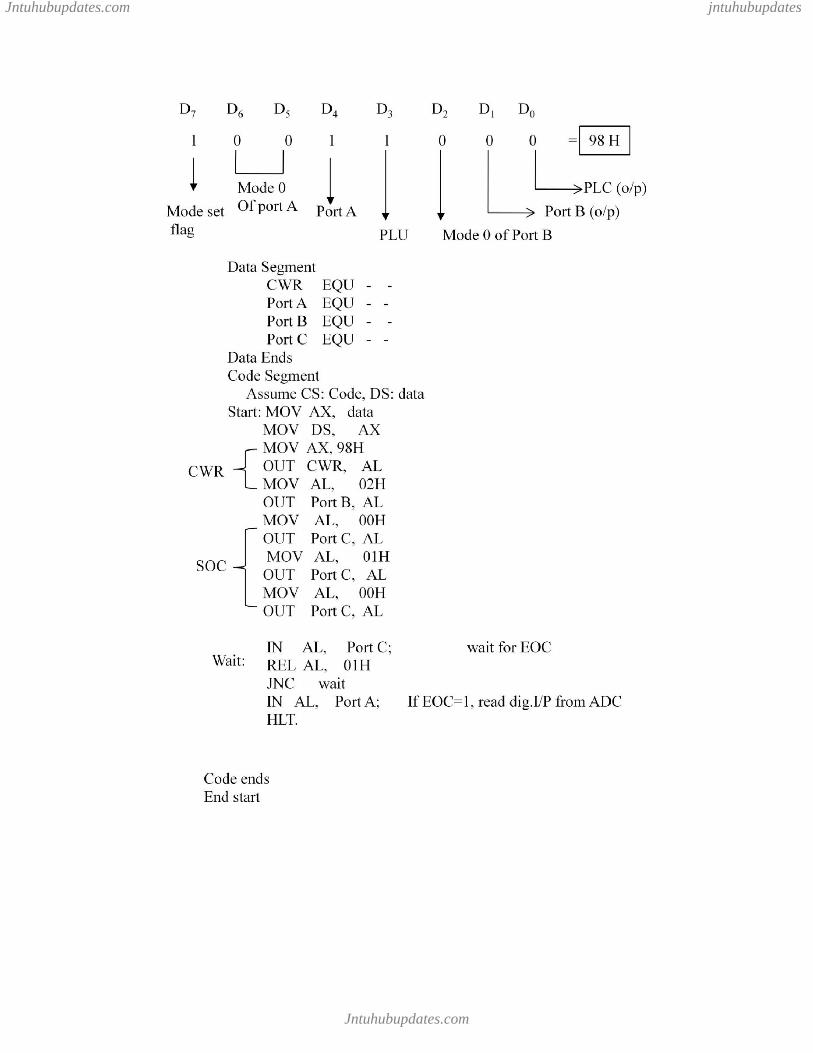
Sol: Port A: 8-bit I/P data port (for digital data from ADC)Port C Lower: SOC: o/p port
Port C Upper: EOC: I/P port Port B: o/p port (for giving I/P2) Status of ADD. A B C
0 1 0Control Word:
Jntuhubupdates.com
Jntuhubupdates.com jntuhubupdates
Jntuhubupdates.com
Jntuhubupdates.com jntuhubupdates
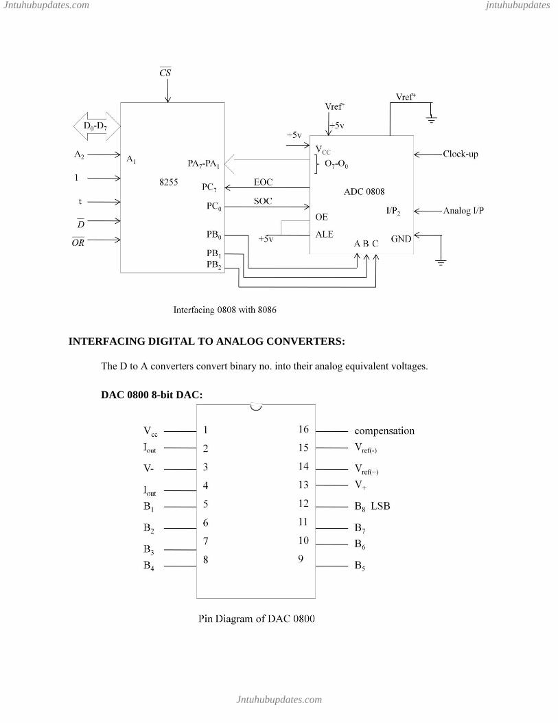
INTERFACING DIGITAL TO ANALOG CONVERTERS:
The D to A converters convert binary no. into their analog equivalent voltages.
DAC 0800 8-bit DAC:
Jntuhubupdates.com

Jntuhubupdates.com jntuhubupdates
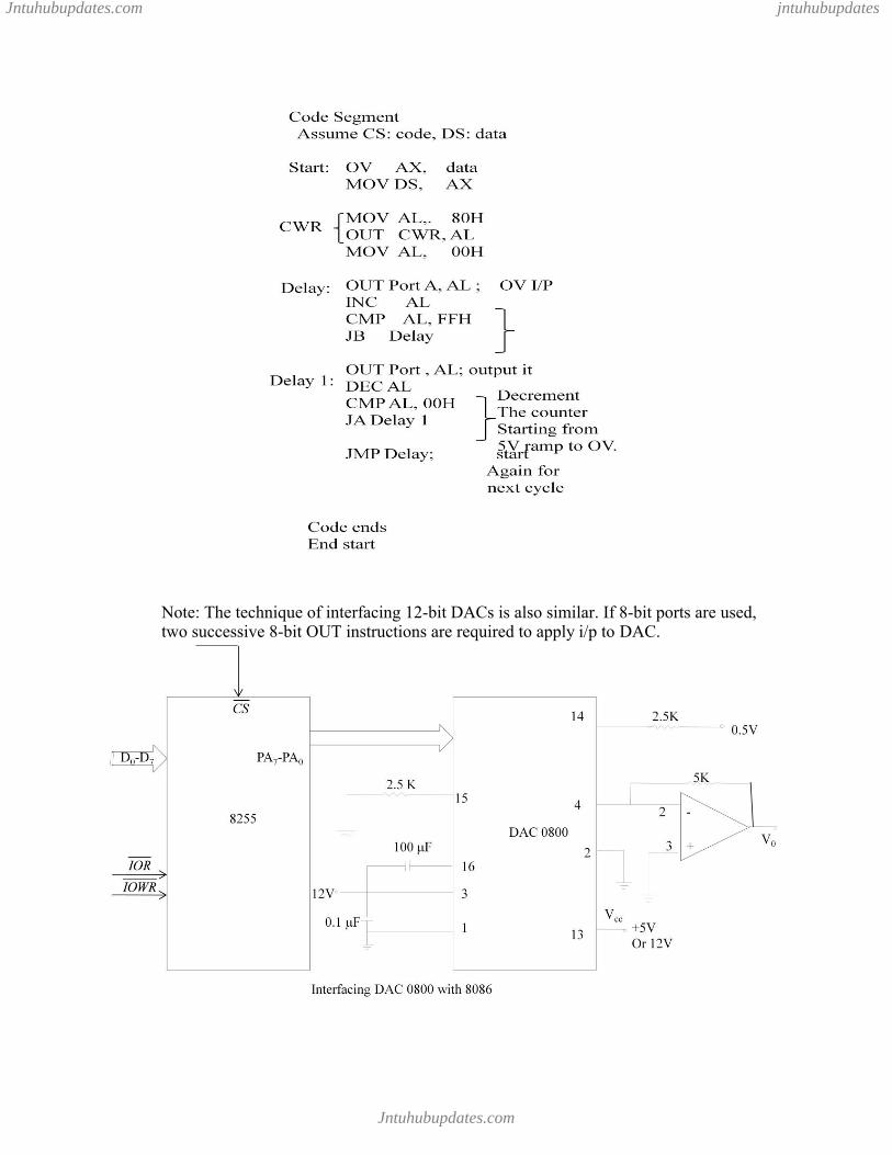
Problem:Write an ALP to generate a triangular wave of frequency 500 Hz using the interfacing ckt shown in fig. below. The 8086 system operates at 8MHz. The amplitude of the triangular wave should be +5V.
Sol:Port A: o/p Digital data to DAC.Only port A is used, so the remaining ports are configured as o/ps.
Jntuhubupdates.com
Jntuhubupdates.com jntuhubupdates
Note: The technique of interfacing 12-bit DACs is also similar. If 8-bit ports are used, two successive 8-bit OUT instructions are required to apply i/p to DAC.
Jntuhubupdates.com
Jntuhubupdates.com jntuhubupdates
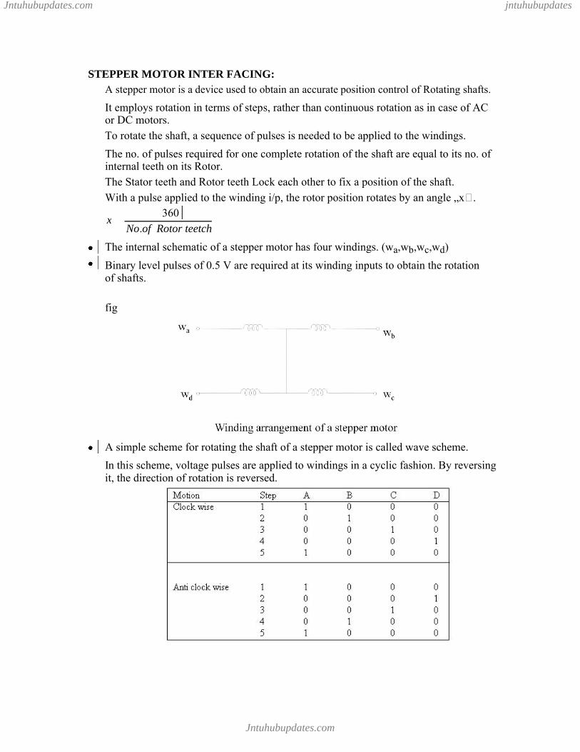
STEPPER MOTOR INTER FACING:A stepper motor is a device used to obtain an accurate position control of Rotating shafts.
It employs rotation in terms of steps, rather than continuous rotation as in case of AC or DC motors.
To rotate the shaft, a sequence of pulses is needed to be applied to the windings.
The no. of pulses required for one complete rotation of the shaft are equal to its no. of internal teeth on its Rotor.
The Stator teeth and Rotor teeth Lock each other to fix a position of the shaft.
With a pulse applied to the winding i/p, the rotor position rotates by an angle „x�.
x360
No.of Rotor teetch
The internal schematic of a stepper motor has four windings. (wa,wb,wc,wd)
Binary level pulses of 0.5 V are required at its winding inputs to obtain the rotation of shafts.
fig
A simple scheme for rotating the shaft of a stepper motor is called wave scheme.
In this scheme, voltage pulses are applied to windings in a cyclic fashion. By reversing it, the direction of rotation is reversed.
Jntuhubupdates.com

Jntuhubupdates.com jntuhubupdates
Another scheme of stepper motor applies two pulses to two successive windings at a time.
Problem: Design a stepper motor and write an ALP to rotate shaft of 4-phase stepper motor.i) in clock wise 5 rotations ii) in Anti clock wise 5 rotations
The port A address is 0740H. The stepper motor has 200 rotor teeth. The port A0 drives winding wa, PA1 drives winding wb and soon. It has an internal delay of 10 msec.
Sol: Data segmentCWR EQU - - -Port A EQU 0740 HData EndsCode SegmentAssume CS: code, DS: dataStart: MOV AX, data
MOV DS, AXMOV AL, 88 H; Bit pattern 10001000 to startMOV CX, 1000; 200 Rotor teeth.
No. of Rotation * teeth = countCount = 200*5
=
L1: OUT Port A, ALCALL DelayROR AL, 01
Jntuhubupdates.com

Jntuhubupdates.com jntuhubupdates
DEC CXJNZ L1MOV AH, 88 H, MOV CX, 1000
L2= OUT Port A, AHCALL DELAYROL AH, 01DEC CXJNZ L2HLT
Code EndsEnd Start
Code 1 SegmentDelay PROC FARAssume CS: code 1, DS: DataHERE: MOV CX, OFFF H
LOOP HEREDelay ENDPCode 1 ends
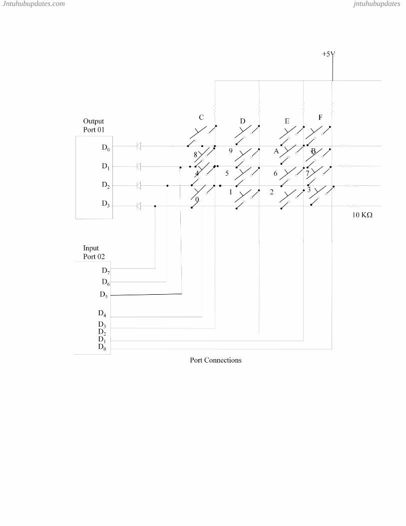
KEY BOARD INTER FACING:Pressing a key is nothing but activating a switch. There are many types of switches.
Mechanical key switches
Membrane key switches
Capacitive key switches
Hall effect key switches
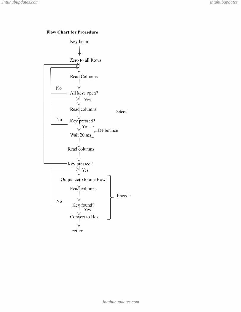
In most key boards, the key switches are connected in a matrix of Rows and Columns. We will use simple mechanical switches here, but the principle is same for all the switches.Process:1. Detect a key press. 2. De bounce the key press 3. Encode the key press.
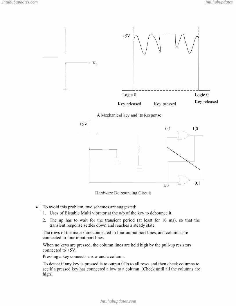
A Logic „0� is read by the micro processor when the key is pressed.Key De bounce:
Whenever a mechanical push-button is pressed or released once, the mechanical components of the key do not change the position smoothly, rather it generates a transient response as shown in fig. These may be interpreted as the multiple key pressures and responded accordingly.
Jntuhubupdates.com
Jntuhubupdates.com jntuhubupdates
To avoid this problem, two schemes are suggested:1. Uses of Bistable Multi vibrator at the o/p of the key to debounce it.
2. The up has to wait for the transient period (at least for 10 ms), so that the transient response settles down and reaches a steady state
The rows of the matrix are connected to four output port lines, and columns are connected to four input port lines.
When no keys are pressed, the column lines are held high by the pull-up resistors connected to +5V.Pressing a key connects a row and a column.
To detect if any key is pressed is to output 0�s to all rows and then check columns to see if a pressed key has connected a low to a column. (Check until all the columns are high).
Jntuhubupdates.com

Jntuhubupdates.com jntuhubupdates
Once the columns are found to be all high, the program enters another loop, which waits until a low appears on one of the columns. (Indicating a key press).For this a simple 20 m.s delay is executed to de bounce task.
After the de bounce time, another check is made to see if the key is still pressed. If the columns are now all high, then no key is pressed and the initial detection was caused by a Noise pulse.
Jntuhubupdates.com
Jntuhubupdates.com jntuhubupdates
If any of the columns are low now, then the assumption is made that it was a valid key press.
The final task is to determine the row and column of the pressed key and convert this inf. to hex code for the pressed key.
For this, a low is given to rows and now column is read.
If none of the columns is low, the pressed key is not in that row, so the low is rotated to next row and repeat again.This is repeated until a low on a row produces a low on one of the columns.
Therefore, the 4-bit code from i/p port (ROW) and the 4-bit code from o/p port (column) are converted to Hex code.
This ENCODE portion uses a compare technique. This is done with the LOOK UP table containing 8-bit key pressed codes for 16-keys.
Jntuhubupdates.com
Jntuhubupdates.com jntuhubupdates
Jntuhubupdates.com
Jntuhubupdates.com jntuhubupdates
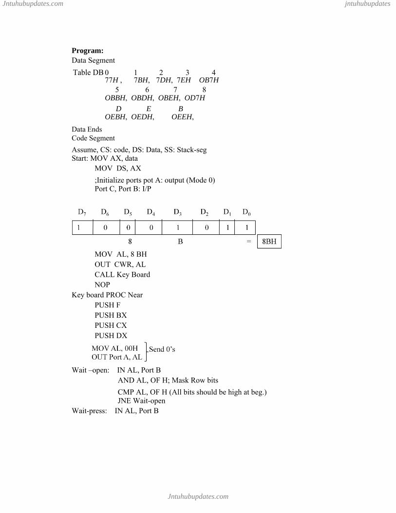
Program:Data Segment
Table DB 0 1 2 3 477H , 7BH, 7DH, 7EH OB7H
5 6 7 8OBBH, OBDH, OBEH, OD7H
D E BOEBH, OEDH, OEEH,
Data Ends Code Segment
Assume, CS: code, DS: Data, SS: Stack-seg Start: MOV AX, data
MOV DS, AX
;Initialize ports pot A: output (Mode 0) Port C, Port B: I/P
MOV AL, 8 BHOUT CWR, ALCALL Key BoardNOP
Key board PROC NearPUSH FPUSH BXPUSH CXPUSH DX
Wait –open: IN AL, Port BAND AL, OF H; Mask Row bits
CMP AL, OF H (All bits should be high at beg.) JNE Wait-open
Wait-press: IN AL, Port B
Jntuhubupdates.com

Jntuhubupdates.com jntuhubupdates
Jntuhubupdates.com
Jntuhubupdates.com jntuhubupdates
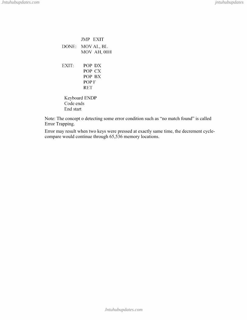
Note: The concept o detecting some error condition such as “no match found” is called Error Trapping.
Error may result when two keys were pressed at exactly same time, the decrement cycle-compare would continue through 65,536 memory locations.
Jntuhubupdates.com
Jntuhubupdates.com jntuhubupdates