opsp hardware manual
TRANSCRIPT

REJ09B0134-0100Z
Rev.1.00 Revision date : Mar 01,2004
32
RENESAS 32-BIT OPEN PLATFORM SYNTHESIZABLE PROCESSOR
OPSPHardware Manual

Keep safety first in your circuit designs!
Notes regarding these materials
1. Renesas Technology Corporation puts the maximum effort into making semiconductor prod-ucts better and more reliable, but there is always the possibility that trouble may occur withthem. Trouble with semiconductors may lead to personal injury, fire or property damage.Remember to give due consideration to safety when making your circuit designs, with ap-propriate measures such as (i) placement of substitutive, auxiliary circuits, (ii) use of non-flammable material or (iii) prevention against any malfunction or mishap.
1. These materials are intended as a reference to assist our customers in the selection of theRenesas Technology Corporation product best suited to the customer's application; they donot convey any license under any intellectual property rights, or any other rights, belongingto Renesas Technology Corporation or a third party.
2. Renesas Technology Corporation assumes no responsibility for any damage, or infringe-ment of any third-party's rights, originating in the use of any product data, diagrams, charts,programs, algorithms, or circuit application examples contained in these materials.
3. All information contained in these materials, including product data, diagrams, charts, pro-grams and algorithms represents information on products at the time of publication of thesematerials, and are subject to change by Renesas Technology Corporation without noticedue to product improvements or other reasons. It is therefore recommended that custom-ers contact Renesas Technology Corporation or an authorized Renesas Technology Cor-poration product distributor for the latest product information before purchasing a productlisted herein.The information described here may contain technical inaccuracies or typographical errors.Renesas Technology Corporation assumes no responsibility for any damage, liability, orother loss rising from these inaccuracies or errors.Please also pay attention to information published by Renesas Technology Corporation byvarious means, including the Renesas Technology Corporation Semiconductor home page(http://www.renesas.com).
4. When using any or all of the information contained in these materials, including productdata, diagrams, charts, programs, and algorithms, please be sure to evaluate all informa-tion as a total system before making a final decision on the applicability of the informationand products. Renesas Technology Corporation assumes no responsibility for any dam-age, liability or other loss resulting from the information contained herein.
5. Renesas Technology Corporation semiconductors are not designed or manufactured foruse in a device or system that is used under circumstances in which human life is poten-tially at stake. Please contact Renesas Technology Corporation or an authorized RenesasTechnology Corporation product distributor when considering the use of a product con-tained herein for any specific purposes, such as apparatus or systems for transportation,vehicular, medical, aerospace, nuclear, or undersea repeater use.
6. The prior written approval of Renesas Technology Corporation is necessary to reprint orreproduce in whole or in part these materials.
7. If these products or technologies are subject to the Japanese export control restrictions,they must be exported under a license from the Japanese government and cannot be im-ported into a country other than the approved destination.Any diversion or reexport contrary to the export control laws and regulations of Japan and/or the country of destination is prohibited.
8. Please contact Renesas Technology Corporation for further details on these materials orthe products contained therein.

REVISION HISTORY OPSP Hardware Manual
Description Rev. Date Page Summary
1.00 Mar 01,2004 - First edition issued

Guide to Understanding the Register Table (1) Bit number : Indicates a register's bit number. (2) Access data size : The data size which can be accessed to the register is indicated. (3) Status after reset : The initial state of each register after reset is indicated in hexadecimal or binary. (4) Status after reset : The initial state of each register after reset is indicated bitwise.
0 : This bit is "0" after reset. 1 : This bit is "1" after reset. ? : This bit is undefined after reset.
(5) Read conditions : R : This bit can be accessed of read. ? : The value read from this bit is undefined. (Reading this bit has no effect.) 0 : The value read from this bit is always "0". 1 : The value read from this bit is always "1".
(6) Write conditions : W : This bit can be accessed for write. N : This bit is write protected. 0 : To write to this bit, always write "0". 1 : To write to this bit, always write "1". Note : Care must be taken when writing to this bit. See Note in each register table.
DMA Transfer Enable Register (DMAEN) <Address: H’00EF 8000>
b0 1 2 3 4 5 6 7 8 9 10 11 12 13 14 b15
0 0 0 0 0 0 0 0 0 0 0 0 0 0 0 0
b16 17 18 19 20 21 22 23 24 25 26 27 28 29 30 b31
DMSK0 DMSK1 DEN0 DEN1 0 0 0 0 0 0 0 0 0 0 0 0 0 0 0 0
* This register can be accessed bytewise (in 8 bits), halfwordwise (in 16 bits) or wordwise (in 32 bits)
<After reset: H’0000 0000>
b Bit Name Function R W
0–15 No functions assigned. Fix these bits to 0. 0 0 16 DMSK0
DEN0 write mask bit 0 : Write to DEN0 masked 1 : Write to DEN0 unmasked
0 Note
17 DMSK1 DMA1 transfer enable bit
0 : Disable DMA transfer on DMA1 1 : Enable DMA transfer on DMA1
0 Note
18–23 No functions assigned. Fix these bits to 0. 0 0 24 DEN0
DMA0 transfer enable bit 0 : Disable DMA transfer on DMA0 1 : Enable DMA transfer on DMA0
R W
25 DEN1 DMA1 transfer enable bit
0 : Disable DMA transfer on DMA1 1 : Enable DMA transfer on DMA1
R W
26–31 No functions assigned. Fix these bits to 0. 0 0 Note: This means that writing data “0” has no effect, and that data “1” written to the bit is not retained.
(1)
(2)
(3)
(4)
(5) (6)
Rev.1.00 Mar 05,2004 (1)
REJ09B0134-0100Z
Table of contents
CHAPTER 1 OVERVIEW
1.1 OPSP Overview ........................................................................................................................................................ 1-2 1.1.1 OPSP-CPU...................................................................................................................................................... 1-2 1.1.2 Memory Management Function ..................................................................................................................... 1-4 1.1.3 Built-in SRAM and Caches............................................................................................................................ 1-4 1.1.4 Bi-endian Mechanism ..................................................................................................................................... 1-4 1.1.5 On-chip User IP Bus ..................................................................................................................................... 1-4 1.1.6 Clock ............................................................................................................................................................... 1-4 1.1.7 Powerful Peripheral Functions ....................................................................................................................... 1-5
1.2 Block Diagram........................................................................................................................................................... 1-6 1.3 Features..................................................................................................................................................................... 1-7
1.3.1 Features of the OPSP-CPU .......................................................................................................................... 1-7 1.3.2 Features of the Internal Memory .................................................................................................................. 1-7 1.3.3 Features of the Internal Peripheral I/O......................................................................................................... 1-8
1.4 Pin Functions .......................................................................................................................................................... 1-10
CHAPTER 2 THE CPU............................................................................................................................................ 1
2.1 Processor Modes ...................................................................................................................................................... 2-2 2.1.1 Privileged Instructions..................................................................................................................................... 2-2
2.2 CPU Registers .......................................................................................................................................................... 2-2 2.3 General-purpose Registers ....................................................................................................................................... 2-2 2.4 Control Registers ...................................................................................................................................................... 2-3
2.4.1 Processor Status Word Register: PSW (CR0)............................................................................................. 2-4 2.4.2 Condition Bit Register: CBR (CR1)............................................................................................................... 2-5 2.4.3 Stack Pointer for Interrupt: SPI (CR2) and Stack Pointer for User: SPU (CR3) ..................................... 2-5 2.4.4 EIT Vector Base Register: EVB (CR5) ........................................................................................................ 2-6 2.4.5 Backup PC: BPC (CR6) ................................................................................................................................ 2-6
2.5 Accumulators ............................................................................................................................................................. 2-7 2.6 Program Counter (PC) ............................................................................................................................................. 2-7 2.7 Data Formats ............................................................................................................................................................ 2-8
2.7.1 Bi-endian Function.......................................................................................................................................... 2-8 2.7.2 Data Types ..................................................................................................................................................... 2-8 2.7.3 Data Formats .................................................................................................................................................. 2-9
CHAPTER 3 ADDRESS SPACE
3.1 Physical Address Space........................................................................................................................................... 3-2 3.1.1 Outline of the Physical Address Space........................................................................................................ 3-2 3.1.2 Internal Space................................................................................................................................................. 3-3 3.1.3 Internal RAM Area ......................................................................................................................................... 3-3 3.1.4 SFR (Special Function Register) Area ......................................................................................................... 3-4
3.2 Operating Modes....................................................................................................................................................... 3-5

Rev.1.00 Mar 05,2004 (2)
REJ09B0134-0100Z
3.2.1 Processor Modes............................................................................................................................................ 3-5 3.2.2 Privileged Instructions..................................................................................................................................... 3-5
3.3 Virtual Address Space.............................................................................................................................................. 3-6 3.3.1 Address Translation Mode ............................................................................................................................. 3-6 3.3.2 Virtual Address Space in Supervisor Mode ................................................................................................. 3-6 3.3.3 Virtual Address Space in User Mode........................................................................................................... 3-9 3.3.4 Multiple Virtual Spaces................................................................................................................................. 3-12 3.3.5 Storage Protection ........................................................................................................................................ 3-12
CHAPTER 4 MEMORY MANAGEMENT UNIT (MMU)
4.1 Outline of the Memory Management Unit .............................................................................................................. 4-2 4.2 TLB Address Translation Method ............................................................................................................................ 4-2
4.2.1 TLB Address Translation................................................................................................................................ 4-2 4.2.2 Structure of the TLB ...................................................................................................................................... 4-3 4.2.3 Page Numbers and Addresses ..................................................................................................................... 4-4
4.3 TLB Entry Related Registers ................................................................................................................................... 4-5 4.3.1 Instruction TLB Entry Tag Registers............................................................................................................. 4-6 4.3.2 Instruction TLB Entry Data Registers ........................................................................................................... 4-7 4.3.3 Data TLB Entry Tag Registers...................................................................................................................... 4-9 4.3.4 Data TLB Entry Data Registers .................................................................................................................. 4-10
4.4 MMU Registers ....................................................................................................................................................... 4-12 4.4.1 Address Translation Mode Register ............................................................................................................ 4-13 4.4.2 MMU Page Size Specification Register ...................................................................................................... 4-14 4.4.3 MMU Address Space ID Register............................................................................................................... 4-15 4.4.4 MMU Exception Status Register ................................................................................................................. 4-16 4.4.5 Data MMU Exception Address Register ..................................................................................................... 4-18 4.4.6 Data MMU Exception Page Register.......................................................................................................... 4-19 4.4.7 TLB Search Virtual Address Register ......................................................................................................... 4-20 4.4.8 TLB Operation Register ............................................................................................................................... 4-21 4.4.9 Instruction TLB Index Register .................................................................................................................... 4-23 4.4.10 Data TLB Index Register ........................................................................................................................... 4-25
4.5 MMU Exception Handling....................................................................................................................................... 4-27 4.5.1 TLB Miss Exception (TME).......................................................................................................................... 4-27 4.5.2 Access Exception (ACE).............................................................................................................................. 4-27
4.6 Notes about the Memory Management Unit ........................................................................................................ 4-28 4.6.1 Precautions to Be Observed when Setting TLB Entries and MMU Control Registers........................... 4-28
CHAPTER 5 INTERNAL MEMORY
5.1 Outline of the Internal Memory ............................................................................................................................... 5-2 5.2 Internal Memory and the CPU Bus ........................................................................................................................ 5-2 5.3 Internal SRAM........................................................................................................................................................... 5-2 5.4 Caches....................................................................................................................................................................... 5-3
5.4.1 Cache Structure.............................................................................................................................................. 5-3 5.5 Cache Related Registers........................................................................................................................................ 5-6
Cache Related Register Mapping ........................................................................................................................... 5-6

Rev.1.00 Mar 05,2004 (3)
REJ09B0134-0100Z
5.5.1 Instruction Cache Area Control Register ...................................................................................................... 5-7 5.5.2 Data Cache Area Control Registe ................................................................................................................ 5-9 5.5.3 Cache Control Register................................................................................................................................ 5-11
5.6 Cache Operation..................................................................................................................................................... 5-14 5.6.1 Operation of the Instruction Cache............................................................................................................. 5-14 5.6.2 Operation of the Data Cache...................................................................................................................... 5-15
CHAPTER 6 EIT
6.1 Outline of EIT ........................................................................................................................................................... 6-2 6.2 EIT Events in the OPSP ......................................................................................................................................... 6-3
6.2.1 Exception......................................................................................................................................................... 6-3 6.2.2 Interrupt ........................................................................................................................................................... 6-4 6.2.3 Trap ................................................................................................................................................................. 6-4
6.3 EIT Processing Procedure ....................................................................................................................................... 6-5 6.4 EIT Processing Mechanism...................................................................................................................................... 6-7 6.5 Acceptance of EIT Events ....................................................................................................................................... 6-8 6.6 Saving and Restoring the PC and PSW................................................................................................................ 6-9 6.7 EIT Vector Entry..................................................................................................................................................... 6-11 6.8 Exception Processing.............................................................................................................................................. 6-13
6.8.1 Reserved Instruction Exception (RIE) ......................................................................................................... 6-13 6.8.2 Address Exception (AE)............................................................................................................................... 6-14 6.8.3 Privileged Instruction Exception (PIE) ......................................................................................................... 6-16 6.8.4 Access Exception (ACE).............................................................................................................................. 6-18 6.8.5 TLB Miss Exception (TME).......................................................................................................................... 6-20 6.8.6 Coprocessor Disable Exception (CDE) ....................................................................................................... 6-22
6.9 Interrupt Processing ................................................................................................................................................ 6-24 6.9.1 Reset Interrupt (RI) ...................................................................................................................................... 6-24 6.9.2 System Break Interrupt (SBI) ...................................................................................................................... 6-25 6.9.3 External Interrupt (EI)................................................................................................................................... 6-27 6.9.4 Coprocessor Interrupt (CPI) ......................................................................................................................... 6-29
6.10 Trap Processing.................................................................................................................................................... 6-31 6.10.1 Trap (TRAP) ............................................................................................................................................... 6-31
6.11 EIT Priority Levels ................................................................................................................................................ 6-33 6.11.1 Example of EIT Processing ....................................................................................................................... 6-34
CHAPTER 7 PROGRAMMABLE INPUT/OUTPUT PORTS (PIO)
7.1 Outline of Programmable Input/Output Ports.......................................................................................................... 7-2 7.2 Selecting Pin Functions............................................................................................................................................ 7-4
7.2.1 Pin Functions of Programmable Input/Output Ports .................................................................................... 7-4 7.2.2 Port Pi Operation Mode Registers................................................................................................................ 7-5
7.3 Programmable Input/Output Ports............................................................................................................................ 7-6 7.3.1 Selection of Programmable Input/Output Port Function .............................................................................. 7-6 7.3.2 Port Pi Input Enable Register ....................................................................................................................... 7-7 7.3.3 Port Pi Direction Registers ............................................................................................................................ 7-8 7.3.4 Port Pi Data Registers................................................................................................................................... 7-9

Rev.1.00 Mar 05,2004 (4)
REJ09B0134-0100Z
7.4 Peripheral Circuit of the Pin .................................................................................................................................. 7-10 7.5 Example Sequence for Setting Up the Programmable Input/Output Port Related Registers ........................... 7-11
7.5.1 Setup Sequence when Using Pins as Programmable Input/Output Ports ............................................... 7-11 7.5.2 Setup Sequence when Using Pins for Input to Internal Peripheral I/O .................................................. 7-11 7.5.3 Setup Sequence when Using Pins for Output from Internal Peripheral I/O............................................ 7-11
CHAPTER 8 INTERRUPT CONTROLLER (ICU)
8.1 Outline of the Interrupt Controller............................................................................................................................ 8-2 8.2 Interrupt Controller Related Registers ..................................................................................................................... 8-3
8.2.1 Interrupt Status Register ................................................................................................................................ 8-5 8.2.2 Interrupt Request Register 0 ......................................................................................................................... 8-8 8.2.3 Interrupt Request Register 1 ....................................................................................................................... 8-10 8.2.4 System Break Interrupt Control Register .................................................................................................... 8-12 8.2.5 Interrupt Mask Register................................................................................................................................ 8-13 8.2.6 External Pin (INT0–INT7) Interrupt Control Register ................................................................................. 8-14 8.2.7 Internal Peripheral I/O Interrupt Control Register ...................................................................................... 8-17 8.2.8 Wakeup Interrupt Control Register.............................................................................................................. 8-19
8.3 Interrupt Priority ...................................................................................................................................................... 8-21 8.4 Description of External Interrupt (EI) Operation ................................................................................................... 8-22
8.4.1 Interrupt Priority Resolution.......................................................................................................................... 8-22 8.4.2 Interrupt Priority Level and Interrupt Mask Settings .................................................................................. 8-23 8.4.3 Interrupt Control Timing of the Interrupt Controller ................................................................................... 8-24 8.4.4 Example Processing by the External Interrupt (EI) Handler ..................................................................... 8-28
8.5 Description of System Break Interrupt (SBI) Operation....................................................................................... 8-32 8.5.1 Acceptance of a System Break Interrupt (SBI) ......................................................................................... 8-32 8.5.2 Processing by the System Break Interrupt (SBI) Handler ........................................................................ 8-32
CHAPTER 9 EXTERNAL BUS INTERFACE
9.1 Outline of the External Bus Interface ..................................................................................................................... 9-2 9.1.1 External Bus Interface Related Signals ........................................................................................................ 9-2 9.1.2 External Bus Interface Related Signals when Accessing Internal Resources ........................................... 9-3
9.2 Basic Bus Timing...................................................................................................................................................... 9-4 9.3 Block Select Controller ............................................................................................................................................. 9-6
9.3.1 Outline of the Block Select Controller .......................................................................................................... 9-6 9.3.2 READY# signal polarity change function ...................................................................................................... 9-7 9.3.3 BSELi Control Registers 0............................................................................................................................. 9-9 9.3.4 BSELi Control Registers 1........................................................................................................................... 9-12 9.3.5 BSELi Control Registers 2........................................................................................................................... 9-14 9.3.6 Setting Up the Control Register.................................................................................................................. 9-15 9.3.7 Example Bus Timing .................................................................................................................................... 9-16
CHAPTER 10 SDRAM CONTROLLER (SDRAMC)
10.1 Outline of the SDRAMC....................................................................................................................................... 10-2 10.2 Register Description.............................................................................................................................................. 10-3

Rev.1.00 Mar 05,2004 (5)
REJ09B0134-0100Z
10.2.1 SDRAM Refresh Control Register 0 ......................................................................................................... 10-4 10.2.2 SDRAM Refresh Control Register 1 ......................................................................................................... 10-5 10.2.3 SDRAM Initialization Register 0 ................................................................................................................ 10-7 10.2.4 SDRAM Initialization Register 1 ................................................................................................................ 10-8 10.2.5 SDRAMi Address Registers ....................................................................................................................... 10-9 10.2.6 SDRAMi Access Enable Registers.......................................................................................................... 10-11 10.2.7 SDRAMi Timing Registers ....................................................................................................................... 10-12 10.2.8 SDRAMi Mode Registers ......................................................................................................................... 10-14
10.3 Description of the SDRAM Operation ............................................................................................................... 10-15 10.3.1 SDRAM Commands ................................................................................................................................. 10-15 10.3.2 Read and Write Accesses ....................................................................................................................... 10-16 10.3.3 Auto Refresh............................................................................................................................................. 10-19 10.3.4 Self Refresh .............................................................................................................................................. 10-20 10.3.5 Initialization Sequencer............................................................................................................................. 10-21 10.3.6 Mode Register Setup ............................................................................................................................... 10-22 10.3.7 SDRAMC Setup Procedure...................................................................................................................... 10-23 10.3.8 Procedure for Entering and Exiting Self-Refresh Mode ........................................................................ 10-24
10.4 Access Timing Details ........................................................................................................................................ 10-25 10.4.1 Single Read Timing.................................................................................................................................. 10-25 10.4.2 Single Write Timing.................................................................................................................................. 10-27 10.4.3 Burst Read Timing ................................................................................................................................... 10-29 10.4.4 Burst Write Timing ................................................................................................................................... 10-31
10.5 Example SDRAM Connections .......................................................................................................................... 10-33
CHAPTER 11 DMAC
11.1 Outline of the DMAC............................................................................................................................................ 11-2 11.2 DMAC Related Registers ..................................................................................................................................... 11-4
11.2.1 DMA Transfer Enable Register ................................................................................................................. 11-6 11.2.2 DMA Interrupt Request Status Register ................................................................................................... 11-8 11.2.3 DMA Transfer End Detection Register ..................................................................................................... 11-9 11.2.4 DMA Arbitration Status Register ............................................................................................................. 11-10 11.2.5 DMA Fly-by Transfer Latency Control Register ..................................................................................... 11-11 11.2.6 DMAi Control Register 0.......................................................................................................................... 11-13 11.2.7 DMAi Control Register 1.......................................................................................................................... 11-22 11.2.8 DMAi Current Source Address Register ................................................................................................. 11-23 11.2.9 DMAi Reload Source Address Register.................................................................................................. 11-24 11.2.10 DMAi Current Destination Address Register ........................................................................................ 11-25 11.2.11 DMAi Reload Destination Address Register ......................................................................................... 11-26 11.2.12 DMAi Current Byte Count Register....................................................................................................... 11-27 11.2.13 DMAi Reload Byte Count Register ....................................................................................................... 11-28 11.2.14 DMAi 2-Dimensional Addressing Control Register ............................................................................... 11-29 11.2.15 DMAi 2-Dimensional Next Row Offset Register................................................................................... 11-31 11.2.16 DMAi 2-Dimensional Next Block Offset Register ................................................................................. 11-32 11.2.17 DMAi 2-Dimensional Next Line Offset Register ................................................................................... 11-33
11.3 Description of the DMAC Functions.................................................................................................................. 11-34

Rev.1.00 Mar 05,2004 (6)
REJ09B0134-0100Z
11.3.1 Channel Arbitration by the DMAC .......................................................................................................... 11-34 11.3.2 About Selection of DMA Request Input Sense Modes......................................................................... 11-34 11.3.3 Page Access to External Devices........................................................................................................... 11-37 11.3.4 DMA Transfer Cycles............................................................................................................................... 11-38 11.3.5 DMA Transfer End Conditions................................................................................................................. 11-40 11.3.6 Reload Function........................................................................................................................................ 11-41 11.3.7 Operation to Halt a 1-Operand Transfer ................................................................................................ 11-43 11.3.8 Transfer Rate............................................................................................................................................ 11-44 11.3.9 Example Initialization of the DMAC Related Registers ......................................................................... 11-45
11.4 Example DMAC Settings.................................................................................................................................... 11-46 11.5 Precautions about the DMAC ............................................................................................................................ 11-49
CHAPTER 12 MULTIFUNCTION TIMER (MFT)
12.1 Outline of the Multifunction Timer ....................................................................................................................... 12-2 12.2 Multifunction Timer Related Registers................................................................................................................. 12-4
12.2.1 MFT Control Register................................................................................................................................. 12-6 12.2.2 MFT Real Port Register............................................................................................................................. 12-8 12.2.3 MFTi Mode Register .................................................................................................................................. 12-9 12.2.4 MFTi Pin Output Status Register............................................................................................................ 12-28 12.2.5 MFTi Counter............................................................................................................................................ 12-30 12.2.6 MFTi Reload Register .............................................................................................................................. 12-31 12.2.7 MFTi Compare Register........................................................................................................................... 12-32 12.2.8 MFTi Compare Reload Register.............................................................................................................. 12-33
12.3 Example Operation of the Multifunction Timer ................................................................................................. 12-35 12.3.1 Implementation of the Fixed Period Timer ............................................................................................. 12-36 12.3.2 Implementation of the PWM Waveform Output Timer........................................................................... 12-41 12.3.3 Implementation of the One-shot Timer ................................................................................................... 12-45 12.3.4 Implementation of the Real Port Timer .................................................................................................. 12-50 12.3.5 Implementation of the Period/Pulse Width Measurement Timer ........................................................... 12-54 12.3.6 Implementation of the 1-Phase Event Counter ...................................................................................... 12-59 12.3.7 Implementation of the 2-Phase Event Counter ...................................................................................... 12-63
12.4 Example Multifunction Timer Setup Procedure................................................................................................. 12-68
CHAPTER 13 SERIAL I/O (SIO)
13.1 Outline of the Serial I/O ...................................................................................................................................... 13-2 13.2 Serial I/O Related Registers ................................................................................................................................ 13-4
13.2.1 SIOi Control Registers ............................................................................................................................... 13-5 13.2.2 SIOi Mode Register 0................................................................................................................................ 13-7 13.2.3 SIOi Mode Register 1.............................................................................................................................. 13-10 13.2.4 SIOi Status Registers............................................................................................................................... 13-15 13.2.5 SIOi Transfer Processing Control Registers........................................................................................... 13-25 13.2.6 SIOi Baud Rate Registers ....................................................................................................................... 13-28 13.2.7 SIOi Baud Rate Correction Registers..................................................................................................... 13-30 13.2.8 SIOi Transmit Buffer Registers................................................................................................................ 13-32 13.2.9 SIOi Receive Buffer Registers................................................................................................................. 13-33

Rev.1.00 Mar 05,2004 (7)
REJ09B0134-0100Z
13.3 Description of CSIO Operation .......................................................................................................................... 13-34 13.3.1 Data Transfer Rate (Baud Rate) in CSIO.............................................................................................. 13-34 13.3.2 CSIO Mode Transmit Operation (Transmit Half Duplex)....................................................................... 13-34 13.3.3 Example Transmit Timing during CSIO Mode ....................................................................................... 13-36 13.3.4 CSIO Mode Receive Operation (Receive Half Duplex)......................................................................... 13-38 13.3.5 Example CSIO Receive Timing............................................................................................................... 13-40 13.3.6 Transmit/Receive (Full Duplex) Operation during CSIO Mode ............................................................. 13-43 13.3.7 Example Transmit/Receive (Full Duplex) Timing during CSIO Mode................................................... 13-45 13.3.8 Example Initial Settings during CSIO ..................................................................................................... 13-47
13.4 Description of UART Operation ......................................................................................................................... 13-48 13.4.1 Data Transfer Rate (Baud Rate) in UART............................................................................................. 13-48 13.4.2 UART Mode Transmit Operation............................................................................................................. 13-48 13.4.3 Example Transmit Timing during UART Mode ...................................................................................... 13-49 13.4.4 UART Mode Receive Operation.............................................................................................................. 13-50 13.4.5 Example UART Mode Receive Timing ................................................................................................... 13-52 13.4.6 UART Mode Transmit/Receive Operation ............................................................................................... 13-53 13.4.7 Example Initial Settings during UART Mode.......................................................................................... 13-54
13.5 Precautions to Be Taken for Serial I/O............................................................................................................ 13-55 13.5.1 Precautions Common to CSIO and UART Modes ................................................................................ 13-55 13.5.2 Precautions to Be Taken during CSIO Mode ........................................................................................ 13-55 13.5.3 Precautions to Be Taken during UART Mode ....................................................................................... 13-56
CHAPTER 14 ON-CHIP USER IP BUS
14.1 Outline of the On-chip User IP Bus ................................................................................................................... 14-2 14.2 On-chip User IP Bus Related Signals ................................................................................................................ 14-2 14.3 Operation of the On-chip User IP Bus............................................................................................................... 14-3
14.3.1 CPU Access................................................................................................................................................ 14-3 14.3.2 DMA Access ............................................................................................................................................... 14-5
14.4 Setting Up the Block Select Controller ............................................................................................................... 14-9
CHAPTER 15 CLOCK & POWER MANAGER (CPM)
15.1 Outline of the Clock & Power Manager ............................................................................................................. 15-2 15.1.1 Clock System.............................................................................................................................................. 15-2
15.2 Clock & Power Manager Related Registers....................................................................................................... 15-4 15.2.1 Clock Control Register ............................................................................................................................... 15-5 15.2.2 PLL Control Register.................................................................................................................................. 15-6 15.2.3 Clock Mode Register.................................................................................................................................. 15-7 15.2.4 BCLK Divide Ratio Select Register .......................................................................................................... 15-8
CHAPTER 16 COPROCESSOR INTERFACE
16.1 Outline of the Coprocessor Interface .................................................................................................................. 16-2 16.2 Coprocessor Interface Related Registers............................................................................................................ 16-3
16.2.1 Coprocessor Enable Register .................................................................................................................... 16-4 16.2.2 Coprocessor Exception Status Register.................................................................................................... 16-6

Rev.1.00 Mar 05,2004 (8)
REJ09B0134-0100Z
16.2.3 Coprocessor Interrupt Request Register ................................................................................................... 16-8 16.3 Pipeline Operation when Using Coprocessors ................................................................................................. 16-10
16.3.1 Pipelined Processing ................................................................................................................................ 16-10 16.3.2 Pipeline Stall ............................................................................................................................................. 16-10
APPENDICES
Appendix 1 Operation during Little Endian Mode.........................................................................................................A-2 1.1 External Pins......................................................................................................................................................A-2 1.2 Address Mapping in Memory............................................................................................................................A-3 1.3 Access to the SFR ...........................................................................................................................................A-3 1.4 Instruction Code.................................................................................................................................................A-4

CHAPTER 1OVERVIEW CHAPTER 1 OVERVIEW

OVERVIEW 1.1 OPSP Overview
Rev.1.00 Mar 01,2004 1-2
REJ09B0134-0100Z
1
1.1 OPSP Overview The OPSP (Open Platform Synthesizable Processor) is a Verilog HDL model for synthesizable microprocessors
that has been developed in a “practically useful open platform development” project that was adopted for Fiscal 2002 Revised Supplementary Budget, the Development Assistance Scheme for Putting Industrial Technologies to Practical Use by Collaboration of Industry, Academia and Government.
1.1.1 OPSP-CPU
(1) M32R upward compatible RISC architecture
The OPSP is a synthesizable 32-bit RISC processor consisting of the OPSP-CPU core (hereafter abbreviated
“OPSP-CPU”), the internal SRAM (64 KB as standard), and various peripheral functions.
The OPSP-CPU employs a RISC architecture, in which memory accesses are accomplished using load and
store instructions, and arithmetic/logic operations are performed by register-to-register operation instructions.
The OPSP-CPU is an upward compatible CPU core in the M32R family, which internally is provided with
sixteen 32-bit general-purpose registers and has 115 discrete instructions.
(2) Two-instruction parallel execution
The OPSP-CPU can execute in parallel two 16-bit long instructions that have been scheduled by a compiler,
etc. This enables it to process arithmetic/logic operations efficiently.
(3) Five-stage pipelined processing
The OPSP-CPU processes instructions in five pipelined stages: Instruction Fetch, Decode, Execute, Memory
Access, and Writeback. Not just load or store instructions or register-to-register operation instructions, but also
compound instructions such as Load & Address Update or Store & Address Update also are executed in one
CPUCLK cycle.
Although instructions are supplied to the execution stage in the order they were fetched, it is possible that if
the load/store instruction supplied first is extended by wait cycles inserted in memory access, the subsequent
register-to-register operation instruction will be executed before that instruction. Using such a facility, which is
known as the “out-of-order-completion” mechanism, the OPSP-CPU is able to control instruction execution
without wasting clock cycles.
(4) Compact instruction code
The OPSP-CPU supports two instruction formats: one 16 bits long, and one 32 bits long. Most frequently used
instructions are implemented in the 16-bit instruction format, which helps to suppress the code size of a
program.
Some 32-bit instructions allow control to branch to an address 32 Mbytes forward or backward directly from
the currently executed instruction address, making programming easier than in architectures where the
address space is segmented.

OVERVIEW 1.1 OPSP Overview
Rev.1.00 Mar 01,2004 1-3
REJ09B0134-0100Z
1
(5) High-speed multiplier and multiplier/accumulator
The OPSP-CPU contains a 32 bits × 16 bits high-speed multiplier that enables it to execute a 32 bits × 32 bits
integer multiplication instruction in four CPUCLK cycles.
The OPSP-CPU incorporates two accumulators.
The OPSP-CPU supports the following five types of sum-of-products instructions (or multiplication
instructions), which each can be executed in one CPUCLK cycle using a 56-bit accumulator.
- 16 high-order bits of register × 16 high-order bits of register
- 16 low-order bits of register × 16 low-order bits of register
- 16 low-order bits of register × 16 high-order bits of register
- All 32 bits of register × 16 high-order bits of register
- All 32 bits of register × 16 low-order bits of register
The OPSP-CPU has an instruction to round the value stored in the accumulator to a 16-bit or 32-bit quantity,
as well as an instruction to shift the accumulator value to make its digits adjusted before being stored in a
register. These instructions also are executed in one cycle.
Because the OPSP-CPU can execute a sum-of-products instruction and an ordinary other instruction in
parallel, a data load or store instruction can be executed in parallel with a sum-of-products instruction.
Furthermore, a 32-bit sum-of-products operation can be executed at high speed using two 56-bit
accumulators.
Jump/load/store instruction + Arithmetic/logic instructionJump/load/store instruction + DSP function instructionArithmetic/logic instruction + Arithmetic/logic instructionArithmetic/logic instruction + DSP function instruction
Decoder1 Decoder2Instruction Decoder
ALU ShiftLoad/store PC
32-bitRegister ×16 MUL ALU
Load/storeArithmetic operation
Logical operation
Sum-of-products operationArithmetic operation
Logical operation
Shift
Combination of instructionsexecutable in parallel
Figure 1.1.1 Parallel Execution Function of the OPSP-CPU

OVERVIEW 1.1 OPSP Overview
Rev.1.00 Mar 01,2004 1-4
REJ09B0134-0100Z
1
1.1.2 Memory Management Function
The OPSP-CPU contains a memory management unit (MMU), allowing for efficient execution of operating
systems that use a virtual storage method. The address translation buffer (TLB), the instruction TLB (ITLB),
and the data TLB (DTLB) each are a 32-entry, full-associative structure, capable of performing a virtual
address to physical address translation in one clock cycle.
The OPSP-CPU has two processor modes (user mode and supervisor mode). In user mode, it uses a different
stack pointer than in supervisor mode, and is prohibited from performing a memory access to the system area
and executing privileged instructions.
1.1.3 Built-in SRAM and Caches
The OPSP contains a 64-Kbyte SRAM.
The OPSP-CPU contains 8-Kbyte instruction and 8-Kbyte data caches. The instruction and data caches each
operate as a two-way, set associative cache, with instructions and data cached via physical addresses.
The OPSP has its CPU core, SRAM, and caches connected with 32-bit internal buses.
1.1.4 Bi-endian Mechanism
The OPSP can be switched between little endian and big endian modes by setting its external pin (LEMOD).
When the OPSP is activated after reset, it reads the pin level to determine operation mode. If the LEMOD pin
level is altered while the OPSP is active, the device operation cannot be guaranteed.
This manual is written for operation in big endian mode. For operation in little endian mode, refer to Appendix
1, “Operation during Little Endian Mode.”
1.1.5 On-chip User IP Bus
The OPSP has an on-chip user IP bus, allowing for user IP connection.
Fly-by transfer can be performed between the user IP and SDRAM.
1.1.6 Clock
Types of clocks used in the OPSP are listed in Table 1.1.1.
Table 1.1.1 Types of OPSP Clocks
Clock Name Functional Block
Input clock CLKIN Main clock CPU clock CPUCLK CPU core
MMU Instruction/data cache Internal SRAM
External output clock BCLK System clock Peripheral IO clock PCLK DMA controller
SDRAM controller Block select controller Other peripheral IO
JTAG clock TCK JDI(Jtag Debug Interface)

OVERVIEW 1.1 OPSP Overview
Rev.1.00 Mar 01,2004 1-5
REJ09B0134-0100Z
1
1.1.7 Powerful Peripheral Functions
Two-channel SDRAM controllers (SDRAMC)
Six-channel multifunction timers (MFT)
Two-channel DMA controllers (DMAC)
Two-channel serial I/Os (SIO)
Eight-level interrupt controller (ICU)
Eight-block block select controller (BSELC)
32-bit general-purpose input/output port (PIO)
JTAG debug interface (JDI)

OVERVIEW 1.2 Block Diagram
Rev.1.00 Mar 01,2004 1-6
REJ09B0134-0100Z
1
1.2 Block Diagram A block diagram of the OPSP is shown in Figure 1.2.1.
Instruction Cache, 8 Kbytes
JDI
OPSP-CPU Core
Built-in Multiplier/Accumula
MMU
Instruction Cache, 8 Kbytes
Built-in SRAM, 64 Kbytes
Coprocessor
Multifunction Timer
Port
Interrupt Controller
Serial I/O
SDRAMC
DMAC
Block Select Controller
Bus Control Circuit
User IP
User IP
User IP
User IP
OPSP
Example SoC implementation using the OPSP(A6~A29)24 (A6~A30)25
32(D0~D31) 16(D0~D15)
Figure 1.2.1 Block Diagram of the OPSP

OVERVIEW 1.3 Features
Rev.1.00 Mar 01,2004 1-7
REJ09B0134-0100Z
1
1.3 Features
1.3.1 Features of the OPSP-CPU
Table 1.3.1 Features of the OPSP-CPU
Functional Block Features
M32R upward compatible CPU core
Logical address space: 4 Gbytes linear Implementation: Five-stage pipelined instruction processing Two-instruction parallel execution Register structure
General-purpose registers: 32 bits × 16 Control registers: 32 bits × 6
Instruction set 16-bit/32-bit information formats 115 instructions/six addressing modes
Built-in multiplier/accumulator Operating clock frequency: 200 MHz (max) Note
Memory Management Unit (MMU)
Number of TLB entries: 32 entries for both instructions and data, full associative Page size: 4K/16K/64K bytes (user page), 4 Mbytes (system page)
Cache Instruction cache: 8 Kbytes, 128 bits × 256 entries, two-way set associative Data cache: 8 Kbytes, 128 bits × 256 entries, two-way set associative, with memory
updated by copyback Note: Reference value for the TSMC013G
1.3.2 Features of the Internal Memory
Table 1.3.2 Features of the Internal Memory
Functional Block Features
Built-in SRAM Capacity: 64 Kbytes (typ.), input/output 32 bits

OVERVIEW 1.3 Features
Rev.1.00 Mar 01,2004 1-8
REJ09B0134-0100Z
1
1.3.3 Features of the Internal Peripheral I/O
Table 1.3.3 Features of the Internal Peripheral I/O (1)
Functional Block Features
DMAC Number of channels: 2 Transfer request: Software, internal peripheral I/O, and external pin Maximum number of bytes transferred: 64 Mbytes Address space: 512 Mbytes Channel priority: Channel 0 > channel 1 (fixed priority) Interrupt request: Generated when byte count = 0 Transfer mode: Burst taransfer mode , cycle steal transfer mode Reload function (source address, destination address, and byte count) Two-dimensional addressing function Fly-by transfer between SDRAM and on-chip user IP bus supported
Serial I/O (SIO) Number of channels: 2 Clock synchronous type (CSIO mode)/clock asynchronous type (UART mode) selectable Transfer modes: Transmit half-duplex, receive half-duplex, and transmit/receive full-duplex Transfer clock: External clock/internal clock (CSIO mode) or internal clock (UART mode) Transfer data length: 5–16 bits Order of transfer: LSB first or MSB first Receive interrupt request: Reception completed or receive error detected Transmit interrupt request: Transmit buffer empty or transmission completed DMA request: Transmit buffer empty or reception completed
Multifunction Timer (MFT)
Number of channels: 6 Output related timers: Periodic, PWM waveform output, single-shot, and real port timer Input related timers: Period/pulse width measurement and 1-phase/2-phase event counter

OVERVIEW 1.3 Features
Rev.1.00 Mar 01,2004 1-9
REJ09B0134-0100Z
1
Table 1.3.4 Features of the Internal Peripheral I/O (2)
Functional Block Features
Block Select Controller (BSEL)
External memory access control Number of blocks: 8 Block size: 64 Mbytes Data bus width: 16/32 bits Software wait control: Up to 31 wait cycles can be set, independently on each channel. Can be set separately for read access and write access Wait insert function by READY# signal
SDRAM controller (SDRAMC)
Number of channels: 2 SDRAM capacity: 8, 16, 32 or 64 Mbytes Start address setting: 8, 16, 32 or 64-Mbyte boundary (depending on SDRAM size) Multiplexed address output: Up to 13 address bits, up to 2 bank address bits Refresh: Auto-refresh method (built-in programmable refresh counter) and self-refresh method Wait setting: RAS-CAS latency, CAS latency, write recovery, access wait, refresh wait, initialization precharge wait and initialization auto-refresh wait Burst access method: Random column (SDRAM burst length: 1)
Interrupt Controller (ICU)
External pin interrupt Internal peripheral I/O interrupt System break interrupt External interrupt: 8 sources (INT0–INT7) INT0–INT7 input sense:Rising/falling edge, high/low level Interrupt management by priority level: 8 levels (including interrupt disable)
Programmable Input/output Port (PIO)
Number of ports: 32 Input/output control: Each port can be set for input or output bitwise by input and output control registers.

OVERVIEW 1.4 Pin Functions
Rev.1.00 Mar 01,2004 1-10
REJ09B0134-0100Z
1
1.4 Pin Functions Pin functions of the OPSP are shown in Figure 1.4.1. Description of pin functions is given in Table 1.4.1 through
Table 1.4.4.
ROMSZ SBI# LEMOD WKUP# RESET INT0 - INT7 CLKIN DREQ0 DACK BCLKIN DREQ1 BCLKOUT DACK1 BSEL0# - BSEL#7 RD/WR# P00 - P07 WS0#/DQM0,WS1#/DQM1 P10 - P17 WS2#/DQM2/A30 P20 - P27 WS3#/DQM3 P30 - P37 RS# READY# MFT0A - MFT5A HOLD# MFT0B - MFT5B HLDA# DCKE TXD0,TXD1 DCS0#,DCS1# RXD0,RXD1 DRAS# RTS0,RTS1 DCAS# CST0,CTS1 DWE# SCLK0,SCLK1 A6 - A14 A15/BA1,A16/BA0 A17/MA12 - A29/MA0 TCK TDI D0~D31 TDO TMS IPMS TRST# IPAB DBI# IPRS IPWS0 - 3 IPRDB0 - 31 IPWDB0 - 31 IPREADY FBMODE FBRS FBWS
System control, 3 lines
ICU, 10 lines
Clock, 1 line
ICU, 10 lines
Port, 32 lines
Bus control/SDRAMC,
25 lines
Bus control/SDRAMC,
24 lines
SIO, 10 lines
MFT, 12 lines O
PSP
Data bus,32 lines
User IP bus,75 lines
JDI, 6 lines
Figure 1.4.1 Pin Function Diagram

OVERVIEW 1.4 Pin Functions
Rev.1.00 Mar 01,2004 1-11
REJ09B0134-0100Z
1
Table 1.4.1 Description of Pin Functions (1)
Category Symbol Pin Name Type Function
Clock CLKIN Clock input Input This is the main clock input.
ROMSZ Bus width selection Input This signal selects the data bus width of the external user area (BSEL0# area) that includes the reset vector. The value of ROMSZ must be fixed while the system is in use. When ROMSZ = low, the bus is chosen to be 16 bits wide (D0–D15); when ROMSZ = high, the bus is chosen to be 32 bits wide (D0–D31). If the value is altered while the system is active, the device operation cannot be guaranteed.
LEMOD Little endian mode Input This signal sets the byte endian. When LEMOD = low, big endian mode is selected; when LEMOD = high, little endian mode is selected. If the value is altered while the system is active, the device operation cannot be guaranteed.
System control
RESET# Reset Input This signal resets the OPSP. Address
bus A6–A30 Address bus Output This is the 25-bit address bus (A6–A30) that supports a
64-Mbyte address space. When the data bus is set to be 32 bits wide, the A30 signal on the LSB side is not output from the pin. During write access, WS0#–WS3# signals are output that indicate the valid byte position to be accessed on the 32-bit data bus. When the data bus is set to be 16 bits wide, the A30 signal is output, and the valid byte position to be accessed for write are indicated by WS0# and WS1# signals. The value output when no external bus cycles are being executed is indeterminate. The A30 pin is shared with the WS2# and DQM2 pins.
Data bus D0~D31 Data bus Input/output
This is the 32-bit data bus used for external bus. It can be set to be a 32-bit bus (D0–D31) or a 16-bit bus (D0–D15) independently in each block.
BCLKIN Bus clock input Input This is the bus clock input. Use this pin for a feedback input of BCLKOUT.
BCLKOUT Bus clock output Output This is the bus clock output. Connect it to a device that uses the bus clock and feed the opposite end to BCLKIN.
BSEL0#– BSEL7#
Block select Output When accessing an external device, these signals indicate the selected block among block 0 through block 8, to which a valid address has been output.
Bus control
RS#
Read strobe Output This signal indicates the read timing during read access. When accessing the area set by the SDRAM controller, however, this signal is not output (i.e., remains high).

OVERVIEW 1.4 Pin Functions
Rev.1.00 Mar 01,2004 1-12
REJ09B0134-0100Z
1
Table 1.4.2 Description of Pin Functions (2)
Category Symbol Pin Name Type Function WS0#– WS3#
Write strobe Output This signal indicates the write timing during write access. When the data bus is set to be 32 bits wide, the timing for write to the valid byte position is indicated by WS0#–WS3# signals. When the data bus is set to be 16 bits wide, the timing for write to the valid byte position is indicated by WS0# and WS1# signals. In this case, the WS2# pin outputs the A30 signal and the WS3# pin outputs a high signal. The WS0#–WS3# pins are shared with the DQM0–DQM3 pins. The WS2# pin is further shared with the A30 pin. The relationship between the WS0#–WS3# signals and D0–D31 signals (valid byte positions) is shown below.
WS0#: D0–D7 WS1#: D8–D15 WS2#: D16–D23 WS3#: D24–D31
RD/WR# Read/write Output This signal indicates a read/write operation performed during external bus access. The pin outputs a high during read, and outputs a low during write. When accessing the area set by the SDRAM controller, however, this signal is not output (i.e., does not change state).
READY#
Ready Input During BSEL access, pull this input low at the end of bus wait. Wait control by the READY# pin can be enabled or disabled using the block select controller. The polarity of this signal can also be changed by the block select controller.
HOLD# Hold request Input This pin accepts as its input a request for control of the bus from external devices.
Bus control
HLDA#
Hold acknowledge Output This signal indicates that control of the bus will be passed to the external device that requested it.
BA1,BA0 SDRAM bank address
Output Connect to the bank address pins of the SDRAM. BA1 and BA0 pins are shared with A15 and A16 pins, respectively.
MA12–MA0 SDRAM address bus
Output Connect to the address pins of the SDRAM. MA12–MA0 pins are shared with A17–A29 pins.
DCKE SDRAM clock control
Output Connect this pin to the CKE pin of the SDRAM.
DCS0#– DCS1#
SDRAM chip select Output Connect this pin to the chip select pin of the SDRAM.
DRAS# SDRAM row address strobe
Output Connect this pin to the RAS pin of the SDRAM.
DCAS# SDRAM column address strobe
Output Connect this pin to the CAS pin of the SDRAM.
SDRAMC
DWE# SDRAM write enable
Output Connect this pin to the WE pin of the SDRAM.

OVERVIEW 1.4 Pin Functions
Rev.1.00 Mar 01,2004 1-13
REJ09B0134-0100Z
1
Table 1.4.3 Description of Pin Functions (3)
Category Symbol Pin Name Type Function
SDRAMC DQM0– DQM3
SDRAM output disable/write mask
Output Connect this pin to the disable/write mask pin of the SDRAM. When the data bus is set to be 32 bits wide, the DQM0–DQM3 pins are usable. When the data bus is set to be 16 bits wide, the DQM0 and DQM1 pins are usable. The DQM0–DQM3 pins are shared with the WS0#–WS3# pins. The DQM2 pin is further shared with the A30 pin.
SBI# System break interrupt
Input This is the system break interrupt signal.
WKUP# Wakeup Input This signal is used to restore the chip from standby (low power consumption mode).
ICU
INT0–INT7 External interrupt Input This is an external interrupt signal. DREQ0 –DREQ1
External DMA request
Input/ These signals are used for DMA requests from external devices.
DMAC
DACK0 –DACK1
External DMA request acknowledge
Output These signals indicate that a DMA request has been accepted.
MFT0A –MFT5A
MFTA input Input These are input pins for MFTA. MFT
MFT0B –MFT5B
MFTB input/output Input/output
These are input/output pins for MFTB.
IPMS Module select Output Indicates access to the user IP module. IPAB Address bus Output Indicates the internal register address of the user IP module.IPRS Read strobe Output Indicates the read timing during read access. IPWS0– IPWS3
Write strobe Output Indicates the write timing during write access.
IPRDB0– IPRDB31
On-chip user IP bus read data bus
Input This is the read data bus of the on-chip user IP bus.
IPWDB0– IPWDB31
On-chip user IP bus write data bus
Output This is the write data bus of the on-chip user IP bus.
FBMODE Fly-by mode Output This is the fly-by transfer mode signal. FBRS Fly-by read strobe Output This is the read strobe signal of the user IP bus that is
output during a fly-by transfer.
User IP bus
FBWS Fly-by write strobe Output This is the write strobe signal of the user IP bus that is output during a fly-by transfer.
P00–P07 Port 0 P10–P17 Port 1 P20–P27 Port 2
Port
P30–P37 Port 3
Input/output
These are programmable input/output ports.

OVERVIEW 1.4 Pin Functions
Rev.1.00 Mar 01,2004 1-14
REJ09B0134-0100Z
1
Table 1.4.4 Description of Pin Functions (4)
Category Symbol Pin Name Type Function
TXD0–TXD1 Serial I/O transmit Output These pins output the serial I/O transmit data. RXD0–RXD1 Serial I/O receive Input These pins accept as their input the serial I/O receive data. SCLK0– SCLK1
SIO SCLK pin Input/output
When external clock is selected, these pins accept the transfer clock as their input. When internal clock is selected, these pins output the transfer clock.
CTS0–CTS1 SIO CTS pin Input During UART mode, these pins accept a transmit request as their input. During CSIO mode, these pins accept a request for the transfer clock as their input.
SIO
RTS0–RTS1 SIO RTS pin Output During UART mode, these pins output a transmit request. During CSIO mode, these pins output a request for the transfer clock.
TCK TCK pin Input Clock input for the test circuit. TDI TDI pin Input Synchronous serial data input pin used to accept test
instruction code and test data. This input is sampled at the rising edge of TCK.
TDO TDO pin Output Synchronous serial data output pin used to output test instruction code and test data. This signal changes state at the falling edge of TCK, and is output in only the Shift-IR or Shift-DR state. Otherwise, it goes to a high-impedance state.
TMS TMS pin Input Test mode select input to control the test circuit's state transition. This input is sampled at the falling edge of TCK.
TRST# TRST pin Input Active-low test reset input to initialize the test circuit asynchronously. To ensure that the test circuit is reset without fail, the TMS input signal must be held high while this signal changes state from low to high. When not using JTAG, pull the TRST# input low to reset the test circuit.
JTAG
DBI# DBI# pin Input Debug interrupt input pin.

CHAPTER 2THE CPU CHAPTER 2
THE CPU

THE CPU 2.1 Processor Modes
Rev.1.00 Mar 01,2004 2-2
REJ09B0134-0100Z
2 2.1 Processor Modes
The OPSP-CPU core (hereafter abbreviated “OPSP-CPU”) provides two processor modes: Supervisor Mode and User Mode. A hierarchical resource protection mechanism can be realized by using these processor modes. Each processor mode has designated rights with respect to memory access and executable instructions, which are higher for supervisor mode than for user mode.
When an EIT event occurs, the CPU goes to supervisor mode. The processor mode in which the CPU was immediately before the EIT event occurred is stored in the backup PM (BPM) bit of the Processor Status Word Register (PSW). When the RTE instruction is executed, the CPU returns to the previous processor mode that is stored in the BPM bit.
2.1.1 Privileged Instructions
Privileged instructions are those that can only be executed in supervisor mode. If a privileged instruction is executed in user mode, a privileged instruction exception occurs. The privileged instructions include RTE, MVTC, SETPSW, and CLRPSW.
2.2 CPU Registers The OPSP-CPU has 16 general-purpose registers, 6 control registers, 2 accumulators, and a program counter. The
accumulators are configured with 64 bits, while all other registers are configured with 32 bits.
2.3 General-purpose Registers
The general-purpose registers are 32 bits wide, and there are 16 of them (R0 to R15). These registers are used to hold data and base addresses. Of these, R14 and R15 are used as a link register and a stack pointer (SPI or SPU), respectively. The link register is used to hold the return address when executing a subroutine call instruction. The stack pointer is switched between a stack pointer for interrupt (SPI) and a stack pointer for user (SPU) depending on the value of the stack mode (SM) bit in the Processor Status Word Register (PSW).
R0
R1
R2
R3
R4
R5
R6
R7
R8
R9
R10
R11
R12
R13
R14 (Link register)
R15 (Stack pointer) Note
b0 b31 b0 b31
Note: The stack pointer is switched between a stack pointer for interrupt (SPI) and a stack pointerfor user (SPU) depending on the value of the SM bit in the PSW.
Figure 2.3.1 General-purpose Registers

THE CPU 2.4 Control Registers
Rev.1.00 Mar 01,2004 2-3
REJ09B0134-0100Z
2 2.4 Control Registers
There are six control registers: Processor Status Word Register (PSW), Condition Bit Register (C), Stack Pointer for Interrupt (SPI), Stack Pointer for User (SPU), EIT Vector Base Register (EVB), and Backup PC (BPC).
Dedicated MVTC and MVFC instructions are used to set and read these control registers. Furthermore, SETPSW and CLRPSW instructions can be used for the PSW.
MVTC, SETPSW, and CLRPSW are the privileged instructions that can only be executed when the CPU is operating in supervisor mode. Which processor mode is active is determined by the processor mode (PM) bit in the Processor Status Word Register (PSW).
For details about the processor mode, refer to Chapter 3, “Address Space.”
Processor Status Word Register
Condition Bit Register
Stack Pointer for Interrupt
Stack Pointer for User
EIT Vector Base Register
Backup PC
CR0 CR1 CR2 CR3 CR5 CR6
CRn
PSW CBR SPI SPU EVB BPC
b0 b31
Note 1: CRn (n = 0–3, 5, 6) denotes a control register number. Note 2: Dedicated MVTC and MVFC instructions are used to set and read the control registers.
Figure 2.4.1 Control Registers

THE CPU 2.4 Control Registers
Rev.1.00 Mar 01,2004 2-4
REJ09B0134-0100Z
2 2.4.1 Processor Status Word Register: PSW (CR0)
The Processor Status Word Register (PSW) indicates the status of the OPSP-CPU. It consists of two bit fields: the PSW field that is normally used, and the BPSW field in which the PSW field is saved when an EIT occurs.
The PSW field further consists of the stack mode bit (SM), interrupt enable bit (IE), processor mode bit (PM), coprocessor interrupt enable bit (CE), and condition bit (C). Similarly, the BPSW field consists of the backup SM bit (BSM), backup IE bit (BIE), backup PM bit (BPM), backup CE bit (BCE), and backup C bit (BC).
After reset, the BSM, BIE, BPM, BCE, and BC are indeterminate. All other bits are 0. To switch the processor mode, set BPM = 1 using the MVTC instruction and then execute the RTE instruction to
branch to the user space. If the PM bit needs to be altered directly with the MVTC instruction, always be sure to alter it in the user space.
0 0 0 0 0 0 0 0 0 0 0 0 0 0 0 0 0 0 0 0 0 PSW
b0 7 8 15 16 17 23 24 25 b31
0
BPSW field PSW field
BSM BIE BC SM IE C BPM
20 28
PM
BCE CE
21 29
<After reset: ”B’0000 0000 0000 0000 ??00 ??0? 0000 0000”>
b Bit Name Function R W
0–15 No functions assigned. Fix these bits to 0. 0 0
16 BSM
Backup SM bit
Save the value of the SM bit when an EIT is accepted. R W
17 BIE
Backup IE bit
Save the value of the IE bit when an EIT is accepted. R W
18–19 No functions assigned. Fix these bits to 0. 0 0
20 BPM
Backup PM bit
Save the value of the PM bit when an EIT is accepted.
R W
21 BCE
Backup CE bit
Save the value of the CE bit when an EIT is accepted. R W
22 No functions assigned. Fix these bits to 0. 0 0
23 BC
Backup C bit
Save the value of the C bit when an EIT is accepted. R W
24 SM
Stack mode bit
0: Stack pointer for interrupt is used.
1: Stack pointer for user is used.
R W
25 IE
Interrupt enable bit
0: Interrupt acceptance disabled
1: Interrupt acceptance enabled
R W
26–27 No functions assigned. Fix these bits to 0. 0 0
28 PM
Processor mode bit
0: Supervisor mode
1: User mode
R W
29 CE
Coprocessor interrupt enable bit
0: Coprocessor interrupt not accepted
1: Coprocessor interrupt accepted
R W

THE CPU 2.4 Control Registers
Rev.1.00 Mar 01,2004 2-5
REJ09B0134-0100Z
2
30 No functions assigned. Fix these bits to 0. 0 0
31 C
Condition bit
Indicate whether instruction execution resulted in a carry, borrow, or
overflow.
R W
2.4.2 Condition Bit Register: CBR (CR1)
The Condition Bit Register (CBR) is derived from the condition bit (C) of the PSW to serve as a separate register. The value written to the condition bit in the PSW is reflected in this register. This register can only be read. (Writing to this register with the MVTC instruction is ignored.)
After reset, the CBR is H’0000 0000.
b0
CBR CBRb31
C
2.4.3 Stack Pointer for Interrupt: SPI (CR2) and Stack Pointer for User: SPU (CR3)
The Stack Pointer for Interrupt (SPI) and the Stack Pointer for User (SPU) hold the address of the current stack pointer. These registers can be accessed as the general-purpose register R15. Whether R15 is used as the SPI or as the SPU is determined by the stack mode bit (SM) in the PSW.
b0
SPI SPIb31
b0
SPU SPUb31

THE CPU 2.4 Control Registers
Rev.1.00 Mar 01,2004 2-6
REJ09B0134-0100Z
2 2.4.4 EIT Vector Base Register: EVB (CR5)
The EIT Vector Base Register (EVB) holds the EIT vector entry start address. The 16 high-order bits of the EIT vector entry start address comprise the value of the 16 high-order bits in this register.
b0
EVB EVB b31
0 0 0 0 0 0 00000000
15 16
00
AT
<After reset: H'0000 0000>
b Bit Name Function R W
0 AT
Address translation mode bit
Address translation mode R N
1–15 EVB
Vector base bit
Set A1–A15 of EIT vector entry in these bits. R W
16–31 No functions assigned. Fix these bits to 0. 0 0
(1) AT (address translation mode) bit (b0)
This bit is a copy of the address translation mode bit (AT) in the MATM register, and is a read-only bit.
(2) EVB (EIT vector base) bits (b1–b15)
These bits set the EIT vector entry start address A1–A15. However, the reset interrupt (RI) vector is located at the address H’0000 0000 no matter how the EIT vector base bits are set.
Note: The EVB register can be set only once immediately after reset. Write to the EVB register should be performed at the beginning of a reset handler.
2.4.5 Backup PC: BPC (CR6)
The Backup PC (BPC) is used to save the value of the program counter (PC) when an EIT occurs. Bit 31 is fixed to 0.
When an EIT occurs, the PC value at which the EIT occurred or the PC value for the next instruction is set in the BPC depending on the type of the EIT that occurred. The value of the BPC is returned to the PC when the RTE instruction is executed.
b0
BPC BPCb31
0

THE CPU 2.5 Accumulators
Rev.1.00 Mar 01,2004 2-7
REJ09B0134-0100Z
2 2.5 Accumulators
The accumulator is a 56-bit register used in the instructions for the DSP function. There are two of such accumulators, ACC0 and ACC1. During read or write, the accumulator is handled as a 64-bit register. In this case, bits 0–7 in the accumulator are sign-extended with the value of bit 8 during read, and are ignored during write. The accumulator is also used in the multiplication instruction “MUL.” Be aware that when this instruction is executed, the value of the accumulator, whether ACC0 or ACC1, is destroyed.
Use the MVTACHI and MVTACLO instructions to write to the accumulator. The MVTACHI and MVTACLO
instructions write data to the 32 high-order bits (bits 0–31) and the 32 low-order bits (bits 32–63) in the accumulator, respectively.
Use the MVFACHI, MVFACLO, and MVFACMI instructions to read the accumulator. The MVFACHI, MVFACLO, and MVFACMI instructions read data from the 32 high-order bits (bits 0–31), the 32 low-order bits (bits 32–63), and the 32 middle bits (bits 16–47) in the accumulator, respectively.
After reset, ACC0 and ACC1 are indeterminate.
b0
ACC1 7 8 15 16 31 32 47 48 b63
Read/write range of the MVTACHI and MVFACHI
instructions
Read/write range of the MVTACLO and MVFACLO
instructions
b0
ACC0 7 8 15 16 31 32 47 48 b63
Read range of the MVFACMI instruction(Note)
Note: Bits 0–7 when read always show the value that is sign-extended with the value of bit 8. Write to this bit field is ignored.
2.6 Program Counter (PC)
The Program Counter (PC) is a 32-bit counter that holds the address of the currently executed instruction. Since the instructions in the OPSP-CPU begin from even addresses, the LSB (bit 31) in the PC is always 0.
After reset, the PC is H’0000 0000.
PC b0
PC 0 b31

THE CPU 2.7 Data Formats
Rev.1.00 Mar 01,2004 2-8
REJ09B0134-0100Z
2 2.7 Data Formats
2.7.1 Bi-endian Function
The OPSP-CPU supports the bi-endian function that allows either data format, big endian or little endian, to be adopted. The big endian and little endian formats can be switched over using the LEMOD pin.
This manual is written for operation in big endian mode. For operation in little endian mode, refer to Appendix 1, “Operation during Little Endian Mode.”
2.7.2 Data Types
The data types that the instruction set of the OPSP-CPU can handle are signed or unsigned 8, 16, and 32-bit integers. Signed integer values are represented by the 2’s complement.
Signed byte (8-bit) integer S
b0 b7
b0 b7
b0 b15
b0 b15
S
b0 b31
S
S: Sign bit
b0 b31
Unsigned byte (8-bit) integer
Signed halfword (16-bit) integer
Unsigned halfword (16-bit) integer
Signed word (32-bit) integer
Unsigned word (32-bit) integer
Figure 2.7.1 Data Types

THE CPU 2.7 Data Formats
Rev.1.00 Mar 01,2004 2-9
REJ09B0134-0100Z
2 2.7.3 Data Formats
(1) Data formats in the OPSP-CPU registers The data size in the OPSP-CPU registers is always the word (32 bits). When byte (8-bit) or halfword (16-bit) data in
memory is loaded into a register, the data is sign-extended (LDB, LDH instructions) or zero-extended (LDUB, LDUH instructions) to the word (32-bit) quantity before being stored in the register.
When data in an OPSP-CPU register is stored into memory, the ST, STH, or STB instruction is used. The ST, STH,
and STB instructions store the full 32-bit data, the lower 16-bit data, or the least significant 8-bit data of the register in memory, respectively.
b0 b31
<When loading data> Sign-extended (LDB instruction) or zero-extended (LDUB instruction)
From memory (LDB or LDUB
instruction)
From memory (LDH or LDUH instruction)
Byte
Halfword
From memory (LD instruction)
Word
Rn
Rn
Rn
ByteRn
<When storing data>
To memory (STB instruction)
HalfwordRn
To memory (STH instruction)
WordRn
To memory (ST instruction)
b0 b31
b0 b31
b0 b31
b0 b31
b0 b31
Sign-extended (LDH instruction) or zero-extended (LDUH instruction)
Figure 2.7.2 Data Formats in Registers

THE CPU 2.7 Data Formats
Rev.1.00 Mar 01,2004 2-10
REJ09B0134-0100Z
2 (2) Data formats in memory
The data in memory has one of three data sizes: byte (8 bits), halfword (16 bits), or word (32 bits). Although byte data can be located at any address, halfword and word data must be located at halfword-aligned addresses (least significant address bit = 0) and word-aligned addresses (two least significant address bits = 00), respectively. If access to misaligned memory data is attempted, an address exception occurs.
Byte
0
+0 address
31
Address
Byte
Byte
Byte
Byte
Halfword
Halfword
WordWord
+1 address +2 address +3 address
Halfword
Figure 2.7.3 Data Formats in Memory

CHAPTER 3ADDRESS SPACE CHAPTER 3CHAPTER 3
ADDRESS SPACE

ADDRESS SPACE 3.1 Physical Address Space
Rev.1.00 Mar 01,2004 3-2
REJ09B0134-0100Z
3
3.1 Physical Address Space 3.1.1 Outline of the Physical Address Space
Figure 3.1.1 shows the physical address space of the OPSP. The 512-Mbyte area from H’0000 0000 to H’1FFF FFFF is mapped into the user space. This area is divided evenly into 64-Mbyte blocks, with each block selected by the block select signals (BSEL0# to BSEL7#). Especially, block 0 has allocated in it a 2-MB internal space and a 14-MB external area. For details, refer to Section 3.1.2, “Internal Space”
H’0C00 0000
H’0000 0000
H’8000 0000
H’FFFF FFFF
H’0400 0000
H’0800 0000
H’1000 0000
H’1400 0000
H’2000 0000
H’00E0 0000
System, 32 Mbytes
H’FE00 0000
512 Mbytes
Use prohibited area
H’0000 0000
H’0100 0000
Block 1 (64 MB)
H’17FF FFFF
H’03FF FFFF
H’07FF FFFF
H’0BFF FFFF
H’0FFF FFFF
H’13FF FFFF
H’1800 0000
H’1BFF FFFF H’1C00 0000
H’1FFF FFFF
Block 0 (14 MB)
Debug function (8 KB)
Cache control (8 KB)
MMU function (8 KB)
TLB entry (8 KB)
H’FFFF 8000 H’FFFF 9FFF
H’FFFF E000 H’FFFF FFFF
H’FE00 0000 H’FE00 0FFF
H’FFFF 0000 H’FFFF 0FFF
Block 2 (64 MB)
Block 3 (64 MB)
Block 4 (64 MB)
Block 5 (64 MB)
Block 6 (64 MB)
Block 7 (64 MB)
Internal area, 2 Mbytes
Use prohibited area
Use prohibited area
Figure 3.1.1 Physical Address Space

ADDRESS SPACE 3.1 Physical Address Space
Rev.1.00 Mar 01,2004 3-3
REJ09B0134-0100Z
3
3.1.2 Internal Space
The 2-Mbyte internal space in block 0 of the memory map (H’00E0 0000 to H’00FF FFFF) consists of an internal RAM area and an SFR (Special Function Register) area. For access to these areas, no access signals are output to external devices.
3.1.3 Internal RAM Area
The internal RAM (64 Kbytes) is located at the address H’00F0 0000 to H’00F0 FFFF. Figure 3.1.2 shows an address map of the internal RAM and SFR areas.
Address +0 address +1 address +2 address +3 address b0 b15 b16 b31
H’00E0 0000
H'00EF FFFC
SFR area
(1 Mbytes)
H'00F0 0000
H'00F0 FFFC
Internal RAM area
(64 Kbytes)
H'00F4 0000
H'00FF FFFC
(Use of this area prohibited)
Figure 3.1.2 Internal RAM and SFR (Special Function Register) Areas

ADDRESS SPACE 3.1 Physical Address Space
Rev.1.00 Mar 01,2004 3-4
REJ09B0134-0100Z
3
3.1.4 SFR (Special Function Register) Area
The addresses H’00E0 0000 to H’00EF FFFF comprise the SFR area. Each peripheral I/O module is assigned a 4-Kbyte SFR area. Figure 3.1.3 shows an outline address map of the SFR area.
Address +0 address +1 address +2 address +3 address b0 b15 b16 b31
H'00E0 0000
(Use of this area prohibited)
H'00EF 1000 H'00EF 1FFC
PIO
H'00EF 2000 H'00EF 2FFC
(Use of this area prohibited)
H'00EF 3000 H'00EF 3FFC
(Use of this area prohibited)
H'00EF 4000 H'00EF 4FFC
CPM
H'00EF 5000 H'00EF 5FFC
BSELC
H'00EF 6000 H'00EF 6FFC
SDRAMC
H'00EF 7000 H'00EF 7FFC
(Use of this area prohibited)
H'00EF 8000 H'00EF 8FFC
DMAC
H'00EF 9000 H'00EF 9FFC
(Use of this area prohibited)
H'00EF A000 H'00EF AFFC
(Use of this area prohibited)
H'00EF B000 H'00EF BFFC
(Use of this area prohibited)
H'00EF C000 H'00EF CFFC
MFT
H'00EF D000 H'00EF DFFC
SIO
H'00EF E000 H'00EF EFFC
(Use of this area prohibited)
H'00EF F000 H'00EF FFFC
ICU
Figure 3.1.3 Internal Register Mapping

ADDRESS SPACE 3.2 Operating Modes
Rev.1.00 Mar 01,2004 3-5
REJ09B0134-0100Z
3 3.2 Operating Modes
3.2.1 Processor Modes
The OPSP-CPU provides two processor modes: Supervisor Mode and User Mode. A hierarchical resource protection mechanism can be realized by using these processor modes. Each processor mode has designated rights with respect to memory access and executable instructions, which are higher for supervisor mode than for user mode.
When an EIT event occurs, the CPU goes to supervisor mode. The processor mode in which the CPU was immediately before the EIT event occurred is stored in the BPM bit of the PSW register. When the RTE instruction is executed, the CPU returns to the previous processor mode that is stored in the BPM bit.
3.2.2 Privileged Instructions
Privileged instructions are those that can only be executed in supervisor mode. If a privileged instruction is executed in user mode, a privileged instruction exception occurs. The privileged instructions in the OPSP-CPU are RTE, MVTC, SETPSW, and CLRPSW.

ADDRESS SPACE 3.3 Virtual Address Space
Rev.1.00 Mar 01,2004 3-6
REJ09B0134-0100Z
3 3.3 Virtual Address Space
The virtual addresses in the OPSP-CPU are always handled in 32-bit width, providing a linear space of up to 4 Gbytes.
When address translation mode is turned on, the virtual addresses are translated into physical addresses by an address translation mechanism of the MMU.
3.3.1 Address Translation Mode
[When address translation mode is on] Virtual addresses are translated into physical addresses. The MMU performs a hardware mapping or TLB
mapping depending on the area involved. Address translation mode is set by the T bit (address translation mode bit) in the MATM register. T = 0 turns
address translation mode off, and T = 1 turns address translation mode on. For details, refer to Chapter 4, “Memory Management Unit.”
[When address translation mode is off]
The MMU does not perform address translation.
3.3.2 Virtual Address Space in Supervisor Mode
Table 3.3.1 outlines the virtual address space during supervisor mode. Figure 3.3.1 and Figure 3.3.2 each show an address map during supervisor mode.
Table 3.3.1 Outline of the Virtual Address Space in Supervisor Mode
Address Translation On Address Translation Off Virtual Address Space
Mapping Cache Attribute Mapping Cache Attribute
H’0000 0000— H’7FFF FFFF
TLB mapping area Note
Specified by TLB entry cache control bit
Specified by cache-related register
H’8000 0000— H’9FFF FFFF
Hardware mapping area H’0000 0000— H’1FFF FFFF
Specified by cache-related register
H’A000 0000— H’BFFF FFFF
Hardware mapping area H’0000 0000— H’1FFF FFFF
Non-cacheable
H’C000 0000— H’DFFF FFFF
TLB mapping area Note
Specified by TLB entry cache control bit
H’E000 0000— H’FFFF FFFF
No address translation
Non-cacheable
No address translation
Non-cacheable
Note: For the TLB mapping area, TLB address translation is performed by the MMU. For details about the TLB address translation, refer to Chapter 4, “Memory Management Unit.”

ADDRESS SPACE 3.3 Virtual Address Space
Rev.1.00 Mar 01,2004 3-7
REJ09B0134-0100Z
3
H’0000 0000
H’8000 0000
H’FFFF FFFF
H’C000 0000
512 Mbytes
H’0000 0000
H’1FFF FFFF
TLB mapping area Cacheable
Hardware mapping area Cacheable
No address translation Non-cacheable
H’BFFF FFFF
H’A000 0000
H’9FFF FFFF
H’7FFF FFFF
H’FFFF FFFF
Virtual space Physical space
H’2000 0000
TLB mapping
Hardware mapping
H’E000 0000
H’DFFF FFFF H’E000 0000
H’DFFF FFFF
TLB
TLB mapping area Cacheable
Hardware mapping area Non-cacheable
Figure 3.3.1 Address Map in Supervisor Mode (when Address Translation On)

ADDRESS SPACE 3.3 Virtual Address Space
Rev.1.00 Mar 01,2004 3-8
REJ09B0134-0100Z
3
H’0000 0000
H’8000 0000
H’FFFF FFFF
No address translation Cacheable
H’7FFF FFFF
Virtual space Physical space
Hardware mapping
No address translation Non-cacheable
H’0000 0000
H’8000 0000
H’FFFF FFFF
H’7FFF FFFF
Figure 3.3.2 Address Map in Supervisor Mode (when Address Translation Off)

ADDRESS SPACE 3.3 Virtual Address Space
Rev.1.00 Mar 01,2004 3-9
REJ09B0134-0100Z
3
3.3.3 Virtual Address Space in User Mode
Table 3.3.2 outlines the virtual address space during user mode. Figure 3.3.3 and Figure 3.3.4 each show an address map during user mode.
Table 3.3.2 Outline of the Virtual Address Space in User Mode
Address Translation On Address Translation Off Virtual Address Space
Mapping Cache Attribute Mapping Cache Attribute H’0000 0000— H’7FFF FFFF
TLB mapping area Note
Specified by TLB entry cache control bit
No address translation
Specified by cache-related register
H’8000 0000— H’FFFF FFFF
Access exception area
Non-cacheable Access exception area
Non-cacheable
Note: For the TLB mapping area, TLB address translation is performed by the MMU. For details about the TLB address translation, refer to Chapter 4, “Memory Management Unit.”

ADDRESS SPACE 3.3 Virtual Address Space
Rev.1.00 Mar 01,2004 3-10
REJ09B0134-0100Z
3
H’0000 0000
H’8000 0000
H’FFFF FFFF
512 Mbytes
H’0000 0000
H’1FFF FFFF
TLB mapping area Cacheable
H’7FFF FFFF
H’FFFF FFFF
Virtual space Physical space
H’2000 0000
TLB mapping
TLB
Access exception area
Figure 3.3.3 Address Map in User Mode (when Address Translation On)

ADDRESS SPACE 3.3 Virtual Address Space
Rev.1.00 Mar 01,2004 3-11
REJ09B0134-0100Z
3
H’0000 0000
H’8000 0000
H’FFFF FFFF
No address translation Cacheable
H’7FFF FFFF
Virtual space Physical space
Hardware mapping
Access exception area Non-cacheable
H’0000 0000
H’8000 0000
H’FFFF FFFF
H’7FFF FFFF
Figure 3.3.4 Address Map in User Mode (when Address Translation Off)

ADDRESS SPACE 3.3 Virtual Address Space
Rev.1.00 Mar 01,2004 3-12
REJ09B0134-0100Z
3
3.3.4 Multiple Virtual Spaces
The OPSP-CPU supports 8-bit address space ID (ASID), making it possible to form multiple virtual spaces. Therefore, ASID allows multiple processes to share a TLB mapped area. This is accomplished by setting the address space ID of the currently executing process in the ASID bits of the MASID register.
3.3.5 Storage Protection
Accessing the area H’8000 0000 to H’FFFF FFFF during user mode causes an access exception to occur. For the TLB mapping area, access rights can be controlled independently for each page by using the access control bit (AC) in the TLB entry tag part. For details, refer to Chapter 4, “Memory Management Unit.”

CHAPTER 4MEMORY MANAGEMENT UNIT (MMU) CHAPTER 4
MEMORY MANAGEMENT UNIT (MMU)

MEMORY MANAGEMENT UNIT (MMU) 4.1 Outline of the Memory Management Unit
Rev.1.00 Mar 01,2004 4-2
REJ09B0134-0100Z
4
4.1 Outline of the Memory Management Unit The OPSP-CPU contains a Memory Management Unit (MMU), which enables virtual to physical address translation
to be performed using the TLB (Translation Lookaside Buffer). Address translation is performed by means of a paging technique, with four distinct page sizes (4K, 16K, 64K, and 4M bytes) supported. Thus, the MMU allows for memory management based on a virtual storage method.
4.2 TLB Address Translation Method
4.2.1 TLB Address Translation
The MMU incorporated in the OPSP-CPU performs address translation by using the TLB (Translation Lookaside Buffer). The TLB is a high-speed translation buffer that holds in it the virtual to physical address translation information and has 32 entries for instructions and data each. The information registered in the TLB consists of virtual page numbers (VPN), address space IDs (ASID), and the corresponding physical page numbers (PPN) and attribute information.
Address translation by TLB is performed when the CPU fetches instructions from or accesses data in a TLB mapped area. When the CPU accesses a TLB mapped area and the virtual to physical address translation information for the accessed page is registered in the TLB, the MMU generates a physical address from that information (a TLB hit). If the translation information for the accessed page is not registered in the TLB, the MMU generates a TLB miss exception (a TLB miss). If a TLB miss exception occurs, the translation information in the TLB entry must be updated by software.
The following shows a TLB-based address translation procedure.
(1) Comparison with virtual page number fields
The MMU compares the virtual address and the virtual page number fields in all TLB entries to search for a matching entry. If there are multiple matching entries, the MMU sets a flag indicating that the virtual address matched multiple entries.
(2) TLB hit/miss determination
When all of the following conditions are met, it means that the necessary information is found in the TLB (a TLB hit). Otherwise, a TLB miss is assumed.
a A TLB entry exists whose virtual page number field matches the virtual page number of the virtual address.
b The Valid bit (V) of the matching TLB entry is set (= 1). c The attribute of the matching TLB entry is a global page or the address space ID (ASID) of the matching
TLB entry matches the address space ID (ASID) bit in the Address Space ID Register (MSID).
(3) Processing after determination
[For a TLB hit] The MMU generates a physical address from the address space ID(ASID) and physical page number
field stored in the TLB entry, and offset. [For a TLB miss]
The MMU generates a TLB miss exception. If a TLB miss exception occurs, the translation information in the TLB entry must be updated by software.

MEMORY MANAGEMENT UNIT (MMU) 4.2 TLB Address Translation Method
Rev.1.00 Mar 01,2004 4-3
REJ09B0134-0100Z
4
4.2.2 Structure of the TLB
Table 4.2.1 shows the structure of the TLB. Figure 4.2.1 shows a block diagram of the TLB. As shown here, there are two types of TLBs: an instruction TLB that is used for address translation during instruction fetch, and a data TLB that is used for address translation during data access.
Table 4.2.1 Structure of the TLB
Outline Item
Instruction TLB Data TLB
Number of entries 32 32
Entry structure Tag part, 28 bits
Data part, 27 bits
Tag part, 28 bits
Data part, 27 bits
Mapping method Full associative Full associative
A0 A31 Address accessed by the
CPU (virtual address)
TLB tag part
Address comparison
TLB data part
For a hit
32 entries
Offset Virtual page number
ASID Virtual page number Attribute 0
31
A0 A31
Offset Physical page number
0
31
V
Page size specification register (MPSZ)
Address space ID register (MASID)
Address accessed by the CPU (physical address)
V
TLB miss exception
・・・・・
・・・・・
Selector
For a miss
Attribute ASID Virtual page number
Physical page number
Physical page number
Figure 4.2.1 TLB Block Diagram

MEMORY MANAGEMENT UNIT (MMU) 4.2 TLB Address Translation Method
Rev.1.00 Mar 01,2004 4-4
REJ09B0134-0100Z
4
4.2.3 Page Numbers and Addresses
The number of effective bits representing a page number varies with the page size used. Figure 4.2.2 shows the relationship between page numbers and addresses.
When the page size is 4 KB
Virtual address Physical address A0 A19 A20 A31 A0 A19 A20 A31
Virtual page number Offset Physical page number Offset
When the page size is 16 KB
Virtual address Physical address A0 A17 A18 A31 A0 A17 A18 A31
Virtual page number Offset Physical page number Offset
When the page size is 64 KB
Virtual address Physical address A0 A15 A16 A31 A0 A15 A16 A31
Virtual page number Offset Physical page number Offset
When the page size is 4 MB
Virtual address Physical address A0 A9 A10 A31 A0 A9 A10 A31
Virtual page number
Offset Physical page
number Offset
Figure 4.2.2 Page Numbers and Addresses

MEMORY MANAGEMENT UNIT (MMU) 4.3 TLB Entry Related Registers
Rev.1.00 Mar 01,2004 4-5
REJ09B0134-0100Z
4
4.3 TLB Entry Related Registers The following describes TLB entry related register mapping and the functions of each register.
TLB Entry Related Register Mapping
Address b0 +0 address b7 b8 +1 address b15 b16 +2 address b23 b24 +3 address b31
H’FE00 0000 Instruction TLB Entry 0 Tag Register (ITLBTAG0)
H’FE00 0004 Instruction TLB Entry 0 Data Register (ITLBDATA0)
~ (Omitted)
H’FE00 00F8 Instruction TLB Entry 31 Tag Register (ITLBTAG31)
H’FE00 00FC Instruction TLB Entry 31 Data Register (ITLBDATA31)
H’FE00 0100
~
H’FE00 03FC
(Use of this area prohibited)
H’FE00 0400
~
H’FE00 07FC
Instruction TLB invalid entry area Note
H’FE00 0800 Data TLB Entry 0 Tag Register (DTLBTAG0)
H’FE00 0804 Data TLB Entry 0 Data Register (DTLBDATA0)
~ (Omitted)
H’FE00 08F8 Data TLB Entry 31 Tag Register (DTLBTAG31)
H’FE00 08FC Data TLB Entry 31 Data Register (DTLBDATA31)
H’FE00 0900 ~
H’FE00 0BFC
(Use of this area prohibited)
H’FE00 0C00
~
H’FE00 0FFC
Data TLB invalid entry area Note
Note: The value read from this area is 0. Writing to this area has no effect.

MEMORY MANAGEMENT UNIT (MMU) 4.3 TLB Entry Related Registers
Rev.1.00 Mar 01,2004 4-6
REJ09B0134-0100Z
4
4.3.1 Instruction TLB Entry Tag Registers
Instruction TLB Entry 0 Tag Register (ITLBTAG0) <Address: H’FE00 0000>
~ ~
Instruction TLB Entry 31 Tag Register (ITLBTAG31) <Address: H’FE00 00F8>
b0 1 2 3 4 5 6 7 8 9 10 11 12 13 14 b15
VPN ? ? ? ? ? ? ? ? ? ? ? ? ? ? ? ?
b16 17 18 19 20 21 22 23 24 25 26 27 28 29 30 b31
ASID ? ? ? ? 0 0 0 0 ? ? ? ? ? ? ? ?
* These registers can only be accessed wordwise (in 32 bits).
<After reset: Indeterminate>
b Bit Name Function R W
0–19 VPN Virtual page number bit
Virtual page number R W
20–23 No functions assigned. Fix these bits to 0. 0 0
24–31 ASID Address space ID bit
Address space ID R W
The Instruction TLB Entry Tag Registers are used to set the TLB entry tag information that is used for virtual to
physical address translation when the CPU fetches instructions from a TLB mapped area. (1) VPN (virtual page number) bits (b0–b19)
These bits set the virtual page number of each TLB entry.
(2) ASID (address space ID) bits (b24–b31)
These bits set the address space ID of each TLB entry.

MEMORY MANAGEMENT UNIT (MMU) 4.3 TLB Entry Related Registers
Rev.1.00 Mar 01,2004 4-7
REJ09B0134-0100Z
4
4.3.2 Instruction TLB Entry Data Registers
Instruction TLB Entry 0 Data Register (ITLBDATA0) <Address: H’FE00 0004>
~ ~
Instruction TLB Entry 31 Data Register (ITLBDATA31) <Address: H’FE00 00FC>
b0 1 2 3 4 5 6 7 8 9 10 11 12 13 14 b15
PPN 0 ? ? ? ? ? ? ? ? ? ? ? ? ? ? ?
b16 17 18 19 20 21 22 23 24 25 26 27 28 29 30 b31
N AC L G V ? ? ? ? 0 0 0 0 ? ? ? ? ? ? 0 0
* These registers can only be accessed wordwise (in 32 bits).
<After reset: Indeterminate>
b Bit Name Function R W
0 No functions assigned. Fix this bit to 0. 0 0
1–19 PPN Physical page number bit
Physical page number R W
20–23 No functions assigned. Fix this bit to 0. 0 0
24 N Cache control bit
0 : Cacheable
1 : Non-cacheable R W
25–27 AC Access control bit
AC[0]
0 : Read disabled
1 : Read enabled
AC[1]
0 : Write disabled
1 : Write enabled
AC[2]
0 : Execution disabled
1 : Execution enabled
R W
28 L Large page bit
0 : Not large page
1 : Large page R W
29 G
Global page bit
0 : Local page
1 : Global page R W
30 V Valid bit
0 : Entry invalid
1 : Entry valid R W
31 No functions assigned. Fix this bit to 0. 0 0
The Instruction TLB Entry Data Registers are used to set the TLB entry data information that is used for virtual to
physical address translation when the CPU fetches instructions from a TLB mapped area.

MEMORY MANAGEMENT UNIT (MMU) 4.3 TLB Entry Related Registers
Rev.1.00 Mar 01,2004 4-8
REJ09B0134-0100Z
4
(1) PPN (physical page number) bits (b0–b19)
These bits set the physical page number of each TLB entry. Bits 1–2 must be set to 0. The effective bits representing a physical page number (PPN) vary with the page size information, as shown in
Table 4.3.1. All other bits are masked by writing 0. The page size is determined by the following items of page size information that were set when registering TLB
entry data. • Page size bit (PSZ) in the Page Size Specification Register (MPSZ) • Large page bit (L) in the TLB Entry Data Register
Table 4.3.1 Effective Physical Page Number Bits
Page size Effective physical page number bits
Large page (L) bit settings Page Size Specification Register (MPSZ) settings
4KB PPN[1:19] 0 PSZ="00" 16KB PPN[1:17] 0 PSZ="01" 64KB PPN[1:15] 0 PSZ="10" 4MB PPN[1:9] 1 Has no effect
(2) N (cache attribute) bit (b24)
This bit sets the cache attribute of the page corresponding to each TLB entry.
(3) AC (access control) bits (b25–b27)
These bits set access control for the page corresponding to each TLB entry.
(4) L (large page) bit (b28)
This bit sets the large page attribute of the page corresponding to each TLB entry. When this bit is cleared to 0, the value of the page size bit (PSZ) in the Page Size Specification Register (MPSZ) is assumed for the page size. When this bit is set to 1, the page is used as a 4-MB page.
(5) G (global page) bit (b29)
This bit sets the global page attribute of the page corresponding to each TLB entry. When this bit is cleared to 0, the page is used as a local page, in which case the address space ID (ASID) becomes effective when the TLB is referenced. If this bit is set to 1, the page is used as a global page, in which case the address space ID (ASID) is ignored when the TLB is referenced.
(6) V (valid) bit (b30)
This bit specifies whether each TLB entry is valid or invalid. If the instruction TLB entry is invalidated by the TLB Operation Register (MTOP), this bit is cleared to 0.

MEMORY MANAGEMENT UNIT (MMU) 4.3 TLB Entry Related Registers
Rev.1.00 Mar 01,2004 4-9
REJ09B0134-0100Z
4
4.3.3 Data TLB Entry Tag Registers
Data TLB Entry 0 Tag Register (DTLBTAG0) <Address: H’FE00 0800>
~ ~
Data TLB Entry 31 Tag Register (DTLBTAG31) <Address: H’FE00 08F8>
b0 1 2 3 4 5 6 7 8 9 10 11 12 13 14 b15
VPN ? ? ? ? ? ? ? ? ? ? ? ? ? ? ? ?
b16 17 18 19 20 21 22 23 24 25 26 27 28 29 30 b31
ASID ? ? ? ? 0 0 0 0 ? ? ? ? ? ? ? ?
* These registers can only be accessed wordwise (in 32 bits).
<After reset: Indeterminate>
b Bit Name Function R W
0–19 VPN Virtual page number bit
Virtual page number R W
20–23 No functions assigned. Fix these bits to 0. 0 0
24–31 ASID Address space ID bit
Address space ID R W
The Data TLB Entry Tag Registers are used to set the TLB entry tag information that is used for virtual to physical
address translation when the CPU accesses data in a TLB mapped area. (1) VPN (virtual page number) bits (b0–b19)
These bits set the virtual page number of each TLB entry.
(2) ASID (address space ID) bits (b24–b31)
These bits set the address space ID of each TLB entry.

MEMORY MANAGEMENT UNIT (MMU) 4.3 TLB Entry Related Registers
Rev.1.00 Mar 01,2004 4-10
REJ09B0134-0100Z
4
4.3.4 Data TLB Entry Data Registers
Data TLB Entry 0 Data Register (DTLBDATA0) <Address: H’FE00 0804>
~ ~
Data TLB Entry 31 Data Register (DTLBDATA31) <Address: H’FE00 08FC>
b0 1 2 3 4 5 6 7 8 9 10 11 12 13 14 b15
PPN 0 ? ? ? ? ? ? ? ? ? ? ? ? ? ? ?
b16 17 18 19 20 21 22 23 24 25 26 27 28 29 30 b31
N AC L G V ? ? ? ? 0 0 0 0 ? ? ? ? ? ? 0 0
* These registers can only be accessed wordwise (in 32 bits).
<After reset: Indeterminate>
b Bit Name Function R W
0 No functions assigned. Fix this bit to 0. 0 0
1–19 PPN Physical page number bit
Physical page number R W
20–23 No functions assigned. Fix this bit to 0. 0 0
24 N Cache control bit
0 : Cacheable
1 : Non-cacheable R W
25–27 AC Access control bit
AC[0]
0 : Read disabled
1 : Read enabled
AC[1]
0 : Write disabled
1 : Write enabled
AC[2]
0 : Execution disabled
1 : Execution enabled
R W
28 L Large page bit
0 : Not large page
1 : Large page R W
29 G
Global page bit
0 : Local page
1 : Global page R W
30 V Valid bit
0 : Entry invalid
1 : Entry valid R W
31 No functions assigned. Fix this bit to 0. 0 0
The Data TLB Entry Data Registers are used to set the TLB entry data information that is used for virtual to
physical address translation when the CPU accesses data in a TLB mapped area.

MEMORY MANAGEMENT UNIT (MMU) 4.3 TLB Entry Related Registers
Rev.1.00 Mar 01,2004 4-11
REJ09B0134-0100Z
4
(1) PPN (TLB physical page number) bits (b0–b19)
These bits set the physical page number of each TLB entry. Bits 1–2 must be set to 0. The effective bits representing a TLB physical page number (PPN) vary with the page size information, as
shown in Table 4.3.2. All other bits are masked by writing 0. The page size is determined by the following items of page size information that were set when registering TLB
entry data. • Page size bit (PSZ) in the Page Size Specification Register (MPSZ) • Large page bit (L) in the TLB Entry Data Register
Table 4.3.2 Effective Physical Page Number Bits
Page size Effective physical page number bits
Large page (L) bit settings Page Size Specification Register (MPSZ) settings
4KB PPN[1:19] 0 PSZ="00" 16KB PPN[1:17] 0 PSZ="01" 64KB PPN[1:15] 0 PSZ="10" 4MB PPN[1:9] 1 Has no effect
(2) N (cache attribute) bit (b24)
This bit sets the cache attribute of the page corresponding to each TLB entry.
(3) AC (access control) bits (b25–b27)
These bits set access control for the page corresponding to each TLB entry.
(4) L (large page) bit (b28)
This bit sets the large page attribute of the page corresponding to each TLB entry. When this bit is cleared to 0, the value of the page size bit (PSZ) in the Page Size Specification Register (MPSZ) is assumed for the page size. When this bit is set to 1, the page is used as a 4-MB page.
(5) G (global page) bit (b29)
This bit sets the global page attribute of the page corresponding to each TLB entry. When this bit is cleared to 0, the page is used as a local page, in which case the address space ID (ASID) becomes effective when the TLB is referenced. If this bit is set to 1, the page is used as a global page, in which case the address space ID (ASID) is ignored when the TLB is referenced.
(6) V (valid) bit (b30)
This bit specifies whether each TLB entry is valid or invalid. If the instruction TLB entry is invalidated by the TLB Operation Register (MTOP), this bit is cleared to 0.

MEMORY MANAGEMENT UNIT (MMU) 4.4 MMU Registers
Rev.1.00 Mar 01,2004 4-12
REJ09B0134-0100Z
4 4.4 MMU Registers
The following describes MMU-related register mapping and the functions of each register.
MMU Related Register Mapping
Address b0 +0 address b7 b8 +1 address b15 b16 +2 address b23 b24 +3 address b31
H'FFFF 0000 Address Translation Mode Register
(MATM)
H’FFFF 0004 Page Size Specification Register
(MPSZ)
H’FFFF 0008 Address Space ID Register
(MASID)
H’FFFF 000C MMU Exception Status Register
(MESTS)
H’FFFF 0010 Data MMU Exception Address Register
(MDEVA)
H’FFFF 0014 Data MMU Exception Page Register
(MDEVP)
H’FFFF 0018 (Use of this area prohibited)
H’FFFF 001C (Use of this area prohibited)
H’FFFF 0020 TLB Search Virtual Address Register
(MSVA)
H’FFFF 0024 TLB Operation Specification Register
(MTOP)
H’FFFF 0024 Instruction TLB Index Register
(MIDXI)
H’FFFF 002C Data TLB Index Register
(MIDXD)

MEMORY MANAGEMENT UNIT (MMU) 4.4 MMU Registers
Rev.1.00 Mar 01,2004 4-13
REJ09B0134-0100Z
4 4.4.1 Address Translation Mode Register
Address Translation Mode Register (MATM) <Address: H’FFFF 0000>
b0 1 2 3 4 5 6 7 8 9 10 11 12 13 14 b15
0 0 0 0 0 0 0 0 0 0 0 0 0 0 0 0
b16 17 18 19 20 21 22 23 24 25 26 27 28 29 30 b31
AT T 0 0 0 0 0 0 0 0 0 0 0 0 0 0 0 0
* This register can be accessed bytewise (in 8 bits), halfwordwise (in 16 bits), or wordwise (in 32 bits).
<After reset: H’0000 0000>
b Bit Name Function R W
0–29 No functions assigned. Fix these bits to 0. 0 0
30 AT
Address translation mode status bit
0: Address translation mode turned off
1: Address translation mode turned on R N
31 T Address translation mode setting bit
0 : Request to turn address translation mode off
1 : Request to turn address translation mode on R W
(1) AT (address translation mode status) bit (b30)
This bit indicates the status of address translation mode.
(2) T (address translation mode setting) bit (b31)
This bit sets address translation mode. The address translation mode switchover timing is described below. [Address translation on timing]
When a branch instruction (except RTE, trap, SC, and SNC instructions) is executed to branch off after setting this bit by writing 1 in software, the address translation mode of the OPSP-CPU turns on and the address translation mode status bit (AT) is set to 1 at the same time.
[Address translation off timing]
When a branch instruction (except RTE, trap, SC, and SNC instructions) is executed to branch off after resetting this bit by writing 0 in software, the address translation mode of the OPSP-CPU turns off and the address translation mode status bit (AT) is cleared to 0 at the same time.
Note: When creating a program to switch address translation mode on/off, make sure that the MATM register write
instruction (to set or clear the address translation mode setting bit to 1 or 0) is followed by an instruction to read the said register. Then, when control branches off, address translation mode will be switched on or off.

MEMORY MANAGEMENT UNIT (MMU) 4.4 MMU Registers
Rev.1.00 Mar 01,2004 4-14
REJ09B0134-0100Z
4 4.4.2 MMU Page Size Specification Register
MMU Page Size Specification Register (MPSZ) <Address: H’FFFF 0004>
b0 1 2 3 4 5 6 7 8 9 10 11 12 13 14 b15
0 0 0 0 0 0 0 0 0 0 0 0 0 0 0 0
b16 17 18 19 20 21 22 23 24 25 26 27 28 29 30 b31
PSZ 0 0 0 0 0 0 0 0 0 0 0 0 0 0 0 0
* This register can be accessed bytewise (in 8 bits), halfwordwise (in 16 bits), or wordwise (in 32 bits).
<After reset: H’0000 0000>
b Bit Name Function R W
0–29 No functions assigned. Fix these bits to 0. 0 0
30–31 PSZ
Page size bit
00 : Page size 4 KB
01 : Page size 16 KB
10 : Page size 64 KB
11 : Settings prohibited
R N
(1) PSZ (page size) bits (b30–b31)
These bits specify a page size. When the large page bit (L) in the TLB entry data part is cleared to 0 (not a large page), the page size specified by these bits determines the page size of the target TLB entry.
When the large page bit = 0 (not a large page), the page size to be used must be specified by these bits before registering TLB entry data. If the content of these bits is altered after registering TLB entry data, address translation behavior cannot be guaranteed.

MEMORY MANAGEMENT UNIT (MMU) 4.4 MMU Registers
Rev.1.00 Mar 01,2004 4-15
REJ09B0134-0100Z
4 4.4.3 MMU Address Space ID Register
MMU Address Space ID Register (MASID) <Address: H’FFFF 0008>
b0 1 2 3 4 5 6 7 8 9 10 11 12 13 14 b15
0 0 0 0 0 0 0 0 0 0 0 0 0 0 0 0
b16 17 18 19 20 21 22 23 24 25 26 27 28 29 30 b31
ASID 0 0 0 0 0 0 0 0 0 0 0 0 0 0 0 0
* This register can be accessed bytewise (in 8 bits), halfwordwise (in 16 bits), or wordwise (in 32 bits).
<After reset: H’0000 0000>
b Bit Name Function R W
0–23 No functions assigned. Fix these bits to 0. 0 0
24–31 ASID
Address space ID bit
Address space ID R W
(1) ASID (address space ID bit) (b24–b31)
These bits specify an address space ID. The OPSP-CPU accepts 8-bit ASID areas set. ASID allows multiple processes to share a TLB.

MEMORY MANAGEMENT UNIT (MMU) 4.4 MMU Registers
Rev.1.00 Mar 01,2004 4-16
REJ09B0134-0100Z
4 4.4.4 MMU Exception Status Register
MMU Exception Status Register (MESTS) <Address: H’FFFF 000C>
b0 1 2 3 4 5 6 7 8 9 10 11 12 13 14 b15
TMH 0 0 0 0 0 0 0 0 0 0 0 0 0 0 0 0
b16 17 18 19 20 21 22 23 24 25 26 27 28 29 30 b31
DRW DA DT IA IT 0 0 0 0 0 0 0 0 0 0 0 0 0 0 0 0
* This register can only be accessed wordwise (in 32 bits).
<After reset: H’0000 0000>
b Bit Name Function R W
0 TMH
Multiple TLB hit bit
0: No multiple TLB hits occurred
1: Multiple TLB hits occurred
R N
1–24 No functions assigned. Fix these bits to 0. 0 0
25 DRW
Data read/write bit
0 : Data read
1 : Data write
R –
26 DA
Data access exception bit
[For read]
0 : No data access exception occurred
1 : Data access exception occurred
[For write]
0 : Write ignored
1 : Clears data access exception status
R Note 1
27 DT
Data TLB miss exception bit
Data Multiple TLB hit bit
[For read]
0 : No data TLB miss exception occurred
1 : Data TLB miss exception occurred
[For write]
0 : Write ignored
1 : Clears data TLB miss exception status
R Note 1
28–29 No functions assigned. Fix these bits to 0. 0 0
30 IA
Instruction access exception bit
[For read]
0 : No instruction access exception occurred
1 : Instruction access exception occurred
[For write]
0 : Write ignored
1 : Clears instruction access exception status
R Note 1
31 IT
Instruction TLB miss exception bit
[For read]
0 : No instruction TLB miss exception occurred
1 : Instruction TLB miss exception occurred
[For write]
0 : Write ignored
1 : Clears instruction TLB miss exception status
R Note 1
Note 1: This means that writing data “0” has no effect, and that data “1” written to the bit is not retained.

MEMORY MANAGEMENT UNIT (MMU) 4.4 MMU Registers
Rev.1.00 Mar 01,2004 4-17
REJ09B0134-0100Z
4 (1) TMH (multiple TLB hit) bit (b0)
This bit indicates whether multiple TLB hits occurred during instruction fetch or data access, or at start of search. If multiple TLB hits occurred (TLB hits in multiple entries detected), this bit is set to 1.
(2) DRW (data read/write) bit (b25)
This bit indicates the read/write access attribute that caused an MMU exception (data TLB miss exception or data access exception) to occur during data access. This bit is effective only when the data access exception bit (DA) or data TLB miss exception bit (DT) = 1.
When the data access exception bit (DA) or data TLB miss exception bit (DT) is cleared to 0, this bit also is cleared to 0.
(3) DA (data access exception) bit (b26)
This bit indicates whether a data access exception occurred.
(4) DT (data TLB miss exception) bit (b27)
This bit indicates whether a data TLB miss exception occurred.
(5) IA (instruction access exception) bit (b30)
This bit indicates whether an instruction access exception occurred.
(6) IT (instruction TLB miss exception) bit (b31)
This bit indicates whether an instruction TLB miss exception occurred.

MEMORY MANAGEMENT UNIT (MMU) 4.4 MMU Registers
Rev.1.00 Mar 01,2004 4-18
REJ09B0134-0100Z
4 4.4.5 Data MMU Exception Address Register
Data MMU Exception Address Register (MDEVA) <Address: H’FFFF 0010>
b0 1 2 3 4 5 6 7 8 9 10 11 12 13 14 b15
DEVA ? ? ? ? ? ? ? ? ? ? ? ? ? ? ? ?
b16 17 18 19 20 21 22 23 24 25 26 27 28 29 30 b31
? ? ? ? ? ? ? ? ? ? ? ? ? ? ? ?
* This register can only be accessed wordwise (in 32 bits).
<After reset: Indeterminate>
b Bit Name Function R W
0–31 DEVA
Data MMU exception virtual address bit
Data MMU exception virtual address R N
(1) DEVA (data MMU exception virtual address) bits (b0–b31)
These bits hold the virtual address that caused an MMU exception (data TLB miss exception or data access exception) to occur during data access.

MEMORY MANAGEMENT UNIT (MMU) 4.4 MMU Registers
Rev.1.00 Mar 01,2004 4-19
REJ09B0134-0100Z
4 4.4.6 Data MMU Exception Page Register
Data MMU Exception Page Register (MDEVP) <Address: H’FFFF 0014>
b0 1 2 3 4 5 6 7 8 9 10 11 12 13 14 b15
DEVN ? ? ? ? ? ? ? ? ? ? ? ? ? ? ? ?
b16 17 18 19 20 21 22 23 24 25 26 27 28 29 30 b31
ASID ? ? ? ? 0 0 0 0 0 0 0 0 0 0 0 0
* This register can only be accessed wordwise (in 32 bits).
<After reset: Indeterminate>
b Bit Name Function R W
0–19 DEVN
Data MMU exception virtual page number bit
Data MMU exception virtual page number R N
20–23 No functions assigned. Fix these bits to 0. 0 0
24–31 ASID
Address space ID bit
Address space ID R N
(1) DEVN (data MMU exception virtual page number) bits (b0–b19)
These bits hold the virtual page number that caused an MMU exception (data TLB miss exception or data access exception) to occur during data access.
These bits are a mirror of the 20 high-order MDEVA bits in the Data MMU Exception Register (MDEVA).
(2) ASID (address space ID) bits (b24–b31)
These bits hold the address space ID that caused an MMU exception (data TLB miss exception or data access exception) to occur during data access.
These bits are a mirror of the MASID bits in the Address Space ID Register (MASID).

MEMORY MANAGEMENT UNIT (MMU) 4.4 MMU Registers
Rev.1.00 Mar 01,2004 4-20
REJ09B0134-0100Z
4 4.4.7 TLB Search Virtual Address Register
TLB Search Virtual Address Register (MSVA) <Address: H’FFFF 0020>
b0 1 2 3 4 5 6 7 8 9 10 11 12 13 14 b15
SVN ? ? ? ? ? ? ? ? ? ? ? ? ? ? ? ?
b16 17 18 19 20 21 22 23 24 25 26 27 28 29 30 b31
SASID ? ? ? ? 0 0 0 0 0 0 0 0 0 0 0 0
* This register can only be accessed wordwise (in 32 bits).
<After reset: Indeterminate>
b Bit Name Function R W
0–19 SVN
TLB search operation page number bit
TLB search operation page number R W
20–23 No functions assigned. Fix these bits to 0. 0 0
24–31 SASID
TLB search operation address space ID bit
TLB search operation address space ID R W
(1) SVA (TLB search operation page number) bits (b0–b19)
These bits set the page number to be compared with the virtual page number (VPN) in the TLB entry tag register during TLB search operation.
(2) SASID (address space ID) bits (b24–b31)
These bits set the address space ID to be compared with the address space ID (ASID) in the TLB entry tag register during TLB search operation.

MEMORY MANAGEMENT UNIT (MMU) 4.4 MMU Registers
Rev.1.00 Mar 01,2004 4-21
REJ09B0134-0100Z
4 4.4.8 TLB Operation Register
TLB Operation Register (MTOP) <Address: H’FFFF 0024>
b0 1 2 3 4 5 6 7 8 9 10 11 12 13 14 b15
TOP0 0 0 0 0 0 0 0 0 0 0 0 0 0 0 0
b16 17 18 19 20 21 22 23 24 25 26 27 28 29 30 b31
INVI INVD S 0 0 0 0 0 0 0 0 0 0 0 0 0 0 0 0
* This register can only be accessed wordwise (in 32 bits).
<After reset: H’0000 0000>
b Bit Name Function R W
0–14 No functions assigned. Fix these bits to 0. 0 0
15 TOP
TLB operation status bit
[For read]
0 : Access to TLB allowed
1 : Access to TLB prohibited
R 0
16–27 No functions assigned. Fix these bits to 0. 0 0
28 INVI
Instruction TLB invalidate bit
[For read]
0 : Always 0 when read
[For write]
0 : No operation performed
1 : Invalidates instruction TLB entry
0 W
29 INVD
Data TLB invalidate bit
[For read]
0 : Always 0 when read
[For write]
0 : No operation performed
1 : Invalidates data TLB entry
0 W
30 No functions assigned. Fix this bit to 0. 0 0
31 S
TLB search operation bit
[For read]
0 : Always 0 when read
[For write]
0 : No operation performed
1 : Performs TLB search operation
0 W
(1) TOP (TLB operation status) bit (b15)
This bit indicates whether the user can access the TLB. In no case can the TLB be accessed in software during TLB operation by hardware as when the MMU is
invalidating the TLB or executing TLB search operation. To access a TLB entry area after setting the MMU control registers and TLB entries, always be sure to check
that this bit is 0 before accessing said area. Similarly, when inspecting the TLB search result, be sure to check that this bit is 0 before accessing the Instruction TLB Index Register (MIDXI) and Data TLB Index Register (MIDXD).

MEMORY MANAGEMENT UNIT (MMU) 4.4 MMU Registers
Rev.1.00 Mar 01,2004 4-22
REJ09B0134-0100Z
4 (2) INVI (instruction TLB invalidate) bit (b28)
Setting this bit to 1 causes the MMU to invalidate all instruction TLB entries and clear the Valid bit (V) in each instruction TLB entry data register to 0.
(3) INVD (data TLB invalidate) bit (b29)
Setting this bit to 1 causes the MMU to invalidate all data TLB entries and clear the Valid bit (V) in each data TLB entry data register to 0.
(4) S (TLB search operation) bit (b31)
Setting this bit to 1 causes the MMU to perform TLB search operation. Both instruction TLB and data TLB are searched in one invocation. The virtual page address and address space ID specified in the TLB Search Address Register (MSVA) are compared with the virtual address and address space ID in the TLB tag of each entry, to search for a matching entry. The search result is set in the Instruction TLB Index Register (MIDXI) and Data TLB Index Register (MIDXD).

MEMORY MANAGEMENT UNIT (MMU) 4.4 MMU Registers
Rev.1.00 Mar 01,2004 4-23
REJ09B0134-0100Z
4 4.4.9 Instruction TLB Index Register
Instruction TLB Index Register (MIDXI) <Address: H’FFFF 0028>
b0 1 2 3 4 5 6 7 8 9 10 11 12 13 14 b15
IEB 1 1 1 1 1 1 1 0 0 0 0 0 0 0 0 0
b16 17 18 19 20 21 22 23 24 25 26 27 28 29 30 b31
INE IDXI 0 0 0 0 0 1 ? ? ? ? ? ? ? 0 0 0
* This register can only be accessed wordwise (in 32 bits).
<After reset: Indeterminate>
b Bit Name Function R W
0–20
IEB
Instruction TLB entry base bit
Indicates the high-order bits of the instruction TLB
entry address.
R –
21
INE
Instruction TLB no-entry bit
0 : Matching instruction TLB entry found
1 : No matching instruction TLB entry found
R 0
22–28 IDXI
Instruction TLB entry index bit
Instruction TLB entry index R 0
29–31 No functions assigned. Fix these bits to 0. 0 0 (1) IEB (instruction TLB entry base) bits (b0–b20)
These bits indicate the high-order bits (A0–A20) of the instruction TLB entry address. When TLB search started or an instruction TLB miss exception or instruction access exception occurred, the
content of this register can be used as the relevant instruction TLB entry address (H’FE00 0000 to H’FE00 00FC) by referencing it wordwise (in 32 bits). If no matching TLB entry exists (INE bit = 1), the address in this register indicates an invalid instruction TLB entry area (H’FE00 0400 to H’FE00 07FC).
(2) INE (instruction TLB no-entry) bit (b21)
When TLB search started or an instruction TLB miss exception or instruction access exception occurred, this bit indicates whether the relevant entry exists among the instruction TLB entries.
[When TLB search started] This bit indicates whether the instruction TLB search resulted in a hit or miss. If no matching entry was
found by the instruction TLB search, this bit is set to 1.
[When an instruction TLB miss exception occurred] When an instruction TLB miss exception occurred, this bit is set to 1.

MEMORY MANAGEMENT UNIT (MMU) 4.4 MMU Registers
Rev.1.00 Mar 01,2004 4-24
REJ09B0134-0100Z
4 [When an instruction access exception occurred]
When a matching instruction TLB entry exists and an access exception attributable to the access control (AC) bit in the TLB entry data part occurs, this bit is cleared to 0. For access exceptions caused by accessing an access-inhibited area in user mode, this bit is set to 1.
(3) IDXI (instruction TLB entry index) bits (b22–b28)
[When TLB search started] These bits hold the index to the instruction TLB entry that was found matching by a search (a search hit).
[When an instruction access exception occurred] These bits hold the index to the instruction TLB entry that caused the instruction access exception that
occurred.
Note 1: This register contains information about the last search executed or the last instruction MMU exception occurred. Therefore, if the next access after executing a search or an MMU exception occurred inadvertently caused an MMU exception, the information in this register is overwritten.
Note 2: If multiple hits occur in instruction TLB entries at start of a search, the TMH (multiple hit bit) is set to 1. In this case, the instruction TLB no-entry (INE) bit is set to 0 and the instruction TLB entry index (IDXI) bits become indeterminate.
Note 3: Before reading the Instruction TLB Index Register (MIDXI), be sure to check the TLB operation status bit (TOP) in the TLB Operation Register (MTOP) to see that the TLB search has finished.

MEMORY MANAGEMENT UNIT (MMU) 4.4 MMU Registers
Rev.1.00 Mar 01,2004 4-25
REJ09B0134-0100Z
4 4.4.10 Data TLB Index Register
Data TLB Index Register (MIDXD) <Address: H’FFFF 002C>
b0 1 2 3 4 5 6 7 8 9 10 11 12 13 14 b15
DEB 1 1 1 1 1 1 1 0 0 0 0 0 0 0 0 0
b16 17 18 19 20 21 22 23 24 25 26 27 28 29 30 b31
DNE IDXD 0 0 0 0 1 1 ? ? ? ? ? ? ? 0 0 0
* This register can only be accessed wordwise (in 32 bits).
<After reset: Indeterminate>
b Bit Name Function R W
0–20
DEB
Data TLB entry base bit
Indicates the high-order bits of the data TLB entry
address.
R –
21
DNE
Data TLB no-entry bit
0 : Matching data TLB entry found
1 : No matching data TLB entry found
R 0
22–28 IDXD
Data TLB entry index bit
Instruction TLB entry index R 0
29–31 No functions assigned. Fix these bits to 0. 0 0
(1) DEB (data TLB entry base) bits (b0–b20)
These bits indicate the high-order bits (A0–A20) of the data TLB entry address. When TLB search started or a data TLB miss exception or data access exception occurred, the content of this
register can be used as the relevant data TLB entry address (H’FE00 0800 to H’FE00 08FC) by referencing it wordwise (in 32 bits). If no matching TLB entry exists (DNE bit = 1), the address in this register indicates an invalid data TLB entry area (H’FE00 0C00 to H’FE00 0FFC).
(2) DNE (data TLB no-entry) bit (b21)
When TLB search started or a data TLB miss exception or data access exception occurred, this bit indicates whether the relevant entry exists among the data TLB entries.
[When TLB search started]
This bit indicates whether the data TLB search resulted in a hit or miss. If no matching entry was found by the data TLB search, this bit is set to 1.
[When a data TLB miss exception occurred]
When a data TLB miss exception occurred, this bit is set to 1.
[When a data access exception occurred] When a matching data TLB entry exists and an access exception attributable to the access control (AC)
bit in the TLB entry data register occurs, this bit is cleared to 0. For access exceptions caused by accessing an access-inhibited area in user mode, this bit is set to 1.

MEMORY MANAGEMENT UNIT (MMU) 4.4 MMU Registers
Rev.1.00 Mar 01,2004 4-26
REJ09B0134-0100Z
4 (3) IDXD (data TLB entry index) bits (b22–b28)
[When TLB search started] These bits hold the index to the data TLB entry that was found matching by a search (a search hit).
[When a data access exception occurred] These bits hold the index to the data TLB entry that caused the data access exception had occurred.
Note 1: This register contains information about the last search executed or the last data MMU exception occurred. Therefore, if the next access after executing a search or an MMU exception occurred inadvertently caused an MMU exception, the information in this register is overwritten.
Note 2: If multiple hits occur in data TLB entries at start of a search, the TMH (multiple hit bit) is set to 1. In this case, the data TLB no-entry (DNE) bit is set to 0 and the data TLB entry index (IDXD) bits become indeterminate.
Note 3: Before reading the Data TLB Index Register (MIDXD), be sure to check the TLB operation status bit (TOP) in the TLB Operation Register (MTOP) to see that the TLB search has finished.

MEMORY MANAGEMENT UNIT (MMU) 4.5 MMU Exception Handling
Rev.1.00 Mar 01,2004 4-27
REJ09B0134-0100Z
4 4.5 MMU Exception Handling
4.5.1 TLB Miss Exception (TME)
[Occurrence condition] A TLB miss exception (TME) occurs when the address translation information for the virtual address to be
accessed is not found in any TLB entry. When this exception occurs during instruction fetch, an instruction TLB miss exception (ITME) is invoked. When this exception occurs during data access, a data TLB miss exception (DTME) is invoked.
In the exception handler, check the instruction TLB miss exception bit (IT) and data TLB miss exception bit (DT) in the MMU Exception Status Register (MESTS) to determine whether the exception is an instruction TLB miss exception or a data TLB miss exception.
If a TLB miss exception occurs, memory access by the instruction that generated the exception is not performed. If when a TLB miss exception is detected an external interrupt request occurs, the TLB miss exception is accepted.
[ITME exception handling by MMU] The MMU sets the virtual address (PC value) that generated the exception in the BPC.
[DTME exception handling by MMU] The MMU sets the virtual address that generated the exception in the MMU Exception Address Register
(MDEVA). It also sets the virtual address page number that generated the exception in the data MMU exception virtual
page number bit (DEVN) of the Data MMU Exception Page Register (MDEVP).
4.5.2 Access Exception (ACE)
[Occurrence condition] An access exception (ACE) occurs when the accessed page is disabled against access. If any page
disabled against execution is accessed for instruction fetch, an instruction access exception (IACE) is invoked. If any page disabled against read is accessed for data read or any page disabled against write is accessed for data write, a data access exception (DACE) is invoked.
In the exception handler, check the instruction access exception bit (IA) and data access exception bit (DA) in the MMU Exception Status Register (MESTS) to determine whether the exception is an instruction access exception or a data access exception.
If an access exception occurs, memory access by the instruction that generated the exception is not performed. If when an access exception is detected an external interrupt request occurs, the access exception is accepted.
[IACE exception handling by MMU] The MMU sets the virtual address (PC value) that generated the exception in the BPC.
[DACE exception handling by MMU] The MMU sets the virtual address that generated the exception in the MMU Exception Address Register
(MDEVA). It also sets the virtual address page number that generated the exception in the data MMU exception virtual
page number bit (DEVN) of the Data MMU Exception Page Register (MDEVP).

MEMORY MANAGEMENT UNIT (MMU) 4.6 Notes about the Memory Management Unit
Rev.1.00 Mar 01,2004 4-28
REJ09B0134-0100Z
4 4.6 Notes about the Memory Management Unit
4.6.1 Precautions to Be Observed when Setting TLB Entries and MMU Control Registers
MMU-related operations must always be performed in a hardware mapped area if operations need to be performed while address translation mode is on (address translation mode setting bit (T) in the MMU Address Translation Mode Register = 1). These operations include updating the TLB entry tag or TLB entry data part, executing a TLB search or TLB invalidation, and setting any MMU control register.
The physical page numbers registered in the TLB entry data register have their low-order bits masked according to
the page size information (large page bit in the MMU page size register or TLB entry data part). Be sure to set the page size information before registering TLB entry data. If the page size information is altered after registering TLB entry data, address translation behavior cannot be guaranteed.

CHAPTER 5INTERNAL MEMORY CHAPTER 5
INTERNAL MEMORY

INTERNAL MEMORY 5.1 Outline of the Internal Memory
Rev.1.00 Mar 01,2004 5-2
REJ09B0134-0100Z
5 5.1 Outline of the Internal Memory
The OPSP contains the following items of internal memory:
64-Kbyte SRAM 16-Kbyte cache
• Instruction cache: 8 Kbytes • Data cache: 8 Kbytes The instruction and data caches both are a two-way set associative cache, with the content of the data cache copied back to update the main memory.
5.2 Internal Memory and the CPU Bus
The CPU and the internal memory in the OPSP are connected with a 32-bit CPU bus. The internal peripheral I/Os are connected together with a dedicated 32-bit bus other than the 32-bit CPU bus. These two internal buses are controlled by the bus control circuit. Furthermore, the OPSP contains a 32-bit on-chip user IP bus, to allow for connection of user IPs. (See Figure 5.2.1.)
Bus Control Circuit
BSELC
SDRAMC DMAC
Internal 32-bit CPU Bus
Internal 32-bit Peripheral I/O Bus
OPSP-CPU Core Data Cache
Instruction
Cache MMU
Internal SRAM
32 bits 32 bits
SIO
32 bits
MFT
32 bits
・ ・ ・ ・ ・ ・
Internal peripheral I/Os
To external devices
32/16-bit external bus
On-chip User IP Bus
32 bits
Figure 5.2.1 Internal Memory and Internal Bus Connections
5.3 Internal SRAM The OPSP contains a 64-Kbyte SRAM. This SRAM internally is connected to the 32-bit CPU bus. The internal SRAM is outlined in Table 5.3.1.
Table 5.3.1 Outline of the Internal SRAM
Item Outline
Capacity 64 Kbytes
Location address H’00F0 0000 – H’00F0 FFFF
Wait state insertion Operates with zero wait state
Internal bus connection Connects to the 32-bit CPU bus

INTERNAL MEMORY 5.4 Caches
Rev.1.00 Mar 01,2004 5-3
REJ09B0134-0100Z
5 5.4 Caches
5.4.1 Cache Structure
The OPSP contains two 2-way set associative caches (instruction cache and data cache), with instructions and data cached via physical addresses. The instruction and data caches each consist of 16 bytes × 256 entries × 2-way structure = 8 Kbytes, together comprising a 16-Kbyte cache.
The cache system of the OPSP operates in such a way that the instructions or data accessed by the CPU are taken in from memory into the instruction or data cache, allowing for fast access to the desired instruction or data. This operation is performed in 128-bit (16-byte) units equal to the line size.
The instruction and data caches are connected to the CPU by a bus independently of each other, so that when the necessary instruction and data reside in the respective caches (a cache hit), the CPU can perform instruction fetch and data access in parallel. In addition, because the respective cache buses are independent from the internal 32-bit CPU bus, instruction fetch and data access can be performed without concern for the internal 32-bit CPU bus status.
Each entry in the internal tag part of the instruction cache consists of a 17-bit tag address and a Valid bit. Each entry in the internal tag part of the data cache consists of a 17-bit tag address, a Valid bit, and a Dirty bit. The Valid bit is set to 1 when the data stored in the cache is valid. The Dirty bit is set to 1 when the data stored in the cache is rewritten, indicating that the data needs to be written back when replacing the cache and when copying back the cache.
Table 5.4.1 outlines the instruction and data caches. Figure 5.4.1 and Figure 5.4.2 schematically show the instruction and data caches, respectively.
Table 5.4.1 Outline of the Instruction and Data Caches
Item Instruction Cache Data Cache
Capacity 8 Kbytes 8 Kbytes
Operation mode Instruction cache mode/
instruction cache off mode
Data cache mode/ data cache off mode
Mapping method Two-way set associative Two-way set associative
Replace method LRU algorithm LRU algorithm
Main memory
updating method
None Copyback method
Coherency
guarantee
None None
Line size 128 bits (16 bytes) 128 bits (16 bytes)
Cached area H’0000 0000 – H’1FFF FFFF H’0000 0000 – H’1FFF FFFF
Tag address A3–A19 (17 bits) A3–A19 (17 bits)
Line address A20–A27 (8 bits) A20–A27 (8 bits)
Data part 16 bytes × 256 entries × 2 ways = 8 Kbytes 16 bytes × 256 entries × 2 ways = 8 Kbytes

INTERNAL MEMORY 5.4 Caches
Rev.1.00 Mar 01,2004 5-4
REJ09B0134-0100Z
5
A0 A19 A20 A31
Address accessed by the CPU (logical address)
Line decoder
Tag part Way 0
Way 1
Address comparison V bit control LRU control, etc.
Cache data U
LRU Data part
Data input/output control Data control
Note: Because the minimum page size of the MMU is 4 Kbytes, the equation below always holds true for the line address: Physical address = logical address
Tag address
Address accessed by theCPU (physical address)
Way 0
Way 1 H'00
H'FF (256 entries)
Tag address Line address
16 bytes ×
256 entries×
2 ways =
8 Kbytes
17 bits 128 bits (16 bytes)
A0 A2 A3 A19 A20 A27 A28 A31
Address translation by the MMU Note
V
Figure 5.4.1 Structure of the Instruction Cache

INTERNAL MEMORY 5.4 Caches
Rev.1.00 Mar 01,2004 5-5
REJ09B0134-0100Z
5
A0 A19 A20 A31
Address accessed by the CPU (logical address)
Line decoder
Tag part Way 0
Way 1
Address comparison V bit control LRU control, etc.
Cache data U
LRU Data part
Data input/output control Data control
Note: Because the minimum page size of the MMU is 4 Kbytes, the equation below always holds true for the line address: Physical address = logical address
Tag address
Address accessed by theCPU (physical address)
Way 0
Way 1 H'00
H'FF (256 entries)
Tag address Line address
16 bytes ×
256 entries×
2 ways =
8 Kbytes
17 bits 128 bits (16 bytes)
A0 A2 A3 A19 A20 A27 A28 A31
Address translation by the MMU Note
V D
Figure 5.4.2 Structure of the Data Cache

INTERNAL MEMORY 5.5 Cache Related Registers
Rev.1.00 Mar 01,2004 5-6
REJ09B0134-0100Z
5 5.5 Cache Related Registers
The following describes cache-related register mapping and the functions of each register.
Cache Related Register Mapping
Address b0 +0 address b7 b8 +1 address b15 b16 +2 address b23 b24 +3 address b31
H’FFFF FFF0 Instruction Cache Area Control Register (MCICAR)
H’FFFF FFF4 Data Cache Area Control Register (MCDCAR)
H’FFFF FFF8 (Use of this area prohibited)
H’FFFF FFFC Cache Control Register (MCCR)

INTERNAL MEMORY 5.5 Cache Related Registers
Rev.1.00 Mar 01,2004 5-7
REJ09B0134-0100Z
5 5.5.1 Instruction Cache Area Control Register
Instruction Cache Area Control Register (MCICAR) <Address: H’FFFF FFF0>
b0 1 2 3 4 5 6 7 8 9 10 11 12 13 14 b15
0 0 0 0 0 0 0 0 0 0 0 0 0 0 0 0
b16 17 18 19 20 21 22 23 24 25 26 27 28 29 30 b31
IAS IAB0 IAB1 IAB2 IAB3 IAB4 IAB5 IAB6 IAB71 0 0 0 0 0 0 0 1 1 1 1 1 1 1 1
* This register can be accessed halfwordwise (in 16 bits) or wordwise (in 32 bits).
<Address: H’FFFF 80FF>
b Bit Name Function R W
0–15 No functions assigned. Fix these bits to 0. 0 0 16 IAS
Internal SRAM area instruction cache control bit
0: Sets the internal SRAM area as a non-instruction cacheable area1: Sets the internal SRAM area as an instruction cacheable area
R W
17–23 No functions assigned. Fix these bits to 0. 0 0 24 IAB0
Block 0 area instruction cache control bit
0: Sets block 0 (BSEL0) area as a non-instruction cacheable area 1: Sets block 0 (BSEL0) area as an instruction cacheable area
R W
25 IAB1 Block 1 area instruction cache control bit
0: Sets block 1 (BSEL1) area as a non-instruction cacheable area 1: Sets block 1 (BSEL1) area as an instruction cacheable area
R W
26 IAB2 Block 2 area instruction cache control bit
0: Sets block 2 (BSEL2) area as a non-instruction cacheable area 1: Sets block 2 (BSEL2) area as an instruction cacheable area
R W
27 IAB3 Block 3 area instruction cache control bit
0: Sets block 3 (BSEL3) area as a non-instruction cacheable area 1: Sets block 3 (BSEL3) area as an instruction cacheable area
R W
28 IAB4 Block 4 area instruction cache control bit
0: Sets block 4 (BSEL4) area as a non-instruction cacheable area 1: Sets block 4 (BSEL4) area as an instruction cacheable area
R W
29 IAB5 Block 5 area instruction cache control bit
0: Sets block 5 (BSEL5) area as a non-instruction cacheable area 1: Sets block 5 (BSEL5) area as an instruction cacheable area
R W
30 IAB6 Block 6 area instruction cache control bit
0: Sets block 6 (BSEL6) area as a non-instruction cacheable area 1: Sets block 6 (BSEL6) area as an instruction cacheable area
R W
31 IAB7 Block 7 area instruction cache control bit
0: Sets block 7 (BSEL7) area as a non-instruction cacheable area 1: Sets block 7 (BSEL7) area as an instruction cacheable area
R W

INTERNAL MEMORY 5.5 Cache Related Registers
Rev.1.00 Mar 01,2004 5-8
REJ09B0134-0100Z
5 This register is used to set the instruction-cacheable target area. This register is useful only when MMU address
translation mode is off (address translation mode (AT) bit in the MMU Address Translation Mode Register = 0). When MMU address translation mode is on (address translation mode (AT) bit in the MMU Address Translation Mode Register = 1), the instruction-cacheable target area is specified in page units and the specification by this register has no effect.
In no case will the SFR area be instruction-cached no matter how this register is set. This register can only be operated on when instruction cache mode is off (ICM bit in the Cache Control Register =
0). If the value of this register is rewritten while instruction cache mode is on (ICM bit in the Cache Control Register = 1), the subsequent cache behavior cannot be guaranteed.
(1) IAS (internal SRAM area instruction cache control) bit (b16)
This bit sets the internal SRAM area as an instruction cacheable or a non-instruction cacheable area. Setting this bit to 1 sets the internal SRAM area as an instruction cacheable area. Clearing this bit to 0 sets the internal SRAM area as a non-instruction cacheable area.
If MMU address translation mode is on (address translation mode (AT) bit in the MMU Address Translation Mode Register = 1), MMU settings have priority and the specification by this bit has no effect.
(2) IAB0–IAB7 (block 0–7 area instruction cache control) bits (b24–b31)
These bits set each block from block 0 through block 7 that are managed by the block select signals (BSEL0#–BSEL7#) as an instruction cacheable or a non-instruction cacheable area. If the SDRAMC area is mapped into these blocks, instruction cacheable/non-instruction cacheable specification by these bits is effective.
Setting one of these bits to 1 sets the corresponding block as an instruction cacheable area. Clearing one of these bits to 0 sets the corresponding block as a non-instruction cacheable area.
If MMU address translation mode is on (address translation mode (AT) bit in the MMU Address Translation Mode Register = 1), MMU settings have priority and the specification by these bits has no effect.

INTERNAL MEMORY 5.5 Cache Related Registers
Rev.1.00 Mar 01,2004 5-9
REJ09B0134-0100Z
5 5.5.2 Data Cache Area Control Registe
Data Cache Area Control Register (MCDCAR) <Address: H’FFFF FFF4>
b0 1 2 3 4 5 6 7 8 9 10 11 12 13 14 b15
0 0 0 0 0 0 0 0 0 0 0 0 0 0 0 0
b16 17 18 19 20 21 22 23 24 25 26 27 28 29 30 b31
DAS DAB0 DAB1 DIAB2 DAB3 DAB4 DAB5 DAB6 DAB71 0 0 0 0 0 0 0 1 1 1 1 1 1 1 1
* This register can be accessed halfwordwise (in 16 bits) or wordwise (in 32 bits).
<After reset: H’0000 80FF>
b Bit Name Function R W
0–15 No functions assigned. Fix these bits to 0. 0 0 16 DAS
Internal SRAM area data cache control bit
0: Sets the internal SRAM area as a non-data cacheable area 1: Sets the internal SRAM area as a data cacheable area
R W
17–23 No functions assigned. Fix these bits to 0. 0 0 24 DAB0
Block 0 area data cache control bit
0: Sets block 0 (BSEL0) area as a non-data cacheable area 1: Sets block 0 (BSEL0) area as a data cacheable area
R W
25 DAB1 Block 1 area data cache control bit
0: Sets block 1 (BSEL1) area as a non-data cacheable area 1: Sets block 1 (BSEL1) area as a data cacheable area
R W
26 DAB2 Block 2 area data cache control bit
0: Sets block 2 (BSEL2) area as a non-data cacheable area 1: Sets block 2 (BSEL2) area as a data cacheable area
R W
27 DAB3 Block 3 area data cache control bit
0: Sets block 3 (BSEL3) area as a non-data cacheable area 1: Sets block 3 (BSEL3) area as a data cacheable area
R W
28 DAB4 Block 4 area data cache control bit
0: Sets block 4 (BSEL4) area as a non-data cacheable area 1: Sets block 4 (BSEL4) area as a data cacheable area
R W
29 DAB5 Block 5 area data cache control bit
0: Sets block 5 (BSEL5) area as a non-data cacheable area 1: Sets block 5 (BSEL5) area as a data cacheable area
R W
30 DAB6 Block 6 area data cache control bit
0: Sets block 6 (BSEL6) area as a non-data cacheable area 1: Sets block 6 (BSEL6) area as a data cacheable area
R W
31 DAB7 Block 7 area data cache control bit
0: Sets block 7 (BSEL7) area as a non-data cacheable area 1: Sets block 7 (BSEL7) area as a data cacheable area
R W

INTERNAL MEMORY 5.5 Cache Related Registers
Rev.1.00 Mar 01,2004 5-10
REJ09B0134-0100Z
5 This register is used to set the data-cacheable target area. This register is useful only when MMU address
translation mode is off (address translation mode (AT) bit in the MMU Address Translation Mode Register = 0). When MMU address translation mode is on (address translation mode (AT) bit in the MMU Address Translation Mode Register = 1), the data-cacheable target area is specified in page units and the specification by this register has no effect.
In no case will the SFR area be data-cached no matter how this register is set. This register can only be operated on when data cache mode is off (DCM bit in the Cache Control Register = 0). If
the value of this register is rewritten while data cache mode is on (DCM bit in the Cache Control Register = 1), the subsequent cache behavior cannot be guaranteed.
(1) DAS (internal SRAM area data cache control) bit (b16)
This bit sets the internal SRAM area as a data cacheable or a non-data cacheable area. Setting this bit to 1 sets the internal SRAM area as a data cacheable area. Clearing this bit to 0 sets the internal SRAM area as a non-data cacheable area.
If MMU address translation mode is on (address translation mode (AT) bit in the MMU Address Translation Mode Register = 1), MMU settings have priority and the specification by this bit has no effect.
(2) DAB0–DAB7 (block 0–7 area data cache control) bits (b24–b31)
These bits set each block from block 0 through block 7 that are managed by the block select signals (BSEL0#–BSEL7#) as a data cacheable or a non-data cacheable area. If the SDRAMC area is mapped into these blocks, data cacheable/non-data cacheable specification by these bits is effective.
Setting one of these bits to 1 sets the corresponding block as a data cacheable area. Clearing one of these bits to 0 sets the corresponding block as a non-data cacheable area.
If MMU address translation mode is on (address translation mode (AT) bit in the MMU Address Translation Mode Register = 1), MMU settings have priority and the specification by these bits has no effect.

INTERNAL MEMORY 5.5 Cache Related Registers
Rev.1.00 Mar 01,2004 5-11
REJ09B0134-0100Z
5 5.5.3 Cache Control Register
Cache Control Register (MCCR) <Address: H’FFFF FFFC>
b0 1 2 3 4 5 6 7 8 9 10 11 12 13 14 b15
0 0 0 0 0 0 0 0 0 0 0 0 0 0 0 0
b16 17 18 19 20 21 22 23 24 25 26 27 28 29 30 b31
CC IIV DIV DCB ICM DCM0 0 0 0 0 0 0 0 0 0 0 0 0 0 0 0
* This register can be accessed bytewise (in 8 bits), halfwordwise (in 16 bits), or wordwise (in 32 bits). <After reset: H’0000 0000> Note1
b Bit Name Function R W
0–23 No functions assigned. Fix these bits to 0. 0 0 24 CC
Cache mode change bit 0: Changes cache mode 1: Does not change cache mode, with only IIV, DIV, or DCB
executed
0 Note2
25 IIV Instruction cache invalidate bit
[For read] 0: Instruction cache not invalidated 1: Instruction cache being invalidated [For write] 0: No operation performed 1: Invalidates instruction cache
0 Note2
26 DIV 0: No operation performed 0 Note2 Data cache invalidate bit 1: Invalidates data cache 27 DCB 0: No operation performed
1: Copies back data cache 0 Note2
28–29 No functions assigned. Fix these bits to 0. 0 0 30 ICM 0: Instruction cache off R W Instruction cache mode bit 1: Instruction cache on 31 DCM 0: Data cache off R W Data cache mode bit 1: Data cache on
Note 1: Because the instruction cache is invalidated in hardware after reset, it is possible that the IIV bit will be set to 1.
Note 2: This means that writing data “0” has no effect, and that data “1” written to the bit is not retained. This register is used to control the data and instruction caches. It allows to select cache operation mode (data cache mode on/off and instruction cache mode on/off), as well as
invalidate the data cache, copy the data cache back to memory, and invalidate the instruction cache. After reset, instruction cache and data cache modes both are turned off, with the instruction and data caches
invalidated.

INTERNAL MEMORY 5.5 Cache Related Registers
Rev.1.00 Mar 01,2004 5-12
REJ09B0134-0100Z
5 (1) CC (cache mode change) bit (b24)
This bit controls masking of the instruction cache mode bit (ICM) and data cache mode bit (DCM). To change cache mode, clear this bit to 0 at the same time writing to the ICM and DCM bits. To only invalidate or copy back the cache without changing cache mode, set this bit to 1 at the same time
writing to the IIV bit. Setting this bit to 1 masks the value written to the ICM/DCM bits, so that no data will be written to the ICM/DCM bits.
Even when this bit is set to 1, the value in it is not retained.
(2) IIV (instruction cache invalidate) bit (b25) [For read]
Reading this bit helps to know whether the instruction cache is being invalidated. This bit reads 1 when the instruction cache is being invalidated, or 0 otherwise. [For write]
Setting this bit to 1 allows to invalidate the instruction cache. (Even when instruction cache mode is off, setting this bit to 1 will invalidate the instruction cache.)
Even when this bit is set to 1, the value in it is not retained. However, if this bit is read immediately after being set, it should read 1 if invalidation of the instruction cache is in progress.
(3) DIV (data cache invalidate) bit (b26)
Setting this bit to 1 allows to invalidate the data cache. (Even when data cache mode is off, setting this bit to 1 will invalidate the data cache.) If this bit and the DCB bit are set to 1 at the same time, the data cache is invalidated after being copied back to memory.
The data access attempted by the CPU while the data cache is being invalidated, is kept waiting until the invalidation finishes.
Even when this bit is set to 1, the value in it is not retained.
(4) DCB (data cache copyback) bit (b27)
Setting this bit to 1 allows to copy the data cache back to memory. (Even when data cache mode is off, setting this bit to 1 will copy the data cache back to memory.)
The data access attempted by the CPU while the data cache is being copied back, is kept waiting until the copyback operation finishes.
Even when this bit is set to 1, the value in it is not retained.
(5) ICM (instruction cache mode) bit (b30)
This bit selects instruction cache operation mode. Setting this bit to 1 at the same time the CC bit is cleared to 0 turns instruction cache mode on. Conversely,
clearing this bit to 0 at the same time the CC bit is cleared to 0 turns instruction cache mode off.
Note: When changing instruction cache operation mode, be sure to set the IIV bit to 1 at the same time mode is changed, to invalidate the instruction cache. Changing cache operation mode does not involve cache invalidation. Furthermore, if instruction cache mode is once turned off and then turned on again without invalidating the instruction cache, cache behavior cannot be guaranteed. If any cached instruction code is rewritten, be sure to invalidate the cache.

INTERNAL MEMORY 5.5 Cache Related Registers
Rev.1.00 Mar 01,2004 5-13
REJ09B0134-0100Z
5 (6) DCM (data cache mode) bit (b31)
This bit selects data cache operation mode. Setting this bit to 1 at the same time the CC bit is cleared to 0 turns data cache mode on. Conversely, clearing
this bit to 0 at the same time the CC bit is cleared to 0 turns data cache mode off.
Note: When changing data cache operation mode, be sure to set the DIV and DCB bits to 1 at the same time mode is changed, to invalidate and copy back the data cache. Changing cache operation mode does not involve cache invalidation and copyback. Furthermore, if data cache mode is once turned off and then turned on again without invalidating and copying back the data cache, cache behavior cannot be guaranteed.
Instruction cache and data cache operations controlled by the Cache Control Register (MCCR) are listed in Table
5.5.1 and Table 5.5.2, respectively. If any other uncontrollable operation is performed, cache behavior cannot be guaranteed.
Table 5.5.1 Types of Instruction Cache Operations
MCCR settings Cache mode when operation is performed
Content of cache operation performed CC IIV ICM
Instruction cache mode off Turn cache mode on 0 0 1 Instruction cache mode on or off
Invalidate the instruction cache (Instruction cache mode not changed)
1 1 *
Instruction cache mode on Turn cache mode off 0 1 0 Note: The asterisk (*) denotes “Don’t Care.”
Table 5.5.2 Types of Data Cache Operations
MCCR settings Cache mode when operation is performed
Content of cache operation performed CC DIV DCB DCM
Data cache mode off Turn cache mode on 0 0 0 1 Data cache mode on or off Copy the data cache back to memory
(Data cache mode not changed) 1 0 1 *
Data cache mode on or off Copy the data cache back to memory, invalidate the data cache (Data cache mode not changed)
1 1 1 *
Data cache mode on Turn cache mode off after copying back and invalidating the data cache
0 1 1 0
Note: The asterisk (*) denotes “Don’t Care.”

INTERNAL MEMORY 5.6 Cache Operation
Rev.1.00 Mar 01,2004 5-14
REJ09B0134-0100Z
5 5.6 Cache Operation
The cache system of the OPSP operates in such a way that the instructions or data accessed by the CPU are taken in from memory into the instruction or data cache, allowing for fast access to the desired instruction or data.
5.6.1 Operation of the Instruction Cache
The built-in instruction cache of the OPSP is active when instruction cache mode is on. Instructions accessed in the physical address H’0000 0000–H’1FFF FFFF area are cached.
When MMU address translation mode is off, the internal SRAM and blocks 0–7 managed by the block select signals can be specified individually to be non-instruction cacheable. When MMU address translation mode is on, said memory areas can be specified to be non-instruction cacheable in page units.
The SFR area (H’00E0 0000 to H’00EF FFFF) is always non-cacheable.
(1) Loading from memory into the instruction cache
The instructions accessed by the CPU are loaded from memory into the instruction cache. If while instruction cache mode is on, a cache miss occurs when the cacheable area is accessed for instruction fetch (i.e., the desired instruction does not reside in the cache), instructions are loaded from memory into the cache sequentially beginning with the accessed address, one line (128 bits) at a time. Instructions are passed to the CPU sequentially at the same time they are loaded into the cache.
(2) Instruction cache replacement algorithm
When instructions are loaded from memory into the cache, they are stored in the cache one line at a time and which line should be loaded is determined by the line address A20–A27. If new instruction data is loaded into a line that already contains valid data in both ways 0 and 1, the existing data in that line is replaced. At this time, the way (0 or 1) to be replaced is selected based on the LRU algorithm, and new instruction data is loaded into the selected way.
(3) Invalidation of the instruction cache
All lines of the instruction cache are invalidated by setting the IIV bit in the Cache Control Register (MCCR) to 1. This invalidation involves clearing the Valid bit in the tag part to 0. Accesses to the instruction cache are not accepted until the invalidation finishes.

INTERNAL MEMORY 5.6 Cache Operation
Rev.1.00 Mar 01,2004 5-15
REJ09B0134-0100Z
5 5.6.2 Operation of the Data Cache
The built-in data cache of the OPSP is active when data cache mode is on. The data accessed in the physical address H’0000 0000–H’1FFF FFFF area are cached.
When MMU address translation mode is off, the internal SRAM and blocks 0–7 managed by the block select signals can be specified individually to be non-data cacheable. When MMU address translation mode is on, said memory areas can be specified to be non-data cacheable in page units.
The SFR area (H’00E0 0000 to H’00EF FFFF) is always non-cacheable.
(1) Loading from memory into the data cache
The data accessed for read or write by the CPU are loaded from memory into the data cache. If while data cache mode is on, a cache miss occurs when the H’0000 0000–H’1FFFF FFFF area (except non-data cacheable area) is accessed for data (i.e., the desired data does not reside in the cache), data is loaded from memory into the cache sequentially beginning with the accessed address, one line (128 bits) at a time.
For read access, data are passed to the CPU sequentially at the same time they are loaded into the cache. For write access, if write to a data-cacheable area is a cache miss (i.e., write for the data that does not reside
in the cache), data is written directly to the accessed address and the content of the data cache is not altered. If write to a data-cacheable area is a cache hit (i.e., write for the data that resides in the cache), only the data in the cache is updated and the Dirty bit is set to 1. The data at the accessed address is not updated until data is copied back from the cache to memory (copyback arising from line replacement or copyback dictated by setting the DCB bit).
During a cache hit, memory accesses are performed only between the CPU and cache.
(2) Data cache replacement algorithm
When data are loaded from memory into the cache, they are stored in the cache one line at a time and which line should be loaded is determined by the line address A20–A27. If new data is loaded into a line that already contains valid data in both ways 0 and 1, the existing data in that line is replaced.
At this time, the way (0 or 1) to be replaced is selected based on the LRU algorithm, and new data is loaded into the selected way. If any line removed from the data cache for replacement has its Dirty bit set to 1, the data in that line is written back (copied back) to memory at the same time it is replaced.
(3) Copyback and invalidation of the data cache by the control register
All lines of the data cache are invalidated by setting the DIV bit in the Cache Control Register (MCCR) to 1. This invalidation involves clearing the Valid bit in the tag part to 0.
Furthermore, the data cache is copied back to memory by setting the DCB bit in the Cache Control Register to 1. This copyback operation involves writing back to memory the line data whose Dirty bit in the tag part = 1 and clearing the Dirty bit to 0.
All data accesses by the CPU are not accepted no matter which area is accessed until the invalidation or copyback operation finishes.

INTERNAL MEMORY 5.6 Cache Operation
Rev.1.00 Mar 01,2004 5-16
REJ09B0134-0100Z
5
This page is blank for reasons of layout.

CHAPTER 6 EIT CHAPTER 6
EIT

EIT 6.1 Outline of EIT
Rev.1.00 Mar 01,2004 6-2
REJ09B0134-0100Z
6
6.1 Outline of EIT If some event occurs when the CPU is executing an ordinary program, it may become necessary to suspend the
program being executed and execute another program. Events like this one are referred to by a generic name as EIT (Exception, Interrupt and Trap).
When an EIT occurs, the OPSP processor mode changes to supervisor mode.
(1) Exception
This is an event related to the context being executed. It is generated by an error or violation during instruction execution. In the OPSP, this type of event includes Address Exception (AE), Reserved Instruction Exception (RIE), Privileged Instruction Exception (PIE), Access Exception (ACE), TLB Miss Exception (TME) and Coprocessor Disable Exception (CDE).
(2) Interrupt
This is an event generated irrespective of the context being executed. It is generated by a hardware-derived signal from an external source, as well as by a peripheral I/O. In the OPSP, this type of event includes Reset Interrupt (RI), System Break Interrupt (SBI), Coprocessor Interrupt (CPI) and External Interrupt (EI).
(3) Trap
This refers to a software interrupt generated by executing a TRAP instruction. This type of event is intentionally generated in a program as in the OS’s system call by the programmer.
EIT Exception Reserved Instruction Exception (RIE)
Address Exception (AE)
Privileged Instruction Exception (PIE)
Access Exception (ACE)
TLB Miss Exception (TME)
Coprocessor Disable Exception (CDE)
Interrupt Reset Interrupt (RI)
System Break Interrupt (SBI)
External Interrupt (EI)
Coprocessor Interrupt (CPI)
Trap Trap (TRAP)
Figure 6.1.1 Classification of EITs

EIT 6.2 EIT Events in the OPSP
Rev.1.00 Mar 01,2004 6-3
REJ09B0134-0100Z
6
6.2 EIT Events in the OPSP
6.2.1 Exception
(1) Reserved Instruction Exception (RIE)
Reserved Instruction Exception (RIE) occurs when execution of a reserved instruction (unimplemented instruction) is detected.
(2) Address Exception (AE)
Address Exception (AE) occurs when an attempt is made to access a misaligned address in load/store instructions.
(3) Privileged Instruction Exception (PIE)
Privileged Instruction Exception (PIE) occurs when execution of a privileged instruction in user mode is detected. Privileged instructions can only be executed in supervisor mode.
(4) Access Exception (ACE)
Access Exception (ACE) occurs when the accessed page is disabled against access. If any page disabled against execution is accessed for instruction fetch, an instruction access exception (IACE) is invoked. If any page disabled against read is accessed for data read or any page disabled against write is accessed for data write, a data access exception (DACE) is invoked.
(5) TLB Miss Exception (TME)
TLB Miss Exception (TME) occurs when no TLB entry is found that matches the virtual address to be accessed or when there is a matching TLB entry but it is found to be invalid. If this exception occurs during instruction fetch, an Instruction TLB Miss Exception (ITME) is invoked. If this exception occurs during data access, a Data TLB Miss Exception (DTME) is invoked.
(6) Coprocessor Disable Exception (CDE)
Coprocessor Disable Exception (CDE) occurs when execution of a coprocessor support instruction is detected that has been executed for the coprocessor that is disabled in the Coprocessor Enable Register (COE).

EIT 6.2 EIT Events in the OPSP
Rev.1.00 Mar 01,2004 6-4
REJ09B0134-0100Z
6
6.2.2 Interrupt
(1) Reset Interrupt (RI)
Reset Interrupt (RI) is always accepted when requested by applying the RESET# signal to the chip. The reset interrupt is assigned the highest priority.
(2) System Break Interrupt (SBI)
System Break Interrupt (SBI) is an interrupt request from the SBI# pin. This is an emergency interrupt used to notify power outage or abnormality when such condition is detected. This interrupt also is used to restore the CPU from sleep mode.
(3) External Interrupt (EI)
External Interrupt (EI) is an interrupt request from the INT pin or internal peripheral I/Os managed by the Interrupt Controller (ICU). The Interrupt Controller (ICU) manages these interrupts by assigning each one of eight priority levels including an interrupt-disabled state.
(4) Coprocessor Interrupt (CPI)
Coprocessor Interrupt (CPI) is an interrupt request from the coprocessor.
6.2.3 Trap
Trap (TRAP) is a software interrupt generated by executing the TRAP instruction. Sixteen EIT vector entries are provided corresponding to TRAP instruction operands 0–15.

EIT 6.3 EIT Processing Procedure
Rev.1.00 Mar 01,2004 6-5
REJ09B0134-0100Z
6
6.3 EIT Processing Procedure EIT processing consists of two parts, one in which they are handled automatically by hardware, and one in which
they are handled by user programs (EIT handlers). The procedure for processing EITs when accepted, except for a reset interrupt, is shown below.
BPC, PSW register, general-purpose
registers and accumulators are saved to the stack
EIT vector entry Note 1
Hardware preprocessing
Processing by handler
SBI (System Break Interrupt processing) Program terminated or
system is reset
Hardware postprocessing
EIT request generated
Program suspended and EIT request accepted
Instruction processing- canceled type
(RIE, AE, PIE, DTME, DACE, TME, IACE, CDE)
Instruction processing- completed type (EI, CPI, TRAP)
User program
EIT handlers not including SBI
(SBI)
Note 1: The EIT vector address can be changed by the EVB register. Note 2: Indicates saving and restoring the PSW register content between its PSW and BPSW bit fields.
Program execution resumed
PC→BPC PSW→BPSW
(Note 2)
Go to supervisor mode
PM = 0
Instruction A
Instruction
C
Branch instruc-
tion
RTE instruc-
tion
…
BPSW→PSW BPC→PC (Note 2)
Accumulators, general-purpose registers, PSW
register and BPC are restored from the
stack
Instruction B
Instruction C
Instruction
D
Figure 6.3.1 Outline of the EIT Processing Procedure

EIT 6.3 EIT Processing Procedure
Rev.1.00 Mar 01,2004 6-6
REJ09B0134-0100Z
6
When an EIT is accepted, the OPSP-CPU branches to the EIT vector after hardware preprocessing (as will be described later). The EIT vector has an entry address assigned for each EIT. This is where the branch instruction for the EIT handler (not the jump address itself) is written.
In the hardware preprocessing by the OPSP-CPU, the PC is transferred to the backup PC (BPC), and the content of the PSW register’s PSW field is transferred to the BPSW field in that register.
Other necessary operations must be performed in the user-created EIT handler. These include saving the BPC and PSW register (including the BPSW field) and the general-purpose registers to be used in the EIT handler to the stack. Remember that all these registers must be saved to the stack in a program by the user.
When processing by the EIT handler is completed, restore the saved registers from the stack and then execute the RTE instruction. Control is thereby returned from the EIT processing to the program that was being executed when the EIT occurred. This does not apply to the System Break Interrupt, however. After processing by the SBI handler, control should not be returned to the program that was being executed when the SBI occurred.
In the hardware postprocessing by the OPSP-CPU, the BPC is returned to the PC, and the content of the PSW register’s BPSW field is returned to the PSW field in that register.
Note that the values stored in the BPC and the PSW register’s BPSW field after executing the RTE instruction are indeterminate.

EIT 6.4 EIT Processing Mechanism
Rev.1.00 Mar 01,2004 6-7
REJ09B0134-0100Z
6
6.4 EIT Processing Mechanism The EIT processing mechanism in the OPSP consists of the OPSP-CPU core and the Interrupt Controller (ICU). It
also has the backup registers for the PC and PSW (the BPC register and the PSW register’s BPSW field). The EIT processing mechanism in the OPSP is shown in Figure 6.4.1.
AE, RIE, TRAP, PIE, CDE
Low
Priority
RI
SBI
CPI
CE bit (PSW)
PC
RESET#
SBI#
INT0
OPSP-CPU core
RI
SBI
EI
PSW register
INT1
Interrupt requests
from internal peripheral
I/O
Interrupt Controller
(ICU)
ITME, IACE
DTME, DACE
Coprocessor
EI
IE bit (PSW)
CPI
High
INT4 INT7
BPSW PSW
BPC
EVB
OPSP
WKUP#
Figure 6.4.1 EIT Processing Mechanism in the OPSP

EIT 6.5 Acceptance of EIT Events
Rev.1.00 Mar 01,2004 6-8
REJ09B0134-0100Z
6
6.5 Acceptance of EIT Events When an EIT event occurs, the OPSP-CPU suspends the program it has hitherto been executing and branches to
EIT processing by the relevant handler. Conditions under which each EIT event occurs and the timing at which they are accepted are shown below.
Table 6.5.1 Acceptance of EIT Events EIT Event Processing Type Acceptance Timing Values Saved in BPC
Data Access Exception (DACE)
Instruction processing-canceled type
During instruction execution
PC value of the instruction that generated DACE
Data TLB Miss Exception (DTME)
Instruction processing-canceled type
During instruction execution
PC value of the instruction that generated DTME
Instruction Access Exception (IACE)
Instruction processing-canceled type
During instruction execution
PC value of the instruction that generated IACE
Instruction TLB Miss Exception (ITME)
Instruction processing-canceled type
During instruction execution
PC value of the instruction that generated ITME
Reserved Instruction Exception (RIE)
Instruction processing-canceled type
During instruction execution
PC value of the instruction that generated RIE
Privileged Instruction Exception (PIE)
Instruction processing-canceled type
During instruction execution
PC value of the instruction that generated PIE
Address Exception (AE) Instruction processing-canceled type
During instruction execution
PC value of the instruction that generated AE
Coprocessor Disable Exception (CDE)
Instruction processing-canceled type
During instruction execution
PC value of the instruction that generated CDE
Reset Interrupt (RI) Instruction processing-aborted type
Each machine cycle Indeterminate value
System Break Interrupt (SBI) Instruction processing-completed type
Break in instructions (word boundary only)
PC value of the next instruction
Coprocessor Interrupt (CPI) Instruction processing-completed type
Break in instructions (word boundary only)
PC value of the next instruction
External Interrupt (EI) Instruction processing-completed type
Break in instructions (word boundary only)
PC value of the next instruction
Trap (TRAP) Instruction processing-completed type
Break in instructions PC value of the next instruction
(1) EIT Processing during Parallel Instruction Execution
If an instruction processing-canceled type of EIT event occurs during parallel instruction execution, the parallel instructions in pairs that generated the EIT are not executed.
All of instruction processing-canceled type of EITs, except Reserved Instruction Exception (RIE), occurs during execution of only the right-side instruction. A reserved instruction exception is detected in units of parallel execution pairs. For coprocessor support instructions, because they are 32-bit instructions, the EIT processing described here does not apply to Coprocessor Disable Exception (CDE).
Example 1: LD r3,r4 || ADD r1,r2
In the above parallel execution pair, if the LD instruction generated a Data Access Exception (DAE), execution
of the ADD instruction is canceled. Furthermore, if instruction code consists of bit 0 = 0 and bit 16 = 1, then the OPSP-CPU interprets this 32-bit
instruction code as a parallel execution pair. In this case, if a reserved instruction (unimplemented instruction) is placed in the bit position for the right-side instruction (–S), the OPSP-CPU generates a Reserved Instruction Exception (RIE) and does not execute the parallel execution pair.
Example 2: [ 0x01a2 0x831d ] (bit0=0,bit16=1)
In example 2, the first half 16-bit instruction comprises instruction code for an ADD instruction (ADD r1,r2), but
the second half 16-bit instruction is a reserved instruction (unimplemented instruction). In this case, a Reserved Instruction Exception (RIE) is generated and the parallel execution pair is not executed, so that the ADD instruction is not executed either.

EIT 6.6 Saving and Restoring the PC and PSW
Rev.1.00 Mar 01,2004 6-9
REJ09B0134-0100Z
6
6.6 Saving and Restoring the PC and PSW The following describes operation of the OPSP-CPU when it accepts an EIT and when it executes the RTE
instruction.
(1) Hardware preprocessing when an EIT is accepted
a. Save the PSW register’s SM, IE, PM, CE and C bits to its backup field. BSM ← SM BIE ← IE BPM ← PM BCE ← CE BC ← C
b. Update the PSW register’s SM, IE, PM, CE and C bits SM ← Remains unchanged (exception, trap)
or cleared to 0 (interrupt) IE ← Cleared to 0 PM ← Cleared to 0 CE ← Cleared to 0 C ← Cleared to 0
c. Save the PC BPC ← PC
d. Set the vector address in the PC
Branch to the EIT vector and execute the branch instruction written in it, thereby transferring control to the EIT
handler.
(2) Hardware postprocessing when the RTE instruction is executed
1 Restore the PSW register’s SM, IE, PM, CE and C bits from its backup field. SM ← BSM IE ← BIE PM ← BPM CE ← BCE C ← BC
2 Restore the PC value from the BPC. PC ← BPC
Note: The values stored in the BPC and the PSW register’s BSM, BIE, BPM, BCE and BC bits after executing the RTE instruction are indeterminate.

EIT 6.6 Saving and Restoring the PC and PSW
Rev.1.00 Mar 01,2004 6-10
REJ09B0134-0100Z
6
a Save the SM, IE, PM, CE and C bits to the backup field
BSM ← SM
BIE ← IE
BPM ← PM
BCE ← CE
BC ← C
b Update the SM, IE, PM, CE and C bits
SM ← Unchanged or cleared to 0
E ← 0
PM ← 0
CE ← 0
C ← 0
c Save the PC
BPC ← PC
d Set the vector address in the PC
PC ← Vector address
a b
1 2
c d
PSW BPC PC
When EIT is accepted
When RTE instruction is executed
1 Restore the SM, IE, PM, CE and C bits from the backup field
SM ← BSM
IE ← BIE
PM ← BPM
CE ← BCE
C ← BC The values of the BSM, BIE, BPM, BCE and BC bits after executing the RTE instruction are indeterminate.
2 Restore the PC value from the BPC.
The value of the BPC after executing the RTE instruction is indeterminate.
0 0 0 0 0 0 0 0 0 0 0 0 0 0 0 0 0 0 0 0 0 PSW
0 7 8 15 16 17 23 24 25 31
0
BPSW field PSW field
BSM BIE BC SM IE C BPM
20 28
PM
BCE CE
21 29
Figure 6.6.1 Saving and Restoring the PC and PSW

EIT 6.7 EIT Vector Entry
Rev.1.00 Mar 01,2004 6-11
REJ09B0134-0100Z
6
6.7 EIT Vector Entry The EIT vector entry is located in the user space whose address is set in the EIT Vector Base Register (CR5: EVB).
However, the vector address for Reset Interrupt (RI) is always H’0000 0000 no matter how the EVB bits are set. The initial value of the EIT Vector Base Register is H’0000 0000, and the EIT vector entry address can be changed
only once after the OPSP-CPU is reset. Write to the EIT Vector Base Register must be performed at the beginning of the reset handler.
Note that the AT bit in the EIT Vector Base Register (EVB) will change depending on address translation mode, so will the most significant address of the EIT vector entry. Table 6.7.1 lists the range of EIT vector entry addresses.
Table 6.7.1 Range of EIT Vector Entry Addresses
Processor Mode Address Translation Mode
EVB Register AT Bit
Range of EIT Vector Entry Addresses
Off "0" H'0000 0000–H'1FFF 0000 Supervisor mode On "1" H'8000 0000–H'9FFF 0000 Off "0" H'0000 0000–H'1FFF 0000 User mode On "1" Access exception area
For details about the EVB register, refer to Chapter 2, “THE CPU.” EIT vector entries are listed in Table 6.7.2.

EIT 6.7 EIT Vector Entry
Rev.1.00 Mar 01,2004 6-12
REJ09B0134-0100Z
6
Table 6.7.2 EIT Vector Entries
EIT Vector Address Name Abbreviation After Reset When EVB
Register ChangedSM PM IE
Values Saved to BPC
Reset Interrupt RI H’0000 0000 H’0000 0000 0 0 0 Indeterminate System Break Interrupt SBI H’0000 0010 EVB+H’ 0010 0 0 0 PC value of the next
instruction Reserved Instruction Exception
RIE H’0000 0020 EVB+H’ 0020 Unchanged 0 0 PC value of the instruction that generated EIT
Address Exception AE H’0000 0030 EVB+H’ 0030 Unchanged 0 0 PC value of the instruction that generated EIT
TRAP0 H’0000 0040 EVB+H’ 0040 Unchanged 0 0 TRAP1 H’0000 0044 EVB+H’ 0044 Unchanged 0 0 TRAP2 H’0000 0048 EVB+H’ 0048 Unchanged 0 0 TRAP3 H’0000 004C EVB+H’ 004C Unchanged 0 0 TRAP4 H’0000 0050 EVB+H’ 0050 Unchanged 0 0 TRAP5 H’0000 0054 EVB+H’ 0054 Unchanged 0 0 TRAP6 H’0000 0058 EVB+H’ 0058 Unchanged 0 0 TRAP7 H’0000 005C EVB+H’ 005C Unchanged 0 0 TRAP8 H’0000 0060 EVB+H’ 0060 Unchanged 0 0 TRAP9 H’0000 0064 EVB+H’ 0064 Unchanged 0 0 TRAP10 H’0000 0068 EVB+H’ 0068 Unchanged 0 0 TRAP11 H’0000 006C EVB+H’ 006C Unchanged 0 0 TRAP12 H’0000 0070 EVB+H’ 0070 Unchanged 0 0 TRAP13 H’0000 0074 EVB+H’ 0074 Unchanged 0 0 TRAP14 H’0000 0078 EVB+H’ 0078 Unchanged 0 0
Trap
TRAP15 H’0000 007C EVB+H’ 007C Unchanged 0 0
PC value of TRAP instruction + 4
External Interrupt EI H’0000 0080 EVB+H’ 0080 0 0 0 PC value of the next instruction
Coprocessor Interrupt CPI H’0000 0090 EVB+H’ 0090 0 0 0 PC value of the next instruction
Privileged Instruction Exception
PIE H’0000 0100 EVB+H’ 0100 Unchanged 0 0 PC value of the instruction that generated EIT
Instruction Access Exception Data Access Exception
IACE DACE
H’0000 0110 EVB+H’ 0110 Unchanged 0 0 PC value of the instruction that generated EIT
Instruction TLB Miss Exception Data TLB Miss Exception
ITME DTME
H’0000 0120 EVB+H’ 0120 Unchanged 0 0 PC value of the instruction that generated EIT
Coprocessor Disable Exception
CDE H’0000 0160 EVB+H’ 0160 Unchanged 0 0 PC value of the instruction that generated EIT

EIT 6.8 Exception Processing
Rev.1.00 Mar 01,2004 6-13
REJ09B0134-0100Z
6
6.8 Exception Processing
6.8.1 Reserved Instruction Exception (RIE)
[Occurrence Condition] Reserved Instruction Exception (RIE) occurs when a reserved instruction (unimplemented instruction) is detected.
Instruction check is performed on the op-code part of the instruction. When a reserved instruction exception occurs, the instruction that generated it is not executed. If an external
interrupt is requested at the same time a reserved instruction exception is detected, it is the reserved instruction exception that is accepted.
[EIT Processing] (1) Saving the SM, IE, PM, CE and C bits
The SM, IE, PM, CE and C bits in the PSW register are saved to the respective backup bits: BSM, BIE, BPM, BCE and BC.
BSM ← SM BIE ← IE BPM ← PM BCE ← CE BC ← C
(2) Updating the SM, IE, PM, CE and C bits The SM, IE, PM, CE and C bits in the PSW register are updated as shown below.
SM ← Unchanged IE ← "0" PM ← "0" CE ← "0" C ← "0"
(3) Saving the PC
The PC value of the instruction that generated a reserved instruction exception is set in the BPC. For example, if the instruction that generated a reserved instruction exception is at address 4, the value 4 is set in the BPC. Similarly, if the instruction is at address 6, the value 6 is set in the BPC. In this case, the value of the BPC bit 30 indicates whether the instruction that generated the reserved instruction exception resides on a word boundary (BPC[30] = 0) or not on a word boundary (BPC[30] = 1).
The address to which the RTE instruction returns after the EIT handler has terminated is, in the above case, address 4 or 6.
+0 +1 +2 +3 +0 +1 +2 +3
Address Address
H'00 H'00
H'04 RIE occurred H'04
RIE occurred
H'08 H'08
H'10 H'10
BPC H'04
Return address
BPC H'06
Return address
Figure 6.8.1 Example of a Return Address for Reserved Instruction Exception (RIE)

EIT 6.8 Exception Processing
Rev.1.00 Mar 01,2004 6-14
REJ09B0134-0100Z
6
(4) Branching to the EIT vector entry The OPSP-CPU branches to the address “EVB + H’0020” (or the address H’0000 0020 after reset). This is the
last operation performed in hardware preprocessing by the OPSP-CPU.
(5) Branching from the EIT vector entry to the EIT handler The OPSP-CPU executes the branch instruction written by the user at the address “EVB + H’0020” to branch to
the start address of the EIT handler. At the beginning of the EIT handler, first save the BPC and PSW register and the necessary general-purpose registers to the stack.
(6) Returning from the EIT handler At the end of the EIT handler, restore the general-purpose registers, BPC and PSW from the stack and execute
the RTE instruction. When the RTE instruction is executed, hardware postprocessing is automatically performed. At this time, the OPSP-CPU starts executing instructions beginning with a word-boundary instruction including the instruction that generated an RTE. (See Figure 6.8.1.)
Normally, if a reserved instruction exception occurs, it suggests that the system already had some fatal fault at that point in time. In such a case, therefore, do not return from the reserved instruction exception handler to the program that was being executed when the exception occurred.
6.8.2 Address Exception (AE)
[Occurrence Condition] Address Exception (AE) occurs when an attempt is made to access a misaligned address in load or store
instructions. The following lists the combination of instructions and accessed addresses that will invoke an address exception:
Two least significant address bits accessed in the LDH, LDUH or STH instruction are ‘01’ or ‘11’
Two least significant address bits accessed in the LD, ST, LOCK or UNLOCK instruction are ‘01,’ ‘10’ or ‘11’
When an address exception occurs, memory access by the instruction that generated the exception is not
performed. If an external interrupt is requested at the same time an address exception is detected, it is the address exception that is accepted.
[Precaution] If an UNLOCK instruction is executed while LOCK bit = 0, no address exceptions will be detected.
[EIT Processing] (1) Saving the SM, IE, PM, CE and C bits
The SM, IE, PM, CE and C bits in the PSW register are saved to the respective backup bits: BSM, BIE, BPM, BCE and BC.
BSM ← SM BIE ← IE BPM ← PM BCE ← CE BC ← C

EIT 6.8 Exception Processing
Rev.1.00 Mar 01,2004 6-15
REJ09B0134-0100Z
6
(2) Updating the SM, IE, PM, CE and C bits The SM, IE, PM, CE and C bits in the PSW register are updated as shown below.
SM ← Unchanged IE ← "0" PM ← "0" CE ← "0" C ← "0"
(3) Saving the PC
The PC value of the instruction that generated an address exception is set in the BPC. For example, if the instruction that generated an address exception is at address 4, the value 4 is set in the BPC. Similarly, if the instruction is at address 6, the value 6 is set in the BPC. In this case, the value of the BPC bit 30 indicates whether the instruction that generated the address exception resides on a word boundary (BPC[30] = 0) or not on a word boundary (BPC[30] = 1).
The address to which the RTE instruction returns after the EIT handler has terminated is, in the above case, address 4 or 6.
+0 +1 +2 +3 +0 +1 +2 +3
Address Address
H'00 H'00
H'04 AE occurred H'04
AE occurred
H'08 H'08
H'10 H'10
BPC H'04 BPC H'06
Return addres
Return address
Figure 6.8.2 Example of a Return Address for Address Exception (AE)
(4) Branching to the EIT vector entry The OPSP-CPU branches to the address “EVB register + H’0030” (or the address H’0000 0030 after reset). This
is the last operation performed in hardware preprocessing by the OPSP-CPU.
(5) Branching from the EIT vector entry to the EIT handler The OPSP-CPU executes the branch instruction written by the user at the EIT vector entry address “EVB +
H’0030” to branch to the start address of the EIT handler. At the beginning of the EIT handler, first save the BPC and PSW register and the necessary general-purpose registers to the stack.
(6) Returning from the EIT handler At the end of the EIT handler, restore the general-purpose registers, BPC and PSW from the stack and execute
the RTE instruction. When the RTE instruction is executed, hardware postprocessing is automatically performed. (See Figure 6.8.2.)
Except when address exceptions are used intentionally, occurrence of an address exception suggests that the system already had some fatal fault at that point in time. In such a case, therefore, do not return from the address exception handler to the program that was being executed when the exception occurred.

EIT 6.8 Exception Processing
Rev.1.00 Mar 01,2004 6-16
REJ09B0134-0100Z
6
6.8.3 Privileged Instruction Exception (PIE)
[Occurrence Condition] Privileged Instruction Exception (PIE) occurs when a privileged instruction (those that can only be executed in
supervisor mode) is executed in user mode. The privileged instructions in the OPSP-CPU include RTE, MVTC, SETPSW and CLRPSW instructions.
When a privileged instruction exception occurs, the instruction that generated the exception is not executed. If an external interrupt is requested at the same time a privileged instruction exception is detected, it is the privileged instruction exception that is accepted.
[EIT Processing] (1) Saving the SM, IE, PM, CE and C bits
The SM, IE, PM, CE and C bits in the PSW register are saved to the respective backup bits: BSM, BIE, BPM, BCE and BC.
BSM ← SM BIE ← IE BPM ← PM BCE ← CE BC ← C
(2) Updating the SM, IE, PM, CE and C bits The SM, IE, PM, CE and C bits in the PSW register are updated as shown below.
SM ← Unchanged IE ← "0" PM ← "0" CE ← "0" C ← "0"
(3) Saving the PC
The PC value of the instruction that generated a privileged instruction exception is set in the BPC. For example, if the instruction that generated a privileged instruction exception is at address 4, the value 4 is set in the BPC. Similarly, if the instruction is at address 6, the value 6 is set in the BPC. In this case, the value of the BPC bit 30 indicates whether the instruction that generated the privileged instruction exception resides on a word boundary (BPC[30] = 0) or not on a word boundary (BPC[30] = 1).
The address to which the RTE instruction returns after the EIT handler has terminated is, in the above case, address 4 or 6.
+0 +1 +2 +3 +0 +1 +2 +3
Address Address
H'00 H'00
H'04 PIE occurred H'04
PIE occurred
H'08 H'08
H'10 H'10
BPC H'04
Return address
Return address
BPC H'06
Figure 6.8.3 Example of a Return Address for Privileged Instruction Exception (PIE)

EIT 6.8 Exception Processing
Rev.1.00 Mar 01,2004 6-17
REJ09B0134-0100Z
6
(4) Branching to the EIT vector entry
The OPSP-CPU branches to the address “EVB + H’0100” (or the address H’0000 0100 after reset). This is the last operation performed in hardware preprocessing by the OPSP-CPU.
(5) Branching from the EIT vector entry to the EIT handler
The OPSP-CPU executes the branch instruction written by the user at the address “EVB + H’0100” to branch to the start address of the EIT handler. At the beginning of the EIT handler, first save the BPC and PSW register and the necessary general-purpose registers to the stack.
(6) Returning from the EIT handler
At the end of the EIT handler, restore the general-purpose registers, BPC and PSW from the stack and execute the RTE instruction. When the RTE instruction is executed, hardware postprocessing is automatically performed.

EIT 6.8 Exception Processing
Rev.1.00 Mar 01,2004 6-18
REJ09B0134-0100Z
6
6.8.4 Access Exception (ACE)
[Occurrence Condition] Access Exception (ACE) occurs when the accessed page is disabled against access. If any page disabled against
execution is accessed for instruction fetch, an instruction access exception (IACE) is invoked. If any page disabled against read is accessed for data read or any page disabled against write is accessed for data write, a data access exception (DACE) is invoked.
When an access exception occurs, the memory access by the instruction that generated the exception is not performed. If an external interrupt is requested at the same time an access exception is detected, it is the access exception that is accepted.
[EIT Processing] (1) Saving the SM, IE, PM, CE and C bits
The SM, IE, PM, CE and C bits in the PSW register are saved to the respective backup bits: BSM, BIE, BPM, BCE and BC.
BSM ← SM BIE ← IE BPM ← PM BCE ← CE BC ← C
(2) Updating the SM, IE, PM, CE and C bits
The SM, IE, PM, CE and C bits in the PSW register are updated as shown below. SM ← Unchanged IE ← "0" PM ← "0" CE ← "0" C ← "0"
(3) Saving the PC
The PC value of the instruction that generated an access exception is set in the BPC. For example, if the instruction that generated an access exception is at address 4, the value 4 is set in the BPC. Similarly, if the instruction is at address 6, the value 6 is set in the BPC. In this case, the value of the BPC bit 30 indicates whether the instruction that generated the access exception resides on a word boundary (BPC[30] = 0) or not on a word boundary (BPC[30] = 1)
The address to which the RTE instruction returns after the EIT handler has terminated is, in the above case, address 4 or 6.
+0 +1 +2 +3 +0 +1 +2 +3
Address Address
H'00 H'00
H'04 ACE occurred H'04
ACE occurred
H'08 H'08
H'10 H'10
BPC H'04
Return address
BPC H'06
Return address
Figure 6.8.4 Example of a Return Address for Access Exception (ACE)

EIT 6.8 Exception Processing
Rev.1.00 Mar 01,2004 6-19
REJ09B0134-0100Z
6
(4) Branching to the EIT vector entry
The OPSP-CPU branches to the address “EVB + H’0110” (or the address H’0000 0110 after reset). This is the last operation performed in hardware preprocessing by the OPSP-CPU.
(5) Branching from the EIT vector entry to the EIT handler
The OPSP-CPU executes the branch instruction written by the user at the address “EVB + H’0110” to branch to the start address of the EIT handler. At the beginning of the EIT handler, first save the BPC and PSW register and the necessary general-purpose registers to the stack.
(6) Returning from the EIT handler
At the end of the EIT handler, restore the general-purpose registers, PBC and PSW from the stack and execute the RTE instruction. When the RTE instruction is executed, hardware postprocessing is automatically performed.

EIT 6.8 Exception Processing
Rev.1.00 Mar 01,2004 6-20
REJ09B0134-0100Z
6
6.8.5 TLB Miss Exception (TME)
[Occurrence Condition] TLB Miss Exception (TME) occurs when address translation information for the virtual address to be accessed
does not exist in TLB entry. If this exception occurs during instruction fetch, an Instruction TLB Miss Exception (ITME) is invoked. If this exception occurs during data access, a Data TLB Miss Exception (DTME) is invoked.
When a TLB miss exception occurs, the memory access by the instruction that generated the exception is not performed. If an external interrupt is requested at the same time a TLB miss exception is detected, it is the TLB miss exception that is accepted.
[EIT Processing] (1) Saving the SM, IE, PM, CE and C bits
The SM, IE, PM, CE and C bits in the PSW register are saved to the respective backup bits: BSM, BIE, BPM, BCE and BC.
BSM ← SM BIE ← IE BPM ← PM BCE ← CE BC ← C
(2) Updating the SM, IE, PM, CE and C bits
The SM, IE, PM, CE and C bits in the PSW register are updated as shown below. SM ← Unchanged IE ← "0" PM ← "0" CE ← "0" C ← "0"
(3) Saving the PC
The PC value of the instruction that generated a TLB miss exception is set in the BPC. For example, if the instruction that generated an instruction or data TLB miss exception is at address 4, the value 4 is set in the BPC. Similarly, if the instruction is at address 6, the value 6 is set in the BPC. In this case, the value of the BPC bit 30 indicates whether the instruction that generated the TLB miss exception resides on a word boundary (BPC[30] = 0) or not on a word boundary (BPC[30] = 1).
The address to which the RTE instruction returns after the EIT handler has terminated is, in the above case, address 4 or 6.
+0 +1 +2 +3 +0 +1 +2 +3
Address Address
H'00 H'00
H'04 TME occurred H'04
TME occurred
H'08 H'08
H'10 H'10
BPC H'04
Return address
BPC H'06
Return address
Figure 6.8.5 Example of a Return Address for TLB Miss Exception (TME)

EIT 6.8 Exception Processing
Rev.1.00 Mar 01,2004 6-21
REJ09B0134-0100Z
6
(4) Branching to the EIT vector entry
The OPSP-CPU branches to the address “EVB + H’0120” (or the address H’0000 0120 after reset). This is the last operation performed in hardware preprocessing by the OPSP-CPU.
(5) Branching from the EIT vector entry to the EIT handler
The OPSP-CPU executes the branch instruction written by the user at the address “EVB + H’0120” to branch to the start address of the EIT handler. At the beginning of the EIT handler, first save the BPC and PSW register and the necessary general-purpose registers to the stack.
(6) Returning from the EIT handler
At the end of the EIT handler, restore the general-purpose registers, BPC and PSW from the stack and execute the RTE instruction. When the RTE instruction is executed, hardware postprocessing is automatically performed.

EIT 6.8 Exception Processing
Rev.1.00 Mar 01,2004 6-22
REJ09B0134-0100Z
6
6.8.6 Coprocessor Disable Exception (CDE)
[Occurrence Condition] Coprocessor Disable Exception (CDE) occurs when the coprocessor specified by a coprocessor ID in the
coprocessor support instruction to be executed is found to be in a disabled state. Coprocessor support instructions are used for interfacing between the OPSP-CPU and coprocessors.
When a coprocessor disable exception occurs, the instruction that generated the exception is not executed. If an external interrupt is requested at the same time a coprocessor disable exception is detected, it is the coprocessor disable exception that is accepted.
[EIT Processing]
(1) Saving the SM, IE, PM, CE and C bits The SM, IE, PM, CE and C bits in the PSW register are saved to the respective backup bits: BSM, BIE, BPM,
BCE and BC.
BSM ← SM BIE ← IE BPM ← PM BCE ← CE BC ← C
(2) Updating the SM, IE, PM, CE and C bits
The SM, IE, PM, CE and C bits in the PSW register are updated as shown below. SM ← Unchanged IE ← "0" PM ← "0" CE ← "0" C ← "0"
(3) Saving the PC
The PC value of the instruction that generated a coprocessor disable exception is set in the BPC. For example, if the instruction that generated a coprocessor disable exception is at address 4, the value 4 is set in the BPC. The address to which the RTE instruction returns after the EIT handler has terminated is, in the above case, address 4.
+0 +1 +2 +3
Address
H'00
H'04 CDE occurred
H'08
H'10
BPC H'04
Return address
Figure 6.8.6 Example of a Return Address for Coprocessor Disable Exception (CDE)

EIT 6.8 Exception Processing
Rev.1.00 Mar 01,2004 6-23
REJ09B0134-0100Z
6
(4) Branching to the EIT vector entry
The OPSP-CPU branches to the address “EVB + H’0160” (or the address H’0000 0160 after reset). This is the last operation performed in hardware preprocessing by the OPSP-CPU.
(5) Branching from the EIT vector entry to the EIT handler
The OPSP-CPU executes the branch instruction written by the user at the address “EVB + H’0160” to branch to the start address of the EIT handler. At the beginning of the EIT handler, first save the BPC and PSW register and the necessary general-purpose registers to the stack.
(6) Returning from the EIT handler
At the end of the EIT handler, restore the general-purpose registers, BPC and PSW from the stack and execute the RTE instruction. When the RTE instruction is executed, hardware postprocessing is automatically performed.

EIT 6.9 Interrupt Processing
Rev.1.00 Mar 01,2004 6-24
REJ09B0134-0100Z
6
6.9 Interrupt Processing
6.9.1 Reset Interrupt (RI)
[Occurrence Condition] A reset interrupt is unconditionally accepted in any machine cycle when requested by applying a low-level signal to
the RESET# pin. The reset interrupt is assigned the highest priority among all EITs.
[EIT Processing] (1) Initializing SM, IE, PM, CE and C bits
The PSW register’s SM, IE, PM, CE and C bits are initialized as shown below.
SM ← "0" IE ← "0" PM ← "0" CE ← "0" C ← "0"
For the reset interrupt, the values of BSM, BIE, BPM, BCE and BC bits are indeterminate.
(2) Branching to the EIT vector entry The OPSP-CPU branches to the address H’0000 0000.
(3) Branching from the EIT vector entry to the user program The OPSP-CPU executes the instruction written by the user at the EIT vector entry address H’0000 0000 to
branch to the start address of the reset handler. At the beginning of the reset handler, be sure to initialize the PSW and SPI registers before branching to the start address of the user program.

EIT 6.9 Interrupt Processing
Rev.1.00 Mar 01,2004 6-25
REJ09B0134-0100Z
6
6.9.2 System Break Interrupt (SBI)
System Break Interrupt (SBI) is an interrupt request from the SBI# pin. System break interrupts cannot be masked by the IE bit in the PSW register.
System break interrupts can only be used in cases where the system is thought to already have had some fatal fault such as power outage when the interrupt occurred. In that case, they should be used on condition that after processing by the SBI handler, control will not return to the program that was being executed when the SBI occurred.
[Occurrence Condition] A system break interrupt is accepted when requested by a falling edge of the input signal on SBI# pin. (The system
break interrupt cannot be masked by the IE bit in the PSW register.) In no case will a system break interrupt be invoked immediately after executing a 16-bit instruction that starts from
a word boundary. (For 16-bit branch instructions, however, the interrupt is accepted immediately after branching.) Note also that because of the instruction processing-completed type, a system break interrupt is accepted after the
instruction is completed.
16-bit instruction 16-bit instruction 32-bit instruction
Address 1000 Address 1002 Address 1004 Address 1008
Interrupt may be accepted
× Interrupt cannot
be accepted
Interrupt may be accepted
Interrupt may be accepted
Order in which instructions are executed
Figure 6.9.1 Timing at Which System Break Interrupt (SBI) is Accepted

EIT 6.9 Interrupt Processing
Rev.1.00 Mar 01,2004 6-26
REJ09B0134-0100Z
6
[EIT Processing] (1) Saving the SM, IE, PM, CE and C bits
The SM, IE, PM, CE and C bits in the PSW register are saved to the respective backup bits: BSM, BIE, BPM, BCE and BC.
BSM ← SM BIE ← IE BPM ← PM BCE ← CE BC ← C
(2) Updating the SM, IE, PM, CE and C bits
The SM, IE, PM, CE and C bits in the PSW register are updated as shown below. SM ← "0" IE ← "0" PM ← "0" CE ← "0" C ← "0"
(3) Saving the PC
The content of the PC (always on word boundary) is saved to the BPC.
(4) Branching to the EIT vector entry
The OPSP-CPU branches to the address “EVB + H’0010 (or the address H’0000 0010 after reset). This is the last operation performed in hardware preprocessing by the OPSP-CPU.
(5) Branching from the EIT vector entry to the EIT handler
The OPSP-CPU executes the branch instruction written by the user at the address “EVB + H’0010” to branch to the start address of the EIT handler.
System break interrupts can only be used in cases where the system is thought to already have had some fatal fault when the interrupt occurred. Also, they must be used on condition that after processing by the SBI handler, control will not return to the program that was being executed when the SBI occurred.

EIT 6.9 Interrupt Processing
Rev.1.00 Mar 01,2004 6-27
REJ09B0134-0100Z
6
6.9.3 External Interrupt (EI)
External Interrupt (EI) is generated upon an interrupt request from the internal Interrupt Controller (ICU). External interrupts can be masked by the IE bit in the PSW register.
The Interrupt Controller manages interrupt requests by assigning each one of eight priority levels including an interrupt disabled level. For details, refer to Chapter 8, “Interrupt Controller.”
[Occurrence Condition] External interrupts are managed based on interrupt requests from the INT0–INT7 pins and internal peripheral I/Os
by the Interrupt Controller, and are notified to the OPSP-CPU via the Interrupt Controller. The OPSP-CPU checks these interrupt requests at an instruction break on word boundaries, and when an interrupt request is detected active and the PSW register IE bit = 1, accepts it as an external interrupt.
In no case will an external interrupt be invoked immediately after executing a 16-bit instruction that starts from a word boundary. (For 16-bit branch instructions, however, the interrupt is accepted immediately after branching.)
16-bit instruction 16-bit instruction 32-bit instruction
Address 1000 Address 1002 Address 1004 Address 1008
Interrupt may be accepted
× Interrupt cannot
be accepted
Interrupt may be accepted
Interrupt maybe accepted
Order in which instructions are executed
Figure 6.9.2 Timing at Which External Interrupt (EI) is Accepted

EIT 6.9 Interrupt Processing
Rev.1.00 Mar 01,2004 6-28
REJ09B0134-0100Z
6
[EIT Processing] (1) Saving the SM, IE, PM, CE and C bits
The SM, IE, PM, CE and C bits in the PSW register are saved to the respective backup bits: BSM, BIE, BPM, BCE and BC.
BSM ← SM BIE ← IE BPM ← PM BCE ← CE BC ← C
(2) Updating the SM, IE, PM, CE and C bits
The SM, IE, PM, CE and C bits in the PSW register are updated as shown below. SM ← "0" IE ← "0" PM ← "0" CE ← "0" C ← "0"
(3) Saving the PC
The content of the PC (always on word boundary) is saved to the BPC.
(4) Branching to the EIT vector entry
The OPSP-CPU branches to the address “EVB + H’0080” (or the address H’0000 0080 after reset). This is the last operation performed in hardware preprocessing by the OPSP-CPU.
(5) Branching from the EIT vector entry to the EIT handler
The OPSP-CPU executes the branch instruction written by the user at the address “EVB + H’0080” to branch to the start address of the EIT handler. At the beginning of the external interrupt handler, first save the BPC and PSW register and the necessary general-purpose registers to the stack.
(6) Returning from the EIT handler
At the end of the EIT handler for the external interrupt, restore the general-purpose registers, BPC and PSW from the stack and execute the RTE instruction. When the RTE instruction is executed, hardware postprocessing is automatically performed.

EIT 6.9 Interrupt Processing
Rev.1.00 Mar 01,2004 6-29
REJ09B0134-0100Z
6
6.9.4 Coprocessor Interrupt (CPI)
Coprocessor Interrupt (CPI) is generated based on interrupt requests from the coprocessor. Coprocessor interrupts can be masked by the CE bit in the PSW register.
[Occurrence Condition] Coprocessor interrupts are generated based on interrupt requests from the coprocessor. The OPSP-CPU checks
these interrupt requests at an instruction break on word boundaries, and when an interrupt request is detected active and the PSW register CE bit = 1, accepts it as an external interrupt.
In no case will an external interrupt be invoked immediately after executing a 16-bit instruction that starts from a word boundary. (For 16-bit branch instructions, however, the interrupt is accepted immediately after branching.)
16-bit instruction 16-bit instruction 32-bit instruction
Address 1000 Address 1002 Address 1004 Address 1008
Interrupt may be accepted
× Interrupt cannot
be accepted
Interrupt may be accepted
Interrupt maybe accepted
Order in which instructions are executed
Figure 6.9.3 Timing at Which Coprocessor Interrupt (CPI) is Accepted

EIT 6.9 Interrupt Processing
Rev.1.00 Mar 01,2004 6-30
REJ09B0134-0100Z
6
[EIT Processing] (1) Saving the SM, IE, PM, CE and C bits
The SM, IE, PM, CE and C bits in the PSW register are saved to the respective backup bits: BSM, BIE, BPM, BCE and BC.
BSM ← SM BIE ← IE BPM ← PM BCE ← CE BC ← C
(2) Updating the SM, IE, PM, CE and C bits
The SM, IE, PM, CE and C bits in the PSW register are updated as shown below. SM ← "0" IE ← "0" PM ← "0" CE ← "0" C ← "0"
(3) Saving the PC
The content of the PC (always on word boundary) is saved to the BPC.
(4) Branching to the EIT vector entry The OPSP-CPU branches to the address “EVB + H’0090” (or the address H’0000 0090 after reset). This is the
last operation performed in hardware preprocessing by the OPSP-CPU.
(5) Branching from the EIT vector entry to the EIT handler
The OPSP-CPU executes the branch instruction written by the user at the address “EVB + H’0090” to branch to the start address of the EIT handler. At the beginning of the external interrupt handler, first save the BPC and PSW and the necessary general-purpose registers to the stack.
(6) Returning from the EIT handler
At the end of the EIT handler for the external interrupt, restore the general-purpose registers, BPC and PSW from the stack and execute the RTE instruction. When the RTE instruction is executed, hardware postprocessing is automatically performed.

EIT 6.10 Trap Processing
Rev.1.00 Mar 01,2004 6-31
REJ09B0134-0100Z
6
6.10 Trap Processing 6.10.1 Trap (TRAP)
[Occurrence Condition] Traps are software interrupts which are generated by executing the TRAP instruction. Sixteen traps are generated,
each corresponding to one of TRAP instruction operands 0–15. Accordingly, sixteen EIT vector entries are provided.
[EIT Processing] (1) Saving the SM, IE, PM, CE and C bits
The SM, IE, PM, CE and C bits in the PSW register are saved to the respective backup bits: BSM, BIE, BPM, BCE and BC.
BSM ← SM BIE ← IE BPM ← PM BCE ← CE BC ← C
(2) Updating the SM, IE, PM, CE and C bits
The SM, IE, PM, CE and C bits in the PSW register are updated as shown below. SM ← Unchanged IE ← "0" PM ← "0" CE ← "0" C ← "0"
(3) Saving the PC
When the trap instruction is executed, the PC value of the TRAP instruction + 2 is set in the BPC. For example, if the TRAP instruction is located at address 4, the value 6 is set in the BPC. Similarly, if the TRAP instruction is located at address 6, the value 8 is set in the BPC.
+0 +1 +2 +3 +0 +1 +2 +3
Address Address
H'00 H'00
H'04 TRAP instruction H'04
TRAP instruction
H'08 H'08
H'10 H'10
BPC H'06
Return address
Return address
BPC H'08
Figure 6.10.1 Example of a Return Address for Trap (TRAP)

EIT 6.10 Trap Processing
Rev.1.00 Mar 01,2004 6-32
REJ09B0134-0100Z
6
(4) Branching to the EIT vector entry The OPSP-CPU branches to the addresses “EVB register + H’0040–H’007C” (or the address H’0000
0040–H’0000 007C after reset). This is the last operation performed in hardware preprocessing by the OPSP-CPU.
(5) Branching from the EIT vector entry to the EIT handler The OPSP-CPU executes the branch instruction written by the user at the addresses “EVB register +
H’0040–H’007C” (or the address H’0000 0040–H’0000 007C after reset) to branch to the start address of the EIT handler. At the beginning of the EIT handler, first save the BPC and PSW and the necessary general-purpose registers to the stack.
(6) Returning from the EIT handler
At the end of the EIT handler, restore the general-purpose registers, BPC and PSW from the stack and execute the RTE instruction. When the RTE instruction is executed, hardware postprocessing is automatically performed.

EIT 6.11 EIT Priority Levels
Rev.1.00 Mar 01,2004 6-33
REJ09B0134-0100Z
6 6.11 EIT Priority Levels
The table below lists the priority levels of EIT events. When two or more EITs occur simultaneously, the event with the highest priority is accepted first.
Table 6.11.1 Priority of EIT Events and How Returned from EIT
Priority EIT Event Processing Type Values Saved to BPC
1 (Highest) Reset Interrupt (RI) Instruction processing-aborted type
Indeterminate value
Data Access Exception (DACE) Instruction processing-canceled type
PC value of the instruction that generated DACE
2
Data TLB Miss Exception (DTME) Instruction processing-canceled type
PC value of the instruction that generated DTME
Instruction Access Exception (IACE)
Instruction processing-canceled type
PC value of the instruction that generated IACE
3
Instruction TLB Miss Exception (ITME)
Instruction processing-canceled type
PC value of the instruction that generated ITME
Address Exception (AE) Instruction processing-canceled type
PC value of the instruction that generated AE
Privileged Instruction Exception (PIE)
Instruction processing-canceled type
PC value of the instruction that generated PIE
Reserved Instruction Exception (RIE)
Instruction processing-canceled type
PC value of the instruction that generated RIE
Trap (TRAP) Instruction processing-completed type
PC value of the next instruction
4
Coprocessor Disable Exception (CDE)
Instruction processing-canceled type
PC value of the instruction that generated CDE
5 System Break Interrupt (SBI) Instruction processing-completed type
PC value of the next instruction
6 Coprocessor Interrupt (CPI) Instruction processing-completed type
PC value of the next instruction
7 External Interrupt (EI) Instruction processing-completed type
PC value of the next instruction

EIT 6.11 EIT Priority Levels
Rev.1.00 Mar 01,2004 6-34
REJ09B0134-0100Z
6 6.11.1 Example of EIT Processing
(1) When DACE, DTME, IACE, ITME, AE, PIE, RIE, TRAP, CDE, SBI, CPI or EI occurs singly
IE="1", CE="1"
DACE, DTME, IACE, ITME, AE,PIE, RIE, TRAP, CDE, SBI, CPI
or EI event occurs singlyReturn address A:
BPC = return address A
If IE =0 and CE = 0, EI and CPI are not accepted.
RTE instruction
IE="0", CE="0"
IE="1", CE="1"
: EIT handler
Figure 6.11.1 Processing of EITs when DACE, DTME, IACE, ITME, AE, PIE, RIE, TRAP, CDE, SBI, CPI or EI Occurs
Singly
(2) When DACE, DTME, IACE, ITME, AE, PIE, RIE, TRAP, CDE, SBI or CPI occurs simultaneously with EI
IE="1", CE="1"
DACE, DTME, IACE, ITME, AE,PIE, RIE, TRAP, CDE, SBI or
CPI and EI occur simultaneouslyReturn address A:
Then EI is accepted. BPC = return address A
RTE instruction
IE="1",CE="1"
: EIT handler
IE="0",CE="0"
IE="1",CE="1"
IE="0",CE="0"
RTE instruction
DACE, DTME, IACE, ITME, AE, PIE, RIE, TRAP, CDE, SBI or CPI is accepted first.
BPC = return address A
Figure 6.11.2 Processing of EITs when DACE, DTME, IACE, ITME, AE, PIE, RIE, TRAP, CDE, SBI or CPI and EI Occur
at the Same Time

EIT 6.11 EIT Priority Levels
Rev.1.00 Mar 01,2004 6-35
REJ09B0134-0100Z
6
Hardware preprocessing
Program being executed preprocessing
⋅⋅⋅⋅⋅
⋅⋅⋅⋅⋅
EIT event occurs
program
PC→BPC PSW→BPSW
(Note 2)
(Note 2)BPC→PC
BPSW→PSW
Save BPC to the stack
Save PSW to the stack
Save general-purpose registers to the stack
Restore general-purpose registers from the stack
Restore PSW from the stack
Restore BPC from the stack
System Break Interrupt (SBI)
processing
Program terminated or system reset
Branch truction
Processing by EIT handler
RTE
EIT vector entry Note 1
Note 1: The EIT vector address can be changed using the EVB register. Note 2: Indicates saving and restoring the PSW register content between its PSW and BPSW bit fields.
Figure 6.11.3 Example of EIT Processing

EIT 6.11 EIT Priority Levels
Rev.1.00 Mar 01,2004 6-36
REJ09B0134-0100Z
6
This is a blank page for reasons of layout.

CHAPTER 7PROGRAMMABLE INPUT/OUTPUT PORTS (PIO) CHAPTER 7
PROGRAMMABLE INPUT/OUTPUT PORTS (PIO)

PROGRAMMABLE INPUT/OUTPUT PORTS (PIO) 7.1 Outline of Programmable Input/Output Ports
Rev.0.01 Mar 01,2004 7-2
REJ09B0134-0001Z
7 7.1 Outline of Programmable Input/Output Ports
The OPSP has a total of 32 programmable input/output ports (PIO) from P0 to P3. These input/output ports can be used as input or output ports by setting the respective direction registers.
Pins on programmable input/output ports are shared with internal peripheral I/Os, thus serving as a multi-function pin. The function of each pin is selected by setting the port Pi operation mode register.
The OPSP also contains a port input enable register that can be used to prevent current from flowing into the input port. This helps to simplify processing of pins to be performed in software and hardware after the OPSP is reset.
The programmable input/output ports are outlined in Table 7.1.1. Note that Pi in this chapter denotes i = 0–3.
Table 7.1.1 Outline of Programmable Input/Output Ports
Item Features
Number of ports Total 32 lines in ports P0 to P3
Port P0: P00–P07 (8 ports)
Port P1: P10–P17 (8 ports)
Port P2: P20–P27 (8 ports)
Port P3: P30–P37 (8 ports)
Port function The input/output ports can individually be set for input or output mode using the respective direction control registers.
Pin function Shared with external bus interface or internal peripheral I/O pins to serve as a multi-function pin
Incorporates a port input enable register to prevent current from flowing into the input port.

PROGRAMMABLE INPUT/OUTPUT PORTS (PIO) 7.1 Outline of Programmable Input/Output Ports
Rev.0.01 Mar 01,2004 7-3
REJ09B0134-0001Z
7 The following shows register mapping associated with the programmable input/output ports.
Programmable Input/Output Port Register Mapping
Address b0 +0 address b7 b8 +1 address b15 b16 +2 address b23 b24 +3 address b31
H’00EF 1000 Port P0 Input Enable Register (P0IEN)
Port P1 Input Enable Register(P1IEN)
Port P2 Input Enable Register (P2IEN)
Port P3 Input Enable Register(P3IEN)
~ (Use of this area prohibited)
H’00EF 1020 Port P0 Data Register (P0DATA)
Port P1 Data Register (P1DATA)
Port P2 Data Register (P2DATA)
Port P3 Data Register (P3DATA)
~ (Use of this area prohibited)
H’00EF 1040 Port P0 Direction Register (P0DIR)
Port P1 Direction Register (P1DIR)
Port P2 Direction Register (P2DIR)
Port P3 Direction Register(P3DIR)
~ (Use of this area prohibited)
H’00EF 1060 Port P0 Operation Mode Register (P0MOD)
Port P1 Operation Mode Register (P1MOD)
H’00EF 1064 Port P2 Operation Mode Register (P2MOD)
Port P3 Operation Mode Register (P3MOD)

PROGRAMMABLE INPUT/OUTPUT PORTS (PIO) 7.2 Selecting Pin Functions
Rev.0.01 Mar 01,2004 7-4
REJ09B0134-0001Z
7 7.2 Selecting Pin Functions
7.2.1 Pin Functions of Programmable Input/Output Ports
Pins on programmable input/output ports function as internal peripheral I/O pins as well as port pins. Figure 7.2.1 shows the relationship between the programmable input/output ports and the internal peripheral I/O
functions.
(1) Port Pi pin
Whether the port Pi pin is used as an internal peripheral I/O function or as a programmable input/output port can be selected by using the port Pi operation mode register.
For details about the port Pi operation mode register, refer to Section 7.2.2, “Port Pi Operation Mode Registers.”
Port MD bit b0 1 2 3 4 5 6 7
Pi 00 Pi0 Pi1 Pi2 Pi3 Pi4 Pi5 Pi6 Pi7 PIO
01 Internal peripheral I/O function 1
10 Internal peripheral I/O function 2
11 Internal peripheral I/O function 3
Figure 7.2.1 Relationship between Programmable Input/Output Ports and Internal Peripheral I/O Functions

PROGRAMMABLE INPUT/OUTPUT PORTS (PIO) 7.2 Selecting Pin Functions
Rev.0.01 Mar 01,2004 7-5
REJ09B0134-0001Z
7 7.2.2 Port Pi Operation Mode Registers
Port P0 Operation Mode Register (P0MOD) <Address: H’00EF 1060>
Port P1 Operation Mode Register (P1MOD) <Address: H’00EF 1062>
Port P2 Operation Mode Register (P2MOD) <Address: H’00EF 1064>
Port P3 Operation Mode Register (P3MOD) <Address: H’00EF 1066>
b0 1 2 3 4 5 6 7 8 9 10 11 12 13 14 b15
MD00 MD01 MD02 MD03 MD04 MD05 MD06 MD07 0 0 0 0 0 0 0 0 0 0 0 0 0 0 0 0
* The register can be accessed bytewise (in 8 bits), halfwordwise (in 16 bits) or wordwise (in 32 bits).
<After reset: H’0000>
b Bit Name Function R W
0,1 MD00
Port Pi0 pin function select bit
00 : Programmable input/output port 01 : Internal peripheral I/O function 1 10 : Internal peripheral I/O function 2 11 : Internal peripheral I/O function 3
? W
2,3 MD01
Port Pi1 pin function select bit
00 : Programmable input/output port 01 : Internal peripheral I/O function 1 10 : Internal peripheral I/O function 2 11 : Internal peripheral I/O function 3
? W
4,5 MD02
Port Pi2 pin function select bit
00 : Programmable input/output port 01 : Internal peripheral I/O function 1 10 : Internal peripheral I/O function 2 11 : Internal peripheral I/O function 3
? W
6,7 MD03
Port Pi3 pin function select bit
00 : Programmable input/output port 01 : Internal peripheral I/O function 1 10 : Internal peripheral I/O function 2 11 : Internal peripheral I/O function 3
? W
8.9 MD04
Port Pi4 pin function select bit
00 : Programmable input/output port 01 : Internal peripheral I/O function 1 10 : Internal peripheral I/O function 2 11 : Internal peripheral I/O function 3
? W
10,11 MD05
Port Pi5 pin function select bit
00 : Programmable input/output port 01 : Internal peripheral I/O function 1 10 : Internal peripheral I/O function 2 11 : Internal peripheral I/O function 3
? W
12,13 MD06
Port Pi6 pin function select bit
00 : Programmable input/output port 01 : Internal peripheral I/O function 1 10 : Internal peripheral I/O function 2 11 : Internal peripheral I/O function 3
? W
14,15 MD07
Port Pi7 pin function select bit
00 : Programmable input/output port 01 : Internal peripheral I/O function 1 10 : Internal peripheral I/O function 2 11 : Internal peripheral I/O function 3
? W

PROGRAMMABLE INPUT/OUTPUT PORTS (PIO) 7.3 Programmable Input/Output Ports
Rev.0.01 Mar 01,2004 7-6
REJ09B0134-0001Z
7 7.3 Programmable Input/Output Ports
7.3.1 Selection of Programmable Input/Output Port Function
The port Pi pin can be chosen to function as a programmable input/output port “Pi” by so selecting with the Port Pi Operation Mode Register. In this case, the port can be set for input or output mode by using the Port Pi Direction Register.
(1) Using as an input port
The port Pi pin can be set to serve as an input port by selecting input mode with the Port Pi Direction Register and then choosing it to function as a programmable input/output port with the Port Pi Operation Mode Register. The pin level can be known by reading the Port Pi Data Register.
Note also that even when the port Pi pin is used as an external bus interface or internal peripheral I/O pin, the pin level can be known by reading the Port Pi Data Register.
Enabling the input port for input The OPSP allows to control the input port by enabling for or disabling against input. This helps to prevent
current from flowing into the pin when reset. The Port Pi Input Enable Register is used to enable the input port for input. After reset, ports are disabled against input. To use any port as an input port, therefore, enable it for input by
using the Port Pi Input Enable Register. Ports that are chosen to function as an external bus interface or internal peripheral I/O pin by the Port Pi
Operation Mode Register cannot be controlled by “input enable.” (Only the pins used as input ports can be controlled.)
(2) Using as an output port
The port Pi pin can be set to serve as an output port by selecting output mode with the Port Pi Direction Register and then choosing it to function as a programmable input/output port with the Port Pi Operation Mode Register. The value written in the Port Pi Data Register is output from the pin.
The value of the Port Pi Data Register initially is indeterminate. Therefore, before choosing output mode for any port with the Port Pi Direction Register, write its initial value to the Port Pi Data Register first. (If output mode is selected without writing the port’s initial value to the Port Pi Data Register, an indeterminate value will be output from the pin.)
Read the Port Pi Data Register to know the value written to it.

PROGRAMMABLE INPUT/OUTPUT PORTS (PIO) 7.3 Programmable Input/Output Ports
Rev.0.01 Mar 01,2004 7-7
REJ09B0134-0001Z
7 7.3.2 Port Pi Input Enable Register
Port P0 Input Enable Register (P0IEN) <Address: H’00EF 1000>
Port P1 Input Enable Register (P1IEN) <Address: H’00EF 1001>
Port P2 Input Enable Register (P2IEN) <Address: H’00EF 1002>
Port P3 Input Enable Register (P3IEN) <Address: H’00EF 1003>
b0 1 2 3 4 5 6 b7
IEi0 IEi1 IEi2 IEi3 IEi4 IEi5 IEi6 IEi70 0 0 0 0 0 0 0
* The register can be accessed bytewise (in 8 bits), halfwordwise (in 16 bits) or wordwise (in 32 bits).
<After reset: H’00>
b Bit Name Function R W
0 IEi0
Port Pi0 input enable bit
1 IEi1
Port Pi1 input enable bit
2 IEi2
Port Pi2 input enable bit
3 IEi3
Port Pi3 input enable bit
4 IEi4
Port Pi4 input enable bit
5 IEi5
Port Pi5 input enable bit
6 IEi6
Port Pi6 input enable bit
7 IEi0
Port Pi7 input enable bit
0: Input disabled
1: Input enabled R W
(1) IEi0–IEi7 (port Pi0 input enable to port Pi7 input enable) bits (b0–b7)
This bit allows to control each programmable input/output port that is set for input by enabling for or disabling against input.
Clearing this bit to 0 disables the port pin against input. This helps to prevent current from flowing into the port .
After reset, this bit is 0 and the pin is disabled against input, so that this bit must be set to 1 to enable the pin for input before it can be used as an input port. Note: Pins on any programmable input/output ports used as external bus interface or internal peripheral I/O pins
are not affected by this bit.

PROGRAMMABLE INPUT/OUTPUT PORTS (PIO) 7.3 Programmable Input/Output Ports
Rev.0.01 Mar 01,2004 7-8
REJ09B0134-0001Z
7 7.3.3 Port Pi Direction Registers
Port P0 Direction Register (P0DIR) <Address: H’00EF 1040>
Port P1 Direction Register (P1DIR) <Address: H’00EF 1041>
Port P2 Direction Register (P2DIR) <Address: H’00EF 1042>
Port P3 Direction Register (P3DIR) <Address: H’00EF 1043>
b0 1 2 3 4 5 6 b7
DRi0 DRi1 DRi2 DRi3 DRi4 DRi5 DRi6 DRi70 0 0 0 0 0 0 0
* The register can be accessed bytewise (in 8 bits), halfwordwise (in 16 bits) or wordwise (in 32 bits).
<After reset: H’00>
b Bit Name Function R W
0 DRi0
Port Pi0 direction control bit
1 DRi1
Port Pi1 direction control bit
2 DRi2
Port Pi2 direction control bit
3 DRi3
Port Pi3 direction control bit
4 DRi4
Port Pi4 direction control bit
5 DRi5
Port Pi5 direction control bit
6 DRi6
Port Pi6 direction control bit
7 DRi0
Port Pi7 direction control bit
0: Input mode
1: Output mode R W

PROGRAMMABLE INPUT/OUTPUT PORTS (PIO) 7.3 Programmable Input/Output Ports
Rev.0.01 Mar 01,2004 7-9
REJ09B0134-0001Z
7 7.3.4 Port Pi Data Registers
Port P0 Data Register (P0DATA) <Address: H’00EF 1020>
Port P1 Data Register (P1DATA) <Address: H’00EF 1021>
Port P2 Data Register (P2DATA) <Address: H’00EF 1022>
Port P3 Data Register (P3DATA) <Address: H’00EF 1023>
b0 1 2 3 4 5 6 b7
PDi0 PDi1 PDi2 PDi3 PDi4 PDi5 PDi6 PDi70 0 0 0 0 0 0 0
* The register can be accessed bytewise (in 8 bits), halfwordwise (in 16 bits) or wordwise (in 32 bits).
<After reset: H’00>
b Bit Name Function R W
0 PDi0
Port Pi0 data bit
1 PDi1
Port Pi1 data bit
2 PDi2
Port Pi2 data bit
3 PDi3
Port Pi3 data bit
4 PDi4
Port Pi4 data bit
5 PDi5
Port Pi5 data bit
6 PDi6
Port Pi6 data bit
7 PDi0
Port Pi7 data bit
0: Low level
1: High level R W

PROGRAMMABLE INPUT/OUTPUT PORTS (PIO) 7.4 Peripheral Circuit of the Pin
Rev.0.01 Mar 01,2004 7-10
REJ09B0134-0001Z
7 7.4 Peripheral Circuit of the Pin
Figure 7.4.1 shows the peripheral circuit of each programmable input/output port pin.
Operation mode register
Data register
Input enable register
Input signals to inside the chip
Output signals from inside the chip
Output control signals from inside the chip
Input enable signals from inside the chip
Internal peripheral I/O 32-bit bus
High-order bits Low-order bits
"00"
"01""10""11"
Pin
"0"
"1"
LS denotes a level shifter.
LS
LS
LS
Direction register 0: Input 1: Output
"00"
"01""10""11"
"00"
"01""10""11"
Figure 7.4.1 Peripheral Circuit of the Pin

PROGRAMMABLE INPUT/OUTPUT PORTS (PIO) 7.5 Example Sequence for Setting Up the Programmable Input/Output Port Related Registers
Rev.0.01 Mar 01,2004 7-11
REJ09B0134-0001Z
7 7.5 Example Sequence for Setting Up the Programmable Input/Output Port Related Registers
Shown below is an example sequence to be followed when setting up the programmable input/output port related registers.
7.5.1 Setup Sequence when Using Pins as Programmable Input/Output Ports
a Port Pi Operation Mode Register (after reset: programmable input/output port function is selected)
• Select the programmable input/output port function.
b Port Pi Data Register (after reset: data is indeterminate)
• When using the pin as an input port, the register does not need to be set.
• When using the pin as an output port, set the output data for the port.
c Port Pi Direction Register (after reset: port is set for input)
• When using the pin as an input port, select input mode.
• When using the pin as an output port, select output mode.
d Port Pi Input Enable Register (after reset: port is disabled against input)
• When using the pin as an input port, enable it for input.
• When using the pin as an output port, disable it against input.
7.5.2 Setup Sequence when Using Pins for Input to Internal Peripheral I/O
a Port Pi Operation Mode Register (after reset: programmable input/output port function is selected)
• Select the internal peripheral I/O function.
b Initialize the internal peripheral I/O.
7.5.3 Setup Sequence when Using Pins for Output from Internal Peripheral I/O
a Port Pi Data Register (after reset: data is indeterminate)
• Set the output data for the port (initial output).
b Port Pi Direction Register (after reset: port is set for input)
• Select output mode.
c Initialize the internal peripheral I/O.
d Port Pi Operation Mode Register (after reset: programmable input/output port function is selected) • Select the internal peripheral I/O function.

PROGRAMMABLE INPUT/OUTPUT PORTS (PIO) 7.5 Example Sequence for Setting Up the Programmable Input/Output Port Related Registers
Rev.0.01 Mar 01,2004 7-12
REJ09B0134-0001Z
7
This page is blank for reasons of layout.

CHAPTER 8INTERRUPT CONTROLLER (ICU) CHAPTER 8
INTERRUPT CONTROLLER (ICU)

INTERRUPT CONTROLLER (ICU) 8.1 Outline of the Interrupt Controller
Rev.1.00 Mar 01,2004 8-2
REJ09B0134-0001Z
8 8.1 Outline of the Interrupt Controller
The Interrupt Controller (ICU) manages maskable external interrupts (EI) from external pins (INT0–INT7 and WKUP# pins) and internal peripheral I/Os and system break interrupts (SBI#). The maskable external interrupts from internal peripheral I/Os are sent to the OPSP-CPU as external interrupts (EI).
There is a total of 21 interrupt sources for the maskable external interrupts from external pins (INT0–INT7 and WKUP# pins) and internal peripheral I/Os. They are managed by assigning each one of eight priority levels including an interrupt-disabled state. If two or more interrupt requests with the same priority level occur at the same time, their priorities are resolved by predetermined hardware priority.
System break interrupts (SBI) are an emergency interrupt that is recognized by a falling edge of the input signal on SBI# pin. After processing for the system break interrupt has finished, shut down or reset the system without returning to the program that was being executed when the interrupt occurred.
The Interrupt Controller is outlined in Table 8.1.1. A block diagram of the Interrupt Controller is shown in Figure 8.1.1.
Table 8.1.1 Outline of the Interrupt Controller
Item Outline Interrupt source Maskable interrupts from INT0–INT7 and WKUP# pins: 9 sources
Maskable interrupts from internal peripheral I/Os: 12 sources System break interrupt: 1 source
Priority level management
8 priority levels including interrupt disabled
Interrupt Controller (ICU)
SBI#
INT7
System Break Interrupt (SBI)
request generated (nonmaskable)
System Break Interrupt Control Register (ICUSBICR)
Interrupt Control Register (ICUCRn)
Interrupt Request Registers (ICUIREQ0, ICUIREQ1)
CPU External Interrupt (EI) request generated (maskable) IMSK
comparison
Internal peripheral I/O
ILEVEL
To the CPU
To the CPUEI WKUP#
SBI
Interrupt Request R
egister
Priority resolved by fixed hardw
are priority
Priority resolved by interrupt priority levels
INT1 INT0
Interrupt Mask Register (ICUIMASK)
Interrupt Status Register (ICUISTS)
Figure 8.1.1 Block Diagram of the Interrupt Controller

INTERRUPT CONTROLLER (ICU) 8.2 Interrupt Controller Related Registers
Rev.1.00 Mar 01,2004 8-3
REJ09B0134-0001Z
8 8.2 Interrupt Controller Related Registers
The following describes register mapping associated with the Interrupt Controller and each related register.
Interrupt Controller Related Register Mapping 1
Address b0 +0 address b7 b8 +1 address b15 b16 +2 address b23 b24 +3 address b31
H’00EF F000 (Use of this area inhibited)
H’00EF F004 Interrupt Status Register
(ICUISTS)
H’00EF F008 Interrupt Request 0 Register
(ICUIREQ0)
H’00EF F00C Interrupt Request 1 Register
(ICUIREQ1)
~ (Use of this area inhibited)
H’00EF F018 System Break Interrupt Control Register
(ICUSBICR)
H’00EF F01C Interrupt Mask Register
(ICUIMASK)
~ (Use of this area inhibited)
H’00EF F200 INT0 Interrupt Control Register
(ICUCR1)
H’00EF F204 INT1 Interrupt Control Register
(ICUCR2)
H’00EF F208 INT2 Interrupt Control Register
(ICUCR3)
H’00EF F20C INT3 Interrupt Control Register
(ICUCR4)
H’00EF F210 INT4 Interrupt Control Register
(ICUCR5)
H’00EF F214 INT5 Interrupt Control Register
(ICUCR6)
H’00EF F218 INT6 Interrupt Control Register
(ICUCR7)
H’00EF F21C INT7 Interrupt Control Register
(ICUCR8)
~ (Use of this area inhibited)
H’00EF F23C MFT0 Interrupt Control Register
(ICUCR16)
H’00EF F240 MFT1 Interrupt Control Register
(ICUCR17)
H’00EF F244 MFT2 Interrupt Control Register
(ICUCR18)
H’00EF F248 MFT3 Interrupt Control Register
(ICUCR19)
H’00EF F24C MFT4 Interrupt Control Register
(ICUCR20)
H’00EF F250 MFT5 Interrupt Control Register
(ICUCR21)
~ (Use of this area inhibited)

INTERRUPT CONTROLLER (ICU) 8.2 Interrupt Controller Related Registers
Rev.1.00 Mar 01,2004 8-4
REJ09B0134-0001Z
8 Interrupt Controller Related Register Mapping 2
Address b0 +0 address b7 b8 +1 address b15 b16 +2 address b23 b24 +3 address b31
H’00EF F27C DMAC0 Interrupt Control Register
(ICUCR32)
H’00EF F280 DMAC1 Interrupt Control Register
(ICUCR33)
~ (Use of this area inhibited)
H’00EF F2BC SIO0 Receive Interrupt Control Register
(ICUCR48)
H’00EF F2C0 SIO0 Transmit Interrupt Control Register
(ICUCR49)
H’00EF F2C4 SIO1 Receive Interrupt Control Register
(ICUCR50)
H’00EF F2C8 SIO1 Transmit Interrupt Control Register
(ICUCR51)
~ (Use of this area inhibited)
H’00EF F2D8 Wakeup Interrupt Control Register
(WIKUPCR)

INTERRUPT CONTROLLER (ICU) 8.2 Interrupt Controller Related Registers
Rev.1.00 Mar 01,2004 8-5
REJ09B0134-0001Z
8 8.2.1 Interrupt Status Register
Interrupt Status Register (ICUISTS) <Address: H’00EF F004>
b0 1 2 3 4 5 6 7 8 9 10 11 12 13 14 b15
VECB ISN PIML 0 0 0 0 0 0 0 0 0 0 0 0 0 0 0 0
b16 17 18 19 20 21 22 23 24 25 26 27 28 29 30 b31
0 0 0 0 0 0 0 0 0 0 0 0 0 0 0 0
* This register can only be accessed wordwise (in 32 bits).
<After reset: H’0000 0000>
b Bit Name Function R W
0-3 VECB
Vector base bits
Set EIT vector entry address A20–A23
R W
4-9 ISN Interrupt source number bits
000000 : No interrupt 000001 : Interrupt source 1 000010 : Interrupt source 2 000011 : Interrupt source 3 111100 : Interrupt source 60 111101 : Interrupt source 61 111110 : Interrupt source 62 111111 : Interrupt source 63
R W
10-12 No functions assigned. Fix these bits to 0. 0 0
13-15 PIML Pre-acceptance interrupt mask select bits
000 : Maskable interrupts disabled 001 : Level 0 interrupts accepted 010 : Level 0 and 1 interrupts accepted 011 : Level 0–2 interrupts accepted 100 : Level 0–3 interrupts accepted 101 : Level 0–4 interrupts accepted 110 : Level 0–5 interrupts accepted 111 : Level 0–6 interrupts accepted
R 0
16-31 No functions assigned. Fix these bits to 0. 0 0
The Interrupt Status Register is used to identify the source of an interrupt when it is accepted and hold the interrupt
priority levels before any interrupt is accepted. When an interrupt occurs, be sure to save the value of this register to the stack and when returning from the
interrupt handler, write the value of this register from the stack back to the Interrupt Mask Register. Because this is not a status register that indicates the status of interrupt requests, be careful not to read this
register twice in one session of processing by the interrupt handler. The ISN (interrupt source number) bit in this register is automatically cleared to ‘000000’ by a read. Be aware that a careless read of this register may result in an unintended clearing of interrupt sources. Note also that this register can only be accessed wordwise (in 32 bits).

INTERRUPT CONTROLLER (ICU) 8.2 Interrupt Controller Related Registers
Rev.1.00 Mar 01,2004 8-6
REJ09B0134-0001Z
8 (1) VECB (vector base) bits (b0–b3)
These bits may be used to set the interrupt vector table start address A20–A23 to allow processing by an interrupt handler in software to be executed at high speed in combination with the interrupt source number bits described below.
These bits do not always need to be set because they do not affect the operation of the Interrupt Controller.
(2) ISN (interrupt source number) bits (b4–b9)
These bits indicate the interrupt source number that is assigned the highest priority level among the currently requested interrupt sources. The interrupt source numbers are listed in Table 8.2.1.
When an interrupt is accepted, the interrupt source number of that interrupt is set in these bits. When the register is read, these bits are automatically cleared to ‘000000.’ Inspect these bits to identify the source of an accepted interrupt in software so that processing by a handler for that interrupt will be executed.
When used in combination with the VECB bits, these bits enable the program to branch to the handler at high speed by referencing the user-defined interrupt vector table directly. For details about high-speed vector access accomplished by a combination of the VECB and INS bits, refer to 8.4, “Description of External Interrupt (EI) Operation.”
(3) PIML (pre-acceptance interrupt mask select) bits (b13–b15)
These bits indicate the interrupt mask value or acceptable priority level before any interrupt is accepted. To mask the interrupts with lower priority levels than that of the interrupt that has been accepted and currently
is processed by the handler, the ILEVEL value of the Interrupt Control Register (ICUCRn) for the accepted interrupt source is automatically copied to PIML in hardware immediately after this register is read.

INTERRUPT CONTROLLER (ICU) 8.2 Interrupt Controller Related Registers
Rev.1.00 Mar 01,2004 8-7
REJ09B0134-0001Z
8 Table 8.2.1 List of Interrupt Source Numbers
Interrupt Source Number
Interrupt Source Interrupt Source Number
Interrupt Source
0 No interrupt source 32 DMAC0
1 External pin INT0 33 DMAC1
2 External pin INT1 34 (Reserved)
3 External pin INT2 35 (Reserved)
4 External pin INT3 36 (Reserved)
5 External pin INT4 37 (Reserved)
6 External pin INT5 38 (Reserved)
7 External pin INT6 39 (Reserved)
8 External pin INT7 40 (Reserved)
9 (Reserved) 41 (Reserved)
10 (Reserved) 42 (Reserved)
11 (Reserved) 43 (Reserved)
12 (Reserved) 44 (Reserved)
13 (Reserved) 45 (Reserved)
14 (Reserved) 46 (Reserved)
15 (Reserved) 47 (Reserved)
16 MFT0 48 SIO0 receive
17 MFT1 49 SIO0 transmit
18 MFT2 50 SIO1 receive
19 MFT3 51 SIO1 transmit
20 MFT4 52 (Reserved)
21 MFT5 53 (Reserved)
22 (Reserved) 54 (Reserved)
23 (Reserved) 55 External pin WKUP#
24 (Reserved) 56 (Reserved)
25 (Reserved) 57 (Reserved)
26 (Reserved) 58 (Reserved)
27 (Reserved) 59 (Reserved)
28 (Reserved) 60 (Reserved)
29 (Reserved) 61 (Reserved)
30 (Reserved) 62 (Reserved)
31 (Reserved) 63 (Reserved)

INTERRUPT CONTROLLER (ICU) 8.2 Interrupt Controller Related Registers
Rev.1.00 Mar 01,2004 8-8
REJ09B0134-0001Z
8 8.2.2 Interrupt Request Register 0
Interrupt Request 0 Register (ICUIREQ0) <Address: H’00EF F008>
b0 1 2 3 4 5 6 7 8 9 10 11 12 13 14 b15
IREQ1 IREQ2 IREQ3 IREQ4 IREQ5 IREQ6 IREQ7 IREQ8 0 0 0 0 0 0 0 0 0 0 0 0 0 0 0 0
b16 17 18 19 20 21 22 23 24 25 26 27 28 29 30 b31
IREQ16 IREQ17 IREQ18 IREQ19 IREQ20 IREQ21 0 0 0 0 0 0 0 0 0 0 0 0 0 0 0 0
* This register can only be accessed wordwise (in 32 bits).
<After reset: H’0000 0000>
b Bit Name Function R W
0 No functions assigned. When read, this bit is 0. 0 N 1 IREQ1
INT0 interrupt request bit 0: INT0 interrupt not requested 1: INT0 interrupt requested
R N
2 IREQ2 INT1 interrupt request bit
0: INT1 interrupt not requested 1: INT1 interrupt requested
R N
3 IREQ3 INT2 interrupt request bit
0: INT2 interrupt not requested 1: INT2 interrupt requested
R N
4 IREQ4 INT3 interrupt request bit
0: INT3 interrupt not requested 1: INT3 interrupt requested
R N
5 IREQ5 INT4 interrupt request bit
0: INT4 interrupt not requested 1: INT4 interrupt requested
R N
6 IREQ6 INT5 interrupt request bit
0: INT5 interrupt not requested 1: INT5 interrupt requested
R N
7 IREQ7 INT6 interrupt request bit
0: INT6 interrupt not requested 1: INT6 interrupt requested
R N
8 IREQ8 INT7 interrupt request bit
0: INT7 interrupt not requested 1: INT7 interrupt requested
R N
9-15 No functions assigned. When read, this bit is 0. 0 0 16 IREQ16
MFT0 interrupt request bit 0: MFT0 interrupt not requested 1: MFT0 interrupt requested
R N
17 IREQ17 MFT1 interrupt request bit
0: MFT1 interrupt not requested 1: MFT1 interrupt requested
R N
18 IREQ18 MFT2 interrupt request bit
0: MFT2 interrupt not requested 1: MFT2 interrupt requested
R N
19 IREQ19 MFT3 interrupt request bit
0: MFT3 interrupt not requested 1: MFT3 interrupt requested
R N
20 IREQ20 MFT4 interrupt request bit
0: MFT4 interrupt not requested 1: MFT4 interrupt requested
R N
21 IREQ21 MFT5 interrupt request bit
0: MFT5 interrupt not requested 1: MFT5 interrupt requested
R N
22-31 No functions assigned. When read, this bit is 0. 0 0 Note: This register must always be read in word (32 bits) units. (This is a read-only register.)

INTERRUPT CONTROLLER (ICU) 8.2 Interrupt Controller Related Registers
Rev.1.00 Mar 01,2004 8-9
REJ09B0134-0001Z
8 (1) IREQ1–IREQ8 (INT0–INT7 pin interrupt request) bits (b1–b8)
When an interrupt request from one of the INT0–INT7 pin interrupt sources occurs, the corresponding bit here is set to 1. This bit is cleared under the following conditions.
[For edge-sensitive interrupts]
Cleared to 0 when the corresponding interrupt source in the Interrupt Status Register is read out. Cleared to 0 when the IREQ bit in the corresponding Interrupt Control Register is set to 1.
[For level-sensitive interrupts] Cleared to 0 when input to the INT0–INT7 pins changes to the inactive level (i.e., interrupt request dropped).
These are the read-only bits which are the copy of the IREQ bits in each Interrupt Control Register. These bits cannot be accessed for write.
(2) IREQ16–IREQ21 (MFT0–MFT5 interrupt request) bits (b16–b21)
When an interrupt request from one of the MFT0-MFT5 interrupt sources occurs, the corresponding bit here is set to 1. This bit is cleared under the following conditions.
Cleared to 0 when the corresponding interrupt source in the Interrupt Status Register is read out. Cleared to 0 when the IREQ bit in the corresponding Interrupt Control Register is set to 1.
These are the read-only bits which are the copy of the IREQ bits in each Interrupt Control Register. These bits
cannot be accessed for write.

INTERRUPT CONTROLLER (ICU) 8.2 Interrupt Controller Related Registers
Rev.1.00 Mar 01,2004 8-10
REJ09B0134-0001Z
8 8.2.3 Interrupt Request Register 1
Interrupt Request 1 Register (ICUIREQ1) <Address: H’00EF F00C>
b0 1 2 3 4 5 6 7 8 9 10 11 12 13 14 b15
IREQ32 IREQ33 0 0 0 0 0 0 0 0 0 0 0 0 0 0 0 0
b16 17 18 19 20 21 22 23 24 25 26 27 28 29 30 b31
IREQ48 IREQ49 IREQ50 IREQ51 IREQ55 0 0 0 0 0 0 0 0 0 0 0 0 0 0 0 0
* This register can only be accessed wordwise (in 32 bits).
<After reset: H’0000 0000>
b Bit Name Function R W0 IREQ32
DMA0 interrupt request bit 0: DMA0 pin interrupt not requested 1: DMA0 pin interrupt requested
R N
1 IREQ33 DMA1 interrupt request bit
0: DMA1 pin interrupt not requested 1: DMA1 pin interrupt requested
R N
2-15 No functions assigned. Fix these bits to 0. 0 0 16 IREQ48
SIO0 receive interrupt request bit 0: SIO0 receive interrupt not requested 1: SIO0 receive interrupt requested
R N
17 IREQ49 SIO0 transmit interrupt request bit
0: SIO0 transmit interrupt not requested 1: SIO0 transmit interrupt requested
R N
18 IREQ50 SIO1 receive interrupt request bit
0: SIO1 receive interrupt not requested 1: SIO1 receive interrupt requested
R N
19 IREQ51 SIO1 transmit interrupt request bit
0: SIO1 transmit interrupt not requested 1: SIO1 transmit interrupt requested
R N
20-22 No functions assigned. Fix these bits to 0. 0 0 23 IREQ55
Wakeup interrupt request bit 0: Wakeup interrupt not requested 1: Wakeup interrupt requested
R N
24-31 No functions assigned. Fix these bits to 0. 0 0 Note: This register must always be read in word (32 bits) units. (This is a read-only register.)

INTERRUPT CONTROLLER (ICU) 8.2 Interrupt Controller Related Registers
Rev.1.00 Mar 01,2004 8-11
REJ09B0134-0001Z
8 (1) IREQ32–IREQ33, IREQ48–IREQ51 (DMAC0–DMAC1 interrupt request, SIO0–SIO1 receive, SIO0–SIO1 transmit interrupt request) bits (b0–b1, b16–b19)
When an interrupt request from one of the SIO0–SIO1 receive, SIO0–SIO1 transmit interrupt sources or DMAC0–DMAC1 interrupt sources occurs, the corresponding bit here is set to 1. This bit is cleared under the following conditions.
This bit is cleared under the following conditions.
Cleared to 0 when the interrupt request is dropped by the internal peripheral I/O that requested the interrupt.
These are the read-only bits which are the copy of the IREQ bits in each Interrupt Control Register. These bits
cannot be accessed for write.
(2) IREQ55 (wakeup interrupt request) bit (b23)
When an interrupt request from the wakeup interrupt source occurs, this bit is set to 1. This bit is cleared under the following conditions.
This bit is cleared under the following conditions.
Cleared to 0 when the corresponding interrupt source in the Interrupt Status Register is read out. Cleared to 0 when the IREQ bit in the corresponding Interrupt Control Register is set to 1.

INTERRUPT CONTROLLER (ICU) 8.2 Interrupt Controller Related Registers
Rev.1.00 Mar 01,2004 8-12
REJ09B0134-0001Z
8 8.2.4 System Break Interrupt Control Register
System Break Interrupt Control Register (ICUSBICR) <Address: H’00EF F018>
b0 1 2 3 4 5 6 7 8 9 10 11 12 13 14 b15
0 0 0 0 0 0 0 0 0 0 0 0 0 0 0 0
b16 17 18 19 20 21 22 23 24 25 26 27 28 29 30 b31
SBIRQ0 0 0 0 0 0 0 0 0 0 0 0 0 0 0 0 0
* This register can be accessed bytewise (in 8 bits), halfwordwise (in 16 bits) or wordwise (in 32 bits)
<After reset: H’0000 0000>
b Bit Name Function R W
0-22 No functions are assigned. Fix these bits to 0. 0 0 23 SBIRQ0
SBI# pin interrupt request bit 0: SBI# pin interrupt not requested 1: SBI# pin interrupt requested
R 0
24-31 No functions are assigned. Fix these bits to 0. 0 0
(1) SBIRQ0 (SBI# pin interrupt request) bit (b23)
When a falling edge of the input signal to the SBI# pin is detected and this bit is set to 1, a system break interrupt request is generated to the CPU.
Because this bit is not automatically cleared to 0 by a read, it should be cleared to 0 in the SBI handler. Be aware that if this bit is not cleared and remains set, subsequent interrupt requests from the SBI# pin cannot be accepted.
This bit cannot be set by writing 1 in software. To clear this bit, write 0.

INTERRUPT CONTROLLER (ICU) 8.2 Interrupt Controller Related Registers
Rev.1.00 Mar 01,2004 8-13
REJ09B0134-0001Z
8 8.2.5 Interrupt Mask Register
Interrupt Mask Register (ICUIMASK) <Address: H’00EF F01C>
b0 1 2 3 4 5 6 7 8 9 10 11 12 13 14 b15
IMSK 0 0 0 0 0 0 0 0 0 0 0 0 0 0 0 0
b16 17 18 19 20 21 22 23 24 25 26 27 28 29 30 b31
0 0 0 0 0 0 0 0 0 0 0 0 0 0 0 0
* This register can be accessed bytewise (in 8 bits), halfwordwise (in 16 bits) or wordwise (in 32 bits)
<After reset: H’0000 0000>
b Bit Name Function R W
0-12 No functions are assigned. Fix these bits to 0. 0 0 13-15 IMSK
Interrupt mask select bits 000: Maskable interrupts disabled 001: Level 0 interrupt acceptance enabled 010: Level 0 and 1 interrupt acceptance enabled 011: Level 0–2 interrupt acceptance enabled 100: Level 0–3 interrupt acceptance enabled 101: Level 0–4 interrupt acceptance enabled 110: Level 0–5 interrupt acceptance enabled 111: Level 0–6 interrupt acceptance enabled
R W
16-31 No functions are assigned. Fix these bits to 0. 0 0
(1) IMSK (interrupt mask select) bits (b13–b15)
These bits are used to set the acceptable interrupt priority level. The Interrupt Controller compares this value with the interrupt priority level that has been set for each interrupt
source to determine whether or not to accept the interrupt. When an interrupt occurs, the ILEVEL value of the accepted interrupt source is automatically copied to IMSK
in hardware immediately after the Interrupt Status Register is read in the interrupt handler. When returning from the interrupt handler, be sure to write the Interrupt Status Register value that was saved
to the stack when the interrupt occurred back to the Interrupt Mask Register. That way, IMSK will be restored to the interrupt level it had before the interrupt occurred.

INTERRUPT CONTROLLER (ICU) 8.2 Interrupt Controller Related Registers
Rev.1.00 Mar 01,2004 8-14
REJ09B0134-0001Z
8 8.2.6 External Pin (INT0–INT7) Interrupt Control Register
INT0 Interrupt Control Register (ICUCR1) <Address: H’00EF F200>
INT1 Interrupt Control Register (ICUCR2) <Address: H’00EF F204>
INT2 Interrupt Control Register (ICUCR3) <Address: H’00EF F208>
INT3 Interrupt Control Register (ICUCR4) <Address: H’00EF F20C>
INT4 Interrupt Control Register (ICUCR5) <Address: H’00EF F210>
INT5 Interrupt Control Register (ICUCR6) <Address: H’00EF F214>
INT6 Interrupt Control Register (ICUCR7) <Address: H’00EF F218>
INT7 Interrupt Control Register (ICUCR8) <Address: H’00EF F21C>
b0 1 2 3 4 5 6 7 8 9 10 11 12 13 14 b15
0 0 0 0 0 0 0 0 0 0 0 0 0 0 0 0
b16 17 18 19 20 21 22 23 24 25 26 27 28 29 30 b31
IEN IREQ ISMOD ILEVEL 0 0 0 0 0 0 0 0 0 0 0 0 0 1 1 1
* This register can be accessed bytewise (in 8 bits), halfwordwise (in 16 bits) or wordwise (in 32 bits)
<After reset: H’0000 0007>
b Bit Name Function R W
0-18 No functions are assigned. Fix these bits to 0. 0 0 19 IEN
Interrupt request acceptance enable bit 0: Interrupt request acceptance disabled 1: Interrupt request acceptance enabled
R W
20-22 No functions are assigned. Fix these bits to 0. 0 0 23 IREQ
Interrupt request bit [For read] 0: Interrupt not requested 1: Interrupt requested [For write] 0: Has no effect 1: Clears interrupt request
R Note
24,25 No functions are assigned. Fix these bits to 0. 0 0 26,27 ISMOD
Input sense mode select bits 00: Falling edge sensitive
01: Low level sensitive
10: Rising edge sensitive
11: High level sensitive
R W
28 No functions are assigned. Fix these bits to 0. 0 0 29-31 ILEVEL
Interrupt priority level select bits 000: Interrupt priority level 0
001: Interrupt priority level 1
010: Interrupt priority level 2
011: Interrupt priority level 3
100: Interrupt priority level 4
101: Interrupt priority level 5
110: Interrupt priority level 6
111: Interrupt priority level 7 (Interrupts disabled)
R W
Note: This means that writing data “0” has no effect, and that data “1” written to the bit is not retained.

INTERRUPT CONTROLLER (ICU) 8.2 Interrupt Controller Related Registers
Rev.1.00 Mar 01,2004 8-15
REJ09B0134-0001Z
8 (1) IEN (interrupt request acceptance enable) bit (b19)
This bit allows to choose whether or not to enable acceptance of interrupt requests to the Interrupt Controller. Clearing this bit to 0 disables acceptance of interrupt requests to the Interrupt Controller, so that even when an
interrupt request to the Interrupt Controller occurs, the interrupt request bit (IREQ) is not set to 1. However, if this bit is cleared to 0 when IREQ = 1, the interrupt request bit is not cleared to 0 and remains set.
Setting this bit to 1 enables acceptance of interrupt requests to the Interrupt Controller, so that when an interrupt request to the Interrupt Controller occurs, the interrupt request bit (IREQ) is set to 1.
If level sensitive mode is selected, this bit is cleared to 0 by a read of the corresponding interrupt source. Therefore, this bit should be set to 1 back again, to reenable acceptance of interrupts.
To use any interrupt request as the source to reawaken the CPU from sleep mode, this bit should be set to 1.
(2) IREQ (interrupt request) bit (b23)
This bit is set to 1 when an interrupt request from any interrupt source occurs while interrupt request acceptance is enabled (IEN = 1).
Although this bit is set no matter how the ILEVEL bits are set, it depends on the value of the ILEVEL bits and that of the IMSK bits in the Interrupt Mask Register whether an interrupt request is actually generated.
The following shows clearing conditions.
[When edge sensitive mode is selected] Cleared to 0 when the corresponding interrupt source in the Interrupt Status Register is read out. Cleared to 0 when this bit is set to 1.
[When level sensitive mode is selected] Cleared to 0 when input to the INT0–INT7 pins changes to the inactive level (i.e., interrupt request
dropped).
If the IREQ bit is cleared in software at the same time it is set for an interrupt request generated, the latter has priority so that the bit is set. Also, if the IREQ bit is cleared by a read of the Interrupt Status Register at the same time it is set for an interrupt request generated, the latter has priority so that the bit is set.
(3) ISMOD (input sense mode select) bits (b26, b27)
Input sense mode for interrupt acceptance can be selected by setting these bits. (See Table 8.2.2.)
Table 8.2.2 Functions of Input Sense Mode Select Bits
b26 b27 Input Sense Mode Function
0 0 Falling edge sensitive Interrupt request generated by a falling edge of the interrupt request signal
0 1 Low level sensitive Interrupt request generated while the interrupt request signal is held low
1 0 Rising edge sensitive Interrupt request generated by a rising edge of the interrupt request signal
1 1 High level sensitive Interrupt request generated while the interrupt request signal is held high

INTERRUPT CONTROLLER (ICU) 8.2 Interrupt Controller Related Registers
Rev.1.00 Mar 01,2004 8-16
REJ09B0134-0001Z
8 (4) ILEVEL (interrupt priority level select) bits (b29-b31)
These bits are used to set the interrupt priority level of each interrupt source. To disable any interrupt, set its ILEVEL to '111' (interrupts disabled).
Note: Even when ILEVEL = ‘111’ (interrupts disabled), if an interrupt request occurs while interrupt request
acceptance is enabled (IEN = 1), the IREQ bit is set.
Table 8.2.3 shows the relationship between ILEVEL settings and the interrupt acceptable IMSK values in the Interrupt Mask Register.
Table 8.2.3 ILEVEL Settings and Acceptable IMSK Values
Interrupt Priority Level ILEVEL Bit Set Value Interrupt Acceptable IMSK Value
Level 0 ILEVEL = 000 Interrupt accepted when IMSK = 1-7
Level 1 ILEVEL = 001 Interrupt accepted when IMSK = 2-7
Level 2 ILEVEL = 010 Interrupt accepted when IMSK = 3-7
Level 3 ILEVEL = 011 Interrupt accepted when IMSK = 4-7
Level 4 ILEVEL = 100 Interrupt accepted when IMSK = 5-7
Level 5 ILEVEL = 101 Interrupt accepted when IMSK = 6 and 7
Level 6 ILEVEL = 110 Interrupt accepted when IMSK = 7
Level 7 ILEVEL = 111 Interrupt not accepted (interrupts disabled)
Note: The above applies when IREQ = 1.

INTERRUPT CONTROLLER (ICU) 8.2 Interrupt Controller Related Registers
Rev.1.00 Mar 01,2004 8-17
REJ09B0134-0001Z
8 8.2.7 Internal Peripheral I/O Interrupt Control Register
MFT0 Interrupt Control Register (ICUCR16) <Address: H’00EF F23C>
MFT1 Interrupt Control Register (ICUCR17) <Address: H’00EF F240>
MFT2 Interrupt Control Register (ICUCR18) <Address: H’00EF F244>
MFT3 Interrupt Control Register (ICUCR19) <Address: H’00EF F248>
MFT4 Interrupt Control Register (ICUCR20) <Address: H’00EF F24C>
MFT5 Interrupt Control Register (ICUCR21) <Address: H’00EF F250>
DMA0 Interrupt Control Register (ICUCR32) <Address: H’00EF F27C>
DMA1 Interrupt Control Register (ICUCR33) <Address: H’00EF F280>
SIO0 Receive Interrupt Control Register (ICUCR48) <Address: H’00EF F2BC>
SIO0 Transmit Interrupt Control Register (ICUCR49) <Address: H’00EF F2C0>
SIO1 Receive Interrupt Control Register (ICUCR50) <Address: H’00EF F2C4>
SIO1 Transmit Interrupt Control Register (ICUCR51) <Address: H’00EF F2C8>
b0 1 2 3 4 5 6 7 8 9 10 11 12 13 14 b15
0 0 0 0 0 0 0 0 0 0 0 0 0 0 0 0
b16 17 18 19 20 21 22 23 24 25 26 27 28 29 30 b31
IEN IREQ ILEVEL 0 0 0 0 0 0 0 0 0 0 0 0 0 1 1 1
* This register can be accessed bytewise (in 8 bits), halfwordwise (in 16 bits) or wordwise (in 32 bits)
<After reset: H’0000 0007>
b Bit Name Function R W
0-18 No functions are assigned. Fix these bits to 0. 0 0 19 IEN
Interrupt request acceptance enable bit 0: Interrupt request acceptance disabled 1: Interrupt request acceptance enabled
R W
20-22 No functions are assigned. Fix these bits to 0. 0 0 23 IREQ
Interrupt request bit [For read] 0: Interrupt not requested 1: Interrupt requested [For write] 0: Has no effect 1: Clears interrupt request
R Note
24-28 No functions are assigned. Fix these bits to 0. 0 0 29-31 ILEVEL
Interrupt priority level select bits 000: Interrupt priority level 0
001: Interrupt priority level 1
010: Interrupt priority level 2
011: Interrupt priority level 3
100: Interrupt priority level 4
101: Interrupt priority level 5
110: Interrupt priority level 6
111: Interrupt priority level 7 (Interrupts disabled)
R W
Note: This means that writing data “0” has no effect, and that data “1” written to the bit is not retained.

INTERRUPT CONTROLLER (ICU) 8.2 Interrupt Controller Related Registers
Rev.1.00 Mar 01,2004 8-18
REJ09B0134-0001Z
8 (1) IEN (interrupt request acceptance enable) bit (b19)
This bit allows to choose whether or not to enable acceptance of interrupt requests to the Interrupt Controller. Clearing this bit to 0 disables acceptance of interrupt requests to the Interrupt Controller, so that even when an
interrupt request to the Interrupt Controller occurs, the interrupt request bit (IREQ) is not set to 1. However, if this bit is cleared to 0 when IREQ = 1, the interrupt request bit is not cleared to 0 and remains set.
Setting this bit to 1 enables acceptance of interrupt requests to the Interrupt Controller, so that when an interrupt request to the Interrupt Controller occurs, the interrupt request bit (IREQ) is set to 1.
If SIO0–SIO1 receive or SIO0–SIO1 transmit or DMAC0–DMAC1 interrupt source is selected, this bit is cleared to 0 when the corresponding interrupt source in the Interrupt Status Register is read out. Therefore, this bit should be set to 1 back again, to reenable acceptance of interrupts.
To use any interrupt request as the source to reawaken the CPU from sleep mode, this bit should be set to 1.
(2) IREQ (interrupt request) bit (b23)
This bit is set to 1 when an interrupt request from any interrupt source occurs while interrupt request acceptance is enabled (IEN = 1).
Although this bit is set no matter how the ILEVEL bits are set, it depends on the value of the ILEVEL bits and that of the IMSK bits in the Interrupt Mask Register whether an interrupt request is actually generated.
The following shows clearing conditions.
[For MFT0–MFT5 interrupts] Cleared to 0 when the corresponding interrupt source in the Interrupt Status Register is read out. Cleared to 0 when this bit is set to 1.
[For SIO0–SIO1 receive or SIO0–SIO1 transmit or DMAC0–DMAC1 interrupts] Cleared to 0 when the interrupt request is dropped by the internal peripheral I/O that requested the interrupt.
If the IREQ bit is cleared in software at the same time it is set for an interrupt request generated, the latter has priority so that the bit is set. Also, if the IREQ bit is cleared by a read of the Interrupt Status Register at the same time it is set for an interrupt request generated, the latter has priority so that the bit is set.
(3) ILEVEL (interrupt priority level select) bits (b29-b31)
These bits are used to set the interrupt priority level of each interrupt source. To disable any interrupt, set its ILEVEL to '111' (interrupts disabled).
Note: Even when ILEVEL = ‘111’ (interrupts disabled), if an interrupt request occurs while interrupt request acceptance is enabled (IEN = 1), the IREQ bit is set.
See Table 8.2.3 for the relationship between ILEVEL settings and the interrupt acceptable IMSK values in the Interrupt Mask Register.

INTERRUPT CONTROLLER (ICU) 8.2 Interrupt Controller Related Registers
Rev.1.00 Mar 01,2004 8-19
REJ09B0134-0001Z
8 8.2.8 Wakeup Interrupt Control Register
Wakeup Interrupt Control Register (ICUCR55) <Address: H’00EF F2D8>
b0 1 2 3 4 5 6 7 8 9 10 11 12 13 14 b15
0 0 0 0 0 0 0 0 0 0 0 0 0 0 0 0
b16 17 18 19 20 21 22 23 24 25 26 27 28 29 30 b31
IEN IREQ ILEVEL 0 0 0 0 0 0 0 0 0 0 0 0 0 1 1 1
* This register can be accessed bytewise (in 8 bits), halfwordwise (in 16 bits) or wordwise (in 32 bits)
<After reset: H’0000 0007>
b Bit Name Function R W
0-18 No functions are assigned. Fix these bits to 0. 0 0 19 IEN
Interrupt request acceptance enable bit 0: Interrupt request acceptance disabled 1: Interrupt request acceptance enabled
R W
20-22 No functions are assigned. Fix these bits to 0. 0 0 23 IREQ
Interrupt request bit [For read] 0: Interrupt not requested 1: Interrupt requested [For write] 0: Has no effect 1: Clears interrupt request
R Note
24-28 No functions are assigned. Fix these bits to 0. 0 0 29-31 ILEVEL
Interrupt priority level select bits 000: Interrupt priority level 0
001: Interrupt priority level 1
010: Interrupt priority level 2
011: Interrupt priority level 3
100: Interrupt priority level 4
101: Interrupt priority level 5
110: Interrupt priority level 6
111: Interrupt priority level 7 (Interrupts disabled)
R W
Note: This means that writing data “0” has no effect, and that data “1” written to the bit is not retained.

INTERRUPT CONTROLLER (ICU) 8.2 Interrupt Controller Related Registers
Rev.1.00 Mar 01,2004 8-20
REJ09B0134-0001Z
8 (1) IEN (interrupt request acceptance enable) bit (b19)
This bit allows to choose whether or not to enable acceptance of interrupt requests to the Interrupt Controller. Clearing this bit to 0 disables acceptance of interrupt requests to the Interrupt Controller, so that even when an
interrupt request to the Interrupt Controller occurs, the interrupt request bit (IREQ) is not set to 1. However, if this bit is cleared to 0 when IREQ = 1, the interrupt request bit is not cleared to 0 and remains set.
Setting this bit to 1 enables acceptance of interrupt requests to the Interrupt Controller, so that when an interrupt request to the Interrupt Controller occurs, the interrupt request bit (IREQ) is set to 1.
(2) IREQ (interrupt request) bit (b23)
This bit is set to 1 when an interrupt request from any interrupt source occurs while interrupt request acceptance is enabled (IEN = 1).
Although this bit is set no matter how the ILEVEL bits are set, it depends on the value of the ILEVEL bits and that of the IMSK bits in the Interrupt Mask Register whether an interrupt request is actually generated.
The following shows clearing conditions.
Cleared to 0 when the corresponding interrupt source in the Interrupt Status Register is read out. Cleared to 0 when this bit is set to 1.
If the IREQ bit is cleared in software at the same time it is set for an interrupt request generated, the latter has priority so that the bit is set. Also, if the IREQ bit is cleared by a read of the Interrupt Status Register at the same time it is set for an interrupt request generated, the latter has priority so that the bit is set.
(3) ILEVEL (interrupt priority level select) bits (b29-b31)
These bits are used to set the interrupt priority level of each interrupt source. To disable any interrupt, set its ILEVEL to '111' (interrupts disabled).
Note: Even when ILEVEL = ‘111’ (interrupts disabled), if an interrupt request occurs while interrupt request acceptance is enabled (IEN = 1), the IREQ bit is set.
See Table 8.2.3 for the relationship between ILEVEL settings and the interrupt acceptable IMSK values in the Interrupt Mask Register.
Interrupts from the WKUP# pin can only be used when exiting standby mode. Following settings should be made before entering standby mode. (1) Clear the interrupt enable bit in other Interrupt Control Registers to 0 to disable acceptance of all interrupt
requests except the wakeup interrupt. (2) Set the interrupt enable bit in the Wakeup Interrupt Control Register to 1 to enable acceptance of interrupt
requests from this interrupt source. Also make sure the priority level of the wakeup interrupt (ILEVEL) is higher than the value of the IMSK bit in the Interrupt Mask Register to ensure that a wakeup interrupt request will be generated when needed.

INTERRUPT CONTROLLER (ICU) 8.3 Interrupt Priority
Rev.1.00 Mar 01,2004 8-21
REJ09B0134-0001Z
8 8.3 Interrupt Priority
Table 8.3.1 shows the hardware priority of interrupts and the timing at which interrupt requests are generated.
Table 8.3.1 Hardware Priority and Interrupt Request Timing
Classification Hardware Priority Interrupt Interrupt Request Generation Timing
Nonmaskable Always higher than
maskable SBI# Generated by a falling edge of the input signal to the SBI# pin
INT0 INT1 INT2 INT3 INT4 INT5 INT6 INT7
Generated by an active edge or level of the input signal to the INT0–INT7 pins (The active edge or level is selected by the INT0–INT6 Interrupt Control Register.)
MFT0 MFT1 MFT2 MFT3 MFT4 MFT5
Generated upon input of the next count source after reaching the terminal count, or during cyclic pulse width measurement timer mode, by an active edge of the measured input waveform
DMAC0DMAC1
Generated when DMA transfer has finished
SIO0 receive SIO0 transmitSIO1 receive SIO1 transmit
SIO0–SIO1 receive Generated when data reception has finished or resulted in an error SIO0–SIO1 transmit Generated when the transmit buffer is emptied or transmission has finished
Maskable High
Low WKUP#Generated by a falling edge of the input signal to the WKUP# pin

INTERRUPT CONTROLLER (ICU) 8.4 Description of External Interrupt (EI) Operation
Rev.1.00 Mar 01,2004 8-22
REJ09B0134-0001Z
8 8.4 Description of External Interrupt (EI) Operation
8.4.1 Interrupt Priority Resolution
The Interrupt Controller manages interrupt requests from each interrupt source and notifies them to the CPU as an External Interrupt (EI) request which is one of EIT events.
When an interrupt request from any interrupt source occurs, its interrupt priority level (which is set by the ILEVEL bits in each Interrupt Control Register) is compared with the IMSK value, and the interrupt request is accepted if its priority level is found higher than the IMSK value.
However, if multiple interrupt requests occur at the same time, interrupt priority is resolved according to the procedure described below, and one of the active interrupt requests that has the highest priority is accepted. (See Figure 8.4.1.)
(1) Priority resolution by the ILEVEL value The priority levels (set by the ILEVEL bits in the respective Interrupt Control Registers) of the multiple
interrupt requests that occurred at the same time are compared with each other, and the interrupt request with the highest priority of all is selected. Unselected interrupt requests are kept waiting.
(2) Priority resolution by hardware priority If two or more interrupt requests are selected by priority resolution in (1) (i.e., they have the same ILEVEL
value), their priority is resolved according to the hardware priority shown in Table 8.3.1 to determine one interrupt source. Unselected interrupt requests are kept waiting.
(3) Comparison with IMSK value The interrupt priority level (ILEVEL value) of the interrupt request selected in (2) is compared with the
IMSK value in the Interrupt Mask Register. If interrupt priority level < IMSK value, the interrupt request selected in (2) is found effective. (Go to step (4))
If interrupt priority level ≥ IMSK value, the interrupt request selected in (2) is kept waiting.
(4) Notification of External Interrupt (EI) request The interrupt request found effective by comparison with the IMSK value in (3) is notified to the CPU as an
External Interrupt (EI) request.
Not requested
Interrupt request
INT0 interrupt Level 3
Priority resolution by
ILEVEL
Priority resolution by hardware priority
Comparison with IMSK value
Acceptable when IMSK value = 4–7
Level 3
LEVEL setting
(1)
Requested
Requested Interrupt request notified to the CPUH
igh
Requested
(2) (3)
MFT0 interrupt Level 4
DMA0 interrupt Level 1
SIO1 receive interrupt Level 3 Low
Hardw
are priority
(4)
Figure 8.4.1 Interrupt Priority Resolution by the Interrupt Controller

INTERRUPT CONTROLLER (ICU) 8.4 Description of External Interrupt (EI) Operation
Rev.1.00 Mar 01,2004 8-23
REJ09B0134-0001Z
8 8.4.2 Interrupt Priority Level and Interrupt Mask Settings
The interrupt priority levels and interrupt masks are set in the following four ways.
(1) Setting the interrupt priority level for each interrupt source (by setting ILEVEL bits)
The interrupt priority levels of the interrupt sources INT0–INT7 and internal peripheral I/O are set by using the ILEVEL bits in the respective Interrupt Control Register.
To disable interrupts from any interrupt source, set the ILEVEL bits in the Interrupt Control Register for that interrupt source to ‘111’ (level 7).
(2) Masking interrupts whose priority is below a given level (by setting IMSK bits)
To mask interrupts whose priority is below a given level, set the IMSK bits in the Interrupt Mask Register. For example, to mask interrupts whose priority levels are set to 3–6, set the IMSK bits to level 3.
To mask interrupts irrespective of their priority levels (i.e., to disable all interrupts), set the IMSK bits to ‘000.
(3) Disabling/enabling interrupt request acceptance for each interrupt source (by setting IEN bit)
If interrupts from any interrupt source need to be disabled, they can be disabled by using the IEN bits in the corresponding Interrupt Control Register, as will be disabled by setting the ILEVEL value = 111 (level 7) as described above.
Set the IEN bits in the Interrupt Control Register for the interrupt source concerned, to disable or enable acceptance of interrupt requests to the Interrupt Controller when generated from that interrupt source. Setting the IEN bits to 0 disables acceptance of interrupt requests, in which case the interrupt request bit (IREQ bit) is not set to 1 either. (If interrupts are disabled by setting ILEVEL = 111, the interrupt request bit is set to 1 when an interrupt request occurs while IEN bit = 1.)
(4) Disabling/enabling External Interrupt (EI) requests in the CPU (by setting the PSW register IE bit)
Use the IE bit in the CPU control register PSW (Processor Status Word Register) to disable or enable acceptance of External Interrupt (EI) requests forwarded from the Interrupt Controller to the CPU. Setting the IE bit = 0 disables acceptance of External Interrupt (EI) requests.

INTERRUPT CONTROLLER (ICU) 8.4 Description of External Interrupt (EI) Operation
Rev.1.00 Mar 01,2004 8-24
REJ09B0134-0001Z
8 8.4.3 Interrupt Control Timing of the Interrupt Controller
(1) Generation and clearing of interrupt requests
Figure 8.4.2 shows the timing at which interrupt requests are generated, and are cleared under control by the Interrupt Controller.
System clock
Interrupt request
PIML bit
IREQ bit
External Interrupt (EI)request to the CPU
(internal signal)
ISN bit
Interrupt priority resolution
Interrupt Status Register (ICUISTS) read
Set by edge detection
Set by comparison between ILEVEL and IMSK bits
Cleared by reading ICUISTS
Automatically copied from ILEVEL bits in hardware
Interrupt source number cleared by reading ICUISTS
For falling edge sensitive interrupts
Cleared by reading ICUISTS
System clock
Interrupt request
PIML bit
IREQ bit
External Interrupt (EI)request to the CPU
(internal signal)
ISN bit
Interrupt priority resolution
Interrupt Status Register (ICUISTS) read
Set by low level detection
Cleared by reading ICUISTS
Automatically copied from ILEVEL bits in hardware
Interrupt source number cleared by reading ICUISTS
For low level sensitive interrupts
Not cleared because interrupt is requested
Low level detected twice
Cleared because interrupt is not requested
High level detection
IEN bit
IEN bit
Cleared by reading ICUISTS
Set by comparison between LEVEL and IMSK bits
Figure 8.4.2 Example Timing of Interrupt Request Generation and Clearing

INTERRUPT CONTROLLER (ICU) 8.4 Description of External Interrupt (EI) Operation
Rev.1.00 Mar 01,2004 8-25
REJ09B0134-0001Z
8 (2) Clearing of level sensitive interrupt requests
For level sensitive interrupts, caution must be used for the timing at which the interrupt requests are cleared. If the input level becomes inactive (i.e., request negated) during processing by the External Interrupt (EI)
handler, the IREQ bit and the External Interrupt (EI) request forwarded from the Interrupt Controller to the CPU will inadvertently be cleared before the interrupt request is accepted (before the Interrupt Status Register is read).
Note: If level sensitive mode is selected for interrupt requests from any external pin, make sure the input signal
is held active until the Interrupt Status Register is read in the External Interrupt (EI) handler (i.e., until the interrupt request is accepted).
System clock
INT0 interrupt request (low level sensitive)
EI request to the CPU (internal signal)
IREQ bit for INT0
ISN bit
Interrupt priority resolution
MFT0 interrupt request(internal signal)
IREQ bit for MFT0
Interrupt priority resolutionInterrupt Status Register
(ICUISTS) read
If released back high before the Interrupt Status Register (ICUISTS) is read, the IREQ bit and the EI request to the CPU are cleared.
Cleared by reading ICUISTS
Interrupt source number cleared by reading ICUISTS
Interrupt source number of MFT0
Interrupt source number of INT0 '000000’'000000’ '000000’
Set by low level detection
Set by edge detection
Cleared by high level detection
Cleared by reading ICUISTS
Low level detected twice
Figure 8.4.3 Timing at which Level Sensitive Interrupt Requests are Cleared
(3) Interrupt priority in the external interrupt handler
Figure 8.4.4 shows the timing at which the relevant Interrupt Control Register or the Interrupt Mask Register is accessed for write to change interrupt priority in the external interrupt handler.
If while an EI request is being forwarded from the Interrupt Controller to the CPU, the relevant Interrupt Control Register or the Interrupt Mask Register is accessed for write to change interrupt priority, the interrupt request to the CPU is cleared in order to reevaluate interrupt priority. The interrupt source number (ISN bit) is also cleared to ‘000000.’

INTERRUPT CONTROLLER (ICU) 8.4 Description of External Interrupt (EI) Operation
Rev.1.00 Mar 01,2004 8-26
REJ09B0134-0001Z
8
Write to the relevant Interrupt Control Register or
the Interrupt Mask Register
System clock
ISN bit
Interrupt request (internal signal)
EI request to the CPU(internal signal)
IREQ bit
Interrupt priority resolution Interrupt priority reevaluation
'000000’
Figure 8.4.4 Change of Interrupt Priority in the External Interrupt Handler

INTERRUPT CONTROLLER (ICU) 8.4 Description of External Interrupt (EI) Operation
Rev.1.00 Mar 01,2004 8-27
REJ09B0134-0001Z
8 (4) Replacement of interrupt source numbers when a higher priority interrupt occurs
If another interrupt request with higher priority than the currently serviced interrupt request is accepted before the Interrupt Status Register is read, the interrupt source number (indicated by ISN bits) is replaced by that of the higher priority interrupt request that was generated later. The interrupt request accepted earlier (or the one which has had its interrupt source number replaced) is kept waiting.
<Priority level set to 5>
<Priority level set to 2>
System clock
INT7 interrupt request(internal signal)
EI request to the CPU(internal signal)
IREQ bit for INT7
ISN bit
Interrupt priority resolution
MFT0 interrupt request (internal signal)
IREQ bit for MFT0
Interrupt priority resolutionInterrupt Status Register
(ICUISTS) read
Cleared by reading ICUISTS
'000000’ Interrupt source number of INT7
Interrupt source number of MFT0 '000000’
Interrupt source number cleared by reading ICUISTS
Cleared by reading ICUISTS[Priority level 2]
[Priority level 5]
Figure 8.4.5 Change of Interrupt Source Numbers for Higher Priority Interrupt Request

INTERRUPT CONTROLLER (ICU) 8.4 Description of External Interrupt (EI) Operation
Rev.1.00 Mar 01,2004 8-28
REJ09B0134-0001Z
8 8.4.4 Example Processing by the External Interrupt (EI) Handler
The following shows an example operation performed by the OPSP-CPU when an interrupt request occurs. Figure 8.4.6shows example processing by the External Interrupt (EI) handler.
(1) Branching to the External Interrupt (EI) handler
When the CPU accepts an External Interrupt (EI) request from the Interrupt Controller as one of EIT events, it executes hardware preprocessing for the accepted EIT to branch to the External Interrupt (EI) vector entry “EVB + H’0080.” Make sure what is stored in this vector entry is the branch instruction for the start address of the External Interrupt (EI) handler, and not the jump address.
(2) Processing by the External Interrupt (EI) handler
[1] Saving each register to the stack. The BPC, PSW and general-purpose registers are saved to the stack.
[2] Reading and saving the Interrupt Status Register (ICUISTS) The Interrupt Status Register is read and then saved to the stack. The following processing is
automatically performed in hardware by this read of the Interrupt Status Register. Clear the External Interrupt (EI) request to the CPU Write the ILEVEL value of the accepted interrupt source to the Interrupt Mask Register.
(Interrupts with lower priority levels than that of the accepted interrupt source are masked.) Also write the ILEVEL value to the PILM bits in the Interrupt Status Register.
[3] Enabling multiple interrupts To enable other interrupts with higher priority than the currently serviced interrupt (i.e., to enable multiple
interrupts), set the IE bit in the PSW register to 1 to enable acceptance of External Interrupt (EI) requests forwarded from the Interrupt Controller to the CPU. However, make sure the Interrupt Status Register is read as described in (2) before setting the IE bit in the PSW register to 1.
[4] Identifying the interrupt source From the ISN bit in the Interrupt Status Register that was read in (2), identify the interrupt source of the
accepted interrupt request to branch to the handler for that interrupt source.
[5] Processing by each relevant interrupt handler Processing for the interrupt source should be performed by each corresponding handler. If input sense mode for the interrupt source is chosen to be level sensitive, make sure the interrupt enable
bit (IEN) is set back to 1.
[6] Disabling multiple interrupts If multiple interrupts were enabled in (3), clear the IE bit in the PSW register to 0 before performing
processing (7), to disable acceptance of External Interrupt (EI) requests forwarded from the Interrupt Controller to the CPU.
[7] Restoring the interrupt mask Restore the interrupt mask value that was set in the Interrupt Mask Register before the currently serviced
interrupt was accepted. Do this by writing the saved value of the Interrupt Status Register from the stack to the Interrupt Mask Register.
[8] Restoring each register from the stack To restore the program to the state in which it was before the currently serviced interrupt was accepted,
write the values of the general-purpose registers, BPC and PSW that were saved to the stack back to the respective registers.
[9] Finishing processing by the external interrupt handler (executing the RTE instruction) Execute the RTE instruction to finish processing by the external interrupt handler. The program will be
restored to the state in which it was before the currently serviced interrupt was accepted.

INTERRUPT CONTROLLER (ICU) 8.4 Description of External Interrupt (EI) Operation
Rev.1.00 Mar 01,2004 8-29
REJ09B0134-0001Z
8 (3) Returning from the External Interrupt (EI) handler
When the RTE instruction is executed to finish processing by the External Interrupt (EI) handler, hardware postprocessing is performed by the OPSP-CPU to return to the program that was being executed before the interrupt request was accepted.
Hardware preprocessing
Program being executed preprocessing
・・・・・
・・・・・
EIT event occurred program
• • •
Branch instruction
External Interrupt (EI) vector entry Note 1
Note 1: For the hardware processing performed when an EIT is accepted and when the RTE instruction is executed to return from the interrupt, refer to Chapter 6, “EIT.”
Note 2: To enable multiple interrupts, execute processing in [3] and [6].
Hardware preprocessing when EIT is accepted
Hardware postprocessing when RTE instruction is executed
Interrupt
handler
Interrupt
handler
1
2
3
4 5
6
7
8
9
Write the saved value of the Interrupt Status Register to the Interrupt Mask Register
Execute RTE instruction
(Note 2)
(Note 2)
(Note 1)
(Note 1)
Save each register to the stack BPC PSW General-purpose registers
Read the Interrupt Status Register
and save it to the stack
Set PSW IE bit = 1
(to enable interrupt acceptance)
Branch to the relevant
interrupt handler
Clear PSW IE bit = 0
(to disable interrupt acceptance)
Restore each register from the stack BPC PSW General-purpose registers
Figure 8.4.6 Example Processing by the External Interrupt (EI) Handler

INTERRUPT CONTROLLER (ICU) 8.4 Description of External Interrupt (EI) Operation
Rev.1.00 Mar 01,2004 8-30
REJ09B0134-0001Z
8 (4) High-speed vector table access
The following describes a technique for referencing the handler address for the interrupt source indicated by the ISN (interrupt source number) bits in the Interrupt Status Register from the vector table at high speed.
The bit composition in the Interrupt Status Register is devised to allow the start address of each interrupt handler stored in the vector table to be referenced directly. More specifically, this is accomplished by a combined use of the VECB (vector base) bits and ISN (interrupt source number) bits in the Interrupt Status Register, which allows the handler address to be referenced directly from the vector table. The start address of the vector table must be set in the VECB bits before this technique can be used.
If the vector table is referenced by only the ISN (interrupt source number) bits, the appropriate offset corresponding to a given interrupt source number must be added to the vector table start address to find the address at which the handler address for that interrupt source is stored. (Vector table start address + interrupt source number × 4 bytes)
If the VECB (vector base) bits and ISN (interrupt source number) bits are used in combination, the vector table address at which the handler address is stored can be referenced by only logically shifting the value of the Interrupt Status Register 20 bits to the right, as shown in Figure 8.4.7. Then, when a JL instruction is executed, control branches to the interrupt handler. Note 1: Because the VECB bits are 4 bits wide, make sure the vector table is located at the address
H’xxxx 0200, H’xxxx 0400, H’xxxx 0600, , H’xxx 1C00 or H’xxxx 1E00. Note 2: The handler addresses for the respective interrupt sources must be located in order of interrupt sources.
If any unused interrupts or source numbers are reserved (with no interrupts assigned to those source numbers), they must have dummy data stored in the vector table.
Interrupt source number 0 (Dummy handler address)= H’0000 0200 = H’0000 0204 = H’0000 0208 = H’0000 020C = H’0000 0210 = H’0000 0214
= H’0000 02F0 = H’0000 02F4 = H’0000 02F8 = H’0000 02FC
External Interrupt (EI) vector table
General-purpose register read (-> saved to the stack)Vector table referenced by these 12 bits
Logically shifted 20 bits right
Example: Branching to the handler when an INT3 interruptwhose interrupt source number = 4 occurred in cases where the vector table is located at the address H’0000 0200 (VECB bits = B’0010)
Rn
Rn
“LD Rn,@Rn” is executed to read out the handler address
Interrupt source number
“JL Rn” is executed to branch to the interrupt handler
・・・・・
0 0 0 0 0 0 0 0 0 0 0 0 0 0 0 0 0 0 0 0 0 0 0 0 0 0 0 0 0 0 0 0VECB ISN PIML
INT3 interrupt handler address
0 0 0 0 0 0 0 0 0 0 0 0 0 0 0 0 0 0 0 0 0 0 0 0 0 0 0 0 0 0 0 0VECB ISN
0 0 1 0 0 0 0 0 0 0 0 00 0 1 0 0 0 0 0 0 1 0 0
0 0 1 0 0 0 0 0 1 0 0 0
0 0 1 0 0 0 0 0 1 1 0 0
0 0 1 0 0 0 0 1 0 0 0 0
0 0 1 0 0 0 0 1 0 1 0 0
0 0 1 0 1 1 1 1 0 0 0 0
0 0 1 0 1 1 1 1 0 1 0 0
0 0 1 0 1 1 1 1 1 0 0 0
0 0 1 0 1 1 1 1 0 0 0 0
・・・・・
Interrupt source number 1 (INT0 interrupt handler address)
Interrupt source number 2 (INT1 interrupt handler address)
Interrupt source number 3 (INT2 interrupt handler address)
Interrupt source number 4 (INT3 interrupt handler address)
Interrupt source number 5 (INT4 interrupt handler address)
Interrupt source number 60 (Dummy handler address)
Interrupt source number 61 (Dummy handler address)
Interrupt source number 62 (Dummy handler address)
Interrupt source number 63 (Dummy handler address)
Interrupt Status Register (ICUISTS)
Rn
Rn
Figure 8.4.7 High-Speed Vector Table

INTERRUPT CONTROLLER (ICU) 8.4 Description of External Interrupt (EI) Operation
Rev.1.00 Mar 01,2004 8-31
REJ09B0134-0001Z
8 (5) Example of an External Interrupt (EI) handler
List 8.4.1 shows an example of an External Interrupt (EI) handler that makes use of the high-speed vector table access described above.
List 8.4.1 Example of an External Interrupt (EI) Handler
.SECTION P,CODE,ALIGN=4 ;********************************************************************* ;External Interrupt (EI) handler ;********************************************************************* ; EI_handler: ;*********************************************** ;Saving each register ; ; Note: The registers saved here include those which will be ; used after branching to the interrupt handler. ;*********************************************** ST R0,@-SP ;Save R0 ST R14,@-SP ;Save R14 ; LD24 R0,#ICUISTS ;Read the Interrupt Status Register LD R14,@R0 ; MVFC R0,BPC ;Save the BPC ST R0,@-SP ; MVFC R0,PSW ;Save the Interrupt Status Register and the PSW in one word ;(with the former OR R0,R14 ;assigned to the 16 high-order bits and the latter assigned to the 16 low-order bits) ST R0,@-SP ; ;*********************************************** ;Getting the interrupt handler address ;*********************************************** SRLI R14,#20 ;Find the vector table address from the VECB and ISN bits LD R14,@R14 ;Read the handler address from the vector table ; ;*********************************************** ;Enabling multiple interrupts ;*********************************************** OR3 R0,R0,#0x0040 ;Set the IE bit of the PSW to 1 MVTC R0,PSW ;(to enable multiple interrupts) ; ;*********************************************** ;Jumping to the interrupt handler ;*********************************************** JL R14 ; ;*********************************************** ;Processing for return from the interrupt ;*********************************************** LD R14,@SP+ ;Restore the PSW and Interrupt Status Register
MVTC R14,PSW ; LD24 R0,#ICUIMASK ;Set the previous interrupt priority level ST R14,@R0 ;in the Interrupt Mask Register ; LD R0,@SP+ ;Restore the BPC MVTC R0,BPC ; LD R14,@SP+ ;Restore R14 LD R0,@SP+ ;Restore R0 ;

INTERRUPT CONTROLLER (ICU) 8.5 Description of System Break Interrupt (SBI) Operation
Rev.1.00 Mar 01,2004 8-32
REJ09B0134-0001Z
8 8.5 Description of System Break Interrupt (SBI) Operation
8.5.1 Acceptance of a System Break Interrupt (SBI)
System Break Interrupt (SBI) is an emergency interrupt that is generated when the condition described below occurs.
Upon occurrence of this condition, an interrupt request is forwarded to the CPU.
When a falling edge of the input signal to the SBI# pin is detected (SBI# pin interrupt)
Unlike the External Interrupt (EI) described above, a System Break Interrupt (SBI) is always accepted no matter how the PSW register IE bit (interrupt enable bit) is set, and cannot be masked.
8.5.2 Processing by the System Break Interrupt (SBI) Handler
When the CPU accepts a System Break Interrupt (SBI) request from the Interrupt Controller as one of EIT events, it executes hardware preprocessing for the accepted EIT to branch to the System Break Interrupt (SBI) vector entry “EVB + H’0010.” Make sure what is stored in this vector entry is the branch instruction for the start address of the System Break Interrupt (SBI) handler, and not the jump address.
The System Break Interrupt (SBI) is an emergency interrupt generated for system faults. Therefore, after processing by the System Break Interrupt (SBI) handler has finished, do not return to the program that was being executed when the interrupt occurred. Instead, shut down or reset the system.

INTERRUPT CONTROLLER (ICU) 8.5 Description of System Break Interrupt (SBI) Operation
Rev.1.00 Mar 01,2004 8-33
REJ09B0134-0001Z
8
System Break Interrupt (SBI) handler
Program being executed
Processing to terminate operation when system fault is detected
Shut down or reset the system
Branch instruction
System Break Interrupt (SBI) vector entry
Hardware preprocessing when EIT is accepted
(Note 2)
(Note 1)
Interrupt occurred
(Note 3)
Note 1: For details about the hardware processing performed when EIT is accepted, refer to Chapter 6, “EIT.” Note 2: To find the source of the system break interrupt, inspect the System Break Interrupt Control Register. Note 3: Do not return to the program that was being executed when the interrupt occurred.
Figure 8.5.1 Example Processing by the System Break Interrupt (SBI) Handler

INTERRUPT CONTROLLER (ICU) 8.5 Description of System Break Interrupt (SBI) Operation
Rev.1.00 Mar 01,2004 8-34
REJ09B0134-0001Z
8
This page is blank for reasons of layout.

CHAPTER 9EXTERNAL BUS INTERFACE CHAPTER 9
EXTERNAL BUS INTERFACE

EXTERNAL BUS INTERFACE 9.1 Outline of the External Bus Interface
Rev.1.00 Mar 01,2004 9-2
REJ09B0134-0100Z
9 9.1 Outline of the External Bus Interface
9.1.1 External Bus Interface Related Signals
The following describes the signals associated with the external bus interface.
(1) Data bus (D0–D31) <input/output>
This is a 32-bit data bus used to access external devices. The data bus width can be set to 32 bits (D0–D31) or 16 bits (D0–D15) independently for each block.
If the 32-bit and 16-bit buses are used in common, the D16–D31 pins are placed in the high-impedance state during a 16-bit bus access.
(2) Address (A6-A29) <output>
A 26-bit address bus (A6–A31) is included, supporting for access to a 64-Mbyte address space. If the bus size is set to 32 bits, the least significant A30 and A31 are not output from the address pins. During a
write access, the valid byte position to be accessed on the 32-bit data bus is indicated by the output signals WS0#–WS3#. If the bus size is set to 16 bits, A30 is output from the WS2# pin, and the valid byte position to be accessed for write is indicated by the signals WS0#–WS1#.
(3) System clock (BCLK) <output>
A clock with the same frequency as the BCLK (system clock) is output.
(4) Read strobe (RS#) <output>
This signal indicates the read timing during a read access.
(5) Write strobe (WS0#–WS3#) <output>
This signal indicates the write timing during a write access. When the data bus width is set to 32 bits, the write timing for the valid byte position is indicated by the WS0#–WS3# signals.
When the data bus width is set to 16 bits, the write timing for the valid byte position is indicated by the WS0# and WS1# signals. In this case, the WS2# pin (shared with the A30 pin) outputs the A30 signal, and the WS3 pin outputs a high-level signal. The WS0#–WS3# pins are shared with the DQM0–DQM3 pins, and the WS2# pin is further shared with the A30 pin. The following shows the relationship between the WS0#–WS3# signals and the D0–D31 signals (i.e., the valid byte positions).
WS0#: D0–D7 WS1#: D8–D15 WS2#: D16–D23 WS3#: D24–D31
(6) Read/write (RD/WR#) <output>
This signal indicates a read or write operation during an external bus access. This signal is driven high during a read, and driven low during a write.
However, the RD/WR# signal is not output (does not change state) when accessing an area set by the SDRAM controller.
(7) Hold request (HOLD#) <input>
This input accepts a request for control of the bus from external devices.

EXTERNAL BUS INTERFACE 9.1 Outline of the External Bus Interface
Rev.1.00 Mar 01,2004 9-3
REJ09B0134-0100Z
9 (8) Hold acknowledge (HLDA#) <output>
This signal indicates that control of the bus is passed to the external device that requested it.
(9) Ready (READY#) <input>
If the input signal on READY# pin is detected inactive after a software wait cycle has finished, a wait cycle is added.
(10) Block select (BSEL0#–BSEL7#) <output>
This signal indicates one of the eight blocks 0–7 for which the valid address is output when accessing an external device. However, the BSEL0#–BSEL7# signals are not output when accessing an area set by the SDRAM controller. (The BSEL0# BSEL7# output signals are held high.)
Note: The BSEL1# signal in the OPSP is used as an IPMS signal for the on-chip user IP bus. When the
BSEL1# area is accessed, the on-chip user IP bus function is enabled, so that the data bus D0–D31 is not enabled. For details, refer to Chapter 14, “On-Chip User IP Bus.”
9.1.2 External Bus Interface Related Signals when Accessing Internal Resources
Table 9.1.1 shows the status of the external bus interface related signals (output state or value) when accessing an internal resource such as the internal SRAM or the SFR area (i.e., during an access performed transparent to the external bus interface).
Table 9.1.1 External Bus Interface Related Signals when Accessing Internal Resources
Signal name Output state or value during access to internal resources
D0–D31 High impedance
A6–A29 Address of the last accessed external device
BCLK BCLK
RS#, RD/RW#,WS0#–WS3# (Note)
BSEL0#–BSEL7#, HLDA#
High level
Note: When the data bus width is set to 16 bits, the WS2# pin (shared with A30) outputs the A30 signal for the external device that was last accessed and the WS3# pin outputs a high-level signal.

EXTERNAL BUS INTERFACE 9.2 Basic Bus Timing
Rev.1.00 Mar 01,2004 9-4
REJ09B0134-0100Z
9 9.2 Basic Bus Timing
Figure 9.2.1 shows an example of the basic bus timing during external device access.
A6–A29
Tbsw1 Ts Tw1 Trec1
BSEL#
RS#
WS0#–WS3#
READY#
D0–D31
BSEL wait
BCLK
Read software wait Waiting for external READY
Next access wait
Tw2
Read recovery cycle
1 wait 2 wait
READY signal sampling starts
<During read>
Trw Tend Taw1 Twn・Tbswn ・ Trecn ・ ・ TawnTw3
Don’t Care Don’t Care
1 wait N wait N wait 1 cycle N cycles 1 wait N wait
A6–A29
Tbsw1 Ts Tw1 Trec1
BSEL#
RS#
WS0#–WS3#
READY#
D0–D31
BSEL wait
BCLK
Write software wait Waiting for external READY
Next access wait
Tw2
Write recovery cycle
1 wait 2 wait
READY signal sampling starts
<During write>
Trw Tend Taw1 Twn・Tbswn ・ Trecn ・ ・ TawnTw3
1 wait N wait N wait 1 cycle N cycles 1 wait N wait
Don’t Don’t
Figure 9.2.1 Basic Bus Timing

EXTERNAL BUS INTERFACE 9.2 Basic Bus Timing
Rev.1.00 Mar 01,2004 9-5
REJ09B0134-0100Z
9 The external bus timing consists of the following seven bus cycles. Each bus cycle is expressed in BCLK units. The
BSELi Control Registers 0 and 1 are used to set the external bus timing. (The subscript “i” (i = 0–7) denotes the corresponding block number (block 0 through block 7).
(1) Tbsw (BSELi# wait cycle)
Tbsw is the cycle from when address is output to when the BSELi# signal is asserted low. The duration of this cycle can be selected in the range of 0 to 3 BCLKs by using the BSEL wait cycles select bit (BWAIT).
(2) Ts (bus start cycle)
Ts is the cycle in which the BSELi# signal is asserted low. Ts always consists of one BCLK no matter how the BSELi Control Registers 0 and 1 are set.
(3) Tw (software wait cycle)
Tw is the cycle inserted between Ts and Tend. The duration of this cycle can be selected in the range of 0 to 31 BCLKs by using the read software wait cycles select bit (RWAIT) write software wait cycles select bit (WWAIT).
(4) Trw (external READY wait cycle)
Trw is the cycle inserted as set by the external READY wait select bit (RDYSEL). If the READY# signal is detected inactive in the last cycle of Tw, one BCLK is inserted, and when the READY# signal becomes active, Tend is entered. The polarity (active level) of the READY# signal is selected using the READY polarity control bit (RDYCNT).
(5) Tend (bus end cycle)
Tend always consists of one BCLK no matter how the BSELi Control Registers 0 and 1 are set.
(6) Trec (data recovery cycle)
During read, Trec is the cycle in which the BSELi# signal goes high after the RS# signal goes high. The duration of this cycle can be selected in the range of 0 to 3 BCLKs by using the read recovery cycles select bit (RRECWAIT).
During write, Trec is the cycle in which the BSELi# signal goes high after the WS# signal goes high. The duration of this cycle can be selected in the range of 0 to 3 BCLKs by using the write recovery cycles select bit (WRECWAIT).
(7) Taw (next access wait cycle)
Taw is the cycle inserted until the address for the next bus cycle is output after the end of bus cycles (Tend, Trec). The duration of this cycle can be selected in the range of 0 to 15 BCLKs by using the next access wait cycles select bit (NWAIT).

EXTERNAL BUS INTERFACE 9.3 Block Select Controller
Rev.1.00 Mar 01,2004 9-6
REJ09B0134-0100Z
9 9.3 Block Select Controller
9.3.1 Outline of the Block Select Controller
Table 9.3.1 outlines the Block Select Controller.
Table 9.3.1 Outline of the Block Select Controller
Item Outline
Number of controlled blocks 64 Mbytes per block × 8 blocks
The controller generates the select, read strobe and write strobe signals necessary to
access an external device, and controls insertion of wait and recovery cycles.
Eight block select signals are provided, one for each block, allowing the eight blocks
to be controlled independently of each other.
Page access control
Effective when filing the cache and copying the cache back to memory, as well as
during internal SRAM to or from external device transfer in DMA bus control
continuously retained mode
Wait control Read software wait: 0–31 BCLKs
Write software wait: 0–31 BCLKs
Page read software wait: 0–31 BCLKs
Page write software wait: 0–31 BCLKs
BSEL wait: 0–3 BCLKs
Strobe output wait: 0–3 BCLKs
External READY# signal wait select function available
Read recovery cycle: 0–3 BCLKs
Write recovery cycle: 0–3 BCLKs
Next access wait: 0–15 BCLKs
READY# signal polarity change function

EXTERNAL BUS INTERFACE 9.3 Block Select Controller
Rev.1.00 Mar 01,2004 9-7
REJ09B0134-0100Z
9 9.3.2 READY# signal polarity change function
The following describes register mapping associated with the Block Select Controller and each related register.
Block Select Controller Register Mapping 1
Address b0 +0 address b7 b8 +1 address b15 b16 +2 address b23 b24 +3 address b31
H’00EF 5000 BSEL0 Control Register 0
(BSEL0CR0)
H’00EF 5004 BSEL0 Control Register 1
(BSEL0CR1)
H’00EF 5008 BSEL0 Control Register 2
(BSEL0CR2)
~ (Use of this area prohibited)
H’00EF 5100 BSEL1 Control Register 0
(BSEL1CR0)
H’00EF 5104 BSEL1 Control Register 1
(BSEL1CR1)
H’00EF 5108 BSEL1 Control Register 2
(BSEL1CR2)
~ (Use of this area prohibited)
H’00EF 5200 BSEL2 Control Register 0
(BSEL2CR0)
H’00EF 5204 BSEL2 Control Register 1
(BSEL2CR1)
H’00EF 5208 BSEL2 Control Register 2
(BSEL2CR2)
~ (Use of this area prohibited)
H’00EF 5300 BSEL3 Control Register 0
(BSEL3CR0)
H’00EF 5304 BSEL3 Control Register 1
(BSEL3CR1)
H’00EF 5308 BSEL3 Control Register 2
(BSEL3CR2) ~ (Use of this area prohibited)
H’00EF 5400 BSEL4 Control Register 0
(BSEL4CR0)
H’00EF 5404 BSEL4 Control Register 1
(BSEL4CR1)
H’00EF 5408 BSEL4 Control Register 2
(BSEL4CR2)
~ (Use of this area prohibited)
H’00EF 5500 BSEL5 Control Register 0
(BSEL5CR0)
H’00EF 5504 BSEL5 Control Register 1
(BSEL5CR1)
H’00EF 5508 BSEL5 Control Register 2
(BSEL5CR2)
~ (Use of this area prohibited)

EXTERNAL BUS INTERFACE 9.3 Block Select Controller
Rev.1.00 Mar 01,2004 9-8
REJ09B0134-0100Z
9 Block Select Controller Register Mapping 2
Address b0 +0 address b7 b8 +1 address b15 b16 +2 address b23 b24 +3 address b31
H’00EF 5600 BSEL6 Control Register 0
(BSEL6CR0)
H’00EF 5604 BSEL6 Control Register 1
(BSEL6CR1)
H’00EF 5608 BSEL6 Control Register 2
(BSEL6CR2)
~ (Use of this area prohibited)
H’00EF 5700 BSEL7 Control Register 0
(BSEL7CR0)
H’00EF 5704 BSEL7 Control Register 1
(BSEL7CR1)
H’00EF 5708 BSEL7 Control Register 2
(BSEL7CR2)

EXTERNAL BUS INTERFACE 9.3 Block Select Controller
Rev.1.00 Mar 01,2004 9-9
REJ09B0134-0100Z
9 9.3.3 BSELi Control Registers 0
BSEL0 Control Register 0 (BSEL0CR0) <Address: H’00EF 5000>
BSEL1 Control Register 0 (BSEL1CR0) <Address: H’00EF 5100>
BSEL2 Control Register 0 (BSEL2CR0) <Address: H’00EF 5200>
BSEL3 Control Register 0 (BSEL3CR0) <Address: H’00EF 5300>
BSEL4 Control Register 0 (BSEL4CR0) <Address: H’00EF 5400>
BSEL5 Control Register 0 (BSEL5CR0) <Address: H’00EF 5500>
BSEL6 Control Register 0 (BSEL6CR0) <Address: H’00EF 5600>
BSEL7 Control Register 0 (BSEL7CR0) <Address: H’00EF 5700>
b0 1 2 3 4 5 6 7 8 9 10 11 12 13 14 b15
RWAIT WWAIT 0 0 0 1 1 1 1 1 0 0 0 1 1 1 1 1
b16 17 18 19 20 21 22 23 24 25 26 27 28 29 30 b31
RDYSEL PRWAIT STBWAIT PWWAIT 0 0 0 1 1 1 1 1 1 1 0 1 1 1 1 1
* This register can be accessed bytewise (in 8 bits), halfwordwise (in 16 bits) or wordwise (in 32 bits)
<After reset: H’1F1F 1FDF>
b Bit Name Function R W
0–2 No functions assigned. Fix these bits to 0. 0 0 3–7 RWAIT
Read software wait cycles select bit 00000 : 0BCLK 00001 : 1BCLK 11110 : 30BCLK 11111 : 31BCLK
R W
8–10 No functions assigned. Fix these bits to 0. 0 0 11–15 WWAIT
Write software wait cycles select bit 00000 : 0BCLK 00001 : 1BCLK 11110 : 30BCLK 11111 : 31BCLK
R W
16 RDYSEL External READY wait select bit
0: Do not wait for external READY 1: Wait for external READY
R W
17, 18 No functions assigned. Fix these bits to 0. 0 0 19–23 PRWAIT
Page read software wait cycles select bit 00000: 0BCLK 00001: 1BCLK 11110: 30BCLK 11111: 31BCLK
R W
24–25 STBWAIT Strobe output wait cycles select bit
00: Same time as the BSELi# signal is output 01: 1 BCLK after the BSELi# signal is output 10: 2 BCLKs after the BSELi# signal is output 11: 3 BCLKs after the BSELi# signal is output
R W

EXTERNAL BUS INTERFACE 9.3 Block Select Controller
Rev.1.00 Mar 01,2004 9-10
REJ09B0134-0100Z
9 26 No functions assigned. Fix these bits to 0. 0 0 27–31 PWWAIT
Page write software wait cycles select bit
00000 : 0BCLK 00001 : 1BCLK 11110 : 30BCLK 11111 : 31BCLK
R W
Note 1: When software wait cycles = 0, RDYSEL cannot be set to 1 (wait for external READY). Be sure to set RDYSEL to 0 (do not wait for external READY).
Note 2: The number of strobe output wait cycles set does not affect the number of bus cycles executed. When setting this wait cycle, make sure the strobe signal will not be output beyond Tend (bus end cycle). The setup condition shown below must be met. Software wait cycles (RWAIT, WWAIT, PRWAIT, PWWAIT) + 1 ≥ number of strobe output wait cycles (STBWAIT).
(1) RWAIT (read software wait cycles select) bits (b3–b7)
These bits select the number of software wait cycles to be inserted during read. Any wait cycle in the range of 0 to 31 BCLKs can be inserted. The next rise of BCLK after the BSELi# signal has gone low is reckoned as 0 BCLK.
(2) WWAIT (write software wait cycles select) bits (b11–b15)
These bits select the number of software wait cycles to be inserted during write. Any wait cycle in the range of 0 to 31 BCLKs can be inserted. The next rise of BCLK after the BSELi# signal has gone low is reckoned as 0 BCLK.
(3) RDYSEL (external READY wait select) bit (b16)
This bit selects whether or not to insert wait cycles depending on the status of the external READY# pin. When RDYSEL = 1 (wait for external READY), the READY# signal is sampled at a rise of the last BCLK in the
number of BCLKs set by the software wait cycles select bits. If the READY# signal is detected inactive, the wait cycle is continued until it becomes active.
However, if software wait cycles = 0 BCLK, make sure RDYSEL is set to 0 (do not wait for external READY). If RDYSEL is set to 1, device operation cannot be guaranteed.
(4) PRWAIT (page read software wait cycles select) bits (b19–b23)
These bits select the number of software wait cycles to be inserted after the second read cycle during a page access. Any wait cycle in the range of 0 to 31 BCLKs can be inserted. (The number of software wait cycles inserted in the first read cycle is set by RWAIT in (1) above).
Setting a smaller value for PRWAIT than for the read software wait cycles (RWAIT) makes it possible to access a page ROM, etc. at high speed.
(5) STBWAIT (strobe output wait cycles select) bits (b24–b25)
These bits select the timing at which the strobe signal (RS#, WS0#–WS3#) are asserted low. The strobe signal is asserted low 0 to 3 BCLKs after the BSELi# signal has gone low. Note: The number of strobe output wait cycles set does not affect the number of bus cycles executed. When
setting STRWAIT, make sure the strobe signal will not be asserted low beyond Tend (bus end cycle). The setup condition shown below must be met. Software wait cycles (RWAIT, WWAIT, PRWAIT, PWWAIT) + 1 ≥ number of strobe output wait cycles (STBWAIT).

EXTERNAL BUS INTERFACE 9.3 Block Select Controller
Rev.1.00 Mar 01,2004 9-11
REJ09B0134-0100Z
9 (6) PWWAIT (page write software wait cycles select) bits (b27–b31)
These bits select the number of software wait cycles to be inserted after the second write cycle during a page access. Any wait cycle in the range of 0 to 31 BCLKs can be inserted. (The number of software wait cycles inserted in the first write cycle is set by WWAIT in (2) above).
Setting a smaller value for PWWAIT than for the write software wait cycles (WWAIT) makes it possible to access an external I/O device at high speed.

EXTERNAL BUS INTERFACE 9.3 Block Select Controller
Rev.1.00 Mar 01,2004 9-12
REJ09B0134-0100Z
9 9.3.4 BSELi Control Registers 1
BSEL0 Control Register 1 (BSEL0CR1) <Address: H’00EF 5004>
BSEL1 Control Register 1 (BSEL1CR1) <Address: H’00EF 5104>
BSEL2 Control Register 1 (BSEL2CR1) <Address: H’00EF 5204>
BSEL3 Control Register 1 (BSEL3CR1) <Address: H’00EF 5304>
BSEL4 Control Register 1 (BSEL4CR1) <Address: H’00EF 5404>
BSEL5 Control Register 1 (BSEL5CR1) <Address: H’00EF 5504>
BSEL6 Control Register 1 (BSEL6CR1) <Address: H’00EF 5604>
BSEL7 Control Register 1 (BSEL7CR1) <Address: H’00EF 5704>
b0 1 2 3 4 5 6 7 8 9 10 11 12 13 14 b15
PAEN BSZ BWAIT 0 0 0 0 0 0 0 0 0 0 (Note) 0 0 1 1
b16 17 18 19 20 21 22 23 24 25 26 27 28 29 30 b31
RRECWAIT WRECWAIT NWAIT 0 0 1 1 0 0 1 1 0 0 0 0 1 1 1 1
* This register can be accessed bytewise (in 8 bits), halfwordwise (in 16 bits) or wordwise (in 32 bits) Note: For BSEL0 Control Register 1, the register value after reset is “01” when ROMSZ pin = low, or “10” when
ROMSZ pin = high. For BSEL1–BSEL7 Control Register 1, the register value after reset is always “10.”
<After reset: H’0013 330F for BSEL0 Control Register 1 when ROMSZ pin = low or H’0023 330F when ROMSZ pin = high;
H’0023 330F for BSEL1–BSEL7 Control Register 1>
b Bit Name Function R W
0–6 No functions assigned. Fix these bits to 0. 0 0 7 PAEN
Page access enable bit 0: Disable page access 1: Enable page access
R W
8, 9 No functions assigned. Fix these bits to 0. 0 0 10, 11 BSZ
Bus size select bit 00: Settings prohibited 01: 16 bits 10: 32 bits 11: Settings prohibited
R W
12, 13 No functions assigned. Fix these bits to 0. 0 0 14, 15 BWAIT
BSEL wait cycles select bit
00: 0BCLK 01: 1BCLK 10: 2BCLK 11: 3BCLK
R W
16, 17 No functions assigned. Fix these bits to 0. 0 0 18, 19 RRECWAIT
Read recovery cycles select bit
00: 0BCLK 01: 1BCLK 10: 2BCLK 11: 3BCLK
R W
20, 21 No functions assigned. Fix these bits to 0. 0 0 22, 23 WRECWAIT
Write recovery cycles select bit
00: 0BCLK 01: 1BCLK 10: 2BCLK 11: 3BCLK
R W
24–27 No functions assigned. Fix these bits to 0. 0 0

EXTERNAL BUS INTERFACE 9.3 Block Select Controller
Rev.1.00 Mar 01,2004 9-13
REJ09B0134-0100Z
9 28–31 NWAIT
Next access wait cycles select bit
0000: 0BCLK 0001: 1BCLK 1110: 14BCLK 1111: 15BCLK
R W
(1) PAEN (page access enable) bit (b7)
This bit enables settings of page read software wait (PRWAIT) and page write software wait (PWWAIT) to allow for page access.
When this bit is set to 1, the BSELi# signal is held low, during which time continuous bus access (page access) is performed. This continuous bus access is performed in 128-bit units during cache fill, or in units of the 1-operand transfer data quantity during DMA transfer between the internal SRAM and external device in DMA bus control continuously retained mode. The first bus access is performed with software wait cycles inserted as set by RWAIT for read or by WWAIT for write. The second and subsequent bus accesses are performed with software wait cycles inserted as set by PRWAIT for page read or by PWWAIT for page write.
When this bit is cleared to 0, the BSELi# signal behaves according to the value set by the BSELi Control Register. The first bus access, as well as the second and subsequent bus access, are performed with software wait cycles inserted as set by RWAIT for read or by WWAIT for write.
(2) BSZ (bus size select) bits (b10–b11)
These bits select the width of the external data bus. If the bus width is set to 16 bits, D0–D15 on the data bus are effective. In this case, A30 is output from the
WS2# pin, and the write strobe signals on WS0# and WS1# pins are effective.
(3) BWAIT (BSEL wait cycles select) bits (b14–b15)
These bits select the timing at which the BSELi# signal is asserted low. The BSELi# signal is asserted low 0 to 3 BCLKs after address is output.
(4) RRECWAIT (read recovery cycles select) bits (b18–b19)
These bits select the timing at which the BSELi# signal is deasserted (released back high) during read. The BSELi# signal is deasserted 0 to 3 BCLKs after the read strobe signal (RS#) has gone high.
(5) WRECWAIT (write recovery cycles select) bits (b22–b23)
These bits select the timing at which the BSELi# signal is deasserted (released back high) during write. The BSELi# signal is deasserted 0 to 3 BCLKs after the write strobe signal (WS#) has gone high. The period
for which the write data remains valid is until the BSELi# signal is deasserted.
(6) NWAIT (next access wait cycles select) bits (b28–b31)
These bits select the number of BCLKs to be inserted before the next access starts after the previous access has finished. Any wait cycle in the range of 0 to 15 BCLK can be selected.

EXTERNAL BUS INTERFACE 9.3 Block Select Controller
Rev.1.00 Mar 01,2004 9-14
REJ09B0134-0100Z
9 9.3.5 BSELi Control Registers 2
BSEL0 Control Register 2 (BSEL0CR2) <Address: H’00EF 5008>
BSEL1 Control Register 2 (BSEL1CR2) <Address: H’00EF 5108>
BSEL2 Control Register 2 (BSEL2CR2) <Address: H’00EF 5208>
BSEL3 Control Register 2 (BSEL3CR2) <Address: H’00EF 5308>
BSEL4 Control Register 2 (BSEL4CR2) <Address: H’00EF 5408>
BSEL5 Control Register 2 (BSEL5CR2) <Address: H’00EF 5508>
BSEL6 Control Register 2 (BSEL6CR2) <Address: H’00EF 5608>
BSEL7 Control Register 2 (BSEL7CR2) <Address: H’00EF 5708>
b0 1 2 3 4 5 6 7 8 9 10 11 12 13 14 b15
0 0 0 0 0 0 0 0 0 0 0 0 0 0 0 0
b16 17 18 19 20 21 22 23 24 25 26 27 28 29 30 b31
RDYCNT
0 0 0 0 0 0 0 0 0 0 0 0 0 0 0 0 * This register can be accessed bytewise (in 8 bits), halfwordwise (in 16 bits) or wordwise (in 32 bits)
<After reset: H’0000 0000>
b Bit Name Function R W
0~30 No functions assigned. Fix these bits to 0. 0 0 31 RDYCNT
READY polarity control bit 0: Uses READY# signal as active-low 1: Uses READY# signal as active-high
R W
(1) RDYCNT (READY polarity control bit (b31)
This bit selects the polarity (active level) of the READY# signal. When this bit is cleared to 0, the READY# signal is active when it is at the low level. When this bit is set to 1, the READY# signal is active when it is at the high level.

EXTERNAL BUS INTERFACE 9.3 Block Select Controller
Rev.1.00 Mar 01,2004 9-15
REJ09B0134-0100Z
9 9.3.6 Setting Up the Control Register
If the bus size select (BSZ) bit in the BSEL0 Control Register 0 is set to other than the initial value set by the ROMSZ pin, device operation cannot be guaranteed.
Note also the BSELi Control Registers 0 and 1 for any block in operation cannot be rewritten. However, the BSEL0 Control Registers 0 and 1 for block 0 can be rewritten only once after reset.

EXTERNAL BUS INTERFACE 9.3 Block Select Controller
Rev.1.00 Mar 01,2004 9-16
REJ09B0134-0100Z
9 9.3.7 Example Bus Timing
BSELi Control Register 0 0 1 2 3 4 5 6 7 8 9 10 11 12 13 14 15 RWAIT WWAIT 0 0 0 0 0 0 0 0 0 0 0 0 0 0 0 0
16 17 18 19 20 21 22 23 24 25 26 27 28 29 30 31RDYSEL PRWAIT STBWAIT PWWAIT
0 0 0 0 0 0 0 0 0 0 0 0 0 0 0 0
BSELi Control Register 1 0 1 2 3 4 5 6 7 8 9 10 11 12 13 14 15 PAEN BSZ BWAIT 0 0 0 0 0 0 0 0 0 0 1 0 0 0 0 0
16 17 18 19 20 21 22 23 24 25 26 27 28 29 30 31 RRECWAIT WRECWAIT NWAIT 0 0 0 0 0 0 0 1 0 0 0 0 0 0 0 0
Note 1: The shortest possible access is 2 BCLKs for read, and 3 BCLKs for write.
Note 2: When software wait cycles = 0, RDYSEL should be set to 0 (do not wait for external READY).
Note 3: The broken line indicates a waveform when STBWAIT = 1. The number of strobe output wait cycles set
does not affect the number of bus cycles executed.
A6–A29
Ts
BSEL#
RS#
WS0#–WS3#
READY#
D0–D31
BCLK
<During read>
Tend
Don’t Care Don’t Care
<During write>
Ts Tend Trec
(Note 3)
(Note 2)
(Note 3)
(Note 2)
RWAIT: 0BCLK
WWAIT: 0BCLK
RDYSEL: No wait for external READY
PRWAIT: 0BCLK
STBWAIT: Same time as BSELi# signal is output
PWWAIT: 0BCLK
PAEN: Page access disabled
BSZ: 32-bit bus
BWAIT: No BSEL wait
RRECWAIT: No read recovery cycle
WRECWAIT: Write recovery cycle for 1 BCLK
NWAIT: 0BCLK
Figure 9.3.1 Example Bus Timing 1

EXTERNAL BUS INTERFACE 9.3 Block Select Controller
Rev.1.00 Mar 01,2004 9-17
REJ09B0134-0100Z
9
BSELi Control Register 0 0 1 2 3 4 5 6 7 8 9 10 11 12 13 14 15 RWAIT WWAIT
0 0 0 0 0 0 0 0 0 0 0 0 0 0 0 0
16 17 18 19 20 21 22 23 24 25 26 27 28 29 30 31RDYSEL PRWAIT STBWAIT PWWAIT
0 0 0 0 0 0 0 0 0 1 0 0 0 0 0 0
BSELi Control Register 1 0 1 2 3 4 5 6 7 8 9 10 11 12 13 14 15 PAEN BSZ BWAIT
0 0 0 0 0 0 0 0 0 0 1 0 0 0 0 0
16 17 18 19 20 21 22 23 24 25 26 27 28 29 30 31 RRECWAIT WRECWAIT NWAIT
0 0 0 1 0 0 0 1 0 0 0 0 0 0 0 0
Don’t Care
A6–A29
Ts
BSEL#
RS#
WS0#–WS3#
READY#
D0–D31
BCLK
<During read>
Tend
Don’t Care
<During write>
Ts Tend TrecTrec
Read recovery cycle
RWAIT: 0BCLK
WWAIT: 0BCLK
RDYSEL: No wait for external READY
PRWAIT: 0BCLK
STBWAIT: 1 BCLK after BSELi# signal is output
PWWAIT: 0BCLK
PAEN: Page access disabled
BSZ: 32-bit bus
BWAIT: No BSEL wait
RRECWAIT: Read recovery cycle for 1 BCLK
WRECWAIT: Write recovery cycle for 1 BCLK
NWAIT: 0BCLK
Write recovery cycle
Figure 9.3.2 Example Bus Timing 2

EXTERNAL BUS INTERFACE 9.3 Block Select Controller
Rev.1.00 Mar 01,2004 9-18
REJ09B0134-0100Z
9
BSELi Control Register 0 0 1 2 3 4 5 6 7 8 9 10 11 12 13 14 15 RWAIT WWAIT 0 0 0 0 0 0 0 0 0 0 0 0 0 0 0 0
16 17 18 19 20 21 22 23 24 25 26 27 28 29 30 31RDYSEL PRWAIT STBWAIT PWWAIT
0 0 0 0 0 0 0 0 0 1 0 0 0 0 0 0
BSELi Control Register 1 0 1 2 3 4 5 6 7 8 9 10 11 12 13 14 15 PAEN BSZ BWAIT 0 0 0 0 0 0 0 0 0 0 1 0 0 0 0 1
16 17 18 19 20 21 22 23 24 25 26 27 28 29 30 31 RRECWAIT WRECWAIT NWAIT 0 0 0 1 0 0 0 1 0 0 0 0 0 0 0 0
A6–A29
Ts
BSEL#
RS#
WS0#–WS3#
READY#
D0–D31
BCLK
<During read>
Tend
Don’t Care Don’t Care
<During write>
Ts Tend Trec Trec
Read recovery cycle
Write recovery cycle
Tbsw Tbsw
BSEL wait BSEL wait
RWAIT: 0BCLK
WWAIT: 0BCLK
RDYSEL: No wait for external READY
PRWAIT: 0 BCLK
STBWAIT: 1 BCLK after BSELi# signal is output
PWWAIT: 0BCLK
PAEN: Page access disabled
BSZ: 32-bit bus
BWAIT: BSEL wait 1BCLK
RRECWAIT: Read recovery cycle for 1 BCLK
WRECWAIT: Write recovery cycle for 1 BCLK
NWAIT: 0 BCLK
Figure 9.3.3 Example Bus Timing 3

EXTERNAL BUS INTERFACE 9.3 Block Select Controller
Rev.1.00 Mar 01,2004 9-19
REJ09B0134-0100Z
9
BSELi Control Register 0 0 1 2 3 4 5 6 7 8 9 10 11 12 13 14 15 RWAIT WWAIT
0 0 0 0 0 0 1 0 0 0 0 0 0 0 1 0
16 17 18 19 20 21 22 23 24 25 26 27 28 29 30 31RDYSEL PRWAIT STBWAIT PWWAIT
0 0 0 0 0 0 0 0 0 1 0 0 0 0 0 0
BSELi Control Register 1 0 1 2 3 4 5 6 7 8 9 10 11 12 13 14 15 PAEN BSZ BWAIT
0 0 0 0 0 0 0 0 0 0 1 0 0 0 0 1
16 17 18 19 20 21 22 23 24 25 26 27 28 29 30 31 RRECWAIT WRECWAIT NWAIT
0 0 0 1 0 0 0 1 0 0 0 0 0 0 0 0
<During write>
Ts Tend TrecTbsw
BSEL wait
READY#
D0–D31
Tw1 Tw2
Write software wait
1 wait 2 wait
● RWAIT: 2BCLK
● WWAIT : 2BCLK
● RDYSEL : No wait for external READY
● PRWAIT : 0BCLK
● STBWAIT : 1 BCLK after BSELi# signal is output
● PWWAIT : 0BCLK
● PAEN : Page access disabled
● BSZ : 32-bit bus
● BWAIT : BSEL wait 1BCLK
● RRECWAIT : Read recovery cycle for 1 BCLK
● WRECWAIT : Write recovery cycle for 1 BCLK
● NWAIT : 0BCLK
Read recovery cycle
A6–A29
Ts
BSEL#
RS#
WS0#–WS3#
READY#
D0–D31
BCLK
<During read>
Tend
Don’t Care
TrecTbsw
BSEL wait
Tw1 Tw2
Read software wait
1 wait 2 wait
BCLK
A6–A29
BSEL#
RS#
WS0#–WS3#
Write recovery cycle
Don’t Care
Figure 9.3.4 Example Bus Timing 4

EXTERNAL BUS INTERFACE 9.3 Block Select Controller
Rev.1.00 Mar 01,2004 9-20
REJ09B0134-0100Z
9
BSELi Control Register 0 0 1 2 3 4 5 6 7 8 9 10 11 12 13 14 15 RWAIT WWAIT
0 0 0 0 0 0 1 0 0 0 0 0 0 0 1 0
16 17 18 19 20 21 22 23 24 25 26 27 28 29 30 31RDYSEL PRWAIT STBWAIT PWWAIT
1 0 0 0 0 0 0 0 0 1 0 0 0 0 0 0
BSELi Control Register 1 0 1 2 3 4 5 6 7 8 9 10 11 12 13 14 15 PAEN BSZ BWAIT
0 0 0 0 0 0 0 0 0 0 1 0 0 0 0 1
16 17 18 19 20 21 22 23 24 25 26 27 28 29 30 31 RRECWAIT WRECWAIT NWAIT 0 0 0 1 0 0 0 1 0 0 0 0 0 0 1 0
RWAIT: 2BCLK
WWAIT: 2BCLK
RDYSEL: Wait for external READY
PRWAIT: 0BCLK
STBWAIT: 1 BCLK after BSELi# signal is output
PWWAIT: 0BCLK
PAEN: Page access disabled
BSZ: 32-bit bus
BWAIT: BSEL wait 1BCLK RRECWAIT: Read recovery cycle for 1 BCLK
WRECWAIT: Write recovery cycle for 1 BCLK
NWAIT: 2BCLK
Ts <During read> Tend TrecTbsw Tw1 Tw2 Trw Taw1 Taw2
Next access wait Wait for external READY
READY signal sampling starts
BCLK
A6–A29
BSEL#
RS#
WS0#–WS3#
READY#
D0–D31
Read recovery cycle
BSEL wait Read software wait
1 wait 2 wait
Ts <During write>
Tend TrecTbsw Tw1 Tw2 Trw Taw1 Taw2
Next access wait Wait for external READY
READY signal sampling starts
BCLK
A6–A29
BSEL#
RS#
WS0#–WS3#
READY#
D0–D31
Write recovery cycle
BSEL wait Write software wait
1 wait 2 wait
Don’t Care Don’t Care
Don’t Care Don’t Care
Figure 9.3.5 Example Bus Timing 5

EXTERNAL BUS INTERFACE 9.3 Block Select Controller
Rev.1.00 Mar 01,2004 9-21
REJ09B0134-0100Z
9
BSELi Control Register 0 0 1 2 3 4 5 6 7 8 9 10 11 12 13 14 15 RWAIT WWAIT 0 0 0 0 0 0 1 0 0 0 0 0 0 0 1 0
16 17 18 19 20 21 22 23 24 25 26 27 28 29 30 31RDYSEL PRWAIT STBWAIT PWWAIT
0 0 0 0 0 0 0 1 0 1 0 0 0 0 0 1
BSELi Control Register 1 0 1 2 3 4 5 6 7 8 9 10 11 12 13 14 15 PAEN BSZ BWAIT 0 0 0 0 0 0 0 1 0 0 1 0 0 0 0 1
16 17 18 19 20 21 22 23 24 25 26 27 28 29 30 31 RRECWAIT WRECWAIT NWAIT 0 0 0 1 0 0 0 1 0 0 0 0 0 0 0 1
RWAIT: 2BCLK
WWAIT : 2BCLK
RDYSEL : Wait for external READY
PRWAIT : 1BCLK
STBWAIT : 1 BCLK after BSELi# signal is output
PWWAIT : 1BCLK
PAEN : Page access enabled
BSZ : 32-bit bus
BWAIT : BSEL wait 1BCLK
RRECWAIT : Read recovery cycle for 1 BCLK
WRECWAIT : Write recovery cycle for 1 BCLK
NWAIT : 1BCLK
Tw1 Trec1 Taw1 Tw2 Tend Ts
Next access wait
BCLK
A6–A30
BSEL#
RS#
WS0# –WS3#
D0–D15
Read recovery cycle
Read software wait
1 wait
Tend Trec1
Page read software wait
1 wait
Don’t Care READY#
Tw1
<During read>
Ts
2 wait
Next access wait
Read recovery cycle
Tbsw Tbsw Taw1 Tbsw Ts Tw1 Tend Trec1 Taw1Tw1
Page read software wait
1 wait
Next access wait
Read recovery cycle
Tw1 Trec1 Taw1 Tw2 Tend Ts
Next access wait
BCLK
A6–A30
BSEL#
RS#
WS0# –WS3#
D0–D31
Write recovery cycle
Write software wait
1 wait
Tend Trec1
Page write software wait
1 wait
Don’t Care READY#
Tw1
<During write>
Ts
2 wait
Next access wait
Write recovery cycle
Tbsw Tbsw Taw1 Tbsw Ts Tw1 Tend Trec1 Taw1Tw1
Page write software wait
1 wait
Next access wait
Write recovery cycle
Note: When continuous bus access is executed by enabling page access, the BSELi# is not released back high and only the address is updated
during access. In this continuous access, the second and subsequent bus accesses are performed with software wait cycles inserted as set by
PRWAIT for page read or by PWWAIT for pate write.
Figure 9.3.6 Example Bus Timing 6

EXTERNAL BUS INTERFACE 9.3 Block Select Controller
Rev.1.00 Mar 01,2004 9-22
REJ09B0134-0100Z
9
BSELi Control Register 0 0 1 2 3 4 5 6 7 8 9 10 11 12 13 14 15 RWAIT WWAIT 0 0 0 0 0 0 0 1 0 0 0 0 0 0 0 1
16 17 18 19 20 21 22 23 24 25 26 27 28 29 30 31RDYSEL PRWAIT STBWAIT PWWAIT
1 0 0 0 0 0 0 0 0 1 0 0 0 0 0 0
BSELi Control Register 1 0 1 2 3 4 5 6 7 8 9 10 11 12 13 14 15 PAEN BSZ BWAIT 0 0 0 0 0 0 0 0 0 0 0 1 0 0 0 1
16 17 18 19 20 21 22 23 24 25 26 27 28 29 30 31 RRECWAIT WRECWAIT NWAIT 0 0 0 1 0 0 0 1 0 0 0 0 0 0 0 1
RWAIT:1BCLK
WWAIT : 1BCLK
RDYSEL : Wait for external READY
PRWAIT : 0BCLK
STBWAIT : 1 BCLK after BSELi# signal is output
PWWAIT : 0BCLK
PAEN : Page access disabled
BSZ : 16 bit bus
BWAIT : BSEL wait 1BCLK
RRECWAIT : Read recovery cycle for 1 BCLK
WRECWAIT : Write recovery cycle for 1 BCLK
NWAIT : 1BCLK
Ts Tend TrecTw1 Trw Taw1
Next access wait
BCLK
A6–A30
BSEL#
RS#
WS0#–WS3#
D0–D15
Read recovery cycle Read software
wait
1 wait
Ts Tw1 TendTrw
Read software wait
1 wait
Don’t Care READY# Don’t Care
Wait for external READY
Tbsw Tbsw
Ts
<During write>
Tend TrecTw1 Trw Taw1
Next access wait
BCLK
A6–A30
BSEL#
RS#
WS0#–WS3#
D0–D15
Write recovery cycle Write software
wait
1 wait
Ts Tw1 TendTrw
Write software wait
1 wait
Don’t Care READY# Don’t Care
Wait for external READY
Tbsw Tbsw
BSEL wait BSEL wait Wait for external READY
READY signal sampling starts READY signal sampling starts
Wait for external READY
READY signal sampling starts READY signal sampling startsNote: When a 16-bit bus width is selected, A30 is output from the WS2# pin. Write strobes WS0# and WS1# are effective.
Note: When a 16-bit bus width is selected, A30 is output from the WS2# pin.
<During read>
Figure 9.3.7 Example Bus Timing 7

CHAPTER 10SDRAM CONTROLLER (SDRAMC) CHAPTER 10
SDRAM CONTROLLER (SDRAMC)

SDRAM CONTROLLER (SDRAMC) 10.1 Outline of the SDRAMC
Rev.1.00 Mar 01,2004 10-2
REJ09B0134-01000Z
10 10.1 Outline of the SDRAMC
The SDRAM Controller (SDRAMC) controls SDRAM access and refresh. Two refresh modes are supported: Auto Refresh and Self Refresh.
Table 10.1.1 outlines the SDRAMC.
Table 10.1.1 Outline of the SDRAMC
Item Outline
Number of channels 2
Supported SDRAM 64M/128M/256M-bit SDRAM
Start address setting 8/16/32/64M-byte boundary (depends on what channel size is set)
Address output Address 13 bits, bank address 2 bits
Data bus width 16/32 bits selectable
Refresh Auto refresh (built-in programmable refresh counter) or self refresh
Wait setting RAS-CAS latency, CAS latency, shortest RAS valid BCLKs, write recovery,
precharge wait, refresh wait, initial precharge wait, initialization auto refresh wait
Burst access method Random column (SDRAM burst length: 1 ) Note
Other Initialization sequencer function (precharge and auto refresh commands issued) Note: The SDRAM cannot be burst accessed beyond a page boundary.

SDRAM CONTROLLER (SDRAMC) 10.2 Register Description
Rev.1.00 Mar 01,2004 10-3
REJ09B0134-01000Z
10 10.2 Register Description
The following describes register mapping associated with the SDRAM Controller and each related register.
SDRAM Controller Register Mapping
Address b0 +0 address b7 b8 +1 address b15 b16 +2 address b23 b24 +3 address b31
H’00EF 6000 SDRAM Refresh Control Register 0 (SDRF0)
H’00EF 6004 SDRAM Refresh Control Register 1 (SDRF1)
H’00EF 6008 SDRAM Initialization Register 0 (SDIR0)
H’00EF 600C SDRAM Initialization Register 1 (SDIR1)
~ (Use of this area prohibited)
H’00EF 6020 SDRAM0 Address Register (SD0ADR)
H’00EF 6024 SDRAM0 Access Enable Register (SD0ER)
H’00EF 6028 SDRAM0 Timing Register (SD0TR)
H’00EF 602C SDRAM0 Mode Register (SD0MOD)
~ (Use of this area prohibited)
H’00EF 6040 SDRAM1 Address Register (SD1ADR)
H’00EF 6044 SDRAM1 Access Enable Register (SD1ER)
H’00EF 6048 SDRAM1 Timing Register (SD1TR)
H’00EF 604C SDRAM1 Mode Register (SD1MOD)

SDRAM CONTROLLER (SDRAMC) 10.2 Register Description
Rev.1.00 Mar 01,2004 10-4
REJ09B0134-01000Z
10 10.2.1 SDRAM Refresh Control Register 0
SDRAM Refresh Control Register 0 (SDRF0) <Address: H’00EF 6000>
b0 1 2 3 4 5 6 7 8 9 10 11 12 13 14 b15
0 0 0 0 0 0 0 0 0 0 0 0 0 0 0 0
b16 17 18 19 20 21 22 23 24 25 26 27 28 29 30 b31
DSFEN0 0 0 0 0 0 0 0 0 0 0 0 0 0 0 0
* This register can be accessed bytewise (in 8 bits), halfwordwise (in 16 bits) or wordwise (in 32 bits)
<After reset: H’0000 0000>
b Bit Name Function R W
0–30 No functions assigned. Fix these bits to 0. 0 0 31 DSFEN
SDRAM self-refresh operation enable bit 0: Disable self-refresh operation 1: Enable self-refresh operation
R W
(1) DSFEN (SDRAM self-refresh operation enable) bit (b31)
This bit controls self-refresh operation. Control is exercised on all channels at the same time. When this bit is set to 1, self-refresh operation starts immediately after auto-refresh cycle has finished. Note
that this bit actually is set to 1 immediately after self-refresh operation starts. When the value “0” is written to this bit, self-refresh operation is terminated and auto-refresh starts. This bit
actually is cleared to 0 immediately after self-refresh operation has finished.
Note: This bit can only be accessed for write when auto-refresh operation is enabled (DRFEN bit = 1) and SDRAM access is disabled (SDRAM0 and SDRAM1 DACEN bit = 0). If this bit is accessed for write under any other condition, device operation cannot be guaranteed. Nor can the DRFEN bit or the SDRAM0 and SDRAM1 DACEN bit be accessed for write during self-refresh operation. If the DRFEN bit or the SDRAM0 and SDRAM1 DACEN bit is accessed for write during self-refresh operation, device operation cannot be guaranteed.

SDRAM CONTROLLER (SDRAMC) 10.2 Register Description
Rev.1.00 Mar 01,2004 10-5
REJ09B0134-01000Z
10 10.2.2 SDRAM Refresh Control Register 1
SDRAM Refresh Control Register 1 (SDRF1) <Address: H’00EF 6004>
b0 1 2 3 4 5 6 7 8 9 10 11 12 13 14 b15
DRFEN0 0 0 0 0 0 0 0 0 0 0 0 0 0 0 0
b16 17 18 19 20 21 22 23 24 25 26 27 28 29 30 b31
DREFW DRFC 0 0 0 0 0 0 0 1 0 0 0 1 0 1 1 1
* This register can be accessed bytewise (in 8 bits), halfwordwise (in 16 bits) or wordwise (in 32 bits) <After reset: H’0000 0117>
b Bit Name Function R W
0–14 No functions assigned. Fix these bits to 0. 0 0 15 DRFEN
Auto-refresh operation enable bit 0: Disable auto-refresh operation 1: Enable auto-refresh operation
R W
16–19 No functions assigned. Fix these bits to 0. 0 0 20–23 DREFW
Auto-refresh cycles/self-refresh off cycles setting bits
0000 : 2BCLK 0001 : 3BCLK 0010 : 4BCLK 0011 : 5BCLK 0100 : 6BCLK 0101 : 7BCLK 0110 : 8BCLK 0111 : 9BCLK
1000 : 10BCLK 1001 : 11BCLK 1010 : 12BCLK 1011 : 13BCLK 1100 : 14BCLK 1101 : 15BCLK 1110 : 16BCLK 1111 : 17BCLK
R W
24 No functions assigned. Fix these bits to 0. 0 0 25–31 DRFC
Auto-refresh request interval setting bits 000 0000 : 16BCLK 000 0001 : 32BCLK 000 0010 : 48BCLK 011 1111 : 1024BCLK 111 1111 : 2048BCLK
R W

SDRAM CONTROLLER (SDRAMC) 10.2 Register Description
Rev.1.00 Mar 01,2004 10-6
REJ09B0134-01000Z
10 (1) DRFEN (auto-refresh operation enable) bit (b15)
This bit controls auto-refresh operation. The command is issued for SDRAM0 and SDRAM1 at the same time. When this bit is cleared to 0, auto-refresh operation is not performed. When this bit is set to 1, auto-refresh operation is enabled. If the value “0” is written to this bit while it remains set, it is cleared to 0 after the next auto-refresh cycle has
finished, with auto-refresh operation thereby disabled. Writing 0 to this bit while it is cleared has no effect, so that it does not change stage.
When this bit is set to 1, an auto-refresh request is generated immediately. Thereafter, an auto-refresh request is generated at intervals set by the DRFC bit.
When an auto-refresh request is generated, the controller first determines whether SDRAM access or auto-refresh is in progress, and if SDRAM access or auto-refresh is found to be under way, the controller waits until either operation in progress finishes before it starts refresh operation. Conversely, if an SDRAM access occurs during auto-refresh operation, the controller waits until the auto-refresh operation finishes before it starts the access.
(2) DREFW (auto-refresh cycles/self-refresh off cycles setting) bits (b20–b23)
These bits set the number of auto-refresh cycles and self-refresh off cycles. These bits can always be accessed for write irrespective of the status of the auto-refresh operation enable bit
(DRFEN). When DRFEN = 0, the value written to these bits is reflected immediately. When DRFEN = 1, the controller
first determines whether auto-refresh operation is currently in progress, and if auto-refresh operation is found not to be under way, the written value is reflected immediately; if auto-refresh operation is found to be under way, the written value is not reflected until the operation in progress finishes.
(3) DRFC (auto-refresh request interval setting) bits (b25–b31)
These bits set auto-refresh request intervals. The SDRAM Controller contains a 7-bit refresh counter, which enables it to generate auto-refresh requests
periodically. The count source for the refresh counter is the bus clock that is divided by 16. Given below is the equation to find the value to be set in DRFC from the desired auto-refresh request interval.
DRFC = (auto-refresh request interval / (BCLK period × 16) ) – 1 These bits can always be accessed for write irrespective of the status of the auto-refresh operation enable bit
(DRFEN). When DRFEN = 0, the value written to these bits is immediately loaded into the refresh counter. When DRFEN = 1, the value written to these bits is loaded into the refresh counter at the same time auto-refresh operation starts.
Note: During SDRAM access, because no auto-refresh cycles are inserted, the auto-refresh request interval may be longer than normal. Be especially aware that auto-refresh cycles are not inserted during burst read and burst write accesses. When setting the DRFC bits, consider the values set in the SDRAM Timing Register and SDRAM Burst Register to ensure that the auto-refresh interval requirements for the SDRAM used will be met.

SDRAM CONTROLLER (SDRAMC) 10.2 Register Description
Rev.1.00 Mar 01,2004 10-7
REJ09B0134-01000Z
10 10.2.3 SDRAM Initialization Register 0
SDRAM Initialization Register 0 (SDIR0) <Address: H’00EF 6008>
b0 1 2 3 4 5 6 7 8 9 10 11 12 13 14 b15
0 0 0 0 0 0 0 0 0 0 0 0 0 0 0 0
b16 17 18 19 20 21 22 23 24 25 26 27 28 29 30 b31
DPC DARFC DARFI 0 0 0 0 0 0 0 1 1 0 0 0 0 0 1 0
* This register can be accessed bytewise (in 8 bits), halfwordwise (in 16 bits) or wordwise (in 32 bits) <After reset: H’0000 0182>
b Bit Name Function R W
0–20 No functions assigned. Fix these bits to 0. 0 0 21–23 DPC
Initialization precharge cycles setting 000 : 3BCLK
001 : 4BCLK 010 : 5BCLK 011 : 6BCLK
100 : 7BCLK 101 : 8BCLK 110 : 9BCLK 111 : 10BCLK
R W
24–27 DARFC Initialization auto-refresh count
0000 : Settings prohibited 0001 : 1 time 0010 : 2 times 1111 : 15 times
R W
28–31 DARFI
Initialization auto-refresh interval
0000 : 3BCLK 0001 : 4BCLK 0010 : 5BCLK 0011 : 6BCLK 0100 : 7BCLK 0101 : 8BCLK 0110 : 9BCLK 0111 : 10BCLK
1000 : 11BCLK 1001 : 12BCLK 1010 : 13BCLK 1011 : 14BCLK 1100 : 15BCLK 1101 : 16BCLK 1110 : 17BCLK 1111 : 18BCLK
R W
(1) DPC (initialization precharge cycles setting) bits (b21–b23)
These bits set the number of precharge cycles to be performed during the SDRAM initialization sequence. Set these bits before an SDRAM initialization sequence starts. The value set in these bits should meet specifications of the SDRAM connected to the system.
(2) DARFC (initialization auto-refresh count) bits (b24–b27)
These bits set the number of auto-refresh operations to be performed during the SDRAM initialization sequence. Set these bits before an SDRAM initialization sequence starts. The value set in these bits should meet specifications of the SDRAM connected to the system.
(3) DARFI (initialization auto-refresh interval) bits (b28–b31)
These bits set the interval time at which intervals the auto-refresh command will be issued during the SDRAM initialization sequence. Set these bits before an SDRAM initialization sequence starts. The value set in these bits should meet specifications of the SDRAM connected to the system.

SDRAM CONTROLLER (SDRAMC) 10.2 Register Description
Rev.1.00 Mar 01,2004 10-8
REJ09B0134-01000Z
10 10.2.4 SDRAM Initialization Register 1
SDRAM Initialization Register 1 (SDIR1) <Address: H’00EF 600C>
b0 1 2 3 4 5 6 7 8 9 10 11 12 13 14 b15
DINIST0 0 0 0 0 0 0 0 0 0 0 0 0 0 0 0
b16 17 18 19 20 21 22 23 24 25 26 27 28 29 30 b31
DINIRQ0 0 0 0 0 0 0 0 0 0 0 0 0 0 0 0
* This register can be accessed bytewise (in 8 bits), halfwordwise (in 16 bits) or wordwise (in 32 bits)
<After reset: H’0000 0000>
b Bit Name Function R W
0–14 No functions assigned. Fix these bits to 0. 0 0 15 DINIST
Initialization status 0: Initialization sequence not in progress 1: Initialization sequence in progress
R W
16–30 No functions assigned. Fix these bits to 0. 0 0 31 DINIRQ
Initialization sequence start 0: Invalid 1: Starts initialization sequence
R Note 1
Note 1: Writing 0 has no effect, and data “1” written to the bit is not retained.
(1) DINIST (initialization status) bit (b15)
When this bit is set to 1, it means that an SDRAM initialization sequence is being executed.
(2) DINIRQ (initialization sequence start) bit (b31)
Setting this bit to 1 causes an SDRAM initialization sequence to start, with the DINIST bit automatically set to 1. The DINIST bit is automatically cleared to 0 when the initialization sequence has finished.
The value written to this bit is not retained.
Note: This bit can be set to 1 only once after reset.

SDRAM CONTROLLER (SDRAMC) 10.2 Register Description
Rev.1.00 Mar 01,2004 10-9
REJ09B0134-01000Z
10 10.2.5 SDRAMi Address Registers
SDRAM0 Start Address Register (SD0ADR) <Address: H’00EF 6020>
SDRAM1 Start Address Register (SD1ADR) <Address: H’00EF 6040>
b0 1 2 3 4 5 6 7 8 9 10 11 12 13 14 b15
DADR 0 0 0 0 0 0 0 0 0 0 0 0 0 0 0 0
b16 17 18 19 20 21 22 23 24 25 26 27 28 29 30 b31
DBSZ DSZ 0 0 0 0 0 0 0 0 0 0 0 0 0 0 0 0
* This register can be accessed bytewise (in 8 bits), halfwordwise (in 16 bits) or wordwise (in 32 bits) <After reset: H’0000 0000>
b Bit Name Function R W
0–2 No functions assigned. Fix these bits to 0. 0 0 3–8 DADR
Start address setting bits Set the SDRAMi start address A3–A8.
R W
9–23 No functions assigned. Fix these bits to 0. 0 0 24 DBSZ
Bus size select bit 0 : 32 bits 1 : 16 bits
R W
25–28 No functions assigned. Fix these bits to 0. 0 0 29–31 DSZ
Channel size setting bits 000 : Settings prohibited 001 : 8 Mbytes 010 : 16 Mbytes 011 : 32 Mbytes 100 : 64 Mbytes 101 : Settings prohibited 110 : Settings prohibited 111 : Settings prohibited
R W
(1) DADR (start address setting) bits (b3–b8)
These bits set the start address of the SDRAM mapped to channel ‘i.’ The SDRAM start address set by these bits should be an integer multiple of the channel size from the start address of the external area.
Note: If following settings are made, device operation cannot be guaranteed. The set address is not in the same boundary as the specified channel size. The SDRAM0 and the SDRAM1 address areas are overlapping. The internal SRAM and the SFR area memory maps are overlapping.
Some low-order address bits will be handled as 0 depending on what channel size (DSZi) is set. Table 10.2.1 shows the start address of the SDRAM Controller.
Table 10.2.1 Start address of the SDRAM Controller V: Valid
DSZi DADR[0] DADR[1] DADR[2] DADR[3] DADR[4] DADR[5]
001 V V V V V V
010 V V V V V 0
011 V V V V 0 0
100 V V V 0 0 0

SDRAM CONTROLLER (SDRAMC) 10.2 Register Description
Rev.1.00 Mar 01,2004 10-10
REJ09B0134-01000Z
10 (2) DBSZ (bus size select) bit (b24)
This bit sets the external bus width. The SDRAM is accessed in 32 bits when DBSZ = 0, or in 16 bits when DBSZ = 1. When the bus width is set to 16 bits, D0–D15 on the data bus are effective. In this case, the DQM0 and DQM1 pins indicate the valid byte position on the data bus.
If a 16-bit wide SDRAM is accessed for data in 32 bits, accesses are performed in 16 bits sequentially, beginning with the first half address (A30 = 0) and then the second half address (A30 = 1).
(3) DSZ (channel size setting) bits (b29–b31)
These bits specify a channel size.
Note: The SDiADR register can only be set when all of the following conditions are met. If this precaution is neglected, device operation cannot be guaranteed.
Auto-refresh is disabled (DRFEN bit = 0) SDRAM access is disabled (SDRAM0 and SDRAM1 DACEN bit = 0) Self-refresh is disabled (DSFEN bit = 0)
Table 10.2.2 and Table 10.2.3 show the SDRAM configurations supported by the SDRAM Controller(SDRAMC).
Table 10.2.2 SDRAM Configuration Supported by the SDRAM Controller [16-bit Bus Mode: DBSZ Bit = 1]
SDRAM No. of Pcs. Channel Size (DSZ Bit) Bank Address Row Address Column Address
64Mbit(× 16) 1 8 Mbytes (DSZ = 001) A9, A10 ?, A11–A22 ?????, A23–A30
128Mbit(× 16) 1 16 Mbytes (DSZ = 010) A8, A9 ?, A10–A21 ????, A22–A30
256Mbit(× 16) 1 32 Mbytes (DSZ = 011) A7, A8 A9–A21 ????, A22–A30 Note: The “?” denotes an indeterminate value.
Table 10.2.3 SDRAM Configuration Supported by the SDRAM Controller [32-bit Bus Mode: DBSZ Bit = 0]
SDRAM No. of Pcs. Channel Size (DSZ Bit) Bank Address Row Address Column Address
64Mbit(× 32) 1 8 Mbytes (DSZ = 001) A9, A10 ??, A11–A22 ????, A22–A29
64Mbit(× 16) 2 16 Mbytes (DSZ = 010) A8, A9 ?, A10–A21 ????, A22–A29
128Mbit(× 32) 1 16 Mbytes (DSZ = 010) A8, A9 ?, A10–A21 ????, A22–A39
128Mbit(× 16) 2 32 Mbytes (DSZ = 011) A7, A8 ?, A9–A20 ???, A21–A29
256Mbit(× 32) 1 32 Mbytes (DSZ = 011) A7, A8 ?, A9–A20 ???, A21–A29
256Mbit(× 16) 2 64 Mbytes (DSZ = 100) A6, A7 A8–A20 ???, A21–A29 Note: The “?” denotes an indeterminate value.

SDRAM CONTROLLER (SDRAMC) 10.2 Register Description
Rev.1.00 Mar 01,2004 10-11
REJ09B0134-01000Z
10 10.2.6 SDRAMi Access Enable Registers
SDRAM0 Access Enable Register (SD0ER) <Address: H’00EF 6024>
SDRAM1 Access Enable Register (SD1ER) <Address: H’00EF 6044>
b0 1 2 3 4 5 6 7 8 9 10 11 12 13 14 b15
0 0 0 0 0 0 0 0 0 0 0 0 0 0 0 0
b16 17 18 19 20 21 22 23 24 25 26 27 28 29 30 b31
DACEN0 0 0 0 0 0 0 0 0 0 0 0 0 0 0 0
* This register can be accessed bytewise (in 8 bits), halfwordwise (in 16 bits) or wordwise (in 32 bits)
<After reset: H’0000 0000>
b Bit Name Function R W
0–30 No functions assigned. Fix these bits to 0. 0 0 31 DACEN
SDRAM access enable bit 0: Disable SDRAM access 1: Enable SDRAM access
R W
(1) DACEN (SDRAM access enable) bit (b31)
This bit enables or disables SDRAM access. When this bit is cleared to 0, no accesses are made to the SDRAM. However, if self-refresh or auto-refresh
operation has been enabled when this bit is cleared, refresh operation is performed. Do not clear this bit to 0 while the SDRAM is being accessed.
When this bit is set to 1, accesses to the SDRAM for read or write are enabled.
Note: • During SDRAMC register initial settings, make sure the SDRAM access enable bit is set to 1 after all other registers have been set. Before altering any register settings other than the SDRAMi Access Enable Register and SDRAM Refresh Control Register 1, always be sure to clear the DACEN bit to disable SDRAM access.
• Before an access to the SDRAM can be started, a power-on sequence like the one described below is required that conforms to specifications of the SDRAM used.
1. Turn the power on and stabilize the clock oscillation. 2. Hold the NOP or DESEL input state for a predetermined time (100–500 µs) or more after the clock
oscillation has stabilized. 3. Precharge all banks. 4. Perform auto-refresh a designated number of times (2–8 times). 5. Set the mode register.
Step 2 above should be implemented in software. The power-on sequence in steps 3–5 above should be accomplished by setting the SDRAM Initialization Registers 0 and 1 and SDRAM Mode Register. For details, refer to Section 10.3.7, “SDRAMC Setup Procedure.” Because power-on sequence and other specifications vary with each SDRAM used, carefully examine specifications of the SDRAM used when designing the system.

SDRAM CONTROLLER (SDRAMC) 10.2 Register Description
Rev.1.00 Mar 01,2004 10-12
REJ09B0134-01000Z
10 10.2.7 SDRAMi Timing Registers
SDRAM0 Timing Register (SD0TR) <Address: H’00EF 6028>
SDRAM1 Timing Register (SD1TR) <Address: H’00EF 6048>
b0 1 2 3 4 5 6 7 8 9 10 11 12 13 14 b15
DRAS 0 0 0 0 0 0 0 0 0 0 0 0 0 0 0 0
b16 17 18 19 20 21 22 23 24 25 26 27 28 29 30 b31
DRCD DPCG DWR DCL 0 0 0 0 0 0 0 0 0 0 0 0 0 0 1 0
* This register can be accessed bytewise (in 8 bits), halfwordwise (in 16 bits) or wordwise (in 32 bits)
<After reset: H’0000 0002>
b Bit Name Function R W
0–12 No functions assigned. Fix these bits to 0. 0 0 13–15 DRAS
RAS active period setting bits 000 : 1BCLK
001 : 2BCLK
010 : 3BCLK
011 : 4BCLK
100 : 5BCLK
101 : 6BCLK
110 : 7BCLK
111 : 8BCLK
R W
16,17 No functions assigned. Fix these bits to 0. 0 0 18,19 DRCD
RAS-CAS latency setting bits 00 : 1BCLK
01 : 2BCLK
10 : 3BCLK
11 : 4BCLK
R W
20–22 DPCG RAS precharge period setting bits
000 : 1BCLK
001 : 2BCLK
010 : 3BCLK
011 : 4BCLK
100 : 5BCLK
101 : 6BCLK
110 : 7BCLK
111 : 8BCLK
R W
23 DWR Write recovery time setting bit
0 : 1BCLK 1 : 2BCLK
R W
24–28 No functions assigned. Fix these bits to 0. 0 0 29–31 DCL
SDRAM Controller CAS latency setting bits 000 : Settings prohibited
001 : Settings prohibited
010 : 2BCLK
011 : 3BCLK
100 : Settings prohibited
101 : Settings prohibited
110 : Settings prohibited
111 : Settings prohibited
R W
(1) DRAS (RAS active period setting) bits (b13–b15)
These bits set the shortest period from SDRAM row activation (ACT) command to deactivation (PREA).
(2) DRCD (RAS-CAS latency setting) bits (b18, b19)
These bits set the RAS-CAS latency of the SDRAM.
(3) DPCG (RAS precharge period setting) bits (b20–b22)
These bits set the shortest period in BCLKs from SDRAM deactivation (PREA) command to the next valid command.

SDRAM CONTROLLER (SDRAMC) 10.2 Register Description
Rev.1.00 Mar 01,2004 10-13
REJ09B0134-01000Z
10 (4) DWR (write recovery time setting) bit (b23)
This bit sets a write recovery time, or a period from SDRAM write (WRITE) command to deactivation (PREA).
(5) DCL (SDRAM Controller CAS latency setting) bits (b29–b31)
These bits set the CAS latency of the SDRAM Controller. This setting only affects CAS latency settings on the SDRAM Controller side. CAS latency settings for the SDRAMs connected external to the chip should be made by using the SDRAMi Mode Register. For details, refer to Section 10.2.8, “SDRAMi Mode Registers.”
Note: The SDRAMi Timing Register (SDiTR) can only be set when either of the following conditions is met. If this
precaution is neglected, device operation cannot be guaranteed.
Self-refresh is in progress (DSFEN bit = 1) and SDRAM access is disabled (SDRAM0 and SDRAM1 DACEN bit = 0)
Self-refresh is disabled (DSFEN bit = 0) and auto-refresh is disabled (DRFEN bit = 0) and SDRAM access is disabled (SDRAM0 and SDRAM1 DACEN bit = 0)

SDRAM CONTROLLER (SDRAMC) 10.2 Register Description
Rev.1.00 Mar 01,2004 10-14
REJ09B0134-01000Z
10 10.2.8 SDRAMi Mode Registers
SDRAM0 Mode Register (SD0MOD) <Address: H’00EF 602C>
SDRAM1 Mode Register (SD1MOD) <Address: H’00EF 604C>
b0 1 2 3 4 5 6 7 8 9 10 11 12 13 14 b15
0 0 0 0 0 0 0 0 0 0 0 0 0 0 0 0
b16 17 18 19 20 21 22 23 24 25 26 27 28 29 30 b31
DMR 0 0 0 0 0 0 0 0 0 0 0 0 0 0 0 0
* This register can be accessed bytewise (in 8 bits), halfwordwise (in 16 bits) or wordwise (in 32 bits)
<After reset: H’0000 0000>
b Bit Name Function R W
0–16 No functions assigned. Fix these bits to 0. 0 0 17–31 DMR
Mode register setting bits Writing to these bits causes a mode register set command to be issued, with the DMR data forwarded to the BA1, BA0 and MA12–MA0 pins.
R W
(1) DMRi (mode register setting) bits (b17–b31)
Writing to these bits causes a mode register set command to be issued to the SDRAM. Also the DMR data is forwarded to the BA1, BA0 and MA12–MA0 pins. Bits 17 and 18 correspond to the BA1
and BA0 pins, respectively, and bits 19-31 correspond one for one to the MA12–MA0 pins. These bits can only be accessed for write when self-refresh is disabled (DSFEN bit = 0) and auto-refresh is
disabled (DRFEN bit = 0) and SDRAM access is disabled (SDRAM0 and SDRAM1 DACEN bit = 0).
Note: When setting the mode register, pay attention to the following. Specify burst length = 1 for the SDRAM. If any other value is specified, device operation cannot be
guaranteed. The SDRAM Controller uses a random column method for burst transfers assuming burst length = 1 for the SDRAM (one that differs from that of the SDRAM Controller itself). DMA transfers between the SDRAM and the internal SRAM can be accomplished by means of a burst transfer, for not only address-incrementing DMA transfers but also address-decrementing and address-fixed DMA transfers, by updating the column address every BCLK.
Make sure the column latency of the SDRAM and that of the SDRAM Controller set by the DCL bits match. If the latency on either side does not match, device operation cannot be guaranteed.

SDRAM CONTROLLER (SDRAMC) 10.3 Description of the SDRAM Operation
Rev.1.00 Mar 01,2004 10-15
REJ09B0134-01000Z
10 10.3 Description of the SDRAM Operation
This section describes each operation performed on the SDRAM (read, write, auto-refresh, self-refresh, initialization sequence and mode register setting), as well as the procedure for setting up the SDRAM Controller (SDRAMC) and for entering and exiting self-refresh mode.
10.3.1 SDRAM Commands
The SDRAMC issues a command in each bus cycle to control the SDRAM. These commands are given by a combination of DRAS#, DCAS#, DWE#, DCKE# and DCS0# or DCS1#.
The commands issued by the SDRAMC are listed below.
Table 10.3.1 List of Commands Issued by the SDRAMC
Pin Name
Abbreviation Command DCS0#, DCS1# RAS CAS WE CKE MA10
DSL Deselect "H" X X X X X
ACT Activate Row and Bank "L" "L" "H" "H" "H" (Note 1)
READ Read "L" "H" "L" "H" "H" "L"
WRITE Write "L" "H" "L" "L" "H" "L"
PREA Precharge All Bank "L" "L" "H" "L" "H" "H"
REFA Auto Refresh "L" "L" "L" "H" "H" ×
MRS Mode Register Set "L" "L" "L" "L" "H" (Note 2)
REFS Self Refresh Entry "L" "L" "L" "H" "H"→"L" ×
REFSX Self Refresh Exit "H" X X X "L"→"H" ×
Note 1: This outputs a corresponding row address bit value. Note 2: This outputs a corresponding mode register bit value. Note: The letters “H,” “L” and “X” denote the high level output, low level output and indeterminate output, respectively.

SDRAM CONTROLLER (SDRAMC) 10.3 Description of the SDRAM Operation
Rev.1.00 Mar 01,2004 10-16
REJ09B0134-01000Z
10 10.3.2 Read and Write Accesses
There are following types of read and write accesses. Single read, single write
One unit of data is accessed in one bus operation. Burst read, burst write
Multiple units of data are accessed in one bus operation. The second and subsequent units of data are accessed successively, one at each BCLK.
Cache line fills and DMA transfers in bus control continuously retained mode (between internal resource and SDRAM) are performed by burst read and burst write accesses.
Other accesses (e.g., CPU read/write) are performed by single read and single write accesses.
An example access timing is shown below. The access timing should be set individually for each channel by using the SDRAMi Timing Register.
(1) Example timing of burst read and burst write accesses
Figure 10.3.1 shows an example timing when four units of data are read by a burst access. Figure 10.3.2 shows an example timing when four units of data are written by a burst access.
For a cache line fill, 128 consecutive bits of data are read by a burst access (in four bursts when the connected bus in 32 bits wide, or in eight bursts when the connected bus is 16 bits wide).
For a DMA transfer, the number of burst transfers performed varies with the number of 1-operand transfers, the transfer data size and the SDRAM bus width. During a DMA transfer, care should be taken to ensure that data will not be burst accessed beyond a page boundary.
The access timing varies with the value set in the SDRAMi Timing Register. For details, refer to Section 10.4, “Access Timing Details.”
BCLK
SDRAM commands ACT RD RD RD RD PRA DSL
Data bus d0 d1 d2 d3
Burst read
ACT Activate Row and Bank command RD Read command DSL Deselect command PRA Precharge All Bank command
Figure 10.3.1 Example Burst Read Timing (shortest timing when four units of data are read by a burst access)
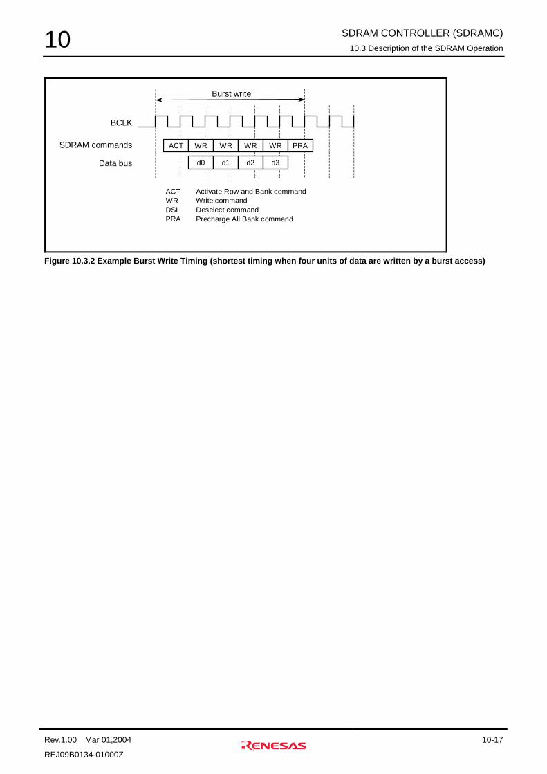
SDRAM CONTROLLER (SDRAMC) 10.3 Description of the SDRAM Operation
Rev.1.00 Mar 01,2004 10-17
REJ09B0134-01000Z
10
SDRAM commands ACT WR WR WR WR PRA
Data bus d0 d1 d2 d3
Burst write
ACT Activate Row and Bank command WR Write command DSL Deselect command PRA Precharge All Bank command
BCLK
Figure 10.3.2 Example Burst Write Timing (shortest timing when four units of data are written by a burst access)

SDRAM CONTROLLER (SDRAMC) 10.3 Description of the SDRAM Operation
Rev.1.00 Mar 01,2004 10-18
REJ09B0134-01000Z
10 (2) Example timing of single read and single write access
Figure 10.3.3 shows an example timing when data is read by a single access. Figure 10.3.4 shows an example timing when data is written normally. The access timing varies with the value set in the SDRAMi Timing Register. For details, refer to Section 10.4, “Access Timing Details.”
SDRAM commands ACT RD PRA DSL
D0–D31 d
Single read
ACT Activate Row and Bank command RD Read command DSL Deselect command PRA Precharge All Bank command
BCLK
Figure 10.3.3 Example Single Read Timing (when set for the shortest timing)
SDRAM commands ACT WR PRA
D0–D31 d
Single write
ACT Activate Row and Bank command WR Write command PRA Precharge All Bank command
BCLK
Figure 10.3.4 Example Single Write Timing (when set for the shortest timing)

SDRAM CONTROLLER (SDRAMC) 10.3 Description of the SDRAM Operation
Rev.1.00 Mar 01,2004 10-19
REJ09B0134-01000Z
10 10.3.3 Auto Refresh
An auto-refresh cycle is started by setting the DRFEN bit in SDRAM Refresh Control Register 1 (SDRF1) to 1. Thereafter, a refresh request is generated periodically by the refresh counter, invoking an auto-refresh cycle each time. However, because refresh requests are not accepted during a read/write access, an auto-refresh cycle may be kept waiting until the read/write access in progress finishes.
If the DRFEN bit in SDRAM Refresh Control Register 1 (SDRF1) is set to 1 during auto-refresh operation, a refresh request is generated immediately.
The refresh counter is halted during self-refresh. When an auto-refresh cycle starts after self-refresh is deactivated, the counter is reset and restarts counting.
Use SDRAM Refresh Control Register 1 (SDRF1) to set auto-refresh. Note that auto-refresh operation is performed on all SDRAM channels.
Figure 10.3.5 shows an example timing of the auto-refresh cycle.
SDRAM commands RFA DSL DSL
Auto-refresh cycle
DSL Deselect command RFA Auto Refresh command
BCLK
DREFW
Figure 10.3.5 Example Timing of the Auto-Refresh Cycle (where the DREFW bits are set to ‘0001’)

SDRAM CONTROLLER (SDRAMC) 10.3 Description of the SDRAM Operation
Rev.1.00 Mar 01,2004 10-20
REJ09B0134-01000Z
10 10.3.4 Self Refresh
SDRAM Refresh Control Register 0 (SDRF0) allows to control entering and exiting self-refresh mode. Control for entering and exiting self-refresh mode is exercised on all channels at the same time.
When self-refresh operation is enabled, self-refresh mode is entered into immediately after the auto-refresh cycle that was in progress. During self-refresh mode, the DCKE signal is held low (asserted). An auto-refresh cycle is started immediately after exiting self-refresh mode.
Figure 10.3.6 and Figure 10.3.7 show the example timing for entering and exiting self-refresh mode.
SDRAM commands RFA DSL DSL RFS
Auto-refresh cycle
DSL Deselect command RFA Auto Refresh command RFS Self Refresh Entry command
BCLK
DREFW
Self-refresh mode (CKE = low)
Figure 10.3.6 Example Timing when Entering Self-Refresh Mode (where the DREFW bits are set to ‘0001’)
SDRAM commands
DSL Deselect command RFA Auto Refresh command RFX Self Refresh Exit command
BCLK
Self-refresh off period
Self-refresh mode (CKE = low)
DSL RFA DSL DSL
Auto-refresh cycle
DREFW DREFW
RFX DSL
Figure 10.3.7 Example Timing when Exiting Self-Refresh Mode (where the DREFW bits are set to ‘0001’)

SDRAM CONTROLLER (SDRAMC) 10.3 Description of the SDRAM Operation
Rev.1.00 Mar 01,2004 10-21
REJ09B0134-01000Z
10 10.3.5 Initialization Sequencer
The SDRAMC has a sequencer that issues commands to initialize the SDRAM. The SDRAM initialization sequence should be invoked only once after reset. If the SDRAM initialization sequence is not performed at all or performed a number of times after reset, device operation cannot be guaranteed.
Note that the initialization sequence is performed on all channels at the same time. The initialization sequencer incorporated in the SDRAMC issues the Precharge All Bank command and then the
Auto Refresh command for ‘n’ times of refresh operations (n = 1–5). Use SDRAM Initialization Register 0 (SDIR0) to set the initialization sequencer timing, and SDRAM Initialization Register 1 (SDIR1) to start the initialization sequence.
An example timing of the initialization sequence is shown below. If DARFC is set to twice or more of auto-refresh operations, the initialization auto-refresh cycle is repeated a number of times as specified.
Figure 10.3.8 shows an example timing of the initialization sequence.
SDRAM commands
DSL Deselect command RFA Auto Refresh command PRA Precharge All Bank command
BCLK
Initialization precharge cycle
Initialization auto-refresh cycle
DPC DARFI
PRA DSL DSL DSL RFA DSL DSL DSL
The DINIST bit changes state to 0.
Figure 10.3.8 Example Timing of the Initialization Sequence
(where DPC bits = ‘001,’ DARFI bits = ‘0001’ and DARFC bits = ‘001’)

SDRAM CONTROLLER (SDRAMC) 10.3 Description of the SDRAM Operation
Rev.1.00 Mar 01,2004 10-22
REJ09B0134-01000Z
10 10.3.6 Mode Register Setup
Writing to the SDRAMi Mode Register (SDiMOD) allows to issue the Mode Register Set command to the SDRAM on each channel. The SDRAMi Mode Register (SDiMOD) should be set individually for each channel.
The following shows the timing in which the mode register setup operation is performed.
SDRAM commands
DSL Deselect command MRS Mode Register Set command
BCLK
Mode register setup cycle
MRS DSL DSL
3 cycles (fixed)
Figure 10.3.9 Timing of the Mode Register Setup Operation
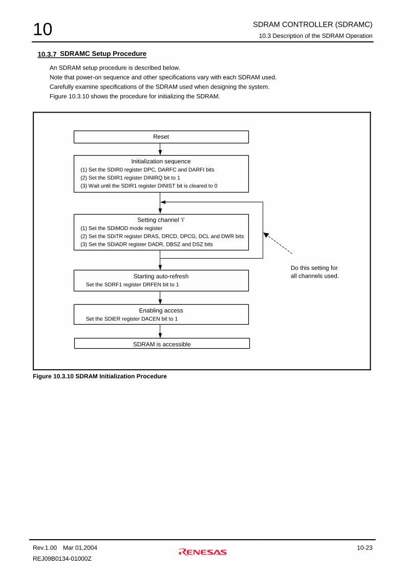
SDRAM CONTROLLER (SDRAMC) 10.3 Description of the SDRAM Operation
Rev.1.00 Mar 01,2004 10-23
REJ09B0134-01000Z
10 10.3.7 SDRAMC Setup Procedure
An SDRAM setup procedure is described below. Note that power-on sequence and other specifications vary with each SDRAM used. Carefully examine specifications of the SDRAM used when designing the system. Figure 10.3.10 shows the procedure for initializing the SDRAM.
Initialization sequence (1) Set the SDIR0 register DPC, DARFC and DARFI bits (2) Set the SDIR1 register DINIRQ bit to 1 (3) Wait until the SDIR1 register DINIST bit is cleared to 0
Reset
Setting channel ‘i’ (1) Set the SDiMOD mode register (2) Set the SDiTR register DRAS, DRCD, DPCG, DCL and DWR bits (3) Set the SDiADR register DADR, DBSZ and DSZ bits
Starting auto-refresh Set the SDRF1 register DRFEN bit to 1
Enabling access Set the SDiER register DACEN bit to 1
SDRAM is accessible
Do this setting for all channels used.
Figure 10.3.10 SDRAM Initialization Procedure

SDRAM CONTROLLER (SDRAMC) 10.3 Description of the SDRAM Operation
Rev.1.00 Mar 01,2004 10-24
REJ09B0134-01000Z
10 10.3.8 Procedure for Entering and Exiting Self-Refresh Mode
Figure 10.3.11 describes the procedure for entering and exiting self-refresh mode.
Entering self-refresh mode
Exiting self-refresh mode
Disabling access (1) Stop DMA access to SDRAM area if any in progress (2) In a program located in other than SDRAM area, disable access to
SDRAMC on all channels (DACENi = 0)
Staring self-refresh In a program located in other than SDRAM area, set DSFEN to 1
Self-refresh mode
Quitting self-refresh mode In a program located in other than SDRAM area, set DSFEN to 0
Enabling access In a program located in other than SDRAM area, enable access to SDRAMC (DACENi = 1)
Access enabled state (DRFEN = 1, DACENi = 1)
Access enabled state (DRFEN = 1, DACENi = 1)
Note: Before entering and exiting self-refresh mode, access to the SDRAM should be disabled. Therefore, self-refresh mode can neither be entered into nor exited from in a program or DMA operation that involves accessing the SDRAM. When writing a program, observe the following precautions.
Transfers on DMA channels accessing the SDRAM area if any in progress should be
disabled before entering self-refresh mode. The program to be executed when entering self-refresh mode, during self-refresh mode
or when exiting self-refresh mode should not include accessing operands in the SDRAM area or fetching (or prefetching) instructions from the SDRAM area.
Figure 10.3.11 Procedure for Entering and Exiting Self-Refresh Mode

SDRAM CONTROLLER (SDRAMC) 10.4 Access Timing Details
Rev.1.00 Mar 01,2004 10-25
REJ09B0134-01000Z
10 10.4 Access Timing Details
This section describes the relationship between read/write access timings and the values set in the SDRAMi Timing Register.
10.4.1 Single Read Timing
Figure 10.4.1 through Figure 10.4.3 show an example relationship between single read timings and the values set in the SDRAMi Timing Register.
Example single read timing 1 SDRAMi Timing Register 0 1 2 3 4 5 6 7 8 9 10 11 12 13 14 15 DRAS
0 0 0 0 0 0 0 0 0 0 0 0 0 0 1 0
16 17 18 19 20 21 22 23 24 25 26 27 28 29 30 31 DRCD DPCG DWR DCL
0 0 0 0 0 0 1 0 0 0 0 0 0 0 1 0
DRAS : 3BCLK
DRCD : 1BCLK
DPCG : 2BCLK
DWR : 1BCLK
DCL : 2BCLK
SDRAM commands ACT RD PRA DSL
D0–D31 d
BCLK
DSL
DRAS (ACT-PRA)
DRCD (ACT-RD)
Single read
DCL (RD-d)
DPCG (PRA-next)
ACT Activate Row and Bank command RD Read command DSL Deselect command PRA Precharge All Bank command
Figure 10.4.1 Example Single Read Timing 1
Example single read timing 2 SDRAMi Timing Register 0 1 2 3 4 5 6 7 8 9 10 11 12 13 14 15 DRAS
0 0 0 0 0 0 0 0 0 0 0 0 0 0 0 0
16 17 18 19 20 21 22 23 24 25 26 27 28 29 30 31 DRCD DPCG DWR DCL
0 0 0 1 0 0 1 0 0 0 0 0 0 0 1 0
DRAS : 1BCLK
DRCD : 2BCLK
DPCG : 2BCLK
DWR : 1BCLK
DCL : 2BCLK
SDRAM commands ACT RD PRA DSL
D0–D31 d
ACT Activate Row and Bank command RD Read command DSL Deselect command PRA Precharge All Bank command
BCLK
DRAS (ACT-PRA)
DRCD (ACT-RD)
Single read
DCL (RD-d)
DPCG (PRA-next)
DSL
If the period set by DRAS expires faster than RD, PRA is issued in the cycle next to RD.
Figure 10.4.2 Example Single Read Timing 2

SDRAM CONTROLLER (SDRAMC) 10.4 Access Timing Details
Rev.1.00 Mar 01,2004 10-26
REJ09B0134-01000Z
10
Example single read timing 3 SDRAMi Timing Register 0 1 2 3 4 5 6 7 8 9 10 11 12 13 14 15 DRAS
0 0 0 0 0 0 0 0 0 0 0 0 0 0 0 0
16 17 18 19 20 21 22 23 24 25 26 27 28 29 30 31 DRCD DPCG DWR DCL
0 0 0 1 0 0 1 0 0 0 0 0 0 0 1 1
DRAS : 1BCLK
DRCD : 2BCLK
DPCG : 2BCLK
DWR : 1BCLK
DCL : 3BCLK
ACT Activate Row and Bank command RD Read command DSL Deselect command PRA Precharge All Bank command
SDRAM commands ACT RD PRA DSL
D0–D31 d
BCLK
DRAS (ACT-PRA)
DRCD (ACT-RD)
Single read
DCL (RD-d)
DPCG (PRA-next)
DSL
If the period set by DRAS expires faster than RD, PRA is issued in the cycle next to RD.
DSL
Figure 10.4.3 Example Single Read Timing 3

SDRAM CONTROLLER (SDRAMC) 10.4 Access Timing Details
Rev.1.00 Mar 01,2004 10-27
REJ09B0134-01000Z
10 10.4.2 Single Write Timing
Figure 10.4.4 through Figure 10.4.6 show an example relationship between single write timings and the values set in the SDRAMi Timing Register.
Example single write timing 1 SDRAMi Timing Register 0 1 2 3 4 5 6 7 8 9 10 11 12 13 14 15 DRAS
0 0 0 0 0 0 0 0 0 0 0 0 0 0 1 0
16 17 18 19 20 21 22 23 24 25 26 27 28 29 30 31 DRCD DPCG DWR DCL
0 0 0 0 0 0 1 0 0 0 0 0 0 0 1 0
DRAS : 3BCLK
DRCD : 1BCLK
DPCG : 2BCLK
DWR : 1BCLK
DCL : 2BCLK
ACT Activate Row and Bank command WR Write command DSL Deselect command PRA Precharge All Bank command
SDRAM commands ACT WR PRA DSL
D0–D31 d
BCLK
DSL
DRAS (ACT-PRA)
DRCD (ACT-RD)
Single write
DWR (WR-PRA)
DPCG (PRA-next)
If the period set by DRAS exceeds expiration of the DWR period after WR command issuance, the DRAS period is applied.
Figure 10.4.4 Example Single Write Timing 1
Example single write timing 2 SDRAMi Timing Register 0 1 2 3 4 5 6 7 8 9 10 11 12 13 14 15 DRAS
0 0 0 0 0 0 0 0 0 0 0 0 0 0 0 0
16 17 18 19 20 21 22 23 24 25 26 27 28 29 30 31 DRCD DPCG DWR DCL
0 0 0 1 0 0 1 0 0 0 0 0 0 0 1 0
DRAS : 1BCLK
DRCD : 2BCLK
DPCG : 2BCLK
DWR : 1BCLK
DCL : 2BCLK
ACT Activate Row and Bank command WR Write command DSL Deselect command PRA Precharge All Bank command
If the period set by DRAS expires before expiration of the DWR period after WR command issuance,the DWR period is applied.
SDRAM commands ACT WR PRA DSL
D0–D31 d
BCLK
DRAS (ACT-PRA)
DRCD (ACT-RD)
Single write
DPCG (PRA-next)
DSL
DWR (WR-PRA)
Figure 10.4.5 Example Single Write Timing 2

SDRAM CONTROLLER (SDRAMC) 10.4 Access Timing Details
Rev.1.00 Mar 01,2004 10-28
REJ09B0134-01000Z
10
Example single write timing 3 SDRAMi Timing Register 0 1 2 3 4 5 6 7 8 9 10 11 12 13 14 15 DRAS
0 0 0 0 0 0 0 0 0 0 0 0 0 0 0 0
16 17 18 19 20 21 22 23 24 25 26 27 28 29 30 31 DRCD DPCG DWR DCL
0 0 0 1 0 0 1 1 0 0 0 0 0 0 1 0
DRAS : 1BCLK
DRCD : 2BCLK
DPCG : 2BCLK
DWR : 2BCLK
DCL : 2BCLK
ACT Activate Row and Bank command WR Write command DSL Deselect command PRA Precharge All Bank command
SDRAM commands
D0–D31
BCLK
ACT WR PRA DSL
d
DRAS (ACT-PRA)
DRCD (ACT-RD)
Single write
DPCG (PRA-next)
DSL
DWR (WR-PRA)
DSL
Figure 10.4.6 Example Single Write Timing 3

SDRAM CONTROLLER (SDRAMC) 10.4 Access Timing Details
Rev.1.00 Mar 01,2004 10-29
REJ09B0134-01000Z
10 10.4.3 Burst Read Timing
Figure 10.4.7 through Figure 10.4.9 show an example relationship between 4-data burst read timings and the values set in the SDRAMi Timing Register.
Example burst read timing 1 SDRAMi Timing Register 0 1 2 3 4 5 6 7 8 9 10 11 12 13 14 15 DRAS
0 0 0 0 0 0 0 0 0 0 0 0 0 0 1 0
16 17 18 19 20 21 22 23 24 25 26 27 28 29 30 31 DRCD DPCG DWR DCL
0 0 0 0 0 0 1 0 0 0 0 0 0 0 1 0
DRAS : 3BCLK
DRCD : 1BCLK
DPCG : 2BCLK
DWR : 1BCLK
DCL : 2BCLK
ACT Activate Row and Bank command RD Read command DSL Deselect command PRA Precharge All Bank command
SDRAM commands ACT RD
D0–D31 d0
BCLK
DRAS (ACT-PRA)
DRCD (ACT-RD)
Burst read
DCL (RD-d)
DPCG (PRA-next)
RD RD RD PRA DSL
d1 d2 d3
Figure 10.4.7 Example Burst Read Timing 1
Example burst read timing 2 SDRAMi Timing Register 0 1 2 3 4 5 6 7 8 9 10 11 12 13 14 15 DRAS
0 0 0 0 0 0 0 0 0 0 0 0 0 0 0 0
16 17 18 19 20 21 22 23 24 25 26 27 28 29 30 31 DRCD DPCG DWR DCL
0 0 0 1 0 0 1 0 0 0 0 0 0 0 1 0
DRAS : 1BCLK
DRCD : 2BCLK
DPCG : 2BCLK
DWR : 1BCLK
DCL : 2BCLK
ACT Activate Row and Bank command RD Read command DSL Deselect command PRA Precharge All Bank command
SDRAM commands ACT RD
D0–D31
BCLK
DRCD (ACT-RD)
Burst read
DCL (RD-d)
DPCG (PRA-next)
DSL RD RD RD
d0 d1 d2 d3
PRA DSL
DRAS (ACT-PRA)
Figure 10.4.8 Example Burst Read Timing 2

SDRAM CONTROLLER (SDRAMC) 10.4 Access Timing Details
Rev.1.00 Mar 01,2004 10-30
REJ09B0134-01000Z
10
Example burst read timing 3 SDRAMi Timing Register 0 1 2 3 4 5 6 7 8 9 10 11 12 13 14 15 DRAS
0 0 0 0 0 0 0 0 0 0 0 0 0 0 0 0
16 17 18 19 20 21 22 23 24 25 26 27 28 29 30 31 DRCD DPCG DWR DCL
0 0 0 1 0 0 1 0 0 0 0 0 0 0 1 1
DRAS : 1BCLK
DRCD : 2BCLK
DPCG : 2BCLK
DWR : 1BCLK
DCL : 3BCLK
ACT Activate Row and Bank command RD Read command DSL Deselect command PRA Precharge All Bank command
SDRAM commands ACT RD
D0–D31
BCLK
DRAS (ACT-PRA)
DRCD (ACT-RD)
Burst read
DCL (RD-d)
DPCG (PRA-next)
DSL RD RD RD
d0
PRA DSL DSL
d1 d2 d3
Figure 10.4.9 Example Burst Read Timing 3

SDRAM CONTROLLER (SDRAMC) 10.4 Access Timing Details
Rev.1.00 Mar 01,2004 10-31
REJ09B0134-01000Z
10 10.4.4 Burst Write Timing
Figure 10.4.10 through Figure 10.4.12 show an example relationship between 4-data burst write timings and the values set in the SDRAMi Timing Register.
Example burst write timing 1 SDRAMi Timing Register 0 1 2 3 4 5 6 7 8 9 10 11 12 13 14 15 DRAS
0 0 0 0 0 0 0 0 0 0 0 0 0 0 1 0
16 17 18 19 20 21 22 23 24 25 26 27 28 29 30 31 DRCD DPCG DWR DCL
0 0 0 0 0 0 1 0 0 0 0 0 0 0 1 0
DRAS : 3BCLK
DRCD : 1BCLK
DPCG : 2BCLK
DWR : 1BCLK
DCL : 2BCLK
ACT Activate Row and Bank command WR Write command DSL Deselect command PRA Precharge All Bank command
SDRAM commands ACT WR
D0–D31 d0
BCLK
DRAS (ACT-PRA)
DRCD (ACT-RD)
Burst write
DWR (WR-PRA)
DPCG (PRA-next)
WR WR WR
d1 d2 d3
PRA DSL
Figure 10.4.10 Example Burst Write Timing 1
Example burst write timing 2 SDRAMi Timing Register 0 1 2 3 4 5 6 7 8 9 10 11 12 13 14 15 DRAS
0 0 0 0 0 0 0 0 0 0 0 0 0 0 0 0
16 17 18 19 20 21 22 23 24 25 26 27 28 29 30 31 DRCD DPCG DWR DCL
0 0 0 1 0 0 1 0 0 0 0 0 0 0 1 0
DRAS : 1BCLK
DRCD : 2BCLK
DPCG : 2BCLK
DWR : 1BCLK
DCL : 2BCLK
ACT Activate Row and Bank command WR Write command DSL Deselect command PRA Precharge All Bank command
SDRAM commands ACT WR
D0–D31 d0
BCLK
DRAS (ACT-PRA)
DRCD (ACT-RD)
Burst write
DPCG (PRA-next)
DSL WR WR WR
d1 d2 d3
PRA DSL
DWR (WR-PRA)
Figure 10.4.11 Example Burst Write Timing 2

SDRAM CONTROLLER (SDRAMC) 10.4 Access Timing Details
Rev.1.00 Mar 01,2004 10-32
REJ09B0134-01000Z
10
Example burst write timing 3 SDRAMi Timing Register 0 1 2 3 4 5 6 7 8 9 10 11 12 13 14 15 DRAS
0 0 0 0 0 0 0 0 0 0 0 0 0 0 0 0
16 17 18 19 20 21 22 23 24 25 26 27 28 29 30 31 DRCD DPCG DWR DCL
0 0 0 1 0 0 1 1 0 0 0 0 0 0 1 0
DRAS : 1BCLK
DRCD : 2BCLK
DPCG : 2BCLK
DWR : 2BCLK
DCL : 2BCLK
ACT Activate Row and Bank command WR Write command DSL Deselect command PRA Precharge All Bank command
SDRAM commands ACT WR
D0–D31
BCLK
DRAS (ACT-PRA)
DRCD (ACT-RD)
Burst write
DPCG (PRA-next)
DSL WR WR WR
DWR (WR-PRA)
d0 d1 d2 d3
PRA DSLDSL
Figure 10.4.12 Example Burst Write Timing 3

SDRAM CONTROLLER (SDRAMC) 10.5 Example SDRAM Connections
Rev.1.00 Mar 01,2004 10-33
REJ09B0134-01000Z
10 10.5 Example SDRAM Connections
Figure 10.5.1 shows an example for connecting two pieces of a 64-Mbit SDRAM (x16) to the OPSP via a 32-bit bus. Similarly, Figure 10.5.2 shows an example for connecting two pieces of a 256-Mbit SDRAM (x16) to the OPSP via a 32-bit bus.
DCKE
OPSP
CKE RAS#DRAS#CAS#WE#
DQMUDQML
CLK CS#
BA1
A0–A11
DQ15 BCLKOUTDCS0#
DCAS#DWE#
DQM0DQM1
DQ14 DQ13 DQ12 DQ11 DQ10 DQ9 DQ8 DQ7 DQ6 DQ5 DQ4 DQ3 DQ2 DQ1 DQ0
64 Mbits × 16
A15/BA1A16/BA0
A29/MA0 – A18/MA11
BA0
12
D0 D1 D2 D3 D4 D5 D6 D7 D8 D9 D10 D11 D12 D13 D14 D15
CKE RAS#CAS#WE#
DQMUDQML
CLK CS#
BA1
A0–A11
DQ15 DQ14 DQ13 DQ12 DQ11 DQ10 DQ9 DQ8 DQ7 DQ6 DQ5 DQ4 DQ3 DQ2 DQ1 DQ0
BA0
D16 D17 D18 D19 D20 D21 D22 D23 D24 D25 D26 D27 D28 D29 D30 D31
DQM2DQM3
D0–D15
D16–D31
16
16
Figure 10.5.1 Example for Connecting Two Pcs. of 64-Mbit SDRAMs (x16)

SDRAM CONTROLLER (SDRAMC) 10.5 Example SDRAM Connections
Rev.1.00 Mar 01,2004 10-34
REJ09B0134-01000Z
10
DCKE
OPSP
CKE RAS#DRAS#CAS#WE#
DQMUDQML
CLK CS#
BA1
A0–A12
DQ15 BCLKOUTDCS0#
DCAS#DWE#
DQM0DQM1
DQ14 DQ13 DQ12 DQ11 DQ10 DQ9 DQ8 DQ7 DQ6 DQ5 DQ4 DQ3 DQ2 DQ1 DQ0
256 Mbits × 16
A15/BA1A16/BA0
A29/MA0 – A17/MA12
BA0
13
D0 D1 D2 D3 D4 D5 D6 D7 D8 D9 D10 D11 D12 D13 D14 D15
CKE RAS#CAS#WE#
DQMUDQML
CLK CS#
BA1
A0–A12
DQ15 DQ14 DQ13 DQ12 DQ11 DQ10 DQ9 DQ8 DQ7 DQ6 DQ5 DQ4 DQ3 DQ2 DQ1 DQ0
BA0
D16 D17 D18 D19 D20 D21 D22 D23 D24 D25 D26 D27 D28 D29 D30 D31
DQM2DQM3
D0–D15
D16–D31
16
16
Figure 10.5.2 Example for Connecting Two Pcs. of 256-Mbit SDRAMs (x16)

CHAPTER 11DMAC CHAPTER 11
DMAC

DMAC 11.1 Outline of the DMAC
Rev.1.00 Mar 01,2004 11-2
REJ09B0134-0100Z
11 11.1 Outline of the DMAC
The OPSP internally contains two-channel DMA Controllers (DMACs), allowing data to be transferred at high speed upon request from software, internal peripheral I/O or external pin or user IP module.
Following transfer patterns are available.
Data transfer between one external device and another Data transfer between an external device and an internal peripheral I/O or internal SRAM Data transfer between one internal peripheral I/O or internal SRAM and another Data transfer between a user IP module and an external device Data transfer between a user IP module and an internal peripheral I/O or internal SRAM Data transfer between one user IP module and another
Table 11.1.1 outlines the DMAC. Figure 11.1.1 shows a block diagram of the DMAC. The terms used in this chapter
are defined as follows: One-data transfer: A data transfer consisting of one read cycle and one write cycle performed by the DMAC. One-operand transfer: Consecutive data transfers performed by the DMAC on either channel. (In this case, the number of data transfers performed is set by a register.)
Burst transfer : A method of DMA transfer in which control of the bus is not released until a 1-operand transfer finishes.
Cycle steal transfer: A method of DMA transfer in which control of the bus is released for each 1-data transfer performed.
The letter ‘i’ in DMAi denotes 0–1.
Table 11.1.1 Outline of the DMAC
Item Outline
Number of channels 2 Transfer request Software, internal peripheral I/O, external pin (DREQ0, DREQ1
pins) or user IP module Maximum number of bytes transferred 64 Mbytes Address space 512 Mbytes Transfer data size Byte (8 bits), halfword (16 bits) or word (32 bits) Number of data transferred by one operand
1, 2, 4, 8, 16, 32, 64 or 128
Transfer mode Cycle steal mode or burst mode Channel priority DMA0 > DMA1
Priority fixed Interrupt request Generated when byte count = 0 Other Reload function (source, destination, byte count)
Two-dimensional addressing Fly-by transfer between SDRAM and user IP module possible Completion of 1-operand transfer or byte count = 0 selectable as end of DMA transfer

DMAC 11.1 Outline of the DMAC
Rev.1.00 Mar 01,2004 11-3
REJ09B0134-0100Z
11
Control Circuit
Internal Source (internal peripheral I/O)
Source Address
DMA0
Interrupt Signal
DACKi
Software Trigger Reload Register
Source Address Register
Destination address
Reload Register
Destination Address Register
Byte Count
Reload Register
Byte Count Register
Interrupt Signal Control Circuit
DMA1
External Source (external pin or user IP
module)
DM
A R
equest Selector
Figure 11.1.1 Block Diagram of the DMAC

DMAC 11.2 DMAC Related Registers
Rev.1.00 Mar 01,2004 11-4
REJ09B0134-0100Z
11 11.2 DMAC Related Registers
The following describes register mapping associated with the DMAC and each related register.
DMAC Register Mapping 1
Address b0
+0 address b7 b8
+1 addressb15 b16
+2 addressb23 b24
+3 address b31
H’00EF 8000 DMA Transfer Enable Register (DMAEN)
H’00EF 8004 DMA Interrupt Request Status Register (DMAISTS)
H’00EF 800C DMA Transfer End Detection Register (DMAEDET)
H’00EF 8010 DMA Arbitration Status Register (DMAASTS)
H’00EF 8014 DMA Fly-by Transfer Latency Control Register (DMAFBCR)
~ (Use of this area prohibited)
H’00EF 8100 DMA0 Control Register 0
(DMA0CR0)
H’00EF 8104 DMA0 Control Register 1 (DMA0CR1)
H’00EF 8108 DMA0 Current Source Address Register (DMA0CSA)
H’00EF 810C DMA0 Reload Source Address Register (DMA0RSA)
H’00EF 8110 DMA0 Current Destination Address Register (DMA0CDA)
H’00EF 8114 DMA0 Reload Destination Address Register (DMA0RDA)
H’00EF 8118 DMA0 Current Byte Count Register (DMA0CBCUT)
H’00EF 811C DMA0 Reload Byte Count Register (DMA0RBCUT)
H’00EF 8120 DMA0–2D Control Register (DMA02DCR)
~ (Use of this area prohibited)
H’00EF 8130 DMA0–2D Next Row Offset Register (DMA02DNROST)
H’00EF 8134 DMA0–2D Next Block Offset Register (DMA02DNBOST)
H’00EF 8138 DMA0–2D Next Line Offset Register (DMA02DNLOST)
~ (Use of this area prohibited)

DMAC 11.2 DMAC Related Registers
Rev.1.00 Mar 01,2004 11-5
REJ09B0134-0100Z
11 DMAC Register Mapping 2
Address b0
+0 address b7 b8
+1 addressb15 b16
+2 addressb23 b24
+3 addressb31
H’00EF 8200 DMA1 Control Register 0
(DMA1CR0)
H’00EF 8204 DMA1 Control Register 1 (DMA1CR1)
H’00EF 8208 DMA1 Current Source Address Register (DMA1CSA)
H’00EF 820C DMA1 Reload Source Address Register (DMA1RSA)
H’00EF 8210 DMA1 Current Destination Address Register (DMA1CDA)
H’00EF 8214 DMA1 Reload Destination Address Register (DMA1RDA)
H’00EF 8218 DMA1 Current Byte Count Register (DMA1CBCUT)
H’00EF 821C DMA1 Reload Byte Count Register (DMA1RBCUT)
H’00EF 8220 DMA1–2D Control Register (DMA12DCR)
~ (Use of this area prohibited)
H’00EF 8230 DMA1–2D Next Row Offset Register (DMA12DNROST)
H’00EF 8234 DMA1–2D Next Block Offset Register (DMA12DNBOST)
H’00EF 8238 DMA1–2D Next Line Offset Register (DMA12DNLOST)
~ (Use of this area prohibited)

DMAC 11.2 DMAC Related Registers
Rev.1.00 Mar 01,2004 11-6
REJ09B0134-0100Z
11 11.2.1 DMA Transfer Enable Register
DMA Transfer Enable Register (DMAEN) <Address: H’00EF 8000>
b0 1 2 3 4 5 6 7 8 9 10 11 12 13 14 b15
0 0 0 0 0 0 0 0 0 0 0 0 0 0 0 0
b16 17 18 19 20 21 22 23 24 25 26 27 28 29 30 b31
DMSK0 DMSK1 DEN0 DEN1 0 0 0 0 0 0 0 0 0 0 0 0 0 0 0 0
* This register can be accessed bytewise (in 8 bits), halfwordwise (in 16 bits) or wordwise (in 32 bits)
<After reset: H’0000 0000>
b Bit Name Function R W
0–15 No functions assigned. Fix these bits to 0. 0 0 16 DMSK0
DEN0 write mask bit 0 : Write to DEN0 masked 1 : Write to DEN0 unmasked
0 Note
17 DMSK1 DMA1 transfer enable bit
0 : Write to DEN1 masked 1 : Write to DEN1 unmasked
0 Note
18–23 No functions assigned. Fix these bits to 0. 0 0 24 DEN0
DMA0 transfer enable bit 0 : Disable DMA transfer on DMA0 1 : Enable DMA transfer on DMA0
R W
25 DEN1 DMA1 transfer enable bit
0 : Disable DMA transfer on DMA1 1 : Enable DMA transfer on DMA1
R W
26–31 No functions assigned. Fix these bits to 0. 0 0 Note: This means that writing data “0” has no effect, and that data “1” written to the bit is not retained.

DMAC 11.2 DMAC Related Registers
Rev.1.00 Mar 01,2004 11-7
REJ09B0134-0100Z
11 (1) DMSKi (DENi write mask) bits (b16–b17)
These bits control masking of write to the DMAi transfer enable bit (DENi). If when the DMAi transfer enable bit is accessed for write, the corresponding DMSKi bit is found cleared to 0,
no data is written to the DMAi transfer enable bit. If when the DMAi transfer enable bit is accessed for write, the corresponding DMSKi bit is found set to 1,
write to the DMAi transfer enable bit is enabled and its value can be altered. The value “1” written to this bit is not retained. Therefore, make sure this bit is set to 1 each time the DMAC
writes to the DMAi transfer enable bit.
(2) DENi (DMAi transfer enable) bits (b24–25)
These bits disable or enable DMA transfer. Clearing this bit to 0 disables DMA transfer on DMAi. Setting this bit to 1 enables DMA transfer on DMAi. Even when this bit is cleared to 0, the DMA request bit (DREQ) in the DMAi Control Register changes state
upon DMA request input to the DMAC. This bit is automatically cleared to 0 if DMA transfer end condition is detected when the DMA transfer enable
clear bit (ECLR) in DMAi Control Register 1 = 1.
Temporary halt of DMA transfer If all of the DMAi transfer enable bits are cleared Note 1 during a 1-operand transfer in cycle steal mode, the
1-operand transfer being executed is temporarily halted. However, control of the bus is not released to other channels during a 1-operand transferNote 2. Thereafter, the 1-operand transfer is resumed by setting the DMAi transfer enable bits back to 1. To abort the temporarily halted 1-operand transfer without resuming it, set the DMA transfer status clear bit (DSCLR) in DMAi Control Register 1 to 1.
Note 1: To halt a 1-operand transfer being executed in cycle steal mode, all of the DMAi transfer enable bits
should be cleared. If the DMAi transfer enable bit for the other channel than the channel in which the transfer is to be temporarily halted remains set, device operation thereafter cannot be guaranteed.
Note 2: In no event will control of the bus be released to other channels during a 1-operand transfer, regardless of whether the transfer is being executed in cycle steal mode or in burst mode. To execute a 1-operand transfer on another channel, therefore, abort the temporarily halted 1-operand transfer on the current channel.

DMAC 11.2 DMAC Related Registers
Rev.1.00 Mar 01,2004 11-8
REJ09B0134-0100Z
11 11.2.2 DMA Interrupt Request Status Register
DMA Interrupt Request Status Register (DMAISTS) <Address: H’00EF 8004>
b0 1 2 3 4 5 6 7 8 9 10 11 12 13 14 b15
0 0 0 0 0 0 0 0 0 0 0 0 0 0 0 0
b16 17 18 19 20 21 22 23 24 25 26 27 28 29 30 b31
DISTS0 DISTS1 0 0 0 0 0 0 0 0 0 0 0 0 0 0 0 0 * This register can be accessed bytewise (in 8 bits), halfwordwise (in 16 bits) or wordwise (in 32 bits)
<After reset: H’0000 0000>
b Bit Name Function R W
0–15 No functions assigned. Fix these bits to 0. 0 N 16 DISTS0
DMA0 interrupt request status bit 0 : DMA0 interrupt not requested 1 : DMA0 interrupt requested
0 N
17 DISTS1 DMA1 interrupt request status bit
0 : DMA1 interrupt not requested 1 : DMA1 interrupt requested
0 N
18–31 No functions assigned. Fix these bits to 0. 0 N
Note: This is a read-only register.
(1) DISTSi (DMAi interrupt request status) bits (b16–b17)
These bits allow to inspect the DMAi interrupt request status. If this bit is set to 1, it means that a DMAi interrupt request has been generated to the Interrupt Controller.
Set (= 1) conditions
If DMA transfer end condition is detected when DMA transfer end interrupt requests are enabled (DMA transfer end interrupt request enable bit (DIRQ) in DMAi Control Register 0 = 1), the DMAi transfer end detection bit (DEDETi) in the DMA Transfer End Detection Register is set to 1. At this time, this bit also is set to 1.
Clear (= 0) conditions
This bit is cleared to 0 under the following conditions: • When the DMAi transfer end detection bit in the DMA Transfer End Detection Register for the channel
in which an interrupt request was generated is cleared. • When the DMA transfer end interrupt request enable bit for the channel in which an interrupt request
was generated is cleared.

DMAC 11.2 DMAC Related Registers
Rev.1.00 Mar 01,2004 11-9
REJ09B0134-0100Z
11 11.2.3 DMA Transfer End Detection Register
DMA Transfer End Detection Register (DMAEDET) <Address: H’00EF 8008>
b0 1 2 3 4 5 6 7 8 9 10 11 12 13 14 b15
0 0 0 0 0 0 0 0 0 0 0 0 0 0 0 0
b16 17 18 19 20 21 22 23 24 25 26 27 28 29 30 b31
DEDET0 DEDET1 0 0 0 0 0 0 0 0 0 0 0 0 0 0 0 0
* This register can be accessed bytewise (in 8 bits), halfwordwise (in 16 bits) or wordwise (in 32 bits)
<After reset: H’0000 0000>
b Bit Name Function R W
0–15 No functions assigned. Fix these bits to 0. 0 0 16 DEDET0
DMA0 transfer end condition detect bit 0 : DMA0 transfer end condition not detected 1 : DMA0 transfer end condition detected
R Note
17 DEDET1 DMA1 transfer end condition detect bit
0 : DMA1 transfer end condition not detected 1 : DMA1 transfer end condition detected
R Note
18–31 No functions assigned. Fix these bits to 0. 0 0 Note: This means that writing data “0” has no effect, and that data “1” written to the bit is not retained.
(1) DEDETi (DMAi transfer end condition detect) bits (b16-b17)
These bits allow to inspect the status of whether DMA transfer end condition on DMAi has been detected. Once this bit is set to 1, it remains set unless it is explicitly cleared by writing 0 in software as described below.
Set (= 1) conditions This bit is set to 1 when DMA transfer finishes.
Clear (= 0) conditions This bit is cleared by writing 0 in software. At this time, write 0 to all bits in the register that do not need to be cleared. Writing 0 to any bit in software
has no effect, and the bit retains the value it had before the write.

DMAC 11.2 DMAC Related Registers
Rev.1.00 Mar 01,2004 11-10
REJ09B0134-0100Z
11 11.2.4 DMA Arbitration Status Register
DMA Arbitration Status Register (DMAASTS) <Address: H’00EF 800C>
b0 1 2 3 4 5 6 7 8 9 10 11 12 13 14 b15
0 0 0 0 0 0 0 0 0 0 0 0 0 0 0 0
b16 17 18 19 20 21 22 23 24 25 26 27 28 29 30 b31
DASTS0 DASTS1 0 0 0 0 0 0 0 0 0 0 0 0 0 0 0 0
* This register can be accessed bytewise (in 8 bits), halfwordwise (in 16 bits) or wordwise (in 32 bits)
<After reset: H’0000 0000>
b Bit Name Function R W
0–15 No functions assigned. Fix these bits to 0. 0 N 16 DASTS0
DMA0 arbitration status bit
0 : No 1-operand transfer in progress on DMA0 1 : 1-operand transfer in progress on DMA0
R N
17 DASTS1 DMA1 arbitration status bit
0 : No 1-operand transfer in progress on DMA1 1 : 1-operand transfer in progress on DMA1
R N
26–31 No functions assigned. Fix these bits to 0. 0 N Note: This is a read-only register.
(1) DASTSi (DMAi arbitration status) bits (b16, b17)
These bits allow to inspect the status of whether a 1-operand transfer on channel 'i' is being executed.
Set (= 1) conditions
This bit is set to 1 when a 1-operand transfer on the channel has started.
Clear (= 0) conditions
This bit is cleared to 0 under the following conditions: When the 1-operand transfer has finished normally. When the DMA transfer has been aborted by the DMA transfer status clear bit (DSCLR) in DMAi Control Register 1.

DMAC 11.2 DMAC Related Registers
Rev.1.00 Mar 01,2004 11-11
REJ09B0134-0100Z
11 11.2.5 DMA Fly-by Transfer Latency Control Register
DMA Fly-by Transfer Latency Control Register (DMAFBCR) <Address: H’00EF 8010>
b0 1 2 3 4 5 6 7 8 9 10 11 12 13 14 b15
0 0 0 0 0 0 0 0 0 0 0 0 0 0 0 0
b16 17 18 19 20 21 22 23 24 25 26 27 28 29 30 b31
FBRL FBWL 0 0 0 0 0 0 0 0 0 0 0 0 0 0 0 0
* This register can be accessed bytewise (in 8 bits), halfwordwise (in 16 bits) or wordwise (in 32 bits)
<After reset: H’0000 0000>
b Bit Name Function R W
0–19 No functions assigned. Fix these bits to 0. 0 0 20–23 FBRL
DMA fly-by transfer read latency
0000 : 0BCLK 0001 : 1BCLK 1110 : 14BCLK 1111 : 15BCLK
R W
24–27 No functions assigned. Fix these bits to 0. 0 0 28–31 FBWL
DMA fly-by transfer write latency
0000 : 0BCLK 0001 : 1BCLK 1110 : 14BCLK 1111 : 15BCLK
R W
This register is used to set the SDRAM access latency when performing a fly-by transfer. Refer to the value set in
the target SDRAMC when setting this register.
(1) FBRL (fly-by transfer read latency)
These bits set the number of wait cycles to be inserted from when SDRAM access starts to when a read strobe is output. The fly-by transfer read latency is calculated based on the value that was set in the RAS-CAS latency setting bits (DRCD) of the SDRAMi Timing Register.
The equation to calculate the fly-by transfer read latency is shown below.
Fly-by transfer read latency calculation formula Fly-by transfer read latency = DRCD bits – 1
For example, if the RAS-CAS latency is set to 2 BCLKs (DRCD bits = '01'), then the fly-by transfer read
latency is 0 BCLK. Therefore, set the value ‘0000’ in these bits. Note: For fly-by transfers to be performed normally, DCRD should be set to 2 BCLKs or more.

DMAC 11.2 DMAC Related Registers
Rev.1.00 Mar 01,2004 11-12
REJ09B0134-0100Z
11 (2) FBWL (fly-by transfer write latency)
These bits set the number of wait cycles to be inserted from when SDRAM access starts to when a write strobe is output.
The fly-by transfer write latency is calculated based on the value that was set in the RAS-CAS latency setting bits (DRCD) and CAS latency setting bits (DCL) of the SDRAMi Timing Register. The equation to calculate the fly-by transfer write latency is shown below.
Fly-by transfer write latency calculation formula Fly-by transfer write latency = DRCD bits + DCL bits + 2
For example, if the RAS-CAS latency and the CAS latency are set to 2 BCLKs (DRCD bits = '01') and 2
BCLKs (DCL bits = '010'), respectively, then the fly-by transfer write latency is 5 BCLKs. Therefore, set the value '0101' in the FBWL bits.

DMAC 11.2 DMAC Related Registers
Rev.1.00 Mar 01,2004 11-13
REJ09B0134-0100Z
11 11.2.6 DMAi Control Register 0
DMA0 Control Register 0 (DMA0CR0) <Address: H’00EF 8100>
DMA1 Control Register 0 (DMA1CR0) <Address: H’00EF 8200>
b0 1 2 3 4 5 6 7 8 9 10 11 12 13 14 b15
DREQ SZSEL MDSEL DIRQ DSEL OPSEL ALSEL BRLOD SRLOD DRLOD0 0 0 0 0 0 0 0 0 0 0 0 0 0 0 0
b16 17 18 19 20 21 22 23 24 25 26 27 28 29 30 b31
SAMOD DAMOD FB TDIR DSE REQSEL 0 0 0 0 0 0 0 0 0 0 0 0 0 0 0 0
* This register can be accessed bytewise (in 8 bits), halfwordwise (in 16 bits) or wordwise (in 32 bits)
<After reset: H’0000 0000>
b Bit Name Function R W0 DREQ
DMA request bit 0 : DMA not requested 1 : DMA requested
R W
1 No functions assigned. Fix this bit to 0. 0 02,3 SZSEL
Transfer data size select bits 00 : Byte (8 bits) 01 : Halfword (16 bits) 10 : Word (32 bits) 11 : Settings prohibited
R W
4 No functions assigned. Fix this bit to 0. 0 05 MDSEL
DMA transfer mode select bit 0 : Burst mode 1 : Cycle steal mode
R W
6 No functions assigned. Fix this bit to 0. 0 07 DIRQ
DMA transfer end interrupt request enable bit 0 : Disable interrupt 1 : Enable interrupt
R W
8 DSEL DMA transfer condition select bit
0 : Transfer until 1-operand transfer finishes 1 : Transfer until byte count reaches 0
R W
9–11 OPSEL One-operand transfer data quantity select bits
000 : 1 data 001 : 2 data 010 : 4 data 011 : 8 data 100 : 16 data 101 : 32 data 110 : 64 data 111 : 128 data
R W
12 ALSEL DACK signal output active level select bit
0 : DACK is output as active-high 1 : DACK is output as active-low
R W
13 BRLOD DMA byte count reload function enable bit
0 : Disable byte count reload function 1 : Enable byte count reload function
R W
14 SRLOD DMA source address reload function enable bit
0 : Disable source address reload function 1 : Enable source address reload function
R W
15 DRLOD DMA destination address reload function enable bit
0 : 0: Disable destination address reload function 1 : Enable destination address reload function
R W
16,17 SAMOD DMA source addressing mode select bits
00 : Fixed 01 : Plus direction 10 : Two-dimensional addressing 11 : Minus direction
R W
18,19 DAMOD DMA destination addressing mode select bits
00 : Fixed 01 : Plus direction 10 : Two-dimensional addressing 11 : Minus direction
R W

DMAC 11.2 DMAC Related Registers
Rev.1.00 Mar 01,2004 11-14
REJ09B0134-0100Z
11 20 FB
Fly-by transfer control bit 0 : Disable fly-by transfer (dual-address transfer) 1 : Enable fly-by transfer
R W
21–23 TDIR DMA transfer direction select bits
When FB = 0 Source Destination 000 : Internal resource → internal resource 001 : Internal resource → external device 010 : External device → internal resource 011 : External device → external device 100 – 111: Settings prohibited
When FB = 1 Source Destination 000–010: Settings prohibited 011 : User IP module → SDRAM 100 ~ 110: Settings prohibited 111 : SDRAM → User IP module
R W
24,25 DSE DMA request input sense mode select bits
00 : Rising edge sensitive 01 : High level sensitive 10 : Falling edge sensitive 11 : Low level sensitive
R W
26 No functions assigned. Fix this bit to 0. 0 027–31 REQSEL
DMA request source select bits 00000 : Software trigger 00001 : DREQ0 (external pin input or user IP module)00010 : DREQ1 (external pin input or user IP module)00011–00111 : Settings prohibited 01000 : SIO0 receive 01001 : SIO0 transmit 01010 : SIO1 receive 01011 : SIO1 transmit 01100–01111 : Settings prohibited 10000 : MFT0 10001 : MFT1 10010 : MFT2 10011 : MFT3 10100 : MFT4 10101 : MFT5 10110–11111 : Settings prohibited
R W
Note 1: If software trigger is selected for the DMA request source, the DMA request bit can be set to 1 at any time no matter how the DMA transfer enable bit is set or irrespective of the 1-operand transfer status. However, when clearing the DMA request bit or altering the set values of the other bits in DMAi Control Register 0, check to see that the transfer being executed on the channel is not a 1-operand transfer (DMA Arbitration Status Register DASTSi bit = 0) and DMA transfer is disabled (DMA Transfer Enable Register DENi bit = 0). If the values of DMAi Control Register 0 are altered under any other condition, device operation cannot be guaranteed.
Note 2: If other than software trigger is selected for the DMA request source, the set values of the DMA request and other bits in DMAi Control Register 0 can only be altered when no 1-operand transfer on the channel is in progress and DMA transfer is disabled. If the values of DMAi Control Register 0 are altered under any other condition, device operation cannot be guaranteed.
Note 3: Except software trigger, do not select the same DMA request source for both channels. Note 4: When software trigger is selected, make sure the DMA request input sense mode select bits are set to “edge sensitive.”

DMAC 11.2 DMAC Related Registers
Rev.1.00 Mar 01,2004 11-15
REJ09B0134-0100Z
11 (1) DREQ (DMA request) bit (b0)
This bit allows to inspect whether a DMA request has been generated from any source. Also, when software trigger is selected with the DMA request source select bits in DMAi Control Register 0
(REQSEL= ‘00000’), this bit is used to set or clear a DMA request. This bit changes state depending on DMA request input to the DMAC irrespective of how the DMA Transfer
Enable Register is set, and the condition under which it is set or cleared varies depending on how the DMA request source select bits and DMA request input sense mode select bits (DSE) in DMAi Control Register 0 are set, as described below.
<When software trigger is selected>
When software trigger is selected, make sure the DMA request source select bits are set to “edge sensitive” (DSE = ‘00’ or ‘10’). Level sensitive mode cannot be selected.
Set (= 1) conditions
This bit is set to 1 by writing 1 in software. This causes a DMA request to occur. Clear (= 0) conditions
This bit is cleared to 0 under following conditions: When the bit is explicitly cleared by writing 0 in software.
When a 1-operand transfer has started corresponding to this bit.
<When external input or internal source is selected, both level sensitive>
Set (= 1) conditions This bit is set to 1 when the active level selected with the DMA request input sense mode select bits and
the level of DMA request input match (i.e., DMA request asserted). Clear (= 0) conditions
This bit is cleared to 0 when the active level selected with the DMA request input sense mode select bits and the level of DMA request input dot not match (i.e., DMA request dropped).
(If a DMA request is dropped before being accepted, it is not held on and the DMA request bit is cleared. Therefore, if input mode is chosen to be level sensitive, the DMA request should be held active until it is accepted.
Note: If the selected DMA request source is other than software trigger, do not set the DMA request bit by
writing 1 in software. Otherwise, device operation cannot be guaranteed. <When external input or internal source is selected, both edge sensitive>
Set (= 1) conditions
This bit is set to 1 when a DMA request is generated on the internal peripheral I/O side or the active edge selected with the DMA request input sense mode select bits is detected on the input to the DMAC (i.e., DMA request asserted).
Once set to 1, the DMA request bit remains set until it is cleared under a given condition irrespective of whether DMA request input is turned on or off thereafter.
Clear (= 0) conditions
This bit is cleared to 0 under the following conditions: When the bit is explicitly cleared by writing 0 in software. When a 1-operand transfer has started corresponding to this bit.
Note 1: If the selected DMA request source is other than software trigger, do not set the DMA request bit by
writing 1 in software. Otherwise, device operation cannot be guaranteed. Note 2: If the DMA request source select bits (REQSEL[0:4]) in DMAi Control Register 0 have been set, the
DMA request bit for the relevant channel should always be cleared to 0 before enabling DMA transfer.

DMAC 11.2 DMAC Related Registers
Rev.1.00 Mar 01,2004 11-16
REJ09B0134-0100Z
11 (2) SZSEL (transfer data size select) bits (b2–b3)
These bits select the size in bits of 1-data transfer. Also, the increment/decrement values of the following registers vary depending on the data size selected
with these bits. (The DMAi Current Byte Counter only decrements.)
DMAi Current Source Address Register DMAi Current Destination Address Register DMAi Current Byte Counter
The increment/decrement values change as follows: Byte (8 bits): 1 Halfword (16 bits): 2 Word (32 bits): 4
(3) MDSEL (DMA transfer mode select) bit (b5)
This bit selects DMA transfer mode. Figure 11.2.1 shows an example operation in each transfer mode. When this bit is cleared to 0, transfer mode changes to burst mode, in which the DMAC retains control of the
bus until a 1-operand transfer finishes. To perform a fly-by transfer, set this bit to 0. When this bit is set to 1, transfer mode changes to cycle steal mode, in which the DMAC relinquishes control
of the bus for each 1-data transfer performed.

DMAC 11.2 DMAC Related Registers
Rev.1.00 Mar 01,2004 11-17
REJ09B0134-0100Z
11 <Example operation in burst mode> When transfer data size = byte (8 bits) and 1-operand transfer data quantity = 2 data
Status of bus control
DMAC
CPU
Read Write
Cleared in software
DMA request bit
DMA current byte count
DMA transfer end condition detect bit
H'0000 0003 H'0000 0002 H'0000 0001 H'0000 0000
During bus control continuously retained mode, control of the bus is not released until the 1-operand transfer finishes.: DMA request accepted
Transfer of one data
1-operand transfer 1-operand transfer
<Example operation in cycle steal mode> When transfer data size = halfword (16 bits) and 1-operand transfer data quantity = 2
Status of bus control
DMAC
CPU
Read Write
DMA request bit
DMA current byte count
DMA transfer end condition detect bit
H'0000 0003 H'0000 0002 H'0000 0001 H'0000 0000
During cycle steal mode, control of the bus is released to the CPU for each 1-data transfer performed.During a 1-operand transfer, however, DMA requests for other channels are not accepted. : DMA request accepted
1-operand transfer 1-operand transfer
Read Write Read Write Read Write
Read Write Read Write Read Write
Transfer of one data Transfer of one data Transfer of one data
Transfer of one data Transfer of one data Transfer of one data Transfer of one data
Figure 11.2.1 Example Operation in Each DMA Transfer Mode

DMAC 11.2 DMAC Related Registers
Rev.1.00 Mar 01,2004 11-18
REJ09B0134-0100Z
11 (4) DIRQ (DMA transfer end interrupt request enable) bit (b7)
This bit selects whether or not to generate a DMA transfer end interrupt request to the ICU (Interrupt Controller).
If this bit is cleared to 0, the corresponding bit (DISTSi) in the DMA Interrupt Status Register is not set to 1 even when DMA transfer end condition is detected, nor is an interrupt request to the ICU generated.
If this bit is set to 1, the corresponding bit (DISTSi) in the DMA Interrupt Status Register is set to 1 when DMA transfer end condition is detected, and an interrupt request to the ICU is generated.
Interrupt requests to the ICU are generated independently for each channel. (5) DSEL (DMA transfer condition select) bit (b8)
This bit selects DMA transfer condition. If this bit is cleared to 0, data transfer is performed until the 1-operand transfer started by one DMA request
finishes. If this bit is set to 1, data transfer is performed until the byte count started by one DMA request reaches 0. Figure 11.2.2 shows an example transfer for each DMA transfer condition selected.
When DSEL = 0
Read Write Read Write Read Write Read Write
1-operand transfer 1-operand transfer
When DSEL = 1
DMAC status Read Write Read Write
DMA request bit
Read Write Read Write
1-operand transfer 1-operand transfer
Read Write Read Write
1-operand transfer
Channel arbitration
Internal signal Internal signal
Until the byte count reaches 0
Omitted
DMAC status
DMA request bit
Figure 11.2.2 Example Operation for Each DMA Transfer Condition Selected by DSEL
(6) OPSEL (1-operand transfer data quantity select) bits (b9–b11)
These bits select the data quantity transferred by a 1-operand transfer. If the DMA transfer condition select bit (DSEL) = 0, as many data as set by these bits are transferred for one DMA request received. If DSEL = 1, as many data as set by these bits are transferred repeatedly until the byte count reaches 0. In this case, DMA requests are arbitrated between channels at intervals from one transfer to another.
No matter how DSEL is set, DMA requests for other channels are not accepted until all quantities of data set by these bits have been transferred (by 1-operand transfer).
Note: If the transfer data size select bits are set to “byte (8 bits)” (SZSEL = ‘00’), make sure the values set in the DMA Current Byte Counter and DMA Reload Byte Counter are integer multiples of the number of transfer data selected with the 1-operand transfer data quantity select bits. If the transfer data size select bits are set to “halfword (16 bits)” or “word (32 bits)” (SZSEL = ‘01’ or ‘10’), make sure the values set in the DMA Current Byte Counter and DMA Reload Byte Counter are even multiples of or multiples of 4 times the number of transfer data selected with the 1-operand transfer data quantity select bits, respectively.

DMAC 11.2 DMAC Related Registers
Rev.1.00 Mar 01,2004 11-19
REJ09B0134-0100Z
11 (7) ALSEL (DACK signal output active level select) bit (b12)
This bit selects the active level of the DMA acknowledge signal that indicates that a DMA request has been
accepted.
If this bit is cleared to 0, the DACK pin outputs a high-level signal as DMA acknowledge for the DMA request
source accepted.
If this bit is set to 1, the DACK pin outputs a low-level signal as DMA acknowledge for the DMA request source
accepted.
The DMAACK active level for user IP modules should be chosen to be “high” (ALSEL bit = 0).
Note 1: If other than external pins are selected for the DMA request source, do not set this bit to 1. Otherwise,
device operation cannot be guaranteed.
(8) BRLOD (DMA byte count reload function enable) bit (b13) This bit selects whether or not reload the byte counter when DMA transfer end condition (DMAi Current Byte
Count Register value = H’0000 0000) is detected. If this bit is cleared to 0, the byte counter is not reloaded. If this bit is set to 1, the content of the DMAi Reload Byte Count Register is reloaded into the DMAi Current
Byte Count Register when the DMA transfer end condition is detected.
(9) SRLOD (DMA source address reload function enable) bit (b14)
This bit selects whether or not reload the source address when DMA transfer end condition (DMAi Current Byte Count Register value = H’0000 0000) is detected.
If this bit is cleared to 0, the source address is not reloaded. If this bit is set to 1, the content of the DMAi Reload Source Address Register is reloaded into the DMAi
Current Source Address Register when the DMA transfer end condition is detected.
(10) DRLOD (DMA destination address reload function enable) bit (b15) This bit selects whether or not reload the destination address when DMA transfer end condition (DMAi
Current Byte Count Register value = H’0000 0000) is detected. If this bit is cleared to 0, the destination address is not reloaded. If this bit is set to 1, the content of the DMAi Reload Destination Address Register is reloaded into the DMAi
Current Destination Address Register when the DMA transfer end condition is detected. (11) SAMOD (DMA source addressing mode select) bits (b16–b17)
These bits select the direction in which the DMAi Current Source Address Register is changed (fixed, plus or minus direction or 2-dimensional addressing).
If 2-dimensional addressing is selected with these bits, the DAMOD (DMA destination addressing mode select) bits cannot be set to “2-dimensional addressing.”
If DMA transfer in the direction from user IP module to SDRAM is selected (TDIR bits = ‘011’) during fly-by transfer mode (FB bit = 1), this bit has no effect.

DMAC 11.2 DMAC Related Registers
Rev.1.00 Mar 01,2004 11-20
REJ09B0134-0100Z
11 (12) DAMOD (DMA destination addressing mode select) bits (b18–b19)
These bits select the direction in which the DMAi Current Destination Address Register is changed (fixed, plus or minus direction or 2-dimensional addressing).
If 2-dimensional addressing is selected with these bits, the SAMOD (DMA source addressing mode select) bits cannot be set to “2-dimensional addressing.”
If DMA transfer in the direction from SDRAM to user IP module is selected (TDIR bits = ‘111’) during fly-by transfer mode (FB bit = 1), this bit has no effect.
Table 11.2.1 shows the increment/decrement values of the DMAi Current Source Address Register and DMAi Current Destination Address Register.
Table 11.2.1 Increment/Decrement Values of the DMAi Current Source Address Register and DMAi Current
Destination Address Register
Addressing mode (SAMOD or DAMOD) Transfer data size select bits SZSEL[0:1] in DMAi Control
Register 0 "00"
(Fixed) "01"
(Plus direction) "11"
(Minus direction) "10"
(2-dimensional)
“00” (8 bits) ±0 +1 -1 Settings prohibited“01” (16 bits) ±0 +2 -2 Settings prohibited“10” (32 bits) ±0 +4 -4 2-dimensional
(13) FB (DMA fly-by transfer select) bit (b20)
This bit selects whether or not to use a fly-by transfer for the DMA transfer between the SDRAM and user IP module.
If this bit is cleared to 0, the DMA transfer is performed by a dual-address transfer. If this bit is set to 1, the DMA transfer is performed by a fly-by transfer. A fly-by transfer is supported for only the transfer between the SDRAM and user IP module. To perform a
fly-by transfer, set the transfer data size select bits (SZSEL) to 32 bits and the SDRAM bus width select bit (BSZ) to 32 bits, then select burst mode for the DMA transfer mode.
Figure 11.2.3 shows an example fly-by transfer.
Fly-by transfer from the SDRAM to a user IP module
ACT DSL RD RD RD RD
BCLKDMA request bit
SDRAM commands
D0–D31
FBMODE
FBRS
FBWS
Figure 11.2.3 Example Fly-By Transfer
Note: When performing a fly-by transfer, always be sure to set the source or destination address on the user
IP module side (addresses in BSEL1 space).

DMAC 11.2 DMAC Related Registers
Rev.1.00 Mar 01,2004 11-21
REJ09B0134-0100Z
11 (14) TDIR (DMA transfer direction select) bits (b21–b23)
These bits select the direction of DMA transfer. If the direction of DMA transfer is erroneously set, device operation cannot be guaranteed.
(15) DSE (DMA request input sense mode select) bits (b24–b25)
If the DMA request source select bits (REQSEL) are set to “software trigger” or “external pin input,” use these bits to select input sense mode for the DMA request signal that is presented to the DMAC.
Note: If internal peripheral I/O is selected for the DMA request source, these bits do not need to be set.
(16) REQSEL (DMA request source select) bits (b27–b31)
These bits select the DMA request source. If software trigger is selected with these bits (REQSEL[0:4] = ‘00000’), use the DMA request bit (DREQ) in
DMAi Control Register 0 to set or clear a DMA request. The DMA request source select bits can only be accessed for write when DMA transfer is disabled (DMA
Transfer Enable Register DENi bit = 0). Also, if any value has been written to the DMA request source select bits, always be sure to enable DMA transfer after clearing the DMA request bit in DMAi Control Register 0.
Furthermore, since a fly-by transfer is invoked by a DMA request from the user IP module, software trigger or internal peripheral I/O cannot be selected for REQSEL.

DMAC 11.2 DMAC Related Registers
Rev.1.00 Mar 01,2004 11-22
REJ09B0134-0100Z
11 11.2.7 DMAi Control Register 1
DMA0 Control Register 1 (DMA0CR1) <Address: H’00EF 8104>
DMA1 Control Register 1 (DMA1CR1) <Address: H'00EF 8204>
b0 1 2 3 4 5 6 7 8 9 10 11 12 13 14 b15
ECLR DSCLR0 0 0 0 0 0 0 0 0 0 0 0 0 0 0 0
b16 17 18 19 20 21 22 23 24 25 26 27 28 29 30 b31
0 0 0 0 0 0 0 0 0 0 0 0 0 0 0 0
* This register can be accessed bytewise (in 8 bits), halfwordwise (in 16 bits) or wordwise (in 32 bits)
<After reset: H’0000 0000>
b Bit Name Function R W
0–6 No functions assigned. Fix these bits to 0. 0 0 7 ECLR
DMA transfer enable clear bit 0 : Do not clear DMAi transfer enable bit upon
detection of DMA transfer end
1 : Clear DMAi transfer enable bit upon detection of DMA transfer end
R W
8–14 No functions assigned. Fix these bits to 0. 0 0 15 DSCLR
DMA transfer status clear bit 0 : No operation 1 : Clear DMA transfer status to abort the DMA
transfer in progress
R *
16–31 No functions assigned. Fix these bits to 0. 0 0 Note: The asterisk (*) in the W column denotes that writing 0 has no effect, and that data “1” written to the bit is not
retained.
(1) ECLR (DMA transfer enable clear) bit (b7)
This bit selects whether or not to clear the DMAi transfer enable bit for the corresponding channel in the DMA Transfer Enable Register when DMA transfer end condition (DMAi Current Byte Count Register value = H’0000 0000) is detected.
If this bit is cleared to 0, the DMAi transfer enable bit is not cleared to 0 even when the DMA transfer end condition is detected.
If this bit is set to 1, the DMAi transfer enable bit is cleared to 0 when the DMA transfer end condition is detected.
Note: If the DMA transfer enable clear bit for a channel is accessed for write while a 1-operand transfer in that
channel is under way, device operation cannot be guaranteed
(2) DSCLR (DMA transfer status clear) bit (b15)
If a 1-operand transfer is temporarily halted in the middle of operation, use this bit to abort the rest of the 1-operand transfer.
Note: DMA transfer on all channels must be disabled before this bit can be set. If this bit is set otherwise,
device operation cannot be guaranteed.

DMAC 11.2 DMAC Related Registers
Rev.1.00 Mar 01,2004 11-23
REJ09B0134-0100Z
11 11.2.8 DMAi Current Source Address Register
DMA0 Current Source Address Register (DMA0CSA) <Address: H’00EF 8108>
DMA1 Current Source Address Register (DMA1CSA) <Address: H'00EF 8208>
b0 1 2 3 4 5 6 7 8 9 10 11 12 13 14 b15
DCSA 0 0 0 ? ? ? ? ? ? ? ? ? ? ? ? ?
b16 17 18 19 20 21 22 23 24 25 26 27 28 29 30 b31
? ? ? ? ? ? ? ? ? ? ? ? ? ? ? ?
* This register can be accessed bytewise (in 8 bits), halfwordwise (in 16 bits) or wordwise (in 32 bits)
<After reset: Indeterminate>
b Bit Name Function R W
0–2 No functions assigned. Fix these bits to 0. 0 0 3–31 DCSA
DMAi current source address bits DMAi current source address A3–A31 R W
The DMAi Current Source Address Register is used to set the start address at the source of DMA transfer. The value in this register may change for each 1-data transfer performed. For details about the
increment/decrement value, refer to the description of the transfer data size select bits (SZSEL) and DMA source addressing mode select bits (SAMOD) in Section 11.2.6, “DMAi Control Register 0.”
The DMAi Current Source Address Register must always be set regardless of whether the reload function is enabled or not.
Note 1: This register should be set in such a way that DMA transfer is performed within the address boundary
aligned to the selected transfer data size. (If the transfer data size is chosen to be 16 bits or 32 bits, the halfword aligned address (even address) or the word aligned address (multiple of 4) should be set in the DMAi Current Source Address Register, respectively.)
Note 2: The DMAi Current Source Address Register can only be accessed for write when no 1-operand transfer on
the channel is in progress (DMA Arbitration Status Register DASTSi bit = 0) and DMA transfer is disabled (DMA Transfer Enable Register DENi bit = 0). If any value is written to the DMAi Current Source Address Register under any other condition, device operation cannot be guaranteed.

DMAC 11.2 DMAC Related Registers
Rev.1.00 Mar 01,2004 11-24
REJ09B0134-0100Z
11 11.2.9 DMAi Reload Source Address Register
DMA0 Reload Source Address Register (DMA0RSA) <Address: H’00EF 810C>
DMA1 Reload Source Address Register (DMA1RSA) <Address: H'00EF 820C>
b0 1 2 3 4 5 6 7 8 9 10 11 12 13 14 b15
DRSA 0 0 0 ? ? ? ? ? ? ? ? ? ? ? ? ?
b16 17 18 19 20 21 22 23 24 25 26 27 28 29 30 b31
? ? ? ? ? ? ? ? ? ? ? ? ? ? ? ?
* This register can be accessed bytewise (in 8 bits), halfwordwise (in 16 bits) or wordwise (in 32 bits)
<After reset: Indeterminate>
b Bit Name Function R W
0–2 No functions assigned. Fix these bits to 0. 0 0 3–31 DRSA
DMAi reload source address bits DMAi reload source address A3–A31 R W
The DMAi Reload Source Address Register is used to set the address to be reloaded into the DMAi Current
Source Address Register. To enable the reload function, set the DMA source address reload function enable bit (SRLOD) in DMAi Control Register 0 to 1. In this case, values must be set in both the DMAi Current Source Address Register and DMAi Reload Source Address Register.
Note: This register should be set in such a way that DMA transfer is performed within the address boundary aligned
to the selected transfer data size.

DMAC 11.2 DMAC Related Registers
Rev.1.00 Mar 01,2004 11-25
REJ09B0134-0100Z
11 11.2.10 DMAi Current Destination Address Register
DMA0 Current Destination Address Register (DMA0CDA) <Address: H’00EF 8110>
DMA1 Current Destination Address Register (DMA1CDA) <Address: H'00EF 8210>
b0 1 2 3 4 5 6 7 8 9 10 11 12 13 14 b15
DCDA 0 0 0 ? ? ? ? ? ? ? ? ? ? ? ? ?
b16 17 18 19 20 21 22 23 24 25 26 27 28 29 30 b31
? ? ? ? ? ? ? ? ? ? ? ? ? ? ? ?
* This register can be accessed bytewise (in 8 bits), halfwordwise (in 16 bits) or wordwise (in 32 bits)
<After reset: Indeterminate>
b Bit Name Function R W
0–2 No functions assigned. Fix these bits to 0. 0 0 3–31 DCDA
DMAi current destination address bits DMAi current destination address A3–A31 R W
The DMAi Current Destination Address Register is used to set the start address at the destination of DMA
transfer. The value in this register may change for each 1-data transfer performed. For details about the
increment/decrement value, refer to the description of the transfer data size select bits (SZSEL) and DMA destination addressing mode select bits (DAMOD) in Section 11.2.6, “DMAi Control Register 0.”
The DMAi Current Destination Address Register must always be set regardless of whether the reload function is enabled or not.
Note 1: This register should be set in such a way that DMA transfer is performed within the address boundary
aligned to the selected transfer data size. (If the transfer data size is chosen to be 16 bits or 32 bits, the halfword aligned address (even address) or the word aligned address (multiple of 4) should be set in the DMAi Current Destination Address Register, respectively.)
Note 2: The DMAi Current Destination Address Register can only be accessed for write when no 1-operand
transfer on the channel is in progress (DMA Arbitration Status Register DASTSi bit = 0) and DMA transfer is disabled (DMA Transfer Enable Register DENi bit = 0). If any value is written to the DMAi Current Destination Address Register under any other condition, device operation cannot be guaranteed.

DMAC 11.2 DMAC Related Registers
Rev.1.00 Mar 01,2004 11-26
REJ09B0134-0100Z
11 11.2.11 DMAi Reload Destination Address Register
DMA0 Reload Destination Address Register (DMA0RDA) <Address: H’00EF 8114>
DMA1 Reload Destination Address Register (DMA1RDA) <Address: H'00EF 8214>
b0 1 2 3 4 5 6 7 8 9 10 11 12 13 14 b15
DRDA 0 0 0 ? ? ? ? ? ? ? ? ? ? ? ? ?
b16 17 18 19 20 21 22 23 24 25 26 27 28 29 30 b31
? ? ? ? ? ? ? ? ? ? ? ? ? ? ? ?
* This register can be accessed bytewise (in 8 bits), halfwordwise (in 16 bits) or wordwise (in 32 bits)
<After reset: Indeterminate>
b Bit Name Function R W
0–2 No functions assigned. Fix these bits to 0. 0 0 3–31 DRDA
DMAi reload destination address bits DMAi reload destination address A3–A31 R W
The DMAi Reload Destination Address Register is used to set the address to be reloaded into the DMAi Current
Destination Address Register. To enable the reload function, set the DMA destination address reload function enable bit (DRLOD) in DMAi Control Register 0 to 1. In this case, values must be set in both the DMAi Current Destination Address Register and DMAi Reload Destination Address Register.
Note: This register should be set in such a way that DMA transfer is performed within the address boundary aligned
to the selected transfer data size. (If the transfer data size is chosen to be 16 bits or 32 bits, the halfword aligned address (even address) or the word aligned address (multiple of 4) should be set in the DMAi Reload Destination Address Register, respectively.)

DMAC 11.2 DMAC Related Registers
Rev.1.00 Mar 01,2004 11-27
REJ09B0134-0100Z
11 11.2.12 DMAi Current Byte Count Register
DMA0 Current Byte Count Register (DMA0CBCUT) <Address: H’00EF 8118>
DMA1 Current Byte Count Register (DMA1CBCUT) <Address: H'00EF 8218>
b0 1 2 3 4 5 6 7 8 9 10 11 12 13 14 b15
DCBCUT 0 0 0 0 0 0 ? ? ? ? ? ? ? ? ? ?
b16 17 18 19 20 21 22 23 24 25 26 27 28 29 30 b31
? ? ? ? ? ? ? ? ? ? ? ? ? ? ? ?
* This register can be accessed bytewise (in 8 bits), halfwordwise (in 16 bits) or wordwise (in 32 bits)
<After reset: Indeterminate>
b Bit Name Function R W
0–5 No functions assigned. Fix these bits to 0. 0 0 6–31 DCBCUT
DMAi current byte count bits DMAi current byte count R W
The DMAi Current Byte Count Register is used to set the number of bytes to be DMA transferred. The DMA current byte count set in this register is decremented for each 1-data transfer performed, and when the
count reaches 0, DMA transfer finishes (termination by byte count = 0). At this time, the corresponding bit in the DMA Transfer End Condition Detect Register is set to 1. The amount by which the DMA current byte count is decremented each time is given below.
–1 when the transfer data size = 8 bits (DMAi Control Register 0 SZSEL bits = ‘00’) –2 when the transfer data size = 16 bits (DMAi Control Register 0 SZSEL bits = ‘01’) –4 when the transfer data size = 32 bits (DMAi Control Register 0 SZSEL bits = ‘10’)
The number of bytes that can be transferred is one byte when the set value of the DMAi Current Byte Count Register is H'000 0001, 64M - 1 bytes when the set value is H'3FFF FFFF, or 64 Mbytes (maximum transferable bytes) when the set value is H'000 0000.
The DMAi Current Byte Count Register must always be set regardless of whether the reload function is enabled or not.
Note 1: The DMAi Current Byte Count Register should be set in such a way that the byte count reaches 0 when the
last data in a 1-operand transfer has been transferred.
When the transfer data size = 8 bits, integer multiple of the number of data in a 1-operand transfer (e.g., x1, x2, x3 and so on) When the transfer data size = 16 bits, even multiple of the number of data in a 1-operand transfer (e.g.,
x2, x4, x6 and so on) When the transfer data size = 32 bits, multiple of 4 times the number of data in a 1-operand transfer (e.g.,
x4, x8, x12 and so on)
If any other value than those given above is set, device operation cannot be guaranteed. Note 2: The DMAi Current Byte Count Register can only be accessed for write when no 1-operand transfer on the
channel is in progress (DMA Arbitration Status Register DASTSi bit = 0) and DMA transfer is disabled (DMA Transfer Enable Register DENi bit = 0). If any value is written to the DMAi Current Byte Count Register under any other condition, device operation cannot be guaranteed.

DMAC 11.2 DMAC Related Registers
Rev.1.00 Mar 01,2004 11-28
REJ09B0134-0100Z
11 11.2.13 DMAi Reload Byte Count Register
DMA0 Reload Byte Count Register (DMA0RBCUT) <Address: H’00EF 811C>
DMA1 Reload Byte Count Register (DMA1RBCUT) <Address: H’00EF 821C>
b0 1 2 3 4 5 6 7 8 9 10 11 12 13 14 b15
DRBCUT 0 0 0 0 0 0 ? ? ? ? ? ? ? ? ? ?
b16 17 18 19 20 21 22 23 24 25 26 27 28 29 30 b31
? ? ? ? ? ? ? ? ? ? ? ? ? ? ? ?
* This register can be accessed bytewise (in 8 bits), halfwordwise (in 16 bits) or wordwise (in 32 bits)
<After reset: Indeterminate>
b Bit Name Function R W
0–5 No functions assigned. Fix these bits to 0. 0 0 6–31 DRBCUT
DMAi reload byte count bits DMAi reload byte count R W
The DMAi Reload Byte Count Register is used to set the byte count to be reloaded into the DMAi Current Byte
Count Register. To enable the reload function, set the DMA byte count reload function enable bit (BRLOD) in DMAi Control Register 0 to 1. In this case, values must be set in both the DMAi Current Byte Count Register and DMAi Reload Byte Count Register.
Note: The DMAi Reload Byte Count Register should be set in such a way that the byte count reaches 0 when the
last data in a 1-operand transfer has been transferred.
When the transfer data size = 8 bits, integer multiple of the number of data in a 1-operand transfer (e.g., x1, x2, x3 and so on)
When the transfer data size = 16 bits, even multiple of the number of data in a 1-operand transfer (e.g., x2, x4, x6 and so on)
When the transfer data size = 32 bits, multiple of 4 times the number of data in a 1-operand transfer (e.g., x4, x8, x12 and so on)
If any other value than those given above is set, device operation cannot be guaranteed.

DMAC 11.2 DMAC Related Registers
Rev.1.00 Mar 01,2004 11-29
REJ09B0134-0100Z
11 11.2.14 DMAi 2-Dimensional Addressing Control Register
DMA0 2-Dimensional Addressing Control Register (DMA02DCR) <Address: H’00EF 8120>
DMA1 2-Dimensional Addressing Control Register (DMA12DCR) <Address: H’00EF 8220>
b0 1 2 3 4 5 6 7 8 9 10 11 12 13 14 b15
DCWN DRN 0 0 0 0 0 0 0 0 0 0 0 0 0 0 0 0
b16 17 18 19 20 21 22 23 24 25 26 27 28 29 30 b31
DBN 0 0 0 0 0 0 0 0 0 0 0 0 0 0 0 0
* This register can be accessed bytewise (in 8 bits), halfwordwise (in 16 bits) or wordwise (in 32 bits)
<After reset: H’0000 0000>
b Bit Name Function R W0–7 DCWN
DMAi block per-row words 0000 0000 : 1 word
0000 0001 : 2 words
1111 1111 : 256 words
R W
8–15 DRN DMAi block lines
0000 0000 : 1 line
0000 0001 : 2 lines
1111 1111 : 256 lines
R W
16–21 No functions assigned. Fix these bits to 0. 0 0 22–31 DBN
DMAi blocks 00 0000 0000 : 1 block
00 0000 0001 : 2 blocks
11 1111 1111 : 1,024 blocks
R W
(1) DCWN (DMA block per-row words) bits (b0–b7)
These bits set the number of words per row in one block.
Note: Make sure the number of words per row set in these bits is the same as or an integer multiple of the number of data that was set by the 1-operand transfer data quantity select bits (OPSEL). If any other value than that is set, device operation cannot be guaranteed.
(2) DRN (DMA block lines) bits (b8–b15)
These bits set the number of lines in one block.
(3) DBN (DMA blocks) bits (b22–b31)
These bits set the number of blocks in one line.

DMAC 11.2 DMAC Related Registers
Rev.1.00 Mar 01,2004 11-30
REJ09B0134-0100Z
11
Start address Number of words per
block row (DCWN)
Block 0 Block n
Number of next row offset
words (DNROST)
Number of blocks in one line
(DBN)
Block m
~
Number of next line offset words
(DNLOST)
Start address
+
number of transfer bytes
: 1 word (32 bits)
Number of next block offset
words (DNBOST)
Number of block lines
(DRN)
Block n + 1
Figure 11.2.4 Conceptual Diagram of 2-Dimensional Addressing

DMAC 11.2 DMAC Related Registers
Rev.1.00 Mar 01,2004 11-31
REJ09B0134-0100Z
11 11.2.15 DMAi 2-Dimensional Next Row Offset Register
DMA0 2-Dimensional Next Row Offset Register (DMA02DNROST) <Address: H’00EF 8130>
DMA1 2-Dimensional Next Row Offset Register (DMA12DNROST) <Address: H’00EF 8230>
b0 1 2 3 4 5 6 7 8 9 10 11 12 13 14 b15
DNROST ? ? ? ? ? ? ? ? ? ? ? ? ? ? ? ?
b16 17 18 19 20 21 22 23 24 25 26 27 28 29 30 b31
? ? ? ? ? ? ? ? ? ? ? ? ? ? 0 0
* This register can be accessed bytewise (in 8 bits), halfwordwise (in 16 bits) or wordwise (in 32 bits).
<After reset: Indeterminate>
b Bit Name Function R W0–29 DNROST
DMAi 2-dimensional next row offset words setting bits
Number of DMAi 2-dimensional next row offset words R W
30,31 No functions assigned. Fix these bits to 0. 0 0
(1) DNROST (DMAi 2-dimensional next row offset words) bits
These bits set the number of words to be added to the current source or current destination address in order to calculate the start address of the next row in a block when DMA transfer for one row of data in one block has finished during 2-dimensional addressing.

DMAC 11.2 DMAC Related Registers
Rev.1.00 Mar 01,2004 11-32
REJ09B0134-0100Z
11 11.2.16 DMAi 2-Dimensional Next Block Offset Register
DMA0 2-Dimensional Next Block Offset Register (DMA02DNBOST) <Address: H’00EF 8134>
DMA1 2-Dimensional Next Block Offset Register (DMA12DNBOST) <Address: H’00EF 8234>
b0 1 2 3 4 5 6 7 8 9 10 11 12 13 14 b15
DNBOST ? ? ? ? ? ? ? ? ? ? ? ? ? ? ? ?
b16 17 18 19 20 21 22 23 24 25 26 27 28 29 30 b31
? ? ? ? ? ? ? ? ? ? ? ? ? ? 0 0
* This register can be accessed bytewise (in 8 bits), halfwordwise (in 16 bits) or wordwise (in 32 bits).
<After reset: Indeterminate>
b Bit Name Function R W0–29 DNBOST
DMAi 2-dimensional next block offset words setting bits
Number of DMAi 2-dimensional next block offset words
R W
30,31 No functions assigned. Fix these bits to 0. 0 0
(1) DNBOST (DMAi 2-dimensional next block offset words) bits
These bits are used to calculate the start address of the next block when DMA transfer for one block of data has finished during 2-dimensional addressing.

DMAC 11.2 DMAC Related Registers
Rev.1.00 Mar 01,2004 11-33
REJ09B0134-0100Z
11 11.2.17 DMAi 2-Dimensional Next Line Offset Register
DMA0 2-Dimensional Next Line Offset Register (DMA02DNLOST) <Address: H’00EF 8138>
DMA1 2-Dimensional Next Line Offset Register (DMA12DNLOST) <Address: H’00EF 8238>
b0 1 2 3 4 5 6 7 8 9 10 11 12 13 14 b15
DNLOST ? ? ? ? ? ? ? ? ? ? ? ? ? ? ? ?
b16 17 18 19 20 21 22 23 24 25 26 27 28 29 30 b31
? ? ? ? ? ? ? ? ? ? ? ? ? ? 0 0
* This register can be accessed bytewise (in 8 bits), halfwordwise (in 16 bits) or wordwise (in 32 bits).
<After reset: Indeterminate>
b Bit Name Function R W0–29 DNLOST
DMAi 2-dimensional next line offset words setting bits
Number of DMAi 2-dimensional next line offset words R W
30,31 No functions assigned. Fix these bits to 0. 0 0
(1) DNLOST (DMAi 2-dimensional next line offset words) bits
These bits set the number of words to be added to the current source or current destination address in order to calculate the start address of the next block line when DMA transfer for one line of block data has finished during 2-dimensional addressing.

DMAC 11.3 Description of the DMAC Functions
Rev.1.00 Mar 01,2004 11-34
REJ09B0134-0100Z
11 11.3 Description of the DMAC Functions
The following describes each function of the DMAC.
11.3.1 Channel Arbitration by the DMAC
The DMAC arbitrates DMA requests between channels. If no DMA requests are generated from any channel during this arbitration process, control of the bus is transferred to the CPU. If DMA requests are generated from either channel, the DMAC outputs a signal to request control of the bus. DMA requests are arbitrated every cycle until the request for control of the bus is accepted. When control of the bus is granted, the DMAC starts a 1-operand transfer for the channel it determined by arbitration in the preceding cycles. The channel is held on until the 1-operand transfer thus started finishes.
Channel priority is given below.
DMA0 > DMA1
11.3.2 About Selection of DMA Request Input Sense Modes
From a total of 13 sources of DMA requests (12 for the internal peripheral I/O and external devices and one for software), the DMAC selects the source of a particular DMA request on each channel (DMA0, DMA1) individually. The DMA request input sense mode select bits (DSE) should be set only when software trigger or external source has been selected for the DMA request source. If any other DMA request source is selected, writing to these bits has no effect and the bits therefore do not need to be set.
The following describes level and edge-sensitive request inputs.
(1) Example processing for level-sensitive requests accepted
When level sense mode is selected (DSE = ‘01’ or ‘10’), presence of DMA requests is determined by the DMA request input level. Since DMA requests are not retained internally in the DMAC, the DMA request input level should be held on until it is confirmed that the DMA request has been accepted.
Figure11.3.1 shows example processing for level-sensitive requests accepted.
BCLK
DMAC status
DMA request input
(chosen to be “high level sensitive”)
DMA acknowledge output
(chosen to be “active-high”)
DMA request bit
The DMA request should be held on until DMA acknowledge output for that request is asserted.
: DMA request sampling points
Read Write
1-operand transfer starts
Figure11.3.1 Example Processing for Level-Sensitive Requests Accepted
When level sense mode is selected, to allow a time in which DMA request input can be dropped, DMA
requests on the current channel are not accepted for 2 system clock cycles after the 1-operand transfer has finished.
Figure 11.3.2 shows an example timing diagram.

DMAC 11.3 Description of the DMAC Functions
Rev.1.00 Mar 01,2004 11-35
REJ09B0134-0100Z
11
BCLK
DMAC status
DMA request input
(chosen to be “high level sensitive”)
DMA acknowledge output
(chosen to be “active-high”)
DMA request bit
: DMA request sampling points
Read Write
1-operand transfer
(DMA request bit mask period) To ensure that the next channel arbitration will not be affected for reasons that the 1-operand transfer period is short and the DMA request bit cannot be cleared in time after DMA request is dropped, the DMA request bit is ignored during this period.
Channel arbitration starts
Figure 11.3.2 DMA Request Mask Period during Level Sense Mode
Therefore, even when DMA request level is held on after DMA request has been accepted on a channel
which has had level sense mode selected (i.e., DMA request is kept active), the DMAC relinquishes control of the bus during the DMA request mask period because no DMA requests are sampled active during that time.
The following shows operation of the DMAC when DMA request level is held on even after DMA request has been accepted on a channel which has had level sense mode selected.
The DMAC temporarily relinquishes control of the bus, and when the DMAC regains control of the bus thereafter, it arbitrates DMA requests between channels and accepts one that has the highest priority. Figure 11.3.3 shows an example operation in that case.
DMAC
CPU
DMA request input
(chosen to be “high level sensitive”)
DMA request bit
Status of bus
control
Control of the bus is temporarily returned to the CPU. Then, after control of the bus is
regained, two DMA requests are accepted.
: DMA requests accepted
1-operand transfer 1-operand transfer
Figure 11.3.3 Example Operation when DMA Request Level is Still Retained after Being Accepted

DMAC 11.3 Description of the DMAC Functions
Rev.1.00 Mar 01,2004 11-36
REJ09B0134-0100Z
11 (2) Example processing for edge-sensitive requests accepted
The rising or falling edge of the DMA request input (whichever active) is recognized as a DMA request. Upon detection of the active edge, the DMA request bit (DREQ) in DMAi Control Register 0 is set to 1. Thereafter, even when the DMA request input level changes, the DMA request bit remains set. When the DMA request is accepted and a DMA acknowledge signal is asserted, the DMA request bit is automatically cleared to 0. (The DMA acknowledge signals output to the internal peripheral I/O or internal user IP module cannot be referenced from the outside.)
Read Write Read
1-operand transfer starts
The DMA request bit is set upon detection of the
active edge.
Even when the DMA request input level changes,
the DMA request bit remains set.
When the DMA request is accepted, a DMA acknowledge
signal is asserted and the DMA request bit is cleared.
: DMA request sampling points
If the DMA request input is detected active
while the DMA request bit has been cleared,
the DMA request bit is set again.
(Once recognized, DMA request is retained.)
BCLK
DMAC status
DMA request input
(chosen to be “falling edge sensitive”)
DMA acknowledge output
(chosen to be “active-low”)
DMA request bit
Figure 11.3.4 Example Processing for Edge-Sensitive Requests Accepted
Since edge-sensitive DMA requests are retained by keeping the DMA request bit intact as described above,
new active edges occurring on DMA request input while the DMA request bit remains set are ignored. Figure 11.3.4 shows example processing for edge-sensitive requests accepted.

DMAC 11.3 Description of the DMAC Functions
Rev.1.00 Mar 01,2004 11-37
REJ09B0134-0100Z
11 11.3.3 Page Access to External Devices
The following settings enable page access to external devices.
(1) Burst mode is selected
(2) Internal resource to or from external device transfer is selected for the DMA transfer direction
(3) The 1-operand transfer data quantity select bits are set to other than “one data” (OPSEL = ‘000’)
(4) Page access is enabled by BSEL Control Register 1
Note: Page access cannot be performed when external device to external device transfer is selected for the DMA transfer direction.
Figure 11.3.5 shows an example access to external devices.
When page access is disabled
Read Read Read Read Write Write Write Write
1-operand transfer
BCLK
BSEL
RS
D0–D31
DMAC
When page access is enabled
Read ReadWrite
1-operand transfer
BCLK
BSEL
RS
D0–D31
DMACReadWrite ReadWrite Write Read ReadWrite
1-operand transfer
Write
Figure 11.3.5 Example Access to External Devices

DMAC 11.3 Description of the DMAC Functions
Rev.1.00 Mar 01,2004 11-38
REJ09B0134-0100Z
11 11.3.4 DMA Transfer Cycles
(1) Transfer method
The DMAC supports two methods of DMA transfer: dual-address transfer and fly-by transfer (single-address transfer). However, a fly-by transfer can only be performed for data transfer between external SDRAM and user IP module.
(2) Transfer cycles
The following shows types of DMA transfer cycles.
(1) Arbitration cycle This is the cycle from when the DMA request bit is set to 1 to when a DMA transfer read cycle starts.
(2) DMA transfer read cycle This is the transfer data read cycle. The number of BCLKs in this cycle varies with the wait cycles required for the target to be accessed.
(3) DMA transfer write cycle This is the transfer data write cycle. The number of BCLKs in this cycle varies with the wait cycles required for the target to be accessed.
(4) DMA transfer idle cycle A DMA transfer idle cycle of one BCLK in duration is inserted during DMA transfer between one external device and another, as well as during an interval between DMA transfer read cycle and DMA transfer write cycle and an interval between DMA transfer write cycle and DMA transfer read cycle. However, no idle cycles are inserted after the last write cycle in a 1-operand transfer.
Figure 11.3.6 shows an example DMA transfer in burst mode and cycle steal mode.

DMAC 11.3 Description of the DMAC Functions
Rev.1.00 Mar 01,2004 11-39
REJ09B0134-0100Z
11
Burst mode
BCLK
DMAC
CPU
DMA request bit
Status of
bus control
1-data transfer 1-data transfer 1-data transfer 1-data transfer
Read Write Read Write Read Write WriteRead
1-operand transfer
(2)(1) (2) (3) (2) (3) (3) (3)(2) (4)
Cycle steal mode
BCLK
DMAC
CPU
DMA request bit
Status of
bus control
1-data transfer 1-data transfer
Read Write WriteRead
1-operand transfer
(1) (2) (3) (4) (4) (3)(2) (4)
Shown here is example timing under the following conditions: DMA request input sense mode is set to “edge sensitive” Transfer between one internal I/O and another is selected
(1): Transition to hold and arbitration cycle (2): DMA transfer read cycle (3): DMA transfer write cycle (4): Return and arbitration cycle
Figure 11.3.6 Example DMA Transfer between One Internal Peripheral I/O and Another

DMAC 11.3 Description of the DMAC Functions
Rev.1.00 Mar 01,2004 11-40
REJ09B0134-0100Z
11 11.3.5 DMA Transfer End Conditions
DMA transfer end condition is detected when the value of the DMAi Current Byte Count Register has been decremented to H’0000 0000 (all data transfers completed). Note: Make sure the following values are set in the DMAi Current Byte Count Register and DMAi Reload Byte
Count Register. If any other value than that is set, device operation cannot be guaranteed.
When the transfer data size = 8 bits, integer multiple of the number of data in a 1-operand transfer (e.g., x1, x2 and so on)
When the transfer data size = 16 bits, even multiple of the number of data in a 1-operand transfer (e.g., x2, x4 and so on)
When the transfer data size = 32 bits, multiple of 4 times the number of data in a 1-operand transfer (e.g., x4, x8 and so on)
The following shows operations that are performed pursuant to detection of the DMA transfer end condition.
Generation of an interrupt request:
The DEDETi bit for the corresponding channel in the DMA Transfer End Detection Register is set to 1. If the DMA transfer end interrupt request enable bit (DIRQ) in DMAi Control Register 0 = 1, a DMA transfer end interrupt request (internal signal) is generated to the ICU (Interrupt Controller).
Clearing of the DMAi transfer enable bit:
If the DMA transfer enable clear bit (ECLR) in DMAi Control Register 1 = 1, the DMAi transfer enable bit (DENi) is cleared to 0, with the subsequent DMA operation thereby disabled.
Reloading of the byte count register:
If the DMA byte count reload function enable bit (BRLOD) in DMAi Control Register 0 = 1, the DMAi Current Byte Count Register is reloaded with the value of the DMAi Reload Byte Count Register.
Reloading of the source address register:
If the DMA source address reload function enable bit (SRLOD) in DMAi Control Register 0 = 1, the DMAi Current Source Address Register is reloaded with the value of the DMAi Reload Source Address Register.
Reloading of the destination address register:
If the DMA destination address reload function enable bit (DRLOD) in DMAi Control Register 0 = 1, the DMAi Current Destination Address Register is reloaded with the value of the DMAi Reload Destination Address Register.

DMAC 11.3 Description of the DMAC Functions
Rev.1.00 Mar 01,2004 11-41
REJ09B0134-0100Z
11 11.3.6 Reload Function
The reload function is enabled by setting the reload function enable bit in DMAi Control Register 0 for each transfer parameter (source address, destination address and byte count) individually on each channel. When DMA transfer end condition is detected, the DMA transfer parameters are automatically reloaded.
(1) Reload registers and current registers
When not using the reload function, set data in the current byte count/address register. To use the reload function, set data in both the reload byte count/address register and the current byte count/address register.
Do not write to the current byte count/address register in the middle of a 1-operand transfer. If this precaution is neglected, device operation cannot be guaranteed. The reload byte count/address register can be set in the middle of a 1-operand transfer without causing any problem.
Figure 11.3.7 shows an example reload timing diagram. The byte count/address is reloaded at completion of the data transfer in which the DMA transfer end condition was detected.
BCLK
DMAC status
DMAi Reload Byte Count Register
DMAi Current ByteCount Register
DMAi transfer enable bit
DMA transfer end conditiondetect bit
DMA transfer interrupt requeststatus bit
DMA transfer interrupt request(internal signal)
1-operand transfer
1-data transfer 1-data transfer
Read Write Read Write
H'0100
H'0001 H'0000 H'0100
Figure 11.3.7 Example Reload Timing

DMAC 11.3 Description of the DMAC Functions
Rev.1.00 Mar 01,2004 11-42
REJ09B0134-0100Z
11 (2) Consecutive transfers to non-contiguous address locations
Use of the reload function enables consecutive transfers to non-contiguous address locations. By writing data to the reload source/destination address and reload byte count registers before a transfer
finishes, it is possible to prepare parameters for the next transfer without affecting the DMA transfer in progress (current byte count and address registers). That way, multiple transfer blocks bound for different destinations or those consisting of different number of bytes can be transferred consecutively through the same channel. Figure 11.3.8 shows an example of consecutive transfers to areas located at non-contiguous addresses.
Indeterminate Indeterminate
AAAA An
BBBB Bn
BBBB Bn
BBBB Bn
CCCC Cn
BBBB Bn
CCCC Cn
CCCC Cn
Reload
Current
Reload
Current
Reload
Current
Reload
Current
Reload
Current
Destination
address register
Byte count
register
DMA transfer starts
Condition Y automatic loading
Condition Z automatic loading
Transfers of blocks A, B and C completed
Software processing<DMAC register status>
Start
Address
AAAA
BBBB Start
Block A, An bytes
End
Interrupt upon
end of block A
transfer
End
End
Start CCCC
Block B, Bn bytes
Block C, Cn bytes
(1) Set block A
(2) Set block B
(3) Enable reload function(4) Set DMA transfer
enable bit
(5) Set block C
(6) Disable reload function
Blocks located at
non-contiguous addresses
Figure 11.3.8 Example for Using the Reload Function to Transfer Blocks Located at Non-contiguous Addresses
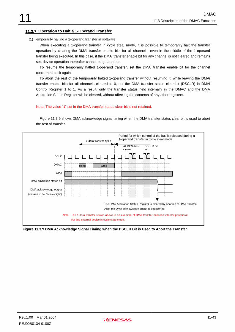
DMAC 11.3 Description of the DMAC Functions
Rev.1.00 Mar 01,2004 11-43
REJ09B0134-0100Z
11 11.3.7 Operation to Halt a 1-Operand Transfer
(1) Temporarily halting a 1-operand transfer in software
When executing a 1-operand transfer in cycle steal mode, it is possible to temporarily halt the transfer operation by clearing the DMAi transfer enable bits for all channels, even in the middle of the 1-operand transfer being executed. In this case, if the DMAi transfer enable bit for any channel is not cleared and remains set, device operation thereafter cannot be guaranteed.
To resume the temporarily halted 1-operand transfer, set the DMAi transfer enable bit for the channel concerned back again.
To abort the rest of the temporarily halted 1-operand transfer without resuming it, while leaving the DMAi transfer enable bits for all channels cleared to 0, set the DMA transfer status clear bit (DSCLR) in DMAi Control Register 1 to 1. As a result, only the transfer status held internally in the DMAC and the DMA Arbitration Status Register will be cleared, without affecting the contents of any other registers.
Note: The value “1” set in the DMA transfer status clear bit is not retained.
Figure 11.3.9 shows DMA acknowledge signal timing when the DMA transfer status clear bit is used to abort
the rest of transfer.
All DENi bits cleared
DSCLR bit set
1-data transfer cycle
Period for which control of the bus is released during a 1-operand transfer in cycle steal mode
The DMA Arbitration Status Register is cleared by abortion of DMA transfer.
Also, the DMA acknowledge output is deasserted.
Note: The 1-data transfer shown above is an example of DMA transfer between internal peripheral
I/O and external device in cycle steal mode.
Read Write
BCLK
DMAC
CPU
DMA arbitration status bit
DMA acknowledge output
(chosen to be “active-high”)
Figure 11.3.9 DMA Acknowledge Signal Timing when the DSCLR Bit is Used to Abort the Transfer

DMAC 11.3 Description of the DMAC Functions
Rev.1.00 Mar 01,2004 11-44
REJ09B0134-0100Z
11 11.3.8 Transfer Rate
The following shows an example of how to calculate the transfer rate. Calculation conditions
DMA transfer mode: Burst mode Transfer unit: Address aligned 32-bit data or 16-bit data Operating clock: 100 MHz External device wait cyclesNote: Zero wait during read, zero wait during write
Maximum transfer rate for internal peripheral I/O (internal memory) → internal peripheral I/O (internal memory)
× 4 (bytes) = 200 Mbytes/sec
Maximum transfer rate for internal peripheral I/O (internal memory) → external device
× 2 (bytes) = 40 Mbytes/sec
Maximum transfer rate for external device → internal peripheral I/O (internal memory)
× 2 (bytes) = 40 Mbytes/sec
Maximum transfer rate for external device → external device
× 2 (bytes) = 28.5 Mbytes/sec
100MHz 1 [read] + 1 [write]
100MHz 1 [read] + 3 [write] + 1 [idle]
100MHz 2 [read] + 1 [write] + 2 [idle]
100MHz 2 [read] + 3 [write] + 2 [idle]
Note: The number of wait cycles to be inserted for external devices are set by using the BSEL control registers. For
details, refer to Chapter 9, “External Bus Interface.”

DMAC 11.3 Description of the DMAC Functions
Rev.1.00 Mar 01,2004 11-45
REJ09B0134-0100Z
11 11.3.9 Example Initialization of the DMAC Related Registers
The following shows an example of how to initialize the DMAC related registers.
(1) DMAi Control Register 0
(2) DMAi Control Register 1
(3) DMAi Current Source Address Register
(4) DMAi Reload Source Address Register
... when using the reload function
(5) DMAi Current Destination Address Register
(6) DMAi Reload Destination Address Register
.... when using the reload function
(7) DMAi Current Byte Count Register
(8) DMAi Reload Byte Count Register
.... when using the reload function
(9) DMAi Interrupt Control Register
.... when using an interrupt
(10) DMA transfer enable bit
Setup sequence

DMAC 11.4 Example DMAC Settings
Rev.1.00 Mar 01,2004 11-46
REJ09B0134-0100Z
11 11.4 Example DMAC Settings
Figure 11.4.1 through Figure 11.4.3 show example DMAC settings.
Example DMA setting 1 SDRAM → user IP module, fly-by transfer
DMA Fly-by Transfer Latency Register 0 1 2 3 4 5 6 7 8 9 10 11 12 13 14 15 0 0 0 0 0 0 0 0 0 0 0 0 0 0 0 0
16 17 18 19 20 21 22 23 24 25 26 27 28 29 30 31
FBRL FBWL 0 0 0 0 0 0 0 1 0 0 0 0 0 1 0 1
DMAi Control Register 0 0 1 2 3 4 5 6 7 8 9 10 11 12 13 14 15
DREQ SZSEL MDSEL DIRQ DSEL OPSEL ALSEL BRLOD SRLOD DRLOD0 0 1 0 0 0 0 0 0 0 1 0 0 0 0 0
16 17 18 19 20 21 22 23 24 25 26 27 28 29 30 31SAMOD DAMOD FB TDIR DSE REQSEL
0 1 0 0 1 1 1 1 0 0 0 0 0 0 1 0
ACT DSL RD RD RD RD PRA DSL
BCLK
DREQ
DACK
FBMODE
FBRS
FBWS
D0–D31
SDRAM commands
FBWL
FBWL = 5 CLKs SZSEL = ‘10’ (word) MDSEL = ‘0’ (bus control continuously retained
mode) DSEL = ‘0’ (until 1-operand transfer finishes) OPSEL = ‘010’ (4 data) SAMOD = ‘01’ (increment) DAMOD = Has no effect when FB = 1 FB = ‘1’ (fly-by transfer) TDIR = ‘111’ (SDRAM → user IP module) REQSEL = ‘00010’ (user IP module)
Figure 11.4.1 Example DMA Setting 1

DMAC 11.4 Example DMAC Settings
Rev.1.00 Mar 01,2004 11-47
REJ09B0134-0100Z
11
Example DMA setting 2 SDRAM → external I/O device, dual-address transfer
DMAi Control Register 0 0 1 2 3 4 5 6 7 8 9 10 11 12 13 14 15
DREQ SZSEL MDSEL DIRQ DSEL OPSEL ALSEL BRLOD SRLOD DRLOD0 0 1 0 0 0 0 0 0 0 0 1 0 0 0 0
16 17 18 19 20 21 22 23 24 25 26 27 28 29 30 31SAMOD DAMOD FB TDIR DSE REQSEL
0 1 0 1 0 0 1 1 0 0 0 0 0 0 0 1
ACT DSL RD PRA DSL
BCLK
DREQ
A8–A30
BSEL#
WS#
D0–D31
SDRAM commands
SDRAM access Idle External access Idle
ACT DSL
SDRAM access
RD PRA DSL
Idle External access
SZSEL = ‘10’ (word) MDSEL = ‘0’ (bus control continuously retained
mode) DSEL = ‘0’ (until 1-operand transfer finishes) OPSEL = ‘001’ (2 data) SAMOD = ‘01’ (increment) DAMOD = ‘01’ (increment) FB = ‘0’ (dual-address transfer) TDIR = ‘011’ (external → external) REQSEL:" REQSEL = ‘00001’ (external device)
Figure 11.4.2 Example DMA Setting 2

DMAC 11.4 Example DMAC Settings
Rev.1.00 Mar 01,2004 11-48
REJ09B0134-0100Z
11
Example DMA setting 3 External I/O device → SDRAM via internal SRAM, dual-address transfer
DMA0 Control Register 0 0 1 2 3 4 5 6 7 8 9 10 11 12 13 14 15
DREQ SZSEL MDSEL DIRQ DSEL OPSEL ALSEL BRLOD SRLOD DRLOD0 0 1 0 0 0 0 0 0 0 0 1 0 0 0 0
16 17 18 19 20 21 22 23 24 25 26 27 28 29 30 31SAMOD DAMOD FB TDIR DSE REQSEL
0 1 0 1 0 0 1 0 0 0 0 0 0 0 0 1
DMA1 Control Register 0 0 1 2 3 4 5 6 7 8 9 10 11 12 13 14 15
DREQ SZSEL MDSEL DIRQ DSEL OPSEL ALSEL BRLOD SRLOD DRLOD0 0 1 0 0 0 0 0 0 0 0 1 0 0 0 0
16 17 18 19 20 21 22 23 24 25 26 27 28 29 30 31SAMOD DAMOD FB TDIR DSE REQSEL
0 1 0 1 0 0 0 1 0 0 0 0 0 0 0 1
BCLK
DREQ
A8–A30
BSEL#
RS#
D0–D31
SDRAM commands ACT DSL WR PRA DSL WR
External I/O access Idle SDRAM access
Internal statusTransfer write Transfer write Read
Idle
Read
Channel 0 transfer Channel 1 transfer
DMA channel 0 (external I/O → internal SRAM) SZSEL = ‘10’ (word) MDSEL = ‘0’ (bus control continuously
retained mode) DSEL = ‘0’ (until 1-operand transfer finishes) OPSEL = ‘001’ (2 data) SAMOD/DAMOD = ‘01’ (increment) FB = ‘0’ (dual-address transfer) TDIR = ‘010’ (external device → internal
resource) REQSEL = ‘00001’ (external device)
DMA channel 1 (internal SRAM → SDRAM)
SZSEL = ‘10’ (word) MDSEL = ‘0’ (bus control continuously
retained mode) DSEL = ‘0’ (until 1-operand transfer finishes) OPSEL = ‘001’ (2 data) SAMOD/DAMOD = ‘01’ (increment) FB = ‘0’ (dual-address transfer) TDIR = ‘010’ (internal resource → external
device) REQSEL = ‘00001’ (external device)
Figure 11.4.3 Example DMA Setting 3

DMAC 11.5 Precautions about the DMAC
Rev.1.00 Mar 01,2004 11-49
REJ09B0134-0100Z
11 11.5 Precautions about the DMAC
1. If other than software trigger is selected by the DMA request source select bits (REQSEL) in DMAi Control Register 0, do not set the DMA request bit (DREQ) in DMAi Control Register 0 by writing 1 in software. If this bit is set to 1 in this case, device operation thereafter cannot be guaranteed.
2. If the transfer data size select bits (SZSEL) in DMAi Control Register 0 are set to "8 bits," make sure the values set in the DMA Current Byte Count and DMA Reload Byte Count Registers are integer multiples of the number of transfer data that is selected by the 1-operand transfer data quantity select bits (OPSEL) in DMAi Control Register 0. Furthermore, if the transfer data size select bits are set to “16 bits” or “32 bits,” make sure the set values of the DMA current and reload byte counts are even multiples of or multiples of 4 times the number of transfer data selected with the 1-operand transfer data quantity select bits, respectively. If any other value than that is set, device operation cannot be guaranteed. When the transfer data size = 8 bits, integer multiple of the number of data in a 1-operand transfer (e.g.,
x1, x2 and so on) When the transfer data size = 16 bits, even multiple of the number of data in a 1-operand transfer (e.g.,
x2, x4 and so on) When the transfer data size = 32 bits, multiple of 4 times the number of data in a 1-operand transfer
(e.g., x4, x8 and so on) 3. If the DMAi Current Source Address Register is accessed for write in the middle of a 1-operand transfer,
device operation cannot be guaranteed. 4. If the DMAi Current Destination Address Register is accessed for write in the middle of a 1-operand transfer,
device operation cannot be guaranteed. 5. If the DMAi Current Byte Count Register is accessed for write in the middle of a 1-operand transfer, device
operation cannot be guaranteed. 6. The DMAi Current Source Address Register, DMAi Reload Source Address Register, DMAi Current
Destination Address Register and DMAi Reload Destination Address Register-all of these four registers should be set in such a way that DMA transfer is performed within the address boundary aligned to the transfer data size that was selected by the transfer data size select bits (SZSEL) in DMAi Control Register 0. If any other value than that is set, device operation cannot be guaranteed.
7. To temporarily halt the 1-operand transfer being executed in cycle steal mode, clear the DMAi transfer enable bits (DEN) for all channels. If the DMAi transfer enable bit for any channel other than the currently halted channel remains set, device operation thereafter cannot be guaranteed.
8. While the DMAi transfer enable bit (DEN) for any channel is set to 1, do not set the DMA transfer status clear bit (DSCLR) in DMAi Control Register 1. If this bit is set by writing 1, device operation thereafter cannot be guaranteed. Also be aware that although the DMA transfer status clear bit is provided for each channel, it works for all channels in common. Therefore, if the DMA transfer status clear bit for whichever channel is set by writing 1, a temporarily halted DMA transfer, if any, is aborted.

DMAC 11.5 Precautions about the DMAC
Rev.1.00 Mar 01,2004 11-50
REJ09B0134-0100Z
11
This page is blank for reasons of layout.

CHAPTER 12MULTIFUNCTION TIMER (MFT) CHAPTER 12
MULTIFUNCTION TIMER (MFT)

MULTIFUNCTION TIMER (MFT) 12.1 Outline of the Multifunction Timer
Rev.1.00 Mar 01,2004 12-2
REJ09B0134-0100Z
12 12.1 Outline of the Multifunction Timer
The multifunction timer can be used as timers/counters that have the following functions.
Output related timers
Fixed period timer
PWM waveform output timer
One-shot timer
Real port timer
Input related timers
Period/pulse width measurement timer
1-phase event counter
2-phase event counter
Figure 12.1.1 shows a configuration of MFTs. Figure 12.1.2 shows a basic block diagram of MFTs. Figure 12.1.3
shows the function of each MFT pin when the MFT is set in basic mode. Note that MFTi in this chapter denotes i = 0–5.
MFT0
Co
ntr
ol
Cir
cuit
TA0TB0 TB0
MFT1
MFT2
MFT3
TA1TB1 TB1
TA2TB2 TB2
TA3TB3 TB3
TA4TB4 TB4
TA5TB5 TB5
MFT4
MFT5
Figure 12.1.1 Configuration of the MFT
Comparison output
16-bit MFT compare reload register Real port register
Interrupt request
DMA request
TBi pin
Terminal count
MFT block
TAi pin
Count source
PCLK
Gate/trigger input Count source input Measured waveform input 2-phase event A input
1-phase event input 2-phase event B input Count source input
Waveform output Real port output
TBi pin
Not dividedDivided by 8
Divided by 32Divided by 128
Edge processing and trigger processing
16-bit MFT counter
Output proc-essing
Interrupt processing
16-bit MFT reload register
16-bit MFT compare register
Figure 12.1.2 Basic Block Diagram of the MFT

MULTIFUNCTION TIMER (MFT) 12.1 Outline of the Multifunction Timer
Rev.1.00 Mar 01,2004 12-3
REJ09B0134-0100Z
12
TAi pin
TBi pin TBi pin
Interrupt request DMA request
MFT
MFTi block
Gate/trigger input Count source input Measured waveform input 2-phase event A input
1-phase event input 2-phase event B input Count source input
Waveform output Real port output
Output Related Input Related Basic Mode
Pin Name
Fixed period timer
PWM waveform output timer One-shot timer Real port
timer Period/pulse width measurement timer
1-phase event counter
2-phase event counter
TAi pin Input Gate/trigger input or count source input
Gate/trigger input or count source input
Gate/trigger input or count source input
Measured waveform input Gate/trigger input
2-phase event A input
TBi pin Input Count source input 1-phase event input
2-phase event B input
TBi pin Output Waveform output Waveform output Waveform output
Real port output
Figure 12.1.3 MFT Modes and Pin Functions

MULTIFUNCTION TIMER (MFT) 12.2 Multifunction Timer Related Registers
Rev.1.00 Mar 01,2004 12-4
REJ09B0134-0100Z
12 12.2 Multifunction Timer Related Registers
The following describes a memory map associated with the multifunction timer and each related register. Multifunction Timer Register Mapping 1
Address b0 +0 address
b7 b8 +1 address
b15 b16 +2 address
b23 b24 +3 address
b31H'00EF C000 MFT Control Register
(MFTCR) H'00EF C004 MFT Real Port Register
(MFTRPR)
~ (Use of this area prohibited)
H'00EF C100 MFT0 Mode Register (MFT0MOD)
H'00EF C104 MFT0 Pin Output Status Register (MFT0OS)
H'00EF C108 MFT0 Counter (MFT0CUT)
H'00EF C10C MFT0 Reload Register (MFT0RLD)
H'00EF C110 MFT0 Compare Reload Register (MFT0CMPRLD)
~ (Use of this area prohibited)
H'00EF C200 MFT1 Mode Register (MFT1MOD)
H'00EF C204 MFT1 Pin Output Status Register (MFT1OS)
H'00EF C208 MFT1 Counter (MFT1CUT)
H'00EF C20C MFT1 Reload Register (MFT1RLD)
H'00EF C210 MFT1 Compare Reload Register (MFT1CMPRLD)
~ (Use of this area prohibited)
H'00EF C300 MFT2 Mode Register (MFT1MOD)
H'00EF C304 MFT2 Pin Output Status Register (MFT1OS)
H'00EF C308 MFT2 Counter (MFT2CUT)
H'00EF C30C MFT2 Reload Register (MFT2RLD)
H'00EF C310 MFT2 Compare Reload Register (MFT2CMPRLD)
~ (Use of this area prohibited)

MULTIFUNCTION TIMER (MFT) 12.2 Multifunction Timer Related Registers
Rev.1.00 Mar 01,2004 12-5
REJ09B0134-0100Z
12 Multifunction Timer Register Mapping 2
Address b0 +0 address
b7 b8 +1 address b1 b16
+2 addressb23 b24
+3 address b31
H'00EF C400 MFT3 Mode Register (MFT3MOD)
H'00EF C404 MFT3 Pin Output Status Register (MFT3OS)
H'00EF C408 MFT3 Counter (MFT3CUT)
H'00EF C40C MFT3 Reload Register (MFT3RLD)
H'00EF C410 MFT3 Compare Reload Register (MFT3CMPRLD)
~ (Use of this area prohibited)
H'00EF C500 MFT4 Mode Register (MFT4MOD)
H'00EF C504 MFT4 Pin Output Status Register (MFT14S)
H'00EF C508 MFT4 Counter (MFT4CUT)
H'00EF C50C MFT4 Reload Register (MFT4RLD)
H'00EF C510 MFT4 Compare Reload Register (MFT4CMPRLD)
~ (Use of this area prohibited)
H'00EF C600 MFT5 Mode Register (MFT5MOD)
H'00EF C604 MFT5 Pin Output Status Register (MFT5OS)
H'00EF C608 MFT5 Counter (MFT5CUT)
H'00EF C60C MFT5 Reload Register (MFT5RLD)
H'00EF C610 MFT5 Compare Reload Register (MFT5CMPRLD)

MULTIFUNCTION TIMER (MFT) 12.2 Multifunction Timer Related Registers
Rev.1.00 Mar 01,2004 12-6
REJ09B0134-0100Z
12 12.2.1 MFT Control Register
MFT Control Register (MFTCR) <Address: H’00EF C000>
b0 1 2 3 4 5 6 7 8 9 10 11 12 13 14 b15
0 0 0 0 0 0 0 0 0 0 0 0 0 0 0 0
b16 17 18 19 20 21 22 23 24 25 26 27 28 29 30 b31
MFT0MSK MFT1MSK MFT2MSK MFT3MSK MF4MSK MFT5MSK MFT0EN MFT1EN MFT2EN MFT3EN MFT4EN MFT5EN 0 0 0 0 0 0 0 0 0 0 0 0 0 0 0 0
<After reset: H’0000 0000>
b Bit Name Function R W
0–15 No functions assigned. Fix these bits to 0. 0 0
16 MFT0MSK MFT0EN write mask bit
0: Write to MFT0EN masked 1: Write to MFT0EN unmasked
0 *
17 MFT1MSK MFT1EN write mask bit
0: Write to MFT1EN masked 1: Write to MFT1EN unmasked
0 *
18 MFT2MSK MFT2EN write mask bit
0: Write to MFT2EN masked 1: Write to MFT2EN unmasked
0 *
19 MFT3MSK MFT3EN write mask bit
0: Write to MFT3EN masked 1: Write to MFT3EN unmasked
0 *
20 MFT4MSK MFT4EN write mask bit
0: Write to MFT4EN masked 1: Write to MFT4EN unmasked
0 *
21 MFT5MSK MFT5EN write mask bit
0: Write to MFT5EN masked 1: Write to MFT5EN unmasked
0 *
22–23 No functions assigned. Fix these bits to 0. 0 0
24 MFT0EN MFT0 enable bit
0: Stops MFT0 1: Enable MFT0 operation
R W
25 MFT1EN MFT1 enable bit
0: Stops MFT1 1: Enable MFT1 operation
R W
26 MFT2EN MFT2 enable bit
0: Stops MFT2 1: Enable MFT2 operation
R W
27 MFT3EN MFT3 enable bit
0: Stops MFT3 1: Enable MFT3 operation
R W
28 MFT4EN MFT4 enable bit
0: Stops MFT4 1: Enable MFT4 operation
R W
29 MFT5EN MFT5 enable bit
0: Stops MFT5 1: Enable MFT5 operation
R W
30–31 No functions assigned. Fix these bits to 0. 0 0
Note: The asterisk (*) in the W column denotes that writing 0 has no effect, and that data “1” written to the bit is not retained.

MULTIFUNCTION TIMER (MFT) 12.2 Multifunction Timer Related Registers
Rev.1.00 Mar 01,2004 12-7
REJ09B0134-0100Z
12 (1) MFTiMSK (MFTiEN write mask) bits (b16–b21)
These bits control masking write to the MFTi enable bit (MFTiEN). If when the MFTi enable bit is accessed for write, the corresponding MFTiMSK bit is found cleared to 0, no
data is written to the MFTi enable bit. If when the MFTi enable bit is accessed for write, the corresponding MFTiMSK bit is found set to 1, write to the MFTi enable bit is enabled and its value can be altered.
The value “1” written to this bit is not retained. Therefore, make sure this bit is set to 1 each time the MFTi enable bit is accessed for write.
(2) MFTiEN (MFTi enable) bits (b24–b29)
These bits enable or disable MFTi operation. Setting this bit to 1 enables MFTi operation. Clearing this bit to 0 stops MFTi. When stopped, the MFTi
Counter retains its value, so that when this bit is set to 1 to restart MFTi, the counter starts counting from the retained value.
Reading this bit helps to know whether the timer operation is enabled or has been stopped. This bit is automatically cleared to 0 when all of the following conditions are met. When MFTi is used as an output related timer (when MFTi Mode Register TSEL bit = 1) When trigger input is selected with the gate polarity/trigger select bit (Output Related MFTi Mode Register
GTSEL bits) When the terminal counts select bit (Output Related MFTi Mode Register TCSEL bit) is set to “once” When the next active edge of the input count source occurs after the terminal count is reached
Note 1: The clock divider that generates the count source is used in common by each MFT. This means that
the clock divider is not always initialized when MFTi starts. Therefore, for a while before MFTi actually starts counting or outputs a waveform after operation, the period (resolution) of the selected count source includes some hardware indeterminacy, as shown below.
Note 2: The timing at which MFTi starts counting is different between the input related and output related timers.
Note 3: The count source cannot be observed from the outside.
Figure 12.2.1 shows MFTi startup timing.
Count source
MFTi enable bit
TAi pin input (rising edgesensitive or active high)
TBi pin (waveform output)
Input related timerstarts counting
Output related timerstarts counting(1)
(2)
Output operation starts
Enable timer
Hardware indeterminacy(1) When gate/trigger input is
disabled: From assertion ofthe MFTi enable bit to thecount source
(2) When gate/trigger input isenabled: From active edge orlevel to the count source afterthe MFTi enable bit is set
Figure 12.2.1 MFTi Startup Timing

MULTIFUNCTION TIMER (MFT) 12.2 Multifunction Timer Related Registers
Rev.1.00 Mar 01,2004 12-8
REJ09B0134-0100Z
12 12.2.2 MFT Real Port Register
MFT Real Port Register (MFTRPR) <Address: H’00EF C004>
b0 1 2 3 4 5 6 7 8 9 10 11 12 13 14 b15
0 0 0 0 0 0 0 0 0 0 0 0 0 0 0 0
b16 17 18 19 20 21 22 23 24 25 26 27 28 29 30 b31
MT0D MT1D MT2D MT3D MT4D MT5D 0 0 0 0 0 0 0 0 0 0 0 0 0 0 0 0
<After reset: H’0000 0000>
b Bit Name Function R W
0–15 No functions assigned. Fix these bits to 0. 0 0
16 MT0D MFT real port data bit
0: Output a low from TB0 pin 1: Output a high from TB0 pin
R W
17 MT1D MFT1 real port data bit
0: Output a low from TB1 pin 1: Output a high from TB1 pin
R W
18 MT2D MFT2 real port data bit
0: Output a low from TB2 pin 1: Output a high from TB2 pin
R W
19 MT3D MFT3 real port data bit
0: Output a low from TB3 pin 1: Output a high from TB3 pin
R W
20 MT4D MFT4 real port data bit
0: Output a low from TB4 pin 1: Output a high from TB4 pin
R W
21 MT5D MFT5 real port data bit
0: Output a low from TB5 pin 1: Output a high from TB5 pin
R W
22–31 No functions assigned. Fix these bits to 0. 0 0
The MFT Real Port Register is used to set the data that can be output from the timer output pin when MFTi is set
for real port output mode (Output Related MFTi Mode Register TOSEL bits = ‘11’). The value set in the MFT Real Port Register is reflected in the output pin at the next active edge of the input count
source after the terminal count is reached. The real port output value is not affected by the MFTi enable bit (MFTiEN) in the MFT Control Register. Figure 12.2.2 shows example real port output.
MFTi enable bit
Count source
MFTi counter
TBi pin output
Note 1: The output value is not affected by the MFTi enable bit.Note 2: If the TBi Pin Output Status Register is rewritten while the MFTi enable bit remainscleared to 0 after the report port register value was reflected in the output pin, the value of the pinoutput status bit will be reflected in the output pin again.
Value of the pin output status bit
Enable bit set to 1Enable bit cleared to 0Enable bit set to 1
"H'0000"
Value written to the correspondingbit in the MFTi Real Port Register
Figure 12.2.2 Example Real Port Output

MULTIFUNCTION TIMER (MFT) 12.2 Multifunction Timer Related Registers
Rev.1.00 Mar 01,2004 12-9
REJ09B0134-0100Z
12 12.2.3 MFTi Mode Register
The MFTi Mode Register has a timer select bit (TSEL) that is used to select MFTi between an output related timer and an input related timer. The contents of the register bits vary depending on which timer function is selected.
The MFTi Mode Register is described in order of the following:
(1) MFTi Mode Register when used as output related
(2) MFTi Mode Register when used as input related
Note 1: The MFTi Mode Register cannot be rewritten during timer operation. Before resetting it, be sure to check
the MFTi enable bit (MFT Control Register MFTiEN bit) to see that the timer has stopped and currently is idle.
(1) MFTi Mode Register when used as output related
Setting the timer select bit (TSEL) in the MFTi Mode Register to 1 allows to use MFTi as an output related timer. In this case, the MFTi Mode Register operates as a register for the output related timer.
Output Related MFT0 Mode Register (MFT0MOD) <Address: H’00EF C100>
Output Related MFT1 Mode Register (MFT1MOD) <Address: H’00EF C200>
Output Related MFT2 Mode Register (MFT2MOD) <Address: H’00EF C300>
Output Related MFT3 Mode Register (MFT3MOD) <Address: H’00EF C400>
Output Related MFT4 Mode Register (MFT4MOD) <Address: H’00EF C500>
Output Related MFT5 Mode Register (MFT5MOD) <Address: H’00EF C600>
b0 1 2 3 4 5 6 7 8 9 10 11 12 13 14 b15
0 0 0 0 0 0 0 0 0 0 0 0 0 0 0 0
b16 17 18 19 20 21 22 23 24 25 26 27 28 29 30 b31
TSEL TCSEL TCCR TOSEL GTSEL OLSEL CMSEL CSSEL 0 0 0 0 0 0 0 0 0 0 0 0 0 0 0 0
<After reset: H’0000 0000>
b Bit Name Function R W
0–15 No functions assigned. Fix these bits to 0. 0 0
16 TSEL Timer select bit
1: Output related timer 1 1
17 TCSEL Terminal counts select bit
0: Unlimited 1: Once
R W
18 TCCR Terminal count control bit
0: MFTi Counter = H’0000 or H’FFFF 1: MFTi Counter ≥ MFTi Compare Register
MFTi Counter < MFTi Compare Register
R W
19–20 TOSEL[0:1]
Timer output select bits 00: No output 01: waveform output 10: Toggle waveform output 11: Real port output
R W

MULTIFUNCTION TIMER (MFT) 12.2 Multifunction Timer Related Registers
Rev.1.00 Mar 01,2004 12-10
REJ09B0134-0100Z
12 21–23 GTSEL
Gate polarity/trigger select bits 000: Gate/trigger input disabled 001: Trigger input (rising edge) 010: Trigger input (falling edge) 011: Trigger input (both edges) 100: Setting prohibited 101: Setting prohibited 110: Gate input (active when low) 111: Gate input (active when high)
R W
24–26 No functions assigned. Fix these bits to 0. 0 0
27 OLSEL Output level select bit
0: Positive 1: Negative
R W
28 CMSEL Count mode select bit
0: Down count 1: Up count
R W
29–31 CSSEL Count source select bits
000: PCLK (peripheral I/O clock) 001: PCLK (peripheral I/O clock)/8 010: PCLK (peripheral I/O clock)/32 011: PCLK (peripheral I/O clock)/128 100: Setting prohibited 101: Setting prohibited 110: TAi count source input 111: Setting prohibited
R W
(1) TSEL (timer select) bit (b16)
This bit selects to use MFTi as an output related timer or an input related timer. Clearing this bit to 0 allows to use MFTi as an input related timer, and setting this bit to 1 allows to use MFTi as
an output related timer. For operation of the input related timer, refer to paragraph (2), “MFTi Mode Register when used as input related,” described later.
(2) TCSEL (terminal counts select) bit (b17)
This bit selects whether or not to automatically clear the MFTi enable bit (MFTiEN) in the MFT Control Register after the terminal count is reached.
When this bit is cleared to 0, the MFTi enable bit is not cleared at the next active edge of the input count source after the terminal count is reached, allowing MFTi to continue operating.
When this bit is set to 1, the MFTi enable bit is cleared at the next active edge of the input count source after the terminal count is reached (refer to the TCCR bit described later). Even in this case, however, if trigger input from the TAi pin is enabled by the gate polarity/trigger select bits (GTSEL = ‘001,’ ‘010’ or ‘011’), the MFTi enable bit is not cleared even after the terminal count is reached.
(3) TCCR (terminal count control) bit (b18)
This bit allows to set conditions under which the terminal count signal is generated (terminal count is an internal control signal).
When this bit is cleared to 0, the terminal count signal is generated when MFTi Counter value = H’FFFF (during up-count) MFTi Counter value = H’0000 (during down-count) For details about up-count and down-count, refer to the count mode select bit (CMSEL) described below. Figure 12.2.3 shows an example of when the terminal count signal is generated if this bit is set to 0.

MULTIFUNCTION TIMER (MFT) 12.2 Multifunction Timer Related Registers
Rev.1.00 Mar 01,2004 12-11
REJ09B0134-0100Z
12 During up-count
Count source
MFTi Counter
MFTi Counter
Reloaded,automaticallycleared, etc.
"H'FFFF"
During down-count
"H'0000"
Terminal count(internal control
signal)
Terminal count(internal control
signal)
Count source
Reloaded,automatically cleared,
etc. Figure 12.2.3 Example of When Terminal Count Signal is Generated if TCCR = 0
If this bit is set to 1, the terminal count signal is generated when MFTi Counter value ≥ MFTi Compare Register value (during up-count) MFTi Counter value < MFTi Compare Register value (during down-count) Note
Use the count mode select bit (CMSEL) to select between up-count and down-count.
Note: It is only when all of the following conditions are met that the terminal count signal is generated when MFTi Counter value ≤ MFTi Compare Register value (during up-count).
The terminal count control bit (TCCR) = 1 Down-count is selected by the count mode select bit (CMSEL = 1) MFTi Compare Register value = H’0000
Figure 12.2.4 shows an example of when the terminal count signal is generated if this bit is set to 1.
During up-count
Count source
MFTi Counter
MFTi Counter
Reloaded, automaticallycleared, etc.
"H'FFFF"
During down-count
"H'0000"
Terminal count (internalcontrol signal)
Terminal count(internal control signal)
Count source
Area in which terminal count occursMFTi Compare Register
Area in which terminal count occurs
MFTi Compare Register
Reloaded, automaticallycleared, etc.
Figure 12.2.4 Example of When Terminal Count Signal is Generated If TCCR = 1

MULTIFUNCTION TIMER (MFT) 12.2 Multifunction Timer Related Registers
Rev.1.00 Mar 01,2004 12-12
REJ09B0134-0100Z
12 The following action occurs at the next active edge of the input count source after the terminal count is
reached: Reloading the MFTi Counter with the MFTi Reload Register value Generating an interrupt request to the ICU (Interrupt Controller) Generating a DMA request to the DMAC (DMA Controller) Automatically clearing the MFTi enable bit (MFTiEN) in the MFT Control Register (refer to the “terminal
counts select bit” described above) If toggle waveform output or real port output is selected (when TOSEL bits = ‘10’ or ‘11’), this bit should be
cleared to 0.

MULTIFUNCTION TIMER (MFT) 12.2 Multifunction Timer Related Registers
Rev.1.00 Mar 01,2004 12-13
REJ09B0134-0100Z
12 (4) TOSEL (timer output select) bits (b19, b20)
These bits allow to control the output from the TBi pin. When TOSEL = ‘01’ (comparison waveform output), the result derived by comparing the MFTi Counter value
and the MFTi Compare Register value is output as waveform from the TBi pin. For example output waveforms, refer to the description of the output level select bit (OLSEL) in paragraph (6), “OLSEL (output level select) bit”, described later.
When TOSEL = ‘10’ (toggle waveform output), the waveform output from the TBi pin is reversed each time the terminal count is reached. For example output waveforms, refer to the description of the output level select bit (OLSEL) in paragraph (6), “OLSEL (output level select) bit”, described later.
When TOSEL = ‘11’ (real port output), the MFT Real Port Register value output from the TBi pin. For example real port output, refer to Section 12.2.2, “MFT Real Port Register.”
If toggle waveform output or real port output is selected (when TOSEL bits = ‘10’ or ‘11’), the terminal count control bit (TCCR) should be fixed to 0.
If real port output is selected, the gate polarity/trigger select bits (GTSEL) should be fixed to ‘000’ (gate/trigger input has not effect).
If real port output is selected, setting the count source select bits (CSSEL) to ‘110’ (TAi count source input) is prohibited.
(5) GTSEL (gate polarity/trigger select) bits (b21–b23)
MFTi can be controlled (started or stopped) by an input signal to the TAi pin after setting the MFTi enable bit (MFT Control Register MFTiEN bit) to 1 to enable MFTi operation. These bits select to disable input (gate/trigger input) to the TAi pin or use it as gate input or trigger input.
<When gate/trigger input is disabled (GTSEL = ‘000’)>
When gate/trigger input is disabled, input to the TAi pin is ignored, and MFTi is started or stopped by only the MFTi enable bit. Note, however, that the MFTi Counter does not count on the first active edge of the input count source after MFTi operation is enabled. The MFTi Counter counts on all of the subsequent active edges of the input count source while MFTi operation is enabled.
Figure 12.2.5 shows an example count operation when gate/trigger input is disabled.
Note: The above output range applies to the case where comparison waveform output isselected by TOSEL.
MFTi enable bit
Value set in theMFTi Pin OutputStatus Register
(MFTiOS) is output
Counted
Count source
Result derived by comparing the MFTiCounter value and the MFTi Compare
Register value is output from the TBi pin
MFTi idle value selectedby the output levelselect bit (OLSEL) isoutput
Enable bit set to 1
MFTi operating
Not counted Counted
Figure 12.2.5 Example Count Operation when Gate/Trigger Input is Disabled

MULTIFUNCTION TIMER (MFT) 12.2 Multifunction Timer Related Registers
Rev.1.00 Mar 01,2004 12-14
REJ09B0134-0100Z
12 <When gate input is selected (GTSEL = ‘110’or ‘111’)>
When gate input is selected, MFTi operation is enabled only while MFTi enable bit (MFTiEN) = 1 and gate input on TAi pin is active. Note, however, that the MFTi Counter does not count on the first active edge of the input count source even while MFTi operation is enabled. The MFTi Counter counts on all of the subsequent active edges of the input count source while MFTi operation is enabled.
Figure 12.2.6 shows an example count operation when gate input is selected by GTSEL.
Note: The above output range applies to the case where comparison waveform output is selected by TOSEL.
MFTi enable bit
Value set in theMFTi Pin OutputStatus Register
(MFTiOS) is output
Counted
Count source
Result derived by comparing theMFTi Counter value and the MFTiCompare Register value is output
from the TBi pin
MFTi idle value selectedby the output levelselect bit (OLSEL) isoutput
Enable bit set to 1
MFTi operating
Not counted
TAi pin input (chosento be active-high)
Figure 12.2.6 Example Count Operation when Gate Input is Selected
<When trigger input is selected (GTSEL = ‘001,’ ‘010’ or ‘011’)>
When trigger input is selected, MFTi operation is enabled when MFTi enable bit (MFTiEN) = 1 and an active edge of the trigger input on TAi pin is detected. Note, however, that the MFTi Counter does not count on the first active edge of the input count source even while MFTi operation is enabled. The MFTi Counter counts on all of the subsequent active edges of the input count source while MFTi operation is enabled. Although trigger input is ignored once MFTi operation has been enabled, if the terminal count control bit (TCCR) in the Output Related MFTi Mode Register is set to 1, the counter stops counting after the terminal count is reached and waits for trigger input again.
Figure 12.2.7 shows an example count operation when trigger input is selected by GTSEL.
Note: The above output range applies to the case where comparison waveform output is selected by TOSEL.
MFTi enable bit
Value set in the MFTi PinOutput Status Register
(MFTiOS) is output
Counted
Count source
Result derived by comparingthe MFTi Counter value andthe MFTi Compare Register
value is output from the TBi pin
MFTi idle value selectedby the output level selectbit (OLSEL) is output
Enable bit set to 1
MFTi operating
Not counted
TAi pin input(chosen to be rising
edge sensitive)
Figure 12.2.7 Example Count Operation when Trigger Input is Selected

MULTIFUNCTION TIMER (MFT) 12.2 Multifunction Timer Related Registers
Rev.1.00 Mar 01,2004 12-15
REJ09B0134-0100Z
12 Furthermore, if the TAi pin is set for count source input rather than for gate/trigger input by the count source
select bits (CSSEL), set GTSEL = ‘001,’ ‘010’ or ‘011’ to select the active edge of the count source. Table 12.2.1 lists the functions of the gate polarity/trigger select bits (GTSEL).
Table 12.2.1 Functions of the Gate Polarity/Trigger Select Bits
b21 b22 b23 Function Active Edge or Period
0 0 0 Gate/trigger input disabled
0 0 1 Trigger inputNote Rising edge
0 1 0 Falling edge
0 1 1 Both edges
1 0 0 Setting prohibited
1 0 1 Setting prohibited
1 1 0 Level input Active when low
1 1 1 Active when high
Note: When using the TAi pin for count source input as selected by the count source select bits (CSSEL), be sure to select trigger
input and its active edge.
(6) OLSEL (output level select) bit (b27)
This bit is effective only when comparison waveform output is selected by the timer output select bits (TOSEL = ‘01’).
This bit selects the polarity of output from the TBi pin to be positive (active-high) or negative (active-low) when it is output at the first active edge of the input count source after MFTi operation is enabled by the MFTi enable bit (MFTiEN) in the MFT Control Register. This bit also causes the comparison waveform output level to change when MFTi is stopped while operating. Note, however, that if this bit is altered while MFTi has been stopped by the MFTi enable bit, the changed state is not reflected in the output level until the first active edge of the input count source after MFTi operation is reenabled.
If this bit is cleared to 0, the polarity of output from the TBi pin is selected to be positive (active-high). In this case, the output level from the TBi pin becomes as follows:
<TBi pin output status when OLSEL = 0> When MFTi is stopped while operating, output level = low When MFTi Counter ≥ MFTi Compare Register, output level = high When MFTi Counter < MFTi Compare Register, output level = low
If this bit is set to 1, the polarity of output from the TBi pin is selected to be negative (active-low). In this case,
the output level from the TBi pin becomes as follows: <TBi pin output status when OLSEL = 1> When MFTi is stopped while operating, output level = high When MFTi Counter ≥ MFTi Compare Register, output level = low When MFTi Counter < MFTi Compare Register, output level = high
(7) CMSEL (count mode select) bit (b28)
This bit selects to use the MFTi Counter as a down-counter or as an up-counter. Clearing this bit to 0 allows to use the MFTi Counter as a down-counter. Setting bit to 1 allows to use the MFTi
Counter as an up-counter.
Figure 12.2.8 shows an example waveform output during up-count and down-count.

MULTIFUNCTION TIMER (MFT) 12.2 Multifunction Timer Related Registers
Rev.1.00 Mar 01,2004 12-16
REJ09B0134-0100Z
12
During up-count (gate/trigger input disabled)
Count source
MFTienable bit
During down-count (gate/trigger input disabled)
MFTi CompareRegister
<Comparison waveform output mode>
Enable bit set to 1
"H'FFFF"
(Note 1)
(Note 2)
Enable bit cleared to 0 Enable bit set to 1
MFTi Counter
TBi pin output(positive)
TBi pin output(negative)
Output turned onby MFTi invocation
Output turned on byMFTi re-invocation
Output turned off byclearing the enable bit to 0
Count source
MFTienable bit
MFTi CompareRegister
Enable bit set to 1
"H'0000"
(Note 1)
(Note 2)
Enable bit cleared to 0 Enable bit set to 1
MFTi Counter
TBi pin output(positive)
TBi pin output(negative)
Output turned onby MFTi invocation
Output turned on byMFTi re-invocation
Output turned off byclearing the enable bit to 0
During up-count (gate/trigger input disabled)
MFTi enablebit
<Comparison waveform output mode>
Enable bit set to 1 Enable bit cleared to 0 Enable bit set to 1
"H'FFFF"
Output started byterminal countgeneration
(Note 3)
(Note 1)
Count source
MFTi ReloadRegister
MFTi Counter
When MFTiBOS =0
When MFTiBOS =1
During down-count (gate/trigger input disabled)
MFTi enablebit
Enable bit set to 1 Enable bit cleared to 0 Enable bit set to 1
"H'0000"
Output started byterminal countgeneration
(Note 3)
(Note 1)
Count sourceMFTi Reload
RegisterMFTi Counter
When MFTiBOS= 0
When MFTiBOS= 1
Note 1: This indicates a period for which time the value written to the MFTi output status bit (MFTiOS) while MFTi remains
idle is reflected. The output value depends on the value of the TBi output status bit. Note 2: If the MFTi enable bit is cleared, the output data is immediately turned off. The output value while turned off is
determined by the output level select bit (OLSEL) Note 3: During toggle waveform output, the output value is not affected by the MFTi enable bit.
Figure 12.2.8 Example Waveform Output

MULTIFUNCTION TIMER (MFT) 12.2 Multifunction Timer Related Registers
Rev.1.00 Mar 01,2004 12-17
REJ09B0134-0100Z
12 (8) CSSEL (count source select) bits (b29-b31)
These bits select the count source for the MFTi Counter. If TAi count source input is selected with these bits, the active edge of the count source (TAi pin input) should be selected using the gate polarity/trigger select bits (GTSEL) from three choices available (rising edge, falling edge or both edges).
Figure12.2.9 shows an example MFTi operation when TAi count source input is selected for the count source (CSSEL = ‘110’).
MFTi enable bit
Counted
TAi pin input(chosen to be
rising edgesensitive)
||Used as the count
source
Enable bit set to 1
MFTi operating
Notcounted
Counted
Figure12.2.9 Example MFTi Operation when TAi Count Source Input is Selected
Table12.2.2 lists the functions of the count source select bits (CSSEL).
Table12.2.2 Functions of the Count Source Select Bits
Function b29 b30 b31
Count source
0 0 0 PCLK (peripheral I/O clock)
0 0 1 PCLK (peripheral I/O clock)/8
0 1 0 PCLK (peripheral I/O clock)/32
0 1 1 PCLK (peripheral I/O clock)/128
1 0 0 Setting prohibited
1 0 1 Setting prohibited
1 1 0 TAi count source inputNote 1
1 1 1 Setting prohibited
Note 1: When TAi count source input is selected, use the gate polarity/trigger select bits (GTSEL) to select trigger input and its active edge.

MULTIFUNCTION TIMER (MFT) 12.2 Multifunction Timer Related Registers
Rev.1.00 Mar 01,2004 12-18
REJ09B0134-0100Z
12 (2) MFTi Mode Register when used as input related
Clearing the timer select bit (TSEL) in the MFTi Mode Register to 0 allows to use MFTi as an input related timer. In this case, the MFTi Mode Register operates as a register for the input related timer.
Input Related MFT0 Mode Register (MFT0MOD) <Address: H’00EF C100>
Input Related MFT1 Mode Register (MFT1MOD)) <Address: H’00EF C200>
Input Related MFT2 Mode Register (MFT2MOD) <Address: H’00EF C300>
Input Related MFT3 Mode Register (MFT3MOD) <Address: H’00EF C400>
Input Related MFT4 Mode Register (MFT4MOD) <Address: H’00EF C500>
Input Related MFT5 Mode Register (MFT5MOD) <Address: H’00EF C600>
b0 1 2 3 4 5 6 7 8 9 10 11 12 13 14 b15
0 0 0 0 0 0 0 0 0 0 0 0 0 0 0 0
b16 17 18 19 20 21 22 23 24 25 26 27 28 29 30 b31
TSEL MSEL TCCR GTSEL MTMOD BWMSK UFFLG OFFLG CMSEL
ECSEL CSSEL
0 0 0 0 0 0 0 0 0 0 0 0 0 0 0 0
<After reset: H’0000 0000>
b Bit Name Function R W
0–15 No functions assigned. Fix these bits to 0. 0 0
16 TSEL Timer select bit
0: Input related timer 0 0
17 MSEL Operation mode select bit
0: 1-phase/2-phase event counter 1: Period/pulse width measurement timer
R W
18 TCCR Terminal count control bit
During 2-phase event counter mode Set this bit to 0. 0: MFTi Counter = H’0000 or H’FFFF 1: MFTi Counter = H’0000
MFTi Counter ≥ MFTi Compare Register
R W
19–20 No functions assigned. Fix these bits to 0. 0 0
21–23 <During 1-phase/2-phase event counter mode> GTSEL Gate polarity/trigger select bits
During 1-phase event counter mode 000: Gate/trigger input disabled 001: Trigger input (rising edge) 010: Trigger input (falling edge) 011: Trigger input (both edges) 100: Setting prohibited 101: Setting prohibited 110: Gate input (active when low) 111: Gate input (active when high)
During 2-phase event counter mode Set these bits to ‘000’.
R W

MULTIFUNCTION TIMER (MFT) 12.2 Multifunction Timer Related Registers
Rev.1.00 Mar 01,2004 12-19
REJ09B0134-0100Z
12 <During period/pulse width measurement
mode> MTMOD Measurement timer mode select bits
000: Setting prohibited 001: Period measurement (between rising edges) 010: Period measurement (between falling edges) 011: Pulse width measurement (rising edge → falling edge) (falling edge→ rising edge) 100: Setting prohibited 101: Setting prohibited 110: Setting prohibited 111: Setting prohibited
24 BWMSK b25, b26 write mask bit
0: Write to b25 and b26 masked 1: Write to b25 and b26 unmasked
R Note 1
25 UFFLG Underflow flag
0: No underflow 1: Underflowed
R Note 2
26 OFFLG Overflow flag
0: No overflow 1: Overflowed
R Note 2
27 No functions assigned. Fix this bit to 0. 0 0
28 CMSEL Count mode select bit
During 1-phase event counter mode 0: Down count 1: Up count
During 2-phase event counter mode 0: Standard mode 1: x4 mode
During period/pulse width measurement mode 1: Used as up count
R W
29–31 <During 1-phase/2-phase event counter mode> ECSEL Event counter mode select bits
000: 2-phase event counter 001: 1-phase event counter (rising edge) 010: 1-phase event counter (falling edge) 011: 1-phase event counter (both edges) 100: Setting prohibited 101: Setting prohibited 110: Setting prohibited 111: Setting prohibited
R W
<During period/pulse width measurement mode> CSSEL Count source select bits
000: PCLK (peripheral I/O clock) 001: PCLK (peripheral I/O clock)/8 010: PCLK (peripheral I/O clock)/32 011: PCLK (peripheral I/O clock)/128 100: Setting prohibited 101: Setting prohibited 110: Setting prohibited 111: TBi count source input
R W
Note 1: Writing 0 has no effect, and data “1” written to the bit is not retained.
Note 2: Writing to the flag independently of other bits has no effect. The flag is cleared by writing 0 simultaneously with bit 24 = 1,
and writing 1 simultaneously with bit 24 = 1 has no effect.

MULTIFUNCTION TIMER (MFT) 12.2 Multifunction Timer Related Registers
Rev.1.00 Mar 01,2004 12-20
REJ09B0134-0100Z
12 (1) TSEL (timer select) bit (b16)
This bit selects to use MFTi as an output related timer or an input related timer. When this bit is cleared to 0, MFTi operates as an input related timer. The input related timer may be used as
a period/pulse width measurement timer, 1-phase event counter or 2-phase event counter. When this bit is set to 1, MFTi operates as an output related timer. For details, refer to paragraph (1), “MFTi
Mode Register when used as output related,” described earlier.
(2) MSEL (operation mode select) bit (b17)
This bit selects 1-phase/2-phase event counter mode or period/pulse width measurement mode. When this bit is cleared to 0, MFTi operates in 1-phase/2-phase event counter mode. Use the event counter
mode select bit (ECSEL) to select between 1-phase and 2-phase event counter modes. During 1-phase event counter mode, MFTi counts on active edges of the input signal to the TBi pin. During 2-phase event counter mode, MFTi counts depending on the input status of the TAi and TBi pins.
When this bit is set to 1, MFTi operates in period/pulse width measurement mode. During period measurement timer mode, MFTi counts between rising edges or falling edges of the input signal to the TAi pin to measure the period. During pulse width measurement timer mode, MFTi counts from a rising edge to falling edge or from a falling edge to rising edge of the input signal to the TAi pin to measure the pulse width.
(3) TCCR (terminal count control) bit (b18)
This bit allows to set conditions under which the terminal count signal is generated (terminal count is an internal control signal).
When this bit is cleared to 0, the terminal count signal is generated when one of the following conditions is met: <When used as a period/pulse width measurement timer> When MFTi Counter value = H’FFFF
<When used as a 1-phase event counter> When MFTi Counter value = H’FFFF during up-count When MFTi Counter value = H’0000 during down-count
<When used as a 2-phase event counter> When MFTi Counter value overflows from H’FFFF to H’0000 during up-count When MFTi Counter value underflows from H’0000 to H’FFFF during down-count
For details about up-count and down-count, refer (8) CMSEL (counter mode select bit) described below. Figure 12.2.10 shows an example of when the terminal count signal is generated if this bit is set to 0.

MULTIFUNCTION TIMER (MFT) 12.2 Multifunction Timer Related Registers
Rev.1.00 Mar 01,2004 12-21
REJ09B0134-0100Z
12
During up-count (during 1-phase event counter or period/pulse width measurement mode>
Count source
MFTi Counter
MFTi Counter
Reloaded, etc.
"H'FFFF"
During down-count (during 1-phase event counter mode)Note
"H'0000"
Terminal count(internal control
signal)
Terminal count(internal control
signal) Reloaded, etc.
Count source
OFFLG bit
UFFLG bit
Note: Down-count cannot be selected during period/pulse width measurement mode.
During 2-phase event counter mode
"H'FFFF"
MFTi Counter
"H'0000"Terminal count(internal control
signal)
OFFLG bit
UFFLG bit
(Note)
(Note)
Up-count Down-count
Interrupt or DMA request is generated atthe same time the terminal count signalis generated.
Cleared in software
Cleared in software
Note:If the MFTi Counter neither overflows nor underflows at the next count after it reached H’0000 orH’FFFF, the terminal count signal is not generated, so is the interrupt or DMA request.
Figure 12.2.10 Example of When Terminal Count Signal is Generated if TCCR = 0

MULTIFUNCTION TIMER (MFT) 12.2 Multifunction Timer Related Registers
Rev.1.00 Mar 01,2004 12-22
REJ09B0134-0100Z
12 If this bit is set to 1, the terminal count signal is generated when one of the following conditions is met: When MFTi Counter value ≥ MFTi Compare Register value during up-count When MFTi Counter value = H’0000 during down-count
For details about up-count and down-count, refer (8) CMSEL (counter mode select bit) described below. Figure 12.2.11 shows an example of when the terminal count signal is generated if this bit is set to 1.
Note that the following action occurs at the next active edge of the input count source after the terminal count
is reached: Reloading the MFTi Counter with the MFTi Reload Register valueNote Generating an interrupt request to the ICU Generating a DMA request to the DMAC Setting the underflow flag (UFFLG) to 1 (only during 1-phase/2-phase event counter mode) Setting the overflow flag (OFFLG) to 1
Note: During 2-phase event counter mode, the terminal count control bit should be set to 0. In this case,
although the terminal count signal is generated when MFTi Counter value = H’FFFF or H’0000, the counter is not reloaded.
During up-count (during 1-phase event counter or period/pulse width measurement mode>
Count source
MFTi Counter
Reloaded, etc.
"H'FFFF"
Terminal count (internalcontrol signal)
OFFLG bit
Area in which terminal count occursMFTi Compare Register
Figure 12.2.11 Example of When Terminal Count Signal is Generated if TCCR = 1

MULTIFUNCTION TIMER (MFT) 12.2 Multifunction Timer Related Registers
Rev.1.00 Mar 01,2004 12-23
REJ09B0134-0100Z
12 (4) GTSEL or MTMOD (gate polarity/trigger select or measurement timer mode select) bits (b21–b23)
<During 1-phase/2-phase event counter mode> Gate polarity/trigger select bits
During 1-phase/2-phase event counter mode, MFTi can be controlled (started or stopped) by an input signal to the TAi pin after setting the MFTi enable bit (MFT Control Register MFTiEN bit) to 1 to enable MFTi operation. These bits (GTSEL) select to disable input (gate/trigger input) to the TAi pin or use it as gate input or trigger input.
During 1-phase event counter mode When GTSEL = ‘000’ (gate/trigger input disabled), input to the TAi pin is ignored, and MFTi is started or
stopped by only the MFTi enable bit. While MFTi operation is enabled (i.e., while MFTi is operating), all active edges (events) of the input signal
to the TBi pin are counted. Figure 12.2.12 shows an example count operation when gate/trigger input is disabled.
MFTi enable bit
Counted
TBi pin input(1-phase event
input)
Enable bit set to 1
MFTi operating
Counted Counted Figure 12.2.12 Example Count Operation when Gate/Trigger Input is Disabled
When GTSEL = ‘110’ or ‘111’ (gate input selected), MFTi operates only while the gate input on TAi pin is active
while MFTi operation is enabled, thereby counting active edges (events) of the input signal to the TBi pin. Figure 12.2.13 shows an example count operation when gate input is selected by GTSEL.
MFTi enable bit
Counted
TBi pin input (1-phase event input)
Enable bit set to 1
MFTi operating
Counted Counted
TAi pin input (chosento be active-high)
Figure 12.2.13 Example Count Operation when Gate Input is Selected

MULTIFUNCTION TIMER (MFT) 12.2 Multifunction Timer Related Registers
Rev.1.00 Mar 01,2004 12-24
REJ09B0134-0100Z
12 When GTSEL = ‘001’ or ‘010’ (trigger input selected), MFTi starts operating upon active edge (trigger) of the
input signal to the TAi pin after MFTi operation is enabled, thereby counting active edges (events) of the input signal to the TBi pin. Once MFTi operation is enabled, trigger input is ignored. To stop MFTi, clear the MFTi operation enable bit (MFTi Control Register MFTiEN bit).
Figure 12.2.14 shows an example count operation when trigger input is selected by GTSEL.
MFTi enable bit
Counted
TBi pin input (1-phaseevent input)
Enable bit set to 1
MFTi operating
Counted
TAi pin input (chosen tobe rising edge sensitive)
Figure 12.2.14 Example Count Operation when Trigger Input is Selected
During 2-phase event counter mode In this case, GTSEL should be set to ‘000’ (gate/trigger input disabled). Table 12.2.3 lists the functions of the gate polarity/trigger select bits (GTSEL).
Table 12.2.3 Functions of the Gate Polarity/Trigger Select Bits (1-phase/2-phase event counter mode)
b21 b22 b23 Function Active Edge or Period
0 0 0 Gate/trigger input disabled
0 0 1 Trigger input Rising edge
0 1 0 Falling edge
0 1 1 Both edges
1 0 0 Setting prohibited
1 0 1 Setting prohibited
1 1 0 Level input Active when low
1 1 1 Active when high
During period/pulse width measurement mode
These bits select period measurement or pulse width measurement. Table 12.2.4 lists the functions of the measurement timer mode select bits (MTMOD).
Table 12.2.4 Functions of the Measurement Timer Mode Select Bits (period/pulse width measurement mode)
b21 b22 b23 Function Active Edge or Period
0 0 0 Setting prohibited
0 0 1 Period measurement Between rising edges
0 1 0 Between falling edges
0 1 1 Pulse width measurement
From rising edge to falling edge
From falling edge to rising edge
1 X X Setting prohibited
MULTIFUNCTION TIMER (MFT) 12.2 Multifunction Timer Related Registers
Rev.1.00 Mar 01,2004 12-25
REJ09B0134-0100Z
12 X: Arbitrary value

MULTIFUNCTION TIMER (MFT) 12.2 Multifunction Timer Related Registers
Rev.1.00 Mar 01,2004 12-26
REJ09B0134-0100Z
12 (5) BWMSK (b25, b26 mask) bit (b24)
This bit controls write to (to clear) the underflow flag (UFFLG) and/or overflow flag (OFFLG). If this bit is found cleared to 0 when the register is accessed for write to the flag, no data is written to the flag. If
this bit is found set to 1 when the register is accessed write to the flag, data is written to the flag. The value “1” written to this bit is not retained. Therefore, this bit should be set to 1 each time the register is
accessed for write to the flag. Note also that regardless of whether this bit is set or cleared, the flag cannot be set to 1 in software.
(6) UFFLG (underflow) flag (b25)
This bit allows to inspect the underflow status of the MFTi Counter. This bit is effective when MFTi is operating as a 1-phase/2-phase event counter.
To clear the underflow flag, clear this bit at the same time setting the “b25, b26 write mask bit” (BWMKS, bit 24) to 1. This bit cannot be set to 1 in software. For the set/clear timing of this bit, refer to the terminal count control bit (TCCR) described above.
If this bit is cleared in software at the same time it is set for the occurrence of an underflow, the latter has priority, so that the bit is set.
During 1-phase event counter mode
This bit is set to 1 at the next active edge of the input count source after the terminal count signal is generated under conditions set by the terminal count control bit (TCCR) while the MFTi Counter is counting down.
During 2-phase event counter mode
This bit is set to 1 when the MFTi Counter value underflows from H’0000 to H’FFFF.
(7) OFFLG (overflow) flag (b26)
This bit allows to inspect the overflow status of the MFTi Counter. To clear the overflow flag, clear this bit at the same time setting the “b25, b26 write mask bit” (BWMKS, bit 24)
to 1. This bit cannot be set to 1 in software. For the set/clear timing of this bit, refer to the terminal count control bit (TCCR) described above.
If this bit is cleared in software at the same time it is set for the occurrence of an overflow, the latter has priority, so that the bit is set.
During period/pulse width measurement mode and 1-phase event counter mode
This bit is set to 1 at the next active edge of the input count source after the terminal count signal is generated under conditions set by the terminal count control bit (TCCR) while the MFTi Counter is counting up.
During 2-phase event counter mode
This bit is set to 1 when the MFTi Counter value overflows from H’FFFF to H’0000.

MULTIFUNCTION TIMER (MFT) 12.2 Multifunction Timer Related Registers
Rev.1.00 Mar 01,2004 12-27
REJ09B0134-0100Z
12 (8) CMSEL (count mode select) bit (b28)
During 1-phase/2-phase event counter mode This bit selects count mode of the MFTi Counter. The function of this bit differs between 1-phase event counter
mode and 2-phase event counter mode. However, if the terminal count control bit (TCCR) is set to 1 during 1-phase event counter mode, up-count mode should be selected.
Table 12.2.5 through Table 12.2.7 list the functions of the count mode select bit during 1-phase/2-phase event counter modes.
Table 12.2.5 Functions of the Count Mode Select Bit
Function b28
2-phase event counter (ECSEL bits = ‘000’) 1-phase event counter (ECSEL bits = ‘001,’ ‘010’ or ‘011’)
0 Standard modeNote 1 Down-count
1 x4 modeNote 2 Up-count
Table 12.2.6 Count Mode in Standard Mode
Count Direction Input Pin
Up-count Down-count
Event A input High level
Event B input
Table 12.2.7 Count Mode in x4 Mode
Count Direction Input Pin
Up-count Down-count
Event A input High level Low level High level Low level
Event B input Low level High level High level Low level
During period/pulse width measurement mode
Select up-count mode (CMSEL = 1).
(9) ECSEL (event counter mode select/count source select) bits (b29–b31)
During 1-phase/2-phase event counter mode, ECSEL = event counter mode select bits These bits select between 1-phase event counter mode and 2-phase event counter mode. In 1-phase event
counter mode, furthermore, these bits select the active edge of the count source. Table 12.2.8 lists the functions of the event counter mode select bits.
Table 12.2.8 Functions of the Event Counter Mode Select Bits
b29 b30 b31 Function
0 0 0 2-phase event counter mode
0 0 1 1-phase event counter mode Rising edge sensitive
0 1 0 Falling edge sensitive
0 1 1 Both edges sensitive
1 X X Setting prohibited
X: Arbitrary value

MULTIFUNCTION TIMER (MFT) 12.2 Multifunction Timer Related Registers
Rev.1.00 Mar 01,2004 12-28
REJ09B0134-0100Z
12 During period/pulse width measurement mode, ECSEL = count source select bits
These bits select the count source for the MFTi Counter. The count source can be changed by writing to these bits while the MFTi Counter is idle. Table 12.2.9 lists the functions of the count source select bits.
Table 12.2.9 Functions of the Count Source Select Bits
Function b29 b30 b31
Count Source
0 0 0 PCLK (peripheral I/O clock)
0 0 1 PCLK (peripheral I/O clock)/8
0 1 0 PCLK (peripheral I/O clock)/32
0 1 1 PCLK (peripheral I/O clock)/128
1 0 0 Setting prohibited
1 0 1 Setting prohibited
1 1 0 Setting prohibited
1 1 1 TBi count source input

MULTIFUNCTION TIMER (MFT) 12.2 Multifunction Timer Related Registers
Rev.1.00 Mar 01,2004 12-29
REJ09B0134-0100Z
12 12.2.4 MFTi Pin Output Status Register
MFT0 Pin Output Status Register (MFT0OS) <Address: H’00EF C104>
MFT1 Pin Output Status Register (MFT1OS) <Address: H’00EF C204>
MFT2 Pin Output Status Register (MFT2OS) <Address: H’00EF C304>
MFT3 Pin Output Status Register (MFT3OS) <Address: H’00EF C404>
MFT4 Pin Output Status Register (MFT4OS) <Address: H’00EF C504>
MFT5 Pin Output Status Register (MFT5OS) <Address: H’00EF C604>
b0 1 2 3 4 5 6 7 8 9 10 11 12 13 14 b15
0 0 0 0 0 0 0 0 0 0 0 0 0 0 0 0
b16 17 18 19 20 21 22 23 24 25 26 27 28 29 30 b31
MTiOS
0 0 0 0 0 0 0 0 0 0 0 0 0 0 0 0
<After reset: H’0000 0000>
b Bit Name Function R W
0–30 No functions assigned. Fix these bits to 0. 0 0
31 MTiOS TBi pin output status bit
0: Low level output 1: High level output
R W
This register is effective for only the output related timer (MFTi Mode Register TSEL bit = 1). Do not alter the set value of this register during timer operation. Check the MFTi enable bit (MFTiEN) in the MFT
Control Register to confirm that the timer is idle before altering the register value.
(1) MTiOS (TBi pin output status) bit (b31)
Use this bit to set the status of the signal output from the TBi pin. Output from the pin can be controlled directly by writing any value to this bit.
The following shows the function of the TBi pin output status bit for each case when comparison waveform output is selected (Output Related MFTi Mode Register TOSEL bits = ‘01’), toggle waveform output is selected (TOSEL bits = ‘10’) and real port output is selected (TOSEL bits = ‘11’).
When comparison waveform output is selected (TOSEL = ‘01’)
The value written to this bit while MFTi remains idle is output until the next active edge of the input count source after MFTi operation is enabled by the MFTi enable bit (MFTiEN). Refer to Figure 12.2.8, “Example Waveform Output,” for the output level select bit (OLSEL when MFTi is used as the output related timer).
When toggle waveform output is selected (TOSEL = ‘10’)
The value written to this bit is output until the next active edge of the input count source after the terminal count is reached after the write. Refer to Figure 12.2.8, “Example Waveform Output,” for the output level select bit.
When real port output is selected (TOSEL = ‘11’)
The value written to this bit is output until the next active edge of the input count source after the terminal count is reached (retained until the MFT Real Port Register value is output).
The output status is not affected by the MFTi enable bit (MFT Control Register MFTiEN bit). For example real port output, refer to Section 12.2.2, “MFT Real Port Register.”

MULTIFUNCTION TIMER (MFT) 12.2 Multifunction Timer Related Registers
Rev.1.00 Mar 01,2004 12-30
REJ09B0134-0100Z
12 If and only if data is written to the MFTi Pin Output Status Register while MFTi remains idle, the value of the
MFTi Pin Output Status Register is reflected again in the output pin, regardless of how the timer output select bits (TOSEL) in the Output Related MFTi Mode Register are set.
Figure 12.2.15 shows an example output waveform when data is written to the MFTi Pin Output Status
Register while MFTi remains idle.
MFTi enable bit
Count source
MFTi CounterTBi pin output
(positive polarity)
(1): Output the value of the MFTi Pin Output Status Register (MFTiOS).(2): Output the result derived by comparing the MFTi Counter and MFTi Compare Register because the timer is operating.(3): Output the value as set by the output level select bit (OLSEL) because the MFTi enable bit was cleared.(4): Output the value of the MFTi Pin Output Status Register again because data was written to the register.(5): Output the result derived by comparing the MFTi Counter and MFTi Compare Register because the timer is operating.
(2) (3)
Enable bit set to 1Enable bit cleared to 0Enable bit set to 1
"H'FFFF"
Example timing for comparison waveform output (when up-count selected, gate/trigger disabled)
Write to the MFTi PinOutput Status Register
(1) (4) (5)
MFTi Compare Register
TBi pin output(negative polarity)
Figure 12.2.15 Example Output Waveform when Data is Written to the MFTi Pin Output Status Register while MFTi
Remains Idle

MULTIFUNCTION TIMER (MFT) 12.2 Multifunction Timer Related Registers
Rev.1.00 Mar 01,2004 12-31
REJ09B0134-0100Z
12 12.2.5 MFTi Counter
MFT0 Counter (MFT0CUT) <Address: H’00EF C108>
MFT1 Counter (MFT1CUT) <Address: H’00EF C208>
MFT2 Counter (MFT2CUT) <Address: H’00EF C308>
MFT3 Counter (MFT3CUT) <Address: H’00EF C408>
MFT4 Counter (MFT4CUT) <Address: H’00EF C508>
MFT5 Counter (MFT5CUT) <Address: H’00EF C608>
b0 1 2 3 4 5 6 7 8 9 10 11 12 13 14 b15
0 0 0 0 0 0 0 0 0 0 0 0 0 0 0 0
b16 17 18 19 20 21 22 23 24 25 26 27 28 29 30 b31
MCUT ? ? ? ? ? ? ? ? ? ? ? ? ? ? ? ?
<After reset: Indeterminate>
b Bit Name Function R W
0–15 No functions assigned. Fix these bits to 0. 0 0
16–31 MCUT Counter
16-bit counter value R W
The MFTi Counter is a read/writable 16-bit counter. Its up-count/down-count mode is selected by the count mode
select bit (MFTi Mode Register CMSEL bit). When MFTi is invoked, it starts operating from the value currently held in the counter. The MFTi Counter is reloaded with the value of the MFTi Reload Register upon reaching the terminal count.
However, the counter is not reloaded when operating in 2-phase event counter mode. For details about when the terminal count signal is generated, refer to Section 12.2.3, paragraph (3), “Terminal count control bit” (MFTi Mode Register TCCR bit).
If a value is set in the MFTi Counter while MFTi remains idle, the same value is set in the MFTi Reload Register at the same time. If any value is set in the MFTi Counter while MFTi is operating, device operation cannot be guaranteed.
Since the MFTi Counter value becomes indeterminate after modes in the MFTi Mode Register are altered, be sure to alter the MFTi Mode Register before setting a value in the MFTi Counter.
Figure 12.2.16 shows the relationship between the MFTi Counter and the MFTi Reload Register.
MFTi Counter
Write to the MFTi Reload Register Read from the MFTi Reload Register
Note: It is prohibited to write to the MFTi Counter while MFTi is operating.
: The MFTi Counter is loaded with the value of the MFTi Reload Register when the terminal count is reached.
Write to the MFTi Counter Note
Read from the MFTi Counter
MFTi Reload Register
Figure 12.2.16 Relationship between the MFTi Counter and the MFTi Reload Register

MULTIFUNCTION TIMER (MFT) 12.2 Multifunction Timer Related Registers
Rev.1.00 Mar 01,2004 12-32
REJ09B0134-0100Z
12 12.2.6 MFTi Reload Register
MFT0 Reload Register (MFT0RLD) <Address: H’00EF C10C>
MFT1 Reload Register (MFT1RLD) <Address: H’00EF C20C>
MFT2 Reload Register (MFT2RLD) <Address: H’00EF C30C>
MFT3 Reload Register (MFT3RLD) <Address: H’00EF C40C>
MFT4 Reload Register (MFT4RLD) <Address: H’00EF C50C>
MFT5 Reload Register (MFT5RLD) <Address: H’00EF C60C>
b0 1 2 3 4 5 6 7 8 9 10 11 12 13 14 b15
0 0 0 0 0 0 0 0 0 0 0 0 0 0 0 0
b16 17 18 19 20 21 22 23 24 25 26 27 28 29 30 b31
MRLD ? ? ? ? ? ? ? ? ? ? ? ? ? ? ? ?
<After reset: Indeterminate>
b Bit Name Function R W
0–15 No functions assigned. Fix these bits to 0. 0 0
16–31 MRLD Reload register
16-bit reload value R W
The MFTi Reload Register is a read/writable 16-bit register. The value set in this register is loaded into the MFTi
Counter at the next active edge of the input count source after the terminal count is reachedNote. However, the counter is not reloaded when operating in 2-phase event counter mode. For details about when the terminal count signal is generated, or the timing at which the MFTi Counter is reloaded, refer to Section 12.2.3, paragraph (3), “Terminal count control bit” (MFTi Mode Register TCCR bit).
If a value is set in the MFTi Counter while MFTi remains idle, the same value is set in the MFTi Reload Register at the same time.
Since the MFTi Reload Register value becomes indeterminate after modes in the MFTi Mode Register are altered, be sure to alter the MFTi Mode Register before setting a value in the MFTi Reload Register. Note: Writing to the MFTi Reload Register while MFTi is idle has no effect, so that its value is not written into the
MFTi Counter.

MULTIFUNCTION TIMER (MFT) 12.2 Multifunction Timer Related Registers
Rev.1.00 Mar 01,2004 12-33
REJ09B0134-0100Z
12 12.2.7 MFTi Compare Register
The MFTi Compare Register is a 16-bit register that cannot be accessed directly for read/write. For details on how to set the MFTi Compare Register, refer to Section 12.2.8, “MFTi Compare Reload Register.”
When the terminal count control bit in the MFTi Mode Register is set to 1, the value set in the MFTi Compare Register is compared with the MFTi Counter, to control generation of the terminal count signal.
During period/pulse width measurement mode, the overflow flag (Input Related MFTi Mode Register OFFLG bit) is set to 1 when the value of the MFTi Counter exceeds that of the MFTi Compare Register.
Furthermore, when operating in output related timer mode with comparison waveform output selected, the value derived by comparing the MFTi Compare Register and MFTi Counter is output from the MFTiB pin.
During 2-phase event counter mode, the MFTi Compare Register is unused.

MULTIFUNCTION TIMER (MFT) 12.2 Multifunction Timer Related Registers
Rev.1.00 Mar 01,2004 12-34
REJ09B0134-0100Z
12 12.2.8 MFTi Compare Reload Register
MFT0 Compare Reload Register (MFT0CMPRLD) <Address: H’00EF C110>
MFT1 Compare Reload Register (MFT1CMPRLD) <Address: H’00EF C210>
MFT2 Compare Reload Register (MFT2CMPRLD) <Address: H’00EF C310>
MFT3 Compare Reload Register (MFT3CMPRLD) <Address: H’00EF C410>
MFT4 Compare Reload Register (MFT4CMPRLD) <Address: H’00EF C510>
MFT5 Compare Reload Register (MFT5CMPRLD) <Address: H’00EF C610>
b0 1 2 3 4 5 6 7 8 9 10 11 12 13 14 b15
0 0 0 0 0 0 0 0 0 0 0 0 0 0 0 0
b16 17 18 19 20 21 22 23 24 25 26 27 28 29 30 b31
MCMPRLD ? ? ? ? ? ? ? ? ? ? ? ? ? ? ? ?
<After reset: Indeterminate>
b Bit Name Function R W
0–15 No functions assigned. Fix these bits to 0. 0 0
16–31 MCMPRLD Compare reload register
16-bit compare reload value R W
The MFTi Compare Reload Register is a read/writable 16-bit register. Use of this register varies with operation mode, as described below. During 2-phase event counter mode, the MFTi Compare Reload Register is unused.
When MFTi is operating
During 1-phase event counter mode (Input Related MFTi Mode Register TSEL bit = 0, MSEL bit = 0) Used as a reload register for the MFTi Compare Register. The value set in the MFTi Compare Reload Register
is loaded into the MFTi Compare Register at the next active edge (event) of the input count source after the terminal count is reached.
During output related timer mode (Output Related MFTi Mode Register TSEL bit = 1) Used as a reload register for the MFTi Compare Register. The value set in the MFTi Compare Reload Register
is loaded into the MFTi Compare Register at the next active edge (rising edge) of the input count source after the terminal count is reached.
During period/pulse width measurement mode (Input Related MFTi Mode Register TSEL bit = 0, MSEL bit = 1) Used as a register to save the measured value. The MFTi Counter value is transferred to the MFTi Compare
Reload Register at the active edge of the input signal on TAi pin. In no case is the value reloaded from the MFTi Compare Reload Register into the MFTi Compare Register upon reaching the terminal count.
When MFTi is idle
The value set in the MFTi Compare Reload Register is transferred to the MFTi Compare Register at the same time. To set a value in the MFTi Compare Register during period/pulse width measurement mode, set it in the MFTi Compare Reload Register while MFTi is idle.
Figure 12.2.17 shows the relationship between the MFTi Compare Register and MFTi Compare Reload Register.

MULTIFUNCTION TIMER (MFT) 12.2 Multifunction Timer Related Registers
Rev.1.00 Mar 01,2004 12-35
REJ09B0134-0100Z
12
When MFTi is operating
When MFTi is idle
MFTi Counter
MFTi Compare Reload Register
MFTi Compare Register
Write to the MFTi Compare Reload Register
Read from the MFTi Compare Reload Register
MFTi Compare Reload Register
MFTi Compare Register
Write to the MFTi Compare Reload Register
Read from the MFTi Compare Reload Register
: During output related timer and 1-phase event counter mode – The value of the MFTi Compare Reload Register is loaded into the
MFTi Compare Register when the terminal count is reached : During period/pulse width measurement mode
– The MFTi Counter value is loaded into the MFTi Compare Reload Register at the active edge of the input signal on MFTi pin.
Figure 12.2.17 Relationship between the MFTi Compare Register and MFTi Compare Reload Register

MULTIFUNCTION TIMER (MFT) 12.3 Example Operation of the Multifunction Timer
Rev.1.00 Mar 01,2004 12-36
REJ09B0134-0100Z
12 12.3 Example Operation of the Multifunction Timer
The Multifunction Timer MFT allows to implement various timer and counter functions by setting the MFTi Mode Register as desired. This section provides functional description of MFTi by referring to the basic operation, operation timing and example register settings.
The “basic operation” referred to in this section includes the following:
Fixed period timer
This timer generates an interrupt request at predetermined intervals by using the MFTi Counter. It also outputs a waveform with any fixed period as selected by setting the MFTi Compare Register. When generating an interrupt request, it reloads the next effective count value and the compare value . (Refer to Section 12.3.1.)
PWM waveform output timer
This is an output timer capable of generating a Pulse Width Modulation (PWM) waveform. It outputs a waveform with any desired period and duty cycle according to the values set in the MFTi Counter and MFTi Compare Register. It generates an interrupt request at the end of each period and reloads the next effective count value and the compare value . (Refer to Section 12.3.2.)
One-shot timer
This timer outputs a signal with any pulse width for a duration of time that is preset in the MFTi Counter, as directed in software or triggered by the signal entered from an external pin. Also, when up-count is selected for count mode, control can be exercised, so that for example, the signal is output a certain time after the trigger. (Refer to Section 12.3.3.)
Real port timer
This timer is suitable for the rotations control of a stepping motor, etc. It outputs a signal with any preset level from the TBi pin at the next active edge of the input count source after
the MFTi Counter reached the terminal count. (Refer to Section 12.3.4.)
Period/pulse width measurement timer This timer uses the MFTi Counter to measure the period and width of the input waveform to the TAi pin. To
use MFTi as a period/pulse width measurement timer, be sure to select up-count for count mode. The measured value is transferred to the MFTi Compare Reload Register at an active edge of the input waveform (when count expired). An interrupt request is generated at the next active edge of the input count source after the terminal count is reached, and at each but the first active edge of the input waveform, at which the initial value that was preset in the MFTi Reload Register is loaded into the MFTi Counter.
Note that the overflow flag is set at the next active edge of the input count source after the terminal count is reached, but the count continues. (Refer to Section 12.3.5.)
1-phase event counter
Using the MFTi Counter, it measures 1-phase event inputs to the TBi pin. (Refer to Section 12.3.6.)
2-phase event counter (standard mode and x4 mode) In this case, the MFTi Counter operates based on two input signals, 2-phase event A input from the TAi pin
and 2-phase event B input from the TBi pin. Count mode can be selected between standard and x4 modes, allowing to control the count according to the input level from each pin. (Refer to Section 12.3.7.)

MULTIFUNCTION TIMER (MFT) 12.3 Example Operation of the Multifunction Timer
Rev.1.00 Mar 01,2004 12-37
REJ09B0134-0100Z
12 12.3.1 Implementation of the Fixed Period Timer
(1) Outline of the fixed period timer
The fixed period timer is one that generates an interrupt request at predetermined intervals by using the MFTi Counter. It also outputs a waveform with any fixed period as selected by setting the MFTi Compare Register. When generating an interrupt request, it reloads the next effective count value and the compare value.
Table 12.3.1 outlines the fixed period timer. Figure 12.3.1 shows a block diagram of MFTi when acting as the fixed period timer. Figure 12.3.2 shows operation of MFTi when acting as the fixed period timer.
Table 12.3.1 Outline of the Fixed Period Timer
Item Outline
Number of usable channels 6
Relevant timer and pins MFTi: TAi pin (gate/trigger input, count source input) and TBi pin (waveform output)
Counter 16-bit counter (16-bit reload register)
Output waveform control 16-bit compare register (set via the MFTi Compare Reload Register)
Count source PCLK (peripheral I/O clock) divided by 1, 8, 32 or 128
TAi count source input (upper-limit count source frequency: f(PCLK) / 2)
Operation Software trigger
Gate/trigger input
Interrupt and DMA requests Generated at the next active edge of the input count source after the terminal count is
reached
Comparison output
16-bit MFT Compare Reload Register Real Port Register
Interrupt request
DMA request
TBi pin
Terminal count
MFT block
TAi pin
Count source
PCLK
• Gate/trigger input • Count source input • Measured waveform input • 2-phase event A input
・ 1-phase event input ・ 2-phase event B input ・ Count source input
・ Waveform output ・ Real port output
TBi pin
Not dividedDivided by 8
Divided by 32Divided by 128
Edge processing and trigger processing
16-bit MFT Counter
16-bit MFT Reload Register
16-bit MFT Compare Register
Interrupt processing
Output pro-
cess-ing
Figure 12.3.1 Block Diagram of MFTi when Acting as Fixed Period Timer

MULTIFUNCTION TIMER (MFT) 12.3 Example Operation of the Multifunction Timer
Rev.1.00 Mar 01,2004 12-38
REJ09B0134-0100Z
12
Fixed period (during down-count) (Terminal count: MFTi Counter = H’0000)
MFTi Counter
Terminal count reached
Fixed period timer, 1 cycleFixed period timer, 1 cycle
MFTi Counter + 1 MFTi Counter + 1
Interrupt Interrupt
(MFTi Reload Register) Reloaded into the underlined register
Fixed period (during down-count) (Terminal count: MFTi Counter < MFTi Compare Register)
MFTi Counter
Terminal count reached
Fixed period timer, 1 cycleFixed period timer, 1 cycle
(MFTi Counter + 1)- (MFTi Compare Register - 1)
(MFTi Counter + 1)- (MFTi Compare Register - 1)
Interrupt Interrupt
(MFTi Reload Register) Reloaded into the underlined register
Fixed period (during up-count) (Terminal count: MFTi Counter = H’FFFF or MFTiCounter < MFTi Compare Register)
MFTi Counter
Terminal count reached
Fixed period timer, 1 cycleFixed period timer, 1 cycle
TC value = (MFTi Counter - 1) TC value = (MFTi Counter - 1)
Interrupt Interrupt
(MFTi Reload Register) Reloaded into the underlined register
Figure 12.3.2 Operation of MFTi when Acting as Fixed Period Timer

MULTIFUNCTION TIMER (MFT) 12.3 Example Operation of the Multifunction Timer
Rev.1.00 Mar 01,2004 12-39
REJ09B0134-0100Z
12 (2) Implementation of the fixed period timer
The fixed period timer can be implemented by setting the values indicated in Figure 12.3.3 and Table 12.3.2 and Table 12.3.3 in the MFTi Mode Register and MFTi Pin Output Status Register.
Regarding arbitrary settings, an example operation where the underlined functions in Table 12.3.2 and Table 12.3.3 are selected, are shown in paragraph (3), “Operation of MFTi as the fixed period timer.”
MFTi Mode Register 0 1 2 3 4 5 6 7 8 9 10 11 12 13 14 15
0 0 0 0 0 0 0 0 0 0 0 0 0 0 0 0
16 17 18 19 20 21 22 23 24 25 26 27 28 29 30 31
TSEL TCSEL TCCR TOSEL GTSEL OLSEL CMSEL CSSEL 1 0 * * * * * * 0 0 0 * * * * *
MFTi Pin Output Status Register 0 1 2 3 4 5 6 7 8 9 10 11 12 13 14 15
0 0 0 0 0 0 0 0 0 0 0 0 0 0 0 0
16 17 18 19 20 21 22 23 24 25 26 27 28 29 30 31
MTiOS 0 0 0 0 0 0 0 0 0 0 0 0 0 0 0 *
Note: The values marked
with * are arbitrary.
Figure 12.3.3 Register Settings for the Fixed Period Timer
Table 12.3.2 Contents Set by the MFTi Mode Register Bit Register Name Setting 16 TSEL
Timer select bit 1: Output related timer
17 TCSEL Terminal counts select bit
0: Unlimited
18 TCCR Terminal count control bit
0: MFTi Counter = H’0000 or H’FFFF 1: MFTi Counter ≥ MFTi Compare Register MFTi Counter < MFTi Compare Register
19–20 TOSEL Timer output select bits
00: No output 01: Comparison waveform output 10: Toggle waveform output 11: Real port output
21–23 GTSEL Gate polarity/trigger select bits
000: Gate/trigger input disabled 001: Trigger input (rising edge) 010: Trigger input (falling edge) 011: Trigger input (both edges) 110: Gate input (active when low) 111: Gate input (active when high)
27 OLSEL Output level select bit
0: Positive polarity 1: Negative polarity
28 CMSEL Count mode select bit
0: Down count 1: Up count
29–31 CSSEL Count source select bits
000: PCLK (peripheral I/O clock) 001: PCLK (peripheral I/O clock) divided by 8 010: PCLK (peripheral I/O clock) divided by 32 011: PCLK (peripheral I/O clock) divided by 128 110: TAi count source inputNote 1
Note 1: When TAi count source input is selected, the active edge (trigger) of the TAi pin input should be selected using GTSEL.

MULTIFUNCTION TIMER (MFT) 12.3 Example Operation of the Multifunction Timer
Rev.1.00 Mar 01,2004 12-40
REJ09B0134-0100Z
12 Table 12.3.3 Settings of the MFTi Pin Output Status Register
Bit Register Name Setting 31 MTiOS
TBi pin output status bit Arbitrary 0: Low level output 1: High level output
(3) Operation of MFTi as the fixed period timer
Figure 12.3.4 and Figure 12.3.5 show example operation timings of MFTi when acting as the fixed period timer that was set in (2).
Shown in Figure 12.3.4 and Figure 12.3.5 are examples for the case when comparison waveform output is selected by the timer output select bits (TOSEL = ‘01’) and when toggle waveform output is selected (TOSEL = ‘10’), respectively.
0002 0002 0002 0002
0003 0003 0000 00030002 000100020001 0000 0003 0002 0001 0000
MFTi invocation
MFTi enable bit setto 1
MFTi enable bit setto 1
MFTi enable bitcleared to 0
( 1/fi) ( × n+1)
( 1/fi) ( × n+1-m)
(Note 4)(Note 1) Reloaded ReloadedReloaded
Counterreloaded
Counterreloaded
Counterreloaded
Comparedvaluesmatched
Terminalcount
Comparedvaluesmatched
Terminalcount
Comparedvaluesmatched
Terminalcount
Count source fi
MFTi enable bit
Fixed period output
MFTi CompareRegister (set value =
m)
MFTi Counter value(set value = n)Behavior of theMFTi Counter
"H'0003""H'0002"
"H'0000"Interrupt request
output(internal signal)
DMA request output(internal signal)
Note 5
(Note 2)(Note 3)
Note 1: Use the MFTi Pin Output Status Register MTiOS bit to set the output level before MFTi starts counting. Note 2: When the MFTi enable bit is cleared to 0, output is turned off immediately. Note 3: When the MFTi enable bit is set to 1, output is turned on again beginning with the next active edge of the
input count source. Note 4: When the MFTi enable bit is cleared to 0, the output value is determined by the MFTi Mode Register OLSEL
bit. Note 5: The value for the MFTi Compare Register should be set in the MFTi Compare Reload Register.
Figure 12.3.4 Example Operation Timing of MFTi when Comparison Waveform Output is Selected

MULTIFUNCTION TIMER (MFT) 12.3 Example Operation of the Multifunction Timer
Rev.1.00 Mar 01,2004 12-41
REJ09B0134-0100Z
12
0003 0003 0000 00030002 000100020001 0000 0003 0002 0001 0000
MFTi invocation
MFTi enable bit setto 1
MFTi enable bit setto 1
MFTi enable bitcleared to 0
(1/fi) ( × n+1)
(1/fi) ( × n+1-m)
(Note 2)(Note 1)
Counterreloaded
Counterreloaded
Counterreloaded
Terminalcount
Terminalcount
Terminalcount
Count source fi
MFTi enable bit
Fixed periodoutput
MFTi Countervalue
(set value = n)
Behavior of theMFTi Counter
"H'0003"
"H'0000"Interrupt requestoutput (internal
signal)DMA request
output (internalsignal)
Note 1: Use the MFTi Pin Output Status Register MTiOS bit to set the output level before the terminal count. When MTiOS = 0, the output value changes to the high level at the next active edge of the input count source after
the terminal count is reached first. When MTiOS = 1, the output value changes to the low level at the next active edge of the input count source after the terminal count is reached first.
Note 2: The MFTi enable bit (MFTiEN) does not affect the output waveform.
Figure 12.3.5 Example Operation Timing of MFTi when Toggle Waveform Output is Selected

MULTIFUNCTION TIMER (MFT) 12.3 Example Operation of the Multifunction Timer
Rev.1.00 Mar 01,2004 12-42
REJ09B0134-0100Z
12 12.3.2 Implementation of the PWM Waveform Output Timer
(1) Outline of the PWM waveform output timer
This is an output timer capable of generating a Pulse Width Modulation (PWM) waveform. It outputs a waveform with any desired period and duty cycle according to the values set in the MFTi Counter and MFTi Compare Register. It generates an interrupt request at the end of each period and reloads the next effective count value and the compare value.
Table 12.3.4 outlines the PWM waveform output timer. Figure 12.3.6 shows a block diagram of MFTi when acting as the PWM waveform output timer. Figure 12.3.7 shows operation of MFTi when acting as the PWM waveform output timer.
Table 12.3.4 Outline of the PWM Waveform Output Timer
Item Outline
Number of usable channels 6
Relevant timer and pins MFTi: TAi pin (gate/trigger input, count source input) and TBi pin (waveform output)
Counter 16-bit counter (16-bit reload register)
Duty cycle control 16-bit compare register (set via the MFTi Compare Reload Register)
Count source PCLK (peripheral I/O clock) divided by 1, 8, 32 or 128
TAi count source input (upper-limit count source frequency: f(PCLK) / 2)
Operation Software trigger
Gate/trigger input
Interrupt and DMA requests Generated at the next active edge of the input count source after the terminal count is reached (at end of each period)
Comparison output
16-bit MFT Compare Reload Register
Real Port Register
Interrupt request
DMA request
TBi pin
Terminal count
MFT block
TAi pin
Count source
PCLK
・ Gate/trigger input ・ Count source input ・ Measured waveform input ・ 2-phase event A input
・ 1-phase event input ・ 2-phase event B input ・ Count source input
・ Waveform output ・ Real port output
TBi pin
Not dividedDivided by 8
Divided by 32Divided by 128
Edge processing and trigger processing
16-bit MFT Counter
16-bit MFT Reload Register
16-bit MFT Compare Register
Interrupt processing
Output pro-
cess-ing
Figure 12.3.6 Block Diagram of MFTi when Acting as PWM Waveform Output Timer

MULTIFUNCTION TIMER (MFT) 12.3 Example Operation of the Multifunction Timer
Rev.1.00 Mar 01,2004 12-43
REJ09B0134-0100Z
12
PWM (during down-count)
MFTi Counter
Terminal count(MFTi Counter = H’0000)
PWM output, 1 cycle
(MFTi Compare Register)
(MFTi Counter + 1)
PWM (during up-count)
MFTi CompareRegister
(MFTi Counter + 1) -(MFTi Compare Register)
PWM outputwaveform
(positive polarity)PWM output
waveform(negative polarity)
Duty cycle
MFTi Counter
Terminal count( MFTi
Counter="H'FFFF")
PWM output, 1 cycle
H’FFFF - (MFTiCompare Register - 1)
H’FFFF - (MFTi Counter - 1)
MFTi CompareRegister
(MFTi Compare Register)- (MFTi Counter)
Duty cycle
PWM resolution: MFTi CounterPWM period: Count source and MFTi CounterDuty cycle: MFTi Compare Register
PWM outputwaveform
(positive polarity)PWM output
waveform(negative polarity)
Figure 12.3.7 Operation of MFTi when Acting as PWM Waveform Output Timer

MULTIFUNCTION TIMER (MFT) 12.3 Example Operation of the Multifunction Timer
Rev.1.00 Mar 01,2004 12-44
REJ09B0134-0100Z
12 (2) Implementation of the PWM waveform output timer
The PWM waveform output timer can be implemented by setting the values indicated in Figure 12.3.8 and Table 12.3.5 and Table 12.3.6 in the MFTi Mode Register and MFTi Pin Output Status Register.
Regarding arbitrary settings, an example operation where the underlined functions in Table 12.3.5 and are Table 12.3.6 selected, are shown in paragraph (3), “Operation of MFTi as the PWM waveform output timer.”
MFTi Mode Register 0 1 2 3 4 5 6 7 8 9 10 11 12 13 14 15
0 0 0 0 0 0 0 0 0 0 0 0 0 0 0 0
16 17 18 19 20 21 22 23 24 25 26 27 28 29 30 31
TSEL TCSEL TCCR TOSEL GTSEL OLSEL CMSEL CSSEL 1 0 0 0 1 * * * 0 0 0 * * * * *
MFTi Pin Output Status Register 0 1 2 3 4 5 6 7 8 9 10 11 12 13 14 15
0 0 0 0 0 0 0 0 0 0 0 0 0 0 0 0
16 17 18 19 20 21 22 23 24 25 26 27 28 29 30 31
MTiOS 0 0 0 0 0 0 0 0 0 0 0 0 0 0 0 *
Note: The values marked
with * are arbitrary.
Figure 12.3.8 Register Settings for the PWM Waveform Output Timer
Table 12.3.5 Contents Set by the MFTi Mode Register
Bit Register Name Setting 16 TSEL
Timer select bit 1: Output related timer
17 TCSEL Terminal counts select bit
0: Unlimited
18 TCCR Terminal count control bit
0: MFTi Counter = H’0000 or H’FFFF
19–20 TOSEL Timer output select bits
01: Comparison waveform output
21–23 GTSEL Gate polarity/trigger select bits
000: Gate/trigger input disabled 001: Trigger input (rising edge) 010: Trigger input (falling edge) 011: Trigger input (both edges) 110: Gate input (active when low) 111: Gate input (active when high)
27 OLSEL Output level select bit
0: Positive polarity 1: Negative polarity
28 CMSEL Count mode select bit
0: Down count 1: Up count
29–31 CSSEL Count source select bits
000: PCLK (peripheral I/O clock) 001: PCLK (peripheral I/O clock) divided by 8 010: PCLK (peripheral I/O clock) divided by 32 011: PCLK (peripheral I/O clock) divided by 128 110: TAi count source inputNote 1
Note 1: When TAi count source input is selected, the active edge (trigger) of the TAi pin input should be selected using GTSEL.

MULTIFUNCTION TIMER (MFT) 12.3 Example Operation of the Multifunction Timer
Rev.1.00 Mar 01,2004 12-45
REJ09B0134-0100Z
12 Table 12.3.6 Settings of the MFTi Pin Output Status Register
Bit Register Name Setting 31 MTiOS
TBi pin output status bit Arbitrary 0: Low level output 1: High level output
(3) Operation of MFTi as the PWM waveform output timer
Figure 12.3.9 shows example operation timing of MFTi when acting as the PWM waveform output timer that was set in (2).
(Note 3)
7FFF 5FFD
8000 5FFD 5FFF 5FFD7FFF 00007FFF 0000 6000 5FFF 5FFE
MFTi invocation
MFTi enable bit setto 1
MFTi enable bit setto 1
MFTi enable bitcleared to 0
(1/fi) × (n+1)
(1/fi) × (n+1-m)
(Note 4)(Note 1)
Writing H’5FFD to thecompare reload register ReloadedReloaded
Writing H’6000 tothe reload register
Counterreloaded
Counterreloaded
Comparedvaluesmatched
Terminalcount
Comparedvaluesmatched
Terminalcount
Count source fi
MFTi enable bit
PWM output
MFTi CompareRegister (set value =
m)
MFTi Counter value(set value = n)
Behavior of theMFTi Counter
"H'8000""H'7FFF"
Interrupt requestoutput (internal signal)
DMA request output(internal signal)
(Note 2)
Duty cycle
5FFD
6000 5FFE
"H'6000"
"H'5FFD"
Note 5
Note 1: Use the MFTi Pin Output Status Register MTiOS bit to set the output level before MFTi starts counting. Note 2: When the MFTi enable bit is cleared to 0, output is turned off immediately. Note 3: When the MFTi enable bit is set to 1, output is turned on again beginning with the next active edge of the input
count source. Note 4: When the MFTi enable bit is cleared to 0, the output value is determined by the MFTi Mode Register OLSEL bit. Note 5: The value for the MFTi Compare Register should be set in the MFTi Compare Reload Register.
Figure 12.3.9 Example Operation Timing of MFTi when Acting as PWM Waveform Output Timer

MULTIFUNCTION TIMER (MFT) 12.3 Example Operation of the Multifunction Timer
Rev.1.00 Mar 01,2004 12-46
REJ09B0134-0100Z
12 12.3.3 Implementation of the One-shot Timer
(1) Outline of the one-shot timer
This timer outputs a signal with any pulse width for the duration of time that is preset in the MFTi Counter, as directed in software or triggered by the signal entered from an external pin. Also, when up-count is selected for count mode, control can be exercised, so that for example, the signal is output a certain time after the trigger.
Table 12.3.7 outlines the one-shot timer. Figure 12.3.10 shows a block diagram of MFTi when acting as the one-shot timer. Figure 12.3.11 and Figure 12.3.12 shows operation of MFTi when acting as the one-shot timer.
Table 12.3.7 Outline of the One-shot Timer
Item Outline
Number of usable channels 6
Relevant timer and pins MFTi: TAi pin (gate/trigger input, count source input) and TBi pin (waveform output)
Counter 16-bit counter (16-bit reload register)
Compare register 16-bit compare register (set via the MFTi Compare Reload Register)
Count source PCLK (peripheral I/O clock) divided by 1, 8, 32 or 128
TAi count source input (upper-limit count source frequency: f(PCLK) / 2)
Operation Software trigger
Gate/trigger input Interrupt and DMA requests Generated at the next active edge of the input count source after the terminal count is
reached
Comparison output
16-bit MFT Compare Reload Register Real Port Register
Interrupt request
DMA request
TBi pin
Terminal count
MFT block
TAi pin
Count source
PCLK
・ Gate/trigger input ・ Count source input ・ Measured waveform input ・ 2-phase event A input
・ 1-phase event input ・ 2-phase event B input ・ Count source input
・ Waveform output ・ Real port output
TBi pin
Not dividedDivided by 8
Divided by 32Divided by 128
Edge processing and trigger processing
16-bit MFT Counter
16-bit MFT Reload Register
16-bit MFT Compare Register
Interrupt processing
Output pro-
cess-ing
Figure 12.3.10 Block Diagram of MFTi when Acting as One-shot Timer

MULTIFUNCTION TIMER (MFT) 12.3 Example Operation of the Multifunction Timer
Rev.1.00 Mar 01,2004 12-47
REJ09B0134-0100Z
12
One-shot timer (terminal counts select bit = 1 (once))(Gate/trigger input unused)(During down-count: One-shot output after timer invocation)
MFTi enable bit
Terminal count reached
One-shot output, 1 cycle
(MFTi Counter + 1)
One-shot timer (terminal counts select bit = 1 (once))(Gate/trigger input function unused)(During up-count: One-shot output a certain time after timer invocation)
MFTi Counter
Terminal count reached
One-shot output, 1 cycle
(MFTi Compare Register)- (MFTi Counter)
(Terminal count value) -(MFTi Compare Register - 1)
MFTi Counter
One-shot output waveform(positive polarity)
One-shot output waveform(negative polarity)
MFTi Compare Register(set to H’0000)
Automaticallycleared
MFTi enable bit
Automaticallycleared
One-shot output waveform(positive polarity)
One-shot output waveform(negative polarity)
MFTi Compare Register
"H'FFFF"
Figure 12.3.11 Operation of MFTi when Acting as One-Shot Timer 1

MULTIFUNCTION TIMER (MFT) 12.3 Example Operation of the Multifunction Timer
Rev.1.00 Mar 01,2004 12-48
REJ09B0134-0100Z
12
One-shot timer (terminal counts select bit = 1 (once))(Trigger function used: Rising edge trigger)(During down-count: One-shot output after timer invocation)
MFTi enable bit
Terminal count reached
One-shot output, 1 cycle
(MFTi Counter + 1)
One-shot timer (terminal counts select bit = 1 (once))(Gate/trigger input function unused)(During up-count: One-shot output a certain time after timer invocation)
MFTi Counter
MFTi Counter
One-shot outputwaveform (positive
polarity)One-shot output
waveform (negativepolarity)
MFTi Compare Register(set to H’0000)
Not cleared
MFTi enable bit
Automaticallycleared
One-shot outputwaveform (positive
polarity)One-shot output
waveform (negativepolarity)
Although the MFTi enable bitis not cleared, the timer stopscounting and remains idle tillthe next trigger input.
Trigger input
Terminal count reached
One-shot output, 1 cycle
(MFTi Counter + 1)
Gate input
MFTi Compare Register(set to H’0000)
Figure 12.3.12 Operation of MFTi when Acting as One-Shot Timer 2

MULTIFUNCTION TIMER (MFT) 12.3 Example Operation of the Multifunction Timer
Rev.1.00 Mar 01,2004 12-49
REJ09B0134-0100Z
12 (2) Implementation of the one-shot timer
The one-shot timer can be implemented by setting the values indicated in Figure 12.3.13 and Table 12.3.8 and Table 12.3.9 in the MFTi Mode Register and MFTi Pin Output Status Register.
Regarding arbitrary settings, an example operation where the underlined functions in Table 12.3.8 and Table 12.3.9 are selected, are shown in paragraph (3), “Operation of MFTi as the one-shot timer.”
MFTi Mode Register 0 1 2 3 4 5 6 7 8 9 10 11 12 13 14 15
0 0 0 0 0 0 0 0 0 0 0 0 0 0 0 0
16 17 18 19 20 21 22 23 24 25 26 27 28 29 30 31
TSEL TCSEL TCCR TOSEL GTSEL OLSEL CMSEL CSSEL 1 1 * 0 1 * * * 0 0 0 * * * * *
MFTi Pin Output Status Register 0 1 2 3 4 5 6 7 8 9 10 11 12 13 14 15
0 0 0 0 0 0 0 0 0 0 0 0 0 0 0 0
16 17 18 19 20 21 22 23 24 25 26 27 28 29 30 31
MTiOS 0 0 0 0 0 0 0 0 0 0 0 0 0 0 0 *
Note: The values marked with * are arbitrary.
Figure 12.3.13 Register Settings for the One-shot Timer
Table 12.3.8 Contents Set by the MFTi Mode Register
Bit Register Name Setting 16 TSEL
Timer select bit 1: Output related timer
17 TCSEL Terminal counts select bit Note 1
1: Once
18 TCCR Terminal count control bit
0: MFTi Counter = H’0000 or H’FFFF 1: MFTi Counter ≥ MFTi Compare Register MFTi Counter < MFTi Compare Register
19–20 TOSEL Timer output select bits
01: Comparison waveform output
21–23 GTSEL Gate polarity/trigger select bits Note 1
000: Gate/trigger input disabled 001: Trigger input (rising edge) 010: Trigger input (falling edge) 011: Trigger input (both edges) 110: Gate input (active when low) 111: Gate input (active when high)
27 OLSEL Output level select bit
0: Positive polarity 1: Negative polarity
28 CMSEL Count mode select bit
0: Down count 1: Up count
29–31 CSSEL Count source select bits
000: PCLK (peripheral I/O clock) 001: PCLK (peripheral I/O clock) divided by 8 010: PCLK (peripheral I/O clock) divided by 32 011: PCLK (peripheral I/O clock) divided by 128 110: TAi count source input Note 2
Note 1: When the gate/trigger input function is unused or when the gate function (GTSEL = ‘000,’ ‘110’ or ‘111’) is selected, the MFTi enable bit is automatically cleared at the next active edge of the input count source after the terminal count is reached. However, this does not apply when the trigger function is selected.
Note 2: When TAi count source input is selected, the active edge (trigger) of the TAi pin input should be selected using GTSEL.

MULTIFUNCTION TIMER (MFT) 12.3 Example Operation of the Multifunction Timer
Rev.1.00 Mar 01,2004 12-50
REJ09B0134-0100Z
12 Table 12.3.9 Settings of the MFTi Pin Output Status Register
Bit Register Name Setting 31 MTiOS
TBi pin output status bit Arbitrary 0: Low level output 1: High level output
(3) Operation of MFTi as the one-shot timer
Figure 12.3.14 shows example operation timing of MFTi when acting as the one-shot timer that was set in (2).
(Note 3)(Note 2)
0000 0000 0000
0004 0000 00040003 000100020002 0001 0000 0003
MFTi invocation
MFTi enable bitset to 1
MFTi enable bit setto 1Automatically
cleared to 0
(1/fi) ( × n+1)0-1/fi
(Note 4)(Note 1) Reloaded Reloaded
Counterreloaded
Counterreloaded
Terminalcount
Terminalcount
Count source fi
MFTi enable bit(gate/trigger input function
unused)
One-shot pulseoutput
MFTi Compare Register(set value = m) Note 5
MFTi Counter value(set value = n)
Behavior of theMFTi Counter
"H'0004"
"H'0000"
Interrupt requestoutput (internal signal)
DMA request output(internal signal)
Automaticallycleared to 0
MFTi enable bitcleared to 0
MFTi enable bitset to 1
0004
Note 1: Use the MFTi Pin Output Status Register MTiOS bit to set the output level before MFTi starts counting. Note 2: When the MFTi enable bit is cleared to 0, output is turned off immediately. Note 3: When the MFTi enable bit is set to 1, output is turned on again beginning with the next active edge of the input
count source. Note 4: When the MFTi enable bit is cleared to 0, the output value is determined by the MFTi Mode Register OLSEL
bit. Note 5: The value for the MFTi Compare Register should be set in the MFTi Compare Reload Register.
Figure 12.3.14 Example Operation Timing of MFTi when Acting as One-shot Timer

MULTIFUNCTION TIMER (MFT) 12.3 Example Operation of the Multifunction Timer
Rev.1.00 Mar 01,2004 12-51
REJ09B0134-0100Z
12 12.3.4 Implementation of the Real Port Timer
(1) Outline of the real port timer
This timer is suitable for the rotations control of a stepping motor, etc. It outputs a signal with any preset level from the TBi pin at the next active edge of the input count source after the MFTi Counter reached the terminal count.
Table 12.3.10 outlines the real port timer. Figure 12.3.15 shows a block diagram of MFTi when acting as the real port timer. Figure 12.3.16 shows operation of MFTi when acting as the real port timer.
Table 12.3.10 Outline of the Real Port Timer
Item Outline
Number of usable channels 6 Relevant timer and pins MFTi: TBi pin (real port data) Counter 16-bit counter (16-bit reload register) Output data register MFTi Real Port Register Count source System clock divided by 1, 8, 32 or 128 Operation Software trigger Interrupt and DMA requests Generated at the next active edge of the input count source after the terminal count is
reached
Comparison output
16-bit MFT Compare Reload Register Real Port Register
Interrupt request
DMA request
TBi pin
Terminal count
MFT block
TAi pin
Count source
PCLK
・ Gate/trigger input ・ Count source input ・ Measured waveform input ・ 2-phase event A input
・ 1-phase event input ・ 2-phase event B input ・ Count source input
・Waveform output ・Real port output
TBi pin
Not dividedDivided by 8
Divided by 32Divided by 128
Edge processing and trigger processing
16-bit MFT Counter
16-bit MFT Reload Register
16-bit MFT Compare Register
Interrupt processing
Output pro-
cess-ing
Figure 12.3.15 Block Diagram of MFTi when Acting as Real Port Timer

MULTIFUNCTION TIMER (MFT) 12.3 Example Operation of the Multifunction Timer
Rev.1.00 Mar 01,2004 12-52
REJ09B0134-0100Z
12
Real port data output (during down-count)
MFTi Counter
Terminal count reached(H’0000)
(MFTi Counter + 1) (MFTi Counter + 1)
MFTi Real PortRegister
Real port data output (during up-count)
MFTi Counter
Terminal count reached(H’FFFF)
MFTi Real Port Register = H’00 MFTi Real Port Register = H’80
TBi output pin
H’FFFF-(MFTi Counter-1) H’FFFF-(MFTi Counter-1)
MFTi Real PortRegister MFTi Real Port Register = H’00 MFTi Real Port Register = H’80
Tbi output pin
Figure 12.3.16 Operation of MFTi when Acting as Real Port Timer

MULTIFUNCTION TIMER (MFT) 12.3 Example Operation of the Multifunction Timer
Rev.1.00 Mar 01,2004 12-53
REJ09B0134-0100Z
12 (2) Implementation of the real port timer
The real port timer can be implemented by setting the values indicated in Figure 12.3.17 and Table 12.3.11 and Table 12.3.12 in the MFTi Mode Register and MFTi Pin Output Status Register.
Regarding arbitrary settings, an example operation where the underlined functions in Table 12.3.11 and Table 12.3.12 are selected, are shown in paragraph (4), “Operation of MFTi as the real port timer.”
MFTi Mode Register 0 1 2 3 4 5 6 7 8 9 10 11 12 13 14 15
0 0 0 0 0 0 0 0 0 0 0 0 0 0 0 0
16 17 18 19 20 21 22 23 24 25 26 27 28 29 30 31
TSEL TCSEL TCCR TOSEL GTSEL OLSEL CMSEL CSSEL 1 0 0 1 1 0 0 0 0 0 0 * * * * *
MFTi Pin Output Status Register 0 1 2 3 4 5 6 7 8 9 10 11 12 13 14 15
0 0 0 0 0 0 0 0 0 0 0 0 0 0 0 0
16 17 18 19 20 21 22 23 24 25 26 27 28 29 30 31
MTiOS 0 0 0 0 0 0 0 0 0 0 0 0 0 0 0 *
Note: The values marked with * are arbitrary.
Figure 12.3.17 Register Settings for the Real Port Timer
Table 12.3.11 Contents Set by the MFTi Mode Register
Bit Register Name Setting 16 TSEL
Timer select bit 1: Output related timer
17 TCSEL Terminal counts select bit
0: Unlimited
18 TCCR Terminal count control bit
0: MFTi Counter = H’0000 or H’FFFF
19–20 TOSEL Timer output select bits
11: Real port output
21–23 GTSEL Gate polarity/trigger select bits
000: Gate/trigger input disabled
27 OLSEL Output level select bit
Has no effect
28 CMSEL Count mode select bit
0: Down count 1: Up count
29–31 CSSEL Count source select bits
000: PCLK (peripheral I/O clock) 001: PCLK (peripheral I/O clock) divided by 8 010: PCLK (peripheral I/O clock) divided by 32 011: PCLK (peripheral I/O clock) divided by 128 110: TAi count source inputNote 1
Note 1: When TAi count source input is selected, the active edge (trigger) of the TAi pin input should be selected using GTSEL.
Table 12.3.12 Settings of the MFTi Pin Output Status Register
Bit Register Name Setting 31 MTiOS
TBi pin output status bit Arbitrary 0: Low level output 1: High level output

MULTIFUNCTION TIMER (MFT) 12.3 Example Operation of the Multifunction Timer
Rev.1.00 Mar 01,2004 12-54
REJ09B0134-0100Z
12 (3) Notes about the real port timer
If the real port timer is stopped (by setting the MFTi enable bit (MFTiEN) in the MFT Control Register = 0) while counting was in progress, it stops with the level that was being output. If the real port timer needs to be stopped in the middle of counting, the appropriate measure should be taken by, for example, initializing the timer’s output level.
(4) Operation of MFTi as the real port timer
Figure 12.3.18 shows example operation timing of MFTi when acting as the real port timer that was set in (2).
Note: Use the MFTi Pin Output Status Register MTiOS bit to set the output level before the terminal count is reached first.
Figure 12.3.18 Example Operation Timing of MFTi when Acting as Real Port Timer
0002
1001
MFT0 invocation
MFTi enable bit setto 1
MFTi enable bitcleared to 0
( 1/fi) ( × n+1)
Terminal count
Count source fi
MFTi enable bit
MFTi Countervalue
(set value = n)
MFTi Real PortRegister
TBi output pin
Interrupt requestoutput
(internal signal)
DMA request output(internal signal)
0000 00020001 000100020000 0002 0001 0000 0002 0001 0000 0002 0001 0000
1010 0110 0101 1001
0002
0000
(Note)

MULTIFUNCTION TIMER (MFT) 12.3 Example Operation of the Multifunction Timer
Rev.1.00 Mar 01,2004 12-55
REJ09B0134-0100Z
12 12.3.5 Implementation of the Period/Pulse Width Measurement Timer
(1) Outline of the period/pulse width measurement timer
This timer uses the MFTi Counter to measure the period and width of the input waveform to the TAi pin. To use MFTi as a period/pulse width measurement timer, be sure to select up-count for count mode. The measured value is transferred to the MFTi Compare Reload Register at an active edge of the input waveform (when count expired). An interrupt request is generated at the next active edge of the input count source after the terminal count is reached, and at each active edge of the input waveform, at which the initial value that was preset in the MFTi Reload Register is loaded into the MFTi Counter.
Note that the overflow flag is set at the next active edge of the input count source after the terminal count is reached, but the count continues.
Table 12.3.13 outlines the period/pulse width measurement timer. Figure 12.3.19 shows a block diagram of MFTi when acting as the period/pulse width measurement timer. Figure 12.3.20 shows operation of MFTi when acting as the period/pulse width measurement timer.
Table 12.3.13 Outline of the Period/Pulse Width Measurement Timer
Item Outline Number of usable channels 6 Relevant timer and pins MFTi: TAi pin (measured waveform), TBi pin (count source input) Counter 16-bit counter (up-count) (16-bit reload register) Compare register 16-bit compare registerNote Measurement register 16-bit compare reload register is used Count source PCLK (peripheral I/O clock) divided by 1, 8, 32 or 128 TBi count source input (upper-limit count source frequency: f(PCLK) / 2) Operation Software trigger Interrupt and DMA requests Generated at the next active edge of the input count source after the terminal count is
reached Note: Data for the MFTi Compare Reload Register should be set while the counter is inactive. The register cannot be rewritten
while the counter is active.。
Comparison output
16-bit MFT Compare Reload
RegisterReal Port Register
Interrupt request
DMA request
TBi pin
Terminal count
MFT block
TAi pin
Count source
PCLK
・ Gate/trigger input ・ Count source input ・ Measured waveform input ・ 2-phase event A input
・ 1-phase event input ・ 2-phase event B input ・ Count source input
・Waveform output ・Real port output
TBi pin
Not dividedDivided by 8
Divided by 32Divided by 128
Edge processing and trigger processing
16-bit MFT Counter
16-bit MFT Reload Register
16-bit MFT Compare Register
Interrupt processing
Output pro-
Cess-ing
Figure 12.3.19 Block Diagram of MFTi when Acting as Period/Pulse Width Measurement Timer

MULTIFUNCTION TIMER (MFT) 12.3 Example Operation of the Multifunction Timer
Rev.1.00 Mar 01,2004 12-56
REJ09B0134-0100Z
12
Period/pulse width measurement timer (only during up-count, when initial counter value = H’0000)
Measured waveforminput (rising edge)
(MFTi Counter) count in progress
Period/pulse width measurement timer (only during up-count, when compare match is used as terminal count)
MFTi Counter
Measured waveforminput (falling edge)
Measured waveforminput (both edges)
Initial counter value,H’0000
Measurementresult
(MFTi Compare ReloadRegister)
Measured waveforminput (rising edge)
(MFTi Counter) count in progress
MFTi Counter
Measured waveforminput (falling edge)
Measured waveforminput (both edges)
Initial countervalue
Count result Note
(MFTi Compare Reload Register)
Terminal count
Overflow flag set
MFTi CompareRegister value
Note: To find the measurement result, the following calculation must be performed after measurement has finished. Measurement result = {(MFTi Compare Register value + 1) - (initial counter value)} ×
(number of times overflowed) + {(MFTi Compare Reload Register value) - (initial counter value)}
Figure 12.3.20 Operation of MFTi when Acting as Period/Pulse Width Measurement Timer

MULTIFUNCTION TIMER (MFT) 12.3 Example Operation of the Multifunction Timer
Rev.1.00 Mar 01,2004 12-57
REJ09B0134-0100Z
12 (2) Implementation of the period/pulse width measurement timer
The period/pulse width measurement timer can be implemented by setting the values indicated in Figure 12.3.21 and Table 12.3.14 in the MFTi Mode Register.
Regarding arbitrary settings, an example operation where the underlined functions in Table 12.3.14 are selected, are shown in paragraph (3), “Operation of MFTi as the period/pulse width measurement timer.”
MFTi Mode Register 0 1 2 3 4 5 6 7 8 9 10 11 12 13 14 15
0 0 0 0 0 0 0 0 0 0 0 0 0 0 0 0
16 17 18 19 20 21 22 23 24 25 26 27 28 29 30 31
TSEL MSEL TCCR GTSEL/MTMOD BWMSK UFFLG OFFLG CMSEL ECSEL/CSSEL 0 1 * 0 0 * * * * 0 0 0 1 * * *
Note: The values marked with * are arbitrary.
Figure 12.3.21 Register Settings for the Period/Pulse Width Measurement Timer
Table 12.3.14 Contents Set by the MFTi Mode Register
Bit Register Name Setting 16 TSEL
Timer select bit 0: Input related timer
17 MSEL Operation mode select bit
1: Period/pulse width measurement timer
18 TCCR Terminal count control bit
0: MFTi Counter = H’0000 or H’FFFF 1: MFTi Counter = H’0000 MFTi Counter ≥ MFTi Compare Register
21–23 MTMOD Timer output select bits
001: Period measurement (between rising edges) 010: Period measurement (between falling edges) 011: Pulse width measurement (rising edge → falling edge) (falling edge → rising edge)
24 BWMSK b25, b26 write mask bit
BWMSK set to 1 when writing to b25 and b26
25 UFFLG Underflow flag
0 when writing
26 OFFLG Overflow flag
0 when writing
28 CMSEL Count mode select bit
1: Up count
29–31 <During period/pulse width measurement mode> CSSEL Count source select bits
000: PCLK (peripheral I/O clock) 001: PCLK (peripheral I/O clock) divided by 8 010: PCLK (peripheral I/O clock) divided by 32 011: PCLK (peripheral I/O clock) divided by 128 110: TBi count source input

MULTIFUNCTION TIMER (MFT) 12.3 Example Operation of the Multifunction Timer
Rev.1.00 Mar 01,2004 12-58
REJ09B0134-0100Z
12 (3) Operation of MFTi as the period/pulse width measurement timer
Figure 12.3.22 and Figure 12.3.23 show example operation timings of MFTi when acting as the period/pulse width measurement timer that was set in (2).
Shown in Figure 12.3.22 and Figure 12.3.23 are examples for the case when MFTi Counter = H’FFFF (TCCR = 0) is selected for the terminal count and when MFTi Counter ≥ MFTi Compare Register (TCCR = 1) is selected for the terminal count, respectively.
Indeterminate 0005 0005
Initial value0000 0004 00050000 000300020002 0003 0004 0004
(Note)
(Note)
MFTi invocation
MFTi enable bitset to 1
Counter reloadedH’0000
Count source
MFTi enable bit
MFTi Counter value
MFTi CompareReload Register
Behavior of theMFTi Counter
"H'0000"
Interrupt requestoutput (internal signal)
DMA request output(internal signal)
MFTi enable bitcleared to 0
0001 0001 0002 0003 0001
Counter reloadedH’0000
Counter reloadedH’0000
0000
Measured waveforminput (between rising
edges)
Figure 12.3.22 Example Operation Timing of MFTi when Acting as Period/Pulse Width Measurement Timer 1

MULTIFUNCTION TIMER (MFT) 12.3 Example Operation of the Multifunction Timer
Rev.1.00 Mar 01,2004 12-59
REJ09B0134-0100Z
12
0005 0001
Initial value0000 0002 00030000 00010002 0003 0004 0004
MFTi invocation
MFTi enable bitset to 1
Counter reloadedH’0000
Count source
MFTi enable bit
MFTi Counter value
MFTi CompareReload Register
Behavior of theMFTi Counter
"H'0000"
Interrupt requestoutput (internal signal)
DMA request output(internal signal)
MFTi enable bitcleared to 0
0001 0001 0002 0003
Counter reloadedH’0000
Counter reloadedH’0000
0000
Measuredwaveform input(between rising
edges)
00000005
0005
Set value of thecompare register
Overflowflag set
"H'0005"
Figure 12.3.23 Example Operation Timing of MFTi when Acting as Period/Pulse Width Measurement Timer 2
(4) Notes about the period/pulse width measurement timer
When MFTi is used in period/pulse width measurement timer mode, interrupt and DMA requests are generated for the following two causes:
When each but the first active edge of the measured waveform are detected
In this case, interrupt and DMA requests are generated only while MFTi operation is enabled (MFTi Control
Register MFTi enable bit = 1) after the period/pulse width measurement timer and active edge are selected by
the Input Related MFTi Mode Register.
When the counter overflows (at active edge of the input count source after the terminal count is reached)
Whether the cause of the generated interrupt is an active edge of the measured waveform or an overflow of
the counter can be known by inspecting the overflow flag (Input Related MFTi Mode Register OFFLG bit).
If the measured waveform signal is affected by noise, etc., exact measurement cannot be performed. It is recommended to confirm in software that the measured value falls within a certain fixed range.

MULTIFUNCTION TIMER (MFT) 12.3 Example Operation of the Multifunction Timer
Rev.1.00 Mar 01,2004 12-60
REJ09B0134-0100Z
12 12.3.6 Implementation of the 1-Phase Event Counter
(1) Outline of the 1-phase event counter
Using the MFTi Counter, it measures 1-phase event inputs to the TBi pin. Table 12.3.15 outlines the 1-phase event counter. Figure 12.3.24 shows a block diagram of MFTi when acting as the 1-phase event counter. Figure 12.3.25
shows operation of MFTi when acting as the 1-phase event counter.
Table 12.3.15 Outline of the 1-Phase Event Counter
Item Outline
Number of usable channels 6
Relevant timer and pins MFTi: TAi pin (gate/trigger input), TBi pin (event input)
Counter 16-bit counter (wrap-around)
Compare register 16-bit compare register (set via the MFTi Compare Reload Register)
Operation Software trigger or gate/trigger input
Interrupt and DMA requests Generated at the next active edge of the input count source after the terminal count is
reached
Comparison output
16-bit MFT Compare Reload
RegisterReal Port Register
Interrupt request
DMA request
Tbi pin
Terminal count
MFT block
TAi pin
Count source
PCLK
・ Gate/trigger input ・ Count source input ・ Measured waveform input ・2-phase event A input
・ 1-phase event input ・ 2-phase event B input ・ Count source input
・Waveform output ・Real port output
TBi pin
Not divided Divided by 8Divided by 32
Divided by 128
Edge processing and trigger processing
16-bit MFT Counter
16-bit MFT Reload Register
16-bit MFT Compare Register
Interrupt processing
Output pro-
cess-ing
Figure 12.3.24 Block Diagram of MFTi when Acting as 1-Phase Event Counter

MULTIFUNCTION TIMER (MFT) 12.3 Example Operation of the Multifunction Timer
Rev.1.00 Mar 01,2004 12-61
REJ09B0134-0100Z
12
Figure 12.3.25 Operation of MFTi when Acting as 1-Phase Event Counter
MFTi CompareRegister value)
"H'0000"
Terminalcount
Counterreloaded
Gate input(Count during high
level)
Event input(Rising edge)
1-phase event counter (count direction: up count) (Terminal count: MFTi Counter = H’FFFF)
MFTi Counter
"H'FFFF"
(Count during low level)
(Falling edge)
(Both edges)
Counterreloaded
1-phase event counter (count direction: up count) (Terminal count: MFTi Counter ≥ MFTi Compare Register value)
Terminalcount
Counterreloaded
MFTi Counter
1-phase event counter (count direction: down count) (Terminal count: MFTi Counter = H’0000)
Terminalcount
MFTi Counter
Note: During down-count, only MFTi Counter = H ’0000 can be used for the terminal count.

MULTIFUNCTION TIMER (MFT) 12.3 Example Operation of the Multifunction Timer
Rev.1.00 Mar 01,2004 12-62
REJ09B0134-0100Z
12 (2) Implementation of the 1-phase event counter
The 1-phase event counter can be implemented by setting the values indicated in Figure 12.3.26 and Table 12.3.16 in the MFTi Mode Register.
Regarding arbitrary settings, an example operation where the underlined functions in Table 12.3.16 are selected, are shown in paragraph (3), “Operation of MFTi as the 1-phase event counter.”
MFTi Mode Register 0 1 2 3 4 5 6 7 8 9 10 11 12 13 14 15
0 0 0 0 0 0 0 0 0 0 0 0 0 0 0 0
16 17 18 19 20 21 22 23 24 25 26 27 28 29 30 31
TSEL MSEL TCCR GTSEL/MTMOD BWMSK UFFLG OFFLG CMSEL ECSEL/CSSEL 0 0 * 0 0 * * * 0 0 0 0 * 0 * *
Note: The values marked with * are arbitrary.
Figure 12.3.26 Register Settings for the 1-Phase Event Counter
Table 12.3.16 Contents Set by the MFTi Mode Register
Bit Register Name Setting 16 TSEL
Timer select bit 0: Input related timer
17 MSEL Operation mode select bit
0: 1-phase/2-phase event counter
18 TCCR Terminal count control bit
0: MFTi Counter = H’0000 or H’FFFF 1: MFTi Counter = H’0000 MFTi Counter ≥ MFTi Compare Register
21–23 GTSEL Gate polarity/trigger select bits
000: Gate/trigger input disabled 001: Trigger input (rising edge) 010: Trigger input (falling edge) 011: Trigger input (both edges) 110: Gate input (active when low) 111: Gate input (active when high)
24 BWMSK b25, b26 write mask bit
BWMSK set to 1 when writing to b25 and b26
25 UFFLG Underflow flag
0 when writing
26 OFFLG Overflow flag
0 when writing
28 CMSEL Count mode select bit
0: Down count 1: Up count
29–31 ECSEL Event counter mode select bits
000: 2-phase event counter 001: 1-phase event counter (rising edge) 010: 1-phase event counter (falling edge) 011: 1-phase event counter (both edges)

MULTIFUNCTION TIMER (MFT) 12.3 Example Operation of the Multifunction Timer
Rev.1.00 Mar 01,2004 12-63
REJ09B0134-0100Z
12 (3) Operation of MFTi as the 1-phase event counter
Figure 12.3.27 shows an example operation timing of MFTi when acting as the 1-phase event counter that was set in (2).
0003 0000 00030002 0001 0000 0003 0002 0001
MFTi invocation
MFTi enable bit setto 1
MFTi enable bitcleared to 0
Counterreloaded
Counterreloaded
Gate inputActive-high
MFTi enable bit
Event inputRising edge
MFTi Countervalue
Behavior of the MFTiCounter"H'0003"
"H'0000"
Interrupt request output(internal signal)
DMA request output(internal signal)
Figure 12.3.27 Example Operation Timing of MFTi when Acting as 1-Phase Event Counter

MULTIFUNCTION TIMER (MFT) 12.3 Example Operation of the Multifunction Timer
Rev.1.00 Mar 01,2004 12-64
REJ09B0134-0100Z
12 12.3.7 Implementation of the 2-Phase Event Counter
(1) Outline of the 2-phase event counter In this case, the MFTi Counter operates based on two input signals, 2-phase event A input from the TAi pin
and 2-phase event B input from the TBi pin. Count mode can be selected between standard and x4 modes, allowing to control the count according to the input level from each pin.
Table 12.3.17 outlines the 2-phase event counter. Figure 12.3.28 shows a block diagram of MFTi when acting as the 2-phase event counter. Figure 12.3.29 shows operation of MFTi when acting as the 2-phase event counter.
Table 12.3.17 Outline of the 2-Phase Event Counter
Item Outline
Number of usable channels 6
Relevant timer and pins MFTi: TAi pin (gate/trigger input), TBi pin (event input)
Counter 16-bit counter (wrap-around)
Compare register 16-bit compare register (set via the MFTi Compare Reload Register)
Operation Software trigger or gate/trigger input
Interrupt and DMA requests Generated at the next active edge of the input count source after the terminal count is
reached
Comparison output
16-bit MFT Compare Reload
Register Real Port Register
Interrupt request
DMA request
TBi pin
Terminal count
MFT block
TAi pin
Count source
PCLK
・ Gate/trigger input ・ Count source input ・ Measured waveform input ・2-phase event A input
・ 1-phase event input ・ 2-phase event B input ・ Count source input
・Waveform output ・Real port output
TBi pin
Not divided Divided by 8Divided by 32
Divided by 128
Edge processing and trigger processing
16-bit MFT Counter
16-bit MFT Reload Register
16-bit MFT Compare Register
Interrupt processing
Output pro-
cess-ing
Figure 12.3.28 Block Diagram of MFTi when Acting as 2-Phase Event Counter

MULTIFUNCTION TIMER (MFT) 12.3 Example Operation of the Multifunction Timer
Rev.1.00 Mar 01,2004 12-65
REJ09B0134-0100Z
12
Up count Down count
Event A input
Event B input
Count direction
2-phase event counter (during standard mode)
MFTi Counter
Note: Count direction (standard mode)
Count direction Input
Up count Down count
Event A High level
Event B
Up count Down count
Event A input
Event B input
Count direction
2-phase event counter (during x4 mode)
MFTi Counter
Up count Down count
Note: Count direction (x4 mode)
Count direction Input
Up count Down count
Event A input High level Low level High level Low level
Event B input Low level High level High level Low level
Figure 12.3.29 Operation of MFTi when Acting as 2-Phase Event Counter
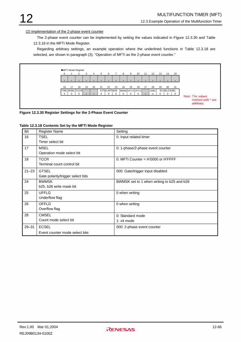
MULTIFUNCTION TIMER (MFT) 12.3 Example Operation of the Multifunction Timer
Rev.1.00 Mar 01,2004 12-66
REJ09B0134-0100Z
12 (2) Implementation of the 2-phase event counter
The 2-phase event counter can be implemented by setting the values indicated in Figure 12.3.30 and Table 12.3.18 in the MFTi Mode Register.
Regarding arbitrary settings, an example operation where the underlined functions in Table 12.3.18 are selected, are shown in paragraph (3), “Operation of MFTi as the 2-phase event counter.”
MFTi Mode Register 0 1 2 3 4 5 6 7 8 9 10 11 12 13 14 15
0 0 0 0 0 0 0 0 0 0 0 0 0 0 0 0
16 17 18 19 20 21 22 23 24 25 26 27 28 29 30 31
TSEL MSEL TCCR GTSEL/MTMOD BWMSK UFFLG OFFLG CMSEL ECSEL/CSSEL 0 0 0 0 0 0 0 0 0 0 0 0 * 0 0 0
Note: The values marked with * are arbitrary.
Figure 12.3.30 Register Settings for the 2-Phase Event Counter
Table 12.3.18 Contents Set by the MFTi Mode Register
Bit Register Name Setting 16 TSEL
Timer select bit 0: Input related timer
17 MSEL Operation mode select bit
0: 1-phase/2-phase event counter
18 TCCR Terminal count control bit
0: MFTi Counter = H’0000 or H’FFFF
21–23 GTSEL Gate polarity/trigger select bits
000: Gate/trigger input disabled
24 BWMSK b25, b26 write mask bit
BWMSK set to 1 when writing to b25 and b26
25 UFFLG Underflow flag
0 when writing
26 OFFLG Overflow flag
0 when writing
28 CMSEL Count mode select bit
0: Standard mode 1: x4 mode
29–31 ECSEL Event counter mode select bits
000: 2-phase event counter

MULTIFUNCTION TIMER (MFT) 12.3 Example Operation of the Multifunction Timer
Rev.1.00 Mar 01,2004 12-67
REJ09B0134-0100Z
12 (3) Operation of MFTi as the 2-phase event counter
Figure 12.3.31 and Figure 12.3.32 show example operation timings of MFTi when acting as the 2-phase event counter that was set in (2).
Shown in Figure 12.3.31 and Figure 12.3.32 are examples for the case when standard mode is selected (CMSEL = 0) and when x4 mode is selected (CMSEL = 1), respectively.
0002 0001 FFFD FFFB0003 0000 FFFFFFFE FFFF 0000 0001 0002
MFTi invocation
MFTi enable bit setto 1
MFTi enable bitcleared to 0
Up count Down count
Event A input
MFTi enablebit
Event B input
MFTi Countervalue
Behavior of theMFTi Counter
"H'0002"
Interrupt requestoutput
(internal signal)
DMA request output(internal signal)
FFFE FFFC
"H'FFFF"
"H'0000"
Count direction (standard mode)
Count direction Input
Up count Down count
Event A input High level
Event B input
Figure 12.3.31 Example Operation Timing of MFTi when Acting as 2-Phase Event Counter (when standard mode is
selected)

MULTIFUNCTION TIMER (MFT) 12.3 Example Operation of the Multifunction Timer
Rev.1.00 Mar 01,2004 12-68
REJ09B0134-0100Z
12
0002 0001 FFFD FFFB0003 0000 FFFFFFFE FFFF 0000 0001 0002
MFTi invocation
MFTi enable bitset to 1
MFTi enable bitcleared to 0
Up count Down count
Event A input
MFTi enable bit
Event B input
MFTi Countervalue
Behavior of theMFTi Counter
"H'0002"
Interrupt requestoutput
(internal signal)DMA request
output(internal signal)
FFFE FFFC
"H'FFFF"
"H'0000"
Count direction (x4 mode)
Count direction Input
Up count Down count
Event A input High level Low level High level Low level
Event B input Low level High level High level Low level
Figure 12.3.32 Example Operation Timing of MFTi when Acting as 2-Phase Event Counter (when x4 mode is
selected)

MULTIFUNCTION TIMER (MFT) 12.4 Example Multifunction Timer Setup Procedure
Rev.1.00 Mar 01,2004 12-69
REJ09B0134-0100Z
12 12.4 Example Multifunction Timer Setup Procedure
The following shows an example multifunction timer setup procedure.
(1) CLK Controller Set up the controller to supply the module operating clock and clock driver clock.
(2) MFTi Mode Register
(3) MFTi Pin Output Status Register
(4) MFTi Compare Reload Register
When using compare match
(5) MFTi Counter and MFTi Reload Register
(6) MFTi Real Port Register
(7) Interrupt Controller and DMA Controller registers
When using interrupts and DMA transfers
(8) Port registers
When using MFTi output pins
(9) MFT Control Register
Enable MFTi operation
Figure 12.4.1 Example Procedure for Setting Up MFT Related Registers
Setu
p pr
oced
ure

MULTIFUNCTION TIMER (MFT) 12.4 Example Multifunction Timer Setup Procedure
Rev.1.00 Mar 01,2004 12-70
REJ09B0134-0100Z
12
This page is blank for reasons of layout.

CHAPTER 13SERIAL I/O (SIO) CHAPTER 13
SERIAL I/O (SIO)

SERIAL I/O (SIO) 13.1 Outline of the Serial I/O
Rev.1.00 Mar 01,2004 13-2
REJ09B0134-0001Z
13 13.1 Outline of the Serial I/O
The OPSP incorporates two-channel serial I/Os (SIOs) which are switchable between CSIO mode (clock-synchronous) and UART mode (clock-asynchronous).
CSIO mode (clock-synchronous)
Communication is performed synchronously by using the same transfer clock on both transmit and receive sides. The transfer data length can be selected from 5–16 bits.
UART mode (clock-asynchronous) Communication can be performed at any transfer rate in any transfer data format that is set. The transfer data
length can be selected from 5–16 bits.
Table 13.1.1outlines the serial I/O. Figure 13.1.1 shows a block diagram of the SIO. Note that the letter ‘i’ in SIOi in this chapter denotes channels 0 and 1.
Table 13.1.1 Outline of the SIO
Outline Item
CSIO mode UART mode
Number of
channels
2 (SIO0–1: Switchable between UART mode and CSIO mode)
Clock Internal clock/external clock Note Internal clock
Transfer mode Transmit half duplex, receive half duplex, transmit/receive full duplex
Data format Transfer data length: 5–16 bits Order of transfer: LSB first or MSB first
Transfer data length: 5–16 bits Order of transfer: LSB first or MSB first Start bit: 1 bit Stop bit: 1 or 2 bits Parity bit: Included (odd, even,
space, mark) or none
Baud rate 254 bps to 8.3333 Mbps (at f(PCLK) = 33 MHz) 31.8 bps to 2083331.3 bps (at f(PCLK) = 33 MHz) Baud rate correction function available
Error detection Overrun Overrun, parity, framing
Interrupt
request
Transmit buffer register empty Transmission completed (transmit shift register empty) Reception completed (receive buffer full) Receive error detected
DMA request Transmit buffer register empty Reception completed (receive buffer full)
Note: The maximum input frequency of external clock is f(PCLK) / 4, where f(PCLK) = frequency of PCLK (peripheral I/O clock). The input signal to the SCLKi pin is sampled with the PCLK (peripheral I/O clock).

SERIAL I/O (SIO) 13.1 Outline of the Serial I/O
Rev.1.00 Mar 01,2004 13-3
REJ09B0134-0001Z
13
Baud Rate Generator
(BRG)
Internal data bus
To the Interrupt Controller
Transmit interrupt request
Receive interrupt request
Transmit DMA request
Receive DMA request
Transmit/Receive Control Circuit
To the DMAC
SIOi Transmit Buffer Register
RXDi
RTSi#
CTSi#
TXDi
CSIO mode when internal clock selected
CSIO mode when external clock selected
CSIO mode
Baud Rate Corrector
1/16
1/(n+1)
PCLK
SCLKi
SIOi Transmit Shift Register
SIOi Receive Buffer Register
SIOi Receive Shift Register
UART mode
LSB/MSB first selected
LSB/MSB first selected
1/2
Figure 13.1.1 Block Diagram of the SIO

SERIAL I/O (SIO) 13.2 Serial I/O Related Registers
Rev.1.00 Mar 01,2004 13-4
REJ09B0134-0001Z
13
13.2 Serial I/O Related Registers The following shows a memory map of serial I/O related registers and describes each register.
SIO Register Mapping
Address b0 +0 address b7 b8 +1 address b15 b16 +2 address b23 b24 +3 address b31
H'00EF D000 SIO0 Control Register (SIO0CR)
H'00EF D004 SIO0 Mode Register 0 (SIO0MOD0)
H'00EF D008 SIO0 Mode Register 1 (SIO0MOD1)
H'00EF D00C SIO0 Status Register (SIO0STS)
H'00EF D010 SIO0 Transfer Processing Control Register (SIO0TRCR)
H'00EF D014 SIO0 Baud Rate Register (SIO0BAUR)
H'00EF D018 SIO0 Baud Rate Correction Register (SIO0RBAUR)
H'00EF D01C SIO0 Transmit Buffer Register
(SIO0TXB)
H'00EF D020 SIO0 Receive Buffer Register
(SIO0RXB)
~ (Use of this area prohibited)
H'00EF D100 SIO1 Control Register (SIO1CR)
H'00EF D104 SIO1 Mode Register 0 (SIO1MOD0)
H'00EF D108 SIO1 Mode Register 1 (SIO1MOD1)
H'00EF D10C SIO1 Status Register (SIO1STS)
H'00EF D110 SIO1 Transfer Processing Control Register (SIO1TRCR)
H'00EF D114 SIO1 Baud Rate Register (SIO1BAUR)
H'00EF D118 SIO1 Baud Rate Correction Register (SIO1RBAUR)
H'00EF D11C SIO1 Transmit Buffer Register
(SIO1TXB)
H'00EF D120 SIO1 Receive Buffer Register
(SIO1RXB)

SERIAL I/O (SIO) 13.2 Serial I/O Related Registers
Rev.1.00 Mar 01,2004 13-5
REJ09B0134-0001Z
13 13.2.1 SIOi Control Registers
SIO0 Control Register (SIO0CR) <Address: H’00EF D000>
SIO1 Control Register (SIO1CR) <Address: H’00EF D100>
b0 1 2 3 4 5 6 7 8 9 10 11 12 13 14 b15
0 0 0 0 0 0 0 0 0 0 0 0 0 0 0 0
b16 17 18 19 20 21 22 23 24 25 26 27 28 29 30 b31
RSCLR TSCLR RXEN TXEN0 0 0 0 0 0 0 0 0 0 0 0 0 0 0 0
* This register can be accessed bytewise (in 8 bits), halfwordwise (in 16 bits) or wordwise (in 32 bits)
<After reset: H’0000 0000>
b Bit Name Function R W
0–21 No functions assigned. Fix these bits to 0. 0 0
22 RSCLR
Receive status initialization bit
0: No operation
1: Initialize the receive status bit
0 Note
23 TSCLR
Transmit status initialization bit
0: No operation
1: Initialize the transmit status bit
0 Note
24–29 No functions assigned. Fix these bits to 0. 0 0
30 RXEN
Receive enable bit
0: Disable reception
1: Enable reception
R W
31 TXEN
Transmit enable bit
0: Disable transmission
1: Enable transmission
R W
Note: This means that writing data “0” has no effect, and that data “1” written to the bit is not retained.
(1) RSCLR (receive status initialization) bit (b22)
This bit initializes the receive status of SIOi. Clearing this bit to 0 has no effect, with the write operation ignored. When this bit is set to 1, the following registers are initialized: Receive status bits in the SIOi Status Register (b22, b24–26, b28, b29) SIOi Receive Shift Register
All other registers are unaffected. Note that even when this bit is set to 1, the value in it is not retained. If this bit is set to 1 while receiving data, the receive operation is forcibly stopped, in which case the received
data cannot be guaranteed
(2) TSCLR (transmit status initialization) bit (b23) This bit initializes the transmit status of SIOi. Clearing this bit to 0 has no effect, with the write operation ignored. When this bit is set to 1, the following registers are initialized: Transmit status bits in the SIOi Status Register (b23, b30, b31) SIOi Transmit Shift Register
Transmit-completed interrupt requests, if any, are cleared at the same time. All other registers are unaffected.
Note that even when this bit is set to 1, the value in it is not retained. If this bit is set to 1 while transmitting data, the transmit operation is forcibly stopped, in which case the
transmitted data cannot be guaranteed

SERIAL I/O (SIO) 13.2 Serial I/O Related Registers
Rev.1.00 Mar 01,2004 13-6
REJ09B0134-0001Z
13 (3) RXEN (receive enable) bit (b30)
This bit enables or disables reception. Clearing this bit to 0 disables reception. However, if this bit is cleared to 0 when receiving data, reception is not
disabled until the receive operation in progress finishes. Setting this bit to 1 enables reception. If any receive error flag Note is set, this bit is cleared to 0, with reception thereby disabled. If the receive enable
bit is set to 1 while this receive error flag remains set, device operation cannot be guaranteed. Note: The SIO module has three receive error flags (b24–b26 in the SIOi Status Register). For details, refer to
Section 13.2.4, “SIOi Status Registers.” (4) TXEN (transmit enable) bit (b31)
This bit enables or disables transmission. Clearing this bit to 0 disables transmission. However, if this bit is cleared to 0 when transmitting data,
transmission is not disabled until the transmit operation in progress finishes. Setting this bit to 1 enables transmission. If the receive overrun flag (SIOi Status Register OERR bit) is set to 1 when operating in CSIO mode, the
receive enable bit is cleared (reception disabled) and this bit is cleared to 0 at the same time, with transmission thereby disabled.

SERIAL I/O (SIO) 13.2 Serial I/O Related Registers
Rev.1.00 Mar 01,2004 13-7
REJ09B0134-0001Z
13 13.2.2 SIOi Mode Register 0
SIO0 Mode Register 0 (SIO0MOD0) <Address: H’00EF D004>
SIO1 Mode Register 0 (SIO1MOD0) <Address: H’00EF D104>
b0 1 2 3 4 5 6 7 8 9 10 11 12 13 14 b15
0 0 0 0 0 0 0 0 0 0 0 0 0 0 0 0
b16 17 18 19 20 21 22 23 24 25 26 27 28 29 30 b31
RTST RTSS CTSS UCS PEN PSEL TSTB RSTB0 0 0 0 0 0 0 0 0 0 0 0 0 0 0 0
* This register can be accessed bytewise (in 8 bits), halfwordwise (in 16 bits) or wordwise (in 32 bits)
<After reset: H’0000 0000>
b Bit Name Function R W
0–22 No functions assigned. Fix these bits to 0. 0 0
23 RTST
RTS timing select bit
0: Continuous RTS timing
1: Single-shot RTS timing
R W
24 RTSS
RTS function select bit
0: Disable RTS function
1: Enable RTS function
R W
25 CTSS
CTS function select bit
0: Disable CTS function
1: Enable CTS function
R W
26 UCS
UART/CSIO function select bit
0: UART mode
1: CSIO mode
R W
27 PEN
Parity enable bit
(UART mode-only bit)
0: Disable parity
1: Enable parity
R W
28–29 PSEL
Parity enable bits
(UART mode-only bits)
00: Even parity
01: Odd parity
10: Space (“0”)
11: Mark (“1”)
R W
30 TSTB
Transmit stop bit length select bit
(UART mode-only bit)
0: One stop bit
1: Two stop bits
R W
31 RSTB
Receive stop bit length select bit
(UART mode-only bit)
0: One stop bit
1: Two stop bits
R W
Note: Make sure that bits in SIOi Mode Register 0 are set while SIO is idle (transmit and receive enable bits both disabled, with no data being transmitted or received).

SERIAL I/O (SIO) 13.2 Serial I/O Related Registers
Rev.1.00 Mar 01,2004 13-8
REJ09B0134-0001Z
13 (1) RTST (RTS timing select) bit (b23)
This bit selects the timing at which the RTSi# pin changes state. The value set in this bit takes effect when the RTS function is enabled (RTSS = 1).
If this bit is cleared to 0, the RTSi# signal is controlled with the continuous receive timing of the RTS# pin. If this bit is set to 1, the RTSi# signal is controlled with the single-shot receive timing of the RTS# pin. For details about the timing at which the RTSi# pin changes state, refer to Section 13.3, “Description of CSIO
Operation,” and Section 13.4, “Description of UART Operation.”
(2) RTSS (RTS function select) bit (b24)
This bit enables or disables the RTS function. Clearing this bit to 0 disables the RTS function, in which case the RTSi# pin always output a high. Setting this bit to 1 enables the RTS function, in which case the RTSi# pin changes state depending on how
the RTS timing select bit (RTST) is set. For details about the timing at which the RTS# pin changes state, refer to Section 13.3, “Description of CSIO
Operation,” and Section 13.4, “Description of UART Operation.”
(3) CTSS (CTS function select) bit (b25)
This bit enables or disables the CTS function. Clearing this bit to 0 disables the CTS function. Setting this bit to 1 enables the CTS function. During UART mode, a low-level signal input to the CTSi# pin is used as one of transmit conditions. During CSIO mode, a low-level signal input to the CTSi# pin is used as one of transmit or receive conditions. For details about transmit and receive conditions, refer to Section 13.3, “Description of CSIO Operation,” and
Section 13.4, “Description of UART Operation.”
(4) UCS (UART/CSIO function select) bit (b26)
This bit selects SIO mode. Clearing this bit to 0 selects UART mode. Setting this bit to 1 selects CSIO mode.
(5) PEN (parity enable) bit (b27)
This bit enables or disables parity. The value set in this bit takes effect when UART mode is selected (UCS = 0).
Clearing this bit to 0 disables parity, so that no parity bits are added. The received data is not checked for parity either.
Setting this bit to 1 enables parity, so that parity bits are added. The received data is checked for parity. For details about the transfer data format, refer to Section 13.4, “Description of UART Operation.”
(6) PSEL (parity select) bits (b28–b29)
These bits select parity from four choices available: even parity, odd parity, space (parity data “0”) or mark (parity data “1”). The value set in these bits takes effect when UART mode is selected and parity is enabled (PEN = 1).
The parity bit selected by these bits is added immediately after the data bits in transmit data. Furthermore, the parity bit selected by these bits is referenced to check for errors in the received data.
For details about the transfer data format, refer to Section 13.4, “Description of UART Operation.”
SERIAL I/O (SIO) 13.2 Serial I/O Related Registers
Rev.1.00 Mar 01,2004 13-9
REJ09B0134-0001Z
13 (7) TSTB (transmit stop bit length select) bit (b30)
This bit selects the length of stop bits that indicate the end of the data (including parity) to be transmitted. The value set in this bit takes effect when UART mode is selected.
If this bit is cleared to 0, one stop bit is transmitted after the last bit of the transmit data. If this bit is set to 1, two stop bits are transmitted after the last bit of the transmit data. For details about the transfer data format, refer to Section 13.4, “Description of UART Operation.”
(8) RSTB (receive stop bit length select) bit (b31)
This bit selects the length of stop bits that indicate the end of the data (including parity) to be received. The value set in this bit takes effect when UART mode is selected.
If this bit is cleared to 0, SIO assumes that one stop bit is to be received after the last bit of the received data as it checks for framing errors.
If this bit is set to 1, SIO assumes that two stop bits are to be received after the last bit of the received data as it checks for framing errors.
For details about the transfer data format, refer to Section 13.4, “Description of UART Operation.”

SERIAL I/O (SIO) 13.2 Serial I/O Related Registers
Rev.1.00 Mar 01,2004 13-10
REJ09B0134-0001Z
13 13.2.3 SIOi Mode Register 1
SIO0 Mode Register 1 (SIO0MOD1) <Address: H’00EF D008>
SIO1 Mode Register 1 (SIO1MOD1) <Address: H’00EF D108>
b0 1 2 3 4 5 6 7 8 9 10 11 12 13 14 b15
0 0 0 0 0 0 0 0 0 0 0 0 0 0 0 0
b16 17 18 19 20 21 22 23 24 25 26 27 28 29 30 b31
CHLS CMSELTXSEL LMFS CKSEL0 0 0 0 0 0 0 0 0 0 0 0 0 0 0 0
* This register can be accessed bytewise (in 8 bits), halfwordwise (in 16 bits) or wordwise (in 32 bits)
<After reset: H’0000 0000>
b Bit Name Function R W
0–19 No functions assigned. Fix these bits to 0. 0 0
20–23 CHLS
Character length select bits
0000: 16-bit character
0001: Setting prohibited
0010: Setting prohibited
0011: Setting prohibited
0100: Setting prohibited
0101: 5-bit character
0110: 6-bit character
0111: 7-bit character
1000: 8-bit character
1001: 9-bit character
1010: 10-bit character
1011: 11-bit character
1100: 12-bit character
1101: 13-bit character
1110: 14-bit character
1111: 15-bit character
R W
24 No functions assigned. Fix these bits to 0. 0 0
25 CMSEL
SCLKi pin output mode select bit
(used only when CSIO mode and internal
clock output selected)
0: CMOS output
1: N-ch open-drain
R W
26 TXSEL
TXDi pin output mode select bit
0: CMOS output
1: N-ch open-drain
R W
27 LMFS
LSB/MSB first select bit
0: LSB first
1: MSB first
R W
28–30 No functions assigned. Fix these bits to 0. 0 0
31 CKSEL
Internal/external clock select bit
0: Internal clock
1: External clock
R W
Note: Make sure that bits in SIOi Mode Register 0 are set while SIO is idle (transmit and receive enable bits both disabled, with no data being transmitted or received).

SERIAL I/O (SIO) 13.2 Serial I/O Related Registers
Rev.1.00 Mar 01,2004 13-11
REJ09B0134-0001Z
13 (1) CHLS (character length select) bits (b20–b23)
These bits select the character length of the data to be transmitted/received. The data bits that are not used as determined by the transfer character length are set to 0s. Figure 13.2.1 shows an example transmit/receive data when the character length is chosen to be 7 bits.
Example transmit/receive data when the character length is 7 bits
<When transmitting>
Data in the SIOi Transmit Buffer Register * * * * * * * * * D9 D10 D11 D12 D13 D14 D15
Transmit data (LSB first) D15→D14→D13→D12→D11→D10→D9
1st bit of the transmit data
7th bit of the transmit data
The data marked with * are not output.
Receive data (LSB first) D15→D14→D13→D12→D11→D10→D9
1st bit of the receive data
7th bit of the receive data
<When receiving>
Data in the SIOi Receive Buffer Register 0 0 0 0 0 0 0 0 0 D9 D10 D11 D12 D13 D14 D15
b16 b31
b16 b31
Figure 13.2.1 Example Transmit/Receive Data for 7-Bit Character
(2) CMSEL (SCLKi pin output mode select) bit (b25)
This bit selects SCLKi pin output mode between CMOS output or N-ch open-drain. The value set in this bit takes effect when internal clock is selected (CKSEL = 0) during CSIO mode (CSIOi Mode Register 0 UCS bit = 1).
If this bit is cleared to 0, the SCLKi pin operates as CMOS output. If this bit is set to 1, the SCLKi pin operates as N-ch open-drain output.
Note: If open-drain output mode is selected, an external resistor may be needed to pull the SCLKi pin high.

SERIAL I/O (SIO) 13.2 Serial I/O Related Registers
Rev.1.00 Mar 01,2004 13-12
REJ09B0134-0001Z
13 (3) TXSEL (TXDi pin output mode select) bit (b26)
This bit selects TXDi pin output mode between CMOS output or N-ch open-drain. The value set in this bit takes effect when internal clock is selected (CKSEL = 0).
If this bit is cleared to 0, the TXDi pin operates as CMOS output. If this bit is set to 1, the TXDi pin operates as N-ch open-drain output. If the TXDi pin is set for N-ch open-drain output during CSIO mode (SIOi Mode Register 0 UCS bit = 1), the
TXDi pin is placed in the high-impedance state a half transfer clock period after the last rise of the transfer clock. If external clock is selected, the TXDi pin operates as CMOS output no matter how the TXDi pin output mode select bit is set.
If the TXDi pin is set for N-ch open-drain output during UART mode, the TXDi pin outputs a low at the start bit and goes to a high-impedance state at the stop bit.
Figure 13.2.2 shows examples of TXDi signal output.
Note: If open-drain output mode is selected, an external resistor may be needed to pull the SCLKi pin high.
During CSIO mode where TXD signal is set for CMOS output, with transfer data sampled at rising edges
SCLKi (input or output)
TXDi D15 D14 D13 D12 D11 D10 D9 D8
During CSIO mode where TXD signal is set for N-ch open-drain output (only when internal clock is selected)
SCLKi (input or output)
TXDi D15 D14 D13 D12 D11 D10 D9 D8
Half transfer clock period
Hi-Z state Hi-Z state
During UART mode where TXDi signal is set for CMOS output
Transfer clock (internal signal)
TXDi D15 D14 D13 D12 D11 D10 D9 D8 ST SP
During UART mode where TXDi signal is set for N-ch open-drain output
Transfer clock (internal signal)
TXDi D15 D14 D13 D12 D11 D10 D9 D8 ST SP
Figure 13.2.2 Example of TXDi Signal Output

SERIAL I/O (SIO) 13.2 Serial I/O Related Registers
Rev.1.00 Mar 01,2004 13-13
REJ09B0134-0001Z
13 (4) LMFS (LSB/MSB first select) bit (b27)
This bit selects the order in which data is transferred (LSB first or MSB first). If this bit is cleared to 0, data is transferred beginning with the LSB (bit 31 in the SIOi Transmit Buffer Register).
For example, if the transfer data length is chosen to be 8 bits by the character length bits (CHLS), data is transferred in order of bit 31, bit 30, ..., bit 25 and bit 24 of the SIOi Transmit Buffer Register.
If this bit is set to 1, data is transferred beginning with the MSB (the bit close to bit 16 in the SIOi Transmit Buffer Register). For example, if the transfer data length is chosen to be 10 bits by the character length select bits (CHLS), data is transferred in order of bit 22, bit 23, ..., bit 30 and bit 31 of the SIOi Transmit Buffer Register.
Thus, if MSB first is selected, the bit number from which a transfer starts varies depending on the number of transfer bits selected by the character length select bits, and the last data bit transferred is always bit 31 of the SIOi Transmit Buffer Register.
Figure 13.2.3 schematically shows the order in which data bits are transferred.
When transmitting 16-bit data MSB first
Data in the SIOi Transmit Buffer
Register D0 D1 D2 D3 D4 D5 D6 D7 D8 D9 D10 D11 D12 D13 D14 D15
b16 b31 b23 b24
Data in the SIOi Transmit Shift
Register D15 D14 D13 D12 D11 D10 D9 D8 D7 D6 D5 D4 D3 D2 D1 D0
Load
16th bit of transmit data
1st bit of transmit data
When transmitting 8-bit data LSB first
Data in the SIOi Transmit Buffer
Register * * * * * * * * D8 D9 D10 D11 D12 D13 D14 D15
b16 b31 b23 b24
Data in the SIOi Transmit Shift
Register * * * * * * * * D8 D9 D10 D11 D12 D13 D14 D15
Load
8th bit of transmit data
1st bit of transmit data
When receiving 16-bit data MSB first
Data in the SIOi Receive Shift
Register D0 D1 D2 D3 D4 D5 D6 D7 D8 D9 D10 D11 D12 D13 D14 D15
b16 b31 b23 b24Data in the SIOi Receive Buffer
Register D0 D1 D2 D3 D4 D5 D6 D7 D8 D9 D10 D11 D12 D13 D14 D15
1st bit of received data
16th bit of received data
When receiving 8-bit data LSB first
Data in the SIOi Receive Shift
Register * * * * * * * * D15 D14 D13 D12 D11 D10 D9 D8
b16 b31 b23 b24Data in the SIOi Receive Buffer
Register 0 0 0 0 0 0 0 0 D8 D9 D10 D11 D12 D13 D14 D15
1st bit of received data
8th bit of received data
Load
Note: The data bits marked with * arenot transferred.
Note: The data bits marked with * arenot loaded. Load
Transmission
Transmission
Reception
Reception
Figure 13.2.3 Image Depicting the Order Data Bits are Transferred

SERIAL I/O (SIO) 13.2 Serial I/O Related Registers
Rev.1.00 Mar 01,2004 13-14
REJ09B0134-0001Z
13 (5) CKSEL (internal/external clock select) bit (b31)
This bit selects to use the internal clock (PCLK) or the external clock supplied to the SCLKi pin as the transfer clock.
If this bit is cleared to 0, the internal clock (PCLK) is used. If this bit is set to 1, the external clock supplied to the SCLKi pin is used. The following shows how the selected clock will be used.
<During UART mode>
When internal clock is selected PCLK is input to the Baud Rate Generator.
When external clock is selected No external clocks can be used.
<During CSIO mode>
When internal clock is selected PCLK is input to the Baud Rate Generator. The transfer clock is output from the SCLKi pin, to control transmission/reception.
When external clock is selected The transfer clock supplied from the SCLKi pin is used to control transmission/reception. The Baud Rate
Generator is unused. The maximum frequency of the input clock to the SCLKi pin is f(PCLK) / 4. The input signal to the SCLKi pin is sampled using the internal clock (PCLK).

SERIAL I/O (SIO) 13.2 Serial I/O Related Registers
Rev.1.00 Mar 01,2004 13-15
REJ09B0134-0001Z
13 13.2.4 SIOi Status Registers
SIO0 Status Register (SIO0STS) <Address: H’00EF D00C>
SIO1 Status Register (SIO1STS) <Address: H’00EF D10C>
b0 1 2 3 4 5 6 7 8 9 10 11 12 13 14 b15
0 0 0 0 0 0 0 0 0 0 0 0 0 0 0 0
b16 17 18 19 20 21 22 23 24 25 26 27 28 29 30 b31
RXSC TXSC FERR PERR OERR RXSF RXCP TXCP TEMP0 0 0 0 0 0 0 0 0 0 0 0 0 0 1 1
* This register can be accessed bytewise (in 8 bits), halfwordwise (in 16 bits) or wordwise (in 32 bits)
<After reset: H’0000 0003>
b Bit Name Function R W
0–21 No functions are assigned. When read, these bits are 0. 0 N
22 RXSC
Receive shift register status flag
0: Not receiving data
1: Receiving data now
R N
23 TXSC
Transmit shift register status flag
0: Not transmitting data
1: Transmitting data now
R N
24 FERR
Receive framing error flag (UART mode only)
0: No receive framing error
1: Receive framing error detected
R N
25 PERR
Receive parity error flag (UART mode only)
0: No receive parity error
1: Receive parity error detected
R N
26 OERR
Receive overrun error flag
0: No receive overrun error
1: Receive overrun error detected
R N
27 No functions are assigned. 0 N
28 RXSF
Receive shift register full flag
0: No data in SIOi Receive Shift Register
1: Data present in SIOi Receive Shift Register
R N
29 RXCP
Reception-completed flag
(receive buffer register full)
0: No data in SIOi Receive Buffer Register
1: Data present in SIOi Receive Buffer Register
R N
30 TXCP
Transmission-completed flag
(transmit shift register empty)
0: Data present in SIOi Transmit Shift Register
1: No data in SIOi Transmit Shift Register
R N
31 TEMP
Transmit buffer empty flag
0: Data present in SIOi Transmit Buffer Register
1: No data in SIOi Transmit Buffer Register
R N
Note: This register is a read-only register.

SERIAL I/O (SIO) 13.2 Serial I/O Related Registers
Rev.1.00 Mar 01,2004 13-16
REJ09B0134-0001Z
13 (1) RXSC (receive shift register status flag) bit (b22)
This bit allows to inspect the status of the SIOi Receive Shift Register. Conditions under which this bit is set and cleared differ between UART and CSIO modes, as described below.
<During UART mode (SIOi Mode Register 0 UCS bit = 0)>
Set (= 1) condition This bit is set to 1 when RXDi is sampled low again after the start bit is detected (falling edge of the input
signal to the RXDi pin). Clear (= 0) condition
This bit is cleared to 0 when SIO has finished receiving the last stop bit.
<During CSIO mode (SIOi Mode Register 0 UCS bit = 1)>
Set (= 1) condition This bit is set to 1 by a falling edge of the transfer clock at the first bit of data to be received.
Clear (= 0) condition This bit is cleared to 0 by a rising edge of the transfer clock at the last bit to be received.

SERIAL I/O (SIO) 13.2 Serial I/O Related Registers
Rev.1.00 Mar 01,2004 13-17
REJ09B0134-0001Z
13 (2) TXSC (transmit shift register status flag) bit (b23)
This bit allows to inspect the status of the SIOi Transmit Shift Register. Conditions under which this bit is set and cleared differ between UART and CSIO modes, as described below.
<During UART mode (SIOi Mode Register 0 UCS bit = 0)>
Set (= 1) condition This bit is set to 1 upon detection of the start bit (falling edge of the input signal to the TXDi pin).
Clear (= 0) condition This bit is cleared to 0 by a falling edge of the transfer clock at the last stop bit to be transmitted.
<During CSIO mode (SIOi Mode Register 0 UCS bit = 1)>
Set (= 1) condition This bit is set to 1 by a falling edge of the transfer clock at the first bit of data to be transmitted.
Clear (= 0) condition This bit is cleared to 0 by a rising edge of the transfer clock at the last bit to be transmitted.
Figure 13.2.4 shows example timings of shift register status flags.
Example timing of shift register status flags during UART mode (when baud rate setting bits = H’0001 (divide-by-2) and baud rate correction bits = H’4 (correction value 8))
Count source to BRG
BRG output clock
1 2
1 2 3 4 5 6 7 8
1 2 3 4
10 11 12 13 14 15 16
5 6 7 8
9
Start bit
RXDi ST
Start bit sampling points
TXDi ST
1 2 3 4 5 6 7 8
1 2 3 4
10 11 9
Stop bit 1 2
Receive shift register status flag
Transmit shift register status flag
SP
SP
Stop bit sampling points
If two stop bits are included, the flag is cleared at the last stop bit sampling point.
Example timing of shift register status flags during CSIO mode (when transfer data consisting of 8 bits)
Transfer clock
RXDi、TXDi
Receive shift register status flag
Transmit shift register status flag
D15 D14 D13 D12 D11 D10 D9 D8
Figure 13.2.4 Example Timings of Shift Register Status Flags

SERIAL I/O (SIO) 13.2 Serial I/O Related Registers
Rev.1.00 Mar 01,2004 13-18
REJ09B0134-0001Z
13 (3) FERR (receive framing error flag) bit (b24)
This bit allows to inspect the status of receive framing errors in the received data. This bit is effective when UART mode is selected. The following describes conditions under which this bit is set and cleared.
Set (= 1) condition
If the number of stop bits in the received data does not match the one that was selected by the receive stop bit length select bit (SIOi Mode Register 0 RSTB bit), a framing error is detected upon receiving the last stop bit and this bit is set to 1. In this case, the receive enable bit is cleared to 0, with reception thereby disabled.
For the data which has had this bit set to 1, the reception-completed flag (RXCP) is not set to 1. Note also
that if the receive enable bit is set to 1 while this bit remains set, device operation cannot be guaranteed.
Clear (= 0) condition
When the SIOi Status Register is read When the receive status initialization bit (SIOi Control Register RSCLR bit) is set to 1
Note that this bit is not cleared by a read of the SIOi Receive Buffer Register.
(4) PERR (receive parity error flag) bit (b25)
This bit allows to inspect the status of receive parity errors in the received data. This bit takes effect when UART mode is selected (SIOi Mode Register 0 UCS bit = 0) and parity is enabled (SIOi Mode Register 0 PEN bit = 1). The following describes conditions under which this bit is set and cleared.
Set (= 1) condition
If the parity attribute of the received data does not match the one that was set by the parity select bits (SIOi Mode Register 0 PSEL bits), a parity error is detected upon receiving the last stop bit and this bit is set to 1. In this case, the receive enable bit is cleared to 0, with reception thereby disabled.
For the data which has had this bit set to 1, the reception-completed flag is not set to 1. Note also that if
the receive enable bit is set to 1 while this bit remains set, device operation cannot be guaranteed.
Clear (= 0) condition
When the SIOi Status Register is read When the receive status initialization bit (SIOi Control Register RSCLR bit) is set to 1
Note that this bit is not cleared by a read of the SIOi Receive Buffer Register.

SERIAL I/O (SIO) 13.2 Serial I/O Related Registers
Rev.1.00 Mar 01,2004 13-19
REJ09B0134-0001Z
13 (5) OERR (receive overrun error flag) bit (b26)
This bit allows to check for receive overrun errors. The following describes conditions under which this bit is set and cleared.
Set (= 1) condition
If it is recognized Note that SIO has started receiving the next receive data while the received data exists in the SIOi Receive Buffer Register and Receive Shift Register, an overrun error is detected and this bit is set to 1.
In this case, the data existing in the SIOi Receive Buffer Register and Receive Shift Register is not
overwritten. Therefore, the data in overrun error is not received at all. The receive enable bit is cleared to 0 upon detecting an overrun error, with reception thereby disabled,
and if the error occurred during CSIO mode (SIOi Mode Register 0 UCS bit = 1) the transmit enable bit (SIOi Control Register TXEN bit) also is cleared to 0, with transmission thereby disabled. If the receive enable or transmit enable bit is set to 1 while this bit remains set, device operation cannot be guaranteed.
Note: During UART mode, SIO is recognized to have started receiving data when RXDi is sampled low
again after detection of the start bit. During CSIO mode, SIO is recognized to have started receiving data when a falling edge of the transfer clock is detected at the first bit of data.
Clear (= 0) condition
When the SIOi Status Register is read When the receive status initialization bit (SIOi Control Register RSCLR bit) is set to 1
(6) RXSF (receive shift register full flag) bit (b28)
This bit allows to check for the presence of data in the SIOi Receive Shift Register. The following describes conditions under which this bit is set and cleared.
Set (= 1) condition
This bit is set to 1 when the next data not in error has been received Note while data is present in the SIOi Receive Buffer Register (RXCP = 1) and no data exists in the SIOi Receive Shift Register.
Note: During UART mode, this is when SIO has finished receiving the last stop bit. During CSIO mode, this
is when SIO has finished receiving the last bit of data.
Clear (= 0) condition When the SIOi Receive Buffer Register is read When the receive status initialization bit (SIOi Control Register RSCLR bit) is set to 1 Note that this bit is not cleared by a read of the SIOi Status Register.
(7) RXCP (reception completed (receive buffer register full) flag) bit (b29)
This bit allows to check for the presence of data in the SIOi Receive Buffer Register. The following describes conditions under which this bit is set and cleared.
Set (= 1) condition
This bit is set to 1 when the normally received data has been transferred from the SIOi Receive Shift Register to the SIOi Receive Buffer Register.

SERIAL I/O (SIO) 13.2 Serial I/O Related Registers
Rev.1.00 Mar 01,2004 13-20
REJ09B0134-0001Z
13
Clear (= 0) condition When the SIOi Receive Buffer Register is read while no data exists in the SIOi Receive Shift Register
(RXSF = 0) When the receive status initialization bit (SIOi Control Register RSCLR bit) is set to 1 Note that this bit is not cleared by a read of the SIOi Status Register.
Figure 13.2.5 and Figure 13.2.6 show example timings at which the receive status flags are set and cleared during
UART mode. Figure 13.2.7 shows example timings at which the receive status flags are set and cleared during CSIO mode.
For other than overrun error
Receive enable bit
DATA1
RXDi
Reception-completed flag
Set to 1
SIOi Receive Shift Register DATA2 DATA3 DATA4
SIOi Receive Buffer Register
Receive shift register
full flag
DATA1 DATA2
SIOi Receive Buffer Register read
Receive error flags other than overrun
DATA3 DATA4
SIOi Receive Buffer Register read
Reception-completed processing request output
(internal signal)
Processing request for DATA1
SIOi StatusRegister read
Interrupt request output (receive error)
Processing request for DATA3
(1) (2) (3) (4) (5) (6) (7) (8)
Set to 1
Cleared to 0 by detection of areceive error
Cleared to 0 by detection of a receive error
STSP
ST SP SP
ST STSP
DATA1 DATA2 (received in error) DATA3 DATA4 (received in error)
Not set whenreceived in error
SIOi StatusRegister read
Not set when received in error
(2) Read the SIOi Receive Buffer Register
SIOi Receive Shift Register RXSF
DATA1
SIOi Receive Buffer Register
DATA1
FERRPERRRXCP
0
0 0
(5) Finished receiving data normally
SIOi Receive Shift Register RXSF
DATA3
SIOi Receive Buffer Register
DATA3
FERR PERR RXCP
0
1 0
(6) Finished receiving data in error
SIOi Receive Shift Register RXSF
DATA3
SIOi Receive Buffer Register
DATA4(error)
FERRPERRRXCP
0
1 1
(3) Finished receiving data in error
SIOi Receive Shift Register RXSF
DATA2(error)
SIOi Receive Buffer Register
DATA2(error)
FERRPERRRXCP
0
0 1
(4) Read the SIOi Status Register
SIOi Receive Shift Register RXSF
DATA2(error)
SIOi Receive Buffer Register
DATA2(error)
FERR PERR RXCP
0
0 0
(7) Read the SIOi Receive Buffer Register
SIOi Receive Shift Register RXSF
DATA4(error)
SIOi Receive Buffer Register
DATA4(error)
FERRPERRRXCP
0
0 1
(8) Read the SIOi Status Register
SIOi Receive Shift Register RXSF
DATA4(error)
SIOi Receive Buffer Register
DATA4(error)
FERR PERR RXCP
0
0 0
Note: The data in are not overwritten. The data in are overwritten.
(1) Finished receiving data normally
SIOi Receive Shift Register RXSF
DATA1
SIOi Receive Buffer Register
DATA1
FERR PERR RXCP
0
1 0
Figure 13.2.5 Example of Receive Status Flag Set/Clear Timing during UART Mode 1

SERIAL I/O (SIO) 13.2 Serial I/O Related Registers
Rev.1.00 Mar 01,2004 13-21
REJ09B0134-0001Z
13
For overrun error
Receive enable bit
DATA1
RXDi
Reception completed flag
Set to 1
SIOi Receive Shift Register DATA2 DATA3
SIOi Receive Buffer Register
Receive shift register full flag
DATA1 DATA2
SIOi Receive Buffer Register read
Receive overrun error flag
DATA3
SIOi Receive Buffer Register read
Reception-completed processing request output
(internal signal)
Processing request for DATA1
Interrupt request output (receive error)
Processing request for DATA3
(1) (2) (3) (4) (5) (6) (7) (8)
Cleared to 0 by detection of an overrun error
STSP
ST SP SP
ST STSP
DATA1 DATA2 DATA3 DATA4
SIOi Status Register read
Processing request for DATA2
(1) Finished receiving data normally
SIOi Receive Shift Register RXSF
DATA1
SIOi Receive Buffer Register
DATA1
OERR RXCP
0
1 0
(2) Finished receiving data normally
SIOi Receive Shift Register RXSF
DATA1
SIOi Receive Buffer Register
DATA2
OERRRXCP
1
1 0
(5) Detected the next start bit
SIOi Receive Shift Register RXSF
DATA2
SIOi Receive Buffer Register
DATA3
OERR RXCP
1
1 1
(6) Read the SIOi Receive Buffer Register
SIOi Receive Shift Register RXSF
DATA3
SIOi Receive Buffer Register
DATA3
OERRRXCP
0
1 1
(3) Read the SIOi Receive Buffer Register
SIOi Receive Shift Register RXSF
DATA2
SIOi Receive Buffer Register
DATA2
OERRRXCP
0
1 0
(4) Finished receiving data normally
SIOi Receive Shift Register RXSF
DATA2
SIOi Receive Buffer Register
DATA3
OERR RXCP
1
1 0
(7) Read the SIOi Receive Buffer Register
SIOi Receive Shift Register RXSF
DATA3
SIOi Receive Buffer Register
DATA3
OERRRXCP
0
0 1
(8) Read the SIOi Status Register
SIOi Receive Shift Register RXSF
DATA3
SIOi Receive Buffer Register
DATA3
OERR RXCP
0
0 0
Note: The data in are not overwritten. The data in are overwritten.
Figure 13.2.6 Example of Receive Status Flag Set/Clear Timing during UART Mode 2

SERIAL I/O (SIO) 13.2 Serial I/O Related Registers
Rev.1.00 Mar 01,2004 13-22
REJ09B0134-0001Z
13
Receive enable bit
DATA1
RXDi
Reception completed flag
Set to 1
SIOi Receive Shift Register DATA2 DATA3
SIOi Receive Buffer Register
Receive shift register full flag
DATA1 DATA2
SIOi Receive BufferRegister read
Receive overrun error flag
DATA3
SIOi Receive Buffer Register read
Reception-completed processing request output
(internal signal)
Interrupt request output (receive error)
Processing request for DATA1 Processing request for DATA3
(1) (2) (3) (4) (5) (6) (7) (8)
Cleared to 0 by detectionof an overrun error
SCLKi (input)
DATA1 DATA2 DATA3 DATA4
SIOi StatusRegister read
Processing request for DATA2
(1) Finished receiving data normally
SIOi Receive Shift Register RXSF
DATA1
SIOi Receive Buffer Register
DATA1
OERR RXCP
0
1 0
(2) Read the SIOi Receive Buffer Register
SIOi Receive Shift Register RXSF
DATA1
SIOi Receive Buffer Register
DATA1
OERRRXCP
0
0 0
(5) Detected next fall of the transfer clock
SIOi Receive Shift Register RXSF
DATA2
SIOi Receive Buffer Register
DATA3
OERR RXCP
1
1 1
(6) Read the SIOi Receive Buffer Register
SIOi Receive Shift Register RXSF
DATA3
SIOi Receive Buffer Register
DATA3
OERRRXCP
0
1 1
(3) Finished receiving data normally
SIOi Receive Shift Register RXSF
DATA2
SIOi Receive Buffer Register
DATA2
OERRRXCP
0
1 0
(4) Finished receiving data normally
SIOi Receive Shift Register RXSF
DATA2
SIOi Receive Buffer Register
DATA3
OERR RXCP
1
1 0
(7) Read the SIOi Receive Buffer Register
SIOi Receive Shift Register RXSF
DATA3
SIOi Receive Buffer Register
DATA3
OERRRXCP
0
0 1
(8) Read the SIOi Status Register
SIOi Receive Shift Register RXSF
DATA3
SIOi Receive Buffer Register
DATA3
OERR RXCP
0
0 0
Note: The data in are not overwritten. The data in are overwritten.
Figure 13.2.7 Example of Receive Status Flag Set/Clear Timing during CSIO Mode 3

SERIAL I/O (SIO) 13.2 Serial I/O Related Registers
Rev.1.00 Mar 01,2004 13-23
REJ09B0134-0001Z
13 (8) TXCP (transmission completed (transmit shift register empty) flag) bit (b30)
This bit allows to check for the presence of data in the SIOi Transmit Shift Register. If this bit is cleared to 0, it means that data exists in the SIOi Transmit Shift Register which has not all been
transmitted yet. In this case, if transmission is disabled (SIOi Control Register TXEN bit = 1) before a transmit start condition Note is detected, the remaining data will not be transmitted.
If this bit is set to 1, it means that no data exists in the SIOi Transmit Shift Register. Note: For details about transmit start conditions, refer to Section 13.2.9, “SIOi Receive Buffer Registers.”
The following describes conditions under which this bit is set and cleared.
Set (= 1) condition
If one of the following conditions is met when SIO has finished transmitting the data present in the SIOi Transmit Shift Register Note, no transmit data is transferred from the SIOi Transmit Buffer Register to the SIOi Transmit Shift Register and the SIOi Transmit Shift Register remains empty, in which case this bit is set to 1. ( No data exists in the SIOi Transmit Buffer Register (TEMP = 1) ( Transmit enable bit (SIOi Control Register TXEN bit) = 0 ( The input signal to the CTSi# pin remains high while CTS function is selected (SIOi Mode Register 0
CTSS bit = 1) This bit is also set to 1 when the transmit status initialization bit (SIOi Control Register TSCLR bit) is set to
1. Note: During UART mode (SIOi Mode Register 0 UCS bit = 0), the timing at which this bit is set to 1 is when
SIO has finished transmitting the last stop bit. During CSIO mode, the timing at which this bit is set to 1 is when SIO has finished transmitting the last bit of data.
( Clear (= 0) condition
This bit is cleared to 0 when transmit data has been transferred from SIOi Transmit Buffer Register to the SIOi Transmit Shift Register.
(9) TEMP (transmit buffer empty flag) bit (b31)
This bit allows to check to see if any data exists in the SIOi Transmit Buffer Register that has not been transferred to the SIOi Transmit Shift Register yet.
If this bit is cleared to 0, it means that data exists in the SIOi Transmit Buffer Register that has not been transferred to the SIOi Transmit Shift Register yet.
If this bit is set to 1, it means that no data exists in the SIOi Transmit Buffer Register. The following describes conditions under which this bit is set and cleared.
( Set (= 1) condition This bit is set to 1 when transmit data has been transferred Note from the SIOi Transmit Buffer Register to
the SIOi Transmit Shift Register. Note: For conditions under which transmit data is transferred from the SIOi Transmit Buffer Register to the
SIOi Transmit Shift Register, refer to Section 13.2.8, “SIO0 Transmit Buffer Register (SIO0TXB).”
This bit is also set to 1 when the transmit status initialization bit (SIOi Control Register TSCLR bit) is set to
1.
Clear (= 0) condition This bit is cleared to 0 by a write to the SIOi Transmit Buffer Register.

SERIAL I/O (SIO) 13.2 Serial I/O Related Registers
Rev.1.00 Mar 01,2004 13-24
REJ09B0134-0001Z
13 Figure 13.2.8 shows example timings at which the transmit status flags are set and cleared.
Transmit enable bit
TXDi
Transmission-completed interrupt request output
(internal signal)
Set to 1
Transmit buffer empty flag
Transmission completed flag
Transmit buffer empty processing request output
(internal signal)
Transmit interrupt enable bit cleared
Transmit buffer empty flag
Not set because condition for data transfer to SIOi Transmit Shift Register is met
Transmission-completed interrupt request output
(internal signal)
Transmit buffer empty processing request output
(internal signal)
Transmission completed flag
Cleared to 0
SIOi Transmit Buffer Register
DATA1 DATA2 DATA3 DATA4
Not generated because next transmitdata already written to register
Transmit enable bit
TXDi
Set to 1
SCLKi
DATA1 DATA2 DATA3 DATA4
SIOi Transmit Buffer Register DATA1 DATA2 DATA3 DATA4
Cleared to 0 Set to 1
Transmit data written to register Transmit data written to register Transmit data written to register
DATA1 DATA2 DATA3 DATA4
Transmit data written to register Transmit data written to register Transmit data written to register
ST
SP
ST
SP SP
ST ST
SP
During UART mode
During CSIO mode
Set to 1
Transmit interrupt enable bit cleared
Not set because condition for data transfer to SIOi Transmit Shift Register is met
Not generated because next transmit data already written to register
Figure 13.2.8 Example of Transmit Status Flag Set/Clear Timing

SERIAL I/O (SIO) 13.2 Serial I/O Related Registers
Rev.1.00 Mar 01,2004 13-25
REJ09B0134-0001Z
13 13.2.5 SIOi Transfer Processing Control Registers
SIO0 Transfer Processing Control Register (SIO0TRCR) <Address: H’00EF D010>
SIO1 Transfer Processing Control Register (SIO1TRCR) <Address: H’00EF D110>
b0 1 2 3 4 5 6 7 8 9 10 11 12 13 14 b15
0 0 0 0 0 0 0 0 0 0 0 0 0 0 0 0
b16 17 18 19 20 21 22 23 24 25 26 27 28 29 30 b31
REISEL RXCSELTXCSEL REIE RXCEN TXIEN TEMPIE0 0 0 0 0 0 0 0 0 0 0 0 0 0 0 0
* This register can be accessed bytewise (in 8 bits), halfwordwise (in 16 bits) or wordwise (in 32 bits)
<After reset: H’0000 0000>
b Bit Name Function R W
0–24 No functions assigned. Fix these bits to 0. 0 0
25 REISEL
Receive error interrupt condition select bit
0: Generate interrupt when receive error flag is set
1: Generate interrupt when receive error is detected
R W
26 RXCSEL
Reception-completed processing select bit
0: Generate interrupt request
1: Generate DMA request
R W
27 TXCSEL
Transmit buffer empty processing select bit
0: Generate interrupt request
1: Generate DMA request
R W
28 REIE
Receive error interrupt enable bit
0: Disable receive error interrupt
1: Enable receive error interrupt
R W
29 RXCEN
Reception-completed processing enable bit
0: Disable reception-completed processing
1: Enable reception-completed processing
R W
30 TXIEN
Transmission-completed interrupt enable bit
0: Disable transmission-completed interrupt
1: Enable transmission-completed interrupt
R W
31 TEMPIE
Transmit buffer empty processing enable bit
0: Disable transmit butter empty processing
1: Enable transmit butter empty processing
R W
Note: Make sure that bits in the SIOi Transfer Processing Control Register are set while SIO is idle (transmit and receive enable bits both disabled, with no data being transmitted or received).
The SIOi Transfer Processing Control Register can only be rewritten to change settings when there are no interrupt
requests to the ICU (Interrupt Controller) or DMA requests to the DMAC (DMA Controller).
Note: Interrupt requests to the ICU and DMA requests to the DMAC from this SIO are output as an “active-high”
level-sensitive signal.

SERIAL I/O (SIO) 13.2 Serial I/O Related Registers
Rev.1.00 Mar 01,2004 13-26
REJ09B0134-0001Z
13 (1) REISEL (receive error interrupt condition select) bit (b25)
This bit selects the condition under which to generate a receive error interrupt request, i.e., when the receive error flag is set or when a receive error is detected Note. The value set in this bit takes effect only when receive error interrupts are enabled (REIE = 1).
If this bit is cleared to 0, an interrupt request to the ICU (Interrupt Controller) is generated when any receive error flag (SIOi Status Register FERR, PERR or OERR bit) is set.
In this case, although reception for the subsequent data is automatically disabled (SIOi Control Register RXEN = 0) upon detection of a receive error, if unprocessed data remains in the SIOi Receive Buffer Register, no interrupt requests are generated until the unprocessed data is read out.
If this bit is set to 1, an interrupt request to the ICU immediately when any receive error is detected, regardless of the receive error flag status.
In this case, if unprocessed data remains in the SIOi Receive Buffer Register, the receive error flag is not set, so that if it is necessary to identify the receive error, read the SIOi Status Register after reading the unprocessed data out of the SIOi Receive Buffer Register.
Note: If unprocessed data remains in the SIOi Receive Buffer Register when a receive error is detected, the
receive error flag is not set until after the unprocessed data is read out of the register. In this case, there is some time lag before the receive error flag is set after the error is detected.
(2) RXCSEL (reception-completed processing select) bit (b26)
This bit selects the destination to which a reception-completed processing request will be sent. This bit is effective only when reception-completed processing is enabled (RXCEN = 1). If this bit is cleared to 0, an interrupt request to the ICU (Interrupt Controller) is generated when reception has
finished (SIOi Status Register RXCP bit = 1). In this case, the interrupt request is kept active while the reception completed flag (RXCP) in the SIOi Status Register remains set.
If this bit is set to 1, a DMA request to the DMAC (DMA Controller) is generated when reception has finished. In this case, the DMA request is generated all the time the reception completed flag (RXCP) in the SIOi Status Register remains set.
(3) TXCSEL (transmit buffer empty processing select) bit (b27)
This bit selects the destination to which a transmit buffer empty processing request will be sent. This bit is effective only when transmit buffer empty processing is enabled (TEMPIE = 1). If this bit is cleared to 0, an interrupt request to the ICU is generated all the time the transmit buffer remains
empty (SIOi Status Register TEMP bit = 1) and transmission remains enabled (SIOi Control Register transmit enable bit = 1).
If this bit is set to 1, a DMA request to the DMAC is generated all the time the transmit buffer remains empty and transmission remains enabled.
(4) REIE (receive error interrupt enable) bit (b28)
This bit enables or disables a receive error interrupt request. If this bit is cleared, no interrupt requests are generated to the ICU even when a receive error occurs. If this bit is set to 1, an interrupt request is generated to the ICU all the time the receive error flag remains set.
(5) RXCEN (reception-completed processing enable) bit (b29)
This bit enables or disables reception-completed processing. If this bit is cleared to 0, neither interrupt requests to the ICU nor DMA requests to the DMAC are generated
even when reception has finished. If this bit is set to 1, an interrupt request to the ICU or a DMA request to the DMAC is generated all the time
the reception completed flag (RXCP) in the SIOi Status Register remains set. Which reception-completed processing, interrupt or DMA transfer, will be used is selected by the reception-completed processing select bit (RXCSEL).

SERIAL I/O (SIO) 13.2 Serial I/O Related Registers
Rev.1.00 Mar 01,2004 13-27
REJ09B0134-0001Z
13 (6) TXIEN (transmission-completed interrupt enable) bit (b30)
This bit enables or disables a transmission-completed interrupt request. If this bit is cleared to 0, no interrupt requests are generated to the ICU when transmission has finished. If this bit is set to 1, an interrupt request is generated to the ICU when transmission has finished.
<Interrupt request set condition when data transmission has finished>
When all of the following conditions is met, an interrupt request is set. No data exists in the SIOi Transmit Buffer Register (SIOi Status Register TEMP bit = 1) Transmission-completed interrupt is enabled (TXIEN = 1) The data in the SIOi Transmit Shift Register has all been transmitted
<Interrupt request clear condition when data transmission has finished>
When one of the following conditions are met, an interrupt request is set. Transmit data is written to the SIOi Transmit Buffer Register Transmission-completed interrupt is disabled (TXIEN = 0) (No interrupt requests are generated even
when transmission-completed interrupt is reenabled) The transmit status initialization bit (SIOi Control Register TSCLR bit) is set to 1
(7) TEMPIE (transmit buffer empty processing enable) bit (b31)
This bit enables or disables a transmit buffer empty processing request. If this bit is cleared to 0, neither interrupt requests to the ICU nor DMA requests to the DMAC are generated. If this bit is set to 1, an interrupt request to the ICU or a DMA request to the DMAC is generated all the time
transmission remains set (SIOi Control Register TXEN bit = 1) and the transmit buffer remains empty (SIOi Status Register TEMP bit = 1).
Which transmit buffer empty processing, interrupt or DMA transfer, will be used is selected by the transmit buffer empty processing select bit (TXCSEL).

SERIAL I/O (SIO) 13.2 Serial I/O Related Registers
Rev.1.00 Mar 01,2004 13-28
REJ09B0134-0001Z
13 13.2.6 SIOi Baud Rate Registers
SIO0 Baud Rate Register (SIO0BAUR) <Address: H’00EF D014>
SIO1 Baud Rate Register (SIO1BAUR) <Address: H’00EF D114>
b0 1 2 3 4 5 6 7 8 9 10 11 12 13 14 b15
0 0 0 0 0 0 0 0 0 0 0 0 0 0 0 0
b16 17 18 19 20 21 22 23 24 25 26 27 28 29 30 b31
SBAUR ? ? ? ? ? ? ? ? ? ? ? ? ? ? ? ?
* This register can be accessed bytewise (in 8 bits), halfwordwise (in 16 bits) or wordwise (in 32 bits)
<After reset: Indeterminate>
b Bit Name Function R W
0–15 No functions assigned. Fix these bits to 0. 0 0
16–31 SBAUR
Baud rate setting
Used to set the baud rate R W
Note: Make sure that bits in the SIOi Baud Rate Register are set while SIO is idle (transmit and receive enable bits both disabled, with no data being transmitted or received).
(1) SBAUR (baud rate setting) bits (b16–b31)
If internal clock is selected (SIOi Mode Register 1 CKSEL bit = 0), regardless of whether SIO is operating in UART mode or CSIO mode, the count source is divided by n + 1 where n = the value set by these bits.
The following shows the transfer clock in each mode.
<UART mode>
When internal clock is selected: The “divided by n + 1” count source is further divided by 16 and a
correction value set by the SIOi Baud Rate Correction Register is
added, to produce the transfer clock. The transfer clock is not output to
external devices.
When external clock is selected: External clock cannot be used. Setting CKSEL = 1 is prohibited.
<CSIO mode>
When internal clock is selected: The “divided by n + 1” count source is further divided by 2 to become
the transfer clock. The transfer clock is output from the SCLKi pin to
external devices.
When external clock is selected: The count source supplied from the SCLKi pin into the chip is the
transfer clock. The maximum frequency of the input clock to the
SCLKi pin is f(PCLK) / 4.

SERIAL I/O (SIO) 13.2 Serial I/O Related Registers
Rev.1.00 Mar 01,2004 13-29
REJ09B0134-0001Z
13
Figure 13.2.9 shows the equation to calculate the value to be set in the SIOi Baud Rate Register. Table 13.1.1 lists examples for setting up the SIOi Baud Rate Register and SIOi Baud Rate Correction Register
during UART mode.
<UART mode>
When internal clock is selected
f(PCLK) baud rate correction value Note
Set value in the SIOi Baud Rate Register = baud rate × 16
– 1 – 16
When external clock is selected
External clock cannot be used. Setting prohibited.
<CSIO mode>
When internal clock is selected
f(PCLK) Set value in the SIO Baud Rate Register =
baud rate × 2 – 1
When external clock is selected
The Baud Rate Generator is not used.
Figure 13.2.9 Equation to Calculate the Value to Be Set in the SIOi Baud Rate Register
Table 13.2.1 Baud Rate Setting Examples in UART Mode (at f(PCLK) = 33.3333 MHz)
Standard Baud
Rate Value
Approximated
Value by
Calculation
Error n Correction Standard Baud
Rate Value
Approximated
Value by
Calculation
Error n Correction
921600bps 925925 0.47% 1 4 28800bps 28785 –0.05% 71 6
806400bps 793650 –1.58% 1 10 19200bps 19201 0.01% 107 8
691200bps 694444 0.47% 2 0 14400bps 14405 0.03% 143 10
576000bps 574712 –0.22% 2 10 9600bps 9601 0.01% 216 0
460800bps 462963 0.47% 3 8 4800bps 4800 ±0% 433 0
345600bps 347222 0.47% 5 0 2400bps 2400 ±0% 867 0
230400bps 231481 0.47% 8 0 1200bps 1200 ±0% 1735 2
115200bps 114942 –0.22% 17 2 600bps 600 ±0% 3471 4
57600bps 57670 0.12% 35 2 300bps 300 ±0% 6944 6
38400bps 38402 0.01% 53 4
n = value set by the baud rate setting bits of the SIOi Baud Rate Register (decimal) Correction = baud rate correction value set by the SIOi Baud Rate Correction Register (decimal)

SERIAL I/O (SIO) 13.2 Serial I/O Related Registers
Rev.1.00 Mar 01,2004 13-30
REJ09B0134-0001Z
13 13.2.7 SIOi Baud Rate Correction Registers
SIO0 Baud Rate Correction Register (SIO0RBAUR) <Address: H’00EF D018>
SIO1 Baud Rate Correction Register (SIO1RBAUR) <Address: H’00EF D118>
b0 1 2 3 4 5 6 7 8 9 10 11 12 13 14 b15
0 0 0 0 0 0 0 0 0 0 0 0 0 0 0 0
b16 17 18 19 20 21 22 23 24 25 26 27 28 29 30 b31
BREV 0 0 0 0 0 0 0 0 0 0 0 0 0 0 0 0
* This register can be accessed bytewise (in 8 bits), halfwordwise (in 16 bits) or wordwise (in 32 bits)
<After reset: H’0000 0000>
b Bit Name Function R W
0–28 No functions assigned. Fix these bits to 0. 0 0
29–31 BREV Baud rate correction
000: Correction value 0
001: Correction value 2
010: Correction value 4
011: Correction value 6
100: Correction value 8
101: Correction value 10
110: Correction value 12
111: Correction value 14
R W
Note: This register is effective when UART mode is selected. Make sure that bits in the SIOi Baud Rate Correction Register are set while SIO is idle (transmit and receive enable bits both disabled, with no data being transmitted or received).
(1) BREV (baud rate correction) bits (b29–b31)
These bits select the correction value to be added for the transfer clock to reduce errors to the possible minimize when producing the transfer clock from the internal clock. For details on how to calculate the baud rate using correction values, refer to Section 13.2.6, “SIOi Baud Rate Registers.”
Figure 13.2.10 shows a transfer clock generation timing.

SERIAL I/O (SIO) 13.2 Serial I/O Related Registers
Rev.1.00 Mar 01,2004 13-31
REJ09B0134-0001Z
13 Baud rate setting bits = H’0001 (divide by 2), baud rate correction bits = H’0 (correction value 0)
Count source to BRG
BRG output clock
1 2
1 2 3 4 5 6 7 8
Corrected
10 11 12 13 14 15 16 9
Count source to BRG
BRG output clock
1 2
1 2 3 4 5 6 7 8 10 11 12 13 14 15 169 1
Transfer clock
Baud rate setting bits = H’0001 (divide by 2), baud rate correction bits = H’1 (correction value 2)
Count source to BRG
BRG output clock
1 2
1 2 3 4 5 6 7 8 10 11 12 13 14 15 16 9 1
Transfer clock
Corrected
The transfer clock is extended by 2 BRG count source clock cycles.
Baud rate setting bits = H’0001 (divide by 2), baud rate correction bits = H’4 (correction value 8)
Corrected Corrected Corrected Corrected Corrected Corrected Corrected Corrected
Transfer clock
The transfer clock is extended by 8 BRG count source clock cycles.
Figure 13.2.10 Transfer Clock Generation Timing

SERIAL I/O (SIO) 13.2 Serial I/O Related Registers
Rev.1.00 Mar 01,2004 13-32
REJ09B0134-0001Z
13 13.2.8 SIOi Transmit Buffer Registers
SIO0 Transmit Buffer Register (SIO0TXB) <Address: H’00EF D01C>
SIO1 Transmit Buffer Register (SIO1TXB) <Address: H’00EF D11C>
b0 1 2 3 4 5 6 7 8 9 10 11 12 13 14 b15
0 0 0 0 0 0 0 0 0 0 0 0 0 0 0 0
b16 17 18 19 20 21 22 23 24 25 26 27 28 29 30 b31
TXDATA ? ? ? ? ? ? ? ? ? ? ? ? ? ? ? ?
* This register can be accessed bytewise (in 8 bits), halfwordwise (in 16 bits) or wordwise (in 32 bits)
<After reset: Indeterminate>
b Bit Name Function R W
0–15 No functions assigned. Fix these bits to 0. 0 0
16–31 TXDATA
Transmit data bits
Write transmit data to these bits. R W
(1) TXDATA (transmit data) bits (b16–b31)
These bits are used to set the transmit data. When all of the following conditions are met, the data set in the SIOi Transmit Buffer Register is transferred to
the SIOi Transmit Shift Register. The input signal to the CTSi# pin is asserted low (when CTS function is enabled) Transmit enable bit (SIOi Control Register TXEN bit) = 1 Data exists in the SIOi Transmit Buffer Register (SIOi Status Register TEMP bit = 0) No data exists in the SIOi Transmit Shift Register (SIOi Status Register TXCP bit = 1 or the data in the
SIOi Transmit Shift Register has all been transmitted)
The following describes transmit operation in each mode. During UART mode (SIOi Mode Register 0 UCS bit = 0)
The transmit data transferred to the SIOi Transmit Shift Register is transmitted from the TXDi pin. During CSIO mode with internal clock selected (SIOi Mode Register 1 CKSEL bit = 0) and transmit
half-duplex mode selected The transmit data transferred to the SIOi Transmit Shift Register is transmitted from the TXDi pin.
During CSIO mode with internal clock selected and transmit/receive full-duplex mode selected The transmit data transferred to the SIOi Transmit Shift Register is transmitted from the TXDi pin if no data exists in the SIOi Receive Shift Register. Therefore, if data exists in the SIOi Receive Shift Register, the transmit data is not transmitted from the TXDi pin until data has been read out of the SIOi Receive Buffer Register.
During CSIO mode with external clock selected The transmit data transferred to the SIOi Transmit Shift Register is transmitted from the TXDi pin when the transfer clock is input (turned on). During CSIO mode with external clock selected, however, if the transfer clock is input when no data exist in the SIOi Transmit Buffer Register and SIOi Transmit Shift Register, device operation cannot be guaranteed.
The transmit buffer empty flag is cleared to 0 by a write to this register. If a character length of other than 16 bits is selected with the character length select bits (CHLS) in SIOi Mode
Register 1, the transmit data should be aligned to the LSB side (bit 31 side) when set in the register. The data bits on the MSB side, if any, exceeding the selected character length (e.g., TXDATA bits 16–21 when the character length is chosen to be 10 bits) are not transferred.

SERIAL I/O (SIO) 13.2 Serial I/O Related Registers
Rev.1.00 Mar 01,2004 13-33
REJ09B0134-0001Z
13 13.2.9 SIOi Receive Buffer Registers
SIO0 Receive Buffer Register (SIO0RXB) <Address: H’00EF D020>
SIO1 Receive Buffer Register (SIO1RXB) <Address: H’00EF D120>
b0 1 2 3 4 5 6 7 8 9 10 11 12 13 14 b15
0 0 0 0 0 0 0 0 0 0 0 0 0 0 0 0
b16 17 18 19 20 21 22 23 24 25 26 27 28 29 30 b31
RXDATA ? ? ? ? ? ? ? ? ? ? ? ? ? ? ? ?
* This register can be accessed bytewise (in 8 bits), halfwordwise (in 16 bits) or wordwise (in 32 bits)
<After reset: Indeterminate>
b Bit Name Function R W
0–15 No functions are assigned. When read, these bits are 0. 0 N
16–31 RXDATA
Received data bits
Received data is stored in these bits. R N
Note: This register is a read-only register.
(1) RXDATA (received data) bits (b16–b31)
These bits are used to read the received data. During a reception enabled state (SIOi Control Register RXEN bit = 1), if all bits of received data that have
been taken from the RXDi pin into the SIOi Receive Shift Register are prepared and no data exists in the SIOi Receive Buffer Register, the received data is transferred from the SIOi Receive Shift Register to the SIOi Receive Buffer Register.
The SIOi Receive Buffer Register is a read-only register, so that no data can be written to this register. The receive status flags (SIOi Status Register bits 22-26, bit 28 and bit 29) are set depending on the status of
the received data and the SIOi Receive Buffer Register. When all of the following conditions are met, the transfer clock is output by a read of the SIOi Receive Buffer
Register: CSIO mode is selected (SIOi Mode Register 0 UCS bit = 1) Internal clock is selected (SIOi Mode Register 1 CKSEL bit = 0) Only the receive enable bit is set to 1 CTS function is disabled (SIOi Mode Register 0 CTSS bit = 1)
If a character length of other than 16 bits is selected with the character length select bits (CHLS) in SIOi Mode Register 1, the received data is aligned to the LSB side (bit 31 side) when stored in the register. The data bits on the MSB side, if any, exceeding the selected character length (e.g., RXDATA bits 0–21 when the character length is chosen to be 10 bits) are 0s when read out of the register.
If any receive error flag other than overrun error (SIOi Status Register FERR or PERR bit) is set to 1, the data in error can be inspected by reading data from the SIOi Receive Buffer Register. Note, however, that the receive shift register full flag (SIOi Status Register RXSF bit) and reception-completed flag (SIOi Status Register RXCP bit) are not set for the data in error. Note also that the receive error flags are not cleared by a read of the SIOi Receive Buffer Register.

SERIAL I/O (SIO) 13.3 Description of CSIO Operation
Rev.1.00 Mar 01,2004 13-34
REJ09B0134-0001Z
13 13.3 Description of CSIO Operation
The following describes device operation in CSIO mode.
13.3.1 Data Transfer Rate (Baud Rate) in CSIO
The data transfer rate (baud rate) in CSIO mode is determined by the transfer clock.
(1) When internal clock is selected
When the internal clock (PCLK) is selected, PCLK is divided by n + 1 where n = the value set by the SIOi Baud Rate Register. The “divided by n + 1” count source is further divided by 2 to become the transfer clock.
f(PCLK)
Baud rate (bps) = (value set by the SIOi Baud Rate Register + 1) × 2
Note: Values set by the SIOi Baud Rate Register = H’0000 to H’FFFF
(2) When external clock is selected
When external clock is selected, the Baud Rate Generator is not used. The clock supplied to the SCLKi pin is used as the transfer clock.
The maximum frequency of the input clock to the SCLKi pin is f(PCLK) / 4.
Baud rate (bps) = input clock to the SCLKi pin
13.3.2 CSIO Mode Transmit Operation (Transmit Half Duplex)
(1) Data transmit conditions
When all of the following conditions are met, the transmit data is transferred from the SIOi Transmit Buffer Register to the SIOi Transmit Shift Register:
The input signal to the CTSi# pin is asserted low (when CTS function is enabled) Transmit enable bit = 1 Data exists in the SIOi Transmit Buffer Register (SIOi Status Register TEMP bit = 0) No data exists in the SIOi Transmit Shift Register (SIOi Status Register TXCP bit = 1 or the data in the SIOi
Transmit Shift Register has all been transmitted)
If internal clock is selected, when the transmit data is transferred to the SIOi Transmit Shift Register, SIO
outputs the transfer clock at the same time it starts transmitting the data. If external clock is selected, the transmit data is transmitted from the TXDi pin when the transfer clock is input.
In this case, the TXDi pin holds the previously transferred last data value until the transfer clock is input. If external clock is selected, the RTSi# pin should be pulled low to request the transfer clock (when RTS
function is selected).

SERIAL I/O (SIO) 13.3 Description of CSIO Operation
Rev.1.00 Mar 01,2004 13-35
REJ09B0134-0001Z
13 (2) About the RTS function
The RTS function is enabled when external clock is selected (SIOi Mode Register 1 CKSEL bit = 1). If internal clock is selected, the RTS function is disabled no matter how the RTS function select bit is set, and the RTSi# pin always outputs a high.
The signal output from the RTSi# pin is pulled low to indicate to the connected device that SIO is ready to send, requesting commencement of a transmit/receive operation (input of the transfer clock).
This is irrelevant to settings of the RTS timing select bit (RTST). When one of the following conditions is met, the RTSi# pin changes state from high to low:
The transmit enable bit is set to 1 while “data exists” in the SIOi Transmit Buffer Register or “data exists” in the SIOi Transmit Shift Register that has not been transmitted yet
Data is written to the SIOi Transmit Buffer Register while the transmit enable bit = 1 and “no data exists” in the SIOi Transmit Buffer Register and “no data exists” in the SIOi Transmit Shift Register that remains to be transmitted
When one of the following conditions is met, the RTSi# pin changes state from low to high: The transmit enable bit is cleared to 0 (explicitly or by a receive error) A falling edge of the transfer clock at the first bit of transmit data is detected while “no data exists” in the
SIOi Transmit Buffer Register and “data exists” in the SIOi Transmit Shift Register
Figure 13.3.1 shows RTS# pin output timing when only the transmit enable bit is set to 1 while operating in CSIO mode.
RTS function during CSIO mode when only the transmit enable bit is set to 1
Transmit enable bit
DATA1
TXDi
RTSi#
Set to 1
DATA3
SIO Transmit Buffer Register
Transmit shift register empty (transmission completed flag)
DATA2 DATA3
SCLKi
Set to 1 Cleared to 0
Transmit data written to register Transmit data written to register
DATA1
DATA2
Transmit data written to register
Figure 13.3.1 RTS# Pin Output Timing when Only the Transmit Enable Bit is Set to 1 during CSIO Mode
(3) About the CTS function
The CTS function is enabled by setting the CTS function select bit to 1 when internal clock is selected (SIOi Mode Register 1 CKSEL bit = 0). If external clock is selected, the CTS function is disabled no matter how the CTS function select bit is set.
A low-level signal input to the CTSi# pin is used as one of transmit conditions.

SERIAL I/O (SIO) 13.3 Description of CSIO Operation
Rev.1.00 Mar 01,2004 13-36
REJ09B0134-0001Z
13
13.3.3 Example Transmit Timing during CSIO Mode
Figure 13.3.2 shows an example transmit timing when internal clock is selected and the CTS function is enabled. Figure 13.3.3 shows an example transmit timing when external clock is selected and the RTS function is enabled.
Example timing (internal clock)
Transmit enable bit
DATA1
CTSi# Note 1
SIOi Transmit Buffer Register
Set to 1
TXDi Note 2
Transmit buffer empty flag
Transmission completed flag
Transmit clock (SCLK)
D15 D14 D13 D12 D11 D10 D9 D8
DATA1
D15 D14 D13 D12 D11 D10 D9 D8 D15 D14 D13 D12 D11 D10 D9 D8
DATA2 DATA3
DATA2 DATA3
Transmit buffer emptyprocessing request output
(internal signal)
Transmission-completedinterrupt request output
(internal signal)
Cleared to 0 during transmission
Transmit data written to register Transmit data written to register Transmit data written to register
Wait for low level input on FCTSi#
Transmit data transferred to the SIOi Transmit Shift Register after detecting low level on FCTSi#
Not set because condition for data transfer to the SIOi Transmit Shift Register is met
Not output because the next transmitdata already written to the register
Transmission-completed interruptenable bit cleared
SCLKi
CTSi#
TXDi
SCLK
RTS# or
PORT
RXD
Internal clock selected
Note 1: The status in the section is “Don’t Care.” Note 2: This applies to the case where data is transmitted LSB first.
If MSB first, data is transmitted in order of D8, D9–D14 and D15. Note 3: For details about transmit buffer empty processing and transmission-completed interrupt requests, refer to Section 13.2.5,
“SIOi Transfer Processing Control Registers.”
Figure 13.3.2 Example Transmit Timing in CSIO Mode 1 (When CTS Function Enabled, Internal Clock Selected)

SERIAL I/O (SIO) 13.3 Description of CSIO Operation
Rev.1.00 Mar 01,2004 13-37
REJ09B0134-0001Z
13
Example timing (external clock)
Transmit enable bit
DATA1
RTSi#
SIOi Transmit Buffer Register
Set to 1
TXDi Note 1
Transmit buffer empty flag
Transmission completed flag
Transmit clock (SCLKi)
D15 D14 D13 D12 D11 D10 D9 D8
DATA1
D15 D14 D13 D12 D11 D10 D9 D8 D15 D14 D13 D12 D11 D10 D9 D8
DATA2 DATA3
DATA2 DATA3
Transmit buffer emptyprocessing request output
(internal signal)
Transmission-completedinterrupt request output
(internal signal)
Cleared to 0 during transmission
Transmit data written to register Transmit data written to register Transmit data written to register
Wait for FSCLKi input
Not reflected in TXD pin even after transferred to SIOi Transmit Shift Register
Not set because condition for data transfer to the SIOi Transmit Shift Register is met
Not output because the next transmit data already written to the register
Transmission-completed interrupt enable bit cleared
SCLKi
RTSi#
TXDi
SCLK
RTS# or PORT
RXD
External clock selected
Note 1: This applies to the case where data is transmitted LSB first. If MSB first, data is transmitted in order of D8, D9–D14 and D15. Note 2: For details about transmit buffer empty processing and transmission-completed interrupt requests, refer to Section 13.2.5, “SIOi
Transfer Processing Control Registers.”
Figure 13.3.3 Example Transmit Timing in CSIO Mode 2 (When RTS Function Enabled, External Clock Selected)

SERIAL I/O (SIO) 13.3 Description of CSIO Operation
Rev.1.00 Mar 01,2004 13-38
REJ09B0134-0001Z
13
13.3.4 CSIO Mode Receive Operation (Receive Half Duplex)
(1) Data receive conditions
The following shows receive conditions for receive half-duplex operation in CSIO. When these conditions are met, the received data is taken from the RXDi pin into the SIOi Receive Shift Register, and when all bits of data are prepared in the SIOi Receive Shift Register, the received data is transferred from the SIOi Receive Shift Register to the SIOi Receive Buffer Register.
<If CTS function is enabled>
When all of the following conditions are met, SIO starts outputting a clock for receive operation: The input signal to the CTSi# pin is asserted low Receive enable bit = 1 No data exists in the SIOi Receive Shift Register
<If CTS function is disabled>
When one of the following conditions is met, SIO starts outputting a clock for receive operation: Receive enable bit is set to 1 while “no data exists” in the SIOi Receive Shift Register Data is read out of the SIOi Receive Buffer Register when the receive enable bit = 1
(2) About the RTS function
The RTS function is enabled when external clock is selected (SIOi Mode Register 1 CKSEL bit = 1). If internal clock is selected, the RTS function select bit should be cleared to.
The signal output from the RTSi# pin is pulled low to indicate to the connected device that SIO is ready to receive, requesting commencement of a receive operation (input of the transfer clock).
The timing at which the RTSi# pin changes state varies with the following conditions. <If only the receive enable bit is set to 1>
The timing at which the RTSi# pin changes state depends on how the RTS timing select bit (RTST) is set.
<If the RTS timing select bit = 0> When one of the following conditions is met, the RTSi# pin changes state from high to low.
The receive enable bit is set to 1 while “no data exists” in the SIOi Receive Shift Register Data in the SIOi Receive Shift Register has gone while the receive enable bit = 1
When one of the following conditions is met, the RTSi# pin changes state from low to high. The receive enable bit is cleared to 0 (explicitly or by a receive error) A falling edge of the transfer clock at the first bit of received data is detected while “data exists” in the
SIOi Receive Buffer Register
<If the RTS timing select bit = 1> When one of the following conditions is met, the RTSi# pin changes state from high to low.
The receive enable bit is set to 1 while “no data exists” in the SIOi Receive Buffer Register Data in the SIOi Receive Buffer Register has gone while the receive enable bit = 1
When one of the following conditions is met, the RTSi# pin changes state from low to high. The receive enable bit is cleared to 0 (explicitly or by a receive error) The first edge of the transfer clock at the first bit of received data is detected

SERIAL I/O (SIO) 13.3 Description of CSIO Operation
Rev.1.00 Mar 01,2004 13-39
REJ09B0134-0001Z
13 Figure 13.3.4 shows RTS# pin output timing during CSIO mode.
RTS function during CSIO mode when only the receive enable bit is set to 1
<When RTS timing select bit = 0>
Receive enable bit
DATA1
RXDi
RTSi#
Set to 1
SIOi Receive Shift Register
DATA2 DATA3 DATA4
SIOi Receive Buffer Register
Receive shift register full flag
DATA1 DATA2 DATA3
Data read from SIOi Receive Buffer Register
<When RTS timing select bit = 1>
SCLKi
DATA3 DATA4
Data read from SIOi Receive Buffer Register
Receive enable bit
DATA1
RXDi
RTSi#
Set to 1
SIOi Receive Shift Register
DATA2
SIOi Receive Buffer Register
Receive shift register full flag
DATA1 DATA2
Data read from SIOi Receive Buffer Register
SCLKi
DATA1 DATA2
Set to 1Cleared to 0
“0”
Figure 13.3.4 RTS# Pin Output Timing when Only the Receive Enable Bit is Set to 1 during CSIO Mode
(3) About the CTS function
The CTS function is enabled by setting the CTS function select bit to 1 when internal clock is selected. In this case, a low-level signal input to the CTSi# pin is used as one of receive operation start conditions.
If external clock is selected, the CTS function select bit should be cleared to 0.

SERIAL I/O (SIO) 13.3 Description of CSIO Operation
Rev.1.00 Mar 01,2004 13-40
REJ09B0134-0001Z
13 13.3.5 Example CSIO Receive Timing
Figure 13.3.5 shows an example receive timing when internal clock is selected and the CTS function is enabled. Figure 13.3.6 shows an example receive timing when internal clock is selected and the CTS function is disabled. Figure 13.3.7 shows an example receive timing when external clock is selected and the RTS function is enabled.
Example timing (internal clock)
Receive enable bit
DATA1
CTSi# Note 1
SIOi Receive Buffer Register
Set to 1
RXDi Note 2
Receive shiftregister full flag
Reception completed flag
Transmit clock (SCLKi)
D8
DATA1 DATA2
DATA2
Reception-completed processingrequest output (internal signal)
Wait for low level input on FCTSi#
Data read from SIOi Receive Buffer Register
SCLKi
CTSi#
SCLK
RTS# or PORT
Internal clock selected
Note 1: The status in the section is “Don’t Care.” Note 2: This applies to the case where data is transmitted LSB first. If MSB first, data is transmitted in order of D8, D9–D14 and D15. Note 3: For details about transmit buffer empty processing and transmission-completed interrupt requests, refer to Section 13.2.5,
“SIOi Transfer Processing Control Registers.”
SIOi Receive Shift Register DATA1
DATA3
D15 D14 D13 D12 D11 D10 D9 D8
DATA2
D15 D14 D13 D12 D11 D10 D9 D8
DATA3
D15 D14 D13 D12 D11 D10 D9
DATA4
D15 D14 D13
Wait for received data to be read out
DATA3
Receive overrun error flag
Receive error interrupt request output(internal signal)
Processing request for DATA1 Processing request for DATA2 DATA3
TXD
RXDi
Figure 13.3.5 Example Receive Timing in CSIO Mode 1 (when Internal Clock Selected and the CTS Function Enabled)

SERIAL I/O (SIO) 13.3 Description of CSIO Operation
Rev.1.00 Mar 01,2004 13-41
REJ09B0134-0001Z
13
Example timing (internal clock)
Receive enable bit
DATA1
SIOi Receive Buffer Register
Set to 1, with transmit clock thereby turned on
RXDi# Note 1
Receive shift register full flag
Reception completed flag
Transmit clock (SCLKi)
D8
DATA1 DATA2
DATA2
Reception-completedprocessing request output
(internal signal)
Data read from SIOi Receive Buffer Register
SCLKi SCLK
Internal clock selected
Note 1: This applies to the case where data is transmitted LSB first. If MSB first, data is transmitted in order of D8, D9–D14 and D15. Note 2: For details about transmit buffer empty processing and transmission-completed interrupt requests, refer to Section 13.2.5,
“SIOi Transfer Processing Control Registers.”
SIOi Receive Shift Register DATA1
DATA3
D15 D14 D13 D12 D11 D10 D9 D8
DATA2
D15 D14 D13 D12 D11 D10 D9 D8
DATA3
D15 D14 D13 D12 D11 D10 D9
Receive overrun error flag
Receive error interrupt requestoutput (internal signal)
TXD
RXDi
Set to 1, with transmit clock thereby turned on
Received data read out, with transmit clock thereby turned on
Figure 13.3.6 Example Receive Timing in CSIO Mode 2 (when Internal Clock Selected and the CTS Function Disabled)

SERIAL I/O (SIO) 13.3 Description of CSIO Operation
Rev.1.00 Mar 01,2004 13-42
REJ09B0134-0001Z
13
Example timing (external clock)
Receive enable bit
DATA1
RTSi# Note 1
SIOi Receive Buffer Register
Set to 1
RXDi# Note 2
Receive shift register full flag
Reception completed flag
Receive clock (SCLKi)
D8
DATA1 DATA2
DATA2
Reception-completedprocessing request output
(internal signal)
Wait for FSCLK input
Data read from SIOi Receive Buffer Register
SCLKi
RTSi#
SCLK
CTS# or PORT
External clock selected
Note 1: This is the timing where RTST bit = 0. Note 2: This applies to the case where data is transmitted LSB first.
If MSB first, data is transmitted in order of D8, D9–D14 and D15. Note 3: For details about transmit buffer empty processing and transmission-completed interrupt requests, refer to Section 13.2.5,
“SIOi Transfer Processing Control Registers.”
SIOi Receive Shift Register DATA1
DATA3
D15 D14 D13 D12 D11 D10 D9 D8
DATA2
D15 D14 D13 D12 D11 D10 D9 D8
DATA3
D15 D14 D13 D12 D11 D10 D9
Receive overrun error flag
Receive error interrupt requestoutput (internal signal)
Processing request for DATA1 Processing request for DATA2
TXD
RXDi
Overrun error not generated
Figure 13.3.7 Example Receive Timing in CSIO Mode 3 (when External Clock Selected and the RTS Function Enabled)

SERIAL I/O (SIO) 13.3 Description of CSIO Operation
Rev.1.00 Mar 01,2004 13-43
REJ09B0134-0001Z
13 13.3.6 Transmit/Receive (Full Duplex) Operation during CSIO Mode
(1) About the data transmit/receive condition
If internal clock is selected, SIO outputs the transfer clock and starts transmit operation (data output from the TXDi pin) and receive operation (data input to the RXDi pin) at the same time when all of the following conditions are met.
The input signal to the CTSi# pin is asserted low (when CTS function is enabled) Both transmit and receive enable bits = 1 Note 1 Data exists in the SIOi Transmit Shift Register (SIOi Status Register TXCP bit = 0) Note 2 No data exists in the SIOi Receive Shift Register (SIOi Status Register RXSF bit = 0)
Note 1: Transmit/receive (full duplex) operation is assumed when both transmit and receive enable bits = 1. Note 2: Transfer of transmit data from the SIOi Transmit Buffer Register to the SIOi Transmit Shift Register is
performed before other operations only if conditions on the transmit side are met, regardless of the status of the receive enable bit and SIOi Receive Shift Register.
If external clock is selected, when all of the conditions except “assertion of the input signal to the CTSi# pin”
are met, the RTSi# pin state is changed from high to low, thereafter waiting for transfer clock input (when RTS function is selected).
(2) About the RTS function
The RTS function is enabled when external clock is selected (SIOi Mode Register 1 CKSEL bit = 1). If internal clock is selected, the RTS function is disabled no matter how the RTS function select bit is set, and the RTSi# pin always outputs a high.
The signal output from the RTSi# pin is pulled low to indicate to the connected device that SIO is ready to transmit/receive, requesting commencement of a transmit/receive operation (input of the transfer clock).
This is irrelevant to settings of the RTS timing select bit (RTST). When one of the following conditions is met, the RTSi# pin changes state from high to low:
The transmit and receive enable bits are set to 1 while “data exists” in the SIOi Transmit Buffer Register or SIOi Transmit Shift Register that has not been transmitted yet and “no data exists” in the SIOi Receive Shift Register
Data is written to the SIOi Transmit Buffer Register while the transmit and receive enable bits = 1 and “no data exists” in the SIOi Transmit Buffer Register and SIOi Transmit Shift Register and “no data exists” in the SIOi Receive Shift Register
Data is read from the SIOi Receive Buffer Register while the transmit and receive enable bits = 1 and “data exists” in the SIOi Transmit Shift Register and “data exists” in the SIOi Receive Shift Register
When one of the following conditions is met, the RTSi# pin changes state from low to high:
The transmit and receive enable bits are cleared to 0 (explicitly or by a receive error) A falling edge of the transfer clock at the first bit of the data to be transmitted or received data is detected while “no data exists” in the SIOi Receive Buffer Register and “data exists” in the SIOi Transmit Shift Register
A falling edge of the transfer clock at the first bit of the data to be transmitted or received data is detected while “data exists” in the SIOi Receive Buffer Register and “no data exists” in the SIOi Receive Shift Register
Figure 13.3.8 shows RTSi# pin output timing when both transmit and receive enable bits are set to 1 during CSIO mode.
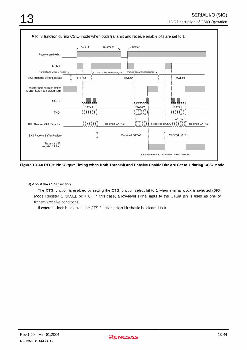
SERIAL I/O (SIO) 13.3 Description of CSIO Operation
Rev.1.00 Mar 01,2004 13-44
REJ09B0134-0001Z
13
RTS function during CSIO mode when both transmit and receive enable bits are set to 1
Receive enable bit
DATA1
TXDi
RTSi#
Set to 1
DATA3
SIOi Transmit Buffer Register
Transmit shift register empty (transmission completed flag)
DATA2 DATA3
SCLKi
Set to 1 Cleared to 0
Transmit data written to register Transmit data written to register
DATA1
DATA2
Transmit data written to register
SIOi Receive Shift Register
DATA3
Received DATA1 Received DATA2 Received DATA3
SIOi Receive Buffer Register Received DATA1 Received DATA2
Transmit shift register full flag
Data read from SIOi Receive Buffer Register
Figure 13.3.8 RTSi# Pin Output Timing when Both Transmit and Receive Enable Bits are Set to 1 during CSIO Mode
(3) About the CTS function
The CTS function is enabled by setting the CTS function select bit to 1 when internal clock is selected (SIOi Mode Register 1 CKSEL bit = 0). In this case, a low-level signal input to the CTSi# pin is used as one of transmit/receive conditions.
If external clock is selected, the CTS function select bit should be cleared to 0.

SERIAL I/O (SIO) 13.3 Description of CSIO Operation
Rev.1.00 Mar 01,2004 13-45
REJ09B0134-0001Z
13 13.3.7 Example Transmit/Receive (Full Duplex) Timing during CSIO Mode
Figure 13.3.9 shows an example transmit/receive (full duplex) timing when internal clock is selected and the CTS function is enabled.
Figure 13.3.10 shows an example transmit/receive (full duplex) timing when internal clock is selected and the RTS function is enabled.
Example timing (internal clock)
Transmit and receive enable bitsNote 1
DATA1
CTSi# Note 2
SIOi Receive Buffer Register
Set to 1
TXDi Note 3
Receive shift register full flag
Reception completed flag
Transmit/receive clock (SCLKi)
D8
DATA4 DATA5
DATA2
Reception-completed processingrequest output (internal signal)
Wait for low level input to CTSi#
SCLKi
CTSi#
SCLK
RTS# or PORT
Internal clock selected
Note 1: If an overrun error occurs, the transmit and receive enable bits are cleared to 0. Note 2: The status in the section is “Don’t Care.” Note 3: This applies to the case where data is transmitted LSB first. If MSB first, data is transmitted in order of D8, D9–D14 and D15. Note 4: For details about transmit buffer empty processing and transmission-completed interrupt requests, refer to Section 13.2.5, “SIOi Transfer Processing Control
Registers.”
SIOi Receive Shift Register DATA4
DATA3
D15 D14 D13 D12 D11 D10 D9 D8
DATA5
D15 D14 D13 D12 D11 D10 D9 D8
DATA6
D15 D14 D13 D12 D11 D10 D9
Wait for SIOi Receive Buffer Register to be read out
Processing request for DATA5
TXD
RXDi RXD
TXDi
DATA2 DATA3 SIOi Transmit Buffer Register
Transmit data written to register
DATA1
Transmit data written to register Transmit data written to register
Cleared to 0 during transmission/reception
Transmit buffer empty flag
Transferred to transmit shift register because transmit condition on the transmit side is met
Transmission completed flag
Transmit buffer empty processing request output
(internal signal)
Not set because condition for data transfer to the SIOi Transmit Shift Register is met
Transmission-completed interrupt request output
(internal signal) Not output because the next transmit data already written to the register
DATA4
RXDi Note 3D8
DATA5 DATA3
D15 D14 D13 D12 D11 D10 D9 D8D15 D14 D13 D12 D11 D10 D9 D8 D15 D14 D13 D12 D11 D10 D9
Data read from SIOi Receive Buffer Register
Processing request for DATA4
Not cleared because received data already prepared in SIOi Receive Shift Register
Figure 13.3.9 Example Transmit/Receive (Full Duplex) Timing in CSIO Mode 1 (when Internal Clock Selected and the
CTS Function Enabled)

SERIAL I/O (SIO) 13.3 Description of CSIO Operation
Rev.1.00 Mar 01,2004 13-46
REJ09B0134-0001Z
13
Example timing (external clock)
Transmit and receive enable bitsNote 1
DATA1
RTSi#
SIOi Receive Buffer Register
Set to 1
TXDi Note 2
Receive shift register full flag
Reception completed flag
Transmit/receive clock (SCLKi)
D8
DATA4 DATA5
DATA2
Reception-completed processingrequest output (internal signal)
Wait for input to SCLKi
SCLKi
RTSi#
SCLK
CTS# or PORT
External clock selected
Note 1: If an overrun error occurs, the transmit and receive enable bits are cleared to 0. Note 2: This applies to the case where data is transmitted LSB first. If MSB first, data is transmitted in order of D8, D9–D14 and D15. Note 3: For details about transmit buffer empty processing and transmission-completed interrupt requests, refer to Section 13.2.5, “SIOi Transfer Processing Control Registers.”
SIOi Receive Shift Register DATA4
DATA3
D15 D14 D13 D12 D11 D10 D9 D8
DATA5
D15 D14 D13 D12 D11 D10 D9 D8
DATA6
D15 D14 D13 D12 D11 D10 D9
Wait for SIOi Receive Buffer Register to be read out
Processing request for DATA5
TXD
RXDi RXD
TXDi
DATA2 DATA3 SIOi Transmit Buffer Register
Transmit data written to register
DATA1
Transmit data written to register Transmit data written to register
Cleared to 0 during transmission/reception
Transmit buffer empty flag
Transmission completed flag
Transmit buffer empty processing request output
(internal signal)
Not set because condition for data transfer to the SIOi Transmit Shift Register is met
Transmission-completed interrupt request output
(internal signal) Not output because the next transmit data already written to the register
DATA4
RXDi Note 2D8
DATA5 DATA3
D15 D14 D13 D12 D11 D10 D9 D8D15 D14 D13 D12 D11 D10 D9 D8 D15 D14 D13 D12 D11 D10 D9
Data read from SIOi Receive Buffer Register
Processing request for DATA4
Not cleared because received data already prepared in SIOi Receive Shift Register
Figure 13.3.10 Example Transmit/Receive (Full Duplex) Timing in CSIO Mode 2 (when External Clock Selected and
the RTS Function Enabled)

SERIAL I/O (SIO) 13.3 Description of CSIO Operation
Rev.1.00 Mar 01,2004 13-47
REJ09B0134-0001Z
13 13.3.8 Example Initial Settings during CSIO
Figure 13.3.11 shows an example of how to initialize the CSIO mode related registers.
CSIO initialization
Set Input/output Port Operation Mode Register
Set SIOi Mode Registers 0 and 1 Set to CSIO mode Set handshaking functions (RTS#, CTS#) Set character length Select internal/external clock Select peripheral I/O clock/fixed frequency clock Select CMOS output/N-ch open-drain output Select LSB/MSB first
Set SIOi Baud Rate Register Baud rate divide-by value (H’0000 0000 to H’0000 FFFF) (when internal clock selected)
Set SIOi Transfer Processing Control Register
Enable/disable transmission-completed (transmit shift register empty) interrupt Select requested processing when transmit buffer empty Select requested processing when reception completed (receive buffer full) Disable/enable interrupt for receive error
SIO registers
Set Interrupt Controller and SIOi Transmit Interrupt Control Register (When using interrupts)
Set DMAC related registers (When using DMAC)
End of CSIO initialization
Figure 13.3.11 Example Initial Settings in CSIO Mode

SERIAL I/O (SIO) 13.4 Description of UART Operation
Rev.1.00 Mar 01,2004 13-48
REJ09B0134-0001Z
13 13.4 Description of UART Operation
The following describes device operation in UART mode.
13.4.1 Data Transfer Rate (Baud Rate) in UART
The data transfer rate (baud rate) in UART mode is determined by the transfer clock.
(1) When internal clock is selected
The internal clock (PCLK) is divided by n + 1 where n = the value set by the SIOi Baud Rate Register. The “divided by n + 1” count source is further divided by 16 and a correction value set by the SIOi Baud Rate Correction Register is added, to produce the transfer clock.
f(PCLK)
Baud rate (bps) = (value set by the SIOi Baud Rate Register + 1) × 16 + baud rate correction value
Note 1: Values set by the SIOi Baud Rate Register = H’0000 0000 to H’0000 FFFF
Note 2: Baud rate correction values = 0, 2, 4, 6, 8, 10, 12 or 14
(2) When external clock is selected
External clock cannot be used. Setting CKSEL = 1 is prohibited.
13.4.2 UART Mode Transmit Operation
(1) Data transmit conditions
When all of the following conditions are met, the transmit data is transferred from the SIOi Transmit Buffer Register to the SIOi Transmit Shift Register. The transmit data transferred to the SIOi Transmit Shift Register is transmitted from the TXDi pin.
The input signal to the CTSi# pin is asserted low (when CTS function is enabled) Transmit enable bit = 1 Data exists in the SIOi Transmit Buffer Register (SIOi Status Register TEMP bit = 0) No data exists in the SIOi Transmit Shift Register (SIOi Status Register TXCP bit = 1)
(2) About the RTS function
The RTS function is not used for transmit operation in UART mode.
(3) About the CTS function
The CTS function is enabled by setting the CTS function select bit (SIOi Mode Register 0 CTSS bit) to 1. A low-level signal input to the CTSi# pin is used as one of transmit conditions.

SERIAL I/O (SIO) 13.4 Description of UART Operation
Rev.1.00 Mar 01,2004 13-49
REJ09B0134-0001Z
13
13.4.3 Example Transmit Timing during UART Mode
Figure 13.4.1 shows an example transmit timing when the CTS function is enabled.
Example timing (transfer data format: 1 start bit, 7-bit data, 1 stop bit)
Transmit enable bit
DATA1
CTSi# Note 1
Set to 1
TXDi Note 2
Transmit buffer empty flag
Transmission completed flag
SP
DATA2
Transmission-completed interruptrequest output (internal signal)
Wait for low level input to CTS#
Not set because condition for data transfer to the SIOi Transmit Shift Register is met
CTSi# RTS# or PORT
DATA3
D15 D14 D13 D12 D11 D10 D9
Transmit buffer empty processing request output (internal signal)
RXD
TXDi
ST
DATA1
SPD15 D14 D13 D12 D11 D10 D9ST
SIOi Transmit Buffer Register
SP D15 D14 D13 D12 D11 D10 D9 ST
DATA2 DATA3
Cleared to 0 during transmission
Transmit data written to register Transmit data written to register Transmit data written to register
Not output because the next transmit data already written to the register
Note 1: The status in the section is “Don’t Care.” Note 2: This applies to the case where data is transmitted LSB first. Note 3: For details about transmit buffer empty processing and transmission-completed interrupt requests, refer to Section 13.2.5, “SIOi Transfer
Processing Control Registers.”
Figure 13.4.1 Example Transmit Timing in UART Mode (When CTS Function Enabled)

SERIAL I/O (SIO) 13.4 Description of UART Operation
Rev.1.00 Mar 01,2004 13-50
REJ09B0134-0001Z
13
13.4.4 UART Mode Receive Operation
(1) Data receive conditions
When all of the following conditions are met, the received data is taken from the RXDi pin into the SIOi Receive Shift Register, and when all bits of data are prepared in the SIOi Receive Shift Register, the received data is transferred from the SIOi Receive Shift Register to the SIOi Receive Buffer Register.
Receive enable bit = 1 The falling edge of the start bit (ST) is detectedNote
Note: If the start bit is detected high when sampled again after the falling edge of the start bit was detected, erroneous start bit determination is assumed and the receive operation is forcibly stopped, thereafter waiting for start bit input again. For the start bit detection point, refer to Section 13.5.3, “Precautions to Be Taken for Serial I/O.”
(2) About the RTS function
The signal output from the RTSi# pin is pulled low to indicate to the connected device that SIO is ready to receive. The timing at which the RTSi# pin changes state depends on how the RTS timing select bit is set.
<If the RTS timing select bit = 0>
When one of the following conditions is met, the RTSi# pin changes state from high to low. The receive enable bit is set to 1 while “no data exists” in the SIOi Receive Shift Register Data in the SIOi Receive Shift Register has gone while the receive enable bit = 1
When one of the following conditions is met, the RTSi# pin changes state from low to high. The receive enable bit is cleared to 0 (explicitly or by a receive error) A start bit is received while “data exists” in the SIOi Receive Buffer Register” and “no data exists” in the
SIOi Receive Shift Register
<If the RTS timing select bit = 1>
When one of the following conditions is met, the RTSi# pin changes state from high to low. The receive enable bit is set to 1 while “no data exists” in the SIOi Receive Buffer Register Data in the SIOi Receive Buffer Register has gone while the receive enable bit = 1
When one of the following conditions is met, the RTSi# pin changes state from low to high. The receive enable bit is cleared to 0 (explicitly or by a receive error) A start bit is received
Figure 13.4.2 shows RTSi# pin output timing during UART mode.

SERIAL I/O (SIO) 13.4 Description of UART Operation
Rev.1.00 Mar 01,2004 13-51
REJ09B0134-0001Z
13
RTS function during UART mode
<When RTS timing select bit = 0>
Receive enable bit
DATA1
RXDi
RTSi#
Set to 1
ST
SP
SIOi Receive Shift Register
DATA2
ST
SP DATA3
ST
SP DATA4
ST
SP
DATA1 DATA2 DATA3 DATA4
SIOi Receive Buffer Register
Receive shift register full flag
DATA1 DATA2 DATA3
Data read from SIOi Receive Buffer Register Data read from SIOi Receive Buffer Register
Receive enable bit
DATA1
RXDi
RTSi#
Set to 1
ST
SP
SIOi Receive Shift Register
DATA2
ST
SP
SIOi Receive Buffer Register
Receive shift registerfull flag
DATA1 DATA2
Data read from SIOi Receive Buffer Register
<When RTS timing select bit = 1>
DATA1 DATA2
Set to 1 Cleared to 0
“0”
Figure 13.4.2 RTS# Pin Output Timing during UART Mode

SERIAL I/O (SIO) 13.4 Description of UART Operation
Rev.1.00 Mar 01,2004 13-52
REJ09B0134-0001Z
13
13.4.5 Example UART Mode Receive Timing
Figure 13.4.3 shows an example receive timing when the RTS function is enabled.
Example timing (transfer data format: 1 start bit, 7-bit data, 1 stop bit)
Receive enable bit
DATA1
RTSi# Note 1
SIOi Receive Buffer Register
Set to 1
RXDi Note 2
Receive shift register full flag
Reception completed flag
SP
DATA1
DATA2
Reception-completed processing request output
(internal signal)
Wait for receive data
Data read from SIOi Receive Buffer Register
RTSi# CTS# or PORT
Note 1: This is the timing when RTS timing select bit = 0. Note 2: This applies to the case where data is transmitted LSB first. Note 3: For details about transmit buffer empty processing and transmission-completed interrupt requests, refer to Section 13.2.5, “SIOi Transfer
Processing Control Registers.”
SIOi Receive Shift Register DATA1
DATA3
D15 D14 D13 D12 D11 D10 D9
DATA2
DATA3
Receive overrun error flag
Receive error interrupt requestoutput (internal signal)
Processing request for DATA1 Processing request for DATA2
TXD
RXDi
ST SPD15 D14 D13 D12 D11 D10 D9ST D15 D14 D13 ST
Set to 1 Cleared to 0
Figure 13.4.3 Example Receive Timing in UART Mode (when RTS Function Enabled)

SERIAL I/O (SIO) 13.4 Description of UART Operation
Rev.1.00 Mar 01,2004 13-53
REJ09B0134-0001Z
13
13.4.6 UART Mode Transmit/Receive Operation
Transmit/receive conditions in UART mode are independent on the transmit and the receive sides. For details about timing, refer to Figure 13.4.1, “Example Transmit Timing in UART Mode (When CTS Function Enabled),” and Figure 13.4.3, “Example Receive Timing in UART Mode (when RTS Function Enabled).”
Figure 13.4.4 shows an example transmit/receive connection in UART mode.
CTSi# RTS# or PORT
TXD
RXDi RXD
TXDi
RTSi# CTS# or PORT
Figure 13.4.4 Example Transmit/Receive Connection in UART Mode (when CTS/RTS Functions Enabled)

SERIAL I/O (SIO) 13.4 Description of UART Operation
Rev.1.00 Mar 01,2004 13-54
REJ09B0134-0001Z
13
13.4.7 Example Initial Settings during UART Mode
Figure 13.4.5 shows an example of how to initialize the UART mode related registers.
UART initialization
Set Input/output Port Operation Mode Register
Set SIOi Mode Registers 0 and 1
Set to UART mode Set handshaking functions (RTS#, CTS#) Set character length Set parity Set transmit/receive stop bit Set internal clock Select CMOS output/N-ch open-drain output Select LSB/MSB first
Set SIOi Baud Rate Register Baud rate divide-by value (H’0000 0000 to H’0000 FFFF)
Set SIOi Transfer Processing Control Register
Enable/disable transmission-completed (transmit shift register empty) interrupt Select requested processing when transmit buffer empty Select requested processing when reception completed(receive buffer full) Disable/enable interrupt for receive error
SIO registers
Set Interrupt Controller and SIOi Transmit Interrupt Control Register (When using interrupts)
Set DMAC related registers (When using DMAC)
End of UART
Set SIOi Baud Rate Correction Register Baud rate correction value (0, 2, 4, 6, 8, 10, 12 or 14)
Figure 13.4.5 Example Initial Settings in UART Mode

SERIAL I/O (SIO) 13.5 Precautions to Be Taken for Serial I/O
Rev.1.00 Mar 01,2004 13-55
REJ09B0134-0001Z
13
13.5 Precautions to Be Taken for Serial I/O 13.5.1 Precautions Common to CSIO and UART Modes
Make sure that SIOi Mode Registers 0 and 1, the SIOi Interrupt Mask Register, SIOi Baud Rate Register and SIOi Baud Rate Correction Register are set while SIO is idle (transmit and receive enable bits both disabled, with no data being transmitted or received).
Make sure the receive status initialization bit (RSCLR) in the SIOi Control Register is set when reception is disabled (RXEN = 0) and no data is being received (RXSC = 0). (Do not set the receive status initialization bit and the receive enable bit at the same time.)
Make sure the transmit status initialization bit (TSCLR) in the SIOi Control Register is set when transmission is disabled (TXEN = 0) and no data is being transmitted (TXSC = 0). (Do not set the transmit status initialization bit and the transmit enable bit at the same time.)
If the receive enable bit is set to 1 when any receive error flag is set, device operation cannot be guaranteed.
13.5.2 Precautions to Be Taken during CSIO Mode
If an overrun error occurs, the transmit and receive enable bits are cleared, with transmit/receive operations stopped thereafter. Therefore, the transmit and receive enable bits should be reenabled in software, to receive the previously received data over again.
If internal clock is selected and N-ch open-drain output is selected for the TXDi pin output mode in CSIO mode, the TXDi pin is placed in the high-impedance state a half transfer clock period after the last rise of the transfer clock. If external clock is selected, the TXDi pin operates as CMOS output no matter how the TXDi pin output mode select bit is set.
If the transfer clock source is changed from external clock to internal clock after a transfer with external clock in CSIO mode has finished, a low pulse may be output for 1 PCLK period from the SCLKi pin. Therefore, follow the procedure described below to change CKSEL settings from external clock to internal clock.
<Setup procedure>
(1) After confirming that a transfer with external clock in CSIO mode has finished (transmit enable bit = 0 and receive
enable bit = 0 and the SIOi Status Register receive shift register status flag = 0 and transmit shit register status
flag = 0),
(2) Change the SCLKi pin for port (by setting the Port Pi Operation Mode Register).
(3) Select CSIO mode and internal clock.
(4) Change the pin set for port back to the SCLKi pin (by setting the Port Pi Operation Mode Register).

SERIAL I/O (SIO) 13.5 Precautions to Be Taken for Serial I/O
Rev.1.00 Mar 01,2004 13-56
REJ09B0134-0001Z
13
13.5.3 Precautions to Be Taken during UART Mode
If an overrun error occurs, the receive enable bit is cleared, with receive operation stopped thereafter. Therefore, the receive enable bit should be reenabled in software, to receive the previously received data over again.
To detect the receive start bit, the SIO samples the RXDi signal again after detecting a falling edge of the RXDi signal. If the RXDi signal is detected high when sampled again, erroneous start bit determination is assumed and the receive operation is forcibly stopped, thereafter waiting for start bit input again. It is at an intermediate point of the start bit (half a 1 bit transfer time after the first sampled point) that the start bit is sampled again. If the receive enable bit (SIOi Control Register RXEN bit) is cleared to 0 before the start bit is sampled again after detecting a falling edge of the RXDi signal, device operation cannot be guaranteed.
If N-ch open-drain output is selected for the TXDi pin output mode in UART mode, the TXDi pin outputs a low for the start bit and goes to a high-impedance state for the stop bit.
The stop bit is detected at an intermediate point of the stop bit (half a 1 bit transfer time later). If the RXDi pin goes low immediately after detecting the stop bit, no framing errors are assumed, and SIO starts a receive operation recognizing it as the start bit of the next data.

CHAPTER 14ON-CHIP USER IP BUS CHAPTER 14
ON-CHIP USER IP BUS

ON-CHIP USER IP BUS 14.1 Outline of the On-chip User IP Bus
Rev.1.00 Mar 01,2004 14-2
REJ09B0134-0100Z
14 14.1 Outline of the On-chip User IP Bus
Operations of the on-chip user IP bus include the following: (1) CPU access (2) DMA access
• Fly-by transfer mode • Dual-address transfer mode
14.2 On-chip User IP Bus Related Signals Table 14.2.1 lists the signals associated with the on-chip user IP bus.
Table 14.2.1 On-chip User IP Bus Related Signals
Symbol Signal Name Type Function
IPMS
Module select Input Indicates access to the user IP module. It is effective during CPU access and dual-address mode DMA access.
IPAB Address bus Input Indicates the internal register address of the user IP module. It is effective during CPU access and dual-address mode DMA access.
IPRS
Read strobe Input Indicates the read timing during read access. It is effective during CPU access and dual-address mode DMA access.
IPWS0–IPWS3
Write strobe Input Indicates the write timing during write access. It is effective during CPU access and dual-address mode DMA access.
IPREADY Ready Output Wait cycles can be added depending on the output timing of this signal. It is effective during CPU access and dual-address mode DMA access.
DREQ1 DMA request Output Sends a DMA transfer request to the OPSP. DACK1 DMA acknowledge Input Indicates that the OPSP has accepted the DMA transfer
request sent from the user IP module. IPFBMODE Fly-by mode Input Indicates that DMA transfer is performed in fly-by mode.IPFBRS Fly-by read strobe Input Indicates the read timing during read access.
It is effective during fly-by mode DMA access. IPFBWS Fly-by write strobe Input Indicates the write timing during write access.
It is effective during fly-by mode DMA access. IPRDB0–IPRDB31 Read data bus Output This is the data bus for read from the user IP module. IPWDB0–IPWDB31 Write data bus Input This is the data bus for write to the user IP module.
Note: The input/output directions in this table are relative to the user IP module. Therefore, “input” in this table refers to input to the user IP module, and “output” refers to output from the user IP module.

ON-CHIP USER IP BUS 14.3 Operation of the On-chip User IP Bus
Rev.1.00 Mar 01,2004 14-3
REJ09B0134-0100Z
14 14.3 Operation of the On-chip User IP Bus 14.3.1 CPU Access
Figure 14.3.1 shows an operation for read from the on-chip user IP bus by the CPU. Figure 14.3.2 shows an operation for write to the on-chip user IP bus by the CPU.
"L"
Zero wait access N wait access
don't care Module sampling CPU core sampling
Note 1
Note 2 Note 2
Note 1: The next access may start two cycles later in the shortest case. Note 2: During this period, a selected module drives IPREADY and IPRDB.
N cycles
IPMS
IPWS
IPRS
IPREADY
DREQ1
IPAB
IPRDB
DACK1
IPFBRS
IPFBWS
IPFBMODE
IPWDB
BCLK
"L"
"L"
"L"
"L"
"L"
Figure 14.3.1 CPU Access (Register Read)

ON-CHIP USER IP BUS 14.3 Operation of the On-chip User IP Bus
Rev.1.00 Mar 01,2004 14-4
REJ09B0134-0100Z
14
"L"
don't care Module sampling CPU core sampling
Note 1
Note 2 Note 2
Note 1: The next access may start two cycles later in the shortest case. Note 2: During this period, a selected module drives IPREADY and IPRDB.
N cycles
IPMS
IPWS
IPRS
IPREADY
DREQ1
IPAB
IPRDB
DACK1
IPFBRS
IPFBWS
IPFBMODE
IPWDB
BCLK
"L"
"L"
"L"
"L"
"L"
Zero wait access N wait access
Figure 14.3.2 CPU Access (Register Write)

ON-CHIP USER IP BUS 14.3 Operation of the On-chip User IP Bus
Rev.1.00 Mar 01,2004 14-5
REJ09B0134-0100Z
14 14.3.2 DMA Access
Accesses to the on-chip user IP bus by the DMAC are performed in one of the following two modes: • Fly-by mode • Dual-address mode
(1) Access in fly-by mode
Figure 14.3.3 shows a fly-by read operation by the DMAC. Figure 14.3.4 shows a fly-by write operation by the DMAC.
"L"
Module sampling CPU core sampling
Note 1
IPMS
IPWS
IPRS
IPREADY
DREQ1
IPAB
IPRDB
DACK1
IPFBRS
IPFBWS
IPFBMODE
IPWDB
BCLK
Note 1: The number of cycles varies depending on condition. (0 BCLK in the shortest case) Note 2: The next access may start one cycle later in the shortest case. Note 3: During this period, the module selected by DACK1 drives IPRDB.
"L"
"L"
"L"
Note 2
Note 1
Note 3 Note 3
Figure 14.3.3 DMA Access (Read in Fly-by Mode)

ON-CHIP USER IP BUS 14.3 Operation of the On-chip User IP Bus
Rev.1.00 Mar 01,2004 14-6
REJ09B0134-0100Z
14
"L"
Module sampling
Note 2
Note 1: The number of cycles varies depending on condition. (Two cycles in the shortest case) Note 2: The next access may start one cycle later in the shortest case.
Note 1
IPMS
IPWS
IPRS
IPREADY
DMREQ1
IPAB
IPRDB
DMACK1
IPFBRS
IPFBWS
IPFBMODE
IPWDB
BCLK
"L"
"L"
"L"
Figure 14.3.4 DMA Access (Write in Fly-by Mode)

ON-CHIP USER IP BUS 14.3 Operation of the On-chip User IP Bus
Rev.1.00 Mar 01,2004 14-7
REJ09B0134-0100Z
14 (2) Access in dual-address mode
Figure 14.3.5 shows a read operation in dual-address mode by the DMAC. Figure 14.3.6 shows a write operation in dual-address mode by the DMAC.
"L"
don't care Module sampling OPSP sampling
Note 1
Note 2
Note 1: The next access may start two cycles later in the shortest case. Note 2: During this period, the module selected by IPMS drives IPREADY and IPRDB.
IPMS
IPWS
IPRS
IPREADY
DREQ1
IPAB
IPRDB
DACK1
IPFBRS
IPFBWS
IPFBMODE
IPWDB
BCLK
"L"
"L"
"L"
Note 2
Figure 14.3.5 DMA Access (Read in Dual-address Mode)

ON-CHIP USER IP BUS 14.3 Operation of the On-chip User IP Bus
Rev.1.00 Mar 01,2004 14-8
REJ09B0134-0100Z
14
"L"
don't care Module sampling OPSP sampling
Note 1: The next access may start two cycles later in the shortest case. Note 2: During this period, the module selected by IPMS drives IPREADY.
Note 2
IPMS
IPWS
IPRS
IPREADY
DREQ1
IPAB
IPRDB
DACK1
IPFBRS
IPFBWS
IPFBMODE
IPWDB
BCLK
"L"
"L"
"L"
Note 2
Note 1
Figure 14.3.6 DMA Access (Write in Dual-address Mode)

ON-CHIP USER IP BUS 14.4 Setting Up the Block Select Controller
Rev.1.00 Mar 01,2004 14-9
REJ09B0134-0100Z
14 14.4 Setting Up the Block Select Controller
To access the on-chip user IP bus, the Block Select Controller should be set up. The following control registers in
the Block Select Controller are used for block 1. Set the values listed in Table 14.4.1 through Table 14.4.3 in these registers. If any other values are set, operation of the on-chip user IP bus cannot be guaranteed.
BSEL1 Control Register 0 BSEL1 Control Register 1 BSEL1 Control Register 2
Table 14.4.1 Set Values of BSEL1 Control Register 0
Bit Name Set Value Setting
RWAIT Read software wait cycles select bits
"00001" 1BCLK
WWAIT Write software wait cycles select bits
"00001" 1BCLK
RDYSEL External READY wait select bit
"1" Insert external READY wait
PRWAIT Page read software wait cycles select bits
"00000" 0BCLK
STBWAIT Strobe output wait cycles select bits
"00" At the same time as BSEL1# signal
PWWAIT Page write software wait cycles select bits
"00000" 0BCLK
Table 14.4.2 Set Values of BSEL1 Control Register 1
Bit Name Set Value Setting
PAEN Page access enable bit
"0" Disable page access
BSZ Bus size select bits
"10" 32 bits
BWAIT BSEL wait cycles select bits
"00" 0BCLK
RRECWAIT Read recovery cycles select bits
"00" 0BCLK
WRECWAIT Write recovery cycles select bits
"00" 0BCLK
NWAIT Next access wait cycles select bits
"0001" 1BCLK
Table 14.4.3 Set Values of BSEL1 Control Register 2
Bit Name Set Value Setting
RDYCNT READY polarity control bit
"1" Use the READY# signal as active-high.

ON-CHIP USER IP BUS 14.4 Setting Up the Block Select Controller
Rev.1.00 Mar 01,2004 14-10
REJ09B0134-0100Z
14
This page is blank for reasons of layout

CHAPTER 15CLOCK & POWER MANAGER (CPM) CHAPTER 15
CLOCK & POWER MANAGER (CPM)

CLOCK & POWER MANAGER (CPM) 15.1 Outline of the Clock & Power Manager
Rev.1.00 Mar 01,2004 15-2
REJ09B0134-0100Z
15 15.1 Outline of the Clock & Power Manager
The clock & power management function manages clock waveform generation and low power consumption mode. There are following three clock operation modes:
Normal operation mode CPU sleep mode Standby mode
Table 15.1.1 Relationship between Clock Modes and Clocks
Clock Mode CPU Clock Peripheral IO Clock/ BCLK Entering and Exiting Each Mode
Normal operation mode Supplied Supplied
CPU sleep mode Stopped Supplied Entered by setting the low power consumption mode
select bit
Exited by external INT, peripheral IO interrupt or
SBI#
Standby mode Stopped Stopped Entered by setting the low power consumption mode
select bit
Exited by WKUP#
15.1.1 Clock System
The OPSP has three discrete clocks, which are listed in Table 15.1.2. Note, however, that the frequency multiplier (PLL), phase adjust circuit (DLL) and clock divider depend on
implementation. Figure 15.1.1 shows a reference block diagram of the clock system in which the frequency multiplier (PLL), phase adjust circuit (DLL) and clock divider are implemented.
The operating frequency of each clock should be set to meet the conditions given below.
Conditions for the operating frequency of each clock f(CPUCLK) ≥ f(PCLK) = f(BCLK)
Table 15.1.2 Clock System of the OPSP
Type of Clock Reference Clock for Each Clock
Function
1 CPUCLK (CPU clock)
CLKIN Reference clock for the CPU core, internal memory and caches
2 BCLK (system clock)
CPUCLK Reference clock for operation of the internal peripheral I/O (bus control circuit) and for the external data bus and user I/P module
3 PCLK (peripheral I/O clock)
CPUCLK Reference clock for SFR access and operation of the internal peripheral I/O (not including the bus control circuit)

CLOCK & POWER MANAGER (CPM) 15.1 Outline of the Clock & Power Manager
Rev.1.00 Mar 01,2004 15-3
REJ09B0134-0100Z
15 PLL(x8) Not divided
1/2
1/4
1/8
DLL
CLKIN
BCLKOUT
BCLKIN
CPU clock
(Up to 200MHz)
Peripheral I/O clock
(Up to 100MHz)Not divided
1/2
1/4
1/8
Not divided
1/2
1/4
1/8
BCLK (Up to 100MHz)
Divided clock frequency select (DIVSEL)
BCLK/ peripheral I/O clock divide ratio select
(PDIV)Same value is set.
Figure 15.1.1 Reference Block Diagram of the Clock System

CLOCK & POWER MANAGER (CPM) 15.2 Clock & Power Manager Related Registers
Rev.1.00 Mar 01,2004 15-4
REJ09B0134-0100Z
15 15.2 Clock & Power Manager Related Registers
The following shows a memory map of the Clock & Power Manager related registers and describes each register.
Clock & Power Manager Register Mapping
Address b0 +0 address b7 b8 +1 address b15 b16 +2 address b23 b24 +3 address b31
H'00EF 4000 Clock Control Register Note (CLKCR)
H'00EF 4004 PLL Control Register (PLLCR)
H'00EF 4008 Clock Mode Register Note (CLKMOD)
H'00EF 400C BCLK Divide Ratio Select Register Note (BCLKDIV)
Note: These are example registers shown for reference. Each function of the frequency multiplier (PLL), phase adjust circuit (DLL) and clock divider are implementation-dependent.

CLOCK & POWER MANAGER (CPM) 15.2 Clock & Power Manager Related Registers
Rev.1.00 Mar 01,2004 15-5
REJ09B0134-0100Z
15 15.2.1 Clock Control Register
Clock Control Register (CLKCR) <Address: H’00EF 4000>
b0 1 2 3 4 5 6 7 8 9 10 11 12 13 14 b15
0 0 0 0 0 0 0 0 0 0 0 0 0 0 0 0
b16 17 18 19 20 21 22 23 24 25 26 27 28 29 30 b31
CLKSEL DIVSEL 0 0 0 0 0 0 0 0 0 0 0 0 0 0 0 0
<After reset: H’0000 0000>
b Bit Name Function R W
0–22 No functions assigned. Fix these bits to 0. 0 0
23 CLKSEL CPUCLK select bit
0: f(CLKIN) 1: PLL clock Note 1
R W
24–29 No functions assigned. Fix these bits to 0. 0 0
30–31 DIVSEL Divided clock frequency select bits
00: Not divided 01: Divided by 2 10: Divided by 4 11: Divided by 8
R W
Note 1: To select PLL clock, set the PLL operation enable bit (PLL Control Register bit 31) to 1 and then set this bit after the
PLL is locked in phase.
(1) CLKSEL (CPUCLK select) bit (b23)
This bit selects the CPUCLK (CPU clock).
To select PLL clock, set the PLL operation enable bit (PLL Control Register bit 31) to 1 and then set this bit
after the PLL is locked in phase.
(2) DIVSEL (divided clock frequency select) bits (b30, b31)
These bits select a divided clock frequency of CPUCLK (CPU clock).
Table 15.2.1 CPUCLK (CPU Clock) Frequency Settings
CLKSEL bit DIVSEL bit CPUCLK (CPU clock)
"0" "00" f(CLKIN) "0" "01" f(CLKIN) / 2 "0" "10" f(CLKIN) / 4 "0" "11" f(CLKIN) / 8 "1" "00" x8 f(CLKIN) "1" "01" x8 f(CLKIN) / 2 "1" "10" x8 f(CLKIN) / 4 "1" "11" x8 f(CLKIN) / 8

CLOCK & POWER MANAGER (CPM) 15.2 Clock & Power Manager Related Registers
Rev.1.00 Mar 01,2004 15-6
REJ09B0134-0100Z
15 15.2.2 PLL Control Register
PLL Control Register (PLLCR) <Address: H’00EF 4004>
b0 1 2 3 4 5 6 7 8 9 10 11 12 13 14 b15
0 0 0 0 0 0 0 0 0 0 0 0 0 0 0 0
b16 17 18 19 20 21 22 23 24 25 26 27 28 29 30 b31
PLLEN0 0 0 0 0 0 0 0 0 0 0 0 0 0 0 0
<After reset: H’0000 0000>
b Bit Name Function R W
0–30 No functions assigned. Fix these bits to 0. 0 0
31 PLLEN PLL operation enable bit
0: Stop PLL 1: PLL clock Note 1
R W
(1) PLLEN (PLL operation enable) bit (b31)
This bit selects to enable or stop PLL clock. To use PLL clock, set this bit to 1 and then set the CPUCLK select
bit to 1 after the PLL is locked in phase.

CLOCK & POWER MANAGER (CPM) 15.2 Clock & Power Manager Related Registers
Rev.1.00 Mar 01,2004 15-7
REJ09B0134-0100Z
15 15.2.3 Clock Mode Register
Clock Mode Register (CLKMOD) <Address: H’00EF 4008>
b0 1 2 3 4 5 6 7 8 9 10 11 12 13 14 b15
0 0 0 0 0 0 0 0 0 0 0 0 0 0 0 0
b16 17 18 19 20 21 22 23 24 25 26 27 28 29 30 b31
PMSEL 0 0 0 0 0 0 0 0 0 0 0 0 0 0 0 0
<After reset: H’0000 0000>
b Bit Name Function R W
0–29 No functions assigned. Fix these bits to 0. 0 0
30–31 PMSEL Low power consumption mode select bits
00: Normal operation mode 01: CPU sleep mode 10: Standby mode 11: Setting prohibited
R W
(1) PMSEL (low power consumption mode select) bits (b30, b31)
These bits select low power consumption mode.
CPU sleep mode is entered into by setting the PMSEL bits to ‘01.’ If a request to exit (e.g., INT0–INT7 interrupt
request, internal peripheral I/O interrupt request or system break interrupt request) occurs during CPU sleep
mode, these bits are cleared to 0 and normal operation mode returns.
Standby mode is entered into by setting the PMSEL bits to ‘10.’ If a wakeup interrupt request (WKUP#) or
reset request (RESET#) occurs during standby mode, these bits are cleared to ‘00’ and normal operation mode
returns.

CLOCK & POWER MANAGER (CPM) 15.2 Clock & Power Manager Related Registers
Rev.1.00 Mar 01,2004 15-8
REJ09B0134-0100Z
15 15.2.4 BCLK Divide Ratio Select Register
BCLK Divide Ratio Select Register (BCLKDIV) <Address: H’00EF 400C>
b0 1 2 3 4 5 6 7 8 9 10 11 12 13 14 b15
0 0 0 0 0 0 0 0 0 0 0 0 0 0 0 0
b16 17 18 19 20 21 22 23 24 25 26 27 28 29 30 b31
PDIV 0 0 0 0 0 0 0 0 0 0 0 0 0 0 1 1
<After reset: H’0000 0003>
b Bit Name Function R W
0–29 No functions assigned. Fix these bits to 0. 0 0
30–31 PDIV BCLK/ PCLK divide ratio select
00: f(CPUCLK) 01: f(CPUCLK)/2 10: f(CPUCLK)/4 11: f(CPUCLK)/8
R W
(1) BCLKDIV (BCLK/ PCLK divide ratio select) bits (b30, b31)
These bits select the divide ratio of BCLK (system clock) and PCLK (peripheral IO clock).

CHAPTER 16COPROCESSOR INTERFACE CHAPTER 16
COPROCESSOR INTERFACE

COPROCESSOR INTERFACE 16.1 Outline of the Coprocessor Interface
Rev.1.00 Mar 01,2004 16-2
REJ09B0134-0100Z
16 16.1 Outline of the Coprocessor Interface
The OPSP has a coprocessor interface which is connected directly to the CPU pipeline, allowing coprocessors to
be connected to the OPSP-CPU. This coprocessor interface uses 4-bit coprocessor IDs to manage the connected
coprocessors. Note, however, that the number of coprocessors that can be connected to the OPSP is limited to a
maximum of 4.
Figure 16.1.1 shows a configuration of the OPSP coprocessor interface.
Internal 32-bit CPU bus
OPSP-CPU core
Data cache
Instruction cache
MMU
Internal SRAM
Coprocessor 3
Coprocessor interface
Coprocessor 2
Coprocessor 1
Coprocessor 0
Registers
Arithmetic/logic units
JDI
Coprocessor ID
Figure 16.1.1 Configuration of the OPSP Coprocessor Interface

COPROCESSOR INTERFACE 16.2 Coprocessor Interface Related Registers
Rev.1.00 Mar 01,2004 16-3
REJ09B0134-0100Z
16 16.2 Coprocessor Interface Related Registers
The following shows a memory map of coprocessor interface related registers and describes each register.
Coprocessor Interface Related Register Mapping
Address b0 +0 address b7 b8 +1 address b15 b16 +2 address b23 b24 +3 address b31
H’FFFF FF00 Coprocessor Enable Register (COEN)
H’FFFF FF04 Coprocessor Exception Status Register (COISTS)
H’FFFF FF08 Coprocessor Interrupt Request Register (COIRQ)

COPROCESSOR INTERFACE 16.2 Coprocessor Interface Related Registers
Rev.1.00 Mar 01,2004 16-4
REJ09B0134-0100Z
16 16.2.1 Coprocessor Enable Register
Coprocessor Enable Register (COEN) <Address: H’FFF FF00>
b0 1 2 3 4 5 6 7 8 9 10 11 12 13 14 b15
0 0 0 0 0 0 0 0 0 0 0 0 0 0 0 0
b16 17 18 19 20 21 22 23 24 25 26 27 28 29 30 b31
COEN0 COEN1 COEN2 COEN3 COEN4 COEN5 COEN6 COEN7 COEN8 COEN9 COEN10 COEN11 COEN12 COEN13 COEN14 COEN15
0 0 0 0 0 0 0 0 0 0 0 0 0 0 0 0
* This register can be accessed bytewise (in 8 bits), halfwordwise (in 16 bits) or wordwise (in 32 bits)
<After reset: H’0000 0000> Note
b Bit Name Function R W
0–15 No functions assigned. Fix these bits to 0. 0 0 16 COEN0
Coprocessor 0 enable bit 0 : Disable coprocessor (ID = 0) 1 : Enable coprocessor (ID = 0)
R W
17 COEN1 Coprocessor 1 enable bit
0 : Disable coprocessor (ID = 1) 1 : Enable coprocessor (ID = 1)
R W
18 COEN2 Coprocessor 2 enable bit
0 : Disable coprocessor (ID = 2) 1 : Enable coprocessor (ID = 2)
R W
19 COEN3 Coprocessor 3 enable bit
0 : Disable coprocessor (ID = 3) 1 : Enable coprocessor (ID = 3)
R W
20 COEN4 Coprocessor 4 enable bit
0 : Disable coprocessor (ID = 4) 1 : Enable coprocessor (ID = 4)
R W
21 COEN5 Coprocessor 5 enable bit
0 : Disable coprocessor (ID = 5) 1 : Enable coprocessor (ID = 5)
R W
22 COEN6 Coprocessor 6 enable bit
0 : Disable coprocessor (ID = 6) 1 : Enable coprocessor (ID = 6)
R W
23 COEN7 Coprocessor 7 enable bit
0 : Disable coprocessor (ID = 7) 1 : Enable coprocessor (ID = 7)
R W
24 COEN8 Coprocessor 8 enable bit
0 : Disable coprocessor (ID = 8) 1 : Enable coprocessor (ID = 8)
R W
25 COEN9 Coprocessor 9 enable bit
0 : Disable coprocessor (ID = 9) 1 : Enable coprocessor (ID = 9)
R W
26 COEN10 Coprocessor 10 enable bit
0 : Disable coprocessor (ID = 10) 1 : Enable coprocessor (ID = 10)
R W
27 COEN11 Coprocessor 11 enable bit
0 : Disable coprocessor (ID = 11) 1 : Enable coprocessor (ID = 11)
R W
28 COEN12 Coprocessor 12 enable bit
0 : Disable coprocessor (ID = 12) 1 : Enable coprocessor (ID = 12)
R W
29 COEN13 Coprocessor 13 enable bit
0 : Disable coprocessor (ID = 13) 1 : Enable coprocessor (ID = 13)
R W
30 COEN14 Coprocessor 14 enable bit
0 : Disable coprocessor (ID = 14) 1 : Enable coprocessor (ID = 14)
R W
31 COEN15 Coprocessor 15 enable bit
0 : Disable coprocessor (ID = 15) 1 : Enable coprocessor (ID = 15)
R W
Note: The initial value of each bit in this register is implementation-dependent. If a coprocessor with given ID is connected, the corresponding bit in this register is set to 1. Otherwise, the corresponding bit in this register is cleared to 0.

COPROCESSOR INTERFACE 16.2 Coprocessor Interface Related Registers
Rev.1.00 Mar 01,2004 16-5
REJ09B0134-0100Z
16 (1) COEN0–COEN15 (coprocessor 0–15 enable) bits (b16–b31)
These bits disable or enable each coprocessor.
If this bit for any coprocessor ID is set to 1, the coprocessor with the corresponding ID is enabled. However,
setting this bit for a nonexistent coprocessor ID has no effect, so that the bit is not set to 1 and the coprocessor
with the specified ID is not enabled either. After writing to the Coprocessor Enable Register, confirm that the
register has been set to the written data before issuing coprocessor support instructions.
If this bit for any coprocessor ID is cleared to 0, the coprocessor with the corresponding ID is disabled.
To use coprocessors, set up the related registers while coprocessor interrupts are disabled (PSW register CE
bit = 0) after the chip is reset, by following the procedure described below:
a Check the initial value of the COEN register to confirm what coprocessors exist in hardware.
b Set the COEN bit to 0, to disable all existing coprocessors.
c To use one or more of those coprocessors, enable the coprocessors that have the IDs to be used and then
enable coprocessor interrupts (PSW register CE bit = 1).

COPROCESSOR INTERFACE 16.2 Coprocessor Interface Related Registers
Rev.1.00 Mar 01,2004 16-6
REJ09B0134-0100Z
16 16.2.2 Coprocessor Exception Status Register
Coprocessor Exception Status Register (COISTS) <Address: H’FFFF FF04>
b0 1 2 3 4 5 6 7 8 9 10 11 12 13 14 b15
0 0 0 0 0 0 0 0 0 0 0 0 0 0 0 0
b16 17 18 19 20 21 22 23 24 25 26 27 28 29 30 b31
CPI CDE COISN 0 0 0 0 0 0 0 0 0 0 0 0 0 0 0 0
* This register can be accessed bytewise (in 8 bits), halfwordwise (in 16 bits) or wordwise (in 32 bits)
<After reset: H’0000 0000>
b Bit Name Function R W
0–25 No functions assigned. Fix these bits to 0. 0 N 26 CPI
Coprocessor interrupt request bit 0 : No interrupt requested 1 : Interrupt requested
R N
27 CDE Coprocessor disable exception request bit
0 : No exception generated 1 : Exception generated
R N
28–31 COISN Coprocessor interrupt source number bits
0000 : Interrupt source number 0 (coprocessor ID = 0) 0001 : Interrupt source number 1 (coprocessor ID = 1) 0010 : Interrupt source number 2 (coprocessor ID = 2) 0011 : Interrupt source number 3 (coprocessor ID = 3) 0100 : Interrupt source number 4 (coprocessor ID = 4) 0101 : Interrupt source number 5 (coprocessor ID = 5) 0110 : Interrupt source number 6 (coprocessor ID = 6) 0111 : Interrupt source number 7 (coprocessor ID = 7) 1000 : Interrupt source number 8 (coprocessor ID = 8) 1001 : Interrupt source number 9 (coprocessor ID = 9) 1010 : Interrupt source number 10 (coprocessor ID = 10) 1011 : Interrupt source number 11 (coprocessor ID = 11) 1100 : Interrupt source number 12 (coprocessor ID = 12) 1101 : Interrupt source number 13 (coprocessor ID = 13) 1110 : Interrupt source number 14 (coprocessor ID = 14) 1111 : Interrupt source number 15 (coprocessor ID = 15)
R N
Note: This register is a read-only register.
The Coprocessor Exception Status Register is used to determine the cause of a coprocessor exception that
occurred (i.e., coprocessor interrupt or coprocessor disable exception) and identify the coprocessor that generated
the coprocessor exception.
The CPI (coprocessor interrupt request bit), CDE (coprocessor disable exception request bit) and COISN
(coprocessor interrupt source number bits) all are cleared to 0 by a read from this register.

COPROCESSOR INTERFACE 16.2 Coprocessor Interface Related Registers
Rev.1.00 Mar 01,2004 16-7
REJ09B0134-0100Z
16 (1) CPI (coprocessor interrupt request) bit (b26)
This bit is set to 1 when a coprocessor interrupt request occurs.
This bit is cleared to 0 under the following conditions:
• Status is read from the Coprocessor Exception Status Register (COISTS).
(2) CDE (coprocessor disable exception request) bit (b27)
This bit is set to 1 when a coprocessor disable exception occurs. A coprocessor disable exception is generated
when a coprocessor support instruction is executed for a coprocessor ID that has been disabled by the
Coprocessor Enable Register (COEN).
This bit is cleared to 0 under the following conditions:
• Status is read from the Coprocessor Exception Status Register (COISTS).
(3) COISN (coprocessor interrupt source number) bits (b28–b31)
These bits indicate the interrupt source number (i.e., coprocessor ID) that generated a coprocessor interrupt
request or coprocessor disable exception.
This bit is cleared to 0 under the following conditions:
• Status is read from the Coprocessor Exception Status Register (COISTS).

COPROCESSOR INTERFACE 16.2 Coprocessor Interface Related Registers
Rev.1.00 Mar 01,2004 16-8
REJ09B0134-0100Z
16 16.2.3 Coprocessor Interrupt Request Register
Coprocessor Interrupt Request Register (COIRQ) <Address: H’ FFFF FF08>
b0 1 2 3 4 5 6 7 8 9 10 11 12 13 14 b15
0 0 0 0 0 0 0 0 0 0 0 0 0 0 0 0
b16 17 18 19 20 21 22 23 24 25 26 27 28 29 30 b31
COIRQ0 COIRQ1 COIRQ2 COIRQ3 COIRQ4 COIRQ5 COIRQ6 COIRQ7 COIRQ8 COIRQ9 COIRQ10 COIRQ11 COIRQ12 COIRQ13 COIRQ14 COIRQ15
0 0 0 0 0 0 0 0 0 0 0 0 0 0 0 0
* This register can be accessed bytewise (in 8 bits), halfwordwise (in 16 bits) or wordwise (in 32 bits)
<After reset: H’0000 0000>
b Bit Name Function R W
0–15 No functions assigned. Fix these bits to 0. 0 N 16 COIRQ0
Coprocessor 0 interrupt request bit 0: Coprocessor (ID = 0) interrupt not requested 1: Coprocessor (ID = 0) interrupt requested
R N
17 COIRQ1 Coprocessor 1 interrupt request bit
0: Coprocessor (ID = 1) interrupt not requested 1: Coprocessor (ID = 1) interrupt requested
R N
18 COIRQ2 Coprocessor 2 interrupt request bit
0: Coprocessor (ID = 2) interrupt not requested 1: Coprocessor (ID = 2) interrupt requested
R N
19 COIRQ3 Coprocessor 3 interrupt request bit
0: Coprocessor (ID = 3) interrupt not requested 1: Coprocessor (ID = 3) interrupt requested
R N
20 COIRQ4 Coprocessor 4 interrupt request bit
0: Coprocessor (ID = 4) interrupt not requested 1: Coprocessor (ID = 4) interrupt requested
R N
21 COIRQ5 Coprocessor 5 interrupt request bit
0: Coprocessor (ID = 5) interrupt not requested 1: Coprocessor (ID = 5) interrupt requested
R N
22 COIRQ6 Coprocessor 6 interrupt request bit
0: Coprocessor (ID = 6) interrupt not requested 1: Coprocessor (ID = 6) interrupt requested
R N
23 COIRQ7 Coprocessor 7 interrupt request bit
0: Coprocessor (ID = 7) interrupt not requested 1: Coprocessor (ID = 7) interrupt requested
R N
24 COIRQ8 Coprocessor 8 interrupt request bit
0: Coprocessor (ID = 8) interrupt not requested 1: Coprocessor (ID = 8) interrupt requested
R N
25 COIRQ9 Coprocessor 9 interrupt request bit
0: Coprocessor (ID = 9) interrupt not requested 1: Coprocessor (ID = 9) interrupt requested
R N
26 COIRQ10 Coprocessor 10 interrupt request bit
0: Coprocessor (ID = 10) interrupt not requested 1: Coprocessor (ID = 10) interrupt requested
R N
27 COIRQ11 Coprocessor 11 interrupt request bit
0: Coprocessor (ID = 11) interrupt not requested 1: Coprocessor (ID = 11) interrupt requested
R N
28 COIRQ12 Coprocessor 12 interrupt request bit
0: Coprocessor (ID = 12) interrupt not requested 1: Coprocessor (ID = 12) interrupt requested
R N
29 COIRQ13 Coprocessor 13 interrupt request bit
0: Coprocessor (ID = 13) interrupt not requested 1: Coprocessor (ID = 13) interrupt requested
R N
30 COIRQ14 Coprocessor 14 interrupt request bit
0: Coprocessor (ID = 14) interrupt not requested 1: Coprocessor (ID = 14) interrupt requested
R N
31 COIRQ15 Coprocessor 15 interrupt request bit
0: Coprocessor (ID = 15) interrupt not requested 1: Coprocessor (ID = 15) interrupt requested
R N
Note: This register is a read-only register.

COPROCESSOR INTERFACE 16.2 Coprocessor Interface Related Registers
Rev.1.00 Mar 01,2004 16-9
REJ09B0134-0100Z
16 (1) COIRQ0–15 (coprocessor 0–15 interrupt request) bits (b16–b31)
When a coprocessor interrupt request is generated, these bits for the corresponding coprocessor ID are set to 1.
These bits are cleared to 0 under the following conditions:
• These bits are cleared to 0 by clearing the interrupt source of the corresponding coprocessor ID that
generated the interrupt. The method of how to clear the coprocessor interrupt source is
implementation-dependent.

COPROCESSOR INTERFACE 16.3 Pipeline Operation when Using Coprocessors
Rev.1.00 Mar 01,2004 16-10
REJ09B0134-0100Z
16 16.3 Pipeline Operation when Using Coprocessors
16.3.1 Pipelined Processing
When one or more coprocessors are used, the pipelined instruction processing in the OPSP-CPU behaves as
shown below.
Table 16.3.1 Pipeline Operation when Using Coprocessors
Stage
Instruction 1 2 3 4 5
Coprocessor transfer instruction Note 1 Instruction fetch
1 (IF)
Decode
(D)
Coprocessor request
(E1)
Coprocessor transfer
(E2 ... En)
Write back
(WB)
Coprocessor execution instruction Note 2 Instruction fetch
1 (IF)
Decode
(D)
Coprocessor request
(E1)
Coprocessor execution
(E2 ... En)
Write back
(WB)
Note 1: Pipeline operation when executing coprocessor transfer instructions (e.g., MVFCP, MVTCP).
Note 2: Pipeline operation when executing coprocessor execution instructions (e.g., OPECP).
16.3.2 Pipeline Stall
Even if coprocessor processing (coprocessor transfer or coprocessor execution stage) does not finish in one cycle,
the subsequent instructions can be executed without being stalled, unless there is a stall request from the
coprocessor.
However, if the operand in a coprocessor transfer instruction and that of a subsequent instruction contend, the
subsequent instruction is made to stall regardless of whether there is a stall request from the coprocessor.

APPENDIXA APPENDICES

APPENDICES Appendix 1 Operation during Little Endian Mode
Rev.1.00 Mar 01,2004 A-2
REJ09B0134-0100Z
APPENDICES Appendix 1 Operation during Little Endian Mode
The OPSP samples the LEMOD pin level when the chip is reset and if LEMOD is sampled high, it starts operating
in little endian mode.
The LEMOD pin level should not be changed while the OPSP is operating. If the LEMOD pin level is changed
during operation, device operation cannot be guaranteed.
1.1 External Pins
Appendix Table 1.1 lists the external pins that function differently in little endian mode.
Appendix Table 1.1 External Pins
Pin Name Pin functions during
big endian mode
Pin functions during
little endian mode
Corresponding data
pin names
WS0# WS0# LWS3# D0-D7
WS1# WS1# LWS2# D8-D15
WS2# WS2# LWS1# D16-D23
WS3# WS3# LWS0# D24-D31
During 16-bit bus mode, D16–D31 are used as the data pins irrespective of endian modes. Effective as write strobe
are the WS0# and WS1# pins. Address A30 is output from the WS2# pin.

APPENDICES Appendix 1 Operation during Little Endian Mode
Rev.1.00 Mar 01,2004 A-3
REJ09B0134-0100Z
APPENDICES 1.2 Address Mapping in Memory
Appendix Figure 1.1 lists the addresses mapped to the data bus during little endian mode.
Physical addresses (byte positions) when the data bus is 32 bits wide
Data bus Address D0–D7 D8–D15 D16–D23 D24–D31
+0 address +3 +2 +1 +0 +4 address +7 +6 +5 +4 +8 address +B +A +9 +8 +C address +F +E +D +C
Physical addresses (byte positions) when the data bus is 16 bits wide
Data bus Address D0–D7 D8–D15
+0 address +1 +0 +2 address +3 +2 +4 address +5 +4 +6 address +7 +6 +8 address +9 +8 +A address +B +A +C address +D +C +E address +F +E
Appendix Figure 1.1 Address Mapping during Little Endian Mode
1.3 Access to the SFR
Since the data bus connecting to the SFR area is 32 bits wide, if the SFR area is accessed during little endian
mode, byte positions on the data bus change as when accessing external memory (32-bit bus).
For example, the byte position on the data bus when accessing +0 address bytewise in big endian mode and that
when accessing +3 address bytewise in little endian mode are the same.

APPENDICES Appendix 1 Operation during Little Endian Mode
Rev.1.00 Mar 01,2004 A-4
REJ09B0134-0100Z
APPENDICES 1.4 Instruction Code
Instruction codes in the OPSP-CPU are handled in 32-bit units. The order in which 16-bit instructions in a word are
executed does not change irrespective of the difference in endian modes, so that the first-half instruction is always
executed before the last-half instruction. Appendix Table 1.2 lists the locations of instructions. Appendix Figure 1.2
shows the order in which instructions are executed.
Appendix Table 1.2 Locations of Instructions
Instruction Location in Memory
16-bit instructions located at +0 and +1 addresses during big endian mode First-half instruction
16-bit instructions located at +3 and +2 addresses during little endian mode
16-bit instructions located at +2 and +3 addresses during big endian mode Last-half instruction
16-bit instructions located at +1 and +0 addresses during little endian mode
Location of instruction during big endian mode +0 +1 +2 +3 First-half instruction Last-half instruction
Location of instruction during little endian mode +3 +2 +1 +0
Order in which instructions are executed
Appendix Figure 1.2 Order of Instruction Execution

RENESAS 32-BIT OPEN PLATFORM SYNTHESIZABLE PROCESSOR Hardware Manual OPSP Publication Data :
Rev.1.00
Mar 01,2004
Published by :
Sales Strategic Planning Div. Renesas Technology Corp.
© 2004. Renesas Technology Corp., All rights reserved. Printed in Japan.

OPSPHardware Manual