optical network and fpga/dsp based control system...
TRANSCRIPT
BULLETIN OF THE POLISH ACADEMY OF SCIENCESTECHNICAL SCIENCESVol. 53, No. 2, 2005
Optical network and FPGA/DSP based control systemfor free electron laser
R.S. ROMANIUK∗, K.T. POZNIAK, T. CZARSKI, K. CZUBA, W. GIERGUSIEWICZ,G. KASPROWICZ, and W. KOPREK
Institute of Electronic Systems, Warsaw University of Technology 15/19 Nowowiejska Str., 00-665 Warsaw, Poland
Abstract. The work presents a structural and functional model of a distributed low level radio frequency (LLRF) control, diagnostic andtelemetric system for a large industrial object. An example of system implementation is the European TESLA-XFEL accelerator. The freeelectron laser is expected to work in the VUV region now and in the range of X-rays in the future. The design of a system based on the FPGAcircuits and multi-gigabit optical network is discussed. The system design approach is fully parametric. The major emphasis is put on themethods of the functional and hardware concentration to use fully both: a very big transmission capacity of the optical fiber telemetric channelsand very big processing power of the latest series of DSP/PC enhanced and optical I/O equipped, FPGA chips. The subject of the work is thedesign of a universal, laboratory module of the LLRF sub-system. The current parameters of the system model, under the design, are presented.The considerations are shown on the background of the system application in the hostile industrial environment.
The work is a digest of a few development threads of the hybrid, optoelectronic, telemetric networks (HOTN). In particular, the outlineof construction theory of HOTN node was presented as well as the technology of complex, modular, multilayer HOTN system PCBs. ThePCBs contain critical sub-systems of the node and the network. The presented exemplary sub-systems are: fast optical data transmission of2.5 Gbit/s, 3.125 Gbit/s and 10 Gbit/s; fast A/C and C/A multichannel data conversion managed by FPGA chip (40 MHz, 65 MHz, 105 MHz),data and functionality concentration, integration of floating point calculations in the DSP units of FPGA circuit, using now discrete and nextintegrated PC chip with embedded OS; optical distributed timing system of phase reference; and 1GbEth video interface (over UTP or FX) forCCD telemetry and monitoring. The data and functions concentration in the HOTN node is necessary to make efficient use of the multigigabitoptical fiber transmission and increasing the processing power of the FPGA/DSP/PC chips with optical I/O interfaces. The experiences with thedevelopment of the new generation of HOTN node based on the new technologies of data and functions concentration are extremely promising,because such systems are less expensive and require less labour.
Key words: super conducting cavity control, telemetric signal conversion, FPGA, DSP, optical fiber transmission, FPGA with optical I/O,embedded PC OS, free electron laser, FEL, accelerators.
1. Introduction
The accelerator control system consists of several functionallayers. The major control loop connects the electromagneticfield sensors located in the superconducting cavities of the ac-celerator, via the networked photonic and electronic systemwith the megawatt klystron powering the cavities. The aimof the loop is to stabilize the phase and amplitude of the highpower field in the microwave narrowband waveguide againstthe phase of the injected, pulsed electron beam to be accel-erated. The main system is supplemented by many side sub-systems like: auxiliary measurement channels for S parametersof microwave waveguide with couplers, forward and reflectedpower in many places of the RF distribution network, finesseand cavity detuning originating from the Lorentz force and mi-crophonics, reference clock signal distribution over the wholemachine, exception handling for the system and diagnostics.
1.1. Optical transport and access networks. The next gen-eration LLRF system under construction rests in the large ex-tent on the transmission capacity and configuration flexibilityof the future optical access, LAN and transport networks. Rel-
atively simple calculations and development trends in opto-electronics show, that the nearest future will bring multi-terabitflows in a single optical fiber. Optical transport systems ex-ploited now offer single terabits per fiber. The spectral effi-ciency of fiber usage is on the average level 0.1–0.2 bits/s/Hz[1–3]. This flow per fiber is realized, for example, in a 32 TDMchannel DWDM system of 40 Gbit/s each. It is justified thatthese parameters will grow to 20–30 Tbit/s/fiber at the spec-tral efficiency of 0.4 bit/s/Hz. It is expected that the flow of 80Gbit/s will be standardized soon. Theoretically, the ultimateparameters are approximately: 50 Tbit/s/fiber and 0.5 bit/s/Hz[2]. The fibers to be applied for these systems are of the All-Wave type with perfect V shaped spectral loss characteristic.The usable bandwidth spans form the US via S, C, L up to XLsub-bands (1200–1700 nm or more). The compromise are big-ger allowable losses at both ends of the transparency window(up to 1 dB/km or more) and some changes of the dispersioninside this band [4–5].
The immense transport flows possible in backbone opti-cal networks favour the development of access networks andconsiderably increase their diversification. Particular solutionsof the optical access networks reach for broadband technolo-
∗e-mail: [email protected]
123
R.S. Romaniuk, K.T. Pozniak, T. Czarski, K. Czuba, W. Giergusiewicz, G. Kasprowicz, and W. Koprek
gies. The number of practical research solutions increases.New massive applications are at the edge of broad appli-cation, including RFID and localization techniques (place-lab.org). The costs of fast flow multiplexing goes down inLANs, via the application of low cost and massively manu-factured CWDM standard devices. An 8-channel (8×1 Gbit/s)CWDM transceiver with VCSEL sources [6] for multimodefiber costs now around 30AC. Even less expensive are thetransceivers with LEDs working up to 1 Gbit/s. The standardPC boards are now equipped with 1 GbEth NIC, with reflecto-metric abilities for the connected UTP or optical cables. TheLANs use optical 10 Gbit/s Ethernet. The OC-192 devices gotmuch cheaper after the introduction of the next, higher gener-ation of the OC hierarchy. It is expected that the OC-192 tierwill evolutionary replace the 1 GbEth in LANs and specializedoptical access networks. Then the 80 or 160 Gbit/s will prevailat the level of optical transport.
Massive introduction of low cost CWDM in the LANs in-crease the available flows there up to tens of Gbit/s now andhundreds of Gbit/s in the future. Low cost of CWDM stemsfrom the bigger channel separations. Instead of separationsgoing down the chain 200, 100, 50 and 25 GHz, here one hastens of nm. In the ITU-T optical grid, 100 GHz is equivalent to0.8 nm. The most popular CWDMs on the market are now 16channels devices working in the spectral region of 1310–1610nm. The whole optics is integrated in very small transceivermodules. The channel pitch in the CWDM transceivers is1000, 500 and 250µm, respectively for 4, 8 and 16 channelsystems. The standardized (4–16 filament) CWDM fiber rib-bon is 5 mm wide. The prices per unit for the CWDM are 100times less than for the DWDM. The CWDM standard is selfinstallable and does not require any form of justation [7]. Insome cases, the CWDM is the only method of flow increase (atthe backbone and access levels), because the installed fibers areold with high dispersion and cannot carry faster signals. Thereare also available CWDM devices for trunk applications withF-P resonator based filters and DFB laser sources. The CWDMis a relief from urgent changing of the structural cabling. Themanufacturers and vendors of the CWDM are: Finisar, Di-Con Fiberoptics, Fiber-Dyne Lab, Canoga Perkins, AllianceFiber Optics Products, Fortel Networks, Fibre-Works. The firstCWDM products were delivered in 2001 by Blaze and Cognet.
1.2. Requirements for optical networks in HEP experi-ments. The photonic and electronic sub-systems, serving thehigh energy physics (HEP) experiments, are positioned, inmost cases, either in the detectors or in accelerator environ-ments. The operating environment is difficult, since there is upto 4 T magnetic field inside the superconducting detector, andthe radiation levels reach up to 100 kGy of ionising dose anda fluence of the order of2 × 1014 particles/cm2 over the en-visaged 10 year period of operation (CMS data). These valuesare for the innermost part of the detector. At the periphery ofthe experiment the corresponding values are 100 Gy and 1012
particles/cm2. There is a number of additional requirementsfor the detectors and accelerators sub-systems, like continuousoperation at low or elevated temperatures or exposure to other
kind of hostile conditions, decreasing considerably the compo-nents MTBF. Since the radiation levels are different in variousparts of the detectors and accelerators, in some cases commer-cial off-the-shelf components may be used, whereas others re-quire more customization. A full-scale custom development isnevertheless excluded because of the costs and the long devel-opment time involved. In the data and trigger links only thetransmitter end has to be radiation tolerant, the receivers willbe located in the shielded area. Radiation-hard receiver com-ponents are needed for the control links running in the oppositedirection [8–9].
During the operation period of the experiment it will bevery difficult to replace any degraded or damaged componentsdue to the induced radioactivity inside the accelerator/detectorand the overall complexity of the apparatus, hence another im-portant requirement on the data and trigger links is reliability.On the other hand, in an application where such a great numberof links is required, the cost per link is obviously an importantissue also, as is the power consumption. These requirementsare generally not compatible with each other. In some parts ofthe accelertator/detector there are also stringent space limita-tions that dictate the choice of packaging and connectors [8–9].
The serdes (serialiser-deserialiser) circuits can be im-plemented as separate transmitter and receiver parts or astransceivers that integrate the two functions. The latter config-uration is much more common because of the requirement inthe datacom industries for duplex links. More recently, com-ponents that have several transceivers on the same chip havebecome available, and also some of the newest FPGAs in-clude this kind of functionality in a part of their IO-lines. Thefirst high-speed serdes ICs that entered the market required a5 V supply and were manufactured in GaAs or bipolar sili-con technology, but manufacturers have increasingly movedtowards CMOS technology and low-voltage 3.3V/2.5V sup-ply, reducing the power requirements down to about 700–800mW/channel for 3.3 V, or to around 400 mW/channel for 2.5V. The parallel input/output lines of the serdes circuits are usu-ally TTL-compatible, while the serial lines standard is PECL(Positive Emitter Coupled Logic). Emitter coupled logic isa non-saturating digital logic, characterised by high speeds,low noise and the ability to drive low-impedance circuits.
The serialiser circuit typically includes parallel-to-serialconversion of a databus 8 or 16 bits wide and a clock syn-thesis circuit that enables the use of a low-speed referenceclock. Data encoding has traditionally been done on the pro-tocol IC (in which case the input bus width of the serialiser is10 or 20 bits), but many manufacturers have now incorporatedthis functionality into the serdes ICs. Encoding is needed toensure that the data stream has a sufficient number of tran-sitions to enable clock recovery at the receiver end and tomake sure the there are roughly equal numbers of 1-s and 0-ssent to maintain dc-balance. The deserialiser end is usuallymore complicated. It includes a PLL configured for clock anddata recovery from the serial input, serial to parallel conver-sion and frame detection of some kind. The restrictions im-posed by the components on the width of the input data wordhave to be considered when deciding the data format [8–9].
124 Bull. Pol. Ac.: Tech. 53(2) 2005
Optical network and FPGA/DSP based control system for free electron laser
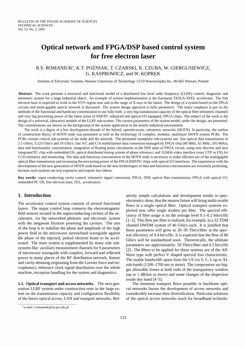
Fig. 1. Block diagram of the gigabit optical link (GOL) serialiser.CERN documentation (after Ref. 8–9)
Synchronisation is an important issue in HEP accelera-tors and FEL experiments, because it is absolutely vital forpreserving the integrity of the data and beam quality (elec-tron, hadron and photon). The commercial serdes componentsare in many cases the ideal choice. In some cases, a clockmanipulation is needed. For example the clock of the LHCaccelerator is 40.08 MHz, while some classical serdes chipsuse a reference clock of some multiple of 62.50 MHz. TheAgilent G-link HDMP-1022/24 chipset and its lower powersuccessors HDMP-1032A/34A have been more easily adapt-able in this respect but are less likely to become a widelyspread standard than Gigabit Ethernet. Recently several Gi-gabit Ethernet compatible serialisers with a wider range of op-erating frequencies have become available. The Gigabit Eth-ernet component that has raised the biggest interest in theHEP community is the Texas Instruments TLK2501. Sev-eral different groups have built link prototypes based on thiscomponent, or the Agilent G-link, and have reported verygood BER results of10−13 and∼ 80 ns latency. These twocomponents have also been tested for radiation tolerance bydifferent groups. The results are quite encouraging and in-dicate that both components can be used in the outer partsof the CMS experiment. The link latency is an issue ofparticular interest for the trigger links. The TLK2501 hasa smaller latency and a much shorter synchronization timethan the G-link, two frames of 25µs compared to 2 ms [8].
A gigabit serialiser ASIC with an integrated VCSEL drivercircuit has been developed at CERN to fulfill the specific re-quirements of the LHC experiments, Fig. 1 [8]. This com-ponent, called GOL (Gigabit Optical Link), is a good exam-ple of how a conventional 0.25µm CMOS process can beused to produce radiation tolerant devices using special lay-out practices and error mitigation techniques. The GOL hasa gate-all-around transistors and carefully placed guard ringsto fight the total dose effects. SEUs (Single Event Upsets)have been reduced by Hamming error detection and correc-tion for the configuration registers and by a triple modular re-dundancy design for the data path and control logic. Sincehard-wired pins are guaranteed to stay constant, all config-uration bits that are expected not to change during the op-
eration of the circuit are connected to external pins. TheMOS transistor widths have been increased for the serialiserand clock-generation circuits to increase the LET (LinearEnergy Transfer) that is required to cause upsets in them.
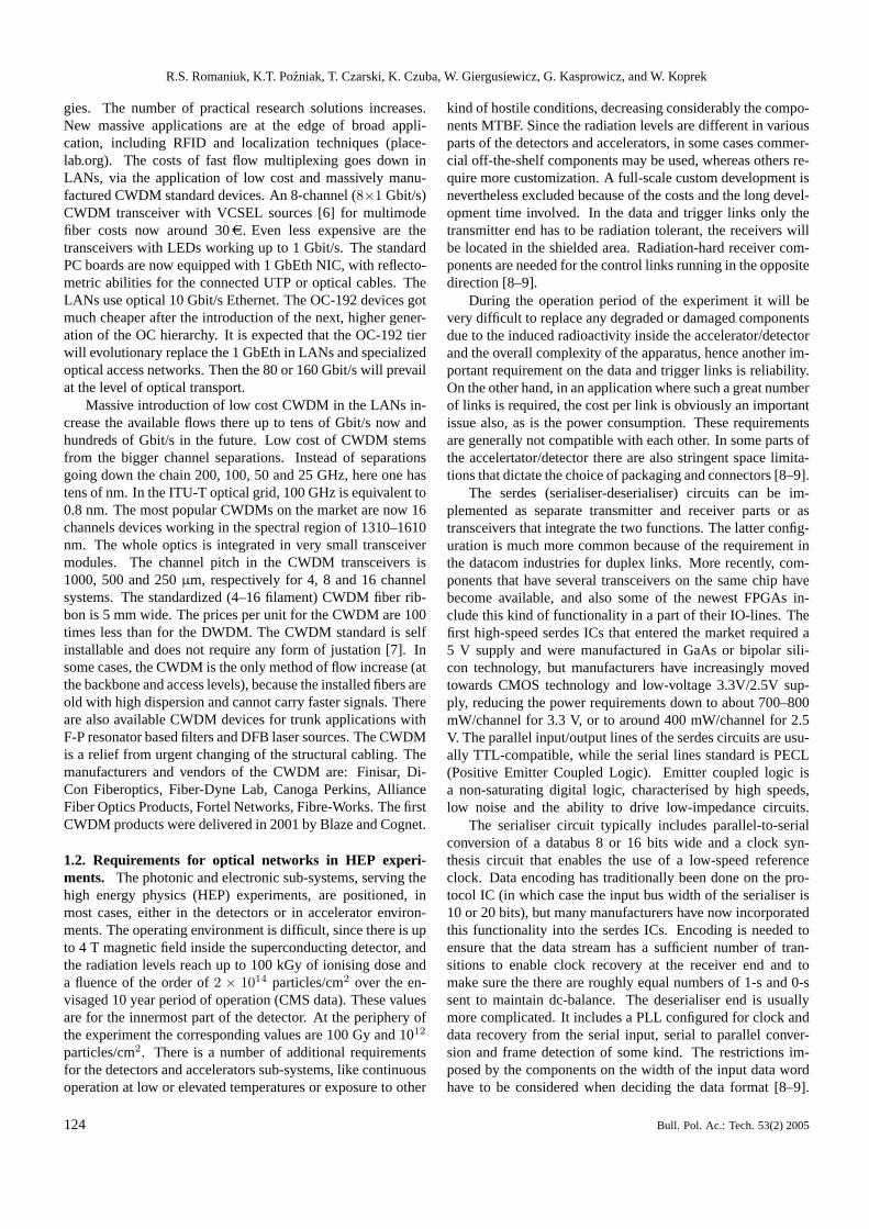
1.3. Accelerator control system.The TESLA–XFEL pro-ject bases on the nine-cell super conducting niobium res-onators to accelerate electrons and positrons. The accel-eration structure is operated in standingπ-mode wave atthe frequency of 1.3 GHz. The high power RF oscil-lating field is synchronized with the motion of a parti-cle moving at the velocity of light across the cavity [10].
The low level radio frequency control system (LLRF) [10-12] has been developed to stabilize the pulsed acceleratingfields of the resonators, Fig. 2. The control section, pow-ered by one klystron, may consist of many cavities. Oneklystron supplies the RF power to the cavities through the cou-pled wave-guide with a circulator. The fast amplitude andphase control of the cavity field is accomplished by modula-tion of the signal driving the klystron from the vector modula-tor. The cavities are driven with the pulses of 1.3 ms durationand the average accelerating gradients of 25 MV/m (up to 35MV/m). The RF signal of each cavity is down-converted to anintermediate frequency of 250 KHz (or recently 81 MHz) pre-serving the amplitude and phase information. The ADC andDAC converters link the analog and digital parts of the system.
A very dynamic development of the programmable FPGAcircuits, which has been observed during the last years, stimu-lated their wide applications the real-time LLRF systems [13–16]. The major driving factor behind the widening applica-tions is a considerable lowering of the chip costs relative tothe available number of the logical cells, the aggregated ca-pacity of the memory blocks and the aggregated processingpower of the inbuilt DSP components. This factor is con-stantly changing the FPGA circuits into the universal buildingblocks of any advanced photonic and electronic system design.The DSP equipped FPGA chips, when used in the LLRF sys-tem, make possible realization not only the basic functionaltasks but also for building of the whole new layers of diag-nostics and communications. The newest generations of theFPGA circuits promise even for more as they have integratedmodules of very fast communication interfaces with signalmultiplexing and demultiplexing in the direct I/O configura-tion. These I/Os may be either electrical (differential LVDS orPECL) or multi-gigabit optical [17]. The emerging standardsare Rocket I/O by Xilinx and SerialLight by Altera [18–19].
The paper debates the structural and functional modelof a universal, LLRF control system, for superconduct-ing accelerator, with integrated measurement and diagnos-tic functionalities, which bases on the FPGA chips of thenewest generation. The newest predicted features and de-velopment tendencies in the FPGAs were taken into ac-count. It was assumed that the system design shouldenable a relatively easy and low cost system modifica-tion (hardware upgrade, without physical exchange) forsome prolonged period of time after the commissioning.
Bull. Pol. Ac.: Tech. 53(2) 2005 125
R.S. Romaniuk, K.T. Pozniak, T. Czarski, K. Czuba, W. Giergusiewicz, G. Kasprowicz, and W. Koprek
Fig. 2. General functional block diagram of LLRF Multiple Cavity Control System
Here, the modification capability means the efficient adapta-tion to the changing and extending requirements of the (freeelectron laser, superconducting cavity) control process. Thesystem should also have the possibility to change the type ofthe FPGA chip, without rebuilding essentially the frameworkarchitecture. After some time of the development it is unavoid-able to change the system generation, but the parameterizationand inbuilt flexibility of the design avoids excessive costs ofthe prototyping process of the LLRF system.
2. Structural and functional model of LLRFsystem
The LLRF control system, for the superconducting niobiumcavity, may be considered, from the side of the data flow andprocessing, as a multichannel, synchronous, pipelined hard-ware concentrator, having the following features:
— Multichannel – The need to be multichannel is a fun-damental requirement, because the system is expectedto control independently up to several tens of cavities.The multi-parameter field control in the particular cavi-ties requires the presence of nondependent, synchronousreadout channels in the system. Some cavity parametersshould also be measured by the system to develop itscontrol potential and extend diagnostic capability. Thefeature of being multichannel enables building of mul-tilevel system. The channels are integrated in a vectorsum in the second tier of the system.
— Synchronous – This feature assures a simultaneous (andparallel, in a multichannel system) data processing forthe same moment of time, defined by the central systemclock of the accelerator. All the system events have to besituated extremely precisely in relation to the accelera-tor clock. The system time perturbations (jitters) have tobe taken into account. The perturbations may originate
from the signal jitter, dispersion and attenuation, differ-ences in the length of transmission lines causing differ-ential latencies, unexpected exceptional events, etc.
— Pipelined – This design approach stems from the com-plexity of the used system control procedures and algo-rithms. The signals are numerically processed in consec-utive steps. The data granularity is enabled for the sep-arate moments of time. The data can be distinguishedfor all channels, all moments of time and all stages ofthe signal processing in the LLRF control and measure-ment loop. The moments are determined by the centralsystem clock of the accelerator, powered by the masteroscillator.
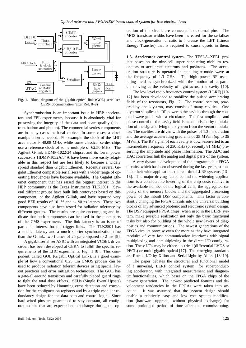
Fig. 3. A general functional structure of the data concentration pro-cess in the LLRF control system for superconducting cavity
126 Bull. Pol. Ac.: Tech. 53(2) 2005
Optical network and FPGA/DSP based control system for free electron laser
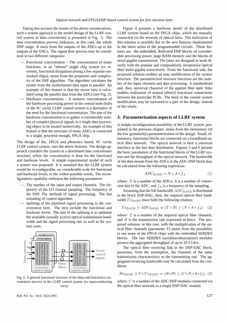
Taking into account the results of the above considerations,such a system approach to the model design of the LLRF con-trol system as data concentrator is presented in Fig. 3. Thedata concentration process embraces, in this case, the wholeDSP range. It starts from the outputs of the ADCs up to theoutputs of the DACs. The signal flow process may be consid-ered in two different categories:
— Functional concentration – The concentration of manyfunctions, in an “almost” single chip system (or re-versely, functional dissipation among a few separate net-worked chips), stems from the properties and complex-ity of the DSP algorithm. The algorithm calculates theresults from the multichannel data input in parallel. Anexample of this feature is that the vector sum is calcu-lated using the parallel data from the ADCs (see Fig. 2).
— Hardware concentration – A massive concentration ofthe hardware processing power in the central node (hub)of the SC cavity LLRF control system is a derivative ofthe need for the functional concentration. The aim of thehardware concentration is to gather a considerable num-ber of complex physical signals in a single data process-ing object to be treated numerically. An example of thisfeature is that the structure of many ADCs is connectedto a single, powerful enough, FPGA chip.
The design of the, FPGA and photonics based, SC cavityLLRF control system, uses the above features. The design ap-proach considers the system as a distributed data concentratorstructure, where the concentration is done for the functionaland hardware levels. A simple experimental model of sucha system was proposed. It is assumed that the LLRF systemwould be re-configurable, on considerable scale for functionaland hardware levels, in the widest possible extent. The recon-figuration capability embraces the following parameters:
— The number of the input and output channels. The fre-quency of the I/O channel sampling. The frequency ofthe DSP. The methods of signal processing. The fastreloading of control algorithm.
— Splitting of the pipelined signal processing to the con-centration tiers. The tiers include the functional andhardware levels. The aim of the splitting is to optimizethe available (usually scarce) optical transmission band-width and the signal processing rate as well as the sys-tem costs.
Fig. 4. A general functional structure of the (data and functions) con-centration process in the LLRF control system for superconducting
cavity
Figure 4 presents a hardware model of the distributedLLRF system based on the FPGA chips, which are mutuallyconnected via the network of optical links. The realization ofthis solution is possible due to the new features implementedin the latest series of the programmable circuits. These fea-tures are: the embedded, dedicated DSP blocks of consider-able processing power, large RAM memory and the blocks ofserial gigabit transmission. The latter are designed to work di-rectly with the popular and comparatively inexpensive opticalfiber multi-gigabit transceivers. From the functional side, theproposed solution enables an easy modification of the systemstructure. The parameterized structure functions are the num-ber of the input channels and data processing. A standardizedand, thus, universal character of the applied fiber optic linksenables realization of mutual (direct) functional connectionsbetween the particular PCBs. The need of the current systemmodification may be narrowed to a part of the design, insteadof the whole.
3. Parameterization aspects of LLRF system
A simple reconfiguration possibility of the LLRF system, pos-tulated in the previous chapter, stems from the elementary (ofthe low granularity) parameterization of the design. Small, el-ementary, functional blocks are connected via a broadband op-tical fiber network. The optical network is here a universalinterface to the fast data distribution. Figures 5 and 6 presentthe basic parameters of the functional blocks of the LLRF sys-tem and the throughput of the optical network. The bandwidthof the data stream from the ADCs in the ADC-DSP block maybe calculated from the following expression:
ADCBAND = N ∗A ∗ fA (1)
where:N is a number of the ADCs,A is a number of conver-sion bits of the ADC, andfA is a frequency of the sampling.
Assuming that the full bandwidthADCBAND is distributedto the block DSP-DAC, then, the required optical fiber band-width TxBAND must fulfil the following relation:
TxBAND ≥ ADCBAND ⇒ (T ∗B) ≥ (N ∗A ∗ fA) (2)
where: T is a number of the required optical fiber channels,andB is the transmission rate expressed in bits/s. The pro-posed solution, in this case, with the multiplication of the op-tical fiber channels (parameterT ) stems from the possibilityto use some of the FPGA chips with the embedded SERDESblocks. The fast SERDES (serializer/deserializer) modulespossess the aggregated throughput of up to 10.5 Gb/s.
The optical fibre receiving link in the DSP-DAC block,possesses, from the assumption, the channels of the sametransmission characteristics as the transmitting one. The ag-gregated receiving bandwidth may be calculated from the con-dition:
RxBAND ≥ C ∗TxBAND ⇒ (R∗B) ≥ (C ∗N ∗A∗fA) (3)
where:C is a number of the ADC-DSP modules connected viathe optical fiber network to a single DSP-DAC module.
Bull. Pol. Ac.: Tech. 53(2) 2005 127

R.S. Romaniuk, K.T. Pozniak, T. Czarski, K. Czuba, W. Giergusiewicz, G. Kasprowicz, and W. Koprek
Fig. 5. Parameterization of the ADC-DSP block
Fig. 6. Parameterization of the DSP-DAC block
The bandwidth of the output data stream from the D/A con-verters in the DSP- DAC block may be obtained from the rela-tion:
DACBAND = M ∗D ∗ fD) (4)
where:M is a number of D/A converters,D number of conver-sion bits of the converter,fD frequency of sampling. A con-clusion may be drawn from the above relations that the mostcritical components are:
— ADC channels concentration – in a single block, typi-cally situated on a single PCB. This is due to the tech-nological difficulties and the required aggregated band-width of fiber optic transmission.
— Multiplication of optical fiber links – in order to providethe required bandwidth of transmission. This forces the
use of a big number of the receivers in the DSP-DACmodule (parameter R).
4. Chosen function and data concentrationmethods for LLRF system
The functional and hardware concentration methods are ex-pected to minimize certain critical parameters of the LLRF sys-tem. This chapter discusses the four representative methods ofsuch methods, in order to obtain the optimal usage of the opti-cal fibre bandwidth and to optimize the implementations of thedata processing, control and diagnostics in the FPGA chips.The results were presented for certain work conditions of theLLRF systems of TESLA accelerator. The FPGA based (Xil-inx Virtex V3000) cavity controller was implemented earlier[13–14]. The initial system data are presented in Table 1.
Table 1System concentration parameters
Number of input channels (parameter N) ... 32Number of output channels (parameter M) ... 2Sampling frequency of ADC (parameterfA) ... 40 MHzSampling frequency DAC (parameterfD) ... 40 MHzFrequency of DSP process (parameterfS) ... 1 MHzWord width in DSP processing 18 bits
4.1. Data concentration from ADC. This kind of the con-centration process relies on the transmission, via optical links(to the DSP-DAC module) of the original data provided by all32 ADCs situated in the ADC-DSP module. It is the con-centration version imposing minimal functional requirementson the ADC-DSP module (no necessity to do any DSP opera-tion). In this modest case, the module may be equipped witha cheap and popular FPGA chip like Cyclone (by Altera) orSpartan (by Xilinx). As a consequence, the LLRF processingalgorithm modification in the DSP layer does not include theADC-DSP module. This solution requires a large optical trans-mission bandwidth. A detailed analysis result was gathered inTable 2 for the sampling frequencyfA = 40 MHz.
The results in the Table 2 show that, only in the case ofN = 8 andA = 8, the bandwidth of a single optical link issufficient to transmit all the data from the ADC-DSP module.In all other cases, the optical links multiplication is required,and the maximum value isT = 4. The main factor influenc-ing the bandwidth is the sampling frequency, which is herefA = 40 MHz. The next chapter presents a solution in whichthe required optical fiber link bandwidth may be considerablylowered.
Table 2Optical transmission bandwidth for chosen parameters of the LLRF system with the indirect concentration method
Number of ADC-DSP modules (parameterC) ADC channels (parameterN = 8) ADC channels (parameterN = 16)
Resolution of ADC (parameterA) 8 10 12 14 16 8 10 12 14 16
StandardSERDEStransmission(parameterB = 3.125 Gb/s)
ParameterTxBAND (Gb/s) 2.56 3.20 3.84 4.48 5.12 5.12 6.40 7.68 8.96 10.24ParameterT 1 2 2 2 2 2 3 3 3 4Bandwidth occupancy (%) 81.92 68.27 81.92 95.57 81.92 81.92 81.92 98.30 95.57 93.62ParameterRxBAND (Gb/s) 10.24 12.80 15.36 17.92 20.48 10.24 12.80 15.36 17.92 20.48ParameterR 4 8 8 8 8 4 6 6 6 8
128 Bull. Pol. Ac.: Tech. 53(2) 2005
Optical network and FPGA/DSP based control system for free electron laser
Table 3Optical transmission bandwidth for chosen parameters of the LLRF system in the concentration of modulated I/Q signalsd
Number of ADC-DSP modules (parameterC) ADC channels (parameterN = 8) ADC channels (parameterN = 16)
Resolution of ADC (parameterA) 8 10 12 14 16 8 10 12 14 16
StandardSERDEStransmission(parameterB = 3.125 Gb/s)
ParameterTxBAND (Gb/s) 0.06 0.08 0.10 0.11 0.13 0.13 0.16 0.19 0.22 0.26ParameterT 1 1 1 1 1 1 1 1 1 1Bandwidth occupancy (%) 2.05 2.56 3.07 3.58 4.10 4.10 5.12 6.14 7.17 8.19MaximumfS (MHz) 48.83 39.06 32.55 27.90 24.41 24.41 19.53 16.28 13.95 12.21ParameterRxBAND (Gb/s) 0.26 0.32 0.38 0.45 0.51 0.26 0.32 0.38 0.45 0.51ParameterR 4 4 4 4 4 2 2 2 2 2
4.2. Modulated signals concentration I/Q. The concentra-tion of the modulated I/Q signals in the ADC/DSP moduleenables reduction of the sampling frequency fromfA = 40MHz to fS = 1 MHz for each measurement channel. Inthis case, each channel has to possess the independent, pro-grammable correction components. The following parametersare subject to the correction: amplification changes, stabiliza-tion of the reference level, signal averaging block, low-passfiltering, etc. These solutions require the use of the faster andthe bigger FPGA circuits than in the previous case. The DSPblocks in these FPGAs are required too. This kind of process-ing serves only for conditioning of the measurement signal. Itdoes not embrace within its extent the LLRF control algorithm.This solution leads to the reduction of the required optical fiberbandwidth, what was presented in Table 3 for the sampling fre-quencyfS = 1 MHz.
The concentration of the modulated signals I/Q enablesnormalization (T = 1) of the number of optical fibre trans-mitters for the ADC-DSP modules and the number of opticalfiber receivers (R = C) in the DSP-DAC module, which is re-spective to the number of the transmitting modules. The band-width occupancy does not cross the value of 10%, which givesthe possibility to increase the I/Q signal modulation frequencyfrom the existing now 250 kHz even to 5 MHz without the ne-cessity to modify the structure of the optical fiber network. Theconsideration, in a further perspective, of much faster process-ing algorithms, involves the use of very advanced technologi-cally and large, thus expensive, FPGA chips. The next chapterspresent the solution embracing the process of concentration onthe level of the LLRF control algorithm. The tasks fulfilled ina single FPGA chip may be realized in a few smaller chips inthe fully distributed processing structure. The structure has anoptical network as a backbone.
4.3. I/Q signal concentration after detection. The concen-tration of the I/Q signals after detection in the ADC-DSP mod-ule enables performing of a part of the LLRF control algo-rithm on the level of the ADC-DSP block. The process stores,however, the overall control on each measurement channel inthe DSP-DAC module. The considered method of concen-tration requires the use of FPGA circuits equipped with theDSP blocks. The ADC-DSP block may realize a considerablepart of the diagnostics and monitoring of the particular chan-nels, apart form doing its regular task of functional processing.In this case, the costs of diagnostics and monitoring imple-mentation may be considerably distributed among a numberof FPGA chips. The required optical transmission bandwidthdepends on the width of the word used in the DSP algorithm.Table 4 presents the values of the required optical transmis-sion bandwidth for a few exemplary values of the width of DSword.
The method debated in this chapter does not allow for re-ducing the optical transmission bandwidth because the valuesof I and Q must be transmitted for all channels independently.The further possibility to reduce the transmission bandwidthmay be obtained by splitting the control algorithm, what is pre-sented in the next chapter.
4.4. Concentration of local vector sums.A much biggerfunctional concentration is obtained by performing the calcula-tions of the local vector sum already on the level of the ADC-DSP module. All the control, monitoring and diagnostics ofparticular channels have to be also implemented in the ADC-DSP module. A much bigger reduction of the optical band-width is obtained, because the vector sums are transferred. Thetransmission bandwidth depends on the width of the DSP wordwas presented in Table 5.
Table 4Optical fibre link transmission bandwidth for chosen parameters of the LLRF system in the concentration method for I and Q signals
Number of ADC-DSP modules (parameterC) ADC channels (parameterN = 8) ADC channels (parameterN = 16)
Width of DSP word (bits) 18 24 30 36 42 18 24 30 36 42
StandardSERDEStransmission(parameterB = 3.125 Gb/s)
ParameterTxBAND (Gb/s) 0.07 0.10 0.12 0.14 0.17 0.14 0.19 0.24 0.29 0.34ParameterT 1 1 1 1 1 1 1 1 1 1Bandwidth occupancy (%) 2.30 3.07 3.84 4.61 5.38 4.61 6.14 7.68 9.22 10.75MaximumfS (MHz) 21.70 16.28 13.02 10.85 9.30 10.85 8.14 6.51 5.43 4.65ParameterRxBAND (Gb/s) 0.29 0.38 0.48 0.58 0.67 0.29 0.38 0.48 0.58 0.67ParameterR 4 4 4 4 4 2 2 2 2 2
Bull. Pol. Ac.: Tech. 53(2) 2005 129
R.S. Romaniuk, K.T. Pozniak, T. Czarski, K. Czuba, W. Giergusiewicz, G. Kasprowicz, and W. Koprek
Table 5Optical transmission bandwidth for chosen parameters of LLRF system in the method of concentration of local vector sums
The width of DSP word (bits) 18 24 30 36 42
Standard SERDEStransmission (parameterB = 3.125 Gb/s)
ParameterTxBAND (Gb/s) 0.01 0.01 0.02 0.02 0.02Bandwidth occupancy (%) 2.29 0.38 0.48 0.58 0.67MaximumfS (MHz) 173.61 130.21 104.17 86.81 74.40ParameterRxBAND (Gb/s) 0.02 0.02 0.03 0.04 0.04
5. Universal model of distributed LLRF controlsystem
The realization of the eventual solution of the distributed LLRFcontrol system basing on the FPGA chips and optical fiber net-work will be preceded by the investigation of the laboratorymodel. The aim is to create the numerous structures of thesystem, and investigate the scalability, efficiency and reliabil-ity. The hardware and software layers are subject to practicalanalysis [15–16] for various models of concentration debatedin the previous section.
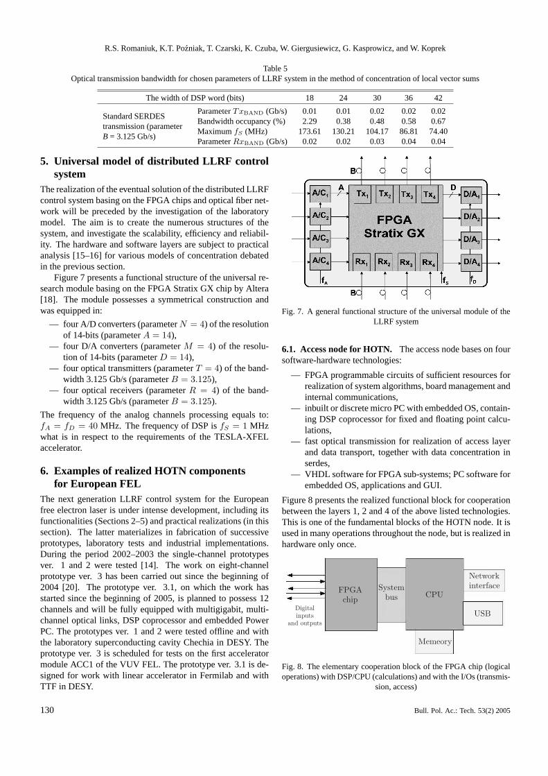
Figure 7 presents a functional structure of the universal re-search module basing on the FPGA Stratix GX chip by Altera[18]. The module possesses a symmetrical construction andwas equipped in:
— four A/D converters (parameterN = 4) of the resolutionof 14-bits (parameterA = 14),
— four D/A converters (parameterM = 4) of the resolu-tion of 14-bits (parameterD = 14),
— four optical transmitters (parameterT = 4) of the band-width 3.125 Gb/s (parameterB = 3.125),
— four optical receivers (parameterR = 4) of the band-width 3.125 Gb/s (parameterB = 3.125).
The frequency of the analog channels processing equals to:fA = fD = 40 MHz. The frequency of DSP isfS = 1 MHzwhat is in respect to the requirements of the TESLA-XFELaccelerator.
6. Examples of realized HOTN componentsfor European FEL
The next generation LLRF control system for the Europeanfree electron laser is under intense development, including itsfunctionalities (Sections 2–5) and practical realizations (in thissection). The latter materializes in fabrication of successiveprototypes, laboratory tests and industrial implementations.During the period 2002–2003 the single-channel prototypesver. 1 and 2 were tested [14]. The work on eight-channelprototype ver. 3 has been carried out since the beginning of2004 [20]. The prototype ver. 3.1, on which the work hasstarted since the beginning of 2005, is planned to possess 12channels and will be fully equipped with multigigabit, multi-channel optical links, DSP coprocessor and embedded PowerPC. The prototypes ver. 1 and 2 were tested offline and withthe laboratory superconducting cavity Chechia in DESY. Theprototype ver. 3 is scheduled for tests on the first acceleratormodule ACC1 of the VUV FEL. The prototype ver. 3.1 is de-signed for work with linear accelerator in Fermilab and withTTF in DESY.
Fig. 7. A general functional structure of the universal module of theLLRF system
6.1. Access node for HOTN. The access node bases on foursoftware-hardware technologies:
— FPGA programmable circuits of sufficient resources forrealization of system algorithms, board management andinternal communications,
— inbuilt or discrete micro PC with embedded OS, contain-ing DSP coprocessor for fixed and floating point calcu-lations,
— fast optical transmission for realization of access layerand data transport, together with data concentration inserdes,
— VHDL software for FPGA sub-systems; PC software forembedded OS, applications and GUI.
Figure 8 presents the realized functional block for cooperationbetween the layers 1, 2 and 4 of the above listed technologies.This is one of the fundamental blocks of the HOTN node. It isused in many operations throughout the node, but is realized inhardware only once.
Fig. 8. The elementary cooperation block of the FPGA chip (logicaloperations) with DSP/CPU (calculations) and with the I/Os (transmis-
sion, access)
130 Bull. Pol. Ac.: Tech. 53(2) 2005

Optical network and FPGA/DSP based control system for free electron laser
Table 6 presents exemplary data for the used FPGA chipsfrom two competing families Altera [18] and Xilinx [19]. Theavailable resources allow for realization of efficient networknode practically all inside the chip. In case of need the chipreaches for the available auxiliary external resources.
Table 6Resources of FPGA chips used for building the HOTN node
Internal resourcesAltera StratixGX
EP1SGX40GXilinx VirtexIIPro
XCE2VP100
LCELL 41.250 99.216Full-duplex gigabittransmission blocks
20(each 3.125 Gb/s)
20(each 3.125 Gb/s)
RAM memory 3.4 Mb 7.9 MbIntegrated DSP blocks 14 NoMultiplicationcircuits
112(each 9×9 bits)
444(each 18×18 bits)
Lock circuits 8 12I/O pins 548 1040
The access node was realized in parameterized form offunctional blocks. The blocks were described in VHDL. Theimplementation was loaded to the FPGA. The board is in theVME standard. The general structure of the board is presentedin Fig. 9, for the LLRF system of modular version.
The functional blocks process the data in parallel in the realtime. The core of the node are independent modules (may beseveral), which realize the main algorithm of the measurement-control loop. Here they are System Controller and SystemSimulator (SIMCON). These blocks reside in the FPGA chipand use inbuilt DSP blocks – fast multiplication circuits. Theblocks use data provided by the Programmable Data Con-troller. The preset parameters stem from the algorithms andare described in [10–12]. The module of Input Data Multi-plexer provides programmable choice of control signals for thefunctional blocks of the HOTN node. Internal, digital feedbackloops can be realized, connect external digital and analog sig-nals from the ADC converters or set test vectors programmedand stored in Data Acquisition Block.
The task of the Output Data Demultiplexer is the choice ofthe signals for DACs or signal registration in Data AcquisitionBlock. Appropriate configuration of the Input and Output Mul-
tiplexer enables analog feedback between functional modulesof the node. The block of Time and Status Controller providesinternal synchronization of the node processes. The choice be-tween the internal and external timing is possible, enablingthe autonomous work of the node and locally connected de-vices. The block of Communication Controller manages pro-gramming of all blocks from the managing computer system.There are used several I/O protocols for this purpose like EPP,RS, USB, JTAG. The block-hub architecture allows to extractcommon functionalities in different parts of the node. Thisleads to considerable simplification of the hardware modulesand software based control procedures. The design processembraces smaller number of completely different functionali-ties what lowers the costs and effort.
6.2. Architecture and parameters of PCBs for HOTN. Afew versions of the multi-gigabit access nodes to HOTN wererealized practically. The board for experimental modular ver-sion was presented in Fig. 10. This figure shows the frontand rear sides of this complex solution. It is the model of thebroadest hardware reconfiguration possibilities. The systemconsists of the backbone motherboard (BMB) capable of car-rying up to five mezzanine boards (DB). The small boards real-ize functional, measurement, communication and managementdevices. Each DB bases on its own FPGA chip. The BMBhardware platform was realized as 20 layers PCB in EURO-6HE standard using VME-BUS. Now, the following DBs areworking in the system:
— VME communication module, in slave work mode, us-ing FPGA Acex chip;
— Embedded PC module, equipped in ETRAX CPU(100MHz) and Acex chip,
— Gigabit Optical Transmission module (2.5 Gbit/s) de-signed to concentrate the data streams, possesses theFPGA Cyclone chip and two serdes chips TLK2501,
— Board controller, realized on Acex, provides the follow-ing functionalities: communications with standard exter-nal I/Os; internal communications with particular mod-ules; distribution of fast control and synchronization sig-nals for all modules and the system as a whole; The slotsA-D possess fast direct connections.
Fig. 9. Large amount of measurement data concentration in the HOTN node for control purposes. Block diagrams. Multi-board solution withoptical fibre network (left); single bard solution with the converters residing on the same board as FPGA chip (right)
Bull. Pol. Ac.: Tech. 53(2) 2005 131

R.S. Romaniuk, K.T. Pozniak, T. Czarski, K. Czuba, W. Giergusiewicz, G. Kasprowicz, and W. Koprek
Fig. 10. Backbone Motherboard construction for the modular board solution for the LLRF system
Fig. 11. Backbone Motherboard (BMB) with mezzanine boards, front side view and tests in the VME crate; the BMB is a platform for modularversion solution of the TESLA control system
132 Bull. Pol. Ac.: Tech. 53(2) 2005
Optical network and FPGA/DSP based control system for free electron laser
Fig. 12. Eight channel mezzanine bard for the central node of the HOTN (left) and BMB tested in 8-channel configuration in the VME carte(right)
— Common Power Supply module, provides all typicalvoltages to the slots, FPGA chips, buffers, convertersand analog components;
— Analog Data Concentrator module, with multichanneloptical data links, each 2.5 Gb/s for 16, 32 and moreanalog channels, serializers, user’s a ccess via VME orPC (Ethernet, EPP, USB), Stratix GX chip;
— Node Controller module in single channel solution ormultichannel solution, possessing VirtexII V4000 chipwith hardware DSP blocks, 8 AD channels and 4 DAchannels.
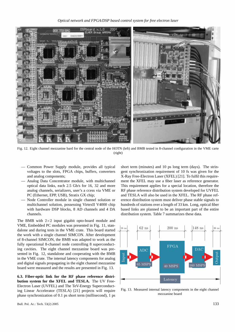
The BMB with 2×2 input gigabit opto-board module andVME, Embedded PC modules was presented in Fig. 11, stan-dalone and during tests in the VME crate. This board startedthe work with a single channel SIMCON. After developmentof 8-channel SIMCON, the BMB was adapted to work as thefully operational 8-channel node controlling 8 superconduct-ing cavities. The eight channel mezzanine board was pre-sented in Fig. 12, standalone and cooperating with the BMBin the VME crate. The internal latency components for analogand digital signals propagating in the eight channel mezzanineboard were measured and the results are presented in Fig. 13.
6.3. Fiber-optic link for the RF phase reference distri-bution system for the XFEL and TESLA. The UV Free-Electron Laser (UVFEL) and The TeV-Energy Superconduct-ing Linear Accelerator (TESLA) [21] projects will requirephase synchronization of 0.1 ps short term (millisecond), 1 ps
short term (minutes) and 10 ps long term (days). The strin-gent synchronization requirement of 10 fs was given for theX-Ray Free-Electron Laser (XFEL) [21]. To fulfil this require-ment the XFEL may use a fiber laser as reference generator.This requirement applies for a special location, therefore theRF phase reference distribution system developed for UVFELand TESLA will also be used in the XFEL. The RF phase ref-erence distribution system must deliver phase stable signals tohundreds of stations over a length of 33 km. Long, optical fiberbased links are planned to be an important part of the entiredistribution system. Table 7 summarizes these data.
Fig. 13. Measured internal latency components in the eight channelmezzanine board
Bull. Pol. Ac.: Tech. 53(2) 2005 133
R.S. Romaniuk, K.T. Pozniak, T. Czarski, K. Czuba, W. Giergusiewicz, G. Kasprowicz, and W. Koprek
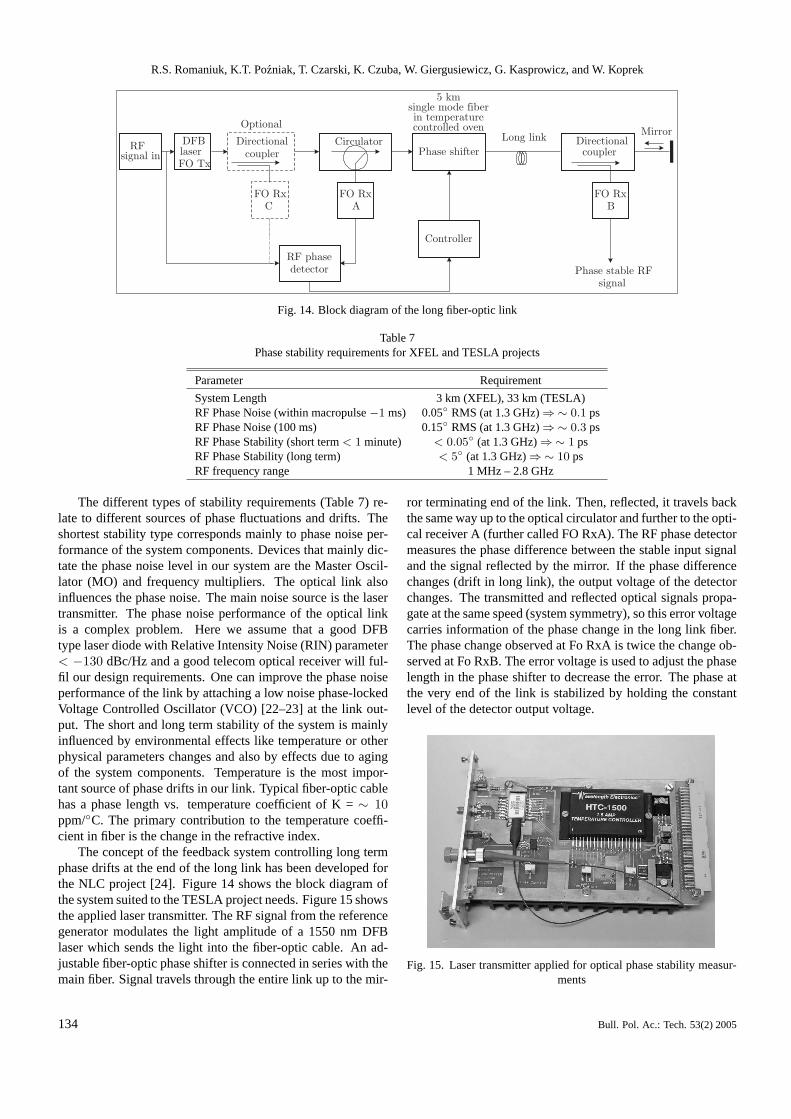
Fig. 14. Block diagram of the long fiber-optic link
Table 7Phase stability requirements for XFEL and TESLA projects
Parameter Requirement
System Length 3 km (XFEL), 33 km (TESLA)RF Phase Noise (within macropulse−1 ms) 0.05◦ RMS (at 1.3 GHz)⇒∼ 0.1 psRF Phase Noise (100 ms) 0.15◦ RMS (at 1.3 GHz)⇒∼ 0.3 psRF Phase Stability (short term< 1 minute) < 0.05◦ (at 1.3 GHz)⇒∼ 1 psRF Phase Stability (long term) < 5◦ (at 1.3 GHz)⇒∼ 10 psRF frequency range 1 MHz – 2.8 GHz
The different types of stability requirements (Table 7) re-late to different sources of phase fluctuations and drifts. Theshortest stability type corresponds mainly to phase noise per-formance of the system components. Devices that mainly dic-tate the phase noise level in our system are the Master Oscil-lator (MO) and frequency multipliers. The optical link alsoinfluences the phase noise. The main noise source is the lasertransmitter. The phase noise performance of the optical linkis a complex problem. Here we assume that a good DFBtype laser diode with Relative Intensity Noise (RIN) parameter< −130 dBc/Hz and a good telecom optical receiver will ful-fil our design requirements. One can improve the phase noiseperformance of the link by attaching a low noise phase-lockedVoltage Controlled Oscillator (VCO) [22–23] at the link out-put. The short and long term stability of the system is mainlyinfluenced by environmental effects like temperature or otherphysical parameters changes and also by effects due to agingof the system components. Temperature is the most impor-tant source of phase drifts in our link. Typical fiber-optic cablehas a phase length vs. temperature coefficient of K =∼ 10ppm/◦C. The primary contribution to the temperature coeffi-cient in fiber is the change in the refractive index.
The concept of the feedback system controlling long termphase drifts at the end of the long link has been developed forthe NLC project [24]. Figure 14 shows the block diagram ofthe system suited to the TESLA project needs. Figure 15 showsthe applied laser transmitter. The RF signal from the referencegenerator modulates the light amplitude of a 1550 nm DFBlaser which sends the light into the fiber-optic cable. An ad-justable fiber-optic phase shifter is connected in series with themain fiber. Signal travels through the entire link up to the mir-
ror terminating end of the link. Then, reflected, it travels backthe same way up to the optical circulator and further to the opti-cal receiver A (further called FO RxA). The RF phase detectormeasures the phase difference between the stable input signaland the signal reflected by the mirror. If the phase differencechanges (drift in long link), the output voltage of the detectorchanges. The transmitted and reflected optical signals propa-gate at the same speed (system symmetry), so this error voltagecarries information of the phase change in the long link fiber.The phase change observed at Fo RxA is twice the change ob-served at Fo RxB. The error voltage is used to adjust the phaselength in the phase shifter to decrease the error. The phase atthe very end of the link is stabilized by holding the constantlevel of the detector output voltage.
Fig. 15. Laser transmitter applied for optical phase stability measur-ments
134 Bull. Pol. Ac.: Tech. 53(2) 2005
Optical network and FPGA/DSP based control system for free electron laser
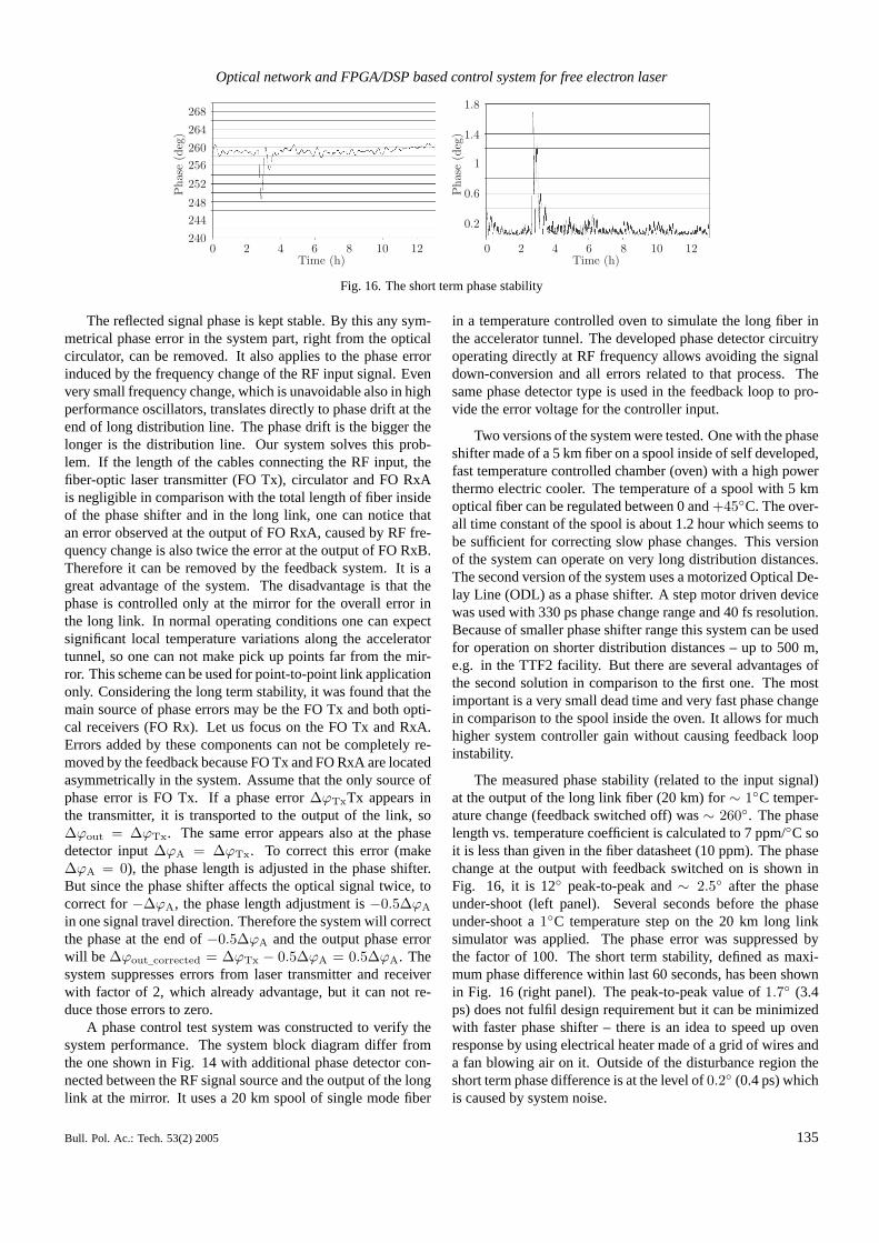
Fig. 16. The short term phase stability
The reflected signal phase is kept stable. By this any sym-metrical phase error in the system part, right from the opticalcirculator, can be removed. It also applies to the phase errorinduced by the frequency change of the RF input signal. Evenvery small frequency change, which is unavoidable also in highperformance oscillators, translates directly to phase drift at theend of long distribution line. The phase drift is the bigger thelonger is the distribution line. Our system solves this prob-lem. If the length of the cables connecting the RF input, thefiber-optic laser transmitter (FO Tx), circulator and FO RxAis negligible in comparison with the total length of fiber insideof the phase shifter and in the long link, one can notice thatan error observed at the output of FO RxA, caused by RF fre-quency change is also twice the error at the output of FO RxB.Therefore it can be removed by the feedback system. It is agreat advantage of the system. The disadvantage is that thephase is controlled only at the mirror for the overall error inthe long link. In normal operating conditions one can expectsignificant local temperature variations along the acceleratortunnel, so one can not make pick up points far from the mir-ror. This scheme can be used for point-to-point link applicationonly. Considering the long term stability, it was found that themain source of phase errors may be the FO Tx and both opti-cal receivers (FO Rx). Let us focus on the FO Tx and RxA.Errors added by these components can not be completely re-moved by the feedback because FO Tx and FO RxA are locatedasymmetrically in the system. Assume that the only source ofphase error is FO Tx. If a phase error∆ϕTxTx appears inthe transmitter, it is transported to the output of the link, so∆ϕout = ∆ϕTx. The same error appears also at the phasedetector input∆ϕA = ∆ϕTx. To correct this error (make∆ϕA = 0), the phase length is adjusted in the phase shifter.But since the phase shifter affects the optical signal twice, tocorrect for−∆ϕA, the phase length adjustment is−0.5∆ϕA
in one signal travel direction. Therefore the system will correctthe phase at the end of−0.5∆ϕA and the output phase errorwill be ∆ϕout_corrected = ∆ϕTx − 0.5∆ϕA = 0.5∆ϕA. Thesystem suppresses errors from laser transmitter and receiverwith factor of 2, which already advantage, but it can not re-duce those errors to zero.
A phase control test system was constructed to verify thesystem performance. The system block diagram differ fromthe one shown in Fig. 14 with additional phase detector con-nected between the RF signal source and the output of the longlink at the mirror. It uses a 20 km spool of single mode fiber
in a temperature controlled oven to simulate the long fiber inthe accelerator tunnel. The developed phase detector circuitryoperating directly at RF frequency allows avoiding the signaldown-conversion and all errors related to that process. Thesame phase detector type is used in the feedback loop to pro-vide the error voltage for the controller input.
Two versions of the system were tested. One with the phaseshifter made of a 5 km fiber on a spool inside of self developed,fast temperature controlled chamber (oven) with a high powerthermo electric cooler. The temperature of a spool with 5 kmoptical fiber can be regulated between 0 and+45◦C. The over-all time constant of the spool is about 1.2 hour which seems tobe sufficient for correcting slow phase changes. This versionof the system can operate on very long distribution distances.The second version of the system uses a motorized Optical De-lay Line (ODL) as a phase shifter. A step motor driven devicewas used with 330 ps phase change range and 40 fs resolution.Because of smaller phase shifter range this system can be usedfor operation on shorter distribution distances – up to 500 m,e.g. in the TTF2 facility. But there are several advantages ofthe second solution in comparison to the first one. The mostimportant is a very small dead time and very fast phase changein comparison to the spool inside the oven. It allows for muchhigher system controller gain without causing feedback loopinstability.
The measured phase stability (related to the input signal)at the output of the long link fiber (20 km) for∼ 1◦C temper-ature change (feedback switched off) was∼ 260◦. The phaselength vs. temperature coefficient is calculated to 7 ppm/◦C soit is less than given in the fiber datasheet (10 ppm). The phasechange at the output with feedback switched on is shown inFig. 16, it is 12◦ peak-to-peak and∼ 2.5◦ after the phaseunder-shoot (left panel). Several seconds before the phaseunder-shoot a1◦C temperature step on the 20 km long linksimulator was applied. The phase error was suppressed bythe factor of 100. The short term stability, defined as maxi-mum phase difference within last 60 seconds, has been shownin Fig. 16 (right panel). The peak-to-peak value of1.7◦ (3.4ps) does not fulfil design requirement but it can be minimizedwith faster phase shifter – there is an idea to speed up ovenresponse by using electrical heater made of a grid of wires anda fan blowing air on it. Outside of the disturbance region theshort term phase difference is at the level of0.2◦ (0.4 ps) whichis caused by system noise.
Bull. Pol. Ac.: Tech. 53(2) 2005 135

R.S. Romaniuk, K.T. Pozniak, T. Czarski, K. Czuba, W. Giergusiewicz, G. Kasprowicz, and W. Koprek
Fig. 17. Block diagram and PCB photograph of gigabit Ethernet interface for CCD camera (after Ref. 27)
The phase stability was also measured for the second ver-sion of the system – with motorized optical delay line. In thiscase a 5 km fiber spool inside the oven was used to simulate thelong link. A phase error of 300 ps was simulated (to be cov-ered by ODL range of 330 ps). Because of much faster phaseshifter, observed was no overshoot as in Fig. 16 and the longphase stability measured was equal0.4◦ (0.8 ps) peak-to-peak.The measurement duration was about 100 hours. In this casephase error was suppressed with a factor of 375 which is a verygood value. Obtained short term stability was also excellent –0.15◦ (0.3 ps) peak-to-peak. The result satisfies given stabilityrequirements.
In the future a series connection of phase shifter made ofspool inside the oven and ODL phase shifter is planned. Thissolution will utilize advantages of both devices. Coverage ofvery long distribution distance with feedback on phase will be
possible, as well as fast system response to operate with highcontroller gain and small output signal phase error.
6.4. Gigabit Ethernet interface. A realized gigabit Ethernetinterface for CCD camera is another example of functionalblock for HOTN access. The block diagram and the PCB lay-out of the interface are shown in Fig. 16. The applicationmay range from building a network of cameras, via monitoringthrough measurements. This particular interface was used forresearch in astronomy [25,26]. The (electrical or optical) Eth-ernet interface does not possess the confinements of the typi-cal USB solution. The TCP/IP connection makes out of thisdevice a powerful, standalone measurement unit. The unit, inseveral copies, was practically used in the globally networkedresearch of the optical flashes accompanying gamma ray burstsover the whole sky. The program “π of The Sky” is described
136 Bull. Pol. Ac.: Tech. 53(2) 2005
Optical network and FPGA/DSP based control system for free electron laser
elsewhere [25]. Eventually, the full research network will con-sist of 4 sets of 32 cameras each positioned in four places onthe Earth Globe to cover the whole sky.
In order to obtain the transmission rate of 40 ... 100 MB/s,the problem was a choice of proper MAC controller and thephysical layer of the link. The RTL9169S-32 controller (Real-tek) was chosen. Ti is a complete MAC circuit with integrated1000T physical layer. It possesses PCI interface running at 66MHz. It automatically calculates and verifies the control sumsfor the upper layers of the TCP/IP/UDP protocols. It resultsin lower demand for the processing power of the external pro-cessor. The automatic transfer and packet buffering from theexternal RAM, in BusMaster mode, speeds up the rate. How-ever the PCI interface has to be implemented in the FPGA. Theimplementation consists of the following blocks [27] (Fig. 17upper):
— PCI master block provides the communication betweenthe managing microcontroller and the interface. It real-izes transactions of the PCI bus: master read/write, con-figuration read/write. With the aid of this block, the pro-cessor initializes the interface, activates the PCI addressspace, Busmster mode and configures the register. ThePCI master block registers are mapped from the micro-processor side as the external data memory.
— Block PCI slave is a bridge between the PCI and thetransmitter and receiver buffers. The interface works inPCI SLAVE mode, during the data transmition from/tothe buffers. There were implemented two transmittingbuffers (each of them as 1 KB FIFO memory + head-ers) mapped in the address space of the PCI bus. TheFIFOs provide fast data transfer (over 200 MB/s). Thesememories are visible by the PCI interface as a continu-ous address space.
There is 128-byte buffer at the beginning of this address space.The µP places there the TCP/IP/UDP header. The next ad-dresses occupy the FIFO memory, where the right data are lo-cated. The SDRAM memory controller places the data there.There were implemented two full sets of the FIFO transmit-ter buffers, to improve the transfer efficiency. When the firstFIFO buffer is filled with data, the TCP/IP header is preparedand written to the second buffer. The MAC controller readsalternately buffers, checks and generates the control sums andsends data via the gigabit interface. This solution has verysmall demands for the processing power of theµP. Thus, 8-bitµP is fast enough to provide the implementation of the TCP/IPprotocol. The most time consuming part of the protocol (CRCcalculation) is realized in the hardware. Additionally, therewere implemented transmitter and receiver buffers to send sta-tus mode and commands.
The SDRAM memory controller, which serves the imagebuffer, has DMA circuit implemented to speed up the trans-fer between the buffer and FIFOs. Additionally, the SDRAMinterface may transmit data to the USB2 interface, which isperipherial circuit of 8051µC. The data are taken to the mem-ory directly from the ADC. The process is synchronized by theCCD sensor charge shift in the control circuit.
The main control block manages the Ethernet and USBtransmission. It provides synchronization of data transfer toFIFO buffers in the Ethernet and USB interfaces. The controlis done via the register file accessible as external memory oftheµP.
The PLL provides the clock signal of 48 MHz for theUSB interface, PCI board, DRAM memory and control logic.The interface was realized as a prototype PCI board, Fig. 17(lower). One PCI connector serves to communicate with giga-bit NIC the other is the edge one. The board features: powersupplies, FPGA Cyclone chip, DRAM memory, USB 2.0 inter-face chip and fast 210 MHz, 12bit ADC converter. The boardmay serve as a very fast frame grabber for analog signals, withPCI/USB interface, USB→ PCI bridge and may fulfill otherfunctions. The major aim is to provide the test environmentfor the GbEth board. In order to confine the amount of labourneeded to make the system work, the commercial GbEth PCIboard was used. Thus, the software implementation of the in-terface remained the major task.
The chip is controlled by the software executed on the Cy-pressµC FX2. It is the enhanced, fast 8051µP with integratedUSB 2.0 interface. It cooperates with the external program me-mory with serial I2C interface. The tasks of the software are:
— PCI board initialization, activation of the memory I/Oarea;
— board configuration, gigabit Ethernet interface initializa-tion, definition of descriptor addresses;
— preparation of packets to be sent, placing their addressesin the descriptor block, generation of the TCP/IP/UDPheader contents;
— decoding and executing incoming commands from bothinterfaces – Ethernet and USB. These orders may con-cern packets transmission synchronization, status of thedevice, starting of data acquisition, transmission or set-ting up parameters;
— reaction to errors caused by the PCI board, retransmis-sion of the lost packet;
— theµP serves also as controller and diagnostic device forthe whole measurement system cooperating with CCDcamera. These functions are: CCD matrix readout con-trol, shutter control, optical focus motor control, readoutfrom the temperature and humidity sensors, moisture,configuration of the video signal processor.
The interface was tested and a decision was taken to fabricatea number of copies. The camera with such interface is a pow-erful, standalone, measurement node of the broadband HOTN.
7. ConclusionsThe work presents a structural and functional model of a dis-tributed LLRF control system for the TESLA-XFEL accelera-tor. The model bases on FPGA circuits, (DSP and communi-cations functions equipped), and very fast, multigigabit, syn-chronous optical fiber data distribution system. The systemdesign enables uniquely its scaling and realization of variousmethods of data and processing power concentration on thefunctional and hardware levels.
Bull. Pol. Ac.: Tech. 53(2) 2005 137
R.S. Romaniuk, K.T. Pozniak, T. Czarski, K. Czuba, W. Giergusiewicz, G. Kasprowicz, and W. Koprek
The obtained functional solutions lower considerably therequired transmission bandwidth for the data. They providethe use of a single optical fiber channel, even at increasing theLLRF control algorithm frequency nearly 20 times. The im-plementation methods of the new LLRF control algorithm, ina distributed version, were described. This implementation re-sults practically in the possibility to distribute the system pro-cessing power into a few smaller FPGA chips.
The solutions, presented in this work, allowed preparinga universal model of the hardware module for the SC cavity,LLRF control system. The module enables building of a fullyscalable system structure in a broad range of technical func-tions and parameters. The debated functional and hardwareconcentration ideas were realized practically and are subject tofurther investigations of their practical performance. Some de-tails of technological solutions of HOTN subassemblies werepresented. There were given some examples of practical ap-plications of HOTN subsystems. The obtained design resultsand laboratory tests acknowledge that the application of theFPGA chips with optical transmission may redefine the role ofDSP chips for complex networked system algorithm realiza-tion. The new generations of programmable matrices possessdirect optical access to the pads. Now these are the followinginterfaces: Rocket I/O in the Virtex II and DirectLight in theStratix GX. The future will exchange these pins with directlyoptical pads to be connected with optical fibre.
The planned further development of the HOTN basedLLRF control system for TESLA embrace inclusion of : moremeasurement channels, localization of the measuring units(nodes) directly on the tube of the accelerating units, connect-ing the measuring nodes with fast fiber optic network, integra-tion of digital and analog subunits, dissipation of the systemintelligence, lowering the system cost, standardization of thesystem GUI and programming environment, etc.
The solutions presented in this work may find a varietyof applications beyond the original field they were designedfor. Acknowledgements. We acknowledge the support of theEuropean Community Research Infrastructure Activity underthe FP6 “Structuring the European Research Area” program(CARE, contract number RII3-CT-2003-506395).
REFERENCES
[1] R. Romaniuk,Optical Terabit Internet, KELTEL, PAN, War-saw, 2001, (in Polish).
[2] R.S. Romaniuk,DWDM, Technology, Measures, Exploitation,Development, Committee of Electronics and Telecommunica-tion PAN (KELTEL), PAS, Warsaw, 2001, (in Polish).
[3] R. Romaniuk, “Optical waveguides transmission with wavemultiplication – greater density or speed?”,ElectronicsXLV(5), 10–15 (2004), (in Polish).
[4] J. Wójcik, “Development of telecommunication waveguidetechnology in the beginning of XXI century”,Telecommunica-tion Review and Telecommunication News3, 135–143 (2002).
[5] K. Jedrzejewski, “Bragg’s nets – a new element in the telecom-munication optical waveguides”,Telecommunication Reviewand Telecommunication News3, 148–152 (2002), (in Polish).
[6] B. Mroziewicz, “Semiconductor lasers with tuned wavelength:perspectives of application in the optical networks”,Telecom-
munication Review and Telecommunication News3, 143–147(2002), (in Polish).
[7] Firm materials from internet: Finisar, DiCon, Fiberoptics,Fiber-Dyne, Canoga, AFO, Fortel, Fibre-Works, Optics.org,Fibers.org.
[8] K. Banzuzi and D. Ungaro, “Optical links in the CMS experi-ment”,Proc. SPIE5125, 101–111 (2003).
[9] K.T. Pozniak, M. Ptak, R.S. Romaniuk, K. Kierzkowski, I.M.Kudla, M. Pietrusinski, G. Wrochna, K. Banzuzi, and D. Un-garo, “Gigabit optical link test system for RPC muon trigger atCMS experiment”,Proc. SPIE5125, 155–164 (2003).
[10] T. Czarski, R.S. Romaniuk, K.T. Pozniak, and S. Simrock,“Cavity control system essential modeling for TESLA linearaccelerator”,TESLA Technical Note, DESY 06, (2003).
[11] T. Czarski, R.S. Romaniuk, K.T. Pozniak, and S. Simrock,“Cavity control system, models simulations for TESLA linearaccelerator”,TESLA Technical Note, DESY 08, (2003).
[12] T. Czarski, R.S. Romaniuk, K.T. Pozniak, and S. Simrock,“Cavity control system, advanced modeling and simulation forTESLA linear accelerator”,TESLA Technical Note, DESY 09,(2003).
[13] K.T. Pozniak, T. Czarski and R. Romaniuk, “Functional anal-ysis of DSP blocks in FPGA chips for application in TESLALLRF system”,TESLA Technical Note, DESY 29, (2003).
[14] K. T. Pozniak, T. Czarski, and R.S. Romaniuk, “FPGA basedcavity simulator and controller for TESLA test facility”,Proc.SPIE, 5775, 9–21 (2005).
[15] W. Koprek, P. Kaleta, J. Szewinski, K.T. Pozniak, T. Czarski,and R.S. Romaniuk, “Software layer for FPGA-based TESLAcavity control system”,Proc. SPIE5775, 32–43 (2005).
[16] P. Pucyk, T. Jezynski, W. Koprek, T. Czarski, K. Pozniak, andR. Romaniuk, “DOOCS server and client application conceptfor FPGA based cavity controller and simulator”,Proc. SPIE5775, 52–60 (2005).
[17] K.T. Pozniak, R.S. Romaniuk, T. Czarski, W. Giergusiewicz,W. Jalmuzna, K. Olowski, K. Perkuszewski, and J. Zielinski,“FPGA and optical network based LLRF distributed controlsystem for TESLA-XFEL linear accelerator”,TESLA Report09, (2004).
[18] http://www.altera.com/ [Altera Homepage][19] http://www.xilinx.com/ [Xilinx Homepage][20] W. Giergusiewicz, K. Kierzkowski, K.T. Pozniak, R.S. Roma-
niuk, “FPGA-based control module for x-ray fel and TESLAfeedback system”,Proc. SPIE5775, 61–68 (2005).
[21] http://tesla.desy.de [TESLA Home Page];http://tesla.desy.de/LLRF/ [LLRF home page];http://xfel.desy.de [XFEL Home Page]
[22] K. Czuba and H.C. Weddig, “Design considerations for theRF phase reference distribution system for X-Ray FEL andTESLA”, Proc. SPIE5484, 148–152 (2004).
[23] K. Czuba, F. Eints, M. Felber, and S. Simrock, “Fiber optic linkfor the RF phase distribution system for the XFEL and TESLAprojects”,Proc. SPIE5775, 44–51 (2005).
[24] J. Frish, D. G. Brown and E. L. Cisneros, “The RF phase distri-bution and timing system for the NLC”,XX International LinacConference, Monterey, California, pp. 745–747 (2000).
[25] http://grb.fuw.edu.pl/pi/ [“Pi-of-the-Sky” HomePage]
[26] A. Burd et al., “Pi of the Sky – all-sky, real-time search for fastoptical transients”,New Astronomy10 (5), 409–416 (2005).
[27] G. Kasprowicz, “Gigabit ethernet interface to CCD camera”,Internal Report PERG/ELHEP ISE PW01, (2005).
138 Bull. Pol. Ac.: Tech. 53(2) 2005