optical receivers theory and operation
DESCRIPTION
Optical Receivers Theory and Operation. Photodetector Requirements. High sensitivity ( responsivity ) at the desired wavelength and low responsivity elsewhere Low noise and reasonable cost Fast response time high bandwidth Insensitive to temperature variations - PowerPoint PPT PresentationTRANSCRIPT

Optical Receivers Theory and Operation

Photodetector Requirements
• High sensitivity (responsivity) at the desired wavelength and low responsivity elsewhere
• Low noise and reasonable cost
• Fast response time high bandwidth
• Insensitive to temperature variations
• Compatible physical dimensions
• Long operating life

Photodiodes• Due to above requirements, only photodiodes
are used as photo detectors in optical communication systems
• Positive-Intrinsic-Negative (pin) photodiode– No internal gain
• Avalanche Photo Diode (APD)– An internal gain of M due to self multiplication
• Photodiodes are reverse biased for normal operation

Basic pin photodiode circuit
• Incident photons trigger a photocurrent Ip in the external circuitry
Photocurrent Incident Optical Power

pin energy-band diagram
cg
hc
E Cut off wavelength depends on the
bandgap energy

Responsivity ()
Quantum Efficiency () = number of e-h pairs generated / number of incident photons
Avalanche PD’s have an internal gain M
0
/
/pI q
P h
0
pI q
P h
M
p
IM
I IM : average value of the total multiplied current
M = 1 for PIN diodes
mA/mW
APD PIN M

Responsivitycg
hc
E

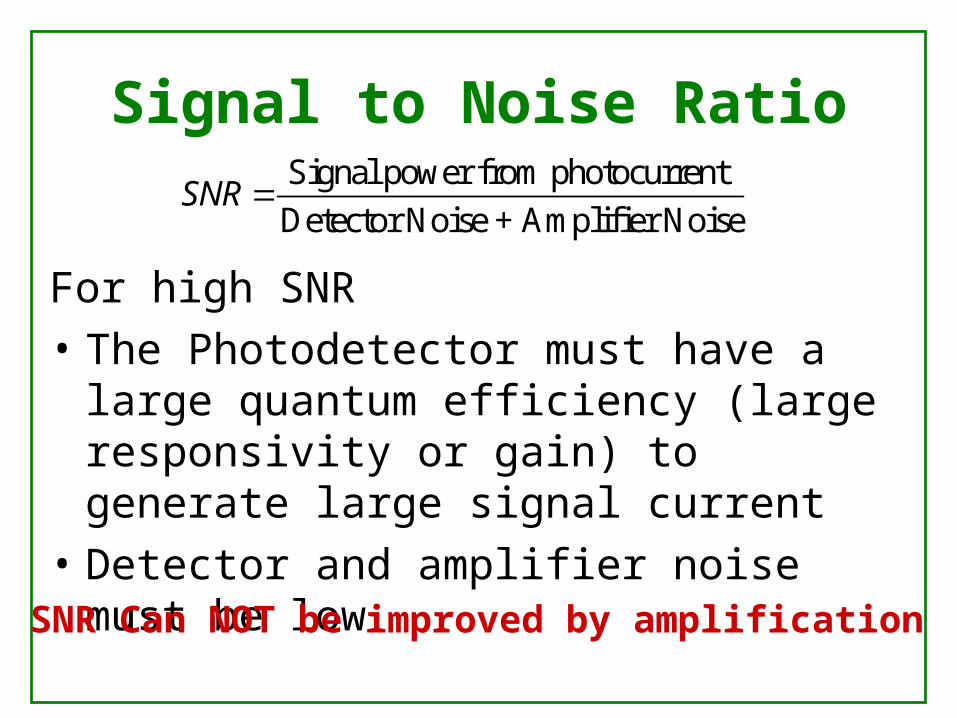
Signal to Noise Ratio
Signal to noise Ratio (SNR) as a function of the average number of photo electrons per receiver resolution time for a photo diode receiver at two different values of the circuit noise
Signal to noise Ratio (SNR) as a function of the average number of photoelectrons per receiver resolution time for a photo diode receiver and an APD receiver with mean gain G=100 and an excess noise factor F=2
At low photon fluxes the APD receiver has a better SNR. At high fluxes the photodiode receiver has lower noise
Signal to Noise Ratio
For high SNR
• The Photodetector must have a large quantum efficiency (large responsivity or gain) to generate large signal current
• Detector and amplifier noise must be low
Signal power from photocurrent
Detector Noise + Amplifier NoiseSNR
SNR Can NOT be improved by amplification

Quantum (Shot Noise)
)(2 22 MFBMqIi pQ
F(M): APD Noise Figure F(M) ~= Mx (0 ≤ x ≤ 1) Ip: Mean Detected CurrentB = Bandwidth
Due optical power fluctuation because light is made up of discrete number of photons
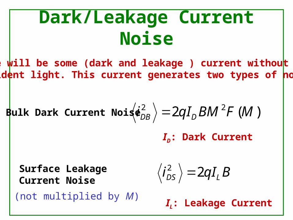
Dark/Leakage Current Noise
)(2 22 MFBMqIi DDB
BqIi LDS 22
Bulk Dark Current Noise
Surface Leakage Current Noise
ID: Dark Current
IL: Leakage Current
There will be some (dark and leakage ) current without any incident light. This current generates two types of noise
(not multiplied by M)

Thermal Noise
The photodetector load resistor RL contributes a mean-squarethermal (Johnson) noise current
LBT RTBKi /42
KB: Boltzmann’s constant = 1.38054 X 10(-23) J/K T is the absolute Temperature
• Quantum and Thermal are the important noise mechanisms in all optical receivers • RIN (Relative Intensity Noise) will also appear in analog links

Signal to Noise Ratio
2 2
22 ( ) ( ) 2 4 /p
p D L B L
i MSNR
q I I M F M B qI B k TB R
Detected current = AC component (ip) + DC component (Ip)
Signal Power = <ip2>M2
Typically not all the noise terms will have equal weight

SNRDark current and surface leakage current
noise are typically negligible, If thermal noise is also negligible
For analog links, (RIN= Relative Intensity Noise)
2
2 ( ) ( )p
p
iSNR
q I F M B
2 2
2 22 ( ) ( ) 4 / ( )
p
p D B L p
i MSNR
q I I M F M k T R RIN I B

Response Time in pin photodiode
Transit time, td and carrier drift velocity vd are related by
/d dt w v For a high speed Si PD, td = 0.1 ns

Rise and fall times
Photodiode has uneven rise and fall times depending on:1. Absorption coefficient s() and2. Junction Capacitance Cj
o rj
AC w

Junction Capacitance
o rj
AC w
εo = 8.8542 x 10(-12) F/m; free space permittivity εr = the semiconductor dielectric constant A = the diffusion layer (photo sensitive) areaw = width of the depletion layer
Large area photo detectors have large junction capacitance hence small bandwidth (low speed) A concern in free space optical receivers

Various pulse responses
( )0( ) (1 )s xP x P e
Absorbed optical power at distance x exponentially decaysdepending on s

Digital Receiver Performance
0 ( ) ( / 0)th
th VP V p y dy
1( ) ( /1)thV
thP V p y dy
11 02 ( ) ( )e th thP P V P V Probability of error assuming
Equal ones and zeros
Where,
Depends on the noise variance at on/off levels and the Threshold voltage Vth that is decided to minimize the Pe
Question: Do you think Vth = ½ [Von + Voff] ?

Logic 0 and 1 probability distributions
1( ) ( /1)thV
thP V p y dy
0 ( ) ( / 0)th
th VP V p y dy
1
1 02 ( ) ( )e th thP P V P V
Select Vth to minimize Pe
Asymmetric distributions

Noise variances
12( ) 1
2 2th
e on off
VP erf
Probability of error depends on Vth and noise power
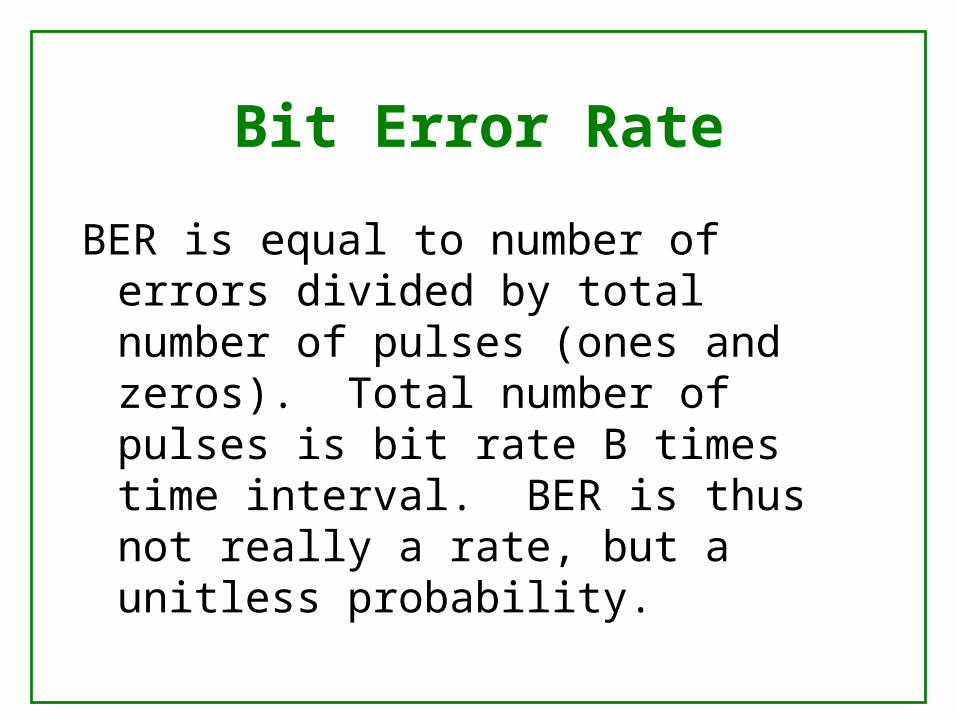
Bit Error Rate
BER is equal to number of errors divided by total number of pulses (ones and zeros). Total number of pulses is bit rate B times time interval. BER is thus not really a rate, but a unitless probability.

Q Factor and BER
on
thon
off
offth VVVVQ
21
2
1 QerfBER

BER vs. Q, continued
When off = on and Voff=0 so that Vth=V/2, then Q=V/2. In this case,
221
2
1
V
erfBER

Fig. 7-7: BER (Pe) versus
Q factor

BER vs SNR(equal standard deviations and boff = 0)

Sensitivity
The minimum optical power that still gives a bit error rate of 10-9 or below

Receiver Sensitivity
1/22
2 22
Sensitivity= Average detected optical power for a given bit error rate
For pin detectors
2 damplifier
hvP Q iq
i i qI I B
(Sm
ith a
nd P
erso
nick
198
2)
2 /2
-9
Probability of error vs. Q is to good approximation:
1 E 2
eg. for a SNR = Q = 6 Bit Error Rate= P(E)=10
QePQ