optimal ddr4 system with data bus inversion - xilinx · speaker hing yan (thomas) to technical...
TRANSCRIPT

TITLE
Image
Optimal DDR4 System with Data Bus Inversion
Hing Yan (Thomas) To, (Xilinx Inc.)
Changyi Su (Xilinx Inc.), Juan Wang (Xilinx Inc.)
Dmitry Klokotov (Xilinx Inc.), Lizhi Zhu (Xilinx Inc.), John Schmitz (Xilinx Inc.)
Penglin Niu (Xilinx Inc.), Yong Wang (Xilinx Inc.)
SPEAKERHing Yan (Thomas) To
Technical Director, Xilinx Inc.
Thomas is a Technical Director in System Memory Signal Integrity & Device Power Group at Xilinx, Inc. Prior to joining Xilinx, Thomas was with NVIDIA Advanced Technology Group focused on high speed (32GTs) circuits & system channel designs and supported different test chips for different advanced process nodes such as 20nm SOC & 16nm FINFET process. Before NVIDIA, Thomas worked for Intel for more than 16 years covered and led many different types of system memory IO development such as Sandy Bridge Server DDR IO and covered many different system memory technology ranging from DDR1 to DDR4. Thomas received his PhD degree in Electrical Engineering from the Ohio State University in 1995 & he has over 37 patents in the fields of mixed signal IO circuits and system memory configurations as well as high speed clocking for high speed memory designs.

Outline High Performance Computing Performance Requirement Trend
Typical Power Distribution in Computing System Example
System Memory Power Improvement Approach
Technology Process Node Scaling Trend
IO Voltage Scaling Trend
DDR4 IO signaling
Data Bus Inversion (DBI) in DDR4 Interface
DQ bus data Functional View with DBI enabled
DDR4 System Power Improvement Example
DDR4 IO Interface Training & Calibration with DBI
Power Noise Improvement with DBI
Experimental Data Margin Validation and Results
Summary & Conclusions
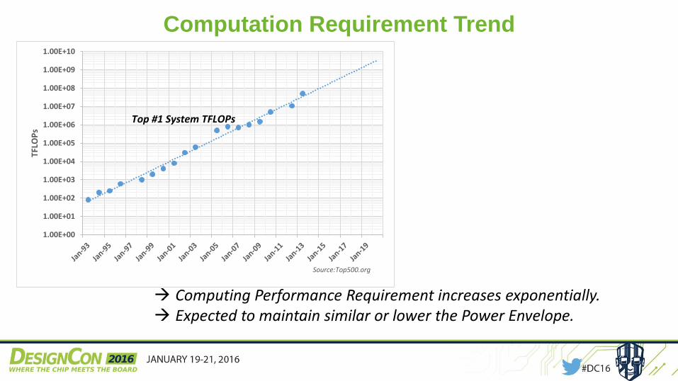
Computation Requirement Trend
1.00E+00
1.00E+01
1.00E+02
1.00E+03
1.00E+04
1.00E+05
1.00E+06
1.00E+07
1.00E+08
1.00E+09
1.00E+10
TFLO
Ps
Source:Top500.org
Top #1 System TFLOPs
Computing Performance Requirement increases exponentially. Expected to maintain similar or lower the Power Envelope.
Typical Power Distribution Comparison
60%14%
2%
19%5%
Xeon +DDR3CPU
Board
net
Mem
Store
30%
4%6%48%
12%
Atom + DDR3
CPU
Board
net
Mem
Store
Traditionally CPU has been the dominated component. System Memory becomes a factor as CPU power improves relatively.
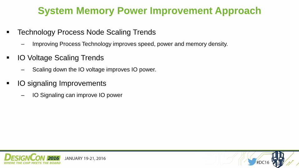
System Memory Power Improvement Approach
Technology Process Node Scaling Trends
– Improving Process Technology improves speed, power and memory density.
IO Voltage Scaling Trends
– Scaling down the IO voltage improves IO power.
IO signaling Improvements
– IO Signaling can improve IO power
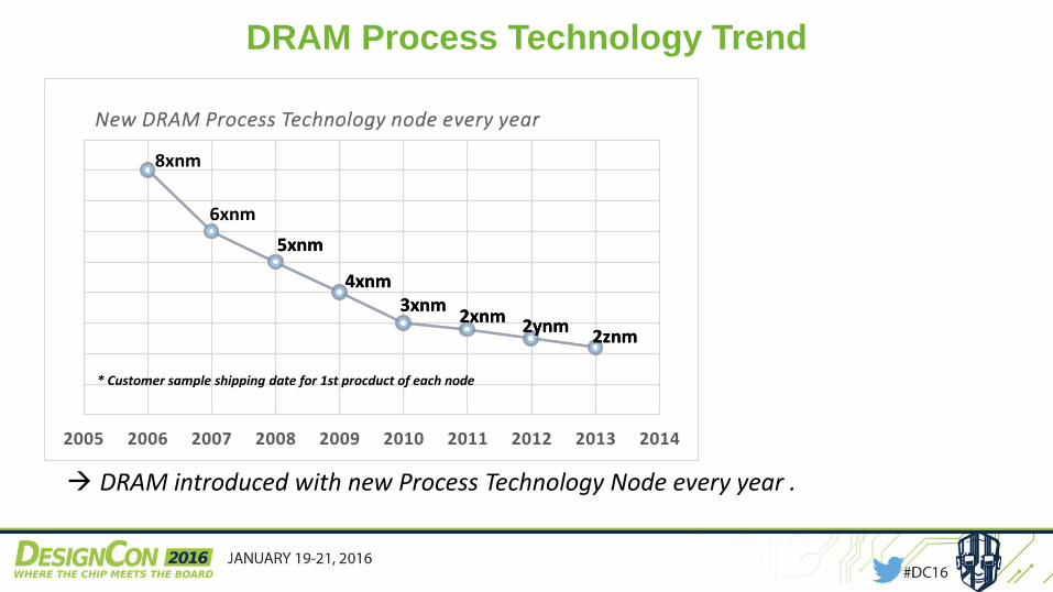
DRAM Process Technology Trend
2005 2006 2007 2008 2009 2010 2011 2012 2013 2014
New DRAM Process Technology node every year
5xnm
4xnm3xnm
2xnm2ynm
2znm
5xnm
4xnm3xnm
2xnm2ynm
2znm
* Customer sample shipping date for 1st procduct of each node
8xnm
6xnm
DRAM introduced with new Process Technology Node every year .
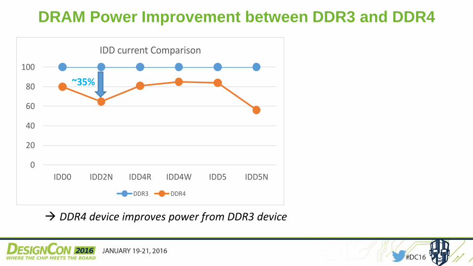
DRAM Power Improvement between DDR3 and DDR4
0
20
40
60
80
100
IDD0 IDD2N IDD4R IDD4W IDD5 IDD5N
IDD current Comparison
DDR3 DDR4
~35%
DDR4 device improves power from DDR3 device
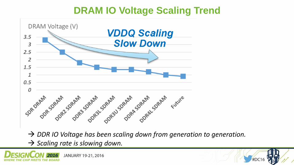
DRAM IO Voltage Scaling Trend
DDR IO Voltage has been scaling down from generation to generation. Scaling rate is slowing down.
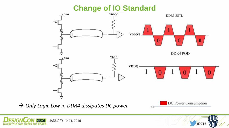
Change of IO StandardV D D Q
V D D Q
Only Logic Low in DDR4 dissipates DC power.

DDR4 Per Unit Power Distribution Comparison
17%
62%
21%
Relative Power Distribution
Total Activate Power
Total RD/WR/Term Power
Total Background Power
Even with Power Reduction w.r.t. DDR3, RD/WD/Term Power still a large portion. DDR4 can enable DBI to further improve IO power opportunistically.
Assume 70% Read/30%Write no DBI enabled

DBI Functional View
Data From Core
Controller with DBIEnabled capability
ChannelDRAM
DQ & DQS
DBI#

DBI Functional Burst Length View
Data From Core
Controller with DBIEnabled capability
ChannelDRAM
DQ & DQS
DBI#
Data FromCORE
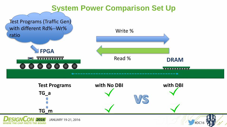
System Power Comparison Set Up
FPGA
DRAM
Write %
Read %
Test Programs (Traffic Gen) with different Rd%--Wr% ratio
Test Programs with No DBI with DBI
TG_a
TG_m
Read & Write Percentage Ratio for Relative Power
Comparison
79
77
75
73
70
67
63
50
57
44
40
21
23
25
28
30
33
37
50
43
56
60
TG_A(79%RD:21%WR)
TG_B(77%RD:23%WR)
TG_C(75%RD:25%WR)
TG_D(73%RD:28%WR)
TG_E(70%RD:30%WR)
TG_F(67%RD:33%WR)
TG_G(63%RD:37%WR)
TG_H(50%RD:50%WR)
TG_J(57%RD:43%WR)
TG_K(44%RD:56%WR)
TG_M(40%RD:60%WR)
Rd % Wr %
Analyze the relative power improvement with different work loads.
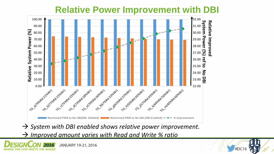
Relative Power Improvement with DBI
22.00
23.00
24.00
25.00
26.00
27.00
28.00
29.00
30.00
31.00
32.00
0.00
10.00
20.00
30.00
40.00
50.00
60.00
70.00
80.00
90.00
100.00
Nominized PWR to No DBI(DBI -Diabled) Nominized PWR to No DBI (DBI-Enabled) % Improvement
Rel
ativ
eSy
stem
Po
wer
(%
)
Relative Im
pro
vedSystem
Po
wer (%
) ref to N
o D
BI
System with DBI enabled shows relative power improvement. Improved amount varies with Read and Write % ratio
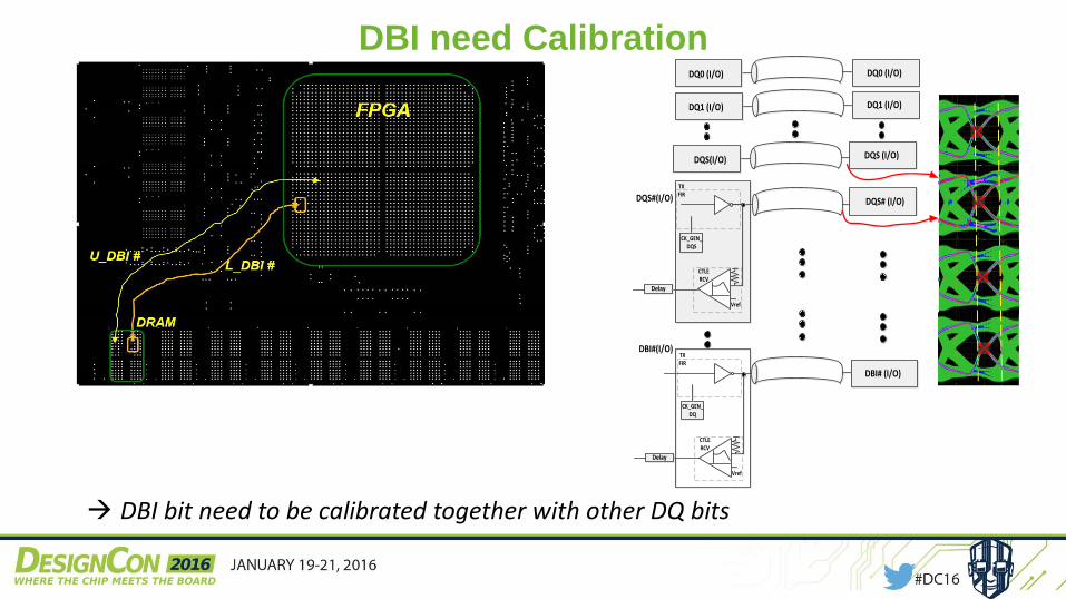
DBI need CalibrationDQ0 (I/O)
DQ1 (I/O)
DQS(I/O)
DQS#(I/O)
CK_GEN_DQ
TX FIR
DBI#(I/O)
DQ0 (I/O)
DQ1 (I/O)
DQS (I/O)
DQS# (I/O)
DBI# (I/O)
CTLE RCV
Vref
Delay
CK_GEN_DQS
TX FIR
CTLE RCV
Vref
Delay
DBI bit need to be calibrated together with other DQ bits

Step Function Representation of with DQ Pattern𝑫𝑸[𝟎] 𝒕 = 𝑫𝑸[𝟎]𝒓 𝒕 − 𝒓𝟏𝑻 − 𝑫𝑸[𝟎]𝒇 𝒕 − 𝒇𝟏𝑻 +⋯𝑫𝑸[𝟎] 𝒓 𝒕 − 𝒓𝒊𝑻 − 𝑫𝑸[𝟎]𝒇 𝒕 − 𝒇𝒊𝑻 +⋯
𝑫𝑸[𝟕] 𝒕 = 𝑫𝑸[𝟕]𝒓 𝒕 − 𝒓𝟏𝑻 − 𝑫𝑸[𝟕]𝒇 𝒕 − 𝒇𝟏𝑻 +⋯𝑫𝑸[𝟕] 𝒓 𝒕 − 𝒓𝒊𝑻 − 𝑫𝑸[𝟕]𝒇 𝒕 − 𝒇𝒊𝑻 +⋯
𝑫𝑸𝑺 𝒕 = 𝑫𝑸𝑺𝒓 𝒕 − 𝒓𝟏(𝑻 −𝑻
𝟐) − 𝑫𝑸𝑺𝒇 𝒕 − 𝒇𝟏 𝑻 −
𝑻
𝟐+⋯+𝑫𝑸𝑺𝒓 𝒕 − 𝒓𝒊(𝑻 −
𝑻
𝟐) − 𝑫𝑸𝑺𝒇 𝒕 − 𝒇𝒊(𝑻 −
𝑻
𝟐) + ⋯
Channel ConfigurationSystem

DQ Eye Reference to DQS𝐷𝑄_𝐷𝑄𝑆 𝐸𝑦𝑒(𝑡) = 𝑦(𝑡 + 𝑘𝑖𝑇) 0 ≤ 𝑡 ≤ 𝑇, ∀ 𝑘𝑖∈ ℕ0 , 𝑖 = 𝑟, 𝑓
TdivW_total
Vd
ivW
_to
talTjit
DV
Based on the rise and fall unit step response & their combinations:- Construct calibration pattern & to search for worst case jitter and eye height.
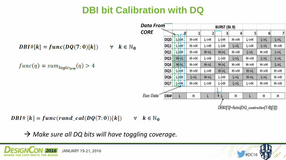
DBI bit Calibration with DQ
Make sure all DQ bits will have toggling coverage.
Data FromCORE
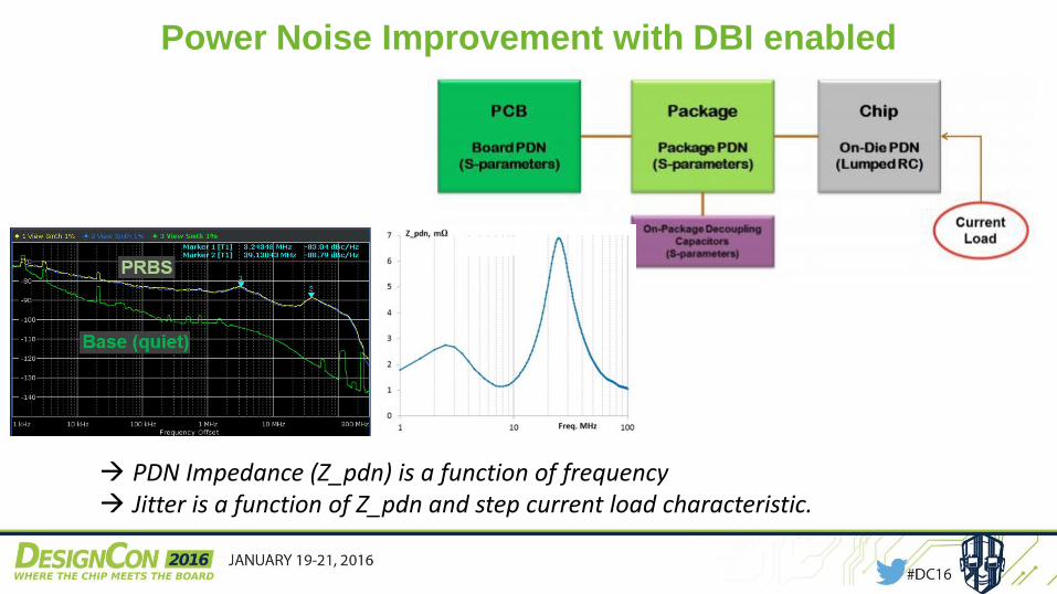
Power Noise Improvement with DBI enabled
PDN Impedance (Z_pdn) is a function of frequency Jitter is a function of Z_pdn and step current load characteristic.
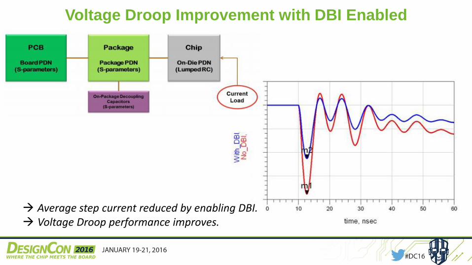
Voltage Droop Improvement with DBI Enabled
Average step current reduced by enabling DBI. Voltage Droop performance improves.
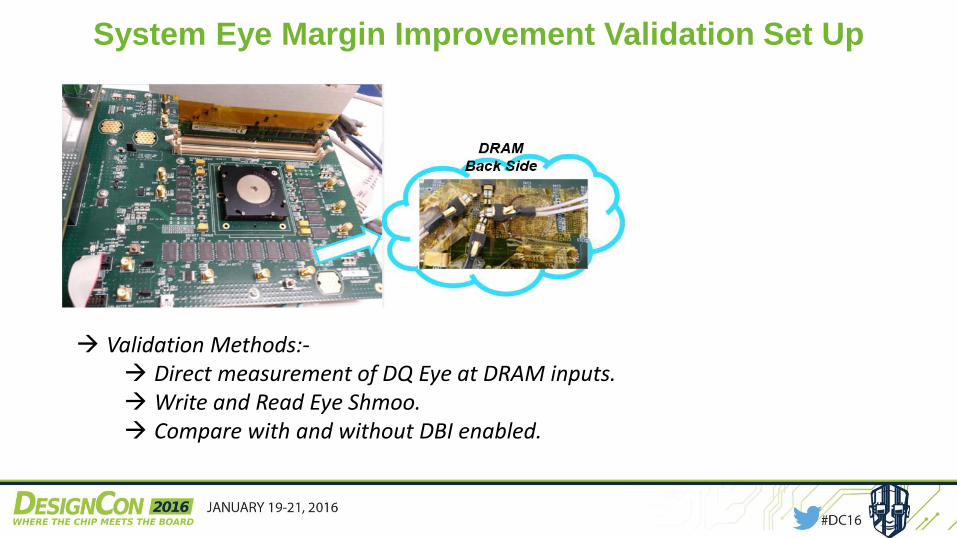
System Eye Margin Improvement Validation Set Up
Validation Methods:- Direct measurement of DQ Eye at DRAM inputs. Write and Read Eye Shmoo. Compare with and without DBI enabled.
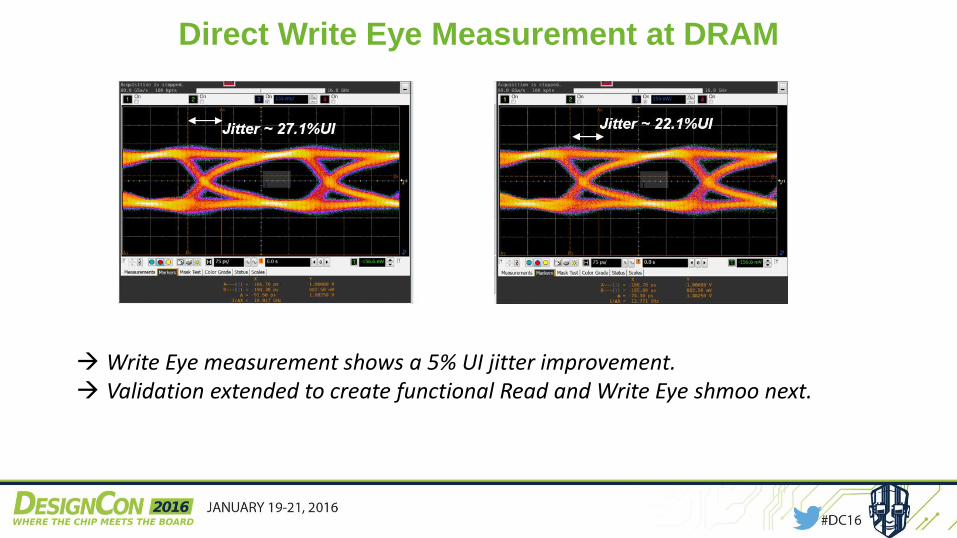
Direct Write Eye Measurement at DRAM
Write Eye measurement shows a 5% UI jitter improvement. Validation extended to create functional Read and Write Eye shmoo next.

Read and Write Shmoo Set Up
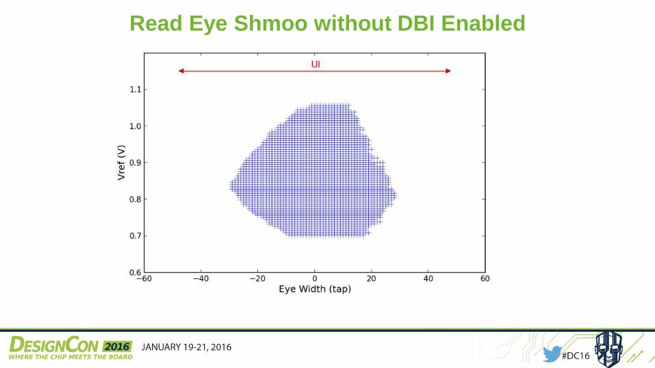
Read Eye Shmoo without DBI Enabled
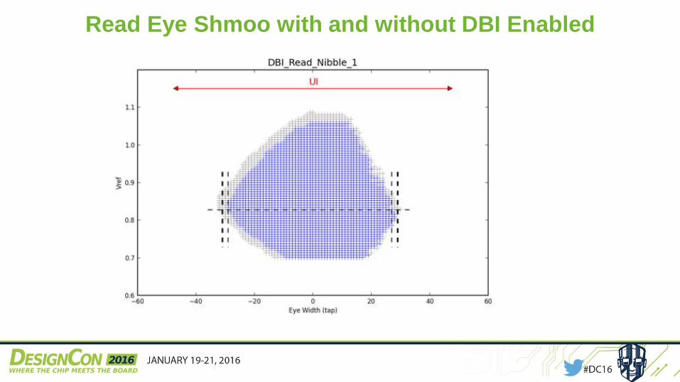
Read Eye Shmoo with and without DBI Enabled
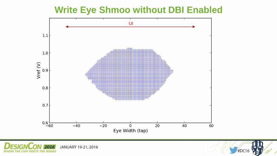
Write Eye Shmoo without DBI Enabled
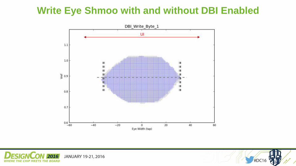
Write Eye Shmoo with and without DBI Enabled
94
96
98
100
102
104
106
108
110
112
Write Eye Width @ Vref Read Eye Width @ Vref
No DBI DBI
~11%
~7%
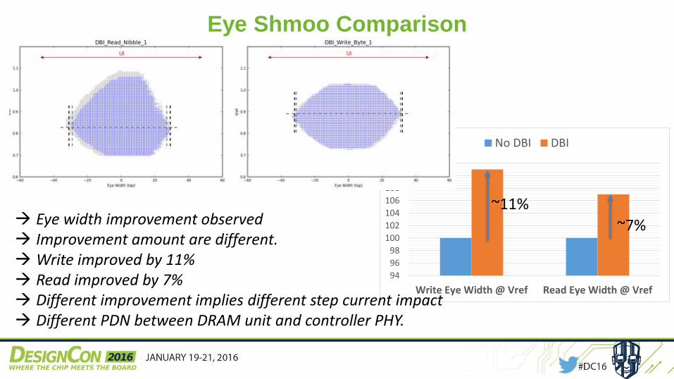
Eye Shmoo Comparison
Eye width improvement observed Improvement amount are different. Write improved by 11% Read improved by 7% Different improvement implies different step current impact Different PDN between DRAM unit and controller PHY.
Summary and Conclusions
Computing Performance requirements drive the need to reduce system power.
System memory Power became one of the major factor to the total system power.
Traditional improvement methods, such as scaling process node and IO voltage,
slow down.
DDR4 IO introduced DBI function to opportunistically reduce the IO power.
Power improvement amount varies with Write and Read Ratio.
DBI reduced the average step current in memory system, hence improved channel
margin.
Experimental data showed the Channel Jitter improvement differs between Write
and Read direction.

---
QUESTIONS?
Thank you!