optimization of printed tips-pentacene thin-film applied ... · lindo na cara um muito obrigado. ao...
TRANSCRIPT

Carla Sofia Gonçalves Martins
Licenciado em Ciências de Engenharia de Micro e Nanotecnologias
Optimization of Printed TIPS-PentaceneThin-Film Applied on OFET technology
Dissertation submitted in partial fulfillmentof the requirements for the degree of
Master of Science inMicro and Nanotechnologies Engineering
Adviser: Roberto Mendonça Faria, Full Professor,University of São Paulo
Co-adviser: Elvira Maria Correia Fortunato, Full Professor, NOVA Uni-versity of Lisbon
Examination Committee
Chairperson: Rodrigo Ferrão de Paiva MartinsRaporteurs: Luís Miguel Nunes Pereira
Members: Elvira Maria Correia Fortunato
DRAFT: January 2, 2017

Optimization of Printed TIPS-Pentacene Thin-FilmApplied onOFET technol-ogy
Copyright © Carla Sofia Gonçalves Martins, Faculdade de Ciências e Tecnologia, Univer-
sidade NOVA de Lisboa.
A Faculty of Sciences and Technology e a NOVA University of Lisbon têm o direito, per-
pétuo e sem limites geográficos, de arquivar e publicar esta dissertação através de exem-
plares impressos reproduzidos em papel ou de forma digital, ou por qualquer outro meio
conhecido ou que venha a ser inventado, e de a divulgar através de repositórios científicos
e de admitir a sua cópia e distribuição com objetivos educacionais ou de investigação, não
comerciais, desde que seja dado crédito ao autor e editor.
This document was created using the (pdf)LATEX processor, based in the “unlthesis” template[1], developed at the Dep. Informática of FCT-NOVA [2].[1] https://github.com/joaomlourenco/unlthesis [2] http://www.di.fct.unl.pt

Acknowledgements
Gostaria de começar por agradecer ao meu orientador, o Professor Dr. Roberto Faria, que
me recebeu e orientou na Universidade de São Paulo e cujo apoio, dedicação e entusiasmo
pela área fizeram toda a diferença ao longo dos vários momentos que constituíram esta
fase. Um grande obrigado por tudo do fundo do coração. À minha orientadora da FCT-
UNL, Prof. Dra. Elvira Fortunato, que me proporcionou a oportunidade de ir para a USP
realizar este trabalho e que cujo apoio em todo o processo foi indispensável.
Aos meus pais, Belém e Emília, a quem dedico esta tese, pelo apoio imprescindível em
todos os desafios a que me proponho. Devo a vocês a mulher que sou hoje. Ter conseguido
atingir esta meta teria sido impossível sem a vossa dedicação incansável ao longo dos meus
23 anos. As palavras faltam-me para agradecer tudo que me têm proporcionado.
Quero agradecer também aos meus irmãos, Joel e Henrique, por todas as brigas e
reconciliações, e por sempre me tratarem como uma eterna criança e assim me lembrarem
que sempre serei a menina dos vossos olhos.
Ao meu Dioguinho , o meu sobrinho afilhado preferido, por me encher de amor e de
mimo. Por me chamar de tia querida e me abraçar todas as vezes com tanta convicção e
carinho.
A toda a família do Prof. Faria em especial à Julia, a minha irmã de coração, por me
ter recebido de braços abertos no Brasil. Por todos os momentos incríveis passados em
São Paulo. Por todas as risadas e lágrimas, viagens e momentos de introspetiva, muito
obrigada super mulher.
A todas as pessoas do Grupo de Polímeros do Instituto de Física da USP que me aju-
daram na transição e me receberam como um deles em especial à Josiani pela orientação
com o equipamento Microdrop assim como com todo o procedimento realizado. Sem
você e o seu conhecimento não teria atingido os resultados obtidos. Obrigada Josi.
À Simone da secretaria do Grupo de Polímeros que sempre foi impecável quando
precisei de ajuda com qualquer assunto. Por todos os bom dias no grupo com um sorriso
lindo na cara um muito obrigado.
Ao Prof. Dr. Rodrigo Martins e à Prof. Dra. Elvira Fortunato pela criação, promoção
e reconhecimento alcançado pelo curso de Engenharia de Micro e Nanotecnologias.
À Moura, por todas as conversas, risadas, brigas, momentos partilhados ao longo de
todos estes anos, mas principalmente pela cumplicidade e amizade à distância que nunca
imaginei perdorar deste jeito um muito obrigada. Espero ter-te para sempre comigo.
Às minhas gatas de Barcelos, Mariana, Kika, Marta, Cláudia, Bea, Zé, Nokas e Driz por
todos estes anos de companheirismo, partilha, de risadas, parvoíces, mas principalmente
por sempre me apoiarem em todas as decisões que venho a tomar e sempre me receberem
de volta a casa de braços abertos com um sorriso na cara. Posso ir onde for, posso demorar
o tempo que demorar que sempre vos carrego comigo no coração. Todas as cidades do
mundo seriam fáceis de viver por tempo ilimitado se vos tivesse ao meu lado. Um livro
não chegava para explicar a importância destas mulheres na minha vida. Cada uma ao
seu jeito faz de mim uma pessoa melhor. Dos maiores orgulhos que tenho nesta vida é
poder chamar-vos de amigas. Obrigada por tudo manas pé na porta!
v

Ao meu Mano Cristiano por sempre me acompanhar nas aventuras, por ter sempre
uma palavra motivadora a dar, assim como por me fazer rir a toda a hora, um muito
obrigada!
Aos meus padrinhos da faculdade, Bea e Daniel, por me terem guiado desde o
primeiro dia da faculdade, por nunca me terem deixado sentir sozinha em Lisboa, por me
terem apoiado, aconselhado, rido e vivido toda a experiência que foi estudar na FCT ao
meu lado. Hoje ainda com mais certeza posso afirmar que escolhi os melhores padrinhos
do mundo. Muito obrigada!
Aos meus camaradas, companheiros de curso, Bártolo, Francisco, Correia, Luka, Trigo,
Monteiro e Tomás quero agradecer todas as experiências vividas e partilhadas ao longo
destes anos. Sei que poderei contar com vocês para sempre. Espero sempre ter este
grupinho por perto com a sua boa disposição para animar os meus dias.
À alfacinha da Joana Machado por todo o carinho e pela amizade tão bem regada ao
longo destes cinco anos. Espero sempre ter-te na minha vida, a aconselhar, acompanhar e
partilhar tudo que a vida terá para nos oferecer.
À Sabala por estar sempre lá quando eu preciso. Seja dia seja noite, faça chuva ou
faça sol sei que posso sempre contar contigo. Obrigada por todos os conselhos, risadas,
jantaradas e noitadas. Estás sempre lá, e sem muitos floreados, és a mana da margem sul
que todos precisavam de ter na vida. Obrigada chavala.
Aos meus afilhados, Alexandra, Cátia, Viorel, Fernandes, André, Miguel e Sérgio, com
especial atenção a este último caloirito que é muito mais que um afilhado, um grande
amigo que sempre esteve lá nos bons e maus momentos do meu mestrado, e que tenho
um orgulho enorme no homem com H grande em que se tornou.
Ao Zé, por todo o companheirismo ao longo destes cinco anos, pela partilha, pela
amizade, pela boa disposição, e noitadas. Este senhor sempre me ensinou e guiou ao
longo do meu percurso na Caparica e a ele devo grande parte do meu sucesso académico.
Um muito obrigada. Tenho muito orgulho em ter-te como amigo. Fico aqui para assitir
ao teu sucesso e aplaudir-te hoje e sempre.
Ao Jaime por todo o apoio incansável a toda a hora do dia e da noite e pelos abraços
apertados em horas de stress. É das pessoas que mais me surpreendeu ao longo do curso
e que mais falta me faz pela boa energia que sempre me fez sentir. Toda a gente precisa
dum Jaime como este nas suas vidas. Obrigada coração
À Fernanda e ao Carlos, por tudo que fizeram por mim no Brasil. Sem me conhecerem,
receberam-me em vossa casa em São Paulo sempre de bom grado e partilharam o vosso
espaço comigo. Vocês foram os Portugueses no Brasil que me apoiaram e me ajudaram
a matar as saudades do sotaque mais lindo de Portugal, o do Norte! Por todos os fins de
semana a passear por SP, pelas risadas, pela boa disposição e pelas loucuras, um muito
obrigada! Ficarão para sempre no meu coração e sempre terão a porta de minha casa
aberta.
À Naiara, a minha parceira da maldade de São Carlos um muito obrigada! Obrigada
por todas as risadas, cumplicidade, pelas loucuras, conversas pela noite dentro e por me
vi

teres recebido em tua casa de braços abertos de um jeito que eu nunca esquecerei. Espero
ver-te em breve amiga, fazes falta.
Ao Giácomo por seres a pessoa linda que és. Por todas as risadas, loucuras e brin-
cadeiras um muito obrigada. Em tão pouco tempo conseguis-te deixar marca na minha
vida, e entras-te no meu coração para ficar. O mundo precisa de mais homens como você.
Ao André, à Isabella, à Ana, às meninas da República Saia Jeans, à Bárbara, à Luciana,
aos meninos da Nossa Rep, e a todo o mundo de São Carlos, SP, que me recebeu e me
marcou um muito obrigada! Espero que a gente um dia se volte a encontrar.
Aos ex-basolhences, Jacinto, Diogo, Júlio, Rosado e Coelho, por todas as noitadas,
risadas partilhadas, por toda a vossa estupidez colectiva e principalmente pela vossa
amizade incondicional.
Ao Conselho de Praxe da FCT pela união, trabalho em equipa e companheirismo. A
praxe fez de mim uma pessoa melhor, devo a ela a maioria dos amigos que fiz na faculdade
e a vossas devo o reconhecimento por todo o amor e dedicação ao espírito académico.
Às minhas cadelas Lua, Mimi e à pequena Clarinha um muito obrigada. O amor que
elas me dão todos os dias faz de mim uma pessoa melhor.
A todas as pessoas do curso de MIEMN, aos que frequentam a 202 e a todos os que,
de alguma forma, contribuíram para que me tornasse na pessoa que sou hoje e que não
foram mencionadas em cima.
vii


"The distance between insanity and genius is measured only bysuccess."
Bruce Feirstein


Abstract
The area of Printed Electronics is relatively new, but promises to make a revolution
in several applications, particularly in smart cards and radio-frequency identification
devices (RFIDs). However, to achieve this goal is of fundamental importance to progress
towards printed transistors and complementary circuits. In this sense, this thesis aims
to advance the research on printing Organic Field-Effect Transistors (OFETs), both p-
type and n-type. The first step was to dominate the processing technique of thin films
composed by TIPS-Pentacene (a p-type molecule), as well as to adjust the parameters of
its solution to produce suitable electronic ink for inkjet printing. Other important step
was to treat the surface dielectric layer, which is as important as the semiconductor layer
for a good performance of an OFET. We choose poly(methyl metacrilate) (PMMA) as
the insulator material. A detailed study of the morphology of printed TIPS-Pentacene
was also carried out. After the deposition of the dielectric and the semiconductor layers,
which showed good crystallinity index, we characterized the p-OFET and built a pMOS
inverter, which shows to be promising in logical circuits. With these results in mind, the
next step is to build a CMOS inverter-TIPS Pentacene / P(NDI2OD-T2) and thus pave the
way for the manufacture of a complementary circuit.
Keywords: OFET, Inkjet, TIPS-Pentacene,Printed Electronics, SAM, HMDS
xi

Resumo
A área de Eletrónica Impressa é relativamente nova, mas promete revolucionar vários
setores sobretudo o de cartões inteligentes e de dispositivos de identificação por radio
frequência (RFIDs – Radio Frequency Identifications). No entanto, para tal é de funda-
mental importância o domínio da fabricação de transistores impressos e de circuitos com-
plementares. Neste sentido, esta tese tem como objetivo avançar nas pesquisas relativas
à impressão de transistores orgânicos por efeito de campo (OFETs – Organic Field-Effect
Transistors), tanto tipo p como tipo n. O primeiro passo foi dominar o processamento de
filmes finos compostos por TIPS-Pentaceno (molécula do tipo-p), assim como ajustar os
parâmetros da sua solução de modo a tornar-se numa tinta adequada à impressão pela
técnica Inkjet. Outro passo importante foi tratar a superfície da camada dielétrica, que
é tão importante quanto a camada semicondutora para o bom funcionamento de um
OFET. Usou-se o polimetracrilato de metila (PMMA) como material isolante. Um estudo
detalhado da morfologia do TIPS-Pentaceno impresso foi também realizado. Após a de-
posição do dielétrico e da camada semiconductora, que apresentou um bom índice de
cristalinidade , caracterizou-se o p-OFET e construiu-se um inversor pMOS, que demons-
tra ser um conceito promissor para os circuitos lógicos. Tendo em conta os resultados, o
próximo passo é construir um inversor CMOS TIPS-Pentacene/P(NDI2OD-T2) e assim
abrir caminho para a produção de circuitos complementares.
Palavras-chave: OFET, Inkjet, TIPS-Pentaceno, Eletrónica Impressa, SAM, HMDS
xiii


Contents
List of Figures xvii
List of Tables xix
Symbols xxi
Abreviations xxiii
Motivation xxv
1 Introduction 1
1.1 The Organic Field Effect Transistor (OFET) . . . . . . . . . . . . . . . . . . 1
1.1.1 Basic OFET Operation . . . . . . . . . . . . . . . . . . . . . . . . . 1
1.1.2 Carrier Transport Phenomenon . . . . . . . . . . . . . . . . . . . . 3
1.2 Inkjet Printing . . . . . . . . . . . . . . . . . . . . . . . . . . . . . . . . . . 4
1.2.1 Drying Process . . . . . . . . . . . . . . . . . . . . . . . . . . . . . 5
2 Materials 7
2.1 Organic Semiconductor-TIPS-Pentacene . . . . . . . . . . . . . . . . . . . 7
3 Experimental 9
3.1 Devices Fabrication . . . . . . . . . . . . . . . . . . . . . . . . . . . . . . . 9
3.2 Inkjet Printing Semiconductor Process . . . . . . . . . . . . . . . . . . . . 10
4 Analyse of the Dielectric and Active Layer 11
4.1 Device’s Architecture . . . . . . . . . . . . . . . . . . . . . . . . . . . . . . 11
4.2 Dielectric Layer . . . . . . . . . . . . . . . . . . . . . . . . . . . . . . . . . 11
4.2.1 Dielectric/semiconductor Interface Treatment . . . . . . . . . . . . 12
4.3 Semiconductor Layer . . . . . . . . . . . . . . . . . . . . . . . . . . . . . . 14
4.3.1 Semiconductor Solvent . . . . . . . . . . . . . . . . . . . . . . . . . 14
4.3.2 Printed Parameters for Semiconductor Layer . . . . . . . . . . . . 15
4.4 Structure and Morphology of the Printed Layers . . . . . . . . . . . . . . 17
4.4.1 Images of Scanning Electron Microscope . . . . . . . . . . . . . . . 17
4.4.2 Wide-Angle X-ray Diffraction . . . . . . . . . . . . . . . . . . . . . 18
5 OFETs and Inverter 21
5.0.1 OFETs: Drain current (ID ) versus source-drain voltage (VD ) . . . . 21
5.1 p-OFETs-tetralin . . . . . . . . . . . . . . . . . . . . . . . . . . . . . . . . . 22
5.2 Inverter Characterization . . . . . . . . . . . . . . . . . . . . . . . . . . . . 23
5.3 n-OFET . . . . . . . . . . . . . . . . . . . . . . . . . . . . . . . . . . . . . . 24
6 Conclusions and Final Remarks 27
Bibliography 29
xv

CONTENTS
A Electrical Characterization of OFETs 35
xvi
List of Figures
1.1 (a) Scheme of an OFET type Bottom Gate-Top Contact;(b) Correspondent elec-
tronic structure (adapted from [14]) . . . . . . . . . . . . . . . . . . . . . . . . 1
1.2 Operation regimes of Organic Field Effect Transistors (OFETs): (a) linear
regime; (b) pinch-off e (c) saturation regime. . . . . . . . . . . . . . . . . . . . 2
1.3 (a)Overlapping pz orbitals of the conjugated segment( Adapted from [23] );
(b) Illustration of bonding and antibonding interactions between HOMO and
LUMO levels . . . . . . . . . . . . . . . . . . . . . . . . . . . . . . . . . . . . . 4
1.4 Printable lines: (a) individual drops, (b) scalloped, (c) uniform, (d) with bumps
(bulges), and (e) stacked coins.(Adapted from [28]) . . . . . . . . . . . . . . . 5
1.5 Solvent evaporation during the drying process (Inspired by [29]) . . . . . . . 5
2.1 Molecular and stacking structure of pentacene (a and c) and of TIPS-Pentacene
(b and d, respectively). This figure has adapted from [30, 31] . . . . . . . . . 7
3.1 Schematic showing the process to obtain a OFET from a glass substrate previ-
ously clean (a), following to thermal evaporation of the gate (b), spin-coated
dielectric film (c) leading to its surface treatment with UVO Radiation (d) and
spontaneous evaporation of Self Assembled Monolayer (SAM) (e), deposition
of the TIPS-Pentacene by Inkjet Printer(f), and thermal evaporation of the
source and drain contacts (g) respectively. . . . . . . . . . . . . . . . . . . . . 9
3.2 shadow masks used for evaporation of the contacts source/drain (left) and
gate (right) . . . . . . . . . . . . . . . . . . . . . . . . . . . . . . . . . . . . . . 10
3.3 Printer Autodrop. Printer Overview (a) and expansion of the area highlighted
in green showing printing system (b) Drop Formation of the TIPS Pentacene
(c) . . . . . . . . . . . . . . . . . . . . . . . . . . . . . . . . . . . . . . . . . . . 10
4.1 Root-mean-square (RMS) roughness of PMMA (a) without treatment; (b) with
7s UVO treatment . . . . . . . . . . . . . . . . . . . . . . . . . . . . . . . . . . 13
4.2 The results of XRD spectroscopy of different TIPS-Pentacene solvents with (b
and d) and whithout (a and c) HMDS monolayer . . . . . . . . . . . . . . . . 14
4.3 Structural formula of: (a) tetralin, and (b) anisole . . . . . . . . . . . . . . . . 15
4.4 Printed TIPS-Pentacene/Anisole lines with different values of spacing drops 16
4.5 Coffee Ring Effect . . . . . . . . . . . . . . . . . . . . . . . . . . . . . . . . . . 16
4.6 Crystalline structures formed in printed (a) TIPS-Pentacene/Anisole lines to
250 µm spacing drops and (b) TIPS-Pentacene/Tetralin lines to 330 µm spac-
ing drops . . . . . . . . . . . . . . . . . . . . . . . . . . . . . . . . . . . . . . . 17
4.7 Analyzed SEM image and crystalization of an thin films formed by drop cast-
ing technique . . . . . . . . . . . . . . . . . . . . . . . . . . . . . . . . . . . . 18
4.8 Analyzed SEM image and crystalization of an thin films formed by inkjet
printing . . . . . . . . . . . . . . . . . . . . . . . . . . . . . . . . . . . . . . . . 18
4.9 WAXD obtained from: a) nude glass substrate; and b) the same substrate
coated with PMMA functionalized with HMDS. . . . . . . . . . . . . . . . . . 19
xvii

List of Figures
4.10 WADX obtained from TIPS-pentacene film deposited by: a)inkjet printing on
the substrate coated with PMMA functionalized with HMDS; b)drop casting 19
5.1 Drain current vs Drain-source voltage of p-OFETs: a) TIPS-pentacene dis-
solved in Anisole; b) TIPS-pentacene dissolved in Tetraline . . . . . . . . . . 21
5.2 Characteristic curves of a p-OFET printed at 36°C: (a) ID−VD curve; (b) ID−VGtransfer characteristic; and (c) (ID .L/W )2 x VG and Log(ID .L/W ) x VG curves. 22
5.3 Characteristic curves of a p-OFET printed at 46°C: (a) ID−VD curve; (b) ID−VGtransfer characteristic; and (c) (ID .L/W )2 x VG and Log(ID .L/W ) x VG curves. 23
5.4 PMOS inverter with a resistor load . . . . . . . . . . . . . . . . . . . . . . . . 23
5.5 Curves of voltage transfer characteristics of the digital inverter. (a) Effect of
resistance for VDD = 60V ; (b) Effect of variation of tension for R=300MΩ;
(c) Voltage Transfer Characteristic (VTC) curve with drive voltage gain for
VDD = 60V and R=300MΩ . . . . . . . . . . . . . . . . . . . . . . . . . . . . . 24
5.6 Molecular structure of P(NDI2OD-T2) . . . . . . . . . . . . . . . . . . . . . . 25
5.7 Characteristic curves of a n-OFET: (a) ID − VD curve; (b) ID − VG transfer
characteristic; and (c) (ID .L/W )2 x VG and Log(ID .L/W ) x VG curves.) . . . . . 25
A.1 Representative current-voltage characterisctics of an p-channel organic field-
effect transistor. (a) output characteristics;(b) transfer characteristics in the
linear regime indicating the onset voltage Von when drain current increases
suddenly; (c) transfer characteristics in the saturation regime indicating the
threshold voltage Vth. This figure has adapted of the [50] . . . . . . . . . . . 35
xviii

List of Tables
4.1 Parameters used to optimize the printing TIPS-Pentacene/Tetralin and TIPS-
Pentacene/Anisole . . . . . . . . . . . . . . . . . . . . . . . . . . . . . . . . . . 15
5.1 Parameters obtained for p-OFETs (TIPS-Pentacene with tetralin) heated at
36°C during the printing procedure. . . . . . . . . . . . . . . . . . . . . . . . 22
5.2 Parameters obtained for p-OFETs (TIPS-Pentacene with tetralin) heated at
46°C during the printing procedure. . . . . . . . . . . . . . . . . . . . . . . . 23
5.3 Truth Table . . . . . . . . . . . . . . . . . . . . . . . . . . . . . . . . . . . . . . 24
5.4 Parameters obtained for n-OFETs . . . . . . . . . . . . . . . . . . . . . . . . . 25
xix

Symbols
σ Conductivity
π π molecular orbital
ν Viscosity of the fluid
γ Surface tension
ρ Mass density
µOFET Charge carrier mobility
ID Drain current
ION /IOFF Current ratio
Oh Ohnesorge Number
VD Drain voltage
VG Gate voltage
Vth Threshold voltage
pz pz molecular orbital
sp2 sp2 atomic orbital
C Capacitance of dielectric
d Diameter of the drop
E Electric field
J Current density
L Lenght of the transistor
S Subthreshold swing
xxi

SYMBOLS
W Width of the transistor
xxii

Abreviations
BG/TC Bottom Gate/Top Contact
CIJ Continuous Inkjet Printing
CVD Chemical Vapor Deposition
DoD Drop on Demand
FET Field Effect Transistor
HMDS Hexamethyldisilazane
HOMO Highest Occupied Molecular Orbital
LUMO Lowest Unoccupied Molecular Orbital
nBA Butyl acrylate
OFET Organic Field Effect Transistor
OSC Organic Semiconductor
OTFT Organic Thin Film Transistor
PMMA Poly(methyl methacrylate)
PVP Poly(vinylpyrrolidinone)
RMS Root-mean-square
SAM Self Assembled Monolayer
SEM Scanning Electron Microscope
TIPS-Pentacene 6,13-Bis(triisopropylsilylethynyl)pentacene
UVO Ultraviolet Ozone
VTC Voltage Transfer Characteristic
WAXD Wide-Angle X-ray Diffraction
xxiii

ABREVIATIONS
XRD X Ray Diffraction
xxiv

Motivation
Organic semiconductor thin films have open a new branch in electronics that can be
named by “Wet Electronics”. This denomination, which sounds freak, defines precisely
the fact that organic electronics allows the manufacture of devices from an electronic
ink. This means that from an appropriate electronic ink it is possible to design and print
numerous electronic devices and circuits, by making use of several techniques that have
been developed recently. In our case an electronic ink is nothing more than a solution
of conjugated organic molecules in organic solvents. Important advantages are them de-
rived as their adaptability to low-temperature processing on flexible substrates, low cost
processing, amenability to high-speed fabrication, low consumption of inputs, and tun-
able electronic properties. Such features open possibilities for a variety of next-generation
electronic products, including circuits for smart cards, lowpower flexible displays, flexi-
ble radio frequency identification (RFID) tags, light panels, and printable sensors, among
many other applications [1–4]. The success of printed electronics depends on overcoming
the difficulties faced today in the control of printing techniques as well as in the creation
of new materials adequate to the preparation of electronic inks. In the specific case of
transistors, p-channel molecules are so far the leading class of organic semiconductors.
In contrast, n-type molecules are still relatively rare, but they are of great relevance for
the development of printed electronic devices such as OFETs. The scope of printed elec-
tronics includes a set of printing methods that has been developed to print electronic
and optoelectronic devices as well as circuitries on rigid and flexible substrates. The
most known techniques used for printed electronics are: screen printing, flexography,
rotogravure, offset lithography, and inkjet. Among them, one of the most suitable to print
devices in the micrometer scale is the Inkjet technique, mainly to print transistors and
complementary circuits [5, 6].
In this sense, this thesis intended to develop a work using inkjet printing to fabricate
organic field effect transistors (OFETs) with the objective to contribute to the printed
circuits area. We got this objective by the fabrication and characterization of p-OFETs
end with the first steps in the fabrication of n-OFETs.
xxv


Chapter 1
Introduction
1.1 The Organic Field Effect Transistor (OFET)OFETs, having a thin film as active layer, are particularly interesting mainly because
their fabrication processing are much less complex when compared with conventional Si
technology. While Si-technology involves high-temperature and high-vacuum deposition
processes associated with sophisticated photolithographic patterning methods, organic
electronics can be processed by easy deposition techniques using ordinary organic so-
lutions. In addition, the mechanical flexibility of organic thin films makes them natu-
rally compatible with plastic substrates for lightweight and foldable products. Although
OFETs are not meant to replace conventional inorganic transistors – because of the upper
limit of their switching speed – they have great potential for a wide variety of applications,
especially for new products that rely on their unique characteristics, such as electronic
newspapers, inexpensive smart tags for inventory control, and large-area flexible displays.
Since the coinage of the first OFET in 1986 [7], the performance of this type of device
has greatly progressed, as has been shown by several papers and reviews [8–15].Several
applications based on OFETs have been then created and refined, for example: in Light-
Emitting Field-Effect Transistor [16, 17], Flexible circuits [18], Optical displays [19], gas
sensors [20], and bioelectronics [21].
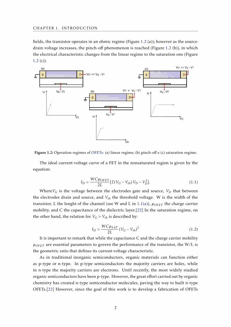
1.1.1 Basic OFET OperationOFETs exhibit a similar architecture to the Field Effect Transistors (FETs), i. e. they have
three electrodes (source, drain and gate), a semiconductor channel between the source
and the drain (which is isolated from the gate by a dielectric layer) as shown in the Figure
1.1(a). Figure 1.1(b) depicts the correspondent electronic structure of an OFET. The basic
principle of a FET consists of the modulation of the electric current flowing between the
source and the drain by the gate voltage.
(a) (b)
Figure 1.1: (a) Scheme of an OFET type Bottom Gate-Top Contact;(b) Correspondent electronicstructure (adapted from [14])
OFET operates in the accumulation mode, as shown in Figure 1.2 (a). At low electric
1
CHAPTER 1. INTRODUCTION
fields, the transistor operates in an ohmic regime (Figure 1.2 (a)); however as the source-
drain voltage increases, the pinch-off phenomenon is reached (Figure 1.2 (b)), in which
the electrical characteristic changes from the linear regime to the saturation one (Figure
1.2 (c)).
Figure 1.2: Operation regimes of OFETs: (a) linear regime; (b) pinch-off e (c) saturation regime.
The ideal current-voltage curve of a FET in the nonsaturated region is given by the
equation:
ID =WCµOFET
2L[2(VG −Vth)VD −V 2
D ]. (1.1)
WhereVG is the voltage between the electrodes gate and source, VD that between
the electrodes drain and source, and Vth the threshold voltage. W is the width of the
transistor, L the lenght of the channel (see W and L in 1.1(a)), µOFET the charge carrier
mobility, and C the capacitance of the dielectric layer.[22] In the saturation regime, on
the other hand, the relation for VG > Vth is described by:
ID =WCµSAT
2L(VG −Vth)2 (1.2)
It is important to remark that while the capacitance C and the charge carrier mobility
µOFET are essential parameters to govern the performance of the transistor, the W/L is
the geometric ratio that defines its current-voltage characteristic.
As in traditional inorganic semiconductors, organic materials can function either
as p-type or n-type. In p-type semiconductors the majority carriers are holes, while
in n-type the majority carriers are electrons. Until recently, the most widely studied
organic semiconductors have been p-type. However, the great effort carried out by organic
chemistry has created n-type semiconductor molecules, paving the way to built n-type
OFETs.[22] However, since the goal of this work is to develop a fabrication of OFETs
2

1.1. THE ORGANIC FIELD EFFECT TRANSISTOR (OFET)
making use of printing methods by specific technique known by Inkjet, we limit ourselves
to p-type transistors.
1.1.2 Carrier Transport PhenomenonAs already mentioned above OFETs are usually unipolar devices and operate in the ac-
cumulation regime, as shown in the sketches of Figure 1.2. It is important to note that
for a perfect operation, the source electrode has to be a blocking contact while the drain
electrode should collect the incoming charge carriers without any obstacle. In the linear
regime, along the channel, the Ohm’s law is obeyed, i. e.,
J = Eσ (1.3)
where J is the current density, σ the conductivity and E the electric field established
between the source and drain electrodes. It is important to emphasize that the electric
field, even for the highest used voltages, does not exceed the value of 100 KV/cm, which
discards any effect of the field on the channel conductivity. In order to reach such value
the channel length would have a length below 1 µm. On the other hand, the channel
conductivity depends on the chemical features of the organic molecule and on the mor-
phological structure of the thin film.
Organic Semiconductors (OSCs) are carbon-based compounds that exhibit a special
configuration from which semiconducting properties are derived. Their backbone is
based on carbon-hydrogen and invariably presents an alternate sequence of single and
double bonds. The semiconductor properties are possible because carbon atoms can
form three sp2 hybridized orbitals (one the molecular plan) and one unhybridized orbital,
which is commonly denoted as pz orbital (one the perpendicular plane to the sp2 orbitals).
This type of hybridization allows the formation of three high energy σ bonds (one per
each hybridized orbital) and two π bonds of low energy (one π bond and one antibond
π*). This orbital configuration creates a large energy difference between the occupied
bond π or the Highest Occupied Molecular Orbital (HOMO), and the unoccupied bond
π* or the Lowest Unoccupied Molecular Orbital (LUMO) (Figure 1.3(b)). Unhybridized
orbitals pz provide electron clouds above and below the molecular plain. The adjacent pzorbitals overlap resulting in shared molecular orbitals that are often referred as extended
π-system (see Figure 1.3(a)). Electrons on these orbitals are spatially delocalized, meaning
that they belong to the whole π-system, but not to specific carbon atoms. A π- system can
be extended over the entire organic molecule or just over a conjugated segment. [23–25]
3
CHAPTER 1. INTRODUCTION
(a) (b)
Figure 1.3: (a)Overlapping pz orbitals of the conjugated segment( Adapted from [23] ); (b) Illus-tration of bonding and antibonding interactions between HOMO and LUMO levels
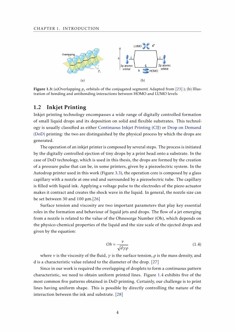
1.2 Inkjet PrintingInkjet printing technology encompasses a wide range of digitally controlled formation
of small liquid drops and its deposition on solid and flexible substrates. This technol-
ogy is usually classified as either Continuous Inkjet Printing (CIJ) or Drop on Demand
(DoD) printing: the two are distinguished by the physical process by which the drops are
generated.
The operation of an inkjet printer is composed by several steps. The process is initiated
by the digitally controlled ejection of tiny drops by a print head onto a substrate. In the
case of DoD technology, which is used in this thesis, the drops are formed by the creation
of a pressure pulse that can be, in some printers, given by a piezoelectric system. In the
Autodrop printer used in this work (Figure 3.3), the operation core is composed by a glass
capillary with a nozzle at one end and surrounded by a piezoelectric tube. The capillary
is filled with liquid ink. Applying a voltage pulse to the electrodes of the piezo actuator
makes it contract and creates the shock wave in the liquid. In general, the nozzle size can
be set between 30 and 100 µm.[26]
Surface tension and viscosity are two important parameters that play key essential
roles in the formation and behaviour of liquid jets and drops. The flow of a jet emerging
from a nozzle is related to the value of the Ohnesorge Number (Oh), which depends on
the physico-chemical properties of the liquid and the size scale of the ejected drops and
given by the equation:
Oh =ν√dγρ
(1.4)
where ν is the viscosity of the fluid, γ is the surface tension, ρ is the mass density, and
d is a characteristic value related to the diameter of the drop. [27]
Since in our work is required the overlapping of droplets to form a continuous pattern
characteristic, we need to obtain uniform printed lines. Figure 1.4 exhibits five of the
most common five patterns obtained in DoD printing. Certainly, our challenge is to print
lines having uniform shape. This is possible by directly controlling the nature of the
interaction between the ink and substrate. [28]
4

1.2. INKJET PRINTING
Figure 1.4: Printable lines: (a) individual drops, (b) scalloped, (c) uniform, (d) with bumps(bulges), and (e) stacked coins.(Adapted from [28])
1.2.1 Drying ProcessCarrier transport in organic electronic devices is tightly related to the morphology of thin
films, which are the active layer of the most part of such devices. Thereby, crystalline
microstructures embedded in disordered structures determine the electric properties and
therefore the devices performance. Similar situation is faced by printed circuits, in which
the final structure of the printed thin film is established by interactions between the
organic molecules with the substrate and also depends on the evaporation rate of the
solvent. Therefore, the substrate surface energy and the solvent volatibility are impor-
tant parameters to be defined with precision. In the case of printing devices by inkjet
technique, one should also take into account the jetting parameters, which are specific
for each type of machine. In conclusion, to print an organic transistor several steps have
to be followed with great accuracy to achieve an adequate dried film.
Figure 1.5: Solvent evaporation during the drying process (Inspired by [29])
As the evaporation behavior during the drying process plays an important function in
controlling the film morphology, the distribution of droplets in ink-jet printed is of crucial
importance to determine the film uniformity. Crystalline structures can be produced
using ink-jet printing as a result of the recirculation flows in printed droplets, being
induced by the Marangoni flow in a direction counter to the convective flow.
At the beginning the contact line is pinned. Evaporation occurs over the entire drop
surface, but its strength has a downwards trend from the edge to the center, as shown
in figure 1.5. The Marangoni flow is directed from the edge to the center to compen-
sate for the loss of volume. This drop drying process may give rise to coffee-ring effect.
Therefore, one approach to improving the homogeneity of ink-jet-printed deposits in-
volves a high control of all parameters of this technique that play a central role to device
performance.[27, 29]
5


Chapter 2
Materials
2.1 Organic Semiconductor-TIPS-PentacenePentacene is an organic semiconductor small molecule consisting of five linearly-fused
benzene rings, as shown in Figure 2.1(a), and it has been extensively used in organic
electronic devices, mainly in OFETs [32].Although Pentacene is the most commonly used
material in organic electronic devices, this compound has two great disadvantages:: (i)
a poor overlap between HOMO orbitals, which results in relatively low charge carrier
mobility; ii) it is insoluble in many common organic solvents, and when in solution is
subject to photo-dimerization. The low mobility comes from the fact that it forms a
herringbone crystal structure in which each acene backbone is positioned nearly per-
pendicular to its neighbor pentacene (Figure 2.1(c) )). Due to their low solubility in
solution as well as its poor environmental stability when in solid phase, their practical
application is hindered [33–36] In order to solve the problems presented by this organic
semiconductor, the Anthony group realized that these could be lessened by replacing
the central ring of the pentacene’s molecule [36]. This study compared the performance
and stability of a solution-processed Organic Thin Film Transistor (OTFT) using 6,13-
Bis(triisopropylsilylethynyl)pentacene (TIPS-Pentacene) - shown in Figure 2.1(b) - as
active layer and vapor deposited Pentacene-OTFTs, and concluded that functional groups
6 and 13 of the TIPS-Pentacene prevent the oxidation of the molecule, making it more
stable in atmospheric conditions, in terms of mobility. Thereby, the increase in the solu-
bility of the molecule in organic solutions decreases most of dimerization reactions, and
produces devices that exhibit a better carrier mobility. Another possible reason for the
Figure 2.1: Molecular and stacking structure of pentacene (a and c) and of TIPS-Pentacene (b andd, respectively). This figure has adapted from [30, 31]
7

CHAPTER 2. MATERIALS
improvement stability of mobility, and also the ION /IOFF ratio, is the 2-dimensional π-
stacking (Figure 2.1(c)). This stacking herringbone is more compact for TIPS-Pentacene
than for pentacene, as shown in a 2D structure (2.1(d)). This difference on crystal struc-
ture may allow moisture or oxygen to diffuse more easily in pentacene, resulting in poorer
stability [35–37]. With the addition of TIPS groups onto pentacene the overlap of HOMO
orbitals is not optimized, although the flatness of the crystal structure leads to better
electrical properties. In this ordered arrangement, the functional groups force the crystal
structure and the acene backbones to stack on top of one another [35]. As it is discussed
in section 4.2.1, the molecular packing at the semiconductor-dielectric interface plays
an important role on the field effect charge carrier mobility in OFETs. That is, it is de-
sired to have long-range order and alignment of the semiconductor material close to the
dielectric-interface. For planar devices such as OFETs, materials with two-dimensional
π-stacking interactions are good candidates for active layer because they provide the
best devices performance and the most uniform films. Thereby, we use TIPS-Pentacene
as the organic semiconductor p-type, and it shows to be quite efficient for applications
in printed electronics. TIPS-Pentacene thin film can be grown in the OFET channel by
using inkjet printing as a consequence of the fusion of ejected droplets in the transistor
structure. It is important to note that to produce thin films of TIPS-Pentacene the best
solvent was tetralin, as will be seen later, in a concentration 19.4 mg/ml which resulted in
a viscosity of 2.1 mPa.s, and for TIPS-Pentacene/anisole solution tested, the concentration
used was 19,9 mg/ml which resulted in a viscosity of 1.4 mPa.s.
8

Chapter 3
Experimental
3.1 Devices Fabrication
Figure 3.1: Schematic showing the process to obtain a OFET from a glass substrate previouslyclean (a), following to thermal evaporation of the gate (b), spin-coated dielectric film (c) leadingto its surface treatment with UVO Radiation (d) and spontaneous evaporation of SAM (e), deposi-tion of the TIPS-Pentacene by Inkjet Printer(f), and thermal evaporation of the source and draincontacts (g) respectively.
In the previous experimental preparation, essential to execute the experiments, several
procedure steps were used to prepare the substrate and to built part of the transistors.
These first stages of the research are worth mentioning in order to completely understand
the development of the work described in this thesis. The device substrate, apart from
providing mechanical support to the device, can affect the properties of the overlying de-
posited layers, and thereby plays a functional role in the final operation of the fabricated
device. This section presents the procedure used, step by step, from the choice and the
cleaning procedure of the substrate up to the deposition of the semiconductor layer by
Inkjet Printing. Figure 3.1 shows (a) the a glass slide substrate that was cleaned by and
ultrasonic bath with KOH and deionized water, then by a bath of boiling acetone and
finally by an isopropanol bath. Next, in (b) the substrate has evaporated a 70 nm silver
layer under vacuum to form the gate electrode, and in (c) it is depicted the dielectric
layer (Poly(methyl methacrylate) (PMMA)) which was deposited by spin-coating tech-
nique from a solution having Butyl acrylate (nBA) as solvent, in a concentration of 70
mg/ml, inside a glovebox. Then, the dielectric was exposed to Ultraviolet Ozone (UVO)
light (light-soaking) to remove eventual charged impurities[38] (d), and in an attempt
to further improve the properties of the dielectric interface with the semiconductor, a
self assembly monolayer of Hexamethyldisilazane (HMDS) was evaporated [38] onto the
9
CHAPTER 3. EXPERIMENTAL
PMMA surface (e). In (f) is shown the most important procedure of this work, which is
the deposition of the organic semiconductor TIPS-Pentacene by inkjet printing. Finally,
in (g) the manufacture of the transistor is completed by vacuum deposition of gold to
form the source and the drain electrodes.
Figure 3.2: shadow masks usedfor evaporation of the contactssource/drain (left) and gate (right)
Gate and source/drain contacts were manufac-
turated using the shadow masks shown in Figure 3.1
thus enabling rapid production devices and the use
of any desired architecture. The ratio W/L is 20 and
in each sample are 9 transistors (T1 to T9) and one
capacitor (C).
3.2 Inkjet
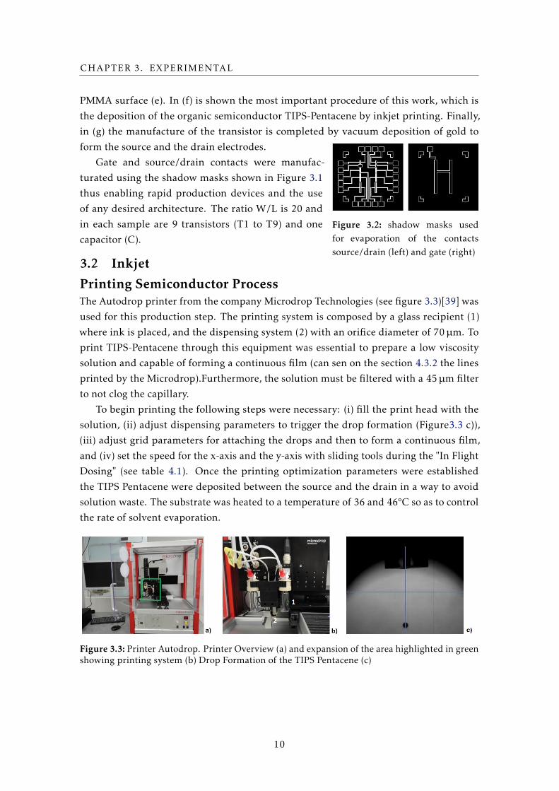
Printing Semiconductor ProcessThe Autodrop printer from the company Microdrop Technologies (see figure 3.3)[39] was
used for this production step. The printing system is composed by a glass recipient (1)
where ink is placed, and the dispensing system (2) with an orifice diameter of 70 µm. To
print TIPS-Pentacene through this equipment was essential to prepare a low viscosity
solution and capable of forming a continuous film (can sen on the section 4.3.2 the lines
printed by the Microdrop).Furthermore, the solution must be filtered with a 45 µm filter
to not clog the capillary.
To begin printing the following steps were necessary: (i) fill the print head with the
solution, (ii) adjust dispensing parameters to trigger the drop formation (Figure3.3 c)),
(iii) adjust grid parameters for attaching the drops and then to form a continuous film,
and (iv) set the speed for the x-axis and the y-axis with sliding tools during the "In Flight
Dosing" (see table 4.1). Once the printing optimization parameters were established
the TIPS Pentacene were deposited between the source and the drain in a way to avoid
solution waste. The substrate was heated to a temperature of 36 and 46°C so as to control
the rate of solvent evaporation.
Figure 3.3: Printer Autodrop. Printer Overview (a) and expansion of the area highlighted in greenshowing printing system (b) Drop Formation of the TIPS Pentacene (c)
10

Chapter 4
Analyse of the Dielectric and Active Layer
4.1 Device’s ArchitectureAs previously mentioned, the purpose of this study is to optimize the semiconductor
active layer printing with the objective to improve the technology of printed OFETs.
Previous studies of various aspects are then crucial steps to achieve this goal with success.
The first definition we need to establish is the type of architecture of our transistor. It is
well reported in the literature that Bottom Gate/Top Contact (BG/TC) structure exhibits
relatively high field effect mobility for certain p-type small molecules, as TIPS-Pentacene
[40–42].The reason for the good electric performance is often explained by the reduced
value of the contact resistance on the interface electrodes/OSC, which would be caused
by an increase in the area for charge injection [43]. In addition, it has been observed that
in case of bottom contact, the semiconductor film patterned around source and drain
leads to contacts that present a poor morphology. [44].
4.2 Dielectric LayerThe choice of dielectric is also another important step, whose dielectric properties and
processing strongly influence to the final characteristics of the printed device. The func-
tion of this layer is not only to electrically isolate the gate electrode from the source and
drain electrodes, but mainly from the semiconductor channel. An ideal dielectric layer
forms a capacitor where one electrode is the gate, and its function is to establish an elec-
tric field in the dielectric / semiconductor interface . The role of this electric field is to
control the current along the channel, both in the linear and in the saturation regimes.
In this sense, not only the bulk properties of the dielectric film are essential for the good
performance of the BG/TC, but also the roughness and the superficial energy of the di-
electric surface are extremely relevant to avoid any negative effect on the charge carrier
transport along the semiconductor layer. It has already been shown that the dielectric
interface plays a non negligible role in the molecular organization of the OSC film, which
is formed onto the dielectric layer, mainly in the molecular packing and in the crystal-
lization process [44]. Today there is a great effort of research in order to find an organic
dielectric material that has high electrical resistivity, high-value dielectric constant and
that is chemically orthogonal with the best solvents used for conjugated molecules. De-
spite the advantageous properties of Poly(vinylpyrrolidinone) (PVP), the adherence of
the semiconductor layer on PVP was very poor, which results in a non uniform and non-
crystalline deposited film. After testing other dielectrics, we decided to use the classic
PMMA. This is because, after studying different surface treatment processes and tests of
wettability, PMMA showed up as the most suitable, although their dielectric constant is
still low for a good performance as dielectric layer of an OFET. However, we believe that
it is worth insisting on PVP processing study as an alternative to PMMA. Perfilometry
11

CHAPTER 4. ANALYSE OF THE DIELECTRIC AND ACTIVE LAYER
measurements carried out with several PMMA layers showed that it exhibits an average
thickness of 540 nm.
4.2.1 Dielectric/semiconductor Interface TreatmentAs mentioned throughout the text, the interface semiconductor/dielectric plays a crucial
role in the performance of an OFET, and this subject has been extensively investigated in
the last years due to the direct impact caused on the semiconductor morphology and/or
on the generation of trap-defect at the interface causing the decrease of the charge carrier
mobility. Two aspects are determinant in the choice of the dielectric: their structural
and dielectric properties and its chemical compatibility with adequate solvents. Once
deposited the dielectric film, i. e. overcame the difficulties of the film deposition, the next
step is to eliminate the deleterious effects of electrostatic origin, which act against the
transport properties of the active layer. Thereby, in order to improve the characteristics
of the PMMA/TIPS-Pentacene interface we carried out the following procedure: i) the
PMMA was treated with UVO radiation to increase reactive groups present on its surface;
ii) a self-assembled monolayer of HMDS was evaporated on the UVO-treated PMMA
surface. This treatment improved considerably the roughness of the PMMA surface and
the wettability of the semiconductor over the dielectric layer, having as a consequence
improvement of threshold voltage and the charge carrier mobility. It was also observed
by other authors that the work function of source and drain contacts was also positively
affected [45].
12

4.2. DIELECTRIC LAYER
(a) (b)
Figure 4.1: RMS roughness of PMMA (a) without treatment; (b) with 7s UVO treatment
Figure 4.1 shows the AFM images of PMMA without (a) and with the UV-treatment (b),
which changed the root mean square (RMS) of the roughness. The RMS value increased
from approximately 0.75 nm (wihtout treatment) to 3.2 nm (with treatment). Despite the
increase in the roughness, we observed from Figure 4.1 that the UV-treatment induced an
increase in the film’s uniformity. We also studied the effect of the HMDS monolayer on
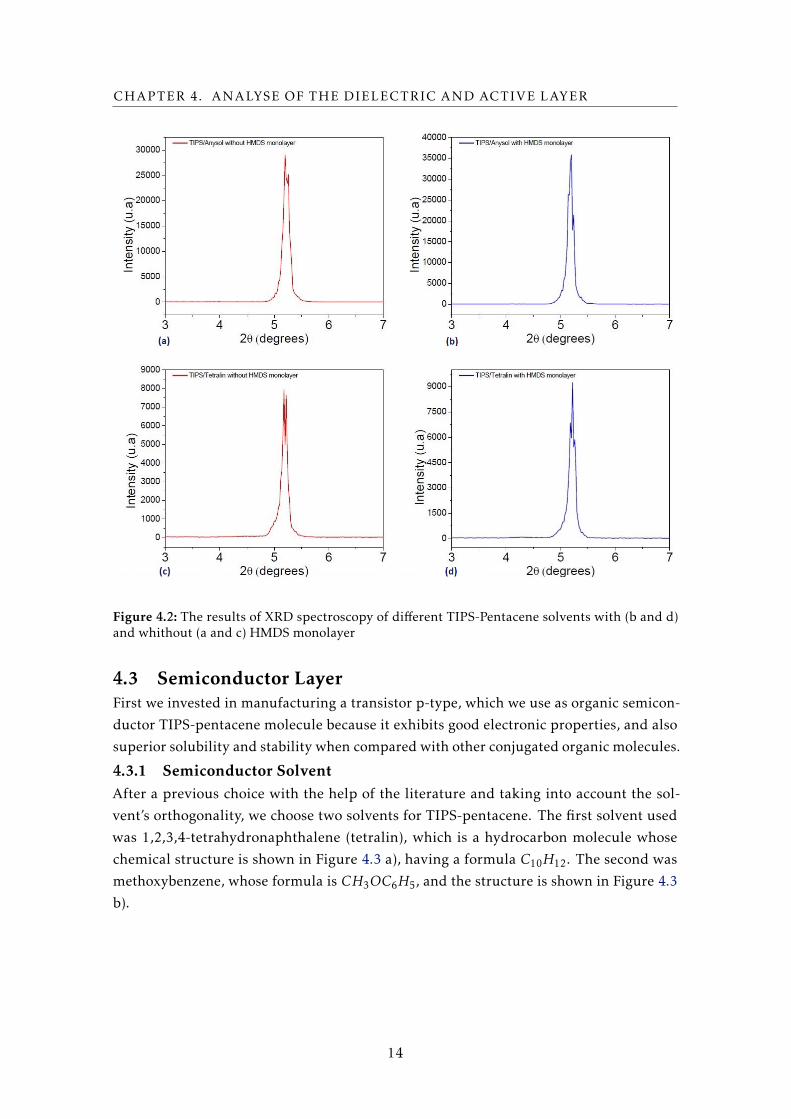
the cristallization of the TIPS pentacene film, as shown in Figure 4.2. From the analysis of
the reflection due to the (001) orientation obtained from X-Ray Diffraction spectra (XRD)
we can infer that this treatment enhanced substantially the crystallinity degree of the
deposited semiconductor films, irrespective whether the solvent for the TIPS-Pentacene
was Anaysol or Tetralin.
13
CHAPTER 4. ANALYSE OF THE DIELECTRIC AND ACTIVE LAYER
Figure 4.2: The results of XRD spectroscopy of different TIPS-Pentacene solvents with (b and d)and whithout (a and c) HMDS monolayer
4.3 Semiconductor LayerFirst we invested in manufacturing a transistor p-type, which we use as organic semicon-
ductor TIPS-pentacene molecule because it exhibits good electronic properties, and also
superior solubility and stability when compared with other conjugated organic molecules.
4.3.1 Semiconductor SolventAfter a previous choice with the help of the literature and taking into account the sol-
vent’s orthogonality, we choose two solvents for TIPS-pentacene. The first solvent used
was 1,2,3,4-tetrahydronaphthalene (tetralin), which is a hydrocarbon molecule whose
chemical structure is shown in Figure 4.3 a), having a formula C10H12. The second was
methoxybenzene, whose formula is CH3OC6H5, and the structure is shown in Figure 4.3
b).
14

4.3. SEMICONDUCTOR LAYER
Figure 4.3: Structural formula of: (a) tetralin, and (b) anisole
In theory these two solvents fulfill the basic requirements to prepare a printable
ink-TIPS Pentacene, i. e. high solubility, provided by the aromatic structure, as well as
adequate boiling point and viscosity [40, 42, 46, 47]. Aromatic solvents are suitable for
this application because their molecules solvate the π-electron of conjugated molecule,
improving the π-stacking, and hence the electrical conductivity of the formed film.
4.3.2 Printed Parameters for Semiconductor LayerSince the Microdrop printer can control a multitude of printing parameters, we per-
formed a detailed study to determine the best parameters for each TIPS Pentacene-
solution, i. e. different solutions varying the solvent (tetralin or anisole) and the con-
centration. The obtained results are shown in table 4.1.Table 4.1: Parameters used to optimize the printing TIPS-Pentacene/Tetralin and TIPS-Pentacene/Anisole
Parameters Tetralin Solvent Anisole Solvent
Drop Formation
Voltage 75-80 V 70-75 VPulse Width 30-35 µs 30-35 µsFrequency 500Hz 500HzPressure -15mbar -15mbar
Grid ParametersGrid Pattern Pattern 2 Pattern 2Grid Distance 330 µm 250 µm
"In Flight Dosing" Speed for the axes 2 mm/s 1 mm/s
It should be noted that the Grid Distance parameter, for example, for obtaining the
best results in printing multiple lines, exhibited different values of spacing drops for
tetralin and anisole. Figure 4.4 shows images for printed TIPS-Pentacene/Anisole lines
obtained using an optical microscope Olympus BX 41. From the images one can observe
that the line is formed when the spacing drop is below 350 µm, and that separated drops
are printed for spacing of drops of 400 µm and above. More specifically, for spacing drops
below and equal to 290 µm we can ensure a good line formation, i. e. lines having a good
parallelism between the lateral edges. Above 290 µm the printed lines exhibit a periodic
sinusoidal profile. Similar results were obtained for solutions of TIPS-Pentacene/Tetralin,
in which the limit between line and separated drops formation was 330 µm.
15

CHAPTER 4. ANALYSE OF THE DIELECTRIC AND ACTIVE LAYER
Figure 4.4: Printed TIPS-Pentacene/Anisole lines with different values of spacing drops
As already mentioned above, an undesirable effect difficult to be avoided during the
drop printing is the formation of the Coffee Ring effect, as shown in Figure 4.5. This effect
is caused during the solvent evaporation, which is more intense at the drop’s edges. This
evaporation asymmetry stimulates the flows of mass from the drop center to the edge,
resulting in a higher accumulation of molecules in the edges in comparison to the center
of the drop. According to Tekin et al. [48] a way to alleviate this problem, and to get more
homogeneous films is to use a mixture of solvents having high and low boiling points. In
such mixture, the solvent with a lower boiling point would evaporate more slowly, and
then gradually decreasing the flows of mass. A suggestion for the continuity of this work
is to find a good solvent for the TIPS-Pentacene that has a
Figure 4.5: Coffee Ring Effect
lower boiling point in comparison to tetralin
(207°C) or anisole (154°C).
Once the parameters that optimize the TIPS-
pentacene printing were defined, and from the anal-
ysis of the best printed lines, both in using Tetralin
or Anisole as solvent (Figure 4.4), we reached some
important remarks. First, the TIPS-Pentacene printed
line (in anisole) presented na undesirable result aris-
ing from the Coffe Ring effect (Figure 4.6(a)). Second,
crystalline structures were formed in printed lines (in
tetralin), which is crucial for a good performance of
the charge transport along the semiconductor channel, as already described in Section
1.5. This crystallinity is clearly shown in Figure 4.6(b), which also indicates that the
long crystallites were arranged in an organized manner forming a herringbone structure.
The conclusion obtained from these two points is that the printed line of TIPS-pentacene
dissolved in tetralin, despite its highest boiling point, is more efficient to built a semi-
conductor channel for an OFET. This can be explained by the fact that the substrate was
heated during the printing procedure.
16
4.4. STRUCTURE AND MORPHOLOGY OF THE PRINTED LAYERS
(a) (b)
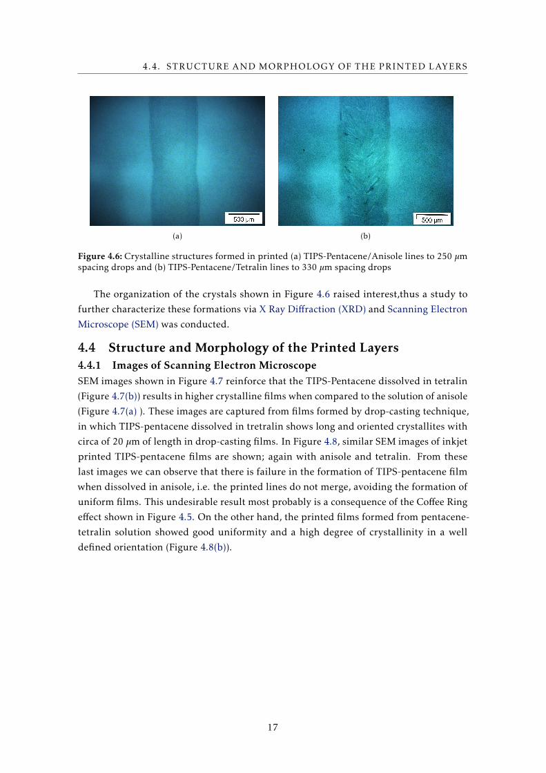
Figure 4.6: Crystalline structures formed in printed (a) TIPS-Pentacene/Anisole lines to 250 µmspacing drops and (b) TIPS-Pentacene/Tetralin lines to 330 µm spacing drops
The organization of the crystals shown in Figure 4.6 raised interest,thus a study to
further characterize these formations via X Ray Diffraction (XRD) and Scanning Electron
Microscope (SEM) was conducted.
4.4 Structure and Morphology of the Printed Layers4.4.1 Images of Scanning Electron MicroscopeSEM images shown in Figure 4.7 reinforce that the TIPS-Pentacene dissolved in tetralin
(Figure 4.7(b)) results in higher crystalline films when compared to the solution of anisole
(Figure 4.7(a) ). These images are captured from films formed by drop-casting technique,
in which TIPS-pentacene dissolved in tretralin shows long and oriented crystallites with
circa of 20 µm of length in drop-casting films. In Figure 4.8, similar SEM images of inkjet
printed TIPS-pentacene films are shown; again with anisole and tetralin. From these
last images we can observe that there is failure in the formation of TIPS-pentacene film
when dissolved in anisole, i.e. the printed lines do not merge, avoiding the formation of
uniform films. This undesirable result most probably is a consequence of the Coffee Ring
effect shown in Figure 4.5. On the other hand, the printed films formed from pentacene-
tetralin solution showed good uniformity and a high degree of crystallinity in a well
defined orientation (Figure 4.8(b)).
17

CHAPTER 4. ANALYSE OF THE DIELECTRIC AND ACTIVE LAYER
(a) of TIPS-Pentacene/Anisole (b) of TIPS-Pentacene/Tetralin
Figure 4.7: Analyzed SEM image and crystalization of an thin films formed by drop castingtechnique
(a) of TIPS-Pentacene/Anisole
A(b) of TIPS-Pentacene/Tetralin
Figure 4.8: Analyzed SEM image and crystalization of an thin films formed by inkjet printing
4.4.2 Wide-Angle X-ray DiffractionWide-Angle X-ray Diffraction (WAXD) patterns of TIPS-pentacene films were obtained by
a Rigaku Rotaflex RU 200B instrument (Cu Kα radiation, λ = 1.5418Å), operating with
40 kV and 80 mA. The films were deposited onto a PMMA previously functionalized
with HMDS, supported by a glass substrate. Figures 4.9(a) and 4.9(b) show, respectively,
the X-ray diffraction pattern of the nude substrate (glass) and that of the substrate coated
with a thin film of functionalized PMMA. The amorphous characteristic is evidenced by
the broad peak centered 2θ equal to 24°. When a printed thin film of TIPS-Pentacene is
deposited on the top of the HMDS-PMMA (that whose WAXD is shown in Figure 4.9(b)),
the new recorded X-ray diffractogram is completely different, as shown in Figure 4.10(a).
This diffractogram confirms the high crystallinity degree of the printed TIPS-pentacene
from a tetralin solution. Just for comparison, we present a diffraction pattern obtained
from a thick film of TIPS-Pentacene (Figure 4.10(b)), also from a tetralin solution, which
shows the same diffraction peaks displayed in Figure 4.10(a).
18

4.4. STRUCTURE AND MORPHOLOGY OF THE PRINTED LAYERS
(a) (b)
Figure 4.9: WAXD obtained from: a) nude glass substrate; and b) the same substrate coated withPMMA functionalized with HMDS.
Anthony et al. [49] Single-crystal TIPS-Pentacene has a triclinic structure with unit
cell parameters a = 7.5650Å, b = 7.7500Å, c = 16.835Å, α = 89.15°, β = 92.713°, and
γ = 83.63°. The peak observed at about 5.2° corresponds to intermolecular spacing of
16.8Å, indicating preferential orientation of (001)-axis normal to the surface. The peaks
that appeared at 10.4° and 15.8° were identified with the (002) and (003) orientation,
respectively.
(a) (b)
Figure 4.10: WADX obtained from TIPS-pentacene film deposited by: a)inkjet printing on thesubstrate coated with PMMA functionalized with HMDS; b)drop casting
19


Chapter 5
OFETs and Inverter
Since the purpose of this work is to take the first steps for printing logic circuits made
with organic semiconductors, the first and important step is to master the printing of
the active layer of an organic transistor. This chapter shows the results obtained with a
p-type OFET and the application in a p-MOS inverter. In the last section we present the
first results with a n-OFET. The continuity of research in these two transistors, n and p
types, will open numerous possibilities in the area of printed organic circuits, especially
from the printing of an organic complementary circuit.
5.0.1 OFETs: Drain current (ID) versus source-drain voltage (VD)The quality of inkjet printed TIPS-Pentacene films as active layer in the p-OFET channel
is directly affected by the solvent used in the electronic ink, as shown in Figure 5.1. Figure
5.1(a) shows that the drain current (ID ) versus source-drain voltage (VD ), having different
gate voltages, when anisole was used as solvent presented a significant leakage current.
On the other hand, ID x VD responses obtained with similar transistor now using TIPS-
Pentacene dissolved in tetralin, not only eliminated the undesirable leakage current, but
also exhibited higher drain current (almost one order of magnitude higher), as shown
in Figure 5.1(b). This improvement is a direct consequence of the better printed film
as discussed in the previous section when tetralin is used as the solvent. This solution
produced more uniform and crystalline films. It is important to remark that the relatively
high values for the operation voltage are due to the low dielectric constant of the PMMA.
In this research area the search for better organic materials to be used as a dielectric layer
for OFETs is the challenge to be overcome currently.
(a) (b)
Figure 5.1: Drain current vs Drain-source voltage of p-OFETs: a) TIPS-pentacene dissolved inAnisole; b) TIPS-pentacene dissolved in Tetraline
21
CHAPTER 5. OFETS AND INVERTER
5.1 p-OFETs-tetralinSince tetralin showed to be a superior solvent for TIPS-pentacene, we seek to optimize
the performance of the printed transistors by varying the rate of solvent evaporation. To
do this, the substrate was heated during the deposition of TIPS-pentacene into transistor
channel. This was possible due to heating feature available in the Microdrop printer.
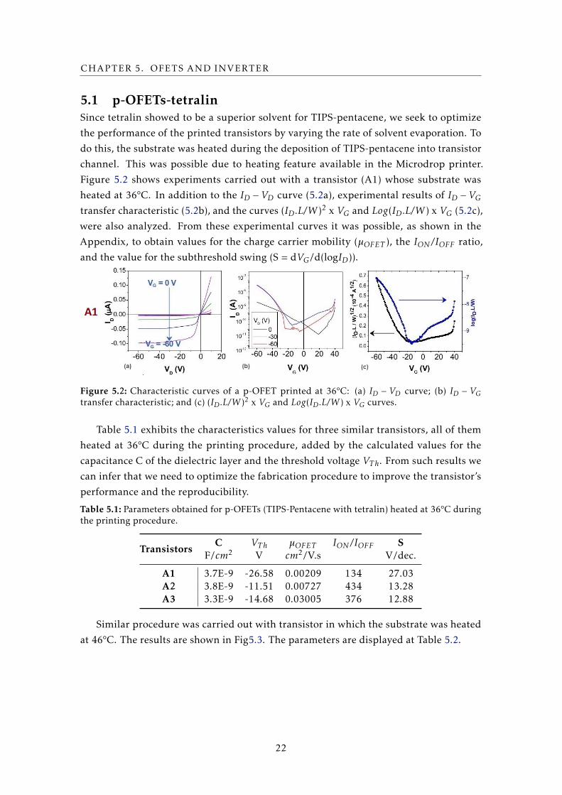
Figure 5.2 shows experiments carried out with a transistor (A1) whose substrate was
heated at 36°C. In addition to the ID −VD curve (5.2a), experimental results of ID −VGtransfer characteristic (5.2b), and the curves (ID .L/W )2 x VG and Log(ID .L/W ) x VG (5.2c),
were also analyzed. From these experimental curves it was possible, as shown in the
Appendix, to obtain values for the charge carrier mobility (µOFET ), the ION /IOFF ratio,
and the value for the subthreshold swing (S = dVG/d(logID )).
Figure 5.2: Characteristic curves of a p-OFET printed at 36°C: (a) ID − VD curve; (b) ID − VGtransfer characteristic; and (c) (ID .L/W )2 x VG and Log(ID .L/W ) x VG curves.
Table 5.1 exhibits the characteristics values for three similar transistors, all of them
heated at 36°C during the printing procedure, added by the calculated values for the
capacitance C of the dielectric layer and the threshold voltage VT h. From such results we
can infer that we need to optimize the fabrication procedure to improve the transistor’s
performance and the reproducibility.
Table 5.1: Parameters obtained for p-OFETs (TIPS-Pentacene with tetralin) heated at 36°C duringthe printing procedure.
TransistorsC VT h µOFET ION /IOFF S
F/cm2 V cm2/V.s V/dec.
A1 3.7E-9 -26.58 0.00209 134 27.03A2 3.8E-9 -11.51 0.00727 434 13.28A3 3.3E-9 -14.68 0.03005 376 12.88
Similar procedure was carried out with transistor in which the substrate was heated
at 46°C. The results are shown in Fig5.3. The parameters are displayed at Table 5.2.
22

5.2. INVERTER CHARACTERIZATION
Figure 5.3: Characteristic curves of a p-OFET printed at 46°C: (a) ID − VD curve; (b) ID − VGtransfer characteristic; and (c) (ID .L/W )2 x VG and Log(ID .L/W ) x VG curves.
Table 5.2: Parameters obtained for p-OFETs (TIPS-Pentacene with tetralin) heated at 46°C duringthe printing procedure.
TransistorsC VT h µOFET ION /IOFF S
F/cm2 V cm2/V.s V/dec.
B1 9.77E-10 -14.89 0.17066 10110 4.98B2 9.77E-10 -20.44 0.30274 7672 6.81B3 1.55E-8 -22.43 0.01823 52950 1.68
We observed that the capacitance did not change significantly from one transistor to
another, at least for those heated at 36°C. For those heated at 46°C, only the transistor B3
showed a different value for the capacitance. On the other hand, the threshold voltage was
more uniform for the transistors heated at 46°C, and also they presented higher values
for the mobility, ION /IOFF ratio and subthreshold swing S.
5.2 Inverter CharacterizationThe main function of an inverter circuit is to invert the applied input signal. A simple
inverter can be constructed by using a single p-OFET coupled with a resistor, as depicted
in Figure 5.4, in which the load resistance is in series with the drain electrode and the
source is grounded. The opposite side of the resistor is connected to the to the supply
voltage (VDD ), and when Vin = 0 (logic 0), the transistor is off and no current flows through
the resistor, and Vout ≡ 1. However, for Vin = VDD (logic 1) , it results in Vout ≡ 0 (Table
5.3).
Figure 5.4: PMOS inverter with a resistor load
23

CHAPTER 5. OFETS AND INVERTER
Table 5.3: Truth Table
Vin Vout
0 11 0
For our experiment we used a resistor-transistor inverter circuit first with a VDD = 60
V, and varied the RL from 50 to 300 MΩ, sweeping the Vin from -60 V to zero. The result
is shown in Figure 5.5a. Figure 5.5b show similar Vout X Vin curve for a RL = 300 MΩ, for
different values of VDD (from 20 to 60 V); amd Figure 5.5c shows the gain curve of this
circuit for VDD = 60 V and RL = 300 MΩ.
Figure 5.5: Curves of voltage transfer characteristics of the digital inverter. (a) Effect of resistancefor VDD = 60V ; (b) Effect of variation of tension for R=300MΩ; (c) VTC curve with drive voltagegain for VDD = 60V and R=300MΩ
5.3 n-OFETHere we present preliminary results on n-OFET manufacturing by inkjet printing. The
structure chosen for the n-OFET was also BG / TC, and the semiconductor was the conju-
gated molecule P(NDI2OD-T2) (ActiveInk™N2200), shown in Figure 5.6 This molecule
was dissolved in p-xylene in a concentration of 3 mg/ml, and after printing it in the
channel, the transistor was annealed at 200°C during 30 minutes.
Figure 5.7 displays results of the same experiments as carried out with p-OFETs, i. e.
the ID-VD curve (5.7a), the ID-VG transfer characteristic (5.7b), and the curves (ID .L/W )2
24

5.3. N-OFET
x VG and Log(ID .L/W ) x VG (5.7c).
Figure 5.6: Molecular structure of P(NDI2OD-T2)
Figure 5.7: Characteristic curves of a n-OFET: (a) ID −VD curve; (b) ID −VG transfer characteristic;and (c) (ID .L/W )2 x VG and Log(ID .L/W ) x VG curves.)
Table 5.4: Parameters obtained for n-OFETs
TransistorsC VT h µOFET ION /IOFF S
F/cm2 V cm2/V.s V/dec.
C1 8.59E-9 10.13 1.35E-4 21 10.99C2 8.59E-9 9.67 0.00138 474 3.28C3 8.59E-9 -21.50 3.26E-4 0.17 56.31
Despite the Field-effect operation shown by the family of curves displayed in Figure
5.7a, the parameters extracted from three first fabricated transistors are still very poor
and need improvements. However, being these results the first, they are promising. With
the improvement of the performance of n and p OFETs, it will be possible in a near future
to build printed complementary organic circuits.
25


Chapter 6
Conclusions and Final Remarks
Printed electronics is a new branch inside processing and novel materials for electronics.
This area is growing fast and is revealing a promising and huge market in the near future.
Several printing techniques for electronics have been developed in the last years, as offset
lithography, flexography, rotogravure, serigraphy, and Inkjet. In this scenario, this thesis
proposes to use inkjet printing technique to deposit organic films as the semiconductor
layer in the channel of OFETs. First we use the TIPS-Pentacene, which is an p-type
organic semiconductor, to conduct a study of the best solvent for having the adequate
fluidic parameters to achieve good printed thin films in the channel. We identified the
tetralin as an organic solvent that fits well the required printing conditions. We used an
Autrodrop model of Microdrop company as the printer, which uses a Drop-on-Demand
system via a piezoelectric ejector. The organic film was printed over a thin film of PMMA,
which played the role of the dielectric layer in the transistor. In order to optimize the
printing process of TIPS-Pentacene thin-films applied on OFET Technology, an extensive
study boarding several parameters was performed:
(i) BG/TC architecture was chosen due to the high field effect mobility present by the
devices. This architecture presents a low contact area for charge injection, which leads to
a reduced contact resistance. The combination of these two parameters originated devices
with a good electrical performance;
(ii) The choice of polymeric material used as insulator between the gate electrode and
the semiconductor channel was limited to a few materials. PMMA was choised due to it
excellent properties as electrical insulator. However, PMMA has a low dielectric constant.
Today, new polymers with higher values of dielectric constant are emerging in the market,
which should improve the performance of organic transistors, especially in lowering its
operating voltage;
(iii) Since the morphology of the dielectric/semiconductor interface is a crucial param-
eter for the device’s performance, a surface treatment consisting of UV-Ozone radiation
followed by a deposition of a HMDS monolayer was applied to this interface. AFM results
show that the roughness’s RMS suffered an increase after the applied treatment (0.75 to
3.2 nm), consequence of the added functional groups that result from the UVO treatment.
As for the XRD spectra (with and without HMDS), we can conclude that the crystallinity
of TIPS-Pentacene is increased when HMDS is added to the interface;
(iv) The TIPS-Pentacene film’s morphology has a strong dependence on the chosen
solvent. In order to achieve the most suitable morphology, a detailed study to the TIPS-
Pentacene was carried out using microscopy techniques and WAXD. Besides providing
a better structural morphology with desired electrical properties, the used solvent needs
to be an orthogonal solvent for the dielectric layer (PMMA). We found that the solvent
tetralin provided well organized TIPS-Pentacene films with a high crystallinity degree,
27

CHAPTER 6. CONCLUSIONS AND FINAL REMARKS
making this the most suitable solvent;
(v) The transistors were fabricated with two different substrate temperatures (36 and
46°C) and further characterize be means of Drain current vs Drain-source voltage, IDVG transfer characteristic,(ID .L/W )2 x VG and Log(ID .L/W ) x VG curves. The transistors
presented higher values of mobility and ION /IOFF ratio at 46°C than at 36°C. The obtained
mobility and values ION /IOFF ratio are in concordance with the ones described in the
literature. Interestingly, the subthreshold voltage (S) suffered a significant increase (-
10−3 to 1 V/dec), which is not good for the performance of the transistors, since higher
values of S result in higher gate voltages required to improve the drain current in one
decade.
Using the most suitable parameters determined in the previous studies, we were able
to fabricate a p-OFET in an resistor-transistor inverter with a gain of 5.3.
The literature is abundant in organic semiconductor of p-type, but only recently good
and processable n-type organic molecules have been synthesized. What we intend for the
continuity of this work is to build p-OFETs and n-OFETS with similar characteristics, so to
pave the way for the fabrication of a complementary organic circuits, a CMOS type. With
this in mind, we obtained the first results of a printed n-OFETs using the P(NDI2OD-T2)
molecule as semiconductor. We succedded in keeping the same geometric architecture
used for the p-OFET (BG/TC), since we can use the same mask and the same substrate
for printing both the p and n OFET side by side.
These preliminary results showed that we are in the right direction, and for future
developments the aim is to dominate the fabrication of a printed n-OFET that matches
the characteristics of a p-OFET, so that the fabrication of a complementary organic circuit
can be achieved.
28

Bibliography
[1] J. R. Sheats, D. Biesty, J. Noel, and G. N. Taylor. “Printing technology for ubiquitous
electronics”. In: Circuit World 36.2 (2010), pp. 40–47. issn: 0305-6120. doi:
10.1108/03056121011041690.
[2] A. Loi, L. Basiric??, P. Cosseddu, S. Lai, M. Barbaro, A. Bonfiglio, P. Maiolino, E.
Baglini, S. Denei, F. Mastrogiovanni, and G. Cannata. “Organic bendable and
stretchable field effect devices for sensing applications”. In: IEEE Sensors Jour-nal 13.12 (2013), pp. 4764–4772. issn: 1530437X. doi: 10.1109/JSEN.2013.
2273173.
[3] J. Fernandez-Salmeron, A. Rivadeneyra, M. A. C. Rodriguez, L. F. Capitan-Vallvey,
and A. J. Palma. “HF RFID Tag as Humidity Sensor: Two Different Approaches”.
In: IEEE Sensors Journal 15.10 (2015), pp. 5726–5733. issn: 1530-437X. doi: 10.
1109/JSEN.2015.2447031.
[4] R. S. Deol, H. W. Choi, M. Singh, and G. E. Jabbour. “Printable displays and light
sources for sensor applications: A review”. In: IEEE Sensors Journal 15.6 (2015),
pp. 3186–3195. issn: 1530437X. doi: 10.1109/JSEN.2014.2378144.
[5] K. J. Baeg, D. Khim, J. H. Kim, M. Kang, I. K. You, D. Y. Kim, and Y. Y. Noh.
“Improved performance uniformity of inkjet printed n-channel organic field-effect
transistors and complementary inverters”. In: Organic Electronics: physics, materials,applications 12.4 (2011), pp. 634–640. issn: 15661199. doi: 10.1016/j.orgel.
2011.01.016.
[6] S. Lim, B. Kang, D. Kwak, W. H. Lee, J. A. Lim, and K. Cho. “Inkjet-printed reduced
graphene oxide/poly(vinyl alcohol) composite electrodes for flexible transparent
organic field-effect transistors”. In: Journal of Physical Chemistry C 116.13 (2012),
pp. 7520–7525. issn: 19327447. doi: 10.1021/jp203441e.
[7] A. Tsumura, H. Koezuka, and T. Ando. “Macromolecular electronic device: Field-
effect transistor with a polythiophene thin film”. In: Applied Physics Letters 49.18
(1986), pp. 1210–1212. issn: 00036951. doi: 10.1063/1.97417.
[8] G. Horowitz, X. Peng, D. Fichou, and F. Garnier. “The oligothiophene-based field-
effect transistor: How it works and how to improve it”. In: Journal of Applied Physics67.1 (1990), pp. 528–532. issn: 00218979. doi: 10.1063/1.345238.
[9] M. Kitzler, X. Xie, S. Roither, A. Scrinzi, and A. Baltuska. “Angular encoding
in attosecond recollision”. In: New Journal of Physics 10 (2008), pp. 0–13. issn:
13672630. doi: 10.1088/1367-2630/10/2/025029.
[10] G Horowitz. “Organic field-effect transistors”. In: Advanced Materials 10.5 (1998),
pp. 365–377. issn: 0935-9648. doi: 10.1002/(sici)1521-4095(199803)10:
5<365::aid-adma365>3.0.co;2-u.
[11] C. F. O. Graeff, R. M. Faria, F. E. G. Guimarães, and R. K. Onmori. “Field effect
transistor using poly (o-metoxyaniline) films”. In: (1999), pp. 151–153.
29
BIBLIOGRAPHY
[12] S. Allard, M. Forster, B. Souharce, H. Thiem, and U. Scherf. “Organic semicon-
ductors for solution-processable field-effect transistors (OFETs)”. In: AngewandteChemie - International Edition 47.22 (2008), pp. 4070–4098. issn: 14337851. doi:
10.1002/anie.200701920.
[13] B. Kumar, B. K. Kaushik, and Y. S. Negi. “Organic Thin Film Transistors: Structures,
Models, Materials, Fabrication, and Applications: A Review”. In: Polymer Reviews54.1 (2014), pp. 33–111. issn: 1558-3724. doi: 10.1080/15583724.2013.848455.
[14] C. H. Kim, Y. Bonnassieux, and G. Horowitz. “Compact DC modeling of organic
field-effect transistors: Review and perspectives”. In: IEEE Transactions on ElectronDevices 61.2 (2014), pp. 278–287. issn: 00189383. doi: 10.1109/TED.2013.
2281054.
[15] C. Liu, Y. Xu, and Y. Y. Noh. “Contact engineering in organic field-effect transistors”.
In: Materials Today 18.2 (2015), pp. 79–96. issn: 13697021. doi: 10.1016/j.
mattod.2014.08.037.
[16] A. Hepp, H. Heil, W. Weise, M. Ahles, R. Schmechel, and H. von Seggern. “Light-
Emitting Field-Effect Transistor Based on a Tetracene Thin Film”. In: Physical Re-view Letters 91.15 (2003), p. 157406. issn: 0031-9007. doi: 10.1103/PhysRevLett.
91.157406.
[17] E. C. P. Smits, S. Setayesh, T. D. Anthopoulos, M. Buechel, W. Nijssen, R. Coehoorn,
P. W. M. Blom, B. De Boer, and D. M. De Leeuw. “Near-infrared light-emitting
ambipolar organic field-effect transistors”. In: Advanced Materials 19.5 (2007),
pp. 734–738. issn: 09359648. doi: 10.1002/adma.200600999.
[18] T. Sekitani, U. Zschieschang, H. Klauk, and T. Someya. “Flexible organic transis-
tors and circuits with extreme bending stability.” In: Nature materials 9.12 (2010),
pp. 1015–1022. issn: 1476-1122. doi: 10.1038/nmat2896.
[19] G. Gelinck, P. Heremans, K. Nomoto, and T. D. Anthopoulos. “Organic transistors
in optical displays and microelectronic applications”. In: Advanced Materials 22.34
(2010), pp. 3778–3798. issn: 09359648. doi: 10.1002/adma.200903559.
[20] L. M. Dumitru, K. Manoli, M. Magliulo, G. Palazzo, and L. Torsi. “Low-voltage
solid electrolyte-gated OFETs for gas sensing applications”. In: MicroelectronicsJournal 45.12 (2014), pp. 1679–1683. issn: 00262692. doi: 10.1016/j.mejo.
2014.05.017.
[21] G. C. Faria, D. T. Duong, A Salleo, C. A. Polyzoidis, S Logothetidis, J Rivnay, R
Owens, and G. G. Malliaras. “Organic electrochemical transistors as impedance
biosensors”. In: Mrs Communications 4.4 (2014), pp. 189–194. issn: 2159-6859.
doi: 10.1557/mrc.2014.35.
30
BIBLIOGRAPHY
[22] V. Coropceanu, J. Cornil, D. A. da Silva Filho, Y. Olivier, R. Silbey, and J.-L. Brédas.
“Charge transport in organic semiconductors”. In: Chem. Rev. 107 (2007), pp. 926–
952. issn: 03401022. doi: 10.1007/128_2011_218.
[23] O. V. Mikhnenko, P. W. M. Blom, and T.-Q. Nguyen. “Exciton diffusion in organic
semiconductors”. In: Energy Environ. Sci. 8 (2015), pp. 1867–1888. issn: 1754-
5692. doi: 10.1039/c5ee00925a.
[24] C. Huang. “Organic Semiconductor for Flexible Electronics”. PhD thesis.
[25] D. Alfredo and D. S. Pereira. “Control of a White Organic Light Emitting Diode ’ s
emission parameters using a single doped RGB active layer”. In: September (2015).
issn: 09215107. doi: 10.1016/j.mseb.2016.07.004.
[26] D. Cibis. “Influencing Parameters in Droplet Formation for DoD Printing of Con-
ductive Inks”. In: Proc. of the 4th Int. Conf. of Ceramic (2008), pp. 417–423.
[27] M. Singh, H. M. Haverinen, P. Dhagat, and G. E. Jabbour. “Inkjet printing-process
and its applications”. In: Advanced Materials 22.6 (2010), pp. 673–685. issn:
09359648. doi: 10.1002/adma.200901141.
[28] “Inkjet-printed line morphologies and temperature control of the coffee ring ef-
fect”. In: Langmuir 24.5 (2008), pp. 2224–2231. issn: 07437463. doi: 10.1021/
la7026847.
[29] J. A. Lim, W. H. Lee, H. S. Lee, J. H. Lee, Y. D. Park, and K. Cho. “Self-organization
of ink-jet-printed triisopropylsilylethynyl pentacene via evaporation-induced flows
in a drying droplet”. In: Advanced Functional Materials 18.2 (2008), pp. 229–234.
issn: 1616301X. doi: 10.1002/adfm.200700859.
[30] H. Li, G. Giri, J. B.-H. Tok, and Z. Bao. “Toward high-mobility organic field-
effect transistors: Control of molecular packing and large-area fabrication of single-
crystal-based devices”. In: MRS Bulletin 38.01 (2013), pp. 34–42. issn: 1938-1425.
doi: doi:10.1557/mrs.2012.309.
[31] J. E. Anthony. Research Interests of the Anthony Group. url: http://www.chem.uky.
edu/research/Anthony/welcome.html (visited on 09/11/2016).
[32] Y. Y. Lin, D. J. Gundlach, S. F. Nelson, and T. N. Jackson. “Stacked pentacene layer
organic thin-film transistors with improved characteristics”. In: IEEE ElectronDevice Letters 18.12 (1997), pp. 606–608. issn: 07413106. doi: 10.1109/55.
644085.
[33] Z. Cui. Printed Electronics: Materials, Technologies and Applications - Zheng Cui -Google Livros. WILEY Higher Education Press, 2016.
[34] Z. Bao, J. Locklin, and G. Horowitz. Organic field-effect transistors. Vol. 10. 5. 2007,
pp. 365–377. isbn: 10: 0-8493-8080-4. doi: 10.1002/(SICI)1521-4095(199803)
10:5<365::AID-ADMA365>3.0.CO;2-U.
31

BIBLIOGRAPHY
[35] Z. Stewart. “Organic Thin-Film Transistors and TIPS- Pentacene”. In: UKnowledge(2013).
[36] J. E. Anthony. “The larger acenes: Versatile organic semiconductors”. In: Ange-wandte Chemie - International Edition 47.3 (2008), pp. 452–483. issn: 14337851.
doi: 10.1002/anie.200604045.
[37] S. K. Park, D. A. Mourey, J. I. Han, J. E. Anthony, and T. N. Jackson. “Environmental
and operational stability of solution-processed 6,13-bis(triisopropyl-silylethynyl)
pentacene thin film transistors”. In: Organic Electronics: physics, materials, applica-tions 10.3 (2009), pp. 486–490. issn: 15661199. doi: 10.1016/j.orgel.2009.02.
007.
[38] Y. Yan, L. B. Huang, Y. Zhou, S. T. Han, L. Zhou, Q. Sun, J. Zhuang, H. Peng, H. Yan,
and V. A. L. Roy. “Surface Decoration on Polymeric Gate Dielectrics for Flexible
Organic Field-Effect Transistors via Hydroxylation and Subsequent Monolayer Self-
Assembly”. In: ACS Applied Materials and Interfaces 7.42 (2015), pp. 23464–23471.
issn: 19448252. doi: 10.1021/acsami.5b05363.
[39] Microdrop Technologies. “Autodrop compact micro dispensing system”. 2014.
[40] X. Wang, M. Yuan, X. Xiong, M. Chen, M. Qin, L. Qiu, H. Lu, G. Zhang, G. Lv, and
A. H. W. Choi. “Process optimization for inkjet printing of triisopropylsilylethynyl
pentacene with single-solvent solutions”. In: Thin Solid Films 578 (2015). issn:
00406090. doi: 10.1016/j.tsf.2015.02.004.
[41] H. Klauk, M. Halik, U. Zschieschang, G. Schmid, W. Radlik, and W. Weber. “High-
mobility polymer gate dielectric pentacene thin film transistors”. In: Journal ofApplied Physics 92.9 (2002), pp. 5259–5263. issn: 00218979. doi: 10.1063/1.
1511826.
[42] M. W. Lee, G. S. Ryu, Y. U. Lee, C. Pearson, M. C. Petty, and C. K. Song. “Control of
droplet morphology for inkjet-printed TIPS-pentacene transistors”. In: Microelec-tronic Engineering 95 (2012), pp. 1–4. issn: 01679317. doi: 10.1016/j.mee.2012.
01.006.
[43] C. Reese, M. Roberts, M.-m. Ling, and Z. Bao. Organic Thin-Film Transistors (OTFTs).2004.
[44] N. L. Vaklev, R. Miller, B. V. O. Muir, D. T. James, R. Pretot, P. Van Der Schaaf, J.
Genoe, J. S. Kim, J. H. G. Steinke, and A. J. Campbell. “High-Performance Flexible
Bottom-Gate Organic Field-Effect Transistors with Gravure Printed Thin Organic
Dielectric”. In: Advanced Materials Interfaces 1 (2014). issn: 21967350. doi: 10.
1002/admi.201300123.
[45] F. Gholamrezaie. “Self-assembled Monolayers in Organic Electronics”. PhD thesis.
University of Groningen, The Netherlands, 2012, p. 128. isbn: 9789036756914.
32

BIBLIOGRAPHY
[46] J. A. Lim, W. H. Lee, D. Kwak, and K. Cho. “Evaporation-Induced Self-Organization
of Inkjet-Printed Organic Semiconductors on Surface-Modified Dielectrics for High-
Performance Organic Transistors”. In: Langmuir 25.9 (2009), pp. 5404–5410. issn:
07437463. doi: 10.1021/la804269q.
[47] S.-I. Shin, J.-H. Kwon, H. Kang, and B.-K. Ju. “Solution-processed 6,13-
bis(triisopropylsilylethynyl) (TIPS) pentacene thin-film transistors with a polymer
dielectric on a flexible substrate”. In: Semiconductor Science and Technology 23
(2008), p. 085009. issn: 0268-1242. doi: 10.1088/0268-1242/23/8/085009.
[48] E. Tekin, B.-J. de Gans, and U. S. Schubert. “Ink-jet printing of polymers ? from
single dots to thin film libraries”. In: Journal of Materials Chemistry 14.17 (2004),
p. 2627. issn: 0959-9428. doi: 10.1039/b407478e.
[49] J. E. Anthony, J. S. Brooks, David L. Eaton, and S. R. Parkin. “Functionalized
Pentacene: Improved Electronic Properties from Control of Solid-State Order”. In:
222.11 (2001), pp. 9482–9483. doi: 10.1021/JA0162459.
[50] J Zaumseil and H Sirringhaus. “Electron and Ambipolar Transport in Organic
Field-Effect Transistors”. In: Chemical Reviews 107 (2007), pp. 1296–1323. issn:
0009-2665. doi: 10.1021/cr0501543.
33

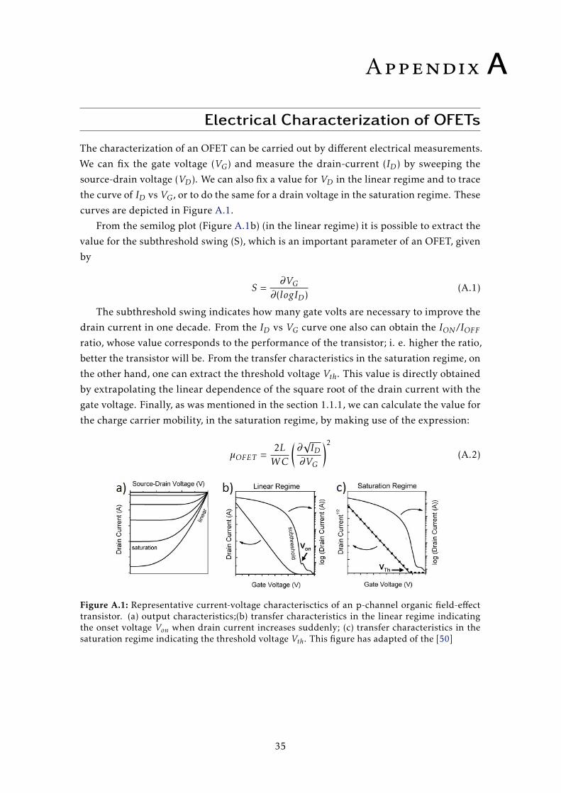
Appendix A
Electrical Characterization of OFETs
The characterization of an OFET can be carried out by different electrical measurements.
We can fix the gate voltage (VG) and measure the drain-current (ID) by sweeping the
source-drain voltage (VD ). We can also fix a value for VD in the linear regime and to trace
the curve of ID vs VG, or to do the same for a drain voltage in the saturation regime. These
curves are depicted in Figure A.1.
From the semilog plot (Figure A.1b) (in the linear regime) it is possible to extract the
value for the subthreshold swing (S), which is an important parameter of an OFET, given
by
S =∂VG
∂(logID )(A.1)
The subthreshold swing indicates how many gate volts are necessary to improve the
drain current in one decade. From the ID vs VG curve one also can obtain the ION /IOFFratio, whose value corresponds to the performance of the transistor; i. e. higher the ratio,
better the transistor will be. From the transfer characteristics in the saturation regime, on
the other hand, one can extract the threshold voltage Vth. This value is directly obtained
by extrapolating the linear dependence of the square root of the drain current with the
gate voltage. Finally, as was mentioned in the section 1.1.1, we can calculate the value for
the charge carrier mobility, in the saturation regime, by making use of the expression:
µOFET =2LWC
(∂√ID
∂VG
)2
(A.2)
Figure A.1: Representative current-voltage characterisctics of an p-channel organic field-effecttransistor. (a) output characteristics;(b) transfer characteristics in the linear regime indicatingthe onset voltage Von when drain current increases suddenly; (c) transfer characteristics in thesaturation regime indicating the threshold voltage Vth. This figure has adapted of the [50]
35


2016
Optimizationof
PrintedTIP
S-Pe
ntaceneThin-Film
Applied
onOFE
Ttech
nolog
ySo
fia
Mar
tins