optimized design platform for high speed digital filter ... · optimized design platform for high...
TRANSCRIPT

19
Optimized Design Platform for High Speed
Digital Filter using Folding Technique
1Shreyas Patel
,
2Prof.J.S. Rani Alex
1Department of SENSE, VIT University, Chennai, India
2Department of SENSE, VIT University, Chennai, India
ABSTRACT
Implementation of DSP system must satisfy the sampling rate constraint and must require less space
and power consumption. Thus finding a reasonable solution to optimize design platform using
different algorithm is much needed. In this paper an optimized platform is designed by lifetime
analysis which is one of the techniques of folding algorithm for minimizing the registers such that
synthesizable RTL is obtained. Folding techniques can be used for the synthesis of DSP architecture
that can be operated using single or multiple clocks with less number of registers and functional units
resulting in an integrated circuit with usage of small silicon area. A technique is presented for
computing the minimum number of registers, allocating the data to these registers and obtains
synthesizable RTL code for folded architecture.
Keywords: Folding Architecture, RTL (Register Transfer Logic), Register Minimization, Lifetime
Analysis.
I. INTRODUCTION
In today's VLSI world, Designers had to design circuit with high performance and with less area and
this to be done with a rapid design time. CAD tool play a very important role in achieving this
requirement. ASIC design process start with given specification, from these high level functional
block is obtained. These can be later used for obtaining circuit level device. In present work designed
of 3-tap IIR filter model is design in MATLAB SIMULINK using XILINX block set, System
generator which generate automatic synthesizable RTL code and design specification report of speed,
area, power and registers. Folding technique provide a mean for trading area for time in a DSP
architecture. DSP Architecture consists of adders and multipliers, in CMOS technology multiplier
consume more power and thus structure must be implemented using one adder and multiplier using
folding technique with minimum registers.
The work carried out in previous paper is for reduction in clock period using retiming method [1]. In
this paper, it had been reported that there is minimization of clock period but number of register is
increasing. In this paper the technique is applied on folded retimed filter to reduce the registers. First,
Design a 3-tap IIR folded retimed filter in MATLAB SIMULINK using XILINX block and obtain
synthesizable RTL code automatic which reduce time for designer, observe the number of register that
has been used from synthesize report. Next, Find iteration bound using longest path matrix (LPM) and
minimum cycle mean (MCM) algorithm using MATLAB. Then, Obtain folded retimed architecture of
3-tap IIR filter(Manually) and again check for iteration bound using LPM and MCM algorithm.
Iteration and loop bound must remain same(MATLAB).Required number of registers is more in folded
structure so use life time analysis technique which is part of folding technique for minimization of
registers(Manually). Finally, Design a folded structure according to life time analysis technique and
write an HDL code and synthesize report of folded structure compare with pervious synthesize
result.(XILINX).
International Journal of Research in Electronics & Communication Technology
Volume-2, Issue-1, January-February, 2014, pp. 19-30, © IASTER 2013
www.iaster.com, ISSN Online: 2347-6109, Print: 2348-0017

International Journal of Research in Electronics & Communication Technology
Volume-2, Issue-1, January-February, 2014, www.iaster.com ISSN
(O) 2347-6109
(P) 2348-0017
20
II. FOLDING TECHNIQUE
Folding can be used to reduce the number of hardware functional unit by a factor of N at the expense of
increasing the computational time by a factor of N. While folding transformation reduces the number
of functional unit in the architecture, it may also apply to an architecture that uses a larger number of
register. To avoid architecture consist of excessive amount of register, life time analysis technique can
be used to compute the minimum number of register required to implement a folded DSP architecture.
Using register minimization along with folding transformation not only reduce number of functional
unit but also keeps the area as minimum as possible[8]. Fig-1 shows an example of 2 addition
operations can be time multiplexed on a single pipelined hardware adder [9].
Fig-1 DSP program with 2 addition operation [9]
y(n)=a(n)+b(n)+c(n) (1)[8]
In Fig-2, the 2 addition operation are time-multiplexed on a single pipelined adder.
Fig-2 A folded architecture 2 addition operation are folded to a single hardware adder
with 1 stage of pipelining.[9]
Table-1 operation of first six cycle of the folded hardware[8][9]
In Table-1 in cycle 0,th sample a(0) and b(0) are switched into adder and in cycle 1[8], sum of
(a(0)+b(0)) is switched into adder along with c(0),in cycle 2 when sum of (a(0)+b(0)+c(0)) is output
and intermediate result (a(1)+b(1)) is computed by the adder[8]. This process continues as shown in
table-1[8].The use of systematic folding technique is explained by folding the 2-tap retimed IIR filter,
shown in Fig-4. Assume that addition and Multiplication require 1 and 2 unit the filter is folded with
folding factor N=4[8],folding factor N means that iteration period of folded hardware is 4 unit i.e each
node of filter is executed exactly once every 4 unit in folded architecture[8].

International Journal of Research in Electronics & Communication Technology
Volume-2, Issue-1, January-February, 2014, www.iaster.com ISSN
(O) 2347-6109
(P) 2348-0017
21
For folded system to be realized DF (UV) >= 0 must hold for all of edge in DFG (data flow graph),
must implies
Nwr(e)-Pu+V-U >=0 (2)
where Pu is processing unit time and Wr(e) is number of delay in edge Consider a one node-1 at
instance (S1/3) doing to Node-2 with instance (S1/1) with one delay
4(0)-1+1-3=-3 (before folding)
4(1)-1+1-3=1 (after folding)
Fig-2(A) Retimed Biquard Filter with Valid Folding Structure
Fig-2(B) The Folded Biquard Filter using 1 Adder and 1 Multipier [8]
As shown in Fig-2(b) number of adder and multiplier reduce, consider node 1 in Fig-2(a) at instance
4l+3 input to adder and at instance 4l+1 is output of filter compare this operation with Fig-2(b).as per
equation (2) delay is 1 unit so in Fig-2(b) sample at IN,{3} enter input as adder and after 1 delay
again input to adder{1},this structure give same functionality as Fig-2(a).but problem with this
structure, it required more number of delay(register).
III. LIFETIME ANALYSIS
Lifetime analysis is one of folding technique used to compute minimum number of register require to
implement a dsp algorithm in hardware[8] .A data sample is live from the time it is product through the
time it is consumed. After the variable is consumed it is dead[10]. A variable occupies one register during
each time unit that is live[10]. In lifetime analysis, the number of live variable at any time unit is
determined[10]. This is the minimum number of register required to implement the DSP program[8].
The folded architecture without lifetime analysis show in Fig-2(b) requires 6 register and 1 adder and
multiplier. Since retiming for folding has already been performed ,the next step is to construct the
lifetime show in Table-2.In life time there is one entry for each node in DFG, that specify the
lifetime(TinputToutput) for a node.

International Journal of Research in Electronics & Communication Technology
Volume-2, Issue-1, January-February, 2014, www.iaster.com ISSN
(O) 2347-6109
(P) 2348-0017
22
Tinput =u+pu (3)
Toutout=u+Pu+maxv (DF (UV) (4)
The time Tin put for node U is u+Pu where u is folding order of U and Pu is number of pipeline stage in
functional unit that execute U[9]. This value of Tinput is the time unit in which the node produce data
in hardware for the 0-th iteration of DSP programmed[8]. For example Tinput for node 1 in Fig-3 is
3+1=4.The time Toutput for node U is u+Pu+maxv(DF (UV)).where max{DF (UV)} represent
longest folded path delay among all edge that begin at node U[9]. from equation Tinput and Touput
develop a table show in Table-2.
Table-2 Lifetime for the Retimed Biquard filter
NODE TinTout
1 49
2 -----
3 33
4 11
5 22
6 44
7 56
8 34
Fig-3 Lifetime Chart[8]
Table-3 The Allocation Table for the Folded Biquard Filter[8]
The linear lifetime chart can be drawn from Table-2 for the lifetime Fig-3 shown, at last the
allocation of data variable to register shown in Table-3.Lifetime analysis need less number of
register compare to folded technique. Same folded architecture is obtained by using lifetime
analysis with 2 register shown in Fig-4[8].
International Journal of Research in Electronics & Communication Technology
Volume-2, Issue-1, January-February, 2014, www.iaster.com ISSN
(O) 2347-6109
(P) 2348-0017
23
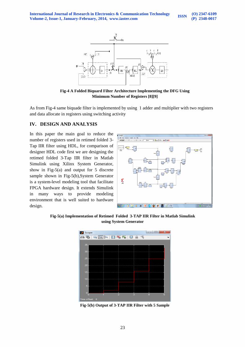
Fig-4 A Folded Biquard Filter Architecture Implementing the DFG Using
Minimum Number of Registers [8][9]
As from Fig-4 same biquade filter is implemented by using 1 adder and multiplier with two registers
and data allocate in registers using switching activity
IV. DESIGN AND ANALYSIS
In this paper the main goal to reduce the
number of registers used in retimed folded 3-
Tap IIR filter using HDL, for comparison of
designer HDL code first we are designing the
retimed folded 3-Tap IIR filter in Matlab
Simulink using Xilinx System Generator,
show in Fig-5(a) and output for 5 discrete
sample shown in Fig-5(b),System Generator
is a system-level modeling tool that facilitate
FPGA hardware design. It extends Simulink
in many ways to provide modeling
environment that is well suited to hardware
design.
Fig-5(a) Implementation of Retimed Folded 3-TAP IIR Filter in Matlab Simulink
using System Generator
Fig-5(b) Output of 3-TAP IIR Filter with 5 Sample

International Journal of Research in Electronics & Communication Technology
Volume-2, Issue-1, January-February, 2014, www.iaster.com ISSN
(O) 2347-6109
(P) 2348-0017
24
System Generator automatically compiles design into low-level representation. Design is compiled
and simulated using the System Generator. Automatically code is generated and code is synthesis in
Xilinx simulator to find number of register used in retimed folded 3-TAP IIR filter, Synthesis
report is been show in Fig-5(c).
Fig-5(c) Automatic Synthesis Report generated by System Generator
From the synthesis report the number of registers slice generated by System generator is 48, so our
aim to reduce number of Registers by writing HDL for folded structure. For folded structure we
need to do calculation analytically and by using matlab. The 3-tap IIR Filter been designed by using
dataflow graph .Dataflow graph gives detail information without implementation of hardware and
can be able to represent any algorithm. A DFG is a directed graph G(V,E) with a set of edges E.
These set of nodes V are subdivided into computational nodes, input and output nodes [1].
(a) (b)
Fig-6 (a) 3-TAP IIR filter (b) Dataflow graph of 3-TAP IIR filter
In dataflow graph representation the node represent computational time and directed edge represent
data path and each has a non-negative number of delay associated with node implementation of data
flow graph represent in Fig-7.This filter is folded with folding factor N=6,means that iteration period
of folded hardware is 4 U.T,each node in 3-tap IIR filter is executed exactly ones the iteration period
can be founded by using LPM(longest path matrix) and MCM(Minimum cycle mean) algorithm,
algorithm is implemented in matlab to check iteration period, after and before folding, the property of
folding transformation that loop bound and iteration bound should not change after adding number
of delay in path.
International Journal of Research in Electronics & Communication Technology
Volume-2, Issue-1, January-February, 2014, www.iaster.com ISSN
(O) 2347-6109
(P) 2348-0017
25
Fig-7 Dataflow Graph of 3-Tap IIR Filter Using Matlab
In present paper as per eqa-2 the weight (delay) of Df(UV) is calculated, some of edge may get
negative value shown in Table-8, the edge with negative Df(UV) can be made non-negative by
increasing (decreasing) number of delay the Df(UV) by Nw,while adding delay property should not
be effected.
Table-4 Folding Equation for Folding Constraint for DFG
Df(UV) Delay
112 -2
14 1
15 3
16 9
17 5
18 4
19 8
21 1
32 1
42 0
53 -1
63 -4
711 -5
810 -6
910 -4
1011 1
1112 2
In the Table-4 some of edge get negative value to make non-negative value, we added a
delay(register) to make them positive after adding delay to each negative value retime 3-TAP IIR
filter with valid folding retimed structure is shown in Fig-8,but adding delay there is increase in
latency but functionality and property
1.loop bound remain same
2.iteration bound must remain same
iteration bound and Loop bound of folded architecture can check by using LPM and MCM algorithm
shown in Fig-8(a),Fig-8(b).

International Journal of Research in Electronics & Communication Technology
Volume-2, Issue-1, January-February, 2014, www.iaster.com ISSN
(O) 2347-6109
(P) 2348-0017
26
Fig-8 Retimed 3-TAP IIR Filter with Valid Folding Architecture
Fig-8(a)Verified Iteration Bound using LPM after Adding Delay
Fig-8(B) Verified Iteration Bound using MCM after Adding Delay
International Journal of Research in Electronics & Communication Technology
Volume-2, Issue-1, January-February, 2014, www.iaster.com ISSN
(O) 2347-6109
(P) 2348-0017
27
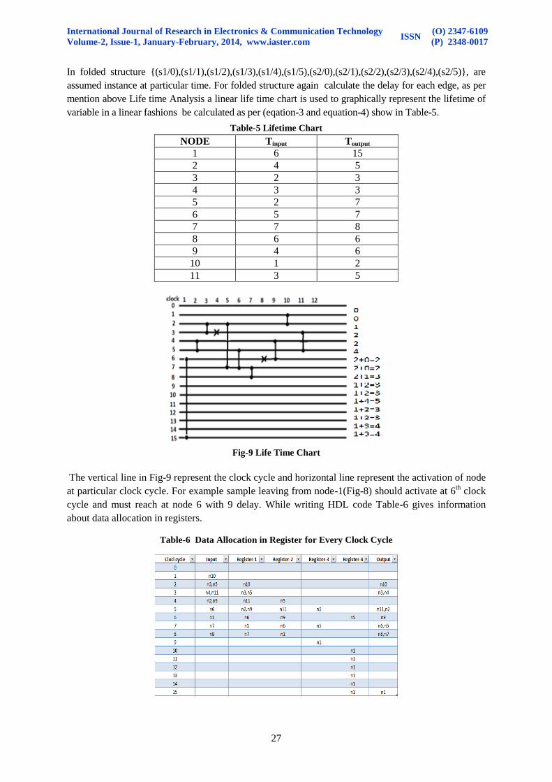
In folded structure {(s1/0),(s1/1),(s1/2),(s1/3),(s1/4),(s1/5),(s2/0),(s2/1),(s2/2),(s2/3),(s2/4),(s2/5)}, are
assumed instance at particular time. For folded structure again calculate the delay for each edge, as per
mention above Life time Analysis a linear life time chart is used to graphically represent the lifetime of
variable in a linear fashions be calculated as per (eqation-3 and equation-4) show in Table-5.
Table-5 Lifetime Chart
NODE Tinput Toutput
1 6 15
2 4 5
3 2 3
4 3 3
5 2 7
6 5 7
7 7 8
8 6 6
9 4 6
10 1 2
11 3 5
Fig-9 Life Time Chart
The vertical line in Fig-9 represent the clock cycle and horizontal line represent the activation of node
at particular clock cycle. For example sample leaving from node-1(Fig-8) should activate at 6th clock
cycle and must reach at node 6 with 9 delay. While writing HDL code Table-6 gives information
about data allocation in registers.
Table-6 Data Allocation in Register for Every Clock Cycle

International Journal of Research in Electronics & Communication Technology
Volume-2, Issue-1, January-February, 2014, www.iaster.com ISSN
(O) 2347-6109
(P) 2348-0017
28
Fig-10 Folded Architecture of 3-TAP IIR Filter Using Lifetime Chart
Fig-10 show is folded structure of 3-TAP IIR filter now to represent this structure in digital design for
writing HDL we need to replace those switches by multiplexer and need RAM to store data for filter
co-efficient and to store
Multiplier output which can be further used Fig-11 show the implementation of Fig-10(Folded
architecture of 3-TAP IIR filter) in digital design.
Fig-11 3-TAP IIR Filter Folded Digital Design
3-TAP IIR filter with folded structure using 4 register,1 adder and 1 multiplier in Xilinx with HDL
code and synthesis and design summary report is to be compare the result with report generated by
System Generator
V. SIMULATION RESULT
Fig-12 3-tap IIR Folded Filter using Xilinx Simulation Tool
International Journal of Research in Electronics & Communication Technology
Volume-2, Issue-1, January-February, 2014, www.iaster.com ISSN
(O) 2347-6109
(P) 2348-0017
29
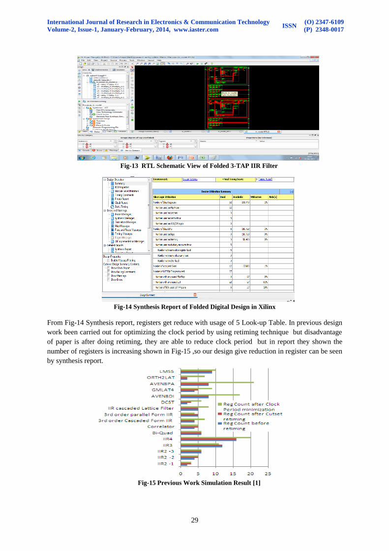
Fig-13 RTL Schematic View of Folded 3-TAP IIR Filter
Fig-14 Synthesis Report of Folded Digital Design in Xilinx
From Fig-14 Synthesis report, registers get reduce with usage of 5 Look-up Table. In previous design
work been carried out for optimizing the clock period by using retiming technique but disadvantage
of paper is after doing retiming, they are able to reduce clock period but in report they shown the
number of registers is increasing shown in Fig-15 ,so our design give reduction in register can be seen
by synthesis report.
Fig-15 Previous Work Simulation Result [1]

International Journal of Research in Electronics & Communication Technology
Volume-2, Issue-1, January-February, 2014, www.iaster.com ISSN
(O) 2347-6109
(P) 2348-0017
30
VI. CONCLUSION
In this particular work a design optimized platform is developed for Digital filter. There are two ways
by which optimization is performed in the current work. Firstly folding and second lifetime analysis
technique but in folding functional unit and critical path is reduced but there is increasing in number
of registers so lifetime analysis method is chosen which reduce the critical path, functional unit as
well as registers and generates the synthesizable HDL. Since the entire process is reduce area
occupied by register.
VII. REFERENCES
[1] Deepa Yagain,Dr. Vijaya Krishna A"Design Optimization Platform for Synthesizable High
Speed Digital Filters Using Retiming Technique"IEEE-ICSE2012 Proc., 2012, Kuala Lumpur,
Malaysia.
[2] Daniel D. Gajski, Lognath Ramachandran “IEEE Design & Test,” volume 11, Issue 4 (Oct
1994), Publishers: IEEE computer society press, Los Alamitos, CA,USA ,ISSN: 0740-7475,pp-
44-54.
[3] Zahra Jeddi and Esmail Amini “Power optimization of Sequential Circuits by Retiming and
Rewiring”, IEEE, 2006
[4] Ozgur Sinanoglu and Vishwani D. Agrawal “Retiming Scan Circuit to Eliminate Timing
Penalty”,IEEE, 2010.
[5] A. Chandrakasan, S. Sheng, and R. Brodersen, “Low-power CMOS digital design,” IEEE J.
Solid-State Circuits, vol. 27, pp. 473–484, Apr. 1992.
[6] Zahra Jeddi and Esmail Amini ”Power optimization of Sequential Circuits by Retiming and
Rewiring”, IEEE, 2006.
[7] K. K. Parhi "Synthesis of Control Circuits in Folded Pipelined DSP Architectures", IEEE Jl. of
Solid-State Circuits, vol. SC-27, no. 1, pp.29 -43 1992.
[8] KESHAB K.PARHI "VLSI DIGITAL SIGNAL PROCESSING SYSTEM design and
implementation" ISBN:978-81-265-1098-6, 2012.
[9] Pierre COULON "Postgraduate Course on Signal Processing in Communications, FALL – 99.
[10] S. Srinivasan. "A novel architecture for lifting-based discrete wavelet transform for
JPEG2000standard suitable for VLSI implementation", 16th International Conference on VLSI
Design2003 Proceedings ICVD-03, 2003.