organic electronics on banknotes - max planck society · pdf filemodern banknotes include up...
TRANSCRIPT

www.advmat.dewww.MaterialsViews.com
CO
MM
UN
ICATI
ON
654
Organic Electronics on Banknotes
Ute Zschieschang , * Tatsuya Yamamoto , Kazuo Takimiya , Hirokazu Kuwabara , Masaaki Ikeda , Tsuyoshi Sekitani , Takao Someya , and Hagen KlaukModern banknotes include up to 50 different anti-counterfeiting features, such as watermarks, holograms, raised printing, embedded foil strips, fl uorescent inks, and many others. To supplement these passive security features, active electronic anti-counterfeiting and tracking features in the form of silicon integrated circuits have been considered, [ 1 ] but have thus far not been realized, mainly because of the signifi cant thickness of standard silicon wafers ( > 500 μ m). The thickness of silicon chips can be reduced to about 20 μ m, [ 2 , 3 ] but this may still be too thick for incorporation into banknotes. Other techniques allow thin silicon membranes to be transferred from a wafer onto plastic substrates and be processed into fl exible circuits. [ 4 , 5 ] Although it may be possible to transfer silicon membranes onto banknotes as well, the harsh process conditions during circuit fabrication following the transfer of the membranes may irre-versibly damage the banknotes.
In contrast, organic thin-fi lm transistors (TFTs) are readily fabricated on a variety of surfaces, including foils, [ 6 − 10 ] fi bers, [ 11 , 12 ] and paper. [ 13–15 ] The ability to fabricate organic cir-cuits on banknotes may create the possibility of outfi tting ban-knotes with active electronic security features, provided the device fabrication process does not damage the banknotes and provided the operating voltage and power consumption of the circuits is suffi ciently low to allow power being supplied by radio-frequency coupling with low magnetic fi elds. [ 16 ]
The key to realizing low-voltage organic TFTs on delicate substrates, such as banknotes, is the use of a high-capacitance gate dielectric prepared under mild thermal and chemical con-ditions. A promising option are hybrid dielectrics composed of a thin aluminum oxide layer and an alkylphosphonic acid
© 2011 WILEY-VCH Verlag Gmwileyonlinelibrary.com
Dr. U. Zschieschang , Dr. H. Klauk Max Planck Institute for Solid State Research Heisenbergstr. 1, 70569 Stuttgart, Germany E-mail: [email protected] Dr. T. Yamamoto , Prof. K. Takimiya Department of Applied Chemistry Graduate School of EngineeringInstitute for Advanced Materials ResearchHiroshima UniversityHigashi-Hiroshima, Japan Dr. H. Kuwabara , Dr. M. Ikeda Functional Chemicals R&D Laboratories Nippon Kayaku Co., Ltd., Kita-ku, Tokyo, Japan Prof. T. Sekitani , Prof. T. Someya Department of Electrical EngineeringUniversity of TokyoTokyo, Japan
DOI: 10.1002/adma.201003374
self-assembled monolayer (SAM). [ 17 − 19 ] The aluminum oxide layer is produced by briefl y exposing the surface of the alu-minum gate electrodes (bottom-gate structure) to an oxygen plasma, which increases the native AlO x thickness to about 3 to 4 nm, depending on the plasma power. The organic mono-layer is then allowed to self-assemble on the AlO x surface by immersing the substrate in a solution of a commercially avail-able alkylphosphonic acid in a gentle solvent (2-propanol). Anchoring of the alkylphosphonic acid molecules on the AlO x surface occurs by heterocondensation of the phosphonic acid groups with surface hydroxyl groups [ 20 ] and involves the for-mation of mono-, bi-, or tridentate adsorption complexes (with the phosphonic acid group binding to the surface via one, two, or three P-O-Al linkages). [ 21–23 ] Mono- or bidentate surface binding would also allow the unreacted phosphonic-acid moi-eties to crosslink with adjacent molecules. One concern with AlO x /SAM dielectrics is whether the AlO x surface might be cor-roded by the alkylphosphonic acid. Corrosion has indeed been observed when using phosphonic acids with very short alkyl chain lengths, such as ethylphosphonic acid, [ 19 ] but has not been observed with long-chain phosphonic acids, such as octa-decylphosphonic acid, which is employed in this work.
AlO x /SAM gate dielectrics have previously been used to fab-ricate low-voltage organic complementary circuits on glass [ 24 ] and on plastic substrates [ 25 ] and are utilized in this work to realize functional organic TFTs and circuits on banknotes. The transistors and circuits have a thickness of less than 250 nm and can be operated with voltages of about 3 V.
A photograph of a 5-Euro note with arrays of organic TFTs and circuits fabricated directly on the surface of the banknote is shown in Figure 1 a . The fabrication process (described in the Supporting Information) is similar to the process previously reported for the fabrication of low-voltage organic TFTs and cir-cuits on glass. [ 17 ] Except for the formation of the SAM, this is an all-dry manufacturing process that avoids the use of liquids and chemicals. The organic semiconductors, dinaphtho[2,3-b:2 ′ ,3 ′ -f ]thieno[3,2-b]thiophene (DNTT) [ 26 , 27 ] for the p-channel TFTs and hexadecafl uorocopperphthalocyanine (F 16 CuPc) [ 28 ] for the n-channel TFTs, were both deposited in vacuum. The TFTs employ the inverted staggered (bottom-gate, top-contact) device structure. The metal and semiconductor layers were all patterned using polymer shadow masks. [ 24–27 ] Mechanical and environmental protection of the TFTs and circuits is in prin-ciple possible by covering the devices with a thin organic/metallic passivation layer deposited at room temperature from the vapor phase. [ 29 ]
Figure 1 illustrates the signifi cant surface topography of the banknotes. However, because the topography is dominated by long-range waviness, rather than short-range roughness,
bH & Co. KGaA, Weinheim Adv. Mater. 2011, 23, 654–658

www.advmat.dewww.MaterialsViews.com
CO
MM
UN
ICATIO
N
Figure 1 . a) Photograph of a 5-Euro note with arrays of organic transis-tors and circuits. b) Photograph of an individual transistor on a banknote (image acquired with a Keyence VHX-1000 microscope). c) Cross-sectional scanning electron microscopy (SEM) image of the surface of a banknote with an Al/AlO x /SAM/Au capacitor. d) Transmission elec-tron microscopy (TEM) image of the surface of a banknote with an Al/AlO x /SAM/Au capacitor (image acquired with an HF-3300 Cold-FE TEM, Hitachi High-Technologies Corp.).
it is possible to obtain organic TFTs with acceptable electrical performance despite this topography. Figure 2 shows the
Figure 2 . a) Current-voltage characteristics of a DNTT p-channel transistor on a 5-Euro note. The fi eld-effect mobility is 0.2 cm 2 V − 1 s − 1 . b) Current-voltage characteristics of a F 16 CuPc n-channel transistor on a 5-Euro note. The fi eld-effect mobility is 0.005 cm 2 V − 1 s − 1 .
current-voltage characteristics of a DNTT p-channel TFT and of a F 16 CuPc n-channel TFT on a 5-Euro note. Owing to the small thickness (5.7 nm) and the large capaci-tance (700 nF cm − 2 ) of the AlO x /SAM gate dielectric, the TFTs can be operated with low voltages of about 3 V. Despite the small dielectric thickness, the gate leakage cur-rent at the maximum gate bias is below 10 − 9 A, confi rming that the plasma-grown AlO x and the solution-processed alkylphosphonic acid SAM form a continuous, conformal coating with useful insulating properties on the aluminum gate electrodes. The fi eld-effect mobility extracted from the transfer characteristics of the DNTT p-channel TFT is 0.2 cm 2 V − 1 s − 1 , which is within a factor of three of the mobility of DNTT TFTs on plastic substrates [ 27 ] and within an order of magnitude of the mobility on oxidized sil-icon substrates. [ 26 ] The subthreshold swing is 110 mV per decade, which is close to that of DNTT TFTs on plastic substrates (100 mV decade − 1 ). [ 27 ] The mobility of the F 16 CuPc n-channel TFTs (0.005 cm 2 V − 1 s − 1 ) is within a factor of 5 of that of F 16 CuPc TFTs on glass. [ 17 , 18 , 28 ]
The shortest channel length we are able to realize with polymer shadow masks is 10 μ m. A comparison of DNTT TFTs with
© 2011 WILEY-VCH Verlag GmAdv. Mater. 2011, 23, 654–658
channel lengths of 10, 15, and 30 μ m on a 5-Euro note is shown in Figure S4. The mobility of these TFTs is essentially inde-pendent of the channel length (0.2 cm 2 V − 1 s − 1 ). The shorter TFTs have a larger off-state drain current (10 − 10 rather than 10 − 11 A) and hence a smaller on/off ratio (10 4 rather than 10 5 ) than the long-channel devices. For comparison, DNTT TFTs on plastic substrates have off-state drain currents of about 10 − 12 A and on/off ratios of about 10 6 . [ 22 ]
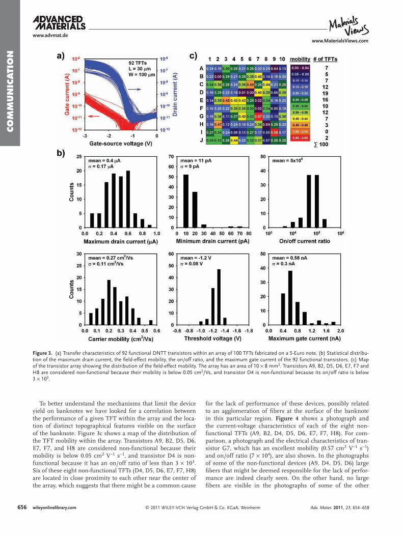
To evaluate the yield and uniformity of organic TFTs on banknotes we measured 100 DNTT transistors with identical channel length (30 μ m) and channel width (100 μ m) on a 5-Euro note. If we defi ne a TFT as functional if the mobility is at least 0.05 cm 2 V − 1 s − 1 and the on/off ratio is at least 3 × 10 3 , then the yield is 92%. The current-voltage characteristics and the distribution of the electrical parameters of these 92 functional TFTs are shown in Figure 3 a and 3 b . Compared with organic TFTs on glass substrates, where the yield is essentially 100% and the parameter variations are only a few percent, [ 17 ] the yield we have obtained on banknotes is substantially lower and the parameter distribution is substantially wider. The threshold voltage, for example, has a standard deviation of 80 mV and varies between −1.0 and −1.4 V (see Figure 3b ). Such wide parameter variations would be problematic if the TFTs were employed in active-matrix light-emitting diode displays or in analog or mixed-signal integrated circuits, where image fi delity and circuit linearity are strongly dependent on tight parameter uniformity. [ 24 ] Properly designed digital circuits, on the other hand, can often tolerate a certain level of parameter variations. [ 30 ]
655bH & Co. KGaA, Weinheim wileyonlinelibrary.com 655
www.advmat.dewww.MaterialsViews.com
CO
MM
UN
ICATI
ON
656
Figure 3 . (a) Transfer characteristics of 92 functional DNTT transistors within an array of 100 TFTs fabricated on a 5-Euro note. (b) Statistical distribu-tion of the maximum drain current, the fi eld-effect mobility, the on/off ratio, and the maximum gate current of the 92 functional transistors. (c) Map of the transistor array showing the distribution of the fi eld-effect mobility. The array has an area of 10 × 8 mm 2 . Transistors A9, B2, D5, D6, E7, F7 and H8 are considered non-functional because their mobility is below 0.05 cm 2 /Vs, and transistor D4 is non-functional because its on/off ratio is below 3 × 10 3 .
To better understand the mechanisms that limit the device yield on banknotes we have looked for a correlation between the performance of a given TFT within the array and the loca-tion of distinct topographical features visible on the surface of the banknote. Figure 3c shows a map of the distribution of the TFT mobility within the array. Transistors A9, B2, D5, D6, E7, F7, and H8 are considered non-functional because their mobility is below 0.05 cm 2 V − 1 s − 1 , and transistor D4 is non-functional because it has an on/off ratio of less than 3 × 10 3 . Six of these eight non-functional TFTs (D4, D5, D6, E7, F7, H8) are located in close proximity to each other near the center of the array, which suggests that there might be a common cause
© 2011 WILEY-VCH Verlag Gmwileyonlinelibrary.com
for the lack of performance of these devices, possibly related to an agglomeration of fi bers at the surface of the banknote in this particular region. Figure 4 shows a photograph and the current-voltage characteristics of each of the eight non-functional TFTs (A9, B2, D4, D5, D6, E7, F7, H8). For com-parison, a photograph and the electrical characteristics of tran-sistor G7, which has an excellent mobility (0.57 cm 2 V − 1 s − 1 ) and on/off ratio (7 × 10 4 ), are also shown. In the photographs of some of the non-functional devices (A9, D4, D5, D6) large fi bers that might be deemed responsible for the lack of perfor-mance are indeed clearly seen. On the other hand, no large fi bers are visible in the photographs of some of the other
bH & Co. KGaA, Weinheim Adv. Mater. 2011, 23, 654–658

www.advmat.dewww.MaterialsViews.com
CO
MM
UN
ICATIO
N
© 2011 WILEY-VCH Verlag GmbH & Co. KGaA, WeinheimAdv. Mater. 2011, 23, 654–658
Figure 4 . Photographs and current-voltage characteristics of eight non-functional transistors (A9, B2, D4, D5, D6, E7, F7, H8) and one functional transistor (G7) out of 100 DNTT transistors on a 5-Euro note. A clear correlation between the presence of large fi bers and the transistor performance is not apparent.
non-functional TFTs (F7, H8). Interestingly, the photograph of the high-performance transistor (G7) clearly shows several large fi bers, which apparently have no detri-mental effect on the electrical performance of this device. Thus, a clear correlation between surface topography and TFT per-formance is not immediately apparent.
In order to assess the dynamic per-formance of organic TFTs on banknotes we fabricated unipolar inverters con-sisting of two DNTT TFTs (one acting as a drive transistor, the other as a saturated load device; see Figure S6). When oper-ated with a supply voltage of 3 V, these inverters are capable of switching digital signals at frequencies of up to about 2 kHz (see Figure S6). This frequency is several orders of magnitude higher than the oper-ating frequency previously reported for organic TFTs on paper [ 13 , 14 ] and is within an order of magnitude of the frequency of low-voltage organic TFTs on plastic substrates. [ 27 ]
Frequencies of a few kilohertz may already be suffi cient for basic logic opera-tions. However, as Figure S6 indicates, the small-signal gain, the output swing, and the noise margins of the unipolar circuits are quite small, which may lead to prob-lems with the signal integrity in circuits of greater complexity. [ 30 ] Also, unipolar circuits have a relatively large static power consumption, since the load transistor is always conducting. These drawbacks are eliminated in complementary circuits, which employ p-channel and n-channel transistors. [ 31 ] Figure 5 shows a photo-graph and the static transfer character-istics of a complementary inverter com-prised of a F 16 CuPc n-channel TFT and a DNTT p-channel TFT on a 5-Euro note. The static characteristics of these comple-mentary inverters (supply voltage about 3 V, static power consumption < 1 nW, small-signal gain about 100) are compa-rable to those of silicon complementary circuits fabricated on silicon membranes and transferred from a silicon wafer onto a fl exible plastic substrate. [ 4 ] The maximum operating frequency of the organic complementary circuits is limited to a few hundred Hertz by the relatively small fi eld-effect mobility of the F 16 CuPc n-channel TFTs (see Figure S7). However, operating frequencies in the range of a few kilohertz are feasible by employing conju-gated organic semiconductors with larger electron mobilities. [ 32–34 ]
657wileyonlinelibrary.com 657

www.advmat.dewww.MaterialsViews.com
CO
MM
UN
ICATI
ON
658
Figure 5 . Circuit schematic, photograph, and static transfer characteris-tics of an organic complementary inverter on a 5-Euro note.
[ [ [ [
[
[
[
[
[ [
[ [ [
[
[
[
[ [
[ [
[
[
[
[
[
[ 1 ] J. Yoshida , Integrating Touch Interfaces , EE Times , 19 December 2001 (available at http://www.eetimes.com/story/OEG20011219S0016).
[ 2 ] M. Zimmermann , J. N. Burghartz , W. Appel , N. Remmers , C. A. Burwick , IEEE International Electron Devices Meeting Technical Digest 2006 , 1010 .
[ 3 ] H. Rempp , J. Burghartz , C. Harendt , N. Pricopi , M. Pritschow , C. Reuter , H. Richter , I. Schindler , M. Zimmermann , IEEE Interna-tional Solid State Circuits Conference Technical Digest 2008 , 334 .
[ 4 ] D. H. Kim , J.-H. Ahn , W. M. Choi , H.-S. Kim , T.-H. Kim , J. Song , Y. Y. Huang , Z. Liu , C. Lu , J. A. Rogers , Science 2008 , 320 , 507 .
[ 5 ] H. C. Yuan , G. K. Celler , Z. Ma , J. Appl. Phys. 2007 , 102 , 034501 . [ 6 ] J. A. Rogers , Z. Bao , K. Baldwin , A. Dodabalapur , B. Crone ,
V. R. Raju , V. Kuck , H. Katz , K. Amundson , J. Ewing , P. Drzaic , Proc. Natl. Acad. Sci. USA 2001 , 98 , 4835 .
Supporting Information Supporting Information is available from the Wiley Online Library or from the author.
Acknowledgements The authors thank Benjamin Stuhlhofer at the Max Planck Institute for Solid-State Research for expert technical assistance and Richard Rook at CADiLAC Laser for providing high-quality polymer shadow masks. We gratefully acknowledge the fi nancial support provided by the New Energy and Industrial Technology Development Organization (NEDO) of Japan.
Received: September 16, 2010 Revised: November 1, 2010
Published online: December 6, 2010
© 2011 WILEY-VCH Verlag Gmwileyonlinelibrary.com
[ 7 ] G. H. Gelinck , H. E. A. Huitema , E. van Veenendaal , E. Cantatore , L. Schrijnemakers , J. B. P. H. Van Der Putten , T. C. T. Geuns , M. Beenhakkers , J. B. Giesbers , B. H. Huisman , E. J. Meijer , E. M. Benito , F. J. Touwslager , A. W. Marsman , B. J. E. van Rens , D. M. de Leeuw , Nat. Mater. 2004 , 3 , 106 .
[ 8 ] L. Zhou , A. Wanga , S. C. Wu , J. Sun , S. Park , T. N. Jackson , Appl. Phys. Lett. 2006 , 88 , 083502 .
[ 9 ] T. Sekitani , M. Takamiya , Y. Noguchi , S. Nakano , Y. Kato , T. Sakurai , T. Someya , Nat. Mater. 2007 , 6 , 413 .
10 ] C. J. Bettinger , Z. Bao , Adv. Mater. 2010 , 22 , 651 . 11 ] J. Granstrom , H. E. Katz , J. Mater. Res. 2004 , 19 , 3540 . 12 ] J. Lee , V. Subramanian , IEEE Trans. Electron Devices 2005 , 52 , 269 . 13 ] P. Andersson , D. Nilsson , P. O. Svensson , M. Chen , A. Malmström ,
T. Remonen , T. Kugler , M. Berggren , Adv. Mater. 2002 , 14 , 1460 . 14 ] F. Eder , H. Klauk , M. Halik , U. Zschieschang , G. Schmid , C. Dehm ,
Appl. Phys. Lett. 2004 , 84 , 2673 . 15 ] Y. H. Kim , D. G. Moon , J. I. Han , IEEE Electron Device Lett. 2004 , 25 ,
702 . 16 ] K. Myny , S. Steudel , S. Smout , P. Vicca , F. Furthner ,
B. Van Der Putten , A. K. Tripathi , G. H. Gelinck , J. Genoe , W. Dehaene , P. Heremans , Org. Electron. 2010 , 11 , 1176 .
17 ] H. Klauk , U. Zschieschang , J. Pfl aum , M. Halik , Nature 2007 , 445 , 745 .
18 ] U. Zschieschang , M. Halik , H. Klauk , Langmuir 2008 , 24 , 1665 . 19 ] A. Jedaa , M. Burkhardt , U. Zschieschang , H. Klauk , D. Habich ,
G. Schmid , M. Halik , Org. Electronics 2009 , 10 , 1442 . 20 ] H. Y. Nie , Anal. Chem. 2010 , 82 , 3371 . 21 ] P. H. Mutin , G. Guerrero , A. Vioux , J. Mater. Chem. 2005 , 15 , 3761 . 22 ] M. J. Pellerite , T. D. Dunbar , L. D. Boardman , E. J. Wood , J. Phys.
Chem. B 2003 , 107 , 11726 . 23 ] R. Luschtinetz , A. F. Oliveira , H. A. Duarte , G. Seifer , Z. Anorg. Allg.
Chem. 2010 , 636 , 1506 24 ] W. Xiong , Y. Guo , U. Zschieschang , H. Klauk , B. Murmann , IEEE J.
Solid-State Circuits 2010 , 45 , 1380 . 25 ] K. Ishida , N. Masunaga , Z. Zhou , T. Yasufuku , T. Sekitani ,
U. Zschieschang , H. Klauk , M. Takimiya , T. Someya , T. Sakurai , IEEE J. Solid-State Circuits 2010 , 45 , 249 .
26 ] T. Yamamoto , K. Takimiya , J. Am. Chem. Soc. 2007 , 129 , 2224 . 27 ] U. Zschieschang , F. Ante , T. Yamamoto , K. Takimiya , H. Kuwabara ,
M. Ikeda , T. Sekitani , T. Someya , K. Kern , H. Klauk , Adv. Mater. 2010 , 22 , 982 .
28 ] M. M. Ling , Z. Bao , Org. Electron. 2006 , 7 , 568 . 29 ] T. Sekitani , H. Nakajima , H. Maeda , T. Fukushima , T. Aida , K. Hata ,
T. Someya , Nat. Mater. 2009 , 8 , 494 . 30 ] D. Bode C. Rolin , S. Schols , M. Debucquoy , S. Steudel , G. H. Gelinck ,
J. Genoe , P. Heremans , IEEE Trans. Electron Devices 2010 , 57 , 201 . 31 ] B. K. Crone , A. Dodabalapur , R. Sarpeshkar , R. W. Filas , Y. Y. Lin ,
Z. Bao , J. H. O’Neill , W. Li , H. E. Katz , J. Appl. Phys. 2001 , 89 , 5125 .
32 ] H. Yan , Z. Chen , Y. Zheng , C. Newman , J. R. Quinn , F. Dötz , M. Kastler , A. Facchetti , Nature 2009 , 457 , 679 .
33 ] R. Schmidt , J. H. Oh , Y. S. Sun , M. Deppisch , A. M. Krause , K. Radacki , H. Braunschweig , M. Könemann , P. Erk , Z. Bao , F. Würthner , J. Am. Chem. Soc. 2009 , 131 , 6215 .
34 ] J. H. Oh , S. L. Suraru , W. Y. Lee , M. Könemann , H. W. Höffken , C. Röger , R. Schmidt , Y. Chung , W. C. Chen , F. Würthner , Z. Bao , Adv. Funct. Mater. 2010 , 20 , 2148 .
bH & Co. KGaA, Weinheim Adv. Mater. 2011, 23, 654–658

Supporting Information
Organic Electronics on Banknotes
By Ute Zschieschang, Tatsuya Yamamoto, Kazuo Takimiya,
Hirokazu Kuwabara, Masaaki Ikeda, Tsuyoshi Sekitani, Takao Someya,
and Hagen Klauk 1. Device Fabrication Process
The organic TFTs employ the inverted staggered (bottom-gate, top-contact) device structure and are fabricated directly on the surface of the banknotes (see Figure S1).
In the first step of the device process, the gate electrodes of the TFTs are defined by evaporating 70 nm thick aluminum through a polymer shadow mask (CADiLAC Laser, Hilpoltstein, Germany).
To create access to the gate electrodes, 50 nm thick gold is then evaporated through a second shadow mask in specific areas on the aluminum.
To form the gate dielectric, the banknote is then exposed to an oxygen plasma for a few seconds (plasma power: 150 W, duration: 15 s; increases the thickness of the native AlOx layer from ~1.5 to 3.6 nm) and then immersed in a 2-propanol solution of n-octadecylphosphonic acid (from PCI Synthesis) for about one hour (results in a 2.1 nm thick SAM on the AlOx surface).
50 nm of hexadecafluorocopperphthalocyanine (F16CuPc; from Sigma Aldrich) and dinaphtho[2,3-b:2’,3’-f]thieno[3,2-b]thiophene (DNTT) are then deposited in vacuum through a third and fourth shadow mask as the organic semiconductors for
the n-channel and p-channel TFTs. During the semiconductor depositions the banknote is held at temperatures of 90 °C for the F16CuPc and 60 °C for the DNTT deposition, since this was found to give the best device performance.
TFTs and circuits are completed by evaporating 100 nm thick gold through a fifth shadow mask to define the source and drain contacts.
Except for the formation of the phosphonic acid SAM, this is an all-dry manufacturing process. The highest process temperature is 90 ºC. During the depositions, the banknote is always covered by a shadow mask, so the materials are deposited only where needed for the devices, and no processing is required to pattern the films or remove excess material. The formation of the AlOx is specific to the aluminum surfaces, and the formation of the SAM is specific to the plasma-generated AlOx surfaces, so these two materials also do not require post-growth patterning. Neither the oxygen-plasma exposure to form the thin AlOx layer, nor the exposure to 2-propanol for the formation of the self-assembled monolayer, nor heating to 90 ºC during the semiconductor deposition cause any detectable damage to the banknotes.
S
S
N
N
N
N
N
N
N
N
Cu
F
F
F
F
F
F
F FF
F
F
FFF
F
F
Banknote
Source Drain
Al gate electrode
AlOx/SAM gate dielectricOrganic semiconductor
Figure S1. Left: Schematic cross-section of the organic thin-film transistors (TFTs). Center: Hexadecafluorocopperphthalocyanine (F16CuPc), the semiconductor for the n-channel TFTs. Right: Dinaphtho[2,3-b:2’,3’-f]thieno[3,2-b]thiophene (DNTT), the semiconductor for the p-channel TFTs.
1

2. Electrical Characterization
All of the electrical measurements are performed in ambient air at room temperature under weak yellow laboratory light.
3. Microscopy Images
Figure S2 and Figure S3 show atomic force microscopy (AFM), cross-sectional scanning electron microscopy (SEM), and cross-sectional transmission electron microscopy (TEM) images of the surface of a banknote (The latter two are also shown in Figure 1 and are reproduced here for better clarity.)
Figure S2. Atomic force microscopy (AFM) image of the surface of a banknote.
Figure S3. Cross-sectional scanning electron microscopy (SEM; left) and transmission electron microscopy (TEM; right) images of the surface of a banknote with an Al/AlOx/SAM/Au capacitor.
2

4. Lateral Transistor Dimensions
The maximum frequency fT at which a field-effect transistor can be operated is determined by its transconductance gm and gate capacitance Cgate:
gate
mT C2
gf
where
L
VWC
V
Ig DSdiel
GS
Dm
and LLWCC dielgate
so that
where ID is the drain current, VGS and VDS are the gate-source and drain-source voltage, µ is the carrier mobility, W is the channel width, and Cdiel is the gate dielectric capacitance per unit area (here: Cdiel = 700 nF/cm2).
It can be seen that transistor operation at high frequencies requires a small channel length (L) and gate-to-contact overlap (L). Figure S4 shows photographs and electrical characteristics of DNTT transistors on a 5-Euro note with channel length and gate to source overlap ranging from 30 µm to 10 µm. All TFTs were patterned using manually aligned polymer shadow masks.
LLL2
Vf DS
T
(1)
According to Equation (1), TFTs with channel length and gate overlap of 10 µm has a maximum frequency fT of about 10 kHz.
L = L = 30 µm
Gate-source voltage (V)
-2 -1 0
Ho
le m
ob
ility
(cm
2 /Vs)
0.0
0.1
0.2
0.3Drain-source voltage = -1.5 V
Gate-source voltage (V)
-3 -2 -1 0
Gat
e c
urr
en
t (A
)
10-12
10-11
10-10
10-9
10-8
10-7
10-6
Dra
in c
urr
ent
(A)
10-12
10-11
10-10
10-9
10-8
10-7
10-6
Drain-source voltage = -1.5 V
Drain-source voltage (V)
-3 -2 -1 0
Dra
in c
urr
ent
(A
)
-0.6
-0.4
-0.2
0.0
Gate-source voltage = -3.0 V
-1.8 V
-2.1 V
-2.4 V
-2.7 V
-1.5 V
L = L = 15 µm
Gate-source voltage (V)-2 -1 0
Ho
le m
ob
ility
(cm
2/V
s)
0.0
0.1
0.2
0.3Drain-source voltage = -1.5 V
Drain-source voltage (V)
-3 -2 -1 0
Dra
in c
urr
ent
(A
)
-1.2
-0.9
-0.6
-0.3
0.0
Gate-source voltage = -3.0 V
-1.8 V
-2.1 V
-2.4 V
-2.7 V
Gate-source voltage (V)
-3 -2 -1 0
Ga
te c
urr
en
t (A
)
10-12
10-11
10-10
10-9
10-8
10-7
10-6
Dra
in c
urr
en
t (A
)
10-12
10-11
10-10
10-9
10-8
10-7
10-6Drain-source voltage = -1.5 V
L = L = 10 µm
Gate-source voltage (V)-2 -1 0
Ho
le m
ob
ility
(cm
2/V
s)
0.0
0.1
0.2
0.3Drain-source voltage = -1.5 V
Gate-source voltage (V)
-3 -2 -1 0
Ga
te c
urr
en
t (A
)
10-12
10-11
10-10
10-9
10-8
10-7
10-6
10-5
Dra
in c
urr
en
t (A
)
10-12
10-11
10-10
10-9
10-8
10-7
10-6
10-5
Drain-source voltage = -1.5 V
Drain-source voltage (V)
-3 -2 -1 0
Dra
in c
urr
ent
(A
)
-2.0
-1.5
-1.0
-0.5
0.0
Gate-source voltage = -3.0 V
-1.8 V
-2.1 V
-2.4 V
-2.7 V
Figure S4. Current-voltage characteristics of DNTT TFTs with a channel length and a gate-to-contact overlap of 30 µm, 15 µm and 10 µm on a 5-Euro note. All three TFTs have a channel width of 100 µm. The carrier field-effect mobility is between 0.2 and 0.3 cm2/Vs for all three TFTs.
3

Figure S5. Transfer characteristics of a DNTT TFT with a channel length of 30 µm and a channel width of 100 µm on a 5-Euro note measured immediately after fabrication (“fresh”) and measured again after the banknote had been exposed to air at room temperature for 64 days. As can bee seen, the carrier mobility has decreased only slightly, from 0.28 to 0.21 cm2/Vs, while the on/off ratio has decreased from 5×10⁴ to3×104. This confirms the excellent air-stability of dinaphtho[2,3-b:2’,3’-f]thieno[3,2-b]thiophene.
Gate-source voltage (V)
-3 -2 -1 0
Gat
e cu
rren
t (A
)
10-12
10-11
10-10
10-9
10-8
10-7
10-6
Dra
in c
urr
en
t (A
)
10-12
10-11
10-10
10-9
10-8
10-7
10-6
Drain-source voltage = -1.5 V
fresh(0.28 cm2/Vs)
fresh
after64 days
in air(0.21 cm2/Vs)
after64 days
in air
Ou
tpu
t v
olt
ag
e (
V)
-2.0
-1.5
-1.0
-0.5
0.0
Cu
rren
t (A
)
10-10
10-9
10-8
10-7
10-6
10-5
10-4
Input voltage (V)
-3 -2 -1 0
Ga
in
0
1
2
VDD = -3 V
Figure S6. Circuit schematic, photograph, static voltage transfer characteristics, and dynamic switching characteristics of an organic unipolar inverter based on DNTT p-channel TFTs on a 5-Euro note. The inverter shows the correct logic function and responds to input signals with a frequency of a few kilohertz.
p-channel TFT
VDD
output p-channel TFT
input
Drain-source voltage (V)
0 1 2 3
Dra
in c
urr
ent
(nA
)
0
20
40
60
80
100Gate-source voltage = 2.1 V
1.5 V
1.2 V
1.8 V
0.9 V
Gate-source voltage (V)
-1 0 1
Ele
ctro
n m
ob
ility
(cm
2/V
s)
0.000
0.001
0.002
0.003
0.004
0.005
0.006Drain-source voltage = 1.5 V
Gate-source voltage (V)
-1 0 1 2
Dra
in c
urr
ent
(A)
10-12
10-11
10-10
10-9
10-8
10-7
Gat
e cu
rren
t (A
)
10-12
10-11
10-10
10-9
10-8
10-7
Drain-source voltage = 1.5 V
p-channel TFT
VDD
input output
n-channel TFT
Figure S7. Top: Current-voltage characteristics of an F16CuPc n-channel TFT on a 5-Euro note. Bottom: Circuit schematic, microscope photograph, and dynamic switching characteristics of a complementary inverter based on organic p-channel and n-channel TFTs on a 5-Euro note. The inverter shows the correct logic function (see Figure 5) and responds to input signals with a frequency of a few hundred Hertz.
4

Figure S8. Organic TFTs have also been fabricated on US-dollar, Swiss-franc and Japanese-yen notes. This figure shows the electrical characteristics of p-channel TFTs with a channel length of 30 µm and a channel width of 100 µm using pentacene as the semiconductor. The carrier mobility of these TFTs is between 0.01 and 0.02 cm2/Vs, and the on/off ratio is between 103 and 104.
Drain-source voltage (V)
-2 -1 0
Dra
in c
urr
en
t (n
A)
-15
-10
-5
0
Gate-source voltage = -3.0 V
-1.8 V
-2.1 V
-2.4 V
-2.7 V
Drain-source voltage (V)
-2 -1 0
Dra
in c
urr
ent
(nA
)
-40
-30
-20
-10
0
Gate-source voltage = -3.0 V
-1.8 V
-2.1 V
-2.4 V
-2.7 V
Drain-source voltage (V)
-2 -1 0
Dra
in c
urr
en
t (n
A)
-30
-20
-10
0
Gate-source voltage = -3.0 V
-1.8 V
-2.1 V
-2.4 V
-2.7 V
Drain-source voltage (V)
-2 -1 0
Dra
in c
urr
ent
(nA
)
-40
-30
-20
-10
0
Gate-source voltage = -3.0 V
-1.8 V
-2.1 V
-2.4 V
-2.7 V
5