organometal-halide perovskite solar cell: high efficiency ... · pdf fileorganometal-halide...
TRANSCRIPT

CHOSE
Organometal-halide Perovskite Solar Cell: High Efficiency, Up-scaling process and stability
Fabio Matteocci
CHOSE – Center for Hybrid and Organic Solar Energy
Department of Electronics Engineering
University of Rome «Tor Vergata» (Italy)
CHOSE
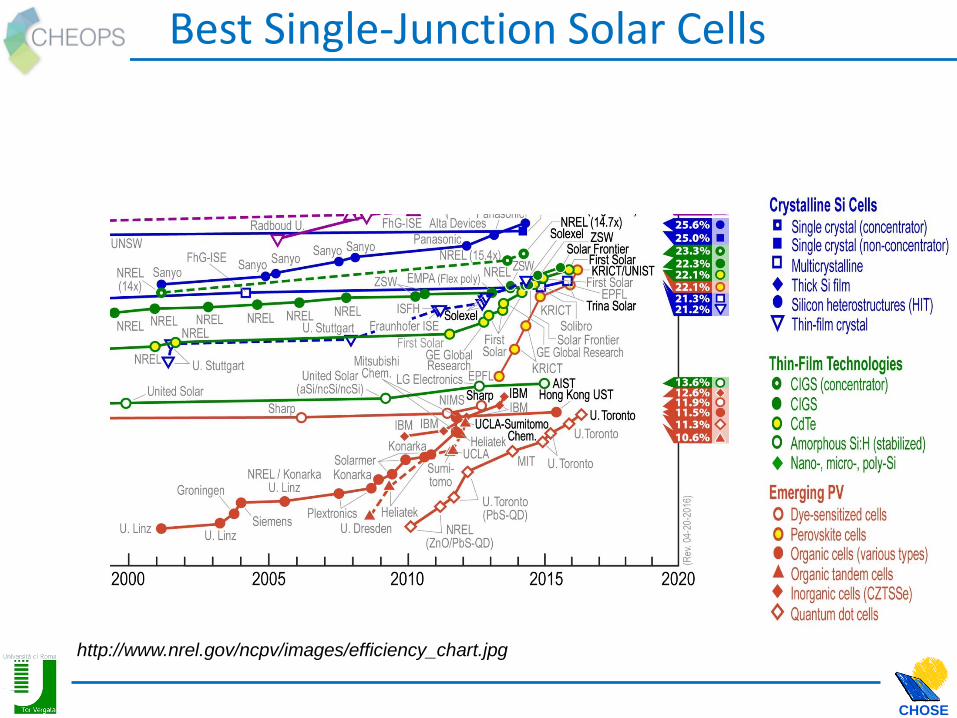
http://www.nrel.gov/ncpv/images/efficiency_chart.jpg
Best Single-Junction Solar Cells

CHOSE
Perovskite: ABX3 structure
Phase Transition (CH3NH3PbI3): Orthorhombic Tetragonal Cubic 162 K 327 K (54 C) The organic ligand is disordered in Tetragonal and Cubic phase.
Nature. 2013, 12, 1087 J. Mater. Chem. A, 2013, 1, 15628
Applications • Superconductivity • Fuel cells • Piezoelectric • Sensors • Solar cells • LEDs • Lasers

CHOSE
Panchromatic absorption & high absorption coefficient
Flexibility, transparency, low light workability
ambipolar charge-carrier
mobilities
long exciton lifetimes/diffusion
length
very low exciton binding energy
Up to 90% Absorption in Visible spectrum
Up to ~1 micron
How good are perovskite solar cells?
IPCE Fig Courtesy: H. S. Jung and N-G. Park, small, 2014
MAX3 can works as electron as well as hole transporter
Eperon, G. E., et al. (2014). ACS
Nano.
Hodes, G. (2013). Science 342, 317-318.

CHOSE
Tunable Band Gap
CH3NH3PbI3-xBrx Perovskite
By the insertion of Br atoms (x) on the
perovskite cristalline structure, the energy
gap can be increased.
Noh, J. H., S. H. Im, et al. (2013). Nano Lett 13(4): 1764-1769.

CHOSE
Monolithic Tandem PSC/c-Si
Conversion efficiency up to 20% on 1.5cm2

CHOSE
PSC Device Architecture
ABX3 Perovskite
p i
n
Heo, J. H., S. H. Im, et al. (2013 Nature Photonics 7(6): 486-491.
Light
TiO2/CH3NH3PbI3 /HTM
Good hole and electron diffusion length (from
100 nm to 1 μm)

CHOSE
Device: Mesostructured vs Planar B
oix
, P. P
., K. N
on
om
ura
, et a
l. (20
14
). "Cu
rren
t pro
gre
ss a
nd
futu
re p
ers
pe
ctiv
es fo
r
org
an
ic/in
org
anic
pe
rovskite
so
lar c
ells
." Ma
teria
ls T
od
ay 1
7(1
): 16-2
3.
Easier perovskite grown
Better charge collection
Easier perovskite grown
Better charge transport
Less production step
No sintering step
CHOSE
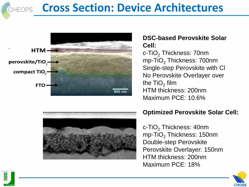
Cross Section: Device Architectures
DSC-based Perovskite Solar
Cell:
c-TiO2 Thickness: 70nm
mp-TiO2 Thickness: 700nm
Single-step Perovskite with Cl
No Perovskite Overlayer over
the TiO2 film
HTM thickness: 200nm
Maximum PCE: 10.6%
c-TiO2 Thickness: 40nm
mp-TiO2 Thickness: 150nm
Double-step Perovskite
Perovskite Overlayer: 150nm
HTM thickness: 200nm
Maximum PCE: 18%
Optimized Perovskite Solar Cell:
CHOSE
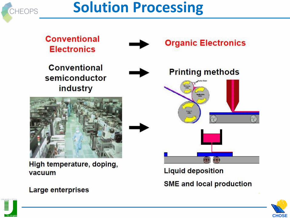
Solution Processing
CHOSE
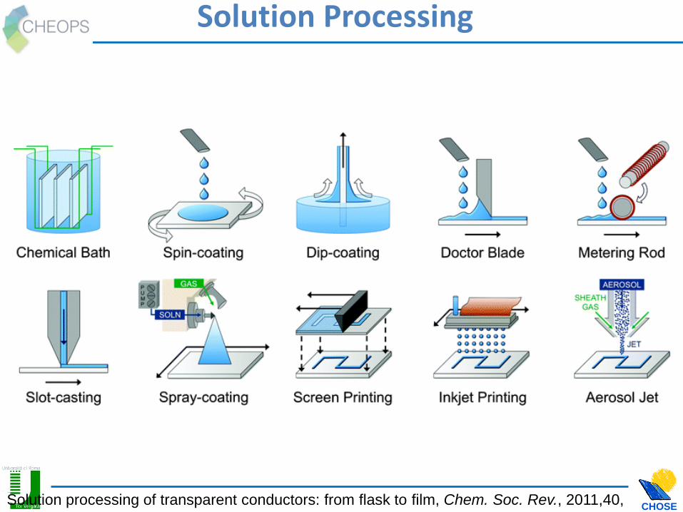
Solution Processing
Solution processing of transparent conductors: from flask to film, Chem. Soc. Rev., 2011,40,
5406-5441

CHOSE
Several deposition methods
Spin coating perovskite Drying RT Annealing 90-130°C
1) One-step procedure
1a) 3 CH3NH3I + PbCl2 → CH3NH3PbI3-xClx + …
CH3NH3I + Pbl2 → CH3NH3PbI3 1b) Solvent engineering
Nam Joong Jeon et al. Nature 517,476 (2015)
PbI2 deposition CH3NH3I dipping
Perovskite layer
2) Two-step procedure
J. Burschka, et al. Nature, 2013, 499, 316
CHOSE
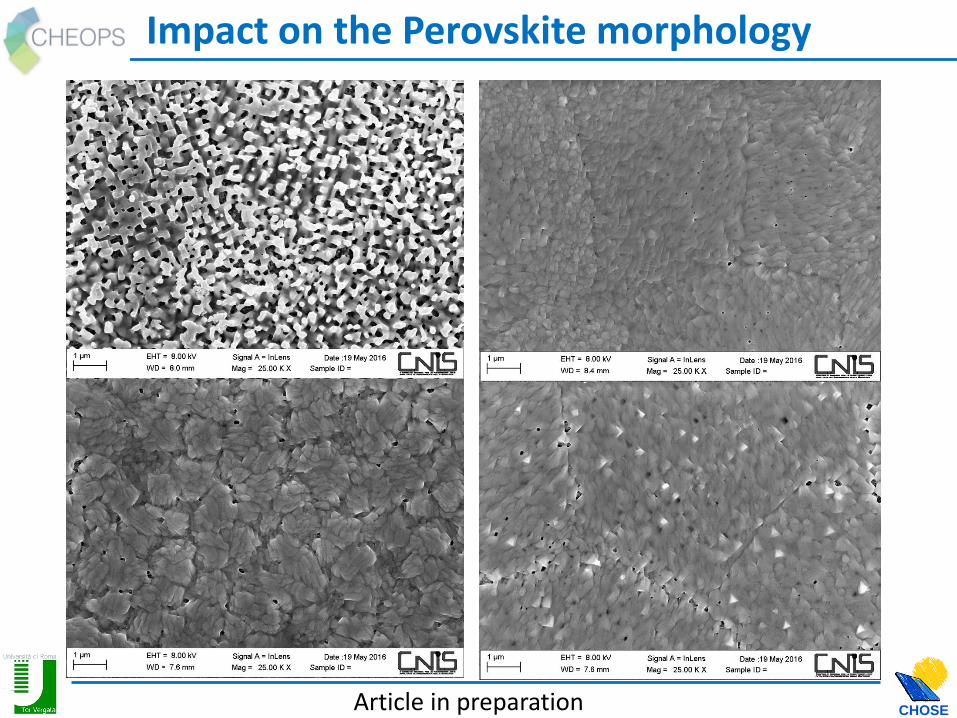
Impact on the Perovskite morphology
Article in preparation

CHOSE
Up-Scaling Process
10cm2
Up-scaling Issues:
Deposition Uniformity
Patterning Procedures
These issues have been studied to reduce:
• The PCE loss from small area to larger one
• The PCE loss from large area cells to the
module 100cm2
0.1cm2

CHOSE
Module Fabrication
FTO Patterning Screenprinted Mask c-TiO2 Deposition
Mask Removal n-TiO2 Deposition Perovskite Deposition
P3HT Deposition Gold Evaporation Module

CHOSE
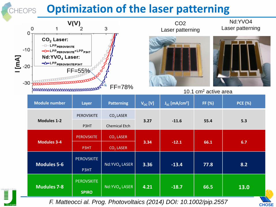
Laser Patterning Procedures (LPP)
CO2 Laser
(l=10µm) Au deposition
Nd:YVO4 Laser
(l=532nm)
Au deposition
LPPPEROVSKITE
nc-TiO2
FTO
BL-TiO2
Perovskite
LPPP3HT
CO2
Laser P3HT
LPPPEROVSKITE/P3HT
nc-TiO2
FTO
BL-TiO2
Perovskite
P3HT
F. Matteocci et al. Prog. Photovoltaics (2014) DOI: 10.1002/pip.2557
CHOSE
Optimization of the laser patterning
FF=78%
FF=55%
Module number Layer Patterning VOC [V] JSC [mA/cm2] FF (%) PCE (%)
Modules 1-2 PEROVSKITE CO2 LASER
3.27 -11.6 55.4 5.3 P3HT Chemical Etch
Modules 3-4 PEROVSKITE CO2 LASER
3.34 -12.1 66.1 6.7 P3HT CO2 LASER
Modules 5-6 PEROVSKITE
P3HT Nd:YVO4 LASER 3.36 -13.4 77.8 8.2
Mudules 7-8 PEROVSKITE
SPIRO Nd:YVO4 LASER 4.21 -18.7 66.5 13.0
CO2
Laser patterning
10.1 cm2 active area
F. Matteocci al. Prog. Photovoltaics (2014) DOI: 10.1002/pip.2557
Nd:YVO4
Laser patterning

CHOSE
Scaling-up issues: losses in FF and ISC
Scaling-up: perovskite solar modules
F. Matteocci, et al PCCP, 16 , 3918
PCE=5.1%
• Deposition Uniformity on the active
area
Active area = 10 cm2
Power= 130 mW
Spin coating
deposition F. Matteocci et al.- Prog. Phot. 24, 436 DOI: 10.1002/pip.2557
PCE=13.0%
Double step
deposition
16.8cm2
PCE=13%
Optimized
Laser
Patterning
• High series resistance
W. Qiu et al.-En. Env. Sci. 9, 484 DOI: 10.1039/C5EE03703D
PCE=14.9%
Single step
Active Area= 4 cm2
Power= 54 mW
Spin coating
deposition • Several recombinations paths .
CHOSE
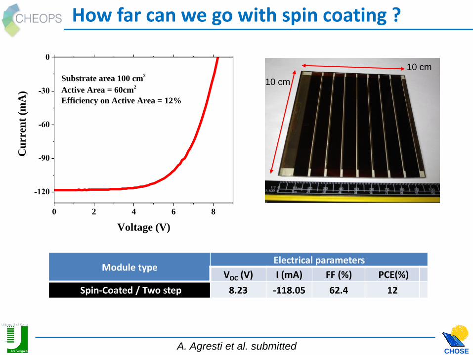
How far can we go with spin coating ?
Module type Electrical parameters
VOC (V) I (mA) FF (%) PCE(%)
Spin-Coated / Two step 8.23 -118.05 62.4 12
0 2 4 6 8
-120
-90
-60
-30
0
Cu
rren
t (m
A)
Voltage (V)
Substrate area 100 cm2
Active Area = 60cm2
Efficiency on Active Area = 12%
10 cm
10 cm
A. Agresti et al. submitted
CHOSE
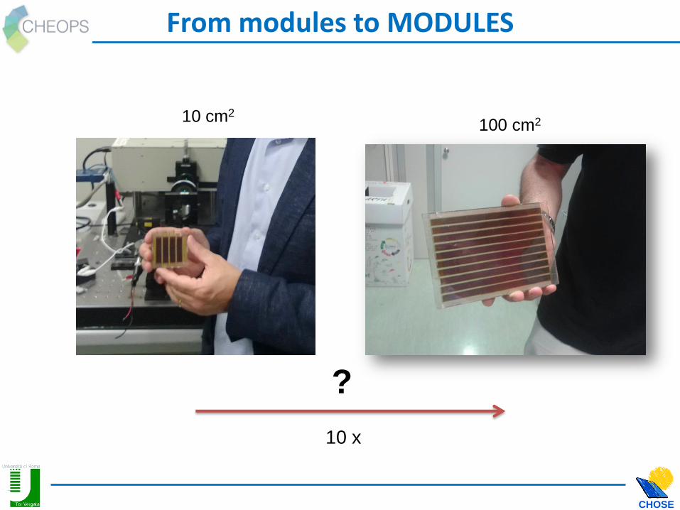
From modules to MODULES
10 x
10 cm2
100 cm2
?
CHOSE
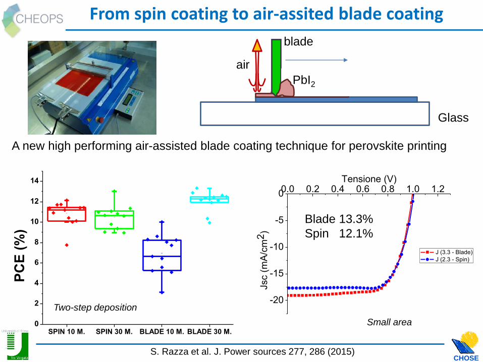
From spin coating to air-assited blade coating
SPIN 10 M. SPIN 30 M. BLADE 10 M. BLADE 30 M.0.0
0.2
0.4
0.6
0.8
1.0
1.2
Vo
c (
mV
)
SPIN 10 M. SPIN 30 M. BLADE 10 M. BLADE 30 M.0
5
10
15
20
Js
c (
mA
/cm
2)
SPIN 10 M. SPIN 30 M. BLADE 10 M. BLADE 30 M.0
2
4
6
8
10
12
14
PC
E (
%)
SPIN 10 M. SPIN 30 M. BLADE 10 M. BLADE 30 M.0
20
40
60
80
FF
(%
)
0.0 0.2 0.4 0.6 0.8 1.0 1.2
-20
-15
-10
-5
0
Jsc (
mA
/cm
2)
Tensione (V)
J (3.3 - Blade)
J (2.3 - Spin)
Blade 13.3%
Spin 12.1%
A new high performing air-assisted blade coating technique for perovskite printing
Two-step deposition
Small area
Glass
air
blade
PbI2
S. Razza et al. J. Power sources 277, 286 (2015)

CHOSE
Active area:100 cm2
PCE= 6.2 %
Power= 610 mW
Low quantity of solution required:
• Reduction of exposure to toxic agents
• Cost saving
Deposition over large area substrate:
• Control of deposition temperature
• Uniform deposition of active layer
Blade Coating deposition for large area
S. Razza et al. submitted
CHOSE
23
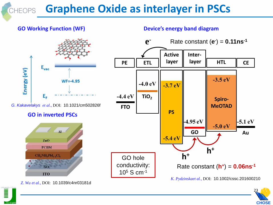
Device’s energy band diagram
GO in inverted PSCs
Z. Wu et al., DOI: 10.1039/c4nr03181d
G. Kakavelakys et al., DOI: 10.1021/cm502826f
GO Working Function (WF)
Rate constant (e-) = 0.11ns-1 e-
Rate constant (h+) = 0.06ns-1
GO hole
conductivity:
105 S cm-1 K. Pydzinskaet al., DOI: 10.1002/cssc.201600210
Graphene Oxide as interlayer in PSCs
CHOSE
Incident Photon to current
Conversion Efficiency (IPCE)
Absorbance
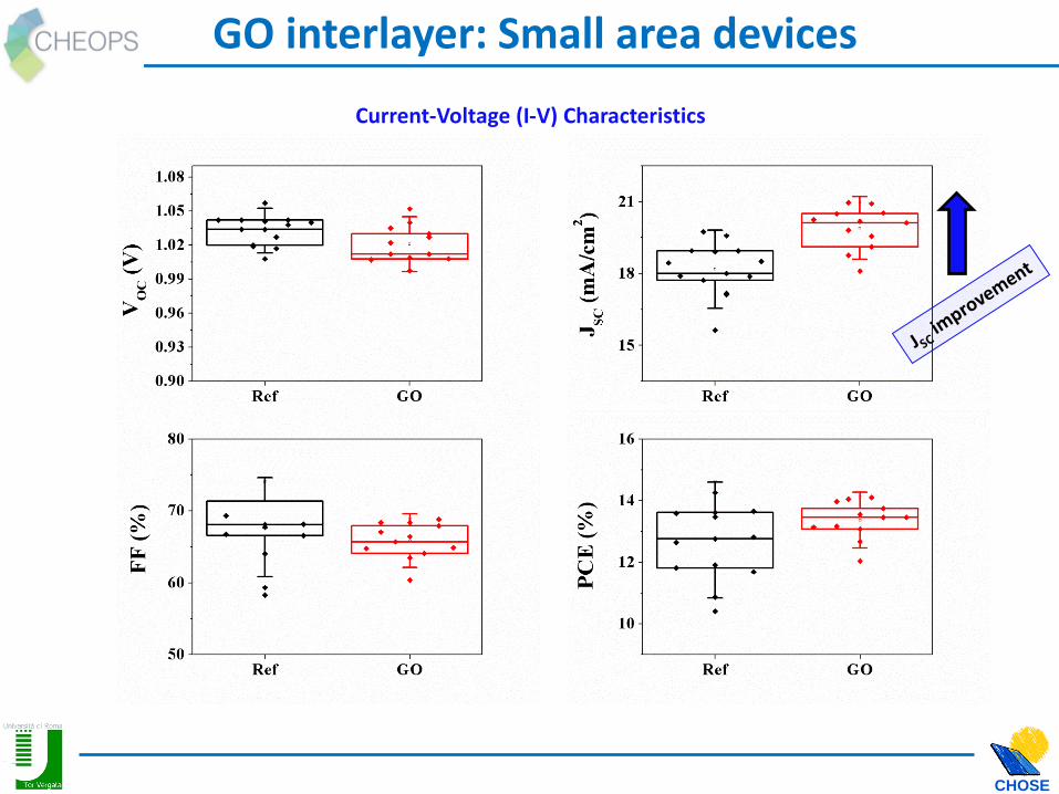
Current-Voltage (I-V) Characteristics
GO interlayer: Small area devices

CHOSE
Shelf life
IPCE
VOC rise profile
Dark I-V
Improved charge injection
Improved Perovskite/Spiro interface Improved charge injection and/or collection
Improved long-term stability
GO interlayer: Small area - Transient

CHOSE
Perovskite/GO/Spiro-MeOTAD - module showed improved PCE with an overall Pmax= 885 mW - Improved stability
VOC ISC FF PCE Pmax
Ref 8.96 114.2 59.9 6.21 612.8
GO 9.40 142.9 65.8 9.03 883.8
Graphene based module
PCE
S. Razza et al. submitted

CHOSE
Spray coated PEDOT back electrode
Module Jsc [ma/cm2]
Voc [V]
FF [%]
PCE [%]
PEDOT 9.56 7.99 41 3.47
PEDOT/Au 9.57 7.25 60 4.67
Full bladed module with PEDOT as back electrode
S. Razza et al. submitted

CHOSE
P1: Nd:YVO4, λ=1064 nm, 15 ns pulsed laser on FTO 44 μm wide scribing 200 μm wide spacing area P2: Nd:YVO4, λ=532 nm, 15 ns pulsed laser on SnO2/perovskite/HTM 700 μm wide etching 200 μm wide spacing area1 P3: Nd:YVO4, λ=532 nm, 15 ns pulsed laser 50 µm wide scribing
P1-P2-P3 on c-SnO2 Perovskite Solar Modules
P1-P2-P3 helps to increase the conversion efficiency on the aperture area (active area + interconnection area)

CHOSE
Sol-gel deposited c-SnO2 not efficient as c-TiO2
but easily permits P1-P2-P3 16,4 cm2 Active Area 18,95 cm2 Aperture Area 86,5% Aperture ratio PCE = 7.3% Aperture PCE = 6.31 %
P1-P2-P3 on c-SnO2 Perovskite Solar Modules
CHOSE
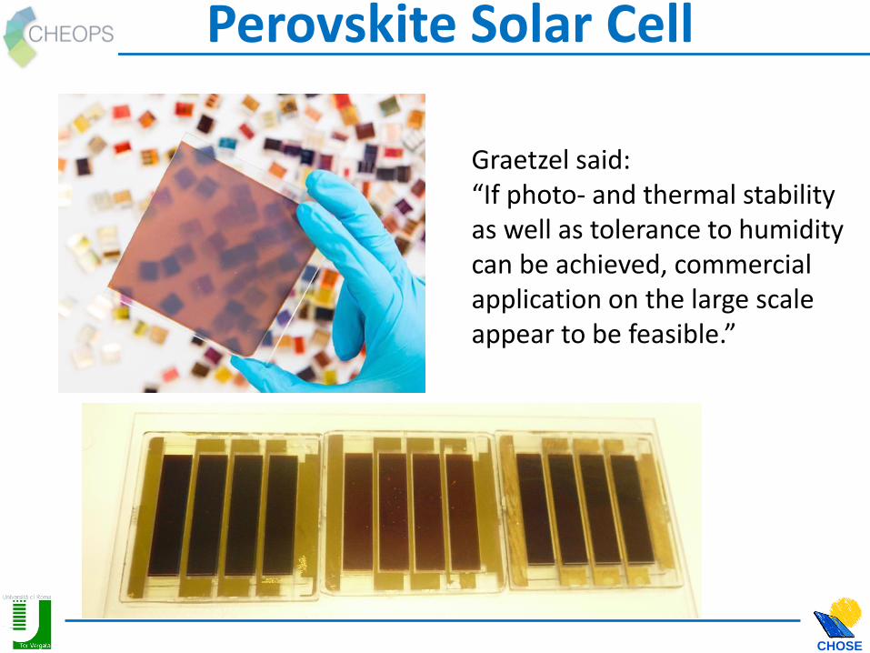
Perovskite Solar Cell
Graetzel said: “If photo- and thermal stability as well as tolerance to humidity can be achieved, commercial application on the large scale appear to be feasible.”

CHOSE
Stability issues
Thermal Stability
Environment Stability Light Stability
Issue: Moisture Effect Solutions: • Perovskite Composition • Sealing Procedure
Issues: Burn-in effect UV Degradation HTM Photo-oxidation Solutions: • UV Filter • Light Soaking up to
1Sun
Issues: Electrode Migration HTM dopants Solutions: • Morphology Control • Sealing • Polarization at MPP point
These degradation factors are present at the same time under real working conditions of the device. Moreover, in order to minimize the impact on the photovotaic parameters of each issue, it is crucial to separate each effects.

CHOSE
Intrinsic Stability
• Moisture
• Temperature
• Light Exposure
• Shading
• Polarization
Perovskite Degradation: Optical and Electrical Properties Interface: Perovskite/HTM Sealing: H2O Barrier HTM Stability: Pristine and Doped with Additives
80°C in air
CHOSE
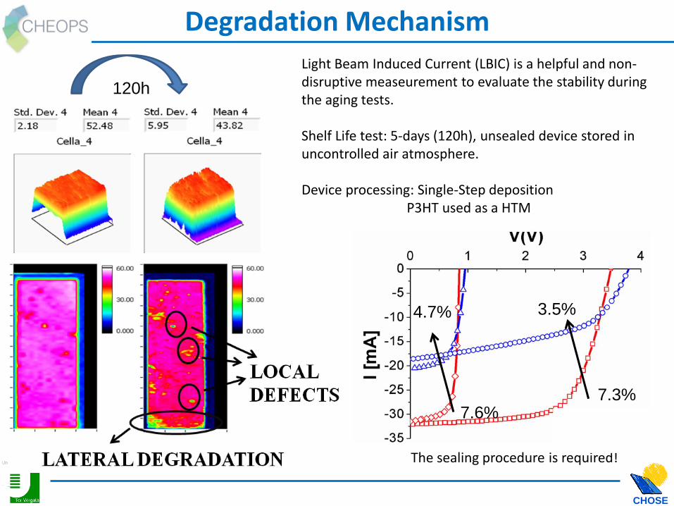
Degradation Mechanism
The sealing procedure is required!
7.6%
4.7%
7.3%
3.5%
Light Beam Induced Current (LBIC) is a helpful and non-disruptive measeurement to evaluate the stability during the aging tests. Shelf Life test: 5-days (120h), unsealed device stored in uncontrolled air atmosphere. Device processing: Single-Step deposition P3HT used as a HTM
120h

CHOSE
Sealing: Lateral Degradation
460h
730h 930h 1160h
260h 0h
Lateral Degradation due to the sealing failure appear since 260h .

CHOSE
Encapsulation Strategy & Stability
Article in press (Nano Energy)
• No effect of the sealing on the initial PV
performance
• Kapton adhesive film was laminated on the
device as primary sealing then a protective
glass was sealed to the device using a
methacrylate glue.
• An edge sealant was used to protect the
edge of the protective glass to limit the
moisture entrance.
SP-DES SP-D
Kapton
Adhesive
Light-curable
Glue
UV-curable
Glue as
edge
sealant
PSC
Device
Protective
Glass
F. Matteocci et al. NanoEnergy (2016) DOI: 10.1016/j.nanoen.2016.09.041

CHOSE
Investigation on Sealing Procedure
All Sealing Procedures are realized in air
The effect of sealing is mainly related to the curing processes

CHOSE
Stability: 1cm2 device
Main Issues: Deposition Uniformity (Jsc) TCO resistivity: (FF, Rs) HTL Properties (Voc) Architectures: Planar vs Meso Cost: Gold Replacement Safety: Lead content
Statistical investigation is needed
12 14 16 180
4
8
12
16
20
Coun
t
PCE (%)
0.1cm2
1.05cm2
Average PCE: Small Area (65samples) = 15% Large Area (23samples) = 13.6% Modules (3 samples) = 11.3%

CHOSE
Accelerated Life Time Tests
ISOS-D-1 Shelf: Mechanical Stability
ISOS-D-1-2 High Temp: Thermal Stability
ISOS-D-3 Damp: Humidity Test
ISOS-O-1: Light Stability
F. Matteocci et al. NanoEnergy (2016) DOI: 10.1016/j.nanoen.2016.09.041

CHOSE
Humidity Test
13.2% as initial PCE value RH = 95% T= 40-50°C
0.0 0.2 0.4 0.6 0.8 1.0
-20
-16
-12
-8
-4
0
Cu
rren
t [m
A/c
m2]
Voltage [V]
0h_PCE=13.3%
6h_PCE=12.1%
32h_PCE=10.6%
104h_PCE=10.4%Remarkable Voc decrease
F. Matteocci et al. Nano Energy (2016) DOI: 10.1016/j.nanoen.2016.09.041

CHOSE
Thermal Stability: STEM-HAADF technique
In order to overcome the stability issues, it is vital to understand the degradation pathways of
the structures involved, which here are observed for the first time at nanometer-scale spatial
resolution in situ, inside a scanning transmission electron microscope (STEM), while the
composition is monitored with elemental mapping through energy-dispersive X-ray analysis
(EDX).
FIB Lamella TEM analysis EDX maps
doi:10.1038/nenergy.2015.12
Nature Energy Article number: 15012 (2016)
CHOSE
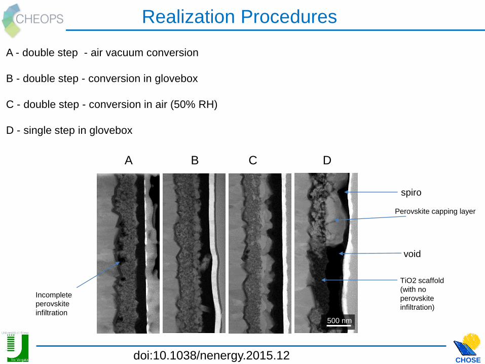
A - double step - air vacuum conversion
B - double step - conversion in glovebox
C - double step - conversion in air (50% RH)
D - single step in glovebox
A B C D
500 nm
void
spiro
Perovskite capping layer
TiO2 scaffold
(with no
perovskite
infiltration)
Incomplete
perovskite
infiltration
Realization Procedures
doi:10.1038/nenergy.2015.12

CHOSE
In-situ Heating
50°C 150°
C
200°
C
250°
C No change
in perovskite
layer until
150°C.
Leakage of iodine at the interface with perovskite and HTM
doi:10.1038/nenergy.2015.12
CHOSE
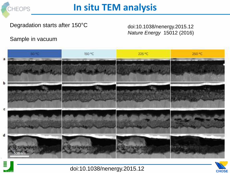
In situ TEM analysis
Degradation starts after 150°C
Sample in vacuum
doi:10.1038/nenergy.2015.12
Nature Energy 15012 (2016)
doi:10.1038/nenergy.2015.12
CHOSE
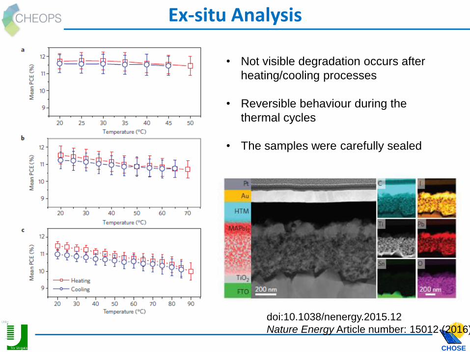
Ex-situ Analysis
• Not visible degradation occurs after
heating/cooling processes
• Reversible behaviour during the
thermal cycles
• The samples were carefully sealed
doi:10.1038/nenergy.2015.12
Nature Energy Article number: 15012 (2016)
CHOSE
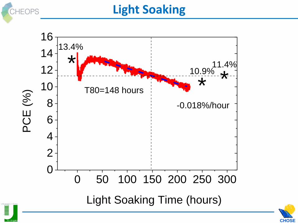
Light Soaking
0 50 100 150 200 250 3000
2
4
6
8
10
12
14
16
10.9%
*
P
CE
(%
)
Light Soaking Time (hours)
-0.018%/hour
*13.4%
T80=148 hours*
11.4%
CHOSE
Stability on module 5.7x5.7cm2
-20
-15
-10
-5
0
0 1 2 3 4
Voltage (V)
Curr
ent density (
mA
/cm
2)
0.0 0.5 1.0 1.5 2.0 2.5 3.0
0
2
4
6
8
10
12
14
PC
Em
pp (
%)
Time (min)
11.2% Stabilized PCE
13% Reverse 11.2% Stabilized
Sealed
@White LED (350mA)
After Laser Ablation
Bladed Spiro
>350 hours
Burn-in effect
After Gold Evaporation
Task 1.2.2 D.11
Good
Uniformity
N. Yaghoobi Nia et al in preparation

CHOSE
Lead content: Recycling Pb from Car Batteries
Lead content can be recycled from
exaust car batteries!

CHOSE
Conclusion
• The Perovskite-based photovoltaic technology could be competitive with respect to CdTe and CIGS thin films in terms of cost and performance.
• Suitable for optoelectronic applications: LED, Laser, Solar cells • Our up-scaling process demonstrates the feasibility of the solution processed
PSC on large area substrates.
• The use of 2d-materials play a role at the interface of the p-i-n architecture.
• Encapsulation is mandatory to evaluate only the intrinsic dgradation factors
• Stability: Promising results but we have to solve some issues regarding the detrimental effect of the light exposure on the costituent materials and interfaces.
CHOSE
Acknowledgments
MIUR
PRIN
DSSCX
AquaSol
Funds CHEETAH
DESTINY
GO-NEXTS
GRAPHENE-FLAGSHIP
FP7 CHEOPS
MOSTOPHOS
GRAPHENE-FLAGSHIP
H2020
Thank you for your
attention!