oxidative and initiated chemical vapor deposition of
TRANSCRIPT

i
Oxidative and Initiated Chemical Vapor Deposition of Polymer Electronic Materials
for Applications in Energy Conversion and Storage
A Thesis
Submitted to the Faculty
of
Drexel University
By
Siamak Nejati
In Partial Fulfilment of the
Requirements for the
Degree
Of
Doctor of Philosophy
April 2013

ii
© Copyright 2013
Siamak Nejati. All Rights Reserved.

iii
DEDICATION
To Mona for her true love and inspiration

iv
ACKNOWLEDGEMENTS
My first and foremost acknowledgement should and must go to my advisor, Dr. Kenneth Lau, a
patient man who walked me through my path in the past few years. His endless source of support
and wisdom inculcated in me a thirst for exploring innovative ideas. I was so lucky to work with
him and he will be a memorable figure in my life. I owe any measure of success I have so far
achieved to him. His kindness was above all. Not only I learned the path to be a good scientist
from him but also he taught me how to educate and teach. I am also grateful for the support and
guidance of my thesis committee, Dr. Jason Baxter, professor Masoud Soroush, Dr. Caroline
Schauer and Dr. Jonathan Spanier, who have all made measurable impacts on my development
during my time at Drexel. I also wish to express my sincere gratitude to professor Palmese, who
has generously offered help whenever I asked for and supported me financially and emotionally
when I find myself struggling with illness.
I would like to thank my other colleague at Drexel University who shared their knowledge with
me as well as hands-on training in lab. My past and present group mates, Dr. Ranjita Bose,
Stefani Susilo, Zakiya Carter, Arpit Patel, Danielle Martine, Laura Wu, Jahnavi Deshmukh,
Thomas Minford, Gregoty Wallowitch, Devin Cody, Sajeewa Ranasinghe, Noah Watson, Yuriy
Smolin and Chia-Yun Hsieh. I was also lucky enough to know many people from other
departments and groups. I would like to thank, Professor Anthony Addison, Dr. Volker Presser,
Dr. Edward Basgall, Timothy Wade, Dr. Stephen Dicker, Jared Cole and Elizabeth Plowman for
helping me in the lab with hands-on training. I am heartily grateful to many former and current
graduate students at Drexel University for their continuous help and support: Dr. Harsh Sharma,

v
Dr. Ali Emileh, Dr. Micheal Walter, Dr. Yuesheng Ye, Arianna Waters, James Throckmorton,
Taha Mohseni, Glenn Guglietta, Majid Sharifi, Min Heon, Eric Laird and Steven Spurgeon. To
all of my friends and colleagues your kindness will never be forgotten.
I would like to acknowledge the past and present staff at Chemical and Biological Engineering
department for their continuous help and support during my time at Drexel. Dan Luu, Dorothy
Gould, Jennifer Bing, Katie Brumbelow and Tracy McClure , thank you for all your help and
guidance. I am also grateful to the help and support provided by the Centralized Research Facility
at Drexel University and its core staff, Ms. Sahar Javedani and Craig Johnosn.
Finally, my path has led me thus far only with the support of my caring parents Mostafa Nejati,
Behrouz Bavarian, Roohangiz Beigi and Fatemeh Baradaran, my brothers Babak Nejati, Sina
Nejati and Mohamad Bavarian, my sisters Solmaz Alipour, Maryam Bavarian and Sara Bavarian
and my wife, Mona Bavarian. Mona was not only a great source of encouragement for me but
also she was a wise, knowledgeable colleague and collaborator who contributed to the solar cell
project with her sophisticated and smart approach in mathematical modelling of the system. It is
with you that I want to share this achievement.

vi
Table of Contents
List of Tables ................................................................................................................................... x
List of Figures ................................................................................................................................ xi
Abstract ...................................................................................................................................... xvii
1 Chapter 1: Introduction and Background ........................................................................... 1
1.1 Polymer synthesis using chemical vapor deposition ...................................................... 1
1.2 Initiated chemical vapor deposition ............................................................................... 2
1.3 iCVD polymer electrolytes for solar cell application..................................................... 4
1.4 Oxidative chemical vapor deposition ............................................................................. 5
1.5 Redox polymers for supercapacitor application ............................................................. 7
1.6 References ...................................................................................................................... 8
2 Chapter 2: Overall Objective and Specific Aims .............................................................. 15
Specific Aim 1: Synthesis of polymer electronic materials ...................................................... 15
Specific Aim 2: Integration of polymer electrolytes in dye sensitized solar cells .................... 15
Specific Aim 3: Integration of conducting polymers in supercapacitors .................................. 16
3 Chapter 3: Synthesis of Polymer Electronic Materials .................................................... 17
3.1 Introduction .................................................................................................................. 17
3.2 Poly(2-hydroxyethylmethacrylate) as a polymer electrolyte ....................................... 17
3.3 Experimental ................................................................................................................ 18
3.3.1 Polymer synthesis ................................................................................................. 18
3.3.2 Polymer characterization ...................................................................................... 18
3.4 Results and discussion ................................................................................................. 19
3.4.1 Fourier transform infrared spectroscopy .............................................................. 19

vii
3.4.2 X-ray photoelectron spectroscopy ........................................................................ 20
3.4.3 Gel permeation chromatography .......................................................................... 22
3.4.4 Electrochemical impedance spectroscopy ............................................................ 23
3.5 Unsubstituted polythiophene as a redox-active polymer ............................................. 25
3.6 Experimental ................................................................................................................ 27
3.6.1 Polymer deposition ............................................................................................... 27
3.6.2 Characterization ................................................................................................... 28
3.7 Results and discussion ................................................................................................. 29
3.7.1 Vibrational spectroscopy ...................................................................................... 30
3.7.2 X-ray photoelectron spectroscopy ........................................................................ 38
3.7.3 UV-vis spectroscopy ............................................................................................ 43
3.7.4 Cyclic voltammetry .............................................................................................. 45
3.7.5 Effect of oCVD processing conditions on polymer properties............................. 47
3.8 Conclusions .................................................................................................................. 51
3.9 References .................................................................................................................... 52
4 Chapter 4: Integration of Polymer Electrolytes in Dye Sensitized Solar Cells .............. 56
4.1 Introduction .................................................................................................................. 56
4.1.1 DSSC working principle ...................................................................................... 57
4.1.2 Replacing the liquid electrolyte ............................................................................ 59
4.1.3 Pore filling methodology ...................................................................................... 59
4.2 Experimental ................................................................................................................ 61
4.2.1 Electrode preparation ........................................................................................... 61
4.2.2 Pore filling ............................................................................................................ 61
4.2.3 Pore filing estimation ........................................................................................... 62
4.2.4 Dye sensitized solar cell fabrication ..................................................................... 63

viii
4.2.5 Solar cell characterization .................................................................................... 63
4.3 Results and discussion ................................................................................................. 64
4.3.1 TiO2 electrode porosity and surface area ............................................................. 64
4.3.2 Effect of process parameters on pore filling ......................................................... 65
4.3.3 Understanding pore filling dynamics ................................................................... 68
4.3.4 Pore filling quality ................................................................................................ 72
4.3.5 Polymer integrated DSSC performance ............................................................... 74
4.3.6 Electrochemical impedance spectroscopy ............................................................ 81
4.4 Conclusions .................................................................................................................. 83
4.5 References .................................................................................................................... 83
5 Integration of conducting polymers in supercapacitors ................................................... 87
5.1 Introduction .................................................................................................................. 87
5.2 Supercapacitors ............................................................................................................ 88
5.3 Experimental ................................................................................................................ 89
5.3.1 Polymer synthesis ................................................................................................. 89
5.3.2 Polymer characterization ...................................................................................... 90
5.3.3 TiO2 electrode fabrication .................................................................................... 92
5.3.4 Activated carbon electrode fabrication ................................................................. 92
5.3.5 Current collectors ................................................................................................. 93
5.3.6 oCVD polythiophene integration ......................................................................... 93
5.3.7 Polymer weight measurement .............................................................................. 94
5.4 Results and discussion ................................................................................................. 94
5.4.1 Vibrational spectroscopy ...................................................................................... 95
5.4.2 UV-vis spectroscopy ............................................................................................ 98
5.4.3 Cyclic voltammetry of the deposited film on FTO .............................................. 99

ix
5.4.4 Polymer integration within nanostructures ........................................................... 99
5.4.5 Effect of nanostructure on charge storage .......................................................... 102
5.4.6 Polymer integrated supercapacitors .................................................................... 108
5.5 Conclusions ................................................................................................................ 111
5.6 References .................................................................................................................. 111
6 Chapter 6: Conclusions and Future Directions .............................................................. 115
6.1 Specific aim 1............................................................................................................. 115
6.2 Specific aim 2............................................................................................................. 116
6.3 Specific aim 3............................................................................................................. 117
6.4 List of publications..................................................................................................... 118

x
List of Tables
Table 3.1. XPS elemental analysis of oCVD polythiophene and standard oligothiophenes. ....... 41
Table 3.2. Effect of oCVD synthesis conditions on polythiophene properties.Sample run.......... 49

xi
List of Figures
Figure 1.1. Reaction scheme and mechanism proposed for iCVD polymerization. ..................................... 3
Figure 1.2. iCVD reactor chamber. .............................................................................................................. 3
Figure 1.3. oCVD reactor showing the oxidant (blue) and monomer (red) vapor flows. ............................. 6
Figure 3.1. FTIR spectra of HEMA monomer, standard PHEMA and iCVD PHEMA. ............................ 20
Figure 3.2. XPS survey of 100 nm PHEMA deposited on Si (001) wafer. The C1s and O1s peak
intensities were used to evaluate the ratio of C:O. The peak around 1000 eV is the Auger peak of
oxygen. .......................................................................................................................................... 21
Figure 3.3. High resolution XPS signals of (a) oxygen 1s, and (b) carbon 1s............................................ 21
Figure 3.4. Refractive index detector intensity as a function of elution time in gel permeation
chromatography for (a) PEO calibration standards, and (b) iCVD PHEMA (A and B are deposited
using 0.2 and 0.4 sccm flow of initiator, respectively. .................................................................. 22
Figure 3.5. The Nyquist plot for a polymer electrolyte sandwiched between two Pt-coated FTO glass. The
data was fitted to a Randles equivalent circuit that included a Warburg impedance to derive the
conductivity and diffusion coefficient. .......................................................................................... 24
Figure 3.6. Conductivity of iCVD PHEMA incorporating different dielectric additives containing 0.05 M
I2 and 0.5 M LiI as a redox couple. ............................................................................................... 25
Figure 3.7. FTIR spectra of as-deposited and washed polythiophene. The doping induced vibrational
bands in the 1100-1500 cm-1
region for the as-deposited film disappear after washing as a result
of dedoping. ................................................................................................................................... 31
Figure 3.8. The (a) calculated and (b) experimental FTIR spectra of thiophene. ....................................... 33
Figure 3.9. The (a) calculated and (b) experimental FTIR spectra of bithiophene. .................................... 33
Figure 3.10. The (a) calculated and (b) experimental FTIR spectra of terthiophene. ................................ 34
Figure 3.11. The (a) calculated and (b) experimental FTIR spectra of quarterthiophene. ......................... 34

xii
Figure 3.12. Raman spectra of as-deposited and washed polythiophene. The spectra can be divided into
three main regions in the range of 1350-1500, 1000-1250 and 650-740 cm-1
. Insets magnify the
latter two regions of lower intensity. Washing results in narrowing of the peaks in the highest
intensity region as a result of a loss of the quinoid vibration. ....................................................... 36
Figure 3.13. Raman spectral fitting in the 1300-1500 cm-1
region of (a) as-deposited and (b) washed. .... 37
Figure 3.14. Raman spectral fitting in the (a) 1000-1250 and (b) 620-740 cm-1
regions of as-deposited
PTh. ............................................................................................................................................... 38
Figure 3.15. High resolution S2p XPS spectra of (a) washed and (b) as-deposited PTh. .......................... 39
Figure 3.16. High resolution Cl2p XPS spectra of (a) washed and (b) as-deposited PTh. ......................... 40
Figure 3.17. XPS survey spectra of washed polythiophene with C60 sputter depth profiling.
Compositional analysis yields a C:S ratio of 4.3:1, which is close to the theoretical value of 4:1. A
small amount of oxygen present (2.1 at%) is attributed to adsorbed oxygen species. Sputter depth
profiling using Ar+
shows the dopant has been effectively removed with the washing. The
maximum depth of acquisition is 10 nm and the spectra are separated equally by 2nm. .............. 41
Figure 3.18. High resolution (a) C1s and (b) S2p XPS spectra of washed polythiophene. Peak fits reveal
the expected 1:1 ratio of α andβcarbonsaswellasasinglesulfurspeciesofthethiophenering.
....................................................................................................................................................... 42
Figure 3.19. UV-vis spectra of as-deposited and washed polythiophene. The as-deposited film shows the
characteristic broad polaron absorption of the doped form while the dedoped film after washing
gives a single absorption peak at λmax = 470 nm of theπ-π*transition. ........................................ 44
Figure 3.20. UV-vis spectrum of the dissolved portion of PTh. ................................................................. 44
Figure 3.21. Correlation of λmax with the number of thiophene chain units, comparing literature data and
experimental data of undoped standard oligothiophenes with washed polythiophene and its
dissolved soluble fraction after washing. The correlation indicates a longer conjugation length

xiii
with a higher degree of polymerization. The correlation also indicates that the solid portion of the
washed film is much longer than 6-7 thiophene units while the dissolved fraction consists mainly
of 5 repeat units. ............................................................................................................................ 45
Figure 3.22. Cyclic voltammogram of washed polythiophene in a supporting electrolyte solution of
acetonitrile and tetraethylammonium hexafluorophosphate. The anodic and cathodic peaks are
observed at 1.1 and 0.6 V vs SCE, respectively. The corresponding film color in the oxidized and
reduced forms are also shown. ...................................................................................................... 46
Figure 3.23. Cyclic voltammetry sweep of PTh. ........................................................................................ 47
Figure 4.1. Dye sensitized solar cell layout. .............................................................................................. 57
Figure 4.2. Schematic of the pore filling process during initiated chemical vapor deposition (iCVD).
Monomer (M) and initiator (I) molecules are delivered into the reaction chamber in the form of
gaseous vapors. The initiator is selectively activated by a series of heated filaments. The activated
initiator (R) and monomer (M) adsorb onto the TiO2 surface within the nanostructured
mesoporous electrode that is kept cooled to enhance the adsorption-limited process. Addition
polymerization of the monomer at activated initiator sites results in the formation of a growing
polymer inside the pores. ............................................................................................................... 60
Figure 4.3. Nitrogen adsorption/desorption isotherm of the mesoporous electrode. .................................. 64
Figure 4.4. Effect of total pressure on pore filling, showing cross sectional SEM of the 4 µm thick TiO2
electrodes that are (a) uncoated, and after iCVD treatment at a total pressure of (b) 60, (c) 125,
and (d) 200 mtorr (scale bar=100 nm). Complete pore filling is observed at intermediate
pressures. ....................................................................................................................................... 66
Figure 4.5. The individual effect of the initiator and monomer on pore filling of TiO2 electrodes, showing
lack of complete pore filling at initiator flow rates of (a) 0.2, and (b) 0.3 sccm, and at monomer
flow rates of (c) 0.2, and (d) 0.6 sccm (scale bar=200 nm). Complete pore filling is observed at
initiator flow rates of 0.4 sccm and higher, and at a monomer flow rate of 0.4 sccm. .................. 67

xiv
Figure 4.6. Estimated time constants for monomer diffusion and reaction as a function of the monomer
relativepressure(solidlineisτD anddashedlineisτR)................................................................. 71
Figure 4.7. Pore filling of TiO2 electrodes of different thicknesses of (a) 4 µm (scale bar=500 nm), and (b)
12 µm (scale bar=1 µm), the inset shows the bottom of the sample (scale bar=500 nm). By
carefully controlling mass transport (gas and surface diffusion)................................................... 72
Figure 4.8. Thermogravimetricanalysisofthe12.6μmthickporefilledtitaniumdioxide.Cross-sectional
SEM showed 97±10 nm thick polymer overlayer. ........................................................................ 73
Figure 4.9. The filled mesoporous of thickness L with δ polymer overlayer. ............................................ 74
Figure 4.10. Current-voltage characteristics of DSSCs fabricated with the polymer electrolyte containing
50:50vol%propylenecarbonateandγ-butyrolactone(),andwiththestandard acetonitrile liquid
electrolyte()incorporatingrutheniumdyes(a)535orN3,and(b)505. .................................... 75
Figure 4.11. Effect of redox solvent on the performance of DSSCs fabricated with the polymer electrolyte
()andthecorresponding liquidelectrolyte()containing(a)50:50vol%propylenecarbonate
and γ-butyrolactone, and (b) pure propylene carbonate. In each case, Voc is enhanced while Jsc
remains relatively unchanged in the polymer electrolyte cell. ...................................................... 77
Figure 4.12. Current-voltage characteristics of DSSCs containing 50:50 vol% propylene carbonate and γ-
butyrolactonepore filled polymer electrolyte (), partially pore filled polymer electrolyte (),
andliquidelectrolyte(). .............................................................................................................. 77
Figure 4.13. Comparison between the performance of DSSCs fabricated with a quasi-solid state PHEMA
polymer electrolyte containing 50:50 vol% propylene carbonate and γ-butyrolactone(),andwith
astandardliquidelectrolytecontainingacetonitrile()fordifferentTiO2 thicknesses, showing (a)
open circuit voltage Voc, (b) short circuit current Jsc, (c) fill factor FF, and (d) power conversion
efficiency η (error bar=1 SD). Polymer electrolyte DSSCs provide similar efficiency as the liquid
electrolyte cells with TiO2 electrode thicknesses that are nearly three times thinner. ................... 79

xv
Figure 4.14. The effect of illuminated light intensity on short circuit current density of DSSCs utilizing
(a) liquid electrolyte, and (b) polymer electrolyte, each containing propylene carbonate with
different redox concentrations (in I2(M):LiI(M)) of 0.01:0.1 (∎), 0.08:0.8 (), and 0.2:2.0 ()
iodine and lithium iodide, respectively. ........................................................................................ 80
Figure 4.15. Comparison between the Bode diagrams at their respective Voc of DSSCs fabricated with the
polymer electrolyte () and the corresponding liquid electrolyte () containing propylene
carbonate. The shift of the mid-frequency peak to lower frequency of the polymer electrolyte cell
indicates a decrease in charge recombination at the electrolyte-electrode interface. .................... 82
Figure 5.1. FTIR spectrum of an as-deposited doped film on silicon. ....................................................... 95
Figure 5.2. Raman spectra of PTh deposited on silicon, excited using (a) 488, and (b) 633 nm laser beams.
....................................................................................................................................................... 97
Figure 5.3. Raman spectra of polythiophene deposited at different oCVD condition. The shift in quinod
peak to a lower wavenumber is concomitant with an increase in film electrical conductivity. .... 97
Figure 5.4. UV-vis spectrum of an as-deposited film after dedoping the film to its undoped form (by
exposure to 2.0 M methylamine in methanol for 2 min followed by washing with neat methanol).
Inset shows the control over absorption spectrum by changing oCVD parameters, the increase in
conjugation length obtained by reducing the oxidant concentration. ............................................ 98
Figure 5.5. Cyclic voltammogram of an as-deposited film on FTO glass. ................................................. 99
Figure 5.6. Conformal coating of polythiophene within porous nanostructures using oCVD. (a) Uncoated
anodized aluminum oxide (AAO) membrane, 57 µm thick and 200 nm pore diameter. (b)
Polythiophene coated AAO in the as-deposited doped state of the polymer. (c) Polythiophene
coated AAO in the undoped state of the polymer after dedoping. (d) Cross-sectional SEM of an
AAO membrane showing the porous channels (darker shade). (e) Cross-sectional SEM of a
polythiophene coated AAO membrane showing conformal and uniform. The conditions used for

xvi
filling AAO without mass transfer limitations up to 40 nm thick film on the inner wall was as
follow: 30 °C stage temperature, and 0.1, 2 and 2 sccm of initiator, monomer and N2, and 800
mtorr total pressure. ..................................................................................................................... 101
Figure 5.7. Polythiophene integrated TiO2 electrodes. (a) Undoped PTh (by exposure to 2.0 M
methylamine in methanol for 2 min followed by washing with neat methanol). (b) Cross-
sectional SEM of the mesoporous electrode with conformal PTh coating (scale bar is 200 nm).
..................................................................................................................................................... 102
Figure 5.8. Cyclic voltammograms at different scan rates of PTh deposited within mesoporous TiO2
electrodes recorded in a three electrode set up versus an Ag/AgCl reference electrode. ............ 103
Figure 5.9. Effect of polymer thickness and 3D nanostructure on the specific capacitance of oCVD
polythiophene. (a) SEM images (scale bar is 200 nm) and specific capacitance values of thin (250
nm) and thick (800 nm) films on planar FTO electrodes, and of thin (4 nm) and thick (6 nm) films
inside mesoporous electrodes of TiO2; specific capacitance is based on per mass of polymer and
reported with 2 standard deviations. The current density of the anodic peak (doping peak) as a
function of scan rate for different thickness of films on (b) planar substrates and (c) within
mesoporous nanostructures. ........................................................................................................ 107
Figure 5.10. Electrochemical behavior of oCVD polythiophene coated activated carbon. SEM images of
activated carbon electrodes (a) without coating, and coated with polythiophene at polymer-to-
activated carbon mass ratios of (b) 1:1, (c) 1.5:1, and (d) 2.7:1 (insets show a magnified region of
the surface morphology of each sample; scale bar is 1 µm and 50 nm for the inset). (e) Specific
capacitance values based on per total mass of electrode for different polymer mass loadings.
Measurements were made at 100 mV/s for five different samples at each loading with the error
bars representing two standard deviations. (f) Cyclic voltammograms of the 1.5:1 mass ratio
pesudocapacitor recorded at different scan rates between –2 and 2 V. (g) Capacitance of the same
sample measured up to 5000 cycles (at 100 mV/s ). ................................................................... 110

xvii
Abstract
Oxidative and Initiated Chemical Vapor Deposition of Polymer Electronic Materials
for Applications in Energy Conversion and Storage
Siamak Nejati
Kenneth K. S. Lau Supervisor, Ph.D.
Initiated and oxidative chemical vapor deposition (iCVD/oCVD) are novel surface
polymerization techniques for the formation of polymer thin films. Taking advantage of a vacuum
environment, polymer CVD enables the synthesis of stoichiometric polymers that can be applied
on different surface geometries down to nanometer scale. In iCVD and oCVD, the surface
adsorption of reactive species is typically the limiting step, which means the polymer growth and
properties can be tuned by adjusting the surface availability of the reactants. In this work, iCVD
and oCVD were utilized for the synthesis and integration of electronic polymer materials in the
nanostructured electrodes of energy conversion and storage devices. iCVD was used to synthesize
poly(2-hydroxyethyl methacrylate) (PHEMA) as a potential polymer electrolyte while oCVD was
used to make unsubstituted polythiophene (PTh) as a potential electrically conducting polymer.
PHEMA was then integrated within the mesoporous electrode of dye sensitized solar cells and
iCVD conditions that enabled successful pore filling were identified. The resulting devices
fabricated with iCVD PHEMA polymer electrolyte showed superior performance when compared
to their liquid counterparts. PTh was integrated in the porous electrode of activated carbon
supercapacitors and oCVD conditions that enabled conformal ultrathin coating were found. The
resulting devices with oCVD PTh was found to have significantly higher charge storage capacity
as a result of the synergistic effect of the redox polymer and the nanostructured topology. Overall,
this work demonstrated the viability of iCVD and oCVD pathways for the design, synthesis, and

xviii
processing of polymers in nanostructured architectures for energy applications. Success
ultimately depended on a clear understanding of the fundamental kinetic and transport
mechanisms for enabling polymer integration.

1
1 Chapter 1: Introduction and Background
1.1 Polymer synthesis using chemical vapor deposition
Polymers, the building blocks of many things around us, are usually synthesized through
different chemistries in a liquid media. Whether the polymer is synthesized through step or chain
polymerization, the processing of the polymer requires additional processing steps. Except for
in-situ polymerization which is not always an easy process to undertake in the liquid phase, to
use the resulting polymers as an active component of devices spray coating, spin coating and
solvent casting are among the most frequently used methods.1 All these methods utilize polymer
solutions which necessitates the use of solvents. In many cases solvent entrapment in the final
product or device that benefit from the polymeric material is detrimental to product performance.
Also for many applications integrating polymers within high aspect ratio geometries is needed.
In this case, using conventional liquid processing methods might be difficult due to surface
tension forces, lack of wettability, and solution viscosity that tend to lead to partial blockage of
the structure and non-conformal coating through the structure.
The ability to integrate polymers within confined geometries and nanoscale domains,2-5
such
as in the electrodes6 of solar cells and organic light emitting diodes (OLEDs), is expected to
enhance interfacial properties that could lead to improved device performance. Chemical vapor
deposition (CVD) is a viable approach for the synthesis and integration of polymers that
combines polymerization and coating in a single step at an interface. This way the polymer is
being directly applied to the substrate of interest. Using CVD the main challenges associated
with polymer integration can be addressed as the process is solvent free and the polymerization
is done in-situ and under vacuum conditions. There are two novel CVD processes that have
demonstrated suitability for polymer synthesis and coating which have been studied in this

2
thesis, namely initiated chemical vapour deposition (iCVD) and oxidative chemical vapour
deposition (oCVD).
1.2 Initiated chemical vapor deposition
In iCVD, as shown in Figure 1.1, a gaseous mixture of initiator and monomer vapors is
introduced into a vacuum chamber. The initiator is activated in the gas phase by a resistively
heated filament suspended 1-3 cm above a cooled substrate. The filament temperature is mild
enough that the monomer is not thermally degraded. The monomer and the activated initiator
(typically a primary free radical species) then adsorb onto the substrate. The monomer adds to
the activated initiator sites to initiate and propagate polymer chain radicals. Finally, these
polymer radical chains terminate leading to the formation of a polymer thin film.7 Figure 1.2
shows an iCVD reactor in our facility. iCVD is suitable technique for depositing polymer films
on heat sensitive substrates as the typical substrate temperature is around room temperature. In
typical iCVD synthesis conditions, the process is adsorption limited as evidenced by the faster
polymer growth rate with lower substrate temperatures. When using free radical initiation, the
mechanism of iCVD follows a radical polymerization scheme that has been confirmed by kinetic
modeling.8 In iCVD reactant vapors are metered through needle valves or mass flow controllers
via a heated delivery manifold upstream of the reactor. A vacuum pump downstream creates the
vacuum and a downstream throttle valve along with a Baratron capacitance pressure gauge are
used together with a pressure controller to maintain a desired pressure. To control resulting
polymer properties, iCVD parameters including the gas phase concentration of the reactants,
which can be adjusted by the total pressure and flow rate, as well as the substrate temperature,
which determines surface adsorption, are among the major iCVD parameters to consider

3
Figure 1.1. Reaction scheme and mechanism proposed for iCVD polymerization.8
Figure 1.2. iCVD reactor chamber.
By adjusting these iCVD parameters carefully, iCVD can produce exceptionally clean
polymers with stoichiometric composition and tunable molecular weight with no residual
solvents or impurities, and importantly iCVD polymers can be integrated into complex

4
topological geometries. Since the birth of iCVD, there has been tremendous development in the
polymers that can be synthesized through iCVD, including polytetrafluoroethylene,9-13
acrylates,7,8
methacrylates,14-19
and styrenes.20,21
iCVD has also shown to be a promising method
for producing copolymers22-29
and crosslinked polymers26,30-38
by utilizing more than one
monomer or a crosslinker. Due to the wide range of polymer chemistries and functionalities that
can be made use of, iCVD has been demonstrated in many different applications such as
biomedical implants,39-42
controlled chemical release,25,30,42,43
sensors,29,44-46
antimicrobial,47-48
low surface energy,49-52
dielectric coatings,53,54
and polymer electrolytes and polyelectrolytes.55-57
As mentioned earlier, in iCVD due to the absence of liquids conformal coating at the micro and
nanoscale can be achieved easily. Attempts to coat complex 3D structures using iCVD has
shown great promise30,42,43,58
and there seems to be a new wave of polymer applications relying
on the engineering of polymer coatings within nanostructures.59-63
1.3 iCVD polymer electrolytes for solar cell application
Polymer electrolytes are attractive from the point of practical applications as they have decent
ion conductivity, are low cost, have good stability, and are easy to process. Polymer electrolytes
can be used as a dry solid or they can be gelled by trapping an organic liquid such as ethylene
carbonate (EC), propylene carbonate (PC) or acetonitrile (AcN) into the polymer matrix to
improve ion conductivity. The application of polymer electrolytes in lithium batteries,64
electrochromic devices,65-67
and especially in dyes sensitized solar cells (DSSCs)68-70
have been
of great interest and numerous studies have been devoted to integrating these polymers within
active electrode materials.
Here, iCVD is used for depositing poly(2-hydroxyethyl methacrylate) (PHEMA) as a
potential polymer gel electrolyte for DSSCs to replace the current liquid electrolyte used in the

5
cell. Previous work with poly(methyl methacrylate) (PMMA) has shown improved performance
for gel electrolyte base devices.64,65,70
The importance of this study is to evaluate the potential of
iCVD in the synthesis and integration of PHEMA polymer electrolyte into DSSCs and to assess
the resulting device performance.
1.4 Oxidative chemical vapor deposition
In oCVD, as shown in Figure 1.3, a gaseous mixture of monomer and oxidant is introduced into
a vacuum chamber.71,72
Unlike iCVD, there is no need to thermally activate the oxidant initiator
molecule. If chosen properly, the oxidant will spontaneously enable the oxidative polymerization
of a redox active monomer such as thiophene or pyrrole. The proposed mechanism is believed to
be the formation of radical cations similar to a Friedel-Crafts chemistry using oxidants that show
Lewis acid character like FeCl3.72
The radical cation act as a propagation unit and can go through
step polymerization by attaching to another monomer unit and transferring the cation to the new
unit or by reacting with another radical cation.73,74
Oxidative chemistry has been widely
practiced through chemical and electrochemical pathways in the liquid phase for synthesizing
conductive polymers.75
The wealth of synthesis knowledge and the current growing interest in conductive polymers
for different applications such as solar cells,76,77
light emitting diodes,78-80
supercapacitors,81-83
antistatic surfaces,84
and electrochromic devices65,85
present a great opportunity for oCVD
particularly with its unique capability to form thin conformal wrinkle-free coatings. The initial
attempt with CVD polymerization of conjugated polymers date back to 1986 when Mohamadi
and co-workers exposed a cooled substrate which was covered by an oxidant (FeCl3) to a vapor
of monomers (thiophene and pyrrole).86-88
Later Winther-Jensen and other researchers adapted a

6
similar method named vapor phase polymerization (VPP) and synthesized exceptionally high
conductivity polymer.89,90
In comparison with VPP, oCVD is a continuous method which relies on the delivery of the
reactants (both oxidant and monomer) as vapors instead of relying on an oxidant-coated
substrate. In a similar fashion to iCVD, reactant vapors are metered through needle valves or
mass flow controllers via a heated delivery manifold upstream of the reactor again a vacuum
pump downstream creates the vacuum and downstream throttle valve along with a Baratron
capacitance pressure gauge are used together with a pressure controller to maintain a constant
desired pressure. To tune polymer properties again oCVD synthesis conditions, including the
surface and gas phase concentrations of the reactants can be adjusted by changing vapor flow
rates of the components and the substrate temperature. By adjusting oCVD parameters carefully,
conjugated polymer with desirable properties can be integrated into different geometries and
since oCVD is typically operated at low pressure again using proper condition high aspect ratio
structures can be filled or coated as desired.
Figure 1.3. oCVD reactor showing the oxidant (blue) and monomer (red) vapor flows.

7
1.5 Redox polymers for supercapacitor application
Conjugated polymers have been widely investigated as energy storage materials, due to their
large pseudocapacitance that emanate from their ability to be p or n doped. The fact that upon
doping the material becomes conductive means that they can store charge in their whole volume,
which when compared to a physical electrochemical double layer capacitance should result in
higher charge storage capacity.
In the past 20 years a great deal of attention has been devoted to the design and fabrication
of supercapacitors that makes use of conductive polymers. Among different classes of
conjugated polymers, polythiophenes due to their environmental stability have been the subject
of many studies. Polythiophene, poly(3,4-ethylenedioxythiophene), polypyrrole, polyaniline and
composites of these materials have been evaluated in supercapacitor devices,81-83, 91-98
and very
recently the importance of nanostructuring the electrodes incorporating these polymers have
resulted in enhanced charge storage and stability.94-97
oCVD have shown to be a very promising method in the synthesis and coating of conjugated
polymers with control over coating down to the nanoscale.99,100
Here oCVD is used to synthesis
polythiophene using a Lewis acid oxidant to enable oxidative polymerization. By adjusting
oCVD conditions, polythiophene can be integrated within porous activated carbon electrodes to
create pseudocapacitors. The importance of this study is to understand the role of the
nanostructure on charge storage in redox-active polythiophene.
The thesis therefore continues with the following: Chapter 2 describes the overall objective
and specific aims of this thesis. Chapters 3, 4 and 5 describe the work in each of the three
specific aims in detail. Chapter 3 discusses the iCVD synthesis of PHEMA and the oCVD
synthesis of unsubstituted polythiophene as potential polymer electronic materials. Chapter 4
discusses the integration of iCVD polymer electrolytes within the nanostructured electrodes dye

8
sensitized solar cells and the impact of the polymer on device behavior. Chapter 5 discusses the
integration of unsubstituted polythiophene within the nanostructured electrodes of
supercapacitors and the impact of the polymer on device behavior, Finally, Chapter 6 gives the
overall conclusions and describes the unique contributions of this thesis as well as offers some
possible future directions stemming from this work.
1.6 References
1. L. Ferrante, Handbook of Applied Polymer Processing Technology, CRC Press, Harpers
Ferry, USA 1996.
2. S.-J. Moon, Y. Itzhaik, J. H. Yum, S. M. Zakeeruddin, G. Hodes and M. Grätzel,
Journal of Physical Chemistry Letters, 2010, 1, 1524-1527.
3. G. K. Mor, S. Kim, M. Paulose, O. K. Varghese, K. Shankar, J. Basham and C. A.
Grimes, Nano Letters, 2009, 9, 4250-4257.
4. D. C. Olson, Y. J. Lee, M. S. White, N. Kopidakis, S. E. Shaheen, D. S. Ginley, J. A.
Voigt and J. W. P. Hsu, Journal of Physical Chemistry C, 2007, 111, 16640-16645.
5. K. Shankar, G. K. Mor, H. E. Prakasam, O. K. Varghese and C. A. Grimes, Langmuir,
2007, 23, 12445-12449.
6. J. S. Miller, Advanced Materials, 1993, 5, 671-676.
7. K. K. S. Lau and K. K. Gleason, Macromolecules, 2006, 39, 3688-3694.
8. K. K. S. Lau and K. K. Gleason, Macromolecules, 2006, 39, 3695-3703.
9. B. A. Cruden, K. K. Gleason and H. H. Sawin, Journal of Vacuum Science &
Technology B, 2002, 20, 690-695.
10. E. D. Laird, R. K. Bose, W. Wang, K. K. S. Lau and C. Y. Li, Macromolecular Rapid
Communications, 2013, 34, 251-256.
9
11. K. K. S. Lau, J. Bico, K. B. K. Teo, M. Chhowalla, G. A. J. Amaratunga, W. I. Milne,
G. H. McKinley and K. K. Gleason, Nano Letters, 2003, 3, 1701-1705.
12. S. Limb, K. S. Lau, D. Edell, E. Gleason and K. Gleason, Plasmas and Polymers, 1999,
4, 21-32.
13. H. G. Pryce Lewis, J. A. Caulfield and K. K. Gleason, Langmuir, 2001, 17, 7652-7655.
14. R. Bakker, V. Verlaan, C. H. M. van der Werf, J. K. Rath, K. K. Gleason and R. E. I.
Schropp, Surface and Coatings Technology, 2007, 201, 9422-9425.
15. K. K. S. Lau and K. K. Gleason, Advanced Materials, 2006, 18, 1972-1977.
16. M. Ma, Y. Mao, M. Gupta, K. K. Gleason and G. C. Rutledge, Macromolecules, 2005,
38, 9742-9748.
17. Y. Mao, N. M. Felix, P. T. Nguyen, C. K. Ober and K. K. Gleason, Journal of Vacuum
Science & Technology B, 2004, 22, 2473-2478.
18. Y. Mao and K. K. Gleason, Langmuir, 2004, 20, 2484-2488.
19. Y. Mao and K. K. Gleason, Macromolecules, 2006, 39, 3895-3900.
20. W. E. Tenhaeff and K. K. Gleason, Surface and Coatings Technology, 2007, 201, 9417-
9421.
21. W. Jo, K. Freedman, D. K. Yi, R. K. Bose, K. K. S. Lau, S. D. Solomon, M. J. Kim,
Biofabrication, 2011, 3, 015002.
22. A. K. H. Achyuta, A. J. White, L. H. G. Pryce and S. K. Murthy, Macromolecules, 2009,
42, 1970-1978.
23. S. G. Im, K. W. Bong, C.H. Lee, P. S. Doyle and K. K. Gleason, Lab on a Chip, 2009, 9,
411-416.
24. S. G. Im, B.-S. Kim, W. E. Tenhaeff, P. T. Hammond and K. K. Gleason, Thin Solid
Films, 2009, 517, 3606-3611.
25. S. J. P. McInnes, E. J. Szili, S. A. Al Bataineh, J. Xu, M. E. Alf, K. K. Gleason, R. D.
Short and N. H. Voelcker, ACS Applied Materials & Interfaces, 2012, 4, 3566-3574.

10
26. V. Raghunathan, J. L. Yague, J. Xu, J. Michel, K. K. Gleason and L. C. Kimerling,
Optics Express, 2012, 20, 20808-20813.
27. J. Xu and K. K. Gleason, Chemistry of Materials, 2010, 22, 1732-1738.
28. R. Yang and K. K. Gleason, Langmuir, 2012, 28, 12266-12274.
29. Y. Ye, Y. Mao, H. Wang and Z. Ren, Journal of Materials Chemistry, 2012, 22, 2449-
2455.
30. R. K. Bose, A. M. Heming and K. K. S. Lau, Macromolecular Rapid Communications,
2012, 33, 1375-1380.
31. R. K. Bose and K. K. S. Lau, Biomacromolecules, 2010, 11, 2116-2122.
32. K. Chan and K. K. Gleason, Langmuir, 2005, 21, 8930-8939.
33. K. Chan, L. E. Kostun, W. E. Tenhaeff and K. K. Gleason, Polymer, 2006, 47, 6941-
6947.
34. A. M. Coclite, G. Ozaydin-Ince, R. d'Agostino and K. K. Gleason, Macromolecules,
2009, 42, 8138-8145.
35. Lau, K. K. S.; Mao, Y.; Lewis, H. G. P.; Murthy, S. K.; Olsen, B. D.; Loo, L. S.;
Gleason, K. K., Thin Solid Films 2006, 501, (1-2), 211-215.
36. N. Mari-Buye, S. O'Shaughnessy, C. Colominas, C. E. Semino, K. K. Gleason and S.
Borros, Advanced Functional Materials, 2009, 19, 1276-1286.
37. I. G. Ozaydin, G. Demirel, K. K. Gleason and M. C. Demirel, Soft Matter, 2010, 6,
1635-1639.
38. G. Ozaydin-Ince and K. K. Gleason, Chemical Vapor Deposition, 2010, 16, 100-105.
39. A. K. H. Achyuta, V. S. Polikov, A. J. White, H. G. P. Lewis and S. K. Murthy,
Macromolecular Bioscience, 2010, 10, 872-880.
40. W. S. O'Shaughnessy, D. J. Edell and K. K. Gleason, Thin Solid Films, 2009, 517, 3612-
3614.

11
41. W. S. O'Shaughnessy, S. K. Murthy, D. J. Edell and K. K. Gleason, Biomacromolecules,
2007, 8, 2564-2570.
42. K. K. S. Lau and K. K. Gleason, Surface and Coatings Technology, 2007, 201, 9189-
9194.
43. K. K. S. Lau and K. K. Gleason, Macromolecular Bioscience, 2007, 7, 429-434.
44. L. Montero, G. Gabriel, A. Guimera, R. Villa, K. K. Gleason and S. Borros, Vacuum,
2012, 86, 2102-2104.
45. C. D. Petruczok, S. Y. Yang, A. Asatekin, K. K. Gleason and G. Barbastathis,
Microelectromechanical Systems, 2013, 22,54-61
46. W. E. Tenhaeff, L. D. McIntosh and K. K. Gleason, Advanced Functional Materials,
2010, 20, 1144-1151.
47. T. P. Martin, K. Chan and K. K. Gleason, Thin Solid Films, 2008, 516, 681-683.
48. T. P. Martin, S. E. Kooi, S. H. Chang, K. L. Sedransk and K. K. Gleason, Biomaterials,
2006, 28, 909-915.
49. M. Gupta and K. K. Gleason, Langmuir, 2006, 22, 10047-10052.
50. M. Ma, Y. Mao, M. Gupta, K. K. Gleason and G. C. Rutledge, Macromolecules, 2005,
38, 9742-9748.
51. Y. Mao and K. K. Gleason, Macromolecules, 2006, 39, 3895-3900.
52. C. T. Riche,B. C. Marin, N. Malmstadt and M. Gupta, Lab on a Chip, 2011,11, 3049-
3052
53. R. Bakker, P. Weijers, D. A. Spee, S. M. J. van, d. W. C. H. M. van, J. K. Rath and R. E.
I. Schropp, Thin Solid Films, 2011, 519, 4418-4420.
54. N. J. Trujillo, Q. Wu and K. K. Gleason, Advanced Functional Materials, 2010, 20, 607-
616.
55. R. K. Bose, S. Nejati and K. K. S. Lau, ECS Transanctions, 2009, 25, 1229-1235.
56. A. M. Coclite, P. Lund, R. Di Mundo and F. Palumbo, Polymer, 2013, 54, 24-30.

12
57. S. Nejati and K. K. S. Lau, Thin Solid Films, 2011, 519, 4551-4554.
58. K. K. Lau, J. Bico, K. B. Teo, M. Chhowalla, G. A. Amaratunga, W. I. Milne, G. H.
McKinley and K. K. Gleason, Nano Letters, 2003, 3, 1701-1705.
59. A. Asatekin and K. K. Gleason, Nano Letters, 2010, 11, 677-686.
60. A. Asatekin and K. K. Gleason, ACS Symposium Series, 2011, 1078, 39-50.
61. M. Gupta, V. Kapur, N. M. Pinkerton and K. K. Gleason, Chemistry of Materials, 2008,
20, 1646-1651.
62. P. D. Haller, C. A. Flowers and M. Gupta, Soft Matter, 2011, 7, 2428-2432.
63. W. E. Tenhaeff and K. K. Gleason, Chemistry of Materials, 2009, 21, 4323-4331.
64. Y. H. Liao, D. Y. Zhou, M. M. Rao and W. S. Li, Dianchi Gongye, 2008, 13, 428-432.
65. A. A. Argun, A. Cirpan and J. R. Reynolds, Advanced Materials, 2003, 15, 1338-1341.
66. S. Y. Lin, C. M. Wang, P. T. Hsieh, Y. C. Chen, C. C. Liu and S. C. Shih, Progress in
Colloid and Polymer Science, 2009, 287, 1355-1358.
67. R. Sydam, M. Deepa and A. K. Srivastava, RSC Advances, 2012, 2, 9011-9021.
68. F. Bella, D. Pugliese, J. R. Nair, A. Sacco, S. Bianco, C. Gerbaldi, C. Barolo and R.
Bongiovanni, Physical Chemistry Chemical Physics, 2013, 15, 3706-3711.
69. B. Muthuraaman, G. Will, H. Wang, P. Moonie and J. Bell, Electrochimica Acta, 2013,
87, 526-531.
70. H. Yang, M. Huang, J. Wu, Z. Lan, S. Hao and J. Lin, Materials Chemistry and Physics,
2008, 110, 38-42.
71. S. G. Im and K. K. Gleason, Macromolecules, 2007, 40, 6552-6556.
72. J. P. Lock, S. G. Im and K. K. Gleason, Macromolecules, 2006, 39, 5326-5329.
73. J. Heinze, B. A. Frontana-Uribe and S. Ludwigs, Chemical Reviews, 2010, 110, 4724-
4771.

13
74. P. Kovacic and M. B. Jones, Chemical Reviews, 1987, 87, 357-379.
75. H. Higashimura and S. Kobayashi, in Encyclopedia of Polymer Science and
Technology, John Wiley & Sons, 2002.
76. S. Gunes, H. Neugebauer and N. S. Sariciftci, Chemical Reviews, 2007, 107, 1324-1338.
77. Y. Kim, S. Cook, S. M. Tuladhar, S. A. Choulis, J. Nelson, J. R. Durrant, D. D. Bradley,
M. Giles, I. McCulloch and C.S. Ha, Nature Materials, 2006, 5, 197-203.
78. Y. Cao, G. Yu, C. Zhang, R. Menon and A. Heeger, Synthetic Metals, 1997, 87, 171-
174.
79. D. Kabra, L. P. Lu, M. H. Song, H. J. Snaith and R. H. Friend, Advanced Materials,
2010, 22, 3194-3198.
80. Y. H. Kim, J. Lee, S. Hofmann, M. C. Gather, L. Müller-Meskamp and K. Leo,
Advanced Functional Materials, 2013.
81. L. Z. Fan, Y. S. Hu, J. Maier, P. Adelhelm, B. Smarsly and M. Antonietti, Advanced
Functional Materials, 2007, 17, 3083-3087.
82. A. Laforgue, P. Simon, C. Sarrazin and J. F. Fauvarque, Journal of Power Sources,
1999, 80, 142-148.
83. V. Khomenko, E. Frackowiak and F. Béguin, Electrochimica Acta, 2005, 50, 2499-
2506.
84. D. C. SUN and D. S. SUN, Polymer Materials Science and Engineering, 2009, 7, 030.
85. A. A. Argun, P.-H. Aubert, B. C. Thompson, I. Schwendeman, C. L. Gaupp, J. Hwang,
N. J. Pinto, D. B. Tanner, A. G. MacDiarmid and J. R. Reynolds, Chemistry of
Materials, 2004, 16, 4401-4412.
86. A. Mohammadi, M. A. Hasan, B. Liedberg, I. Lundström and W. Salaneck, Synthetic
Metals, 1986, 14, 189-197.
87. A. Mohammadi, I. Lundström, W. Salaneck and O. Inganäs, Synthetic Metals, 1987, 21,
169-173.
88. W. R. Salaneck, C. R. Wu, J. O. Nilsson and J. L. Brédas, Synthetic Metals, 1987, 21,
57-61.

14
89. M. Mueller, M. Fabretto, D. Evans, P. Hojati-Talemi, C. Gruber and P. Murphy,
Polymer, 2012, 53, 2146-2151.
90. B. Winther-Jensen, J. Chen, K. West and G. Wallace, Macromolecules, 2004, 37, 5930-
5935.
91. D. Y. Liu and J. R. Reynolds, ACS Applied Materials & Interfaces, 2010, 2, 3586-3593.
92. K. Lota, V. Khomenko and E. Frackowiak, Journal of Physics and Chemistry of Solids,
2004, 65, 295-301.
93. J. H. Park, J. M. Ko, O. O. Park and D.-W. Kim, Journal of Power Sources, 2002, 105,
20-25.
94. H. Wang, Q. Hao, X. Yang, L. Lu and X. Wang, Nanoscale, 2010, 2, 2164-2170.
95. J. Xu, K. Wang, S.-Z. Zu, B.-H. Han and Z. Wei, ACS Nano, 2010, 4, 5019-5026.
96. K. Zhang, L. L. Zhang, X. S. Zhao and J. Wu, Chemistry of Materials, 2010, 22, 1392-
1401.
97. M. Ertas, R. M. Walczak, R. K. Das, A. G. Rinzler and J. R. Reynolds, Chemistry of
Materials, 2012, 24, 433-443.
98. J. Zhang, L. B. Kong, B. Wang, Y. C. Luo and L. Kang, Synthetic Metals, 2009, 159,
260-266.
99. S. Vaddiraju, H. l. Cebeci, K. K. Gleason and B. L. Wardle, ACS Applied Materials &
Interfaces, 2009, 1, 2565-2572.
100. S. G. Im, D. Kusters, W. Choi, S. H. Baxamusa, M. C. M. van de Sanden and K. K.
Gleason, ACS Nano, 2008, 2, 1959-1967.

15
2 Chapter 2: Overall Objective and Specific Aims
The overall objective of this thesis is to study novel chemical vapor deposition pathways to
synthesize polymers and integrate them within nanostructured electrodes of energy conversion
and storage devices. To achieve this objective, the work has been carried out with the following
three specific aims.
Specific Aim 1: Synthesis of polymer electronic materials
The fundamental question here is whether iCVD and oCVD can be used to synthesize polymers
with properties suitable for optoelectronic applications. Our hypothesis is that a fundamental
understanding of each polymer CVD process enables us to produce polymer electronic materials
with the appropriate properties and function for the desired device application. To prove our
hypothesis, we synthesized PHEMA through iCVD and investigated the composition, structure
and ionic conductivity of the material. Likewise, we synthesized unsubstituted polythiophene by
oCVD and investigated the composition, structure, redox behavior and electrical conductivity of
the material.
Specific Aim 2: Integration of polymer electrolytes in dye sensitized solar cells
The fundamental question here is whether iCVD is a viable route for the integration of PHEMA
polymer electrolytes within nanostructured porous electrode of a dye sensitized solar cell. Our
hypothesis is that a fundamental understanding of the dynamic processes that govern iCVD
polymerization will enable us to identify the parameters that lead to the successful integration of
the polymer within these high aspect ratio structures and importantly enhance device
performance. To prove our hypothesis, we deposited PHEMA from different iCVD conditions

16
within the porous electrodes and then investigated the quality of pore filling and the performance
of the solar cell fabricated using the polymer integrated electrodes.
Specific Aim 3: Integration of conducting polymers in supercapacitors
The fundamental questions here are whether the unsubstituted polythiophene can be integrated
effectively within the nanostructured electrodes of supercapacitors to create suitable
pseudocapacitors. Our hypothesis is that a fundamental understanding of the oxidative
polymerization mechanism and CVD process behavior will enable us to choose the proper
oxidant and deposit unsubstituted polythiophene and more importantly the polymer will act as an
effective pseudocapacitor for charge storage. To prove our hypothesis, we first optimized the
polythiophene deposition chemistry and then integrated the active material within the porous
structure and evaluated the charge storage capacity of the polymer.

17
3 Chapter 3: Synthesis of Polymer Electronic Materials
3.1 Introduction
Initiated chemical vapor deposition (iCVD) has been shown to be a clean, solvent-free and
practical way to deposit polymer thin films. iCVD relies on the delivery of reactant vapors into a
vacuum chamber where the concentration of each reactant can be adjusted to influence the
resulting polymer structure and properties. In particular, the iCVD process uses a polymerization
initiator to start the polymerization reactions. Given its general approach, iCVD is a versatile
process which can be applied for the synthesis of different polymers for various applications.
Here, iCVD is studied for the synthesis of methacrylate-type polymer electrolytes.
Oxidative chemical vapor deposition (oCVD) also relies on the delivery of a gaseous
mixture of reactants. However, unlike iCVD, an oxidant is used to enable oxidative
polymerization of a monomer on the surface.1 oCVD is very similar to conventional vapor phase
polymerization2 with the exception that the oxidant instead of being deposited on the surface is
being delivered continuously as a vapor so the process will not be limited by the availability of
the oxidant initially coated on the surface but can be operated continuously. Here, oCVD is
explored in the synthesis of redox-active polythiophenes.
3.2 Poly(2-hydroxyethylmethacrylate) as a polymer electrolyte
Poly(2-hydroxyethyl methacrylate) (PHEMA) is one of the most studied synthetic hydrogel in
biological applications due to its ability to uptake water and non-cytotoxicity. The solvent uptake
of a polymer is an essential property for making a good polymer electrolyte as well. Poly(methyl
methacrylate) (PMMA) has shown promise as a gelled polymer electrolyte when used in
different devices.3-5
Likewise, PHEMA is able to uptake polar solvents and could make a viable
ionic conductor.

18
3.3 Experimental
3.3.1 Polymer synthesis
For the synthesis of PHEMA, the monomer 2-hydroxyethyl methacrylate (HEMA; 97% Aldrich)
and the initiator di-tert-amyl peroxide (TAPO; 97% Aldrich were used without further
purification. Depositions were carried out in a stainless steel, custom-built vacuum reactor,
similar to those described previously.6 The monomer HEMA was heated to 70 °C to achieve
sufficient vapor pressure while TAPO was kept at room temperature. Vapors of HEMA and
TAPO were metered into the reactor using needle valves. The backside cooled stage was
maintained at 25 °C and the filament wire array was heated to 300 °C. Depositions were carried
out under a reactor pressure of 100-150 mTorr controlled using a downstream throttle valve and
pressure controller (MKS Instruments) together with a dry vacuum pump (iH80, Edwards
Vacuum).
3.3.2 Polymer characterization
PHEMA was deposited on different substrates including Si(100), FTO glass and regular glass
slides to facilitate various polymer characterization. Film thickness was determined using an M-
2000U variable angle spectroscopic ellipsometer (J. A. Woollam). Fourier transform infrared
(FTIR) spectra were acquired in normal transmission mode using an MCT/A detector over the
range of 650-4000 cm-1
at a resolution of 4 cm-1
and averaged over 256 scans. X-ray
photoelectron spectroscopy (XPS) was performed on a Physical Electronics PHI 5000
VersaProbe with a scanning monochromatic source from an Al anode and with dual beam charge
neutralization. Survey XPS spectra were acquired at 100 W with pass energy of 117 eV over the
range of 0-1100 eV with 1 eV resolution and 100 ms dwell time, and averaged over 5 scans.
High resolution XPS spectra of C1s and O1s core electrons were acquired in high power mode

19
of 100 W with a pass energy of 23.5 eV. The polymer electrolyte conductivity was measured by
performing electrochemical impedance spectroscopy (EIS) (Gamry Reference 600) on redox-
incorporated PHEMA sandwiched between two platinized FTO electrodes. Platinized electrode
was prepared by spin coating of 50 µl of 5 mM solution of chloroplatinic acid hydrate (Aldrich,
99.9%) in 2-propanol (Aldrich, 99%) on FTO glass (Hartford Glass, 15 Ω/) followed by
annealing at 400 °C for 40 min. By modeling the EIS data with an appropriate equivalent circuit7
the ionic conductivity was evaluated. Gel permeation chromatography (GPC) was performed on
a Waters GPC system containing Styragel DMF columns HR 3 and HR 4 (Waters) with a
molecular weight range of 500-600,000 g/mol and at 40 °C. DMF (Aldrich, >99.9%) with 0.05
M LiBr (Aldrich, >99.9%) was used as the mobile phase eluting at a flow rate of 1.0 mL/min.
PEG/PEO standards were used for calibration.
3.4 Results and discussion
3.4.1 Fourier transform infrared spectroscopy
The iCVD process for PHEMA has been reported to be successful and the application of the
iCVD deposited PHEMA has been studied for biological purposes.6 The deposited film in our
reactor has shown identical features to that of standard PHEMA available commercially, as seen
in Figure 3.1. The C–O stretch (1200-1300 cm-1
), C–H bend (1350-1500 cm-1
), C=O stretch
(1700-1750 cm-1
) and C–H stretch (2700-3050 cm-1
) are evident in both the standard and iCVD
films. Their spectra are in good agreement with each other. Our iCVD deposited PHEMA
spectrum is in good agreement with that of iCVD PHEMA reported elsewhere.8 The broad peak
cantered at ~3450 cm-1
shows the hydroxyl group and the carbonyl group is evident with the
presence of the strong peak cantered at 1727 cm-1
. Comparing the FTIR spectra of HEMA and
PHEMA, the sharp band around 1670 cm-1
assigned to C=C stretch of the vinyl bond that is

20
observed in the monomer disappears in the polymer, confirming polymerization through the
double bond.
Figure 3.1. FTIR spectra of HEMA monomer, standard PHEMA and iCVD PHEMA.
3.4.2 X-ray photoelectron spectroscopy
The XPS survey spectrum of iCVD PHEMA is shown in Figure 3.2. The carbon-to-oxygen ratio
of 2:1 derived from the spectrum confirms that the polymer has the proper stoichiometry of
linear homopolymer of PHEMA. To further investigate the quality and chemical environment of
the deposited polymer film high resolution O1s and C1s spectra were acquired As shown in
Figure 3.3, the oxygen signal was fitted to three different bond environments with equal
intensities that are located at 532.5, 533.1 and 533.9 eV, which are in good agreement with the
reported values for O–C=O, OH and O–C=O oxygens for stoichiometric PHEMA.9
The carbon
signal was resolved into four different peaks at 285, 285.8, 286.6 and 288.9 eV corresponding to

21
–CH, –CCO, CO and –COO carbons with the expected intensity ratio for homopolymer
PHEMA.9
Figure 3.2. XPS survey of 100 nm PHEMA deposited on Si (001) wafer. The C1s and O1s peak
intensities were used to evaluate the ratio of C:O. The peak around 1000 eV is the Auger peak of
oxygen.
Figure 3.3. High resolution XPS signals of (a) oxygen 1s, and (b) carbon 1s.

22
This demonstrates iCVD's ability to produce clean, well-defined polymers with full preservation
of chemical functionality and absence of any impurity in the deposited film. This makes it an
extremely simple one-step method for synthesizing and forming polymer films without the
multi-step procedure typical of liquid synthesis and processing.
3.4.3 Gel permeation chromatography
Having a low molecular weight polymer is favorable for the purpose of ion conduction and in
our case the polymer molecular weight will be a function of iCVD growth kinetics.10
It has been
previously shown that polymerization rate is directly related to polymer kinetic chain length in
free radical polymerization i.e., slower deposition rate results in lower molecular weight
polymer. Polymer molecular weight was estimated for PHEMA deposited at two different
initiator flow rates with all else unchanged. Figure 3.4 shows the elution trace for the
poly(ethylene oxide) (PEO) standards and the two PHEMA samples. By increasing the flow rate
of initiator from 0.2 to 0.4 sccm while keeping the other parameters constant (monomer flow
rate FM = 0.4 and FN2 = 0.4, 125 mtorr total pressure) the average polymer molecular weight
increased from 2470 to 3590 g/mol.
Figure 3.4. Refractive index detector intensity as a function of elution time in gel permeation
chromatography for (a) PEO calibration standards, and (b) iCVD PHEMA (A and B are
deposited using 0.2 and 0.4 sccm flow of initiator, respectively.

23
3.4.4 Electrochemical impedance spectroscopy
To evaluate polymer ionic conductivity, EIS was performed on the Pt|electrolyte|Pt system to
derive the Nyquist plot and the Randles equivalent cell that included a finite Warburg impedance
was chosen for the purpose of fitting.11
As shown in Figure 3.5, the response at high frequencies
in the Nyquist plot can be attributed to the charge transfer at the electrode|electrolyte interface,
while the response at low frequencies can be associated with diffusion processes in the
electrolyte. The apparent diffusion coefficient of ionic species and the ionic conductivity of the
polymer were estimated from the Warburg impedance knowing the distance between the two
electrodes, which was measured using an optical microscope. The equivalent circuit shown in
Figure 3.5 consists of a pure resistor, a constant phase element (CPE) and a diffusion impedance
(Warburg impedance). The pure resistance in this circuit includes both the electrode resistance
(FTO) and the charge transfer resistance at the Pt|electrolyte interface, and the CPE is a non-
ideal capacitor12
that accounts for the double layer capacitance at electrode|electrolyte interface.
Here, due to the non-homogeneity of the surface a CPE element was used instead of a pure
capacitor. The last element which is a Warburg impedance was chosen for the diffusion
impedance however since the electrode distance was very short (~15 µm) a finite Warburg12
was
used instead of an infinite Warburg impedance. The following equation for the finite Warburg
impedance was integrated into the EIS software, and the output parameter conductivity (σ
[S/cm]) and diffusion coefficient (D [cm2/s]) were back calculated.
) (3-1)
In Equation 3-1, Zw is the finite Warburg impedance, σ is the ionic conductivity of the polymer
electrolyte, δ diffusion length, and ω is the frequency at which Zw is recorded. As can be seen in
Figure 3.5, the series resistance can be read off as 35.3 Ω (as the first arc at high frequency starts
from this value which shows the pure resistance of the electrodes.) to reduce the number of

24
degreesof freedom.For the initialguess for theCPEelement theZ”value for the first semi-
circle was used and knowing the corresponding frequency of this point the equivalent ideal
capacitor can be backcalculatedusingZ”=1/(ωC)
Figure 3.5. The Nyquist plot for a polymer electrolyte sandwiched between two Pt-coated FTO
glass. The data was fitted to a Randles equivalent circuit that included a Warburg impedance to
derive the conductivity and diffusion coefficient.
Ion diffusion inside iCVD PHEMA was evaluated using propylene carbonate and γ-
butyrolactone as gel plasticizers and dielectric additives for improving ionic conductivity inside
the polymer electrolyte.13
Here, we investigated the impact of the solvent composition on
polymer electrolyte conductivity. Among different solvent for the redox species of interest in
this study (LiI and I2) propylene carbonate seems to be a good candidate as it has been
frequently used as gel plasticizer and have a very high dielectric constant (89.6 at 40 °C).
However, since propylene carbonate has a high viscosity at room temperature, γ-butyrolactone

25
was added to adjust viscosity so ion diffusion will not be hindered due to the high viscosity
knowing that the diffusion coefficient is inversely proportional to the viscosity of the media. We
have tested a mixture of propylene carbonate and γ-butyrolactone with different volume ratios
containing 0.5 M LiI and 0.05 I2M as redox species, to find the conductivity of the polymer
electrolyte that was prepared using these solutions by fitting the EIS signal of the cell in a
symmetrical assembly. As can be seen in Figure 3.6, a 50:50 volume ratio of γ-butyrolactone to
propylene carbonate showed the highest ionic conduction.
Figure 3.6. Conductivity of iCVD PHEMA incorporating different dielectric additives
containing 0.05 M I2 and 0.5 M LiI as a redox couple.
3.5 Unsubstituted polythiophene as a redox-active polymer
Polythiophenes are an important representative class of conjugated polymers that form some of
the most environmentally and thermally stable materials that can be used as electrical
26
conductors, non-linear optical devices, polymer LEDs, transistors, electrochromic or smart
windows, photoresists, antistatic coatings, sensors, batteries, electromagnetic shielding materials,
artificial noses and muscles, solar cells, electrodes, microwave absorbing materials, new types of
memory devices, batteries, nanoswitches, optical modulators and valves, imaging materials,
polymer electronic interconnects, nanoelectronic and optical devices.14
Unsubstituted polythiophene (PTh) was first reportedly synthesized from polycondensation
of the 2,5-bromine substituted thiophene monomer in solution in the presence of a Ni(II)
catalyst.15,16
This method is an extension of the Kumada coupling of Grignard reagents to aryl
halides.17
Since PTh, even at low molecular weights, is insoluble in THF, the precipitation of the
polymer under the above reaction conditions limits the formation of higher molecular weights.
Other 2,5-dihalothiophenes have also been used, and finally in 1980 Wudl and co-workers
produced a high conductivity polymer of 10 S/cm when it was doped with AsF618
and later
Yammamoto et al reported19
on a polymer with 50 S/cm. Although the above methods that relied
on the 2,5-dihalothiophenes and Ni catalyst have been generally used to prepare high quality
PTh, other methods have been reported.20
An early report by Sugimoto described the synthesis
of PTh by treating thiophene with FeC13.20,21
Nowadays, the FeC13 method is a well-established
method for polymerizing polythiophenes22,2320
and continues to be the most widely used and
straightforward method to prepare polythiophene and its derivatives. In general, processing of
PTh due to its insolubility is challenging and that is one of the reason that its application has
been limited. Here to come over the challenges associated with the polymer insolubility and
difficulty in processing, we developed a method similar to the FeCl3 route based on a new
oxidant that is vaporizable and has enough oxidation potential to initiate the oxidative
polymerization of the PTh. We tuned the polymer film properties by changing the parameters for
synthesis of the polymer using our oCVD method.

27
3.6 Experimental
3.6.1 Polymer deposition
To enable oxidative chemical vapor deposition, we have used an oCVD reactor system described
in detail elsewere.24
Briefly, the reactor chamber was evacuated to base pressure (ca. 5 mtorr)
using a dry vacuum pump (Edwards Vacuum). Monomer, thiophene (97%, Sigma Aldrich), and
oxidant initiator, vanadium oxytrichloride (99%, Strem Chemicals), were used as received and
metered independently from glass source vessels into the chamber using precision metering
valves (Swagelok). The initiator was heated up to 45 °C to achieve sufficient vapor pressure and
its temperature was kept constant using a temperature controller (Omega Engineering). The
monomer had sufficient vapor pressure at room temperature and was not heated. The chamber
pressure was measured with a pressure transducer (MKS Instruments) and automatically
maintained by using a downstream throttle valve connected to a pressure controller (MKS
Instruments). The substrate temperature was kept constant through backside cooling of the
reactor stage by using a recirculating chiller (Thermo Scientific Neslab).
In order to tune the oCVD polymerization reaction and synthesis chemistry at the surface,
the ratio of the reactant (monomer, initiator) partial pressure to its saturated vapor pressure at the
temperature of the substrate (i.e., Pr/Pr,sat) was carefully adjusted and controlled (see Discussion
3.7.5) Thus, pressures ranging from 12-22 torr, and monomer and initiator flow rates of 0.5-7.0
and 0.1-1.0 sccm (standard cm3/min), respectively, were studied. The substrate temperature was
set at 5 °C. Polythiophene films were deposited on various substrates, including fluorine-doped
tin oxide glass (15/, Hartford Glass), silicon wafers (WRS Materials), microscope glass
slides (Fisher Scientific), and quartz glass (Chemglass). The silicon wafers were used as
received while all the other substrates were sonicated in dilute detergent solution (Citranox) and

28
thoroughly rinsed in deionized water prior to use. After each oCVD deposition, the substrate
temperature was raised to 80 °C for 4 h before the samples were extracted for analysis.
3.6.2 Characterization
Fourier transform infrared spectra (FTIR) were acquired on a Thermo Nicolet 6700 spectrometer
in normal transmission mode using an MCT/A detector at a resolution of 4 cm-1
averaged over
64 scans. UV-vis spectra of deposited films on quartz glass were acquired between 280-800 nm
with 1 nm resolution using a Shimadzu UV-1700 spectrophotometer. X-ray photoelectron
spectroscopy (XPS) was performed on a Physical Electronics PHI 5000 VersaProbe with a
scanning monochromatic source from an Al anode and with dual beam charge neutralization.
Survey XPS spectra were acquired at 100 W with pass energy of 117 eV over the range of 0-
1100 eV with 0.5 eV resolution and 50 ms dwell time, and averaged over 5 scans. High
resolution XPS spectra of C1s, O1s, V2p, Cl2p and S2p core electrons were acquired in high
power mode of 100 W with a pass energy of 23.5 eV using different acquisition times chosen
based on the observed intensity of the elements from the surveys. For depth profiling, C60 was
used as the ion source with a sputtering time of 30 s in between each depth acquisition and a
sputtering rate of ~4 nm/min. Raman spectra were collected on a Renishaw RM1000
microspectrometer using an Ar ion laser 488 nm with ~1 µm lateral spot size and 11 mW total
power. Cyclic voltammograms were recorded in a three electrode setup under a nitrogen blanket
with a Gamry Reference 600 potentiostat. The polythiophene samples deposited on FTO glass
served as the working electrode while a 2.5x2.5 cm platinum gauze (Princeton Applied
Research) was used as the counter electrode. The silver reference electrode (Princeton Applied
Research) was filled with 0.1 M silver nitrate (99.9999%, Sigma Aldrich) and 0.1 M
tetraethylammonium perchlorate (electrochemical grade, Sigma Aldrich) in acetonitrile (ACS

29
grade, Sigma Aldrich). A supporting electrolyte of 0.1 M tetrabutylammonium
hexafluorophosphate (electrochemical grade, Fluka) in acetonitrile was bubbled for 1 h with
nitrogen prior to use. The potential was swept between –0.4 and 1.2 V vs. Ag/AgNO3 with a
sweep rate of 80 mV/s. Polythiophene film conductivity was estimated through measuring sheet
resistivity using an Alessi four point probe connected to a Keithley 2400 source meter.
All characterizations were performed on as-deposited polythiophene films. In addition,
characterizations were done on films washed by first soaking in 0.1 M hydrochloric acid (Sigma
Aldrich) for 1 h to remove any vanadium compounds, then neutralized with 0.1 M sodium
hydroxide (BDH Chemicals), and finally washed thoroughly with distilled water and dried in air.
Besides iCVD polythiophenes, analysis was also performed for comparison on oligothiophene
standards, including2,2’-bithiophene (97%, Acros Organics), terthiophene (99%, Alfa Aesar),
-quarterthiophene (TCI America) and -sexithiophene (Sigma Aldrich).
3.7 Results and discussion
In the oCVD of PTh, thiophene monomer and vanadium oxytrichloride oxidant/initiator were
continuously introduced as vapors into the chamber, where adsorption of the reactants on the
cooled substrate resulted in polymer film formation at all the different oCVD conditions of
pressure, flow rates, and substrate temperature explored. It was found that film deposition rate is
a strong function of reactant surface concentration, particularly of the initiator, with increasing
concentration leading to faster growth kinetics. For example, at a fixed substrate temperature (5
°C) and constant flow rates of monomer and initiator (2.0 and 0.5 sccm, respectively), increasing
the total pressure resulted in a higher deposition rate. Similarly, with all other conditions
remaining unchanged, an increase in substrate temperature by 2 °C significantly reduced the
deposition rate. Importantly, these observations point to the fact that oCVD is an adsorption-

30
limited process. Thus, a substrate temperature of 5 °C was chosen as a balance between the
decrease in reactant reactivity at lower temperatures and reduced adsorption at higher
temperatures. With the flow rates of monomer and initiator set at 2.5 and 0.6 sccm, respectively,
and the total reactor pressure of the reactor at 18 torr, the as-deposited film in its doped state
showed an electrical conductivity as high as 20 mS/cm. Dedoping the film by washing resulted
in the loss of electrical conductivity and a color change of the film from brown to orange.
3.7.1 Vibrational spectroscopy
Figure 3.7 shows the FTIR spectrum of the as-deposited polythiophene film. It has strong
distinct features in between 1100 and 1500 cm-1
which can be assigned to the doping induced
vibrations of polythiophene.19,25
The peaks observable at 790 and 690 cm-1
are characteristic of
C–H out-of-plane bending of the thiophene ring.26
The C–H stretches located above 3000 cm-1
also indicate that the aromatic thiophene ring is preserved. The peak located at 1490 cm-1
on the
shoulder of the doping induced vibration is attributed to the antisymmetric C=C stretch. Also
shown in Figure 3.7 is the FTIR spectrum of the washed polythiophene film. After washing with
acid, the C–H out-of-plane bending modes have become the most prominent features while the
doping induced peaks seem to have disappeared indicating that the acid wash removes the
dopant from the as-deposited film. There are small broad features at 1140 and 1260 cm-1
that
remain which are possibly from residual doping. Also noticeable besides the peak at 1491 cm-1
of the antisymmetric C=C stretch is the appearance of a peak located at 1439 cm-1
due to its
symmetric vibration that was previously obscured in the as-deposited film by the doping induced
bands. Additional peaks at 1042 cm-1
and 1069 cm-1
are assigned to C–C stretches, and ring
deformation can be observed at 740 cm-1
. The small broad peak at 950 cm-1
in only the as-

31
deposited polythiophene is possibly due to the presence of vanadium compounds formed during
deposition that is removed with acid washing.
Figure 3.7. FTIR spectra of as-deposited and washed polythiophene. The doping induced
vibrational bands in the 1100-1500 cm-1
region for the as-deposited film disappear after washing
as a result of dedoping.
The above assignments have been confirmed by literature19,25
and comparing with
experimental spectra of undoped standard oligothiophenes as well as computational modeling
results of neutral -oligothiophene molecules from density functional theory (DFT) calculations
in GAUSSIAN 03.27
To assign the vibrational frequencies observed in the FTIR spectra of
unsubstituted polythiophene (PTh) synthesized using oCVD, a series of undoped α-

32
oligothiophenes were solvent-cast on silicon wafers using chloroform (ACS grade, Sigma
Aldrich). The samples were then dried in a vacuum oven for 3 h before the cast films were
analyzed by FTIR and the spectra are shown in Figure 3.8-3.11. Gaussian 03 was used to
perform geometry optimization and frequency calculations using a 6-31G*basissetandBecke’s
three-parameter exchange functional in combination with the Lee-Yang-Parr correlation
functional (B3LYP) in the gas phase.27
The calculated vibrational frequencies were then scaled
by a global scaling factor of 0.97 that was obtained by minimizing the root mean square (RMS)
error RMS of key vibrational bands between the experimental and simulated FTIR spectra of
thiophene. This was done as DFT calculations of similar aromatic ring structures pyrrole and
furan at the B3LYP/6-31G* level have shown the calculated frequencies to overestimate that of
corresponding experimental data.28
The same scaling factor used for thiophene was also used to scale the calculated spectra of
bithiophene, terthiophene and quarterthiophene, and comparisons with experimental spectra are
shown in Figure 3.9, 3.10 and 3.11, respectively. Here the strong bands at around 700 and 800
cm-1
correspond to C–H in-plane and out-of-plane bending, respectively, and are consistent with
experimental results.29
As the number of thiophene repeat units increases, the band near 700 cm-1
reduces in intensity while the one at 800 cm-1
is enhanced. This is mainly due to an increase in
the rigidity of the chain that favors in-plane C–H bending as well as a decrease in C–H groups at
the α and α’ (2 and 5) positions relative to those at the β and β’ (3 and 4) positions with
increasing chain length. A small feature between 700 and 800 cm-1
, which is observed to grow
with an increase in chain length, corresponds to C–S–C ring deformation. This frequency is
distinctively observable in washed PTh and suggests that the C–S–C vibration in the PTh film is
preserved. Together with the C–S–C vibration, the symmetric and antisymmetric C=C stretches

33
in the region of 1400-1600 cm-1
observed in PTh confirm that the thiophene ring structure is
Figure 3.8. The (a) calculated and (b) experimental FTIR spectra of thiophene.
Figure 3.9. The (a) calculated and (b) experimental FTIR spectra of bithiophene.

34
Figure 3.10. The (a) calculated and (b) experimental FTIR spectra of terthiophene.
Figure 3.11. The (a) calculated and (b) experimental FTIR spectra of quarterthiophene.

35
intact. A splitting of the band at 800 cm-1
becomes visible as the number of thiophene backbone
units increases. By examining the associated geometry and vibration of this mode, the splitting
can be attributed to the presence of different C–H in-plane vibrations induced by torsion of the
chain backbone in the neutral state. An increase in the number of thiophene repeat units also
leads to a general decrease in the peaks above 3000 cm-1
assigned to aromatic C–H ring
stretches. Examining more closely, this region contains contributions from two main C–H
stretching modes: one at ~3100 cm-1
from positions 2 and 5, and one at ~3050 cm-1
from
positions 3 and 4 of the thiophene ring. An increase in chain length results in a decrease in the α
and α’ vibration relative to the β and β’ one, which is also observed for washed PTh and
indicates that oCVD successfully leads to the formation of unsubstituted polythiophene of
reasonable chain length.
As Figure 3.12 shows, the Raman spectra of the as-deposited and washed polythiophene
share similar features. The features can be divided into three main regions between the range of
1300-1510, 1000-1250, and 620-740 cm-1
. The strongest peaks can be observed in the 1300-
1500 cm-1
region that can be decomposed into four peaks located at 1365, 1417, 1457 and 1504
cm-1
.30,31
The vibration bands at around 1500 (1) and 1460 cm-1
(2) are assigned to asymmetric
and symmetric C=C ring stretching modes of polythiophene, respectively, and are of significant
importance in characterizing the polymer chain length and effective conjugation length.26,32
A
shift of the asymmetric C=C band from 1500 to 1502 and 1504 cm-1
has been reported when
polythiophene was electrochemically synthesized using bithiophene and terthiophene,
respectively, as monomer instead of thiophene.33
In our case, this peak is higher at 1504 cm-1
.
These shifts are small compared to the shift observed in oligomers of conjugated polymer
system, nevertheless they suggests a lower conjugation length for the doped film.32,34
The weak

36
shoulder at 1365 cm-1
is assigned to the C– C’ vibration in the thiophene ring and the peak
located at 1417 cm-1
can be attributed to the quinoid vibration in polythiophene (Figure 3.13).
Figure 3.12. Raman spectra of as-deposited and washed polythiophene. The spectra can be
divided into three main regions in the range of 1350-1500, 1000-1250 and 650-740 cm-1
. Insets
magnify the latter two regions of lower intensity. Washing results in narrowing of the peaks in
the highest intensity region as a result of a loss of the quinoid vibration.

37
Figure 3.13. Raman spectral fitting in the 1300-1500 cm-1
region of (a) as-deposited and (b)
washed.
Lastly, we observe in this region that although the as-deposited and washed films are
comparable, the latter shows narrower peaks that can be attributed to the loss of the quinoid
vibration of the doped state which consequently explains the loss of film conductivity as a result
of dopant removal during washing. The second region in the 1000-1250 cm-1
range can also be
decomposed into four distinct peaks (Figure 3.14a). The strongest peak located at 1045 cm-1
is
attributed to the C–H bending mode and the band at 1222 cm-1
is assigned to the vibration of the
Cα–Cα’ linkage between adjacent thiophene rings. The remaining two bands in this region can be
assigned to inter-ring C-C stretches of the distorted part of the molecule.35
The third region
within 620-740 cm-1
showing the weakest intensity of the three regions can also be resolved into
four distinct peaks (Figure 3.14b). The peak at 697 cm-1
describes the C–S–C coplanar vibration
of the thiophene ring, and distortional vibrations can be seen at 680 and 652 cm-1
. The band at
740 cm-1
can be also assigned to ring deformation. The intensity ratio of the sharp peak at 697
cm-1
in this region to the distortion peak at 680 cm-1
has been used to correlate with electrical
conductivity and defects in polythiophene.26
In our case, by deconvoluting this region into its

38
constituents peaks, the intensity ratio of 680 (D) to 697 (7) is calculated to be 0.67, which is
higher compared with the typical values (<0.6) reported for highly conductive polythiophene
prepared through electrochemical polymerization.29
As the film washed this ratio was also
decreased which is also an expected phenomena when the oxidation state of PTh samples
changes.36
Lastly, the washed film did not show any measurable conductivity which might be
due to the dopant loss.
Figure 3.14. Raman spectral fitting in the (a) 1000-1250 and (b) 620-740 cm-1
regions of as-
deposited PTh.
3.7.2 X-ray photoelectron spectroscopy
XPS was used for elemental analysis and understanding the chemical environments within the
PTh films. As shown in Figure 3.15, the as-deposited film shows a small presence of doped PTh
at a higher binding energy in the S2p spectra compared to the neutral state that disappears with
washing.37,38
Given that most of the as-deposited polymer is actually in an undoped state appears
to agree with the lower electrical conductivity observed. Likewise, as shown in Figure 3.16, the
presence of chlorine in as-deposited PTh that is essentially removed with washing evidences the

39
presence of dopant as well. The Cl2p peak resolved into its 2p3/2 and 2p1/2 doublet split shows a
single chlorine environment at ~198 eV that is characteristic of metal-bound chlorine. Since
vanadium is also observed in as-deposited PTh, this suggests that a vanadium compound
associated with chlorine might be the active species for doping PTh in a similar way as in
polypyrrole doped with perchlorate.39
The lack of covalently bound chlorine to organic carbon
excludes the possibility that the thiophene ring is chlorinated. In addition, washing of the sample
results in the near complete loss of vanadium and chlorine, which further supports them as
related to the dopant and not structurally attached to the polymer.
Figure 3.15. High resolution S2p XPS spectra of (a) washed and (b) as-deposited PTh.

40
Figure 3.16. High resolution Cl2p XPS spectra of (a) washed and (b) as-deposited PTh.
To obtain more quantitative compositional data, we performed XPS measurements on acid
washed polythiophene. The acid treatment removed any dopant that would interfere with
analysis of the polymer alone. As shown in Figure 3.17, the XPS survey reveals that only
carbon, sulfur and slightly adsorbed oxygen species is present in the film. The survey remains
unchanged with C60 sputter depth profiling, which indicates that the dopant was effectively
removed with washing. The survey also shows there is about 2.1 at% oxygen, < 0.1 at%
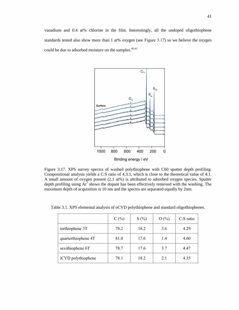
41
vanadium and 0.4 at% chlorine in the film. Interestingly, all the undoped oligothiophene
standards tested also show more than 1 at% oxygen (see Figure 3.17) so we believe the oxygen
could be due to adsorbed moisture on the samples.40,41
Figure 3.17. XPS survey spectra of washed polythiophene with C60 sputter depth profiling.
Compositional analysis yields a C:S ratio of 4.3:1, which is close to the theoretical value of 4:1.
A small amount of oxygen present (2.1 at%) is attributed to adsorbed oxygen species. Sputter
depth profiling using Ar+
shows the dopant has been effectively removed with the washing. The
maximum depth of acquisition is 10 nm and the spectra are separated equally by 2nm.
Table 3.1. XPS elemental analysis of oCVD polythiophene and standard oligothiophenes.
C (%) S (%) O (%) C:S ratio
terthiophene 3T 78.2 18.2 3.6 4.29
quarterthiophene 4T 81.0 17.6 1.4 4.60
sexithiophene 6T 78.7 17.6 3.7 4.47
iCVD polythiophene 78.1 18.2 2.1 4.35

42
Figure 3.18. High resolution (a) C1s and (b) S2p XPS spectra of washed polythiophene. Peak
fits reveal the expected 1:1 ratio of α and β carbons aswell as a single sulfur species of the
thiophene ring.
As shown in Figure 3.18, high resolution C1s XPS spectra were also taken to elucidate specific
chemical bonding environments. The C1s region was fitted with two peaks located at 284.6 and
285.4 eV that can be attributed to β and carbons of the thiophene ring, respectively.39,42
The
43
relative intensity of these two peaks is 0.95 (theoretical value = 1.0), which lends support that
the thiophene ring structure is preserved during oCVD and stoichiometric polythiophene is
obtained. The S2p peak was decomposed into its constituent 2p3/2 and 2p1/2 peaks with a known
band split of 1.19 eV and a relative intensity of 2:1. The single 2p3/2 sulfur peak at 163.5 eV
indicates that the sulfur environment in the washed sample is intact in the thiophene ring.38
3.7.3 UV-vis spectroscopy
The UV-vis spectra of as-deposited and washed polythiophene are given in Figure 3.19. The as-
deposited sample shows two broad absorptions at 450 and 690 nm that are typical of doped
polythiophene.43,44
With washing, the sample was dedoped and the spectrum now shows a single
prominent peak with a maximum at 480 nm. Thismax is comparable to the reported value for
polythiophene synthesized electrochemically and has been assigned to the π-π* transition.45-48
Basedontheonsetoftheπ-π*transition,theopticalbandgapisestimatedtobe1.9eV,whichis
similar to that reported for electrochemically synthesized polythiophene.45
It should be noted that
the washing in this case was done using chloroform instead of acid as we wanted to dissolve and
separate out any soluble fraction for UV-vis analysis as well. Interestingly, themax of the
soluble portion is observed at 418 nm, which is lower than the peak at 480 nm for the washed
solid fraction (Figure 3.20).
This shift can be related directly to a difference in conjugation length, as shown in Figure
3.21 where max for various undoped standard oligothiophenes is plotted against the number of
thiophene repeat units, and compared with the soluble and undissolved portions of the washed
polythiophene film. We clearly see with the oligothiophene standards that a higher peak
wavelength value, which indicates a greater conjugation length, correlates naturally to a longer

44
Figure 3.19. UV-vis spectra of as-deposited and washed polythiophene. The as-deposited film
shows the characteristic broad polaron absorption of the doped form while the dedoped film after
washing gives a single absorption peak at λmax =470nmoftheπ-π*transition.
Figure 3.20. UV-vis spectrum of the dissolved portion of PTh.

45
thiophene chain. Based on this trend, the soluble fraction is estimated to consist mainly of chain
oligomers of five thiophene units long while the washed polythiophene film is expected to be
much longer than six thiophene units given that its peak wavelength is much higher than all the
oligothiophene standards tested. In fact, it is higher than that reported for polybithiophene and
comparable to that of polythiophene synthesized electrochemically.48
Figure 3.21. Correlation of λmax with the number of thiophene chain units, comparing literature
data49
and experimental data of undoped standard oligothiophenes with washed polythiophene
and its dissolved soluble fraction after washing. The correlation indicates a longer conjugation
length with a higher degree of polymerization. The correlation also indicates that the solid
portion of the washed film is much longer than 6-7 thiophene units while the dissolved fraction
consists mainly of 5 repeat units.
3.7.4 Cyclic voltammetry
A cyclic voltammetry sweep of the acid washed polythiophene film between –0.2 and 1.2 V vs.
the saturated calomel electrode (SCE) is shown in Figure 3.22. The anodic and cathodic peaks
observed at 1.1 and 0.6 V, respectively, are in good agreement with reported data for
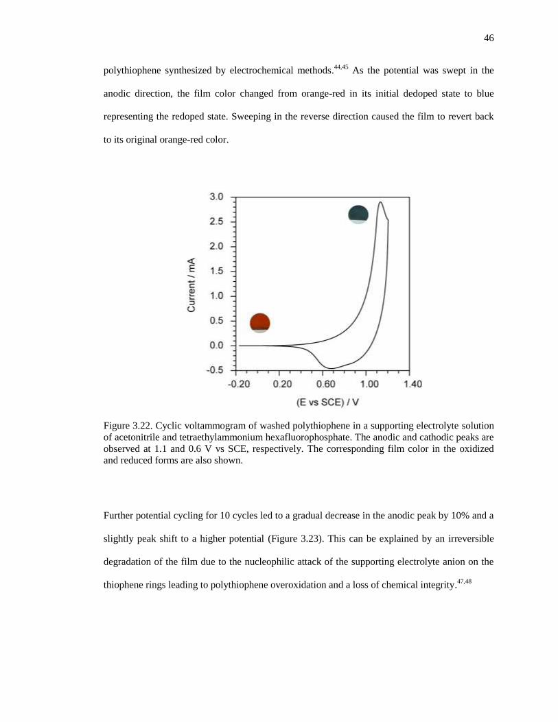
46
polythiophene synthesized by electrochemical methods.44,45
As the potential was swept in the
anodic direction, the film color changed from orange-red in its initial dedoped state to blue
representing the redoped state. Sweeping in the reverse direction caused the film to revert back
to its original orange-red color.
Figure 3.22. Cyclic voltammogram of washed polythiophene in a supporting electrolyte solution
of acetonitrile and tetraethylammonium hexafluorophosphate. The anodic and cathodic peaks are
observed at 1.1 and 0.6 V vs SCE, respectively. The corresponding film color in the oxidized
and reduced forms are also shown.
Further potential cycling for 10 cycles led to a gradual decrease in the anodic peak by 10% and a
slightly peak shift to a higher potential (Figure 3.23). This can be explained by an irreversible
degradation of the film due to the nucleophilic attack of the supporting electrolyte anion on the
thiophene rings leading to polythiophene overoxidation and a loss of chemical integrity.47,48

47
Figure 3.23. Cyclic voltammetry sweep of PTh.
3.7.5 Effect of oCVD processing conditions on polymer properties
To investigate the effect of oCVD synthesis and process parameters on resulting film properties,
we relied on the relative pressure Pr/Pr,sat (where Pr is the partial pressure of the reactant species
and Pr,sat is its vapor pressure at the substrate temperature) as a key adsorption parameter for
controlling the surface concentration of monomer (M) and initiator (I), and in turn the
polymerization growth kinetics during deposition.50
For the studies here, the substrate
concentration was kept constant at 5 °C, which yielded a monomer and initiator vapor pressure
of 27 and 7 torr, respectively, based on literature vapor-liquid equilibrium data.51
Then by
changing the flow rate of the reactants, we were able to design a series of synthesis experiments
to explore the oCVD space for influencing polymer film characteristics. Table 3.2 shows
polythiophene synthesized by oCVD at various (PM/PM,sat, PI/PI,sat) coordinates i.e., at different
surface monomer and initiator concentrations, and the corresponding electrical conductivity of

48
the as-deposited films. Although the values lie in the lower range reported for polythiophene,29
more importantly, conductivity can be controlled by tuning iCVD synthesis. In addition, Table
3.2 gives the corresponding Raman intensity ratio 1 / 2 of the as-deposited polythiophene as
well as the UV-vis absorption peak max of the washed polythiophene.
Qualitatively, we can see from sample runs 1-3 in which monomer concentration was kept
roughly constant while initiator concentration was increased that the UV-vis absorption peak
shifted to lower wavelengths. From our discussion of Figure 3.21, this shift indicates a decrease
in polythiophene chain length and since the UV-vispeakcorrespondstotheπ-π*transition,itis
reasonable to expect that this also means a shorter conjugation length. Likewise, comparing
sample runs 3 and 5, for a similar initiator concentration, a decrease in monomer concentration
also resulted in a decrease in peak wavelength and effective conjugation length. These
observations suggest that a greater presence of monomer relative to the initiator at the growth
surface leads to a greater conjugation length of the deposited polythiophene. However, this
generalization does not fully explain the results. If we compare runs 2 and 4 in which the relative
amount of monomer to initiator is the same, we do not get the same absorption maximum. In
addition, the max values do not fully correlate with the observed conductivities even though the
peakrepresentsaπ-π*transition.Thiscanberationalizedbyrealizing thatthe max data only
represents washed polythiophene in which the dopant has been removed. In addition, the
washing also removed the soluble oligothiophene portion of the polymer. Thus, we should not
expect the max data to fully follow the conductivity data of the as-deposited polythiophene.

49
Table 3.2. Effect of oCVD synthesis conditions on polythiophene properties.Sample run.
PM/PM,sat PI/PI,sat λmaxa (nm) I(ν1)/I(ν2) Conductivity
(mS/cm)
1 0.55 0.10 490 0.28 6.2
2 0.53 0.53 480 0.26 4.0
3 0.50 0.73 472 0.32 20.1
4 0.25 0.25 460 0.21 0.71
5 0.15 0.78 445 0.20 NAb
a λmax obtained from the washed film
b No stable reading.
To fully rationalize the observed data, we should recognize that the oxidant utilized in
oCVD synthesis acts not only as an initiator to enable the polymerization of polythiophene but
also simultaneously dopes the formed polymer. As such, the absolute amount of initiator is
equally important in determining electrical conductivity. Thus, looking at runs 2 and 4 again,
with more initiator present a higher electrical conductivity is observed even though the relative
amounts of monomer and initiator are equivalent in the two runs. Quantitatively, we have found
that the Raman intensity ratio 1 / 2 correlates well with film conductivity, noting that both sets
of measurements were taken from as-deposited polythiophene. The larger the 1 / 2 intensity
ratio, the higher the film conductivity. This phenomena observed by others for VVP and
attributed to the lower chain length which suggest less conformational defect in the chain and
suggest higher conjugation length in the doped film.32
So a combination of sufficient chain
length, effective conjugation length and effective doping in the as deposited film resulted in the
observed behavior. It is worth mentioning that our results along with other reports on the values

50
of the π-π*suggests that the saturation limit for wavelength of this transition is not necessary
471 nm and can exceed this value.45
This observation pose that effective conjugation length in
the polythiophene system is smaller than what is predicted (17 units) with the nonlinear
approach introduced by Meier et al.52
It is widely recognized that the synthesis of polythiophene in the liquid phase using an
oxidant initiator follows an oxidative polymerization mechanism.54
In a vapor deposition
environment, the oxidative polymerization mechanism has also been suggested for the synthesis
of PEDOT.1,54
Here we propose that the polymerization of polythiophene using vanadium
oxytrichloride as the oxidant initiator follows a similar scheme whereby a cation radical is
formed on the thiophene ring and stabilized by vanadium compound counteranions acting as the
dopant. This enables the addition of thiophene rings through - carbon coupling and allows the
formation of extended conjugation. The specificity of this coupling is supported by our test of
using 2,5-dibromothiophene with a comparable oxidation potential as the thiophene monomer
but which did not result in any film formation at least in the wide oCVD parameter space that
was explored here. However, the possibility of - and - linkages during polymerization
cannot be unequivocally ruled out at this point. It is possible that the presence of these defects
could account for the lower electrical conductivity of the polythiophene films particularly when
they were deposited at a high initiator concentration relative to the monomer.55
One hypothesis is
that the higher initiator concentration at low monomer surface coverage simply provides more
active initiator species that can attack the less reactive β sites, leading to a greater probability of
structural defect linkages being formed. Unfortunately, Raman spectroscopy was not sensitive
enough to detect these vibrational defect modes. However, by re-examining the FTIR spectra,
we have found that the peak intensity ratio of the C–H bending vibrations at 690 and 790 cm-1
,
which has been correlated with chain length,26
actually underestimated the chain length predicted

51
by UV-vis. This weakening in the C–H vibration modes could be an indication of defects, and in
fact has been observed in the electrochemical synthesis of polythiophene and introduced as a
reason for lower polythiophene conductivity.55
3.8 Conclusions
Polymer electrolyte with exceptionally clean and accurate stoichiometry were synthesized using
iCVD. The polymer ionic conductivity was measured and optimized for the gel electrolyte
application. The polymer was fully characterized and the molecular weight found to be in a
suitable range for gel electrolyte application. Despite having exceptional electroactive properties,
applications of unsubstituted polythiophene have been limited due to its insolubility. Here we
showed for the first time that the unsubstituted polythiophene can be deposited through oCVD
process using vanadium oxytrichloride as an effective oxidant. The deposited films were well
characterized and the control over polymer properties in the space parameter of the oCVD
obtained. Vibrational spectroscopy along with the conductivity results and UV-vis data suggest
that the deposited film is not fully doped polymer. The possibility of - and - linkages
during polymerization cannot be unequivocally ruled out at this point. It is possible that the
presence of these defects could account for the lower electrical conductivity of the
polythiophene films particularly when they were deposited at a high initiator concentration
relative to the monomer. However, the route of this defect could not be in chemical degradation
of the ring as XPS did not indicate any chemical change in the ring structure. Significantly,
polymer conjugation length and electrical conductivity can be tuned by controlling oCVD
process variables. Polymerization is found to be adsorption-limited so by providing sufficient
monomer and limiting the amount of initiator at the growth surface, polythiophene is believed to
be formed through - thiophene linkages.

52
3.9 References
1. J. P. Lock, S. G. Im and K. K. Gleason, Macromolecules, 2006, 39, 5326-5329.
2. B. Winther-Jensen, J. Chen, K. West and G. Wallace, Macromolecules, 2004, 37, 5930-
5935.
3. Y.H. Liao, D.Y. Zhou, M.-M. Rao and W.S. Li, Dianchi Gongye, 2008, 13, 428-432.
4. H. Yang, M. Huang, J. Wu, Z. Lan, S. Hao and J. Lin, Materials Chemistry and Physics,
2008, 110, 38-42.
5. A. A. Argun, A. Cirpan and J. R. Reynolds, Advanced Materials, 2003, 15, 1338-1341.
6. R. K. Bose and K. K. S. Lau, Biomacromolecules, 2010, 11, 2116-2122.
7. C. Longo, A. F. Nogueira, M.-A. De Paoli and H. Cachet, Journal of Physical Chemistry
B, 2002, 106, 5925-5930.
8. K. Chan and K. K. Gleason, Langmuir, 2005, 21, 8930-8939.
9. G. P. López, D. G. Castner, B. D. Ratner, Surface and Interface Analysis, 1991 17, ( 5),
267–272.
10. K. K. S. Lau and K. K. Gleason, Macromolecules, 2006, 39, 3695-3703.
11. Bard, A. J.; Faulkner, L. R., Electrochemical Methods: Fundamentals and Applications.
Wiley, Hoboken, USA 2000.
12. Barsoukov, E.; Macdonald, J. R., Impedance Spectroscopy: Theory, Experiment, and
Applications. Wiley, Hoboken, USA 2005.
13. R. Komiya, L. Y. Han, R. Yamanaka, A. Islam and T. Mitate, Journal of Photochemistry
and Photobiology, A, 2004, 164, 123-127.
14. C. Li, H. Bai and G. Shi, Chemical Society Reviews, 2009, 38, 2397-2409.
15. T. Yamamoto, K. Sanechika and A. Yamamoto, Journal of Polymer Science: Polymer
Letters, 1980, 18, 9-12.
53
16. J. W. P. Lin and L. P. Dudek, Journal of Polymer Science: Polymer Chemistry 2003, 18,
2869-2873.
17. W. T. Robinson and B. Belleau, Journal of the American Chemical Society, 1972, 94,
4376-4378.
18. Kobayashi, M.; Chen, J.; Chung, T. C.; Moraes, F.; Heeger, A. J.; Wudl, F. Synthetic
Metals 1984, 9, (1), 77-86.
19. T. Yamamoto, A. Morita, Y. Miyazaki, T. Maruyama, H. Wakayama, Z. H. Zhou, Y.
Nakamura, T. Kanbara, S. Sasaki and K. Kubota, Macromolecules, 1992, 25, 1214-
1223.
20. K. Yoshino, S. Hayashi and R.i. Sugimoto, Japanese Journal of Applied Physics, 1984,
23, 899-900.
21. R. Sugimoto, S. Takeda, H. B. Gu and K. Yoshino, Chemistry Express, 1986, 1, 635-
638.
22. O. Inganäs, W. R. Salaneck, J. E. Österholm and J. Laakso, Synthetic Metals, 1988, 22,
395-406.
23. J. R. Reynolds, J. P. Ruiz, A. D. Child, K. Nayak and D. S. Marynick, Macromolecules,
1991, 24, 678-687.
24. S. Nejati and K. K. S. Lau, Nano Letters, 2011, 11, 419-423.
25. S. Hotta, W. Shimotsuma and M. Taketani, Synthetic Metals, 1984, 10, 85-94.
26. Y. Furukawa, M. Akimoto and I. Harada, Synthetic Metals, 1987, 18, 151-156.
27. R. D. Gaussian 03, M. J. Frisch, G. W. Trucks, H. B. Schlegel, G. E. Scuseria, M. A.
Robb, J. R. Cheeseman, J. A. Montgomery, Jr., T. Vreven, K. N. Kudin, J. C. Burant, J.
M. Millam, S. S. Iyengar, J. Tomasi, V. Barone, B. Mennucci, M. Cossi, G. Scalmani,
N. Rega, G. A. Petersson, H. Nakatsuji, M. Hada, M. Ehara, K. Toyota, R. Fukuda, J.
Hasegawa, M. Ishida, T. Nakajima, Y. Honda, O. Kitao, H. Nakai, M. Klene, X. Li, J. E.
Knox, H. P. Hratchian, J. B. Cross, V. Bakken, C. Adamo, J. Jaramillo, R. Gomperts, R.
E. Stratmann, O. Yazyev, A. J. Austin, R. Cammi, C. Pomelli, J. W. Ochterski, P. Y.
Ayala, K. Morokuma, G. A. Voth, P. Salvador, J. J. Dannenberg, V. G. Zakrzewski, S.
Dapprich, A. D. Daniels, M. C. Strain, O. Farkas, D. K. Malick, A. D. Rabuck, K.
Raghavachari, J. B. Foresman, J. V. Ortiz, Q. Cui, A. G. Baboul, S. Clifford, J.
Cioslowski, B. B. Stefanov, G. Liu, A. Liashenko, P. Piskorz, I. Komaromi, R. L.
Martin, D. J. Fox, T. Keith, M. A. Al-Laham, C. Y. Peng, A. Nanayakkara, M.

54
Challacombe, P. M. W. Gill, B. Johnson, W. Chen, M. W. Wong, C. Gonzalez, and J. A.
Pople, Gaussian, Inc., Wallingford CT, 2004.
28. G. Rauhut and P. Pulay, Journal of Physical Chemistry, 1995, 99, 3093-3100.
29. M. Akimoto, Y. Furukawa, H. Takeuchi, I. Harada, Y. Soma and M. Soma, Synthetic
metals, 1986, 15, 353-358.
30. E. A. Bazzaoui, J. Aubard, N. Félidj, G. Laurent and G. Lévi, Journal of Raman
Spectroscopy, 2005, 36, 817-833.
31. G. Poussigue, C. Benoit, J. L. Sauvajol, J. P. Lere-Porte and C. Chorro, Journal of
Physics: Condensed Matter, 1991, 3, 8803-8824.
32. P. M. Bayley, B. Winther-Jensen, D. R. MacFarlane, N. M. Rocher and M. Forsyth,
Reactive Functional Polymers, 2008, 68, 1119-1126.
33. G. Compagnini, A. De Bonis, R. S. Cataliotti and G. Marletta, Physical Chemistry
Chemical Physics, 2000, 2, 5298-5301.
34. C. Castiglioni, M. Del Zoppo and G. Zerbi, Journal of Raman Spectroscopy, 2005, 24,
485-494.
35. E. Bazzaoui, G. Levi, S. Aeiyach, J. Aubard, J. Marsault and P. Lacaze, Journal of
Physical Chemistry, 1995, 99, 6628-6634.
36. E. A. Bazzaoui, S. Aeiyach, J. Aubard, N. Felidj, P. C. Lacaze, N. Sakmeche and G.
Lévi, Journal of Raman Spectroscopy, 1998, 29, 177-183.
37. G. Tourillon and Y. Jugnet, Journal of Chemical Physics, 1988, 89, 1905-1913.
38. E. T. Kang, K. G. Neoh and K. L. Tan, Physical Reviews B, 1991, 44, 10461-10467.
39. L. Atanasoska, K. Naoi and W. H. Smyrl, Chemistry of. Materials, 1992, 4, 988-994.
40. H. Hintz, H. Peisert, H. J. Egelhaaf and T. Chassé, Journal of Physical Chemistry C,
2011, 115, 13373-13376.
41. D. Oeter, C. Ziegler and W. Göpel, Synthetic Metals, 1993, 61, 147-150.
42. S. S. Jeon, S. J. Yang, K. J. Lee and S. S. Im, Polymer, 2010, 51, 4069-4076.
55
43. G. Zotti and G. Schiavon, Synthetic Metals, 1989, 31, 347-357.
44. D. Zhang, J. Qin and G. Xue, Synthetic Metals, 1999, 106, 161-164.
45. S. Alkan, C. A. Cutler and J. R. Reynolds, Advanced Functional Materials, 2003, 13,
331-336.
46. H. Harada, T. Fuchigami and T. Nonaka, Journal of Electroanalytical Chemistry, 1991,
303, 139-145.
47. J. Roncali, F. Garnier, M. Lemaire and R. Garreau, Synthetic Metals, 1986, 15, 323-331.
48. S. Wang, K. Tanaka and T. Yamabe, Synthetic Metals, 1989, 32, 141-150.
49. I. F. Perepichka and D. F. Perepichka, Handbook of Thiophene-Based Materials, Wiley,
Chichester, UK, 2009.
50. K. K. S. Lau and K. K. Gleason, Macromolecules, 2006, 39, 3688-3694.
51. C. L. Yaws, Yaw's Handbook of Antoine Coefficients for Vapor Pressure, Knovel,
2009.
52. H. Meier, U. Stalmach and H. Kolshorn, Acta Polymerica, 1997, 48, 379-384.
53. S. Sadki, P. Schottland, N. Brodie and G. Sabouraud, Chemical Society Reviews, 2000,
29, 283-293.
54. S. G. Im, P. J. Yoo, P. T. Hammond and K. K. Gleason, Advanced. Materials, 2007, 19,
2863.
55. K. Tanaka, T. Shichiri and T. Yamabe, Synthetic Metals, 1986, 16, 207-214.

56
4 Chapter 4: Integration of Polymer Electrolytes in Dye Sensitized Solar Cells
4.1 Introduction
The global demand for energy is increasing with population and for the major portion of this
demand we are currently relying on fossil fuel. The increase in green house gases associated
with burning fossil fuel and the dwindling fossil fuel supply have fueled attention to other
sources of energy that are cleaner.1
Photovoltaic (PV) devices which rely on abundant sun
energy are among the promising energy conversion devices for the future of the planet. However
due to the higher cost of solar cells for energy conversion and delivery this technology has not
been fully exploited. Having more economical PV cells with respectable efficiency that can last
for 20 years or more could be a way to bring this technology to reality. Consequently, the quest
for making current PV technologies cheaper has led to many inventions in the last 20 years
among which the dye sensitized solar cell (DSCC) has evolved quite rapidly to a point that it is
currently undergoing commercialization.2 The dye sensitized solar cell first introduced by
Michael Grätzel and Brian O’Regan in 1992 has gone through many refinements and
efficiencies have exceeded 11%.3 Lately, devices in the lab scale with efficiency as high as
12.3% have been fabricated and it appears that the efficiency of this sophisticated design can
reach upward of 15%.4,5
A higher efficiency DSSC certainly will help pave the road for more extensive
commercialization of this technology, there remains challenges left to be addressed for
enhancing the performance of the cell and modules. The first and most important problem
associated with the cell design is leakage of the liquid electrolyte at elevated temperature which
has detrimental effect on cell performance and eventually results in cell failure.6 Significant
attention has been devoted to this problem and many materials, including organic and inorganic
solid state hole transport materials,7-9
conjugated polymers,10,11
and solid and gel polymer

57
electrolytes,12-15
have been explored to replace the liquid electrolyte. Among these choices,
polymer electrolytes are a promising candidate as they can be designed towards enhancing ionic
conductivity.16
Nevertheless the effort to integrate polymer within the cell has been less than
effective and polymer infiltration is constrained by the high aspect ratio of the mesoporous
nanostructured electrode.17-20
To surmount this problem here we are relying on our unique
method to integrate polymer materials within the nanostructures.
.
4.1.1 DSSC working principle
As shown in Figure.4.1, a DSSC is composed of five main components: a transparent conductive
oxide (TCO) electrode, a wide band gap semiconductor, a chromophore sensitizer, a hole
conductor media, and a counter electrode to complete the circuit.
Figure.4.1. Dye sensitized solar cell layout.

58
To benefit from a higher surface area and more dye incorporation in the semiconductor
layer, the electrode is fabricated as a porous network of interconnected nanoparticles with
electrode roughness (the ratio of actual available surface area to geometric surface area) as high
as 1000. To form these types of electrode, a sol-gel process is being employed using
nanoparticles of a semiconductor with nominal particle size from 15-25 nm that results in 45-
75% porosity.18,21,22
Currently, TiO2 in the anatase form is being used for electrode fabrication
and the specific surface area ranging from 55-150 m2/g depending on the size of the particle used
is obtained. Upon illumination, the ground state of the dye is excited to its unrelaxed metal-to-
ligand-charge-transfer (MLCT) state. The molecule can relax to its original state within tens of
femto to a pico second or can inject an electron into the semiconductor from any of the
unthermalized states.23
The electrons injected into the semiconductor are transferred within the
network of TiO2 through a random walk assisted by transfer between localized sites which are
distributed in energy or tunneling over a longer range.24
These electrons find their way to the
conductive substrate on which the electrode assembly is fabricated. The dye in the oxidize form
on the other hand is being reduced by a redox couple in the electrolyte solution. In the typical
DSSC, iodide and triiodidie are the redox species in the electrolyte.25
The way the redox species
works in the system is that the I– will donate an electron to regenerate the dye and form I3
–. The
I3– diffuse to the platinum interface at the counter electrode where it receives back electrons from
the external circuit in a two electron transfer to reform I–. In this way, the photogenerated
electrons from the dye traveling through the external circuit can continuously be created by the
regeneration of the dye.
However, the electrons injected into the semiconductor diffuse within TiO2 structure can
recombine with the ionic species in the solution at the semiconductor-liquid electrolyte interface.
Different mechanisms have been proposed for this recombination processes and the detail of

59
possible mechanism can be found elsewhere.22,26,27
Recombination can also occur by the
recombination of the electron in the TiO2 network with the dye but this pathway is of lesser
importance and has been often being ignored in most studies as it is insignificant compared to
recombination with the redox ions in the electrolyte.28
4.1.2 Replacing the liquid electrolyte
As mentioned earlier, the medium for idodide/triiodide transport is a liquid electrolyte which in
this case is an aprotic solvent, and the most commonly used in DSSC is acetonitrile. It is known
that the acetonitrile can escape the cell and cause cell failure. This effect is exacerbated at higher
temperature and has led many researchers to find alternatives.6 To replace the liquid with a solid
material which potentially eliminates the problem associated with leaking, many attempts had
been made to infiltrate polymers and solid state hole transport materials.17,25
Although the
importance of pore filling and pore wetting is recognized as a necessary technological leap for
advancing DSSC performance, currently the effective electrode thickness of the device
fabricated with these materials has been limited by their penetration depth into the mesoporous
TiO2 layer to ~2 µm.16-18
The nanoscale pore diameter and narrow pore structure make it
especially difficult for liquid based techniques to transport these materials due to viscous and
steric effects. In addition, these processes introduce solvents into the system that make their
complete removal nontrivial, and the presence of any unwanted chemical will most likely
deteriorate cell performance.
4.1.3 Pore filling methodology
iCVD was used to polymerize poly(2-hydroxyethyl methacrylate) (PHEMA) as a potential
polymer electrolyte material inside the mesoporous TiO2 electrode of the DSSC. PHEMA has

60
been chosen as the presence of the ester and hydroxyl groups are expected to facilitate ion
transport and enable the formation of a stable gel electrolyte with propylene carbonate and γ-
butyrolactone typically used as dielectrics in DSSCs.30
Using conventional free radical
polymerization of 2-hydroxyethyl methacrylate (HEMA) and t-amyl peroxide (TAPO) as the
monomer and initiator, respectively, the effect of critical iCVD parameters in influencing the
rate of polymer formation inside the pores has been investigated in order to obtain a systematic
way for filling the mesoscopic TiO2 electrode effectively. Figure 4.2 shows the iCVD scheme to
integrate polymer electrolyte within the mesoporous electrode structure. To obtain pore filling of
the mesoporous TiO2 electrode with PHEMA, we performed iCVD on 3-4 µm thick electrode
layers to systematically investigate different iCVD parameters and observe the resulting
electrode SEM cross sections.
Figure 4.2. Schematic of the pore filling process during initiated chemical vapor deposition
(iCVD). Monomer (M) and initiator (I) molecules are delivered into the reaction chamber in the
form of gaseous vapors. The initiator is selectively activated by a series of heated filaments. The
activated initiator (R) and monomer (M) adsorb onto the TiO2 surface within the nanostructured
mesoporous electrode that is kept cooled to enhance the adsorption-limited process. Addition
polymerization of the monomer at activated initiator sites results in the formation of a growing
polymer inside the pores.

61
4.2 Experimental
4.2.1 Electrode preparation
The titanium dioxide colloidal paste consisting of TiO2 nanoparticles P25 (Envonik) was
prepared using a published procedure.31
The prepared paste was spin coated at 700-1200 rpm
ontofluorinedopedtinoxideconductiveglass(HartfordGlass,15Ω/) to obtain a film of the
paste between 2 and 8 µm in thickness. To create the mesoporous structure, the spin coated TiO2
paste was heated up to 500°C and annealed for 30 min. For pore filling experiments, samples
were cooled to room temperature and stored until further use. For dye sensitized solar cell
fabrication, samples were cooled down to 100 °C and immersed in a 3x10⁻⁴
M solution of
photosensitizer dye cis-dicyano-bis(2,2’-bipyridyl-4,4’-dicarboxylic acid) ruthenium(II)
(Ruthenizer 505, Solaronix) or cis-bis(isothiocyanato)bis(2,2'-bipyridyl-4,4'-dicarboxylato)-
ruthenium(II) (Ruthenizer 535, Solaronix) in pure ethanol, and left in the dark for 20 h.
4.2.2 Pore filling
Each prepared mesoporous TiO2 on glass was first heated up to 200 °C for 30 min to remove any
adsorbed water or contamination inside the pores and after cooling the sample was then placed
inside our iCVD chamber to enable polymerization of poly(2-hydroxyethyl methacrylate)
(PHEMA) inside the mesoporous TiO2. Briefly, the chamber was evacuated to a base pressure of
< 7 mtorr using a dry pump system (Edwards iH160). The monomer, 2-hydroxyethyl
methacrylate (Aldrich, 97%) and initiator and t-amyl peroxide (Aldrich, 97%) were used as
received, and metered independently at set flow rates through precision needle valves
(Swagelok) into the chamber. The chamber pressure was controlled by a downstream throttle
valve (MKS instruments 253B) and a pressure transducer (MKS instruments 626A) connected to
a pressure controller (MKS instruments 651C). The substrate temperature of the sample was kept

62
constant through backside cooling water controlled with a recirculating chiller (Neslab RTE-7).
A series of equally spaced Chromaloy filaments (Goodfellow) was suspended above the sample
and resistively heated using a DC power supply (Sorensen DLM 60-10) to thermally activate the
initiator. With the cooling water and filament temperatures at 27 and 350 °C, respectively, the
substrate temperature was measured to be 50 °C. To investigate the iCVD parameter space for
pore filling, the monomer and initiator flow rates were set at different values from 0.2 to 0.8
sccm (std cm3
per min), and the chamber was maintained at pressures in the range of 60 to 200
mtorr. After iCVD polymerization and deposition was completed, the chamber was pumped
down while a stream of argon was introduced to purge the reactor until base pressure was
restored. The chamber was then vented to atmosphere and the sample was removed for
characterization with cross sectional SEM (Zeiss Supra 50 VP) after a ~5 nm Pt/Pd coating to
evaluate the degree of pore filling.
4.2.3 Pore filing estimation
Each sample was cleaved into two parts, one part was used for cross sectional SEM and the
remainder was used for thermogravimetric analysis (TGA). Using cross sectional SEM, the
polymer overlayer coating and the mesoporous thickness were measured at 5 different locations
along the edge and the average values used for pore filling estimation. TGA was performed on a
Q50 (TA Instruments) with a 10°C/min ramp from room temperature to 800 °C under a nitrogen
purge.. The porosity of the starting unfilled electrode was estimated using N2 adsorption
isotherm at 77 K. The mesoporous TiO2 deposited on a silicon substrate was first placed into a
macro cell (Quantachrome) and degassed at 180 °C for 12 h. The cell was then connected to the
Autosorb-1 (Quantachrome) and adsorption/desorption isotherms were recorded in between 5
and 100% of P/P0 where P0 was set to 760 torr.

63
4.2.4 Dye sensitized solar cell fabrication
Each prepared TiO2 electrode was removed from the dye solution in an enclosed argon
environment and rinsed thoroughly with pure ethanol to remove any excess and unadsorbed dye
from the TiO2 surface. The sample was then transferred immediately to the iCVD reactor for
incorporating PHEMA with the procedure described above and using iCVD conditions that gave
complete pore filling. After deposition, the sample was removed from the chamber, and some of
the deposited polymer were removed from the glass edge with a cotton swab dipped in dimethyl
formamide (EMD Chemicals, >99.9%) to create the electrical contact. To incorporate the redox
couple in the PHEMA, the sample was immersed for 6 h in a redox solution composed of 0.5 M
lithium iodide (Aldrich, 99.9%) and 0.05 M iodine (Aldrich, 99%) in 50:50 or 0:100 vol% of γ-
butyrolactone (Aldrich, >99%) and propylene carbonate (Aldrich, >99%). A platinized counter
electrode was prepared by spin coating of 50 µl of 5 mM solution of chloroplatinic acid hydrate
(Aldrich, 99.9%) in 2-propanol(Aldrich,99%)onFTOglass(HartfordGlass,15Ω/) followed
by annealing at 400 °C for 40 min. The counter electrode and photoanode were pressed against
each other and clipped together. Comparisons were made with a standard liquid electrolyte cell
prepared in the same way except that the polymer was replaced by acetonitrile (Alfa Aesar,
99.7%), which was used as the redox solvent and electrolyte, and two L-shaped spacers (Surlyn,
Solaronix) were heat-sealed between the two electrodes to avoid a short in the cell. The distance
between the two electrodes is measured to be 25 µm.
4.2.5 Solar cell characterization
Photovoltaic measurements of each assembled DSSC was carried out in a custom solar simulator
equipped with a 300 W Xe lamp filtered to AM 1.5 spectral conditions. Data were taken using a
Gamry Reference 600 with a 0.26 cm2 mask on the samples under 100 mW/cm
2 irradiance and
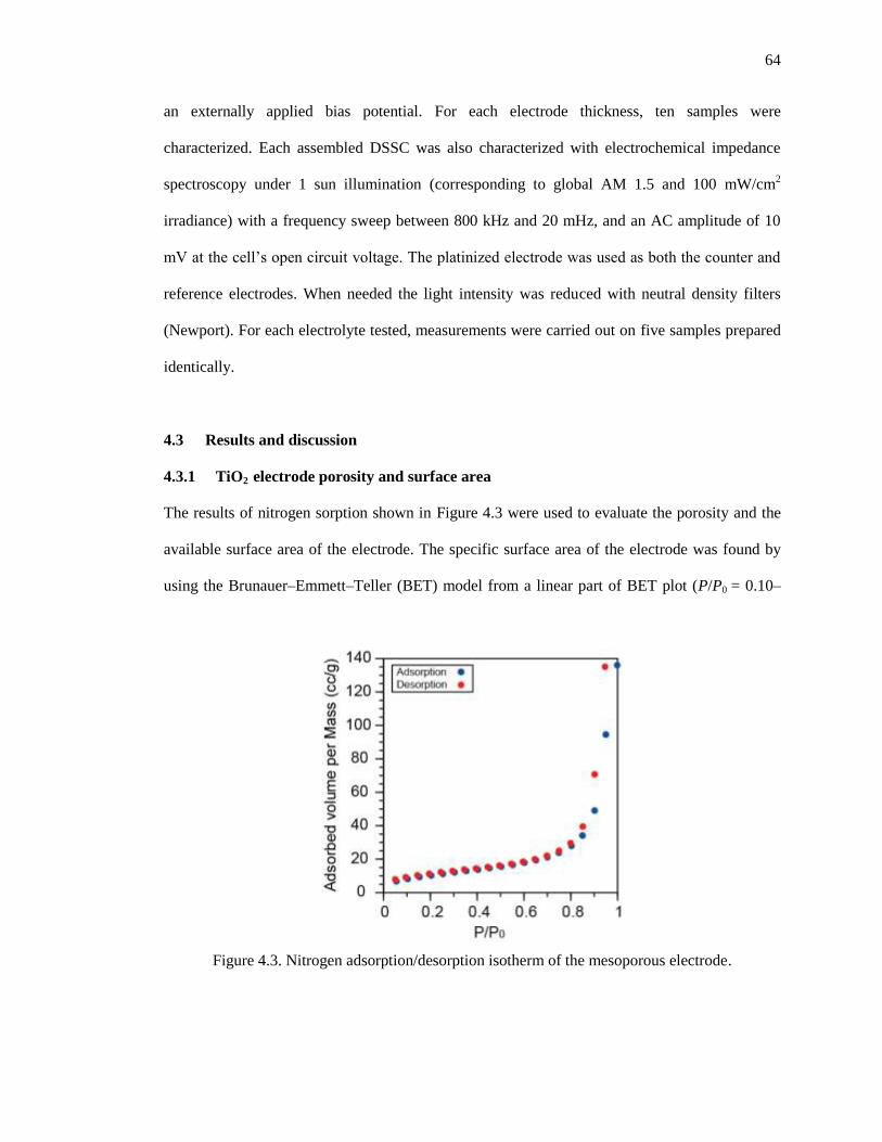
64
an externally applied bias potential. For each electrode thickness, ten samples were
characterized. Each assembled DSSC was also characterized with electrochemical impedance
spectroscopy under 1 sun illumination (corresponding to global AM 1.5 and 100 mW/cm2
irradiance) with a frequency sweep between 800 kHz and 20 mHz, and an AC amplitude of 10
mVatthecell’sopencircuitvoltage.Theplatinizedelectrodewasusedasboththecounterand
reference electrodes. When needed the light intensity was reduced with neutral density filters
(Newport). For each electrolyte tested, measurements were carried out on five samples prepared
identically.
4.3 Results and discussion
4.3.1 TiO2 electrode porosity and surface area
The results of nitrogen sorption shown in Figure 4.3 were used to evaluate the porosity and the
available surface area of the electrode. The specific surface area of the electrode was found by
using the Brunauer–Emmett–Teller (BET) model from a linear part of BET plot (P/P0 = 0.10–
Figure 4.3. Nitrogen adsorption/desorption isotherm of the mesoporous electrode.

65
0.30) to be 55 m2/g, and average pore diameter was calculated by the Barrett–Joyner–Halenda
(BJH) method from the desorption part of isotherm to be about 17 nm.32
The average pore size
evaluated from BJH analysis matches well with that estimated using SEM image and imageJ
software from top down images. The porosity, found to be around 42-45%. This value is close to
reported values elsewhere for mesoporous TiO2.33
4.3.2 Effect of process parameters on pore filling
To investigate pore filling in the nanostructured electrode, the influence of partial pressure of the
reactant and substrate temperature during iCVD were studied as these parameters are known to
determine reactant surface concentration through the relative pressure parameter, z = P/Psat,
where P is the reactant partial pressure and Psat is the reactant vapor pressure at the substrate
temperature.10
To see the effect of reactant surface concentration on the pore filling quality,
initially a set of experiments by changing the total reactor pressure in between from 60 to 200
mtorr was investigated. This was essentially done to see the effect of system pressure on the
amount of PHEMA polymer which has filled the pores during iCVD (all other conditions
remaining constant, with HEMA, TAPO and N2 flow rates each set at 0.4 sccm). Compared to a
clean cross section of mesoporous TiO2 before iCVD (Figure 4.4a), deposition at 60 mtorr yields
only a polymer coating forming on top of the electrode without any polymer being visible within
the porous network (Figure 4.4b). As total pressure increased above 80 mtorr, filling of the inner
pore volume starts taking place (not shown). At 125 mtorr, a completely pore filled cross section
together with a top overcoat is observed (Figure 4.4c). Further increase in total pressure to 200
mtorr results in the quality of fill deteriorating again, with evidence of partial filling within the
mesoporous layer and premature coating on top (Figure 4.4d).

66
Figure 4.4. Effect of total pressure on pore filling, showing cross sectional SEM of the 4 µm
thick TiO2 electrodes that are (a) uncoated, and after iCVD treatment at a total pressure of (b) 60,
(c) 125, and (d) 200 mtorr (scale bar=100 nm). Complete pore filling is observed at intermediate
pressures.
To separate the individual effects of monomer and initiator partial pressures on pore filling,
each reactant flow rate was varied while keeping the other constant and compensating with
nitrogen inert to maintain a constant total flow rate (1.2 sccm) at a fixed total pressure (125
mtorr). Considering the initiator, adjusting TAPO flow rate from 0.2 to 0.8 sccm reveals that
flows above 0.4 sccm give complete pore filling while lower flows yield partial filling with
greater filling fraction as flow increases (Figure 4.5c). This is to be expected since the initiator

67
contributes to the amount of initiated polymer chain radicals, and once sufficient initiator
concentration has been reached polymer growth becomes monomer limited. This trend has been
observed previously with iCVD polymerization of acrylate and methacrylate polymers.34-36
Likewise, considering the monomer, adjusting the flow rate between 0.2 and 0.6 sccm (while
keeping a fixed total flow of 1.2 sccm and total pressure of 125 mtorr) shows that the fill quality
initially improves with increasing monomer flow rate and after passing a fully filled state, pore
filling deteriorates again (Figure 4.5).
Figure 4.5. The individual effect of the initiator and monomer on pore filling of TiO2 electrodes,
showing lack of complete pore filling at initiator flow rates of (a) 0.2, and (b) 0.3 sccm, and at
monomer flow rates of (c) 0.2, and (d) 0.6 sccm (scale bar=200 nm). Complete pore filling is
observed at initiator flow rates of 0.4 sccm and higher, and at a monomer flow rate of 0.4 sccm.

68
This observation indicates that pore filling is much more sensitive to the monomer than the
initiator flow rate. As an important note, although the initiator and monomer flows and their gas
concentrations are comparable (which might suggest long chain polymer formation would not be
possible), the surface concentration based on surface adsorption of the initiator is actually much
lower than for the monomer due its higher vapor pressure (by a factor of 10). In addition, the
initiator is activated in the gas phase so we would expect only a fraction of the activated initiator
to actually reach the surface.
Thus, we attribute the observed complete pore filling at intermediate total pressures (Figure
4.4) to mainly the effect of the monomer. To explain this pore filling behavior, we consider the
process to be composed of three main steps: (1) diffusion of the reactants inside the mesoporous
structure; (2) adsorption and surface diffusion of the reactants; and (3) polymerization reaction at
the surface. Like all porous media, we expect mass transport and reaction kinetics to each play a
critical role in polymer growth inside the pores. Diffusion needs to take into account both gas
and surface diffusion. Under iCVD conditions in mesoporous TiO2, Knudsen diffusion
dominates gas phase transport (Knudsen number Kn=λ/dpore~104, where λ and dpore are estimated
to be 160 µm and 17 nm, respectively). Surface diffusion, on the other hand, requires an
understanding of the adsorption behavior within mesoporous materials, and experimental studies
have shown that surface diffusivity reaches a maximum at some intermediate surface coverage
of the adsorbate,33,34
a clue that this phenomenon might capture the observed trend in our work.
4.3.3 Understanding pore filling dynamics
To understand the observed behavior of the monomer on pore filling, the fate of the monomer
during iCVD must be considered. Monomer is transported from the gas phase within the
mesoporous TiO2 structure to the TiO2 surface, where it adsorbs and then reacts. Thus, monomer

69
diffusion both in the gas phase and on the surface as well as monomer reaction at the surface has
to be taken into account. Our hypothesis is that complete pore filling will require surface
reaction to be rate limiting i.e., diffusional transport resistance is small. To determine whether
this is the case, the time constants for diffusion (τD) and reaction (τR) have been determined as a
function of monomer relative pressure z, as shown in Figure 4.6. The time constants give a
relative measure of how fast each process is taking place at different monomer surface
concentrations. The diffusion time constant is estimated as follows:
τD 2
eff
(4-1)
where L is the mesoporous TiO2 layer thickness and Deff is the effective diffusivity of the
monomer that accounts for both gas phase and surface diffusion acting as parallel resistances to
transport:
eff g k s s (4-2)
where Dk and Ds are the monomer diffusion coefficients in the gas phase and on the surface,
respectively, and pg and ps are the fractions of the monomer occupying the gas phase and
surface, respectively. Interestingly, experimental data on diffusion into micro- and mesoporous
media have shown a maximum diffusivity at the intermediate partial pressures or surface
coverage. This phenomenon has been well reported in detailed reviews37
and attempts have been
made to model this behavior,38,39
which we have adopted here to calculate the transport
parameters:
k pore3
1 α
(4-3)
s 0 1 F
2
F
(4-4)
α ad
pore
= F
pore
(4-5)

70
F
1
(4-6)
g 1 αα
g s
(4-7)
s 1 g (4-8)
Here, Dk is the Knudsen diffusion coefficient since gas phase diffusion inside mesoporous
TiO2 is found to be dominated by Knudsen diffusion (Kn = λ/dpore ~ 104, where λ and dpore are
estimated as 160 µm and 17 nm respectively). The Knudsen diffusivity has been corrected by a
(1 − α) term to account for the decrease in pore size with adsorption, where α is the ratio of the
volume of monomer adsorbed relative to the entire pore volume available. To estimate α we
used α = ( FLVml)/Vpore, where Vpore is the total pore volume, Vml is the volume of a monolayer of
the adsorbed monomer, and FL is the surface coverage that is based on the generalized
Freundlich isotherm appropriate for less than a monolayer adsorption and thus applies to the low
z values of the iCVD conditions used here. Based on similar diffusion in mesoporous structures,
the isotherm parameters are taken as m = 0.2 and K = 3,40
and 0 is estimated to be 4.6x10
-5
cm2/s.
37 In addition, monomer (HEMA) properties used are: molecular weight MW = 130.14
g/mol, liquid density s = 1.071 g/cm3, and gas density g that is derived from the ideal gas law
and is a function of z. Here, T is the mesoporous layer temperature of 50 °C. At this temperature,
the reaction time constant is calculated as:
τR 1
p M (4-9)
where kp is the second order propagation reaction rate constant for HEMA polymerization
(reported as 2527 L/mol.s at 50 °C41
), and [M] = s FL/MW is the monomer surface concentration,
which is a function of z and calculated based on a similar reported approach.36
Now plotting τD
and τR as a function of z (Figure 4.6) reveals an intermediate z range in which monomer
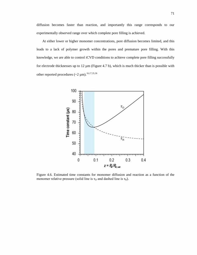
71
diffusion becomes faster than reaction, and importantly this range corresponds to our
experimentally observed range over which complete pore filling is achieved.
At either lower or higher monomer concentrations, pore diffusion becomes limited, and this
leads to a lack of polymer growth within the pores and premature pore filling. With this
knowledge, we are able to control iCVD conditions to achieve complete pore filling successfully
for electrode thicknesses up to 12 µm (Figure 4.7 b), which is much thicker than is possible with
other reported procedures (~2 µm).16,17,35,36
Figure 4.6. Estimated time constants for monomer diffusion and reaction as a function of the
monomerrelativepressure(solidlineisτD anddashedlineisτR).

72
Figure 4.7. Pore filling of TiO2 electrodes of different thicknesses of (a) 4 µm (scale bar=500
nm), and (b) 12 µm (scale bar=1 µm), the inset shows the bottom of the sample (scale bar=500
nm). By carefully controlling mass transport (gas and surface diffusion).
4.3.4 Pore filling quality
To provide a more quantitative measure of pore filling, cross sectional SEM was complemented
with TGA measurements to estimate the % pore filling, defined as the percent of the total pore
volume initially within the mesoporous TiO2 electrode (Vpore,L) which has been grown with
polymer by iCVD polymerization (Vpolymer,L), refer to Figure 4.8.
(4-10)
Toestimatethe%porefillingofthenominal12μmthickelectrode, first the porosity (ε) of the
initial, unfilled TiO2 electrode layer is derived from the N2 adsorption and desorption isotherms.
From the total volume of the adsorbate (~136 cm3/g STP), ε is estimated to be 0.43-0.45 Then,
cross sectional SEM was performed on the polymer filled TiO2 electrode to obtain an average
value of the thickness of the TiO2 electrode layer (L) and the top overcoating (δ)as12.7±0.1μm
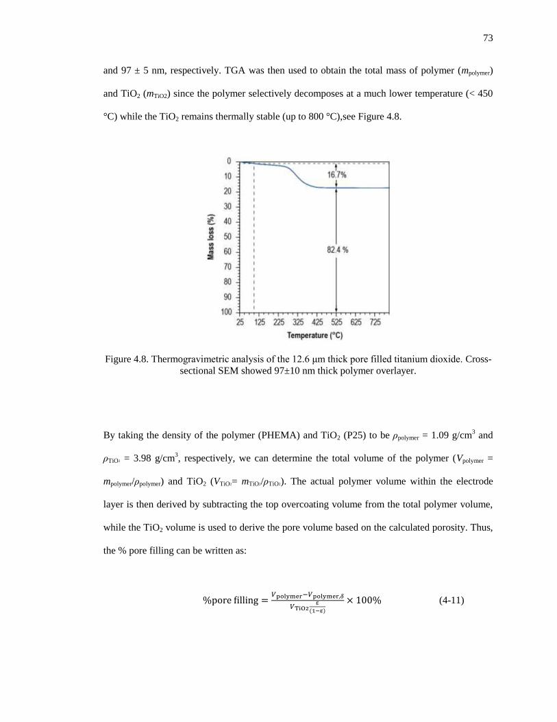
73
and 97 ± 5 nm, respectively. TGA was then used to obtain the total mass of polymer (mpolymer)
and TiO2 (mTiO2) since the polymer selectively decomposes at a much lower temperature (< 450
°C) while the TiO2 remains thermally stable (up to 800 °C),see Figure 4.8.
Figure 4.8. Thermogravimetricanalysisofthe12.6μmthickporefilledtitaniumdioxide. Cross-
sectional SEM showed 97±10 nm thick polymer overlayer.
By taking the density of the polymer (PHEMA) and TiO2 (P25) to be polymer = 1.09 g/cm3 and
TiO2 = 3.98 g/cm3, respectively, we can determine the total volume of the polymer (Vpolymer =
mpolymer/ polymer) and TiO2 (VTiO2= mTiO2/ TiO2). The actual polymer volume within the electrode
layer is then derived by subtracting the top overcoating volume from the total polymer volume,
while the TiO2 volume is used to derive the pore volume based on the calculated porosity. Thus,
the % pore filling can be written as:
(4-11)

74
Finally, by rewriting Equation 4-11 in terms of measured and literature values, the % pore filling
is calculated as:
(4-12)
Figure 4.9. The filled mesoporous of thickness L with δ polymer overlayer.
Thus, for the nominal 12 µm thick mesoporous TiO2 electrode pore filled with PHEMA polymer
electrolyte by iCVD, we estimate the % pore filling to be within the range of 92-100%. The
uncertainty is a result of the sensitivity range of the TGA and porosity measurements as well as
variability in the thickness and density values. Although the % pore filling can only be treated as
a rough estimate, the near 100% value indicates effective pore filling using the iCVD approach.
4.3.5 Polymer integrated DSSC performance
4.3.5.1 Effect of photosensitizer
Once proper conditions for pore filling were found, we applied iCVD and integrated PHEMA as
a polymer electrolyte in the dye sensitized TiO2 electrode. After incorporating the iodide-
triiodide redox couple in 50:50 propylene carbonate and γ-butyrolactone and assembling into a

75
complete quasi solid state DSSC, photocurrent-voltage measurements were made and compared
with a standard liquid electrolyte cell containing acetonitrile. As shown in Figure 4.10., although
the short circuit current density (Jsc) of the polymer electrolyte DSSC is reduced, the open circuit
voltage (Voc) is notably higher when compared with the acetonitrile liquid electrolyte cell. Now,
looking at cells of the same electrolyte across the two different dyes, the cells with dye 535 show
better performance than with dye 505. Dye 535 has a maximum light absorption that is red
shifted by about 50 nm when compared with dye 505.1 As a result, the incident photon to
electron conversion efficiency (IPCE) of the cell with dye 535 is superior to the one with dye
505. We therefore utilized dye 535 in the rest of this work.
Figure 4.10. Current-voltage characteristics of DSSCs fabricated with the polymer electrolyte
containing 50:50 vol% propylene carbonate and γ-butyrolactone (), and with the standard
acetonitrileliquidelectrolyte()incorporatingrutheniumdyes(a)535orN3,and(b)505.
4.3.5.2 Effect of electrolyte
To further understand the resulting Voc enhancement in the polymer electrolyte DSSC, we
compared the current-voltage characteristics of this cell with liquid cells containing the same

76
redox solvent rather than acetonitrile. As shown in Figure 4.11, when either a 50:50 % of
propylene carbonate and γ-butyrolactone or pure propylene carbonate was used to incorporate
the iodide-triiodide redox couple, we see that Jsc does not change significantly between the liquid
and polymer electrolyte cells using the same solvent as it does between the acetonitrile and
polymer electrolyte cells. In contrast, Voc is again consistently higher in both cases for the
polymer cell when compared with their liquid counterparts. This implies that since Jsc is not
affected the increase in Voc cannot have come from a difference in ion conduction as a result of
changing from a liquid to a quasi solid state polymer electrolyte. We further compared polymer
cells with complete fill and partial fill showing premature blockage. As shown Figure 4.12 the
partially filled polymer cells again show little change in Jsc while the increase in Voc is now much
smaller than if the electrode were completely filled.
The Voc for the sample with complete pore filling is much higher when compared with the
partially pore filled, which is higher than that with the liquid electrolyte. The Jsc however
remains in the same range. This demonstrates the need for complete pore filling to derive the
maximum benefit of the polymer electrolyte in enhancing DSSC performance as a result of the
largest gain in Voc.

77
Figure 4.11. Effect of redox solvent on the performance of DSSCs fabricated with the polymer
electrolyte()andthecorrespondingliquidelectrolyte()containing(a)50:50vol%propylene
carbonate and γ-butyrolactone, and (b) pure propylene carbonate. In each case, Voc is enhanced
while Jsc remains relatively unchanged in the polymer electrolyte cell.
Figure 4.12. Current-voltage characteristics of DSSCs containing 50:50 vol% propylene
carbonate and γ-butyrolactoneporefilledpolymerelectrolyte(),partiallyporefilledpolymer
electrolyte(),andliquidelectrolyte().

78
4.3.5.3 Effect of photoanode thickness
To further elucidate the effect of PHEMA pore filling, we investigated the changes in DSSC
performance with increasing TiO2 thickness and again made comparisons between polymer
electrolyte and acetonitrile liquid electrolyte cells, as detailed in Figure 4.13 Based on current-
voltage measurements, power conversion efficiency η of each cell has been derived from Jsc and
Voc as well as its fill factor FF, defined as the ratio of the actual maximum power to the
theoretical derivable power (i.e., Jsc×Voc). Knowing the power density of the illuminated
light(Wo), cell efficiency has been calculated as η=(FF×Jsc×Voc)/Wo.
As expected, the standard liquid cell shows a considerably smaller Voc with thicker
electrodes, which is typically attributed to an increase in recombination sites for the redox
couple (triiodide) to recapture dye injected electrons from the TiO2 as more surface area is
available.42,43
Similarly, the increase in surface area with thicker electrodes leads to higher Jsc in
the liquid cell with the greater amount of photosensitization. In contrast, for the completely pore
filled polymer electrolyte cell, Voc and Jsc appear to be less sensitive to electrode thickness
especially as electrode thickness increases above 4 µm. The smaller effect on Voc could be due to
passivation of the TiO2 surface when in contact with the iCVD polymer as has been observed
with small molecules.43
However, it is clearly evident that Voc is consistently much higher for the

79
Figure 4.13. Comparison between the performance of DSSCs fabricated with a quasi-solid state
PHEMA polymer electrolyte containing 50:50 vol% propylene carbonate and γ-butyrolactone
(), and with a standard liquid electrolyte containing acetonitrile () for different TiO2
thicknesses, showing (a) open circuit voltage Voc, (b) short circuit current Jsc, (c) fill factor FF,
and (d) power conversion efficiency η (error bar=1 SD). Polymer electrolyte DSSCs provide
similar efficiency as the liquid electrolyte cells with TiO2 electrode thicknesses that are nearly
three times thinner.
polymer cell compared to the liquid one at all electrode thicknesses we tested. There seems to be
a leveling off of Jsc which suggests some saturation effect, and could be a result of an increase in
diffusion resistance to ion conduction of the redox couple within the polymer matrix.
It is known that as the concentration of the iodide-triiodide redox species (using acetonitrile
as the redox solvent and liquid electrolyte) falls below some threshold, Jsc will plateau to a
limiting value with increasing light intensity.43
Likewise, in our case as shown in Figure 4.13, as

80
illuminated light intensity increases for the polymer electrolyte cell at constant electrode
thickness (~4 µm), Jsc becomes limiting at sufficiently low redox concentration. In contrast, for
the liquid electrolyte cell here, no plateau is observed for the range of redox concentrations
tested. The observed limiting behavior in the polymer cell can be attributed to the onset of
diffusion limited ion transport in the electrolyte due to a decrease in ion concentration gradient.43
Since the concentration gradient is influenced not only by the amount of redox species present
Figure 4.14. The effect of illuminated light intensity on short circuit current density of DSSCs
utilizing (a) liquid electrolyte, and (b) polymer electrolyte, each containing propylene carbonate
with different redox concentrations (in I2(M):LiI(M)) of 0.01:0.1 (∎), 0.08:0.8 (), and 0.2:2.0
() iodine and lithium iodide, respectively.
but also by the distance for ion transport, the diffusional limitation can be used to explain the
Jsc plateau observed in
Figure 4.14 for polymer cells when the TiO2 electrode thickness increases above 4 µm. Given
that the plateau is not observed for liquid electrolyte cells in all our cases, this suggests that ion
transport in these cells do not reach the threshold to become diffusion limited.

81
Since this behavior is only observed in the polymer electrolyte cell, the trends suggest
charge transport rather than charge generation becomes limiting, see Supporting Information for
more details. In Figure 4.13, although Jsc is lower, the significantly higher Voc together with a
relatively constant FF yield higher device efficiency for the polymer electrolyte cell compared
with the liquid acetonitrile cell at all the electrode thicknesses considered. In fact, the polymer
cell efficiencies remain fairly constant as a result of a lack of sensitivity of the device
parameters. As an important note, the difference in efficiencies observed between the polymer
and liquid electrolyte cells is solely due to the replacement of the liquid with the polymer, and
there has been no attempt to fully optimize cell performance. Significantly, the DSSC integrating
the iCVD PHEMA electrolyte can provide similar efficiency as the acetonitrile liquid electrolyte
DSSC using TiO2 electrodes that are a nearly factor of three thinner. Importantly, this implies
that there could be potential advantages when we consider a similar factor in reducing materials
usage, especially of the expensive dye, as well as the possibility of greater cell robustness,
particularly when thinking of applying the cell architecture on flexible substrates.
4.3.6 Electrochemical impedance spectroscopy
We therefore performed electrochemical impedance spectroscopy on the polymer and liquid
cells at their respective Voc to gain further insight. Figure 4.15 shows the Bode plots of the
polymer and liquid electrolyte DSSCs containing propylene carbonate, and illuminated under 1
sun corresponding to global AM 1.5 and 100 mW/cm2 irradiance. We observe a shift in the mid-
frequency peak towards lower frequency when the liquid electrolyte is replaced with the
polymer. This spectral peak frequency is a measure of the recombination time constant of the
electrons with the redox couple44
(triiodide) if we assume that charge recombination with the
oxidized dye molecules can be neglected due to fast reduction of the dye through the redox

82
couple.28
Thus, the shift to lower frequency suggests an increase in effective electron lifetime
from ~12 ms in the liquid cell to ~50 ms in the polymer electrolyte cell due to reduced
recombination with the electrolyte. We believe this decrease in charge recombination is the
cause for the substantially higher Voc. It is reasonable to expect that the contact of the quasi solid
polymer with the TiO2 electrode surface through complete pore filling can alter interfacial
properties. For example, charge transfer via surface trap states could be reduced by the polymer
Figure 4.15. Comparison between the Bode diagrams at their respective Voc of DSSCs fabricated
with the polymer electrolyte () and the corresponding liquid electrolyte () containing
propylene carbonate. The shift of the mid-frequency peak to lower frequency of the polymer
electrolyte cell indicates a decrease in charge recombination at the electrolyte-electrode
interface.
blocking active sites on the TiO2 surface.45
Also, it is possible that Li+ ions (from the redox
species) could coordinate with the polymer matrix thereby limiting lithium adsorption on the
TiO2 surface, which would result in band edge movement and consequently an increase in Voc of
the cell.46
83
4.4 Conclusions
We have successfully utilized iCVD to integrate a polymer electrolyte into the mesoporous TiO2
electrode of the DSSC. By carefully controlling diffusion transport and surface kinetics during
iCVD, complete pore filling can be obtained. The model prediction showed a good match with
the observed phenomena. This results in significant enhancement in cell properties. The
efficiency of the quasi solid state PHEMA electrolyte DSSC is higher when compared with their
liquid electrolyte counterparts. We attribute the observed increase in open circuit cell voltage to
the suppression of electron recombination at the electrolyte-electrode interface as a result of the
exceptional pore filling achieved by iCVD. iCVD promises to be a valuable synthesis and
processing pathway which as demonstrated here has the potential to overcome the major
technological constraint of using a liquid electrolyte in the DSSC.
4.5 References
1. EIA, Annual Energy Outlook with Projection to 2035, Released 2010.
2. J. B. Baxter, Journal of Vacuum Science & Technology A, 2012, 30, 020801-020819.
3. Y. Chiba, A. Islam, Y. Watanabe, R. Komiya, N. Koide and L. Y. Han, Japanese
Journal of Applied Physics, 2006, 45, L638-L640.
4. A. Yella, H.-W. Lee, H. N. Tsao, C. Yi, A. K. Chandiran, M. K. Nazeeruddin, E. W.-G.
Diau, C.-Y. Yeh, S. M. Zakeeruddin and M. Grätzel, Science, 2011, 334, 629-634.
5. M. D. McGehee, Science, 2011, 334, 607-608.
6. M. Ikegami, J. Suzuki, K. Teshima, M. Kawaraya and T. Miyasaka, Solar Energy
Materials and Solar Cells, 2009, 93, 836-839.

84
7. U. Bach, D. Lupo, P. Comte, J. E. Moser, F. Weissortel, .Salbeck,H.SpreitzerandM.
Grätzel, Nature, 1998, 395, 583-585.
8. . ruger,R.Plass,M.Grätzel andH. J. Matthieu, Applied Physics Letters 2002, 81,
367-369.
9. Q. B. Meng, K. Takahashi, X. T. Zhang, I. Sutanto, T. N. Rao, O. Sato, A. Fujishima, H.
Watanabe, T. Nakamori and M. Uragami, Langmuir, 2003, 19, 3572-3574.
10. D. Gebeyehu, C. J. Brabec and N. S. Sariciftci, Thin Solid Films, 2002, 403, 271.
11. Y. Saito, N. Fukuri, R. Senadeera, T. Kitamura, Y. Wada and S. Yanagida,
Electrochemical Communications, 2004, 6, 71-74.-274
12. F. Cao, G. Oskam and P. C. Searson, Journal of Physical Chemistry, 1995, 99, 17071-
17073.
13. R. Komiya, L. Y. Han, R. Yamanaka, A. Islam and T. Mitate, Journal of Photochemistry
and Photobiology A, 2004, 164, 123-127.
14. A. F. Nogueira, J. R. Durrant and M. A. De Paoli, Advanced Materials, 2001, 13, 826-
830.
15. J. H. Wu, Z. Lan, J. M. Lin, M. L. Huang, S. C. Hao, T. Sato and S. Yin, Advanced
Materials, 2007, 19, 4006-4011.
16. J. Wu, S. Hao, Z. Lan, J. Lin, M. Huang, Y. Huang, P. Li, S. Yin and T. Sato, Journal of
the American Chemical Society, 2008, 130, 11568-11569.
17. G. P. Bartholomew and A. J. Heeger, Advanced Functional Materials, 2005, 15, 677-
682.
18. B.O’Regan,F. enzmann,R.Muisand .Wienke,Chemistry of Materials, 2002, 14,
5023-5029.
19. .Schmidt-MendeandM.Grätzel, Thin Solid Films, 2006, 500, 296-301.
20. .H. um,P.Chen,M.GrätzelandM. K. Nazeeruddin, ChemSusChem, 2008, 1, 699-
707.
21. S. Nejati and K. K. S. Lau, Nano Letters, 2010, 11, 419-423.

85
22. S. Pavasupree, S. Ngamsinlapasathian, Y. Suzuki and S. Yoshikawa, Material Research
Bulletin, 2008, 43, 149-157.
23. J. B. Asbury, N. A. Anderson, E. Hao, X. Ai and T. Lian, Journal of Physical Chemistry
B, 2003, 107, 7376-7386.
24. J. Nelson and R. E. Chandler, Coordination Chemistry Reviews, 2004, 248, 1181-1194.
25. B.O’ReganandM.Grätzel, Nature, 1991, 353, 737-740.
26. A. N. M. Green, R. E. Chandler, S. A. Haque, J. Nelson and J. R. Durrant, Journal of
Physical Chemistry B, 2004, 109, 142-150.
27. A. J. Frank, N. Kopidakis and J. v. d. Lagemaat, Coordination Chemistry Reviews, 2004,
248, 1165-1179.
28. A.HagfeldtandM.Grätzel, Accounts of Chemical Research, 2000, 33, 269-277.
29. A. C. Fisher, L. M. Peter, E. A. Ponomarev, A. B. Walker and K. G. U. Wijayantha,
Journal of Physical Chemistry B, 2000, 104, 949-958.
30. H. Yang, M. Huang, J. Wu, Z. Lan, S. Hao and J. Lin, Materials Chemistry and Physics,
2008, 110, 38-42.
31. A. Kay, M. Nazeeruddin, I. Rodicio, R. Humpbry-Baker, E. Müller, P. Liska, N.
Vlachopoulos and M. Grätzel, Journal of the American Chemical Society, 1993, 115,
6382-6390.
32. S. S. Lowell, J.E.; Thomas M.A.; Thommes, M. , Characterization of Porous Solids and
Powders: Surface Area, Pore Size and Density, Springer, Dordrecht, Netherlands 2005.
33. G. L. Rumble, T.; Murakoshi, K., Electron transfer in nanomaterials, Proceedings of the
Electrochemical Society, 2004, 22, 126-136.
34. G. Ozaydin-Ince and K. K. Gleason, Chemical Vapor Deposition, 2010, 16, 100-105.
35. S. H. Baxamusa and K. K. Gleason, Chemical Vapor Deposition, 2008, 14, 313-318.
36. K. K. S. Lau and K. K. Gleason, Macromolecules, 2006, 39, 3695-3703.

86
37. J. G. Choi, D. D. Do and H. D. Do, Industrial & Engineering Chemistry Research, 2001,
40, 4005-4031.
38. R. Valiullin, P. Kortunov, J. Kärger and V. Timoshenko, Magnetic Resonance Imaging,
2005, 23, 209-213.
39. R. Valiullin, P. Kortunov, J. Karger and V. Timoshenko, Journal of Chemical Physics,
2004, 120, 11804-11814.
40. R. Valiullin, J. Karger and R. Glaser, Physical Chemistry Chemical Physics, 2009, 11,
2833-2853.
41. S. Beuermann and M. Buback, Progress in Polymer Science, 2002, 27, 191-254.
42. S. Ito, S. M. Zakeeruddin, R. Humphry-Baker, P. Liska, R. Charvet, P. Comte, M. K.
Nazeeruddin, P. Pechy, M. Takata, H. Miura, S. chida and M. Grätzel, Advanced
Materials, 2006, 18, 1202-1205.
43. S. . Huang, G. Schlichth rl, A. . Nozik, M. Grätzel and A. J. Frank, Journal of
Physical Chemistry B, 1997, 101, 2576-2582.
44. R. Kern, R. Sastrawan, J. Ferber, R. Stangl and J. Luther, Electrochimica Acta, 2002, 47,
4213-4225.
45. .Moser,S.Punchihewa,P.P. nfeltaandM.Grätzel, Langmuir, 1991, 7, 3012-3018.
46. G. Redmond and D. Fitzmaurice, Journal of Physical Chemistry, 1993, 97, 1426-1430

87
5 Integration of conducting polymers in supercapacitors
5.1 Introduction
With increased interest in more sustainable energy production and resources a challenging
question that remains to be answered is how to store the produced energy. Fossil fuels possess
very high energy densities that can be released by their burning. At the current moment there is
no alternative that matches their efficiency although their efficiency (Carnot efficiency) is not
phenomenal. Although the sun promises to be a clean energy resource, energy storage is
challenging given its intermittent availability. One possible answer to the energy storage
challenge is to store the energy in a similar fashion to fossil fuels, which is to utilize chemical
reactions and transformations of chemical bonds. This can be achieved through the use of redox-
active materials, which have the ability to be involved in electron transfer reactions.
Electrochemical storage is a way of storing generated power. Among different
electrochemical devices, batteries and capacitors are among the most studied systems and
currently for the huge portion of our needs for energy storage on a small scale we have relied on
batteries. Capacitors on the other hand when compared with batteries have much higher power
density but they suffer from significantly lower energy density. Comparing the electrochemical
capacitor and battery, it is worth pointing out the major differences that cause the observed
differences in their performance. In batteries, the electrochemical reaction of an ion with the
active electrode materials takes place within the bulk of the solid material and to reach the
charged state ions need to diffuse into the bulk solid. This is a slow process that makes its
charge-discharge far slower when compared with the electrochemical capacitor which store
charge only at the surface of the polarized electrodes in the form of an electrical double layer.
Nevertheless the charge being stored due to the screening of the electrical field of the electrode
within the solution is not significant in electrochemical capacitors as the double layer

88
capacitance dimension shrinks to the nm range.1 The fast charge-discharge of the
electrochemical capacitor when compared with a battery is the reason behind their higher power
density, however their total capacitance suffers from the larger dimension at which charge
storage must take place. Thus, there is a need to introduce new materials that have both high
power and energy densities. In the past twenty years, pesudocapacitors have been introduced that
incorporate battery-like redox reactions into electrochemical capacitors and there are hopes that
these material can act as an intermediate between batteries and capacitors or even outperform
both.1
An interesting aspect of conjugated polymers is their ability to be doped and therefore the
possibility to take part in redox reactions. The doping processes in conjugated polymers
correspond to oxidation in the case of p-doping or reduction in the case of n-doping. That means
the doping processes correspond to redox reactions in the polymer matrix. From an applications
point of view, it is important to know the phenomenological details of such redox reactions,
which potential range charging occurs and what is the maximum level of oxidation that can be
achieved before the material starts to degrade. Charge storage and transport in conducting
polymers were both of interest from the early stages of conducting polymer development.2 From
a practical point of view, a high charge storage capacity in these polymers is favorable for device
fabrication. Here, we explore the application of conducting polymers synthesized through oCVD
and integrated within nanostructured electrodes of supercapacitors.
5.2 Supercapacitors
Electrochemical capacitor is not a new field. It dates back to 1957 when Becker used a porous
carbon material to store charge in a double layer at the solid/electrolyte interface.3
Electrochemical capacitors however can rely on both an electrical double layer and

89
pseudocapacitance.1 Pseudocapacitance arises whenever there is a continuous charge that passes
faradaically with electrode voltage. In a sense pseudocapacitance is a phenomenon that take
place on the surface but has the nature of faradaic processes and is highly reversible. It passes
the charge through the double layer as in battery charging-discharging, but the capacitance arises
on account of special thermodynamic reasons between the extent of charge and the potential of
the electrode.1
Different materials have shown to possess high pseudocapacitance including some oxides
such as RuO2 , MnOx and conducting polymers.5,6
Among these, conducting polymers due to
their, low cost, flexibility, and ease of processing seems to be good a candidate. However
compared to oxides with cycle stability reported as high as 105 cycles,
7 conducting polymers still
need improvement. Another aspect of conducting polymers that has been reported lately is the
structural dependency of charge storage.8-11
It has been recently realized that the polymers when
spread into higher surface area by introducing nano- and mesostructured domains can actually
accumulate more charge.11
Here, we used oCVD as a powerful tool to synthesize high quality
polythiophene and integrated polymeric material within nanostructure electrode to investigate
the effect of nanostructure in polymer charge storage capacity.
5.3 Experimental
5.3.1 Polymer synthesis
To enable oxidative chemical vapor deposition, we have used an oCVD reactor system described
in detail elsewhere.12
Briefly, the reactor chamber was evacuated to base pressure (ca. 5 mtorr)
using a dry vacuum pump (Edwards Vacuum). Monomer, thiophene (97%, Sigma Aldrich), and
oxidant initiator, antimony pentachloride (99%,Across organic), were used as received and
metered independently from glass source vessels into the chamber using precision metering

90
valves (Swagelok). The initiator was heated up to 50 °C to achieve sufficient vapor pressure and
its temperature was kept constant using a temperature controller (Omega Engineering). The
monomer had sufficient vapor pressure at room temperature and was not heated. The chamber
pressure was measured with a pressure transducer (MKS Instruments) and automatically
maintained by using a downstream throttle valve connected to a pressure controller (MKS
Instruments). The substrate temperature was kept constant through backside cooling of the
reactor stage by using a recirculating chiller (Thermo Scientific Neslab).
In order to tune the oCVD polymerization reaction and synthesis chemistry at the surface,
the ratio of the reactant (monomer, initiator) partial pressure to its saturated vapor pressure at the
temperature of the substrate (i.e., Pr/Pr,sat) was carefully adjusted and controlled (see Discussion).
Thus, pressures ranging from 0.4-2 torr, and monomer and initiator flow rates of 0.5-5 and 0.1-
0.5 sccm (standard cm3/min), respectively, were studied. The substrate temperature was set at 30
°C. Polythiophene films were deposited on various substrates, including fluorine-doped tin oxide
glass (15/,HartfordGlass),siliconwafers(WRSMaterials),microscopeglassslides(Fisher
Scientific), and quartz glass (Chemglass) and within porous structure of TiO2 and anodized
aluminum oxide membrane (Anodisc, Whatman).
5.3.2 Polymer characterization
Fourier transform infrared spectra (FTIR) were acquired on a Thermo Nicolet 6700 spectrometer
in normal transmission mode using an MCT/A detector at a resolution of 4 cm-1
averaged over
64 scans. UV-vis spectra of deposited films on quartz glass were acquired between 280-800 nm
with 1 nm resolution using a Shimadzu UV-1700 spectrophotometer. X-ray photoelectron
spectroscopy (XPS) was performed on a Physical Electronics PHI 5000 VersaProbe with a
scanning monochromatic source from an Al anode and with dual beam charge neutralization.
91
Survey XPS spectra were acquired at 100 W with pass energy of 117 eV over the range of 0-
1100 eV with 1 eV resolution and 100 ms dwell time, and averaged over 2 scans. High
resolution XPS spectra of C1s, O1s, Sb3d, Cl2p and S2p core electrons were acquired in high
power mode of 100 W with a pass energy of 11.5 eV for C1s, Cl2p and S2p and 23.5 eV for O1s
and Sb3d using different acquisition times chosen based on the observed intensity of the
elements from the surveys. Raman spectra were collected on a Renishaw RM1000
microspectrometer using an Ar ion laser 488 nm with ~1 µm lateral spot size and 11 mW total
power and He-Ne laser 633nm with ~1 µm lateral spot size and 10 mW total power. Cyclic
voltammograms were recorded in a three electrode setup under a nitrogen blanket with a Gamry
Reference 600 potentiostat. The polythiophene samples deposited on FTO glass served as the
working electrode while a 2.5x2.5 cm platinum gauze (Princeton Applied Research) was used as
the counter electrode. The silver reference electrode (Princeton Applied Research) was filled
with 0.1 M silver nitrate (99.9999%, Sigma Aldrich) and 0.1 M tetraethylammonium perchlorate
(electrochemical grade, Sigma Aldrich) in acetonitrile (ACS grade, Sigma Aldrich). A
supporting electrolyte of 0.1 M tetrabutylammonium hexafluorophosphate (electrochemical
grade, Fluka) in acetonitrile was bubbled for 1 h with nitrogen prior to use. The potential was
swept between -0.4 and 1.2 V vs. Ag/AgNO3 with a sweep rate of 80 mV/s. The charge storage
capability of the samples deposited on planar FTO glass, and within mesoporous titanium
dioxide and activated carbon electrodes were tested by performing cyclic voltammetry in a three
electrode setup using organic salts e.g. tetraethylammonium tetrafluoroborate in acetonitrile as
the electrolyte, an Ag/AgCl reference electrode. The reference was calibrated using Fe+/Fe in
acetonitrile using a glassy carbon electrode as the working electrode and a platinum mesh as the
counter electrode. Polythiophene film conductivity was estimated through measuring sheet
resistivity using an Alessi four point probe connected to a Keithley 2400 source meter.

92
5.3.3 TiO2 electrode fabrication
The titanium dioxide colloidal paste consisting of TiO2 nanoparticles P25 (Envonik) was
prepared using a published procedure.13
The prepared paste was spin coated at 800 rpm onto
fluorinedopedtinoxideconductiveglass(HartfordGlass,15Ω/) to obtain a film of the paste
between 4 µm in thickness. To create the mesoporous structure, the spin coated TiO2 paste was
heated up to 500°C and annealed for 30 min.
5.3.4 Activated carbon electrode fabrication
Activated carbon electrodes were fabricated in two different ways and tested on two different
current collectors in two different configurations. Activated carbon particle YP-50 (Kurary inc)
with 1500-1700 cm2/g and average particle size in between 5-20 µm were used as received. A
suspension of activated carbon in ethanol % 0.5 w/w was made and mixed for 2 h at room
temperature. 50 µl of this solution were pipetted in between two piece tap placed parallel on the
FTO and treated stainless steel and allowed to dry in the oven for 24 h at 100 °C and were kept
in the oven at room temperature till they were used for electrochemical measurements.
The activated carbon mat was fabricated according to published protocol14
using YP-50 and
%5.0 binder (% 60 aqueous solution of PTFE) to obtain 100 µm thick electrodes. Briefly the
particles were mixed with the ethanol and then binder was added drop-wise while stirring the
mixture. The whole mixture was heated for 2 h at 60 °C and semi-dry pastes were spread on a
piece of glass and kneaded till a gum-quality paste was obtained. The mat was dried in the oven
at 120 °C for 24 h and stored under an inert atmosphere till they were further used.

93
5.3.5 Current collectors
As for FTO, the glass slides were sonicated in dilute detergent solution (Citranox) and
thoroughly rinsed in deionized water and sonicated again in ethanol for 10 min followed by
heating to 400 °C to remove any contamination from the surface caused by solvent adsorption.
They were then stored in an inert environment until they were further used.
For the stainless steel plate, 0.5 mm thick stainless steel plates (McMaster Carr) were cut to
size. The plates were mechanically roughened using 400 grit SiC paper and then washed and
rinsed in DI water and sonicated in ethanol for 10 min. The surface of the current collectors were
etched in a solution of 1 M NaOH (Aldrich) for 10 min at room temperature and then rinsed with
DI water and immediately dipped into a 1 M HCl ( Aldrich) at 80 ºC for 10 min. The current
collectors were rinsed with water and dried in vacuum oven at 80 ºC for 15 min and kept under
vacuum until further use.
For the Swagelok setup the electrode set up was fabricated as described elsewhere.15
Two
stainless steel rods (3/8”,McMaster Carr) were used as the electrodes and their surfaces were
roughened with 40 grit SiC and then rinsed thoroughly with water and sonicated in ethanol for
20 min. The cleaned electrodes were dried in vacuum oven for 20 min at 80 °C and then were
transferred to a sputter coater to be coated with 5 nm of Pt coating.
5.3.6 oCVD polythiophene integration
As we have shown, polymer integration within nanostructured electrodes can be obtained by
carefully tuning the CVD parameters to be under a reaction-limited regime.16
The effect of
various oCVD parameters was studied first using a well-defined pore geometry of the AAO
membrane to determine the conditions at which conformal polythiophene could be achieved on
the inner walls of the pores. Pressure was varied to obtain a range at which the inner wall is

94
coated without premature pore blockage. So at 30 °C stage temperature, and 0.5, 5 and 2 sccm of
initiator, monomer and N2, respectively, we have changed pressure from 200 mtorr to 2 torr and
obtained control over coating inside the structure as thick as 40 nm before the pores were
blocked at the top. We then adjusted each reactant flow rate at a time to find the reaction-
limiting conditions. Ar was also used instead of nitrogen to eliminate any possible reaction of
nitrogen during deposition. This approach was repeated for the conformal deposition on
mesoporous TiO2 and activated carbon. The proper oCVD conditions for conformal coating
were different depending on the nature of the pores in each substrate.
5.3.7 Polymer weight measurement
Weight measurements for the polymer on planar substrates were done on a precision lab scale.
For very thin films (< 100 nm), due to the lack of sensitivity of the scale, thickness was instead
measured by cross-sectional SEM and related to weight based on a thickness-weight calibration
made with thicker films. For the polymer deposited within the nanaostructure of TiO2,
thermogravimetric analysis (TGA) was performed to estimate the mass of polymer. For the
polymer within the activated carbon, the mass was estimated from added mass to the support
using the lab scale.
5.4 Results and discussion
The oCVD synthesized polythiophene were deposited on different substrates. The films adhered
well to the underlying substrates and none of the common solvents we tested, including
tetrahydrofuran, chloroform, methanol, and methyl formamide, were able to dissolve the films.
Electrical conductivity reached values as high as 50-70 S/cm.

95
5.4.1 Vibrational spectroscopy
Figure 5.1 shows the FTIR spectrum of the as-deposited polythiophene. The strong vibration
band in between 1100 and 1500 cm-1
can be assigned to the doping induced vibrations of
polythiophene.17,18
The peaks observable at 790 and 690 cm-1
are characteristic of C–H out-of-
plane bending of the thiophene ring.19
The C–H stretches located above 3000 cm-1
also indicate
that the aromatic thiophene ring is preserved. Comparing this FTIR spectrum with the one
obtained for PTh deposited using VOCl3 as the oxidant, the first striking difference is the
absence of any oxidant residue peak at 900 cm-1
and between 1600-1700 cm-1
. This could
suggest less defects in the film as there is no peak associated with the oxidant residue in the film.
Figure 5.1. FTIR spectrum of an as-deposited doped film on silicon.

96
Since undoped polythiophene films exhibits very strong visible absorption bands related to
the π-π* electronic transition, whose maximum is located between 470-520 nm, 488 nm
excitation allowed these peaks to be enhanced and therefore indicative of the native polymer. In
addition, Raman spectra were acquired using 633 nm laser excitation to reduce the resonance
enhancement of the native state so that the effect of doping can be more clearly observed, see
Figure 5.2. The strong bands in between 1000-1300 cm-1
are indicative of highly doped polymer
when compared with the Raman spectrum of a washed, dedoped polymer. These results are in
agreement with previous reports20
on the doped polythiophene excited with the 633 nm beam
and suggest that the oCVD deposition of polythiophene using SbCl5 oxidant generated a highly
doped state.
To investigate the effect of oCVD synthesis parameters on polymer quality, the oxidant
concentration was adjusted by changing its flow rate from 0.1 to 0.5 sccm while keeping other
conditions constant (total pressure (P) =800 mtorr, monomer flow rate FM = 2 sccm, stage
temperature (Ts) = 30 °C). The Raman spectra of the polythiophene deposited at three different
condition that resulted in different conductivity ranging from 10 to 50 S/cm are shown in Figure
5.3. As seen, the region of interest that include the intra C=C vibration corresponding to the
quinoid structure shifts from 1450 to 1420 cm-1
as the conductivity increased. The film deposited
at 0.3 sccm of oxidant seems to have the maximum conductivity and as the oxidant
concentration is increased further the conductivity is reduced as shown by the shift of the
quinoid band to higher wavenumbers.

97
Figure 5.2. Raman spectra of PTh deposited on silicon, excited using (a) 488, and (b) 633 nm
laser beams.
Figure 5.3. Raman spectra of polythiophene deposited at different oCVD condition. The shift in
quinod peak to a lower wavenumber is concomitant with an increase in film electrical
conductivity.

98
5.4.2 UV-vis spectroscopy
UV-vis spectroscopy also confirms that the polythiophene films deposited using the new oxidant
has better structural properties as evidenced by the longer conjugation length that is indicated by
the red shift in the maximum absorption peak (max) to 515 nm compared to 480 nm for the film
deposited using the VOCl3 oxidant. Once again, by changing oCVD synthesis conditions film
properties can be tuned. Figure 5.4 shows the UV-vis spectrum of the deposited polymer on
quartz glass and the shift in absorption maximum as a result of changing the oxidant
concentration in the gas feed
Figure 5.4. UV-vis spectrum of an as-deposited film after dedoping the film to its undoped form
(by exposure to 2.0 M methylamine in methanol for 2 min followed by washing with neat
methanol). Inset shows the control over absorption spectrum by changing oCVD parameters, the
increase in conjugation length obtained by reducing the oxidant concentration.

99
5.4.3 Cyclic voltammetry of the deposited film on FTO
Figure 5.5 shows the cyclic voltammogram of an as-deposited polythiophene film measured in
an electrolyte of 0.5 M tetraethylammonium tetrafluoroborate (TEABF4) in acetonitrile. The p-
doping (oxidation) and dedoping (reduction) peaks are clearly observed at 0.8 and 0.25 V vs.
Ag/AgCl, respectively, and are accompanied by a color change from red in the undoped state to
deep blue in the doped form. The locations of these peaks match reported values of p-doping and
dedoping peaks for unsubstituted polythiophene.21
Figure 5.5. Cyclic voltammogram of an as-deposited film on FTO glass.
5.4.4 Polymer integration within nanostructures
Chemical vapor deposition is well-known to produce conformal coatings on topographically
complex substrates. Even with porous structures where the aspect ratio (length-to-diameter) of

100
the pores can exceed 1000:1 and pore sizes are on the nanometer scale, CVD is able to achieve
uniform and conformal coating on the pore walls,22
and if so desired, the pore spaces can even be
entirely filled.16
Here, we demonstrate a unique way to integrate unsubstituted polythiophene
within porous nanostructures with exceptional control over film thickness and coating
conformality by simple adjusting of oCVD synthesis parameters. We have chosen to deposit
within anodized aluminum oxide (AAO) membranes having well-defined pore geometries in
order to investigate the oCVD parameter space that leads to effective polymer integration. By
reducing total pressure and oxidant concentration so as to be in the reaction-limited regime that
favors mass transport inside the pores, we obtained conformal growth of the polymer within
porous nanostructures with average deposition rates as low as 0.5 nm/min (deposition rate was
estimated by taking the ratio of SEM-measured cross sectional film thickness and film
deposition time).
Figure 5.6 shows 57 µm thick AAO membranes with a nominal pore diameter of 200 nm,
comparing the white uncoated membrane (Figure 5.6a) to the polythiophene coated one which in
the as-deposited doped form has a dark grayish blue color (Figure 5.6b), and the polythiophene
coated disc after dedoping to yield the orange-red undoped state (Figure 5.6c). Cross-sectional
scanning electron microscopy (SEM) images show that the vertically aligned pore channels of
the AAO membrane (Figure 5.6d) have been conformally coated with polythiophene, in this case
with a film thickness of ~30 nm (Figure 5.6e). This uniform coating is observed throughout the
entire thickness of the AAO membrane and demonstrates oCVD's ability to create conformal
films along pore walls inside porous nanostructures by manipulating the rate of polymerization
at the surface relative to mass transport dynamics. It should be noted that with faster reaction
rates at higher oxidant flow rate, preferential deposition on the outer membrane surface rather
than inside the pores led to non-conformal coating and eventually pore blockage (not shown).

101
Figure 5.6. Conformal coating of polythiophene within porous nanostructures using oCVD. (a)
Uncoated anodized aluminum oxide (AAO) membrane, 57 µm thick and 200 nm pore diameter.
(b) Polythiophene coated AAO in the as-deposited doped state of the polymer. (c)
Polythiophene coated AAO in the undoped state of the polymer after dedoping. (d) Cross-
sectional SEM of an AAO membrane showing the porous channels (darker shade). (e) Cross-
sectional SEM of a polythiophene coated AAO membrane showing conformal and uniform. The
conditions used for filling AAO without mass transfer limitations up to 40 nm thick film on the
inner wall was as follow: 30 °C stage temperature, and 0.1, 2 and 2 sccm of initiator, monomer
and N2, and 800 mtorr total pressure.
We have applied our knowledge of oCVD to enable in-situ polymerization and conformal
coating of PTh within the nanostructure to mesoporous TiO2 supported on TO glass. As seen in
Figure 5.7, again by adjusting oCVD parameters we were able to deposit polymer within the
nanostructure in a conformal fashion. Since the pore structure was more tortuous and the aspect
ratio was even higher when compared with the AAO disk, we have increased FM from 2 to 5
sccm while reducing the total pressure to 500 mtorr as this allowed the rate of reaction to be
controlled within the TiO2 pores more effectively.

102
Figure 5.7. Polythiophene integrated TiO2 electrodes. (a) Undoped PTh (by exposure to 2.0 M
methylamine in methanol for 2 min followed by washing with neat methanol). (b) Cross-
sectional SEM of the mesoporous electrode with conformal PTh coating (scale bar is 200 nm).
5.4.5 Effect of nanostructure on charge storage
With the ability to create conformal coatings inside porous nanostructures, we turned our focus
to study the effect of a porous nanostructure on the electrochemical behavior of polythiophene
films. Here, oCVD was used to deposit polythiophene films on planar FTO substrates as well as
inside 4 µm mesoporous TiO2 layers supported on FTO substrates. The TiO2 layers consisted of
a network of 25 nm TiO2 interconnected nanoparticles spin coated from a suspension onto FTO
glass and annealed at 450 °C to remove the solvent, resulting in a mesoporous network structure.
Conformal coating inside mesoporous layers as thick as 4 µm was obtained at a slow deposition
rate of 1 nm/min (based on estimating an average film thickness by knowing the mass of
deposited polymer, the total available substrate surface area, and assuming a polymer density16
of 1.35 g/cm3). Before performing any electrochemical tests, the samples were soaked in
tetrahydrofuran (THF) for 3 h and dried in a vacuum oven for 8 h to remove THF completely.
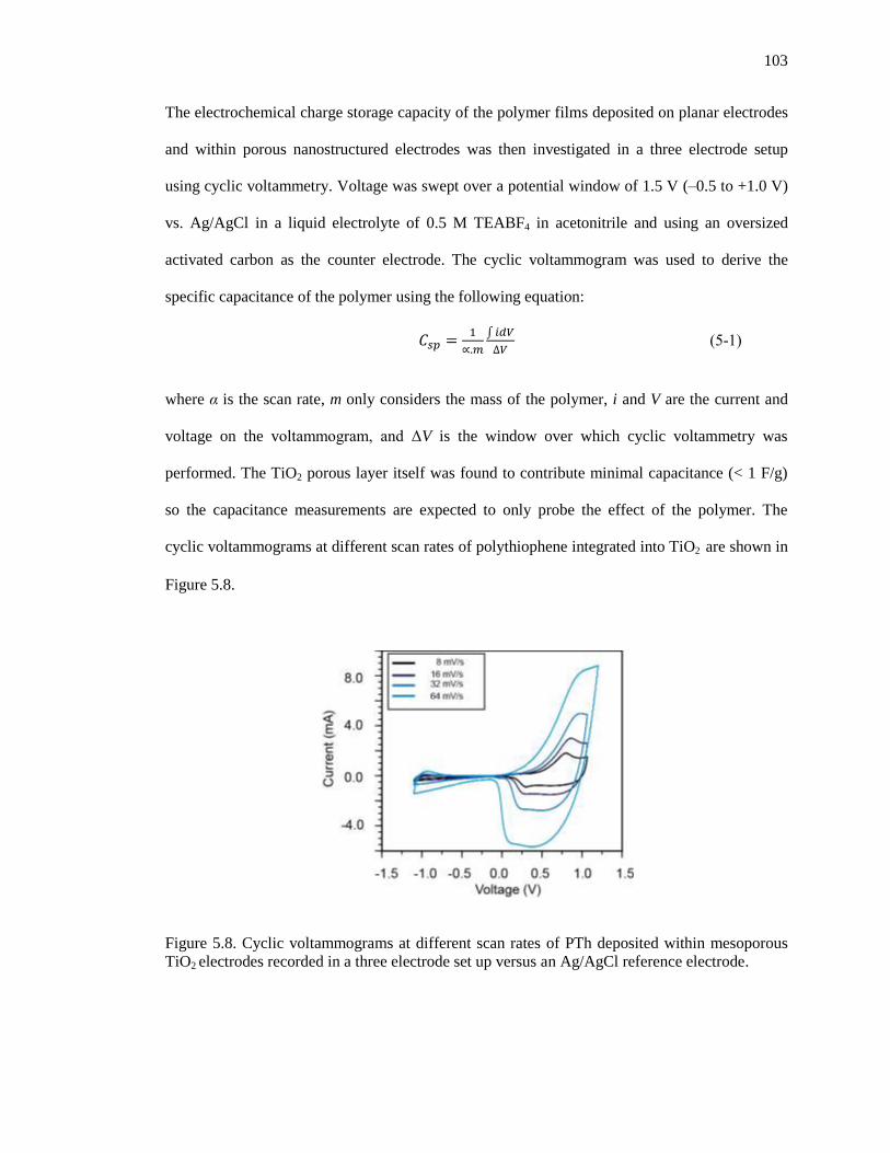
103
The electrochemical charge storage capacity of the polymer films deposited on planar electrodes
and within porous nanostructured electrodes was then investigated in a three electrode setup
using cyclic voltammetry. Voltage was swept over a potential window of 1.5 V (–0.5 to +1.0 V)
vs. Ag/AgCl in a liquid electrolyte of 0.5 M TEABF4 in acetonitrile and using an oversized
activated carbon as the counter electrode. The cyclic voltammogram was used to derive the
specific capacitance of the polymer using the following equation:
(5-1)
where α is the scan rate, m only considers the mass of the polymer, i and V are the current and
voltage on the voltammogram, and ΔV is the window over which cyclic voltammetry was
performed. The TiO2 porous layer itself was found to contribute minimal capacitance (< 1 F/g)
so the capacitance measurements are expected to only probe the effect of the polymer. The
cyclic voltammograms at different scan rates of polythiophene integrated into TiO2 are shown in
Figure 5.8.
Figure 5.8. Cyclic voltammograms at different scan rates of PTh deposited within mesoporous
TiO2 electrodes recorded in a three electrode set up versus an Ag/AgCl reference electrode.

104
Using the cyclic voltammograms we estimated the specific capacitance of the polymer knowing
the mass of the sample deposited on the electrodes. Figure 5.9a gives the specific capacitance
(per mass of the polymer) for polythiophene thin films deposited on planar substrates and inside
mesoporous TiO2 nanostructures. Clearly, there is a dependence of the specific capacitance on
polymer thickness both on the planar substrate (250 and 800 nm) and within the nanostructure (4
and 6 nm). Film thickness of polythiophene on the flat substrates was measured directly through
cross-sectional SEM while that inside the nanostructures was estimated by measuring the mass
gain due to the polymer after oCVD using thermogravimetric analysis (TGA) and relating it to
polythiophene density (1.2 g/cm3)
23 and the nanostructure specific surface area (55 m
2 /g,).
16 For
polythiophene deposited on planar substrates, the specific capacitance of thin films (down to 50
nm as the minimum film thickness practically possible for electrochemical measurements) over
the 1.5 V window was found to be 150 F/g and for thicker samples (> 450 nm) this value was
reduced to 75 F/g. To understand this difference, the anodic peak current taken from the cyclic
voltammogram was traced as a function of scan rate, see Figure 3b. For a planar thin film (250
nm), the linear response is characteristic of a reaction limited behavior in the redox process. In
contrast for a thick film (800 nm), the deviation from a linear response indicates that ion
diffusion and penetration inside the polymer becomes limiting. This is confirmed by the linear
relationship obtained by plotting the peak current with the square root of the scan rate (not
shown) predicted for the ion diffusion limited case, and which allows an estimate of the BF4– ion
diffusion coefficient of 8.9x10⁻⁹
m2/s to be obtained.
24 This value is in the range of diffusion
coefficient values reported for thiophene polymers in planar geometry.25
The difference in
specific capacitance between thin and thick polythiophene films is also seen for the case of the
polymer deposited within the mesoporous TiO2 nanostructures. As the polymer thickness
increased from 4 to 6 nm, the latter being close to the limit at which the pores become filled, the

105
specific capacitance was significantly reduced from 275 to 75 F/g, see Figure 5.9a. By plotting
the anodic peak current as a function of scan rate, as seen in Figure 5.9c, again the thicker
coating this time within the nanostructure shows that the redox process is highly diffusion
limited. Plotting the current with the square root of the scan rate yields a linear behavior for the
ion diffusion limited process, leading to a diffusion coefficient for BF4– ions to be 8.2x10
-8 m
2/s,
which is an order higher than that for the dense, thick planar polythiophene film but is
comparable to that reported for the diffusion of ions in a liquid electrolyte within nanoporous
electrodes.26
This suggests that diffusion in this case is limited by ion diffusion in the liquid and
not in the polymer, presumably due to the much narrower pore channels with the thicker
polymer coating inside the porous nanostructure.
What is more important with the results in Figure 5.9a is the significant enhancement in
specific capacitance when a thin polythiophene film is inside the mesoporous TiO2 layer
compared to a thin film on a planar substrate, where in both cases ion diffusion is not limiting. If
the thin polythiophene film inside the nanostructure were solely dictated by reaction controlled
redox processes, then the expected specific capacitance (per mass of polymer) should be similar
to that of the thin planar film. However, the measured capacitance for the film inside the porous
nanostructure is almost 1.6 times higher. The data suggests that the three-dimensional
nanostructured pore surface adds a significant component to the electrochemical behavior of
polythiophene that is not available on a two-dimensional planar surface. There are reports to
indicate that a nanoconfinement effect can significantly increase the electrical double layer
capacitance (EDLC) in nanoporous electrodes. This has been attributed to enhanced collision
frequency of ions with the pore walls as ions diffuse within a porous media (analogous to gas
phase Knudsen transport) as well as enhanced charge screening with the electric field
distribution inside the nanoporous structure.27
This increase in double layer capacitance due to
106
nanoconfinement has been shown to be a strong function of roughness (defined as the ratio of
actual to geometric surface area) and ion concentration in the bulk.28
However, for our case, the
enhanced charge capacity should come from Faradaic reactions of the polythiophene rather than
an electrical double layer since the bare TiO2 nanostructure had negligible measurable
capacitance. There is the possibility that the polythiophene might have a double layer
capacitance component that could lead to the nanoconfinement enhanced capacity as observed in
other double layer nanoporous structures since we see a flat rectangular portion in the cyclic
voltammograms (not shown) that suggest some double layer contribution (see below). It is also
possible that the faradaic processes in polythiophene could be augmented in a nanoconfined
polymer. The increase in ion collision frequency, the greater local ion concentration and the
changes in electric field distribution within the pores might help the ions to interact more
effectively with the polymer chains. The thinness and curvature of the polymer film might also
open additional sites for ion incorporation. These factors could lead to a greater amount of
charge being transferred during doping and dedoping. It is also possible that an increase in
faradaic current could arise from more stable oxidation of the polymer. In the bulk, further
oxidation can be achieved at higher electrode potentials,29
however in the case of unsubstituted
polythiophene this easily leads to over-oxidation in the presence of presence of nucleophillic in
the media that result in polymer degradation.30
However, with the polymer confined in the
nanopores, more oxidation could potentially be achieved without irreversible chemical
degradation since the pores might prevent these solvent nucleophiles from interacting with the
polymer.31,32,27
Although the reasons for enhanced capacity is not entirely understood, the effect
of a porous nanostructure on enhancing the specific capacitance of ultrathin polythiophene is
clearly observed.

107
Figure 5.9. Effect of polymer thickness and 3D nanostructure on the specific capacitance of
oCVD polythiophene. (a) SEM images (scale bar is 200 nm) and specific capacitance values of
thin (250 nm) and thick (800 nm) films on planar FTO electrodes, and of thin (4 nm) and thick
(6 nm) films inside mesoporous electrodes of TiO2; specific capacitance is based on per mass of
polymer and reported with 2 standard deviations. The current density of the anodic peak (doping
peak) as a function of scan rate for different thickness of films on (b) planar substrates and (c)
within mesoporous nanostructures.
108
5.4.6 Polymer integrated supercapacitors
Given the ability to significantly enhance charge storage with ultrathin oCVD polythiophene
within porous TiO2 nanostructures, we investigated further by using oCVD to integrate
polythiophene thin films within the nanostructure of activated carbon electrodes to create
supercapacitors. The activated carbon mat with 100 µm thick electrodes was cut into 1 cm2 size
for oCVD coating and electrochemical characterization was performed in a two electrode set up.
Unsubstituted polythiophene was then conformally coated within the porous activated carbon by
oCVD at various deposition times using a constant set of oCVD deposition conditions (1 Torr
pressure, 0.3 sccm oxidant flow rate, 2.5 sccm monomer flow rate, and 30 °C substrate
temperature) to obtain electrodes with different mass loadings of the polymer within the matrix.
Figure 5.10 show the top-down SEM images of the activated carbon particles in the fabricated
electrodes before and after oCVD with several mass loadings of polymer to activated carbon
(1:1, 1.5:1, and 2.7:1). As seen in Figure 5.10a, uncoated activated carbon particles have a very
rough surface consisting of microscale topologies and mesopores. With an increasing amount of
polythiophene as in Figure 5.10b and c, the surface morphology becomes noticeably smoother,
and eventually at high enough loading of the polymer as in Figure 5.10d the coating is sufficient
to cover the microscale features and fill in many of the pores.
The electrochemical performance of the fabricated electrodes after polythiophene dedoping
and THF washing and dried, were tested in a symmetric two electrode Swagelok cell15 using 1
M TEABF4 in acetonitrile as the electrolyte. A voltage range of –2 to 2 V was found to be an
appropriate window over which the fabricated electrodes were stable (this was based on separate
cyclic voltammetry measurements made beforehand in a three electrode setup where the
electrodes were used in a symmetric configuration and the voltage on the electrode was probed
independently vs. an Ag/AgCl electrode).33
Specific capacitance of the assembled Swagelok

109
cells was derived from cyclic voltammetry and using Equation 5-1, the only difference being
that the total mass of the electrode (including the polymer, activated carbon and binder) was
used in the calculation. As shown in Figure 5.10e, specific capacitance values of oCVD
polythiophene coated activated carbon pseudocapacitors are highly dependent on the mass
loading of polymer. In particular, at a polymer-to-activated carbon mass ratio of ~1.5, specific
capacitance reaches a maximum, a value ~50% higher than that for bare activated carbon (145
vs. 92 F/g). More significantly, this capacitance translates to over a 250% increase in volumetric
capacitance since the volume contribution of the ultrathin polymer coating is negligible (120 vs.
47 F/cm3). Figure 5.10f shows cyclic voltammetry sweeps of the polythiophene coated activated
carbon at the 1.5:1 mass ratio over a 4.0 V window at different scan rates. The dependency of
the peak current value upon the scan rate is not entirely linear but there is no sign of diffusion
limitations up to 100 mV/s. The pseudocapacitor is shown to be stable up to the 5000 cycles
tested with a small 5% capacitance drop during the first 100 cycles, see Figure 5.10g.
Looking back at each cyclic voltammogram in Figure 5.10f, we observe that the signal has
both characteristics of a pure electrical double layer capacitor (EDLC) and faradaic processes
associated with a pseudocapacitor. The flat portion of the curves around 0 V is characteristic of
the rectangular plot typically obtained with an EDLC such as activated carbon while the peaks
noticeable towards either edge of the voltage window relate to the redox reactions of a
pseudocapacitor like polythiophene. This suggests that the ultrathin polythiophene coating did
not completely block access to pores so that a considerable portion of the activated carbon
surface is still available for ions to dock at the surface and contribute to charge storage in
electrical double layers. This area could be mainly from the micropores that are inaccessible to
oCVD for conformal polymer coating and therefore activated carbon remains accessible to ions.
However, when the polymer coating becomes too thick, these pores no longer become accessible

110
and further; the surface features in activated carbon become more rounded and ill-defined. This
could lead to lower capacitance due to pore blockage, less surface area and even the onset of
diffusion limitations. This could explain the behavior observed in Figure 5.10e, in which the
maximum capacitance observed could be understood as an initial increase in the contribution
from pseudocapacitance with having more redox active polymer to an eventual decrease in
capacitance due to a drop in surface area and pore blocking with thicker polymer coatings.
Figure 5.10. Electrochemical behavior of oCVD polythiophene coated activated carbon. SEM
images of activated carbon electrodes (a) without coating, and coated with polythiophene at
polymer-to-activated carbon mass ratios of (b) 1:1, (c) 1.5:1, and (d) 2.7:1 (insets show a
magnified region of the surface morphology of each sample; scale bar is 1 µm and 50 nm for the
inset). (e) Specific capacitance values based on per total mass of electrode for different polymer
mass loadings. Measurements were made at 100 mV/s for five different samples at each loading
with the error bars representing two standard deviations. (f) Cyclic voltammograms of the 1.5:1
mass ratio pesudocapacitor recorded at different scan rates between –2 and 2 V. (g) Capacitance
of the same sample measured up to 5000 cycles (at 100 mV/s ).

111
5.5 Conclusions
We have demonstrated oCVD's unique ability to synthesize unsubstituted polythiophene based
on the direct vapor-to-solid oxidative polymerization of thiophene monomer using antimony
pentachloride oxidant. Ultrathin polythiophene films have been successfully integrated within
high aspect ratio porous nanostructures of AAO, TiO2 and activated carbon by operating oCVD
under slow kinetics that favor reactant mass transport. Significantly, ultrathin conformal
polythiophene coatings that preserve the high surface area of the porous nanostructures showed
enhanced capacitance 1.6 times over that of planar films that could be attributed to
nanoconfinement effects not available in open planar geometries. As a result, type I symmetric
pseudocapacitors consisting of polythiophene coated activated carbon electrodes displayed
significantly greater energy storage capacity compared to bare activated carbon, with an increase
of 50% and 250% in specific and volumetric capacitance, respectively, at an optimal polymer-to-
activated carbon mass ratio of 1.5:1. Capacitance was stable up to the 5000 cycles tested with a
small decrease of 5% within the first 100 cycles. The capacitance enhancement could be
attributed to the preservation of nanostructure surface area and accessible pore space that is
afforded by ultrathin films. oCVD promises to be a valuable synthesis and processing pathway
for making conductive polymers and creating enhanced energy storage solutions that takes
advantage of nanostructured device architectures.
5.6 References
1. B. E. Conway, Electrochemical Supercapacitors: Scientific Fundamentals and
Technological Applications, Plenum, New York, 1999.
2 M. Nowak, D. Spiegel, S. Hotta, A. Heeger and P. Pincus, Macromolecules, 1989, 22,
2917-2926.
3. H. I. Becker, United States patent, US 2800616, 1957.

112
4. D. Galizzioli, F. Tantardini and S. Trasatti, Journal of Applied Electrochemistry, 1974,
4, 57-67.
5. J. Zheng, P. Cygan and T. Jow, Journal of the Electrochemical Society, 1995, 142,
2699-2703.
6. A. Laforgue, P. Simon, C. Sarrazin and J.-F. Fauvarque, Journal of Power Sources,
1999, 80, 142-148.
7. T. Jow and J. Zheng, Journal of the Electrochemical Society, 1998, 145, 49-55.
8. H. Wang, Q. Hao, X. Yang, L. Lu and X. Wang, Nanoscale, 2010, 2, 2164-2170.
9. J. Xu, K. Wang, S.-Z. Zu, B.-H. Han and Z. Wei, ACS Nano, 2010, 4, 5019-5026.
10. K. Zhang, L. L. Zhang, X. S. Zhao and J. Wu, Chemistry of Materials, 2010, 22, 1392-
1401.
11. R. B. Ambade, S. B. Ambade, N. K. Shrestha, Y.-C. Nah, S.-H. Han, W. Lee and S.-H.
Lee, Chemical Communications, 2013, 49, 2308-2310.
12. S. Nejati and K. K. S. Lau, Langmuir, 2011, 27, 15223-15229.
13. A. Kay, M. Nazeeruddin, I. Rodicio, R. Humpbry-Baker, E. Müller, P. Liska, N.
Vlachopoulos and M. Grätzel, Journal of the American Chemical Society, 1993, 115,
6382-6390.
14. J. Chmiola, Pore-size ion-size correlations for carbon supercapacitors, Drexel
University, Philadelphia, USA 2009.
15. S. D. Beattie, D. M. Manolescu and S. L. Blair, Journal of Electrochemical Society,
2009, 156, A44-A47.
16. S. Nejati and K. K. S. Lau, Nano Letters, 2011, 11, 419-423.
17. S. Hotta, W. Shimotsuma and M. Taketani, Synthetic Metals, 1984, 10, 85-98.

113
18. T. Yamamoto, A. Morita, Y. Miyazaki, T. Maruyama, H. Wakayama, Z. H. Zhou, Y.
Nakamura, T. Kanbara, S. Sasaki and K. Kubota, Macromolecules, 1992, 25, 1214-
1223.
19. Y. Furukawa, M. Akimoto and I. Harada, Synthetic Metals, 1987, 18, 151-157.
20. M. Fu, G. Shi, F. Chen and X. Hong, Physical Chemistry Chemical Physics, 2002, 4,
2685-2690.
21. R. J. Waltman, J. Bargon and A. F. Diaz, Journal of Physical Chemistry, 1983, 87,
1459-1463.
22. A. Asatekin and K. K. Gleason, Nano Letters, 2010, 11, 677-686.
23. Z. Mo, K. B. Lee, Y. B. Moon, M. Kobayashi, A. J. Heeger and F. Wudl,
Macromolecules, 1985, 18, 1972-1977.
24. P. M. S. Monk, R. J. Mortimer and D. R. Rosseinsky, in Electrochromism, Wiley-VCH
Verlag GmbH, 2007, pp. 143-171.
25. Y. Kim, Y. Kim, S. Kim and E. Kim, ACS Nano, 2010, 4, 5277-5284.
26. M. Zuleta, P. Björnbom, A. Lundblad, G. Nurk, H. Kasuk and E. Lust, Journal of
Electroanalytical Chemistry, 2006, 586, 247-259.
27. S. Park, H. C. Kim and T. D. Chung, The Analyst, 2012, 137, 3891-3903.
28. H. Boo, S. Park, B. Ku, Y. Kim, J. H. Park, H. C. Kim and T. D. Chung, Journal of the
American Chemical Society, 2004, 126, 4524-4525.
29. M. Dietrich and J. Heinze, Synthetic Metals, 1991, 41, 503-506.
30. H. Zhou, H. Chen, S. Luo, G. Lu, W. Wei and Y. Kuang, Journal of Solid State
Electrochemistry, 2005, 9, 574-580.
31. C. Peng, D. Hu and G. Z. Chen, Chemical Communications, 2011, 47, 4105-4107.
32. D. Ofer, R. M. Crooks and M. S. Wrighton, Journal of the American Chemical Society,
1990, 112, 7869-7879.

114
33. T. W. Lewis, G. M. Spinks, G. G. Wallace, A. Mazzoldi and D. De Rossi, Synthetic
Metals, 2001, 122, 379-385

115
6 Chapter 6: Conclusions and Future Directions
Overall, this work demonstrates polymer CVD is a powerful method in the synthesis of polymer
electronic materials. We showed that iCVD and oCVD both can be used for polymer integration
within high aspect ratio porous electrodes which is not accessible to conventional liquid phase
processing. We also developed the necessary synthesis and processing knowledge required to
achieve suitable polymer properties and function.
6.1 Specific aim 1
We have successfully utilized iCVD and oCVD to design and synthesize new material for
optoelectronic applications. Polymer electrolytes with exceptionally clean and well-defined
stoichiometry were synthesized using iCVD. The polymer ionic conductivity and molecular
weight were found to be in a suitable range for gel electrolytes. For future work, different
polymer chemistries can be explored to further enhance ion conductivity as this will allow the
development of a better gel electrolyte. Poly(4-vinyl pyridine) will be a good starting point as
theas the pyridine group can coordinate effectively with counter ions and facilitate ion transport
in the polymer. Other methacrylate polymers including poly(glycidyl methacrylate) (PGMA)
and poly(methyl methacrylate) (PMMA) could be tested. Both As for the current application of
gel electrolyte in DSSC both charge transfer processes at the semiconductor interface and ion
diffusion in polymer gel are of importance, and for every new material tested these parameters
should be carefully considered.
We showed for the first time that unsubstituted polythiophene can be deposited through
oCVD using vanadium oxytrichloride as an effective oxidant. Control over polymer properties
can be achieved by changing oCVD processing parameters. Vibrational spectroscopy along with
conductivity measurements and UV-vis data suggest that the deposited film is not fully doped.

116
The possibility of - and - linkages during polymerization cannot be unequivocally ruled out
at this point. It is possible that the presence of these defects could account for the lower electrical
conductivity of the polythiophene films particularly when they were deposited at a high initiator
concentration relative to the monomer. However, the nature of this defect could not be from the
chemical degradation of the ring during oCVD as XPS did not indicate any chemical change in
the ring structure. Significantly, polymer conjugation length and electrical conductivity can be
tuned by controlling oCVD process variables. Polymerization is found to be adsorption-limited
so by providing sufficient monomer and limiting the amount of initiator at the growth surface,
polythiophene is believed to be formed through the normal - thiophene linkages. To verify
this mechanism, further work can be done to explore the polymerization chemistry. As an
example, 3,4-dibromothiophene would be good candidates as the bromine in the 3 and 4 ring
positions will remove the possibility of mislinkages and this will help with understanding the
oCVD synthesis on resulting polymer structure more accurately.
6.2 Specific aim 2
We showed how iCVD design parameters can play a crucial role in successful polymer
integration within porous nanostructures. By carefully controlling diffusion transport and surface
kinetics during iCVD, complete pore filling was obtained. To understand the pore filling
process, we developed a model to predict the time constants for transport and reaction, and the
model prediction was shown to be in good agreement with the observed deposition phenomena.
The impact of pore filling on DSSC performance was studied. The results suggested a significant
enhancement in cell properties. The efficiency of the quasi solid state PHEMA electrolyte DSSC
was higher when compared with their liquid electrolyte counterparts. We concluded that the

117
observed increase in open circuit cell voltage is related to the decrease in electron recombination
at the electrolyte-electrode interface as a result of the exceptional pore filling achieved by iCVD.
As future work in continuing this specific aim, the specific surface area of the electrode can
be enhanced by changing the particle size which by default will enhance the porosity. New
polymer electrolytes can be used and developed and integrated within the nanostructured
electrodes. Another revolutionary way to branch out from this work is to design a polymer as a
photosensitizer within the porous electrode that could replace the current ruthenium based dye.
Other areas to pursue include enhancing electrode charge collection and diffusion for example
by utilizing higher dimension conductors like carbon nanotubes, and using conducting polymers
as solid state hole transfer materials to replace the liquid electrolyte/redox couple combination.
6.3 Specific aim 3
We demonstrated oCVD's unique ability to synthesize unsubstituted polythiophene based on the
direct vapor-to-solid oxidative polymerization of thiophene monomer using antimony
pentachloride oxidant. A stronger oxidant was found to enable a longer conjugation length and
higher conductivity as long as the thiophene ring structure was preserved. Ultrathin
polythiophene films have been successfully integrated within high aspect ratio porous
nanostructures of AAO, TiO2 and activated carbon by operating oCVD under slow kinetics that
favored reactant mass transport. Significantly, ultrathin conformal polythiophene coatings that
preserved the high surface area of the porous nanostructures showed enhanced capacitance over
that of planar films that could be attributed to nanoconfinement effects not accessible in flat
planar geometries. As a result, pseudocapacitors consisting of polythiophene coated activated
carbon electrodes gave considerably higher energy storage capacity compared to bare activated
carbon.

118
To branch out from this work, the base electrode can be changed and carbon nanotube
forests can be used to optimize the charge storage enhancement of the polymer by changing the
underlying dimensions that influence the double layer structure. Other conducting polymers e.g.
poly(3,4-ethylenedioxythiophene) can be synthesized through oCVD and these derivatives of
polythiophene can show enhanced performance in charge storage capacitance and cycling
stability.
6.4 List of publications
R. Bose, S. Nejati and . .S. au“GraftedPoly(ethyleneoxide)(PEO)Anti-fouling Surfaces
using nitiatedChemicalVaporDeposition(iCVD)”,Macromolecules 2012,
S. Nejati and . . S. au “ChemicalVaporDeposition Synthesis ofTunable nsubstituted
Polythiophene”, Langmuir 2011, 27(24), 15223-15229.
S. Nejati and K. K. S. au“PoreFillingofNanostructuredElectrodesinDyeSensitizedSolar
Cellsby nitiatedChemicalVaporDeposition”,Nano letters 2011, 11 (2), 419–423.
S. Nejati and . .S. au“ ntegrationofpolymerelectrolytesindyesensitizedsolarcellsby
initiatedchemicalvapordeposition”,Thin Solid Film 2011 519(14), 4151-4155.
R. Bose, S. Nejati, . . S. au “ nitiated ChemicalVaporDeposition (iCVD) ofHydrogel
Polymers”ECS Transactions 2009 25(8), 1229-1235.
Bavarian, M.; Nejati, S.; Lau, K. K.S.; Lee, D; and Soroush M., “Effects of Critical Dye
Sensitized Solar Cell Parameters on Cell Performance: a Theoretical Study”, to be
submitted 2013
S R. Spurgeon, J. D. Sloppy, C. R. Winkler, M. Jablonski, S. Nejati, K. Jambunathan, A. R.
Damodaran, J. C. Idrobo, . . au,S.E. ofland, .W.Martin andM. .Taheri “
Substrate-Controlled Strain and Polarization Effects on Magnetization and Curie
Temperaturein SMO/PZTThinFilmOxideHeterostructures”, to be submitted 2013
Nejati, S.; Carter, Z; Lau, K. K. S., “ All Solid State Hybrid Solar Cell through oCVD of
Conjugated Polymer”,Manuscript in preparation 2013

119
Cody, C.; Nejati, S.; Lau, K. K. S.,“Engineering ightAbsorptionwithin Conventional DSSC
Electrodes singa owTemperatureProcess”,Manuscript in preparation 2013
Nejati, S.; Minford, T. E.; Lau, K. K. S., Integration of Conjugated Polymers in Supercapacitor
Using Oxidative Chemical Vapor Depositionto be submitted, 2013

120
Vita
Siamak Nejati was born in Kermanshah, Iran in 1980. From an early age, he was fascinated by
science and in high school he was nominated to be a part of the National Physics Olympiad team
to attend the international competition. He entered Sharif University of Technology at Tehran
and gained his B.S. Degree in Chemical Engineering in 2004. He continued his study in
Biotechnology as a M.S. student and graduated with first rank from his program. He joined
Drexel University in 2007. In September 2008, he started his work in thin films and surface
science under the supervision of Professor Kenneth K. S. Lau.