p54x/en op/ba4 operation (op) 5-248 micom p543, p544, p545 & p546 · p54x/en op/b94 operation...
TRANSCRIPT

P54x/EN OP/Ba4 Operation (OP) 5-248
MiCOM P543, P544, P545 & P546
OP
P4143ENa
&
1
&
&
&
&
&
DDB: CB2F SCOK(1456)
DDB: Seq Counter=1(847)
DDB: Dead Line(889)
DDB: Dead Line(889)
DDB: Dead Bus2(1462)
DDB: Dead Bus2(1462)
DDB:CB2 CS2 OK(1463)
DDB:CB2 CS1 OK(1577)
DDB: Live Bus2(1461)
DDB: Live Line(888)
Setting:CB2F SC CS1:Enabled/Disabled
Enabled
Setting:CB2F SC CS2Enabled/Disabled
Enabled
Setting: CB2F SC DLLB:Enabled/Disabled
Enabled
Setting: CB2F SC LLDB:Enabled/Disabled
Enabled
Setting: CB2F SC DLDB:Enabled/Disabled
Enabled
Setting: CB2F SC Shot1:Enabled/Disabled
Disabled
Setting: CB2F SC all:Enabled/Disabled
Disabled
Fig 48
Fig 33,34,40
Fig 18
DDB: CB2 Ext CS OK(901)*
&
*Note If not mapped in PSL
are defaulted high.
Figure 48 CB2 follow 3PAR system check

Operation P54x/EN OP/B94 MiCOM P543, P544, P545, P546
(OP) 5-249
OP
&
1
&
&
&
&
DDB: CB1 Man SCOK(1574)
DDB: Dead Line(889)
DDB: Dead Line(889)
DDB: Live Bus1(886)
DDB:Dead Bus1(887)
DDB:Dead Bus1(887)
DDB:CB1 CS1 OK(883)
DDB:CB1 CS2 OK(884)
DDB: Live Line(888)
Setting:CB1M SC CS1:Enabled/Disabled
Enabled
Setting: CB1M SC DLLB:Enabled/Disabled
Enabled
Setting: CB1M SC LLDB:Enabled/Disabled
Enabled
Setting: CB1M SC DLDB:Enabled/Disabled
Enabled
Setting: CB1M SC Required:Enabled/Disabled
Disabled
Setting:CB1M SC CS2Enabled/Disabled
Enabled
Fig 51
Fig 43
DDB: CB1 Ext CS OK(900)*
&
*Note If not mapped in PSL are defaulted high.
Figure 51 CB1 man. close system check

P54x/EN OP/B94 Operation (OP) 5-250
MiCOM P543, P544, P545, P546
OP
&
1
&
&
&
&
DDB: CB2 Man SCOK(1458)
DDB: Dead Line(889)
DDB: Dead Line(889)
DDB: Dead Bus2(1462)
DDB: Dead Bus2(1462)
DDB:CB2 CS1 OK(1577)
DDB:CB2 CS2 OK(1463)
DDB: Live Bus2(1461)
DDB: Live Line(888)
Setting:CB2M SC CS1:Enabled/Disabled
Enabled
Setting:CB2M SC CS2Enabled/Disabled
Enabled
Setting: CB2M SC DLLB:Enabled/Disabled
Enabled
Setting: CB2M SC LLDB:Enabled/Disabled
Enabled
Setting: CB2M SC DLDB:Enabled/Disabled
Enabled
Setting: CB2M SC Required:Enabled/Disabled
Disabled
Fig 52
Fig 44
DDB: CB2 Ext CS OK(901)*
&
*Note If not mapped in PSL are defaulted high.
Figure 52 CB2 man. close system check

Operation P54x/EN OP/B94 MiCOM P543, P544, P545, P546
(OP) 5-251
OP
P4148ENa
S
RDQ
IntSig: TAR2/3Pht
0
Trip Pulse Time
& S
RDQ
IntSig: TMEM2/3Ph
IntSig: TARA& S
RDQ
& S
RDQ
1
IntSig: TMEM2/3Ph
IntSig: TARB& S
RDQ
& S
RDQ
1
IntSig: TMEM2/3Ph
IntSig: TARC& S
RDQ
& S
RDQ
1
t
0
Trip Pulse Time
1
DDB: CB1FailPrTrip(1575)
1
DDB: CB1 Open 3ph(903)
DDB: CB1 Closed 3ph(907)
DDB: CB1 Closed 3ph(907)
DDB: CB1 Closed 3ph(907)
DDB: CB1 Closed 3ph(907)
DDB:CB1 Open Aph(904)
DDB:CB1 Open Bph(905)
DDB:CB1 Open Cph(906)
Fig 53
Fig 55,56
Fig 13
Fig 13Fig 13
Fig 13
Fig 13
Fig 13Fig 13
Figure 53 CB1 trip time monitor

P54x/EN OP/B94 Operation (OP) 5-252
MiCOM P543, P544, P545, P546
OP
S
RDQ
IntSig: CB2 TAR2/3Pht
0
Trip Pulse Time
& S
RDQ
IntSig: CB2 TMEM2/3Ph
IntSig: CB2 TARA& S
RDQ
& S
RDQ
1
IntSig: CB2 TMEM2/3Ph
IntSig: CB2 TARB& S
RDQ
& S
RDQ
1
IntSig: CB2 TMEM2/3Ph
IntSig: CB2 TARC& S
RDQ
& S
RDQ
1
t
0
Trip Pulse Time
1
DDB: CB2FailPrTrip(1459)
1
DDB: CB2 Open 3ph(911)
DDB: CB2 Closed 3ph(915)
DDB: CB2 Closed 3ph(915)
DDB: CB2 Closed 3ph(915)
DDB: CB2 Closed 3ph(915)
DDB:CB2 Open Aph(912)
DDB:CB2 Open Bph(913)
DDB:CB2 Open Cph(914)
Fig 54
Fig 55,56
Fig 14
Fig 14
Fig 14
Fig 14
Fig 14Fig 14
Fig 14
Figure 54 CB2 trip time monitor

Operation P54x/EN OP/B94 MiCOM P543, P544, P545, P546
(OP) 5-253
OP
P4150ENa
&
IntSig: FLTMEM2P
1
&
IntSig: FLTMEM3P
IntSig: CB1 FARIP
&
BAR3Ph
BAR2and3Ph
IntSig: PROTRE-OP
IntSig: LastShot
IntSig: EVOLVELOCK
IntSig: ProtARBlock
1
&
&
IntSig: BARCB1
S
RQ
&DDB: CB2 AR Lockout(328)
DDB: AR CB1 Unhealthy(307)
DDB: AR CB1 No C/S(308)
DDB: CB1 ARIP(1544)
DDB: CB1 FailPrTrip (1575)
DDB: CB1 CloseFail (303)
DDB: BlockCB1AR(448)
DDB: Evolve 3ph( 1547)
Int Sig: CB2 LFRC
Setting:Multi Phase AR:Allow Autoclose/BAR
2and3 Ph/BAR 3Phase
EnabledSetting:BF if Lfail Cls:Enabled/Disabled
DDB: CB1 In Service(1526)
Int Sig: TMEM 2/3Ph
Int Sig: CB1L3 PAROK
Int Sig: CB1F3 PAROK
1
&
1 00.02s
DDB: CB1 In Service(1526)
Int Sig: TMEM 1Ph
Int Sig:CB1 LSPAROK
Int Sig:CB1 FSPAROK
1
&
1 00.02s
Fig 55
Fig 8,55a
Fig 15
Fig 15
Fig 43
Fig 7
Fig 16
Fig 56
Fig 53
Fig 39
Fig 39
Fig 20
Fig 20
Fig 18
Fig 16
Fig 20
Fig 11
Fig 4
Fig 13
Fig 9
Fig 9
Fig 4
Fig 13
Fig 9Fig 9
DDB: Seq Counter>Set(1546)Fig 18
DDB: CB1 Status Alm(301)Fig 1
&DDB: CB1 ARIP(1544)
IntSig: CB1 OpAnyFig 3
Fig 16
IntSig: CB1 LAIRPFig 16
IntSig: CB1 FARIPFig 16
IntSig: CB2 OpAnyFig 3
DDB: Set CB2 Close(1449)Fig 33
DDB: Set CB1 Close(1565)Fig 32
1
& t0
Trip Pulse Time
Setting:NUM CBs :
CB1 Only/CB2 Only/ Both CB1&CB2 BothCB1&CB2
DDB: CB1 In Service(1526)Fig 4
DDB: CB2 In Service(1428)Fig 4
&
&DDB: CB2 FailPrTrip(1459)Fig 54
&
DDB: CB1 ARINIT(1543)&
IntSig: InvalidAR ModeFig 9
Fig 16
DDB: CB1 ARIP (1544)Fig 161
Int Sig: DeadLineLockoutFig 22
Figure 55 Auto-reclose lockout – CB1

P54x/EN OP/B94 Operation (OP) 5-254
MiCOM P543, P544, P545, P546
OP
IntSig: RESCB1LO
&
S
RQ
IntSig: BARCB1
&
1
&
DDB: CB1 AR Lockout(306)Setting:NUM CBs : CB1 Only/CB2 Only/ Both CB1&CB2 BothCB1&CB2
CB1 Only
Fig 55a
Fig 55
Fig 4,8,10,20,27,32,39,41,56,
57
Fig 57
DDB: AR In Service(1385)Fig 5
P4151ENa
Auto-reclose lockout – CB1
Operation P54x/EN OP/B94 MiCOM P543, P544, P545, P546
(OP) 5-255
OP
&
IntSig: FLTMEM2P
&
IntSig: FLTMEM3P
IntSig: CB2FARIP
&
IntSig: PROTRE-OP
IntSig: Last Shot
IntSig: EVOLVELOCK
IntSig: ProtARBlock
1
&
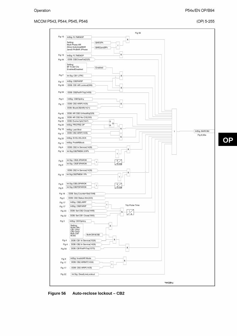
&IntSig: BARCB2
S
RQ
&DDB: CB1 AR Lockout(306)
DDB: AR CB2 Unhealthy(329)
DDB: AR CB2 No C/S(330)
DDB: CB2 ARIP(1435)
DDB: CB2FailPrTrip(1459)
DDB: CB2CloseFail(325)
DDB: BlockCB2AR(1421)
DDB: Evolve 3ph(1547)
Int Sig: CB1 LFRC
BAR3Ph
BAR2and3Ph
Setting:Multi Phase AR:Allow Autoclose/BAR 2and3 Ph/BAR 3Phase
EnabledSetting:BF if Lfail Cls:Enabled/Disabled
DDB: CB2 In Service(1428)
Int Sig:CB2TMEM 2/3Ph
Int Sig: CB2L3PAROK
Int Sig: CB2F3PAROK
1
&
100.02s
DDB: CB2 In Service(1428)
Int Sig:CB2TMEM 1Ph
Int Sig:CB2LSPAROK
Int Sig:CB2FSPAROK
1
&
1 00.02s
Fig 56
Fig 8,56a
Fig 15
Fig 15
Fig 44
Fig 7
Fig 17
Fig 55
Fig 54
Fig 40
Fig 40Fig 20
Fig 20
Fig 18
Fig 17
Fig 20
Fig 11
Fig 4
Fig 14
Fig 9
Fig 9
Fig 14
Fig 9
Fig 9
DDB: Seq Counter>Set(1546)Fig 18
DDB: CB2 Status Alm(323)Fig 2
DDB: CB2 ARIP(1435)
IntSig: CB2OpAnyFig 3
Fig 17 &
IntSig: CB2LAIRPFig 17
IntSig: CB2FARIPFig 17
IntSig: CB1OpAnyFig 3
DDB: Set CB2 Close(1449)Fig 33
DDB: Set CB1 Close(1565)Fig 32
1
& t0
Trip Pulse Time
Setting:NUM CBs : CB1 Only/CB2 Only/ Both CB1&CB2 BothCB1&CB2
DDB: CB1 In Service(1526)Fig 4
DDB: CB2 In Service(1428)Fig 4
&
&DDB: CB1FailPrTrip(1575)Fig 54
1
&
DDB: CB2 ARINIT(1434)&
IntSig: InvalidAR ModeFig 9
Fig 171
DDB: CB2 ARIP(1435)Fig 17
Int Sig: DeadLineLockoutFig 22
Figure 56 Auto-reclose lockout – CB2

P54x/EN OP/B94 Operation (OP) 5-256
MiCOM P543, P544, P545, P546
OP
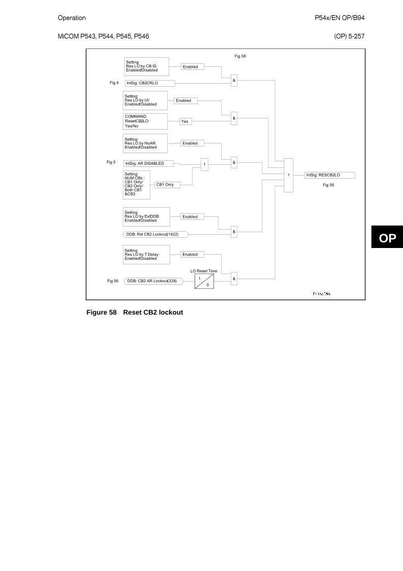
IntSig: RESCB2LO
IntSig: BARCB2
&
S
RQ
&
1
&
DDB: CB2 AR Lockout(328)Setting:NUM CBs : CB1 Only/CB2 Only/ Both CB1&CB2 BothCB1&CB2
CB2 Only
Fig 56a
Fig 56
Fig 4,8,10,20,27,33,40,42,5
5,58
Fig 58
DDB: AR In Service(1385)Fig 5
Auto-reclose lockout – CB2
P4154ENa
&IntSig: CB1CRLO
COMMAND: ResetCB1LO:Yes/No
1 IntSig: RESCB1LO
&
&
Yes
DDB: Rst CB1 Lockout(446)
t0
LO Reset Time
&
&
1
DDB: CB1AR Lockout(306)
Setting:Res LO by CB IS:Enabled/Disabled
Enabled
EnabledSetting:Res LO by UI:Enabled/Disabled
EnabledSetting:Res LO by NoAR:Enabled/Disabled
Setting:NUM CBs : CB1 Only/CB2 Only/ Both CB1&CB2
CB2 Only
EnabledSetting:Res LO by ExtDDB:Enabled/Disabled
EnabledSetting:Res LO by T Delay:Enabled/Disabled
Fig 57
Fig 55
Fig 4
Fig 5
Fig 55
IntSig: AR DISABLED
Figure 57 Reset CB1 lockout
Operation P54x/EN OP/B94 MiCOM P543, P544, P545, P546
(OP) 5-257
OP
&IntSig: CB2CRLO
1 IntSig: RESCB2LO
&
&
DDB: Rst CB2 Lockout(1422)
t
0
LO Reset Time
&
&
1
DDB: CB2 AR Lockout(328)
Setting:Res LO by CB IS:Enabled/Disabled
Enabled
COMMAND: ResetCB2LO:Yes/No
Yes
EnabledSetting:Res LO by UI:Enabled/Disabled
EnabledSetting:Res LO by NoAR:Enabled/Disabled
Setting:NUM CBs : CB1 Only/CB2 Only/ Both CB1&CB2
CB1 Only
EnabledSetting:Res LO by ExtDDB:Enabled/Disabled
EnabledSetting:Res LO by T Delay:Enabled/Disabled
Fig 56
Fig 58
Fig 4
Fig 5
Fig 56
IntSig: AR DISABLED
Figure 58 Reset CB2 lockout
P54x/EN OP/B94 Operation (OP) 5-258
MiCOM P543, P544, P545, P546
OP
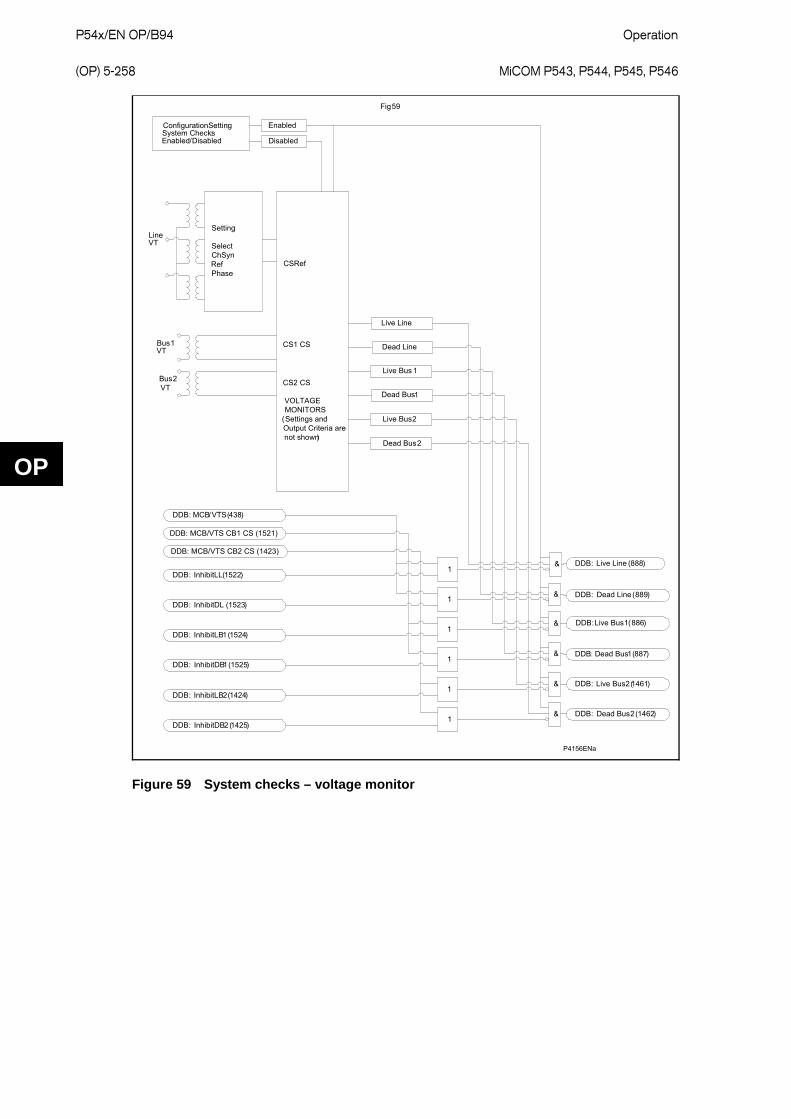
P4156ENa
CSRef
CS1 CS
VOLTAGEMONITORS
(Settings and Output Criteria are not shown)
DDB: MCB/VTS(438)
1&
DDB: MCB/VTS CB1 CS (1521)
Setting:
SelectChSynRefPhase
DDB: InhibitLL(1522)
DDB: InhibitDL (1523)
DDB: InhibitLB1(1524)
DDB: InhibitDB1(1525)
DDB: InhibitLB2(1424)
DDB: InhibitDB2 (1425)
DDB: Dead Line (889)
DDB: Live Bus1(886)
DDB: Dead Bus1(887)
DDB: Live Bus2(1461)
DDB: Dead Bus2(1462)
&
&
&
&
&
1
1
1
1
1
Line VT
Bus1 VT
Bus2 VT
Enabled
Disabled
Live Line
Dead Line
Live Bus 1
Dead Bus1
Live Bus2
Dead Bus2
DDB: Live Line (888)
ConfigurationSetting:System Checks:Enabled/Disabled
Fig 59
CS2 CS
DDB: MCB/VTS CB2 CS (1423)
Figure 59 System checks – voltage monitor

Operation P54x/EN OP/B94 MiCOM P543, P544, P545, P546
(OP) 5-259
OP
CSRef
Check Synch
Check synch settings and operation criteria are shown
1
Setting:
SelectA-N,B-N,C-NA-B,B-C,C-A
DDB:CB1 CS1 OK(883)
DDB:CB1 CS1 Enabled(881)*
DDB:CB1 CS2 Enabled(882)*
DDB: CSVLine>(1581)
DDB: CSVBus1>(1583)
DDB: CB1 CS1 VL>VB(1586)
DDB: CB1 CS1 VL<VB(1588)
DDB: CB1 CS1 FL>FB(1590)
DDB: CB1 CS1 FL<FB(1591)
& DDB: CB1 CS1SlipF>(1578)
DDB: CB1 CS1SlipF<(1579)
DDB: CB1 CS2SlipF>(1464)
DDB: CB1 CS2SlipF<(1465)
DDB: CSVline<(1580)
DDB: CSVBus1<(1582)
DDB: CB1 CS2 FL>FB(1493)
DDB: CB1 CS2 FL<FB(1494)
DDB: CB1 CS2AngHigh+(1495)
DDB: CB1 CS2AngHigh-(1496)
DDB: CB1 CS AngRotACW(1594)
DDB: CB1 CS AngRotCW(1595)
DDB: CB1 CS1AngHigh+(1592)
DDB: CB1 CS1AngHigh-(1593)
&
&
&
&
&
&
&
&
&
&
&
&
&
&
&
&
&
&
&
CB1 CS1SlipF>
CB1 CS1SlipF<
CB1 CS2SlipF>
CB1 CS2SlipF<
CSVline<
CSVBus1<
CSVLine>
CSVBus1>
CB1 CS1VL>VB1
CB1 CS1VL<VB1
CB1 CS1FL>FB1
CB1 CS1FL<FB1
CB1 CS1AngHigh+
CB1 CS1AngHigh-
CB1 CS2FL>FB1
CB1 CS2FL<FB1
CB1 CS2AngHigh+
CB1 CS2AngHigh-
CS1AngRotACW
CS1AngRotCW
DDB: CB1 CS2 VL>VB(1587)
DDB: CB1 CS2 VL<VB(1589)
&
&
CB1 CS2VL>VB1
CB1 CS2VL<VB1
&
&
Setting:System Checks CB1:Enabled/Disabled
Enabled
Disabled
DDB:SchkslnactiveCB1(880)
Setting:CB1 CS1:Enabled/Disabled
Enabled
Disabled&
Setting:CB1 CS2:Enabled/Disabled
Enabled
Disabled&
BUS1 VT
LINE VT
CS1
Inputs default to high if unmapped in PSL
CB1 CS1CriteriaOK
CB1 CS2CriteriaOK
DDB:CB1 CS2 OK(884)
ConfigurationSetting:System Checks:Enabled/Disabled
Enabled
Disabled 1
&
DDB: MCB/VTS(438)
DDB: MCB/VTSCS1(1521)
DDB: F Out of Range(319)
Fig 60
DDB: VTS Fast Block(832)
*Note If not mapped in PSL are defaulted high.
Figure 60 CB1 synch check signals
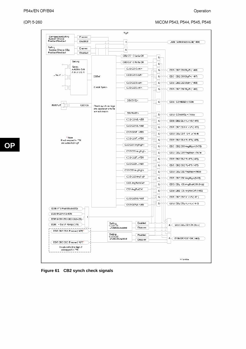
P54x/EN OP/B94 Operation (OP) 5-260
MiCOM P543, P544, P545, P546
OP
Figure 61 CB2 synch check signals
Operation P54x/EN OP/B94 MiCOM P543, P544, P545, P546
(OP) 5-261
OP
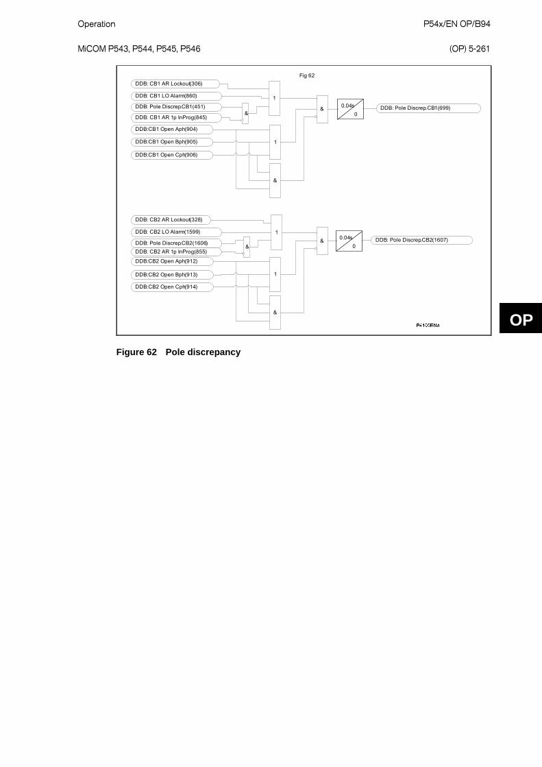
DDB: Pole Discrep.CB1(451)1
&
1
&
DDB: Pole Discrep.CB1(699)0.04s0
DDB: Pole Discrep.CB2(1606) &
1
&
DDB: Pole Discrep.CB2(1607)0.04s0
DDB:CB2 Open Aph(912)
DDB:CB2 Open Bph(913)
DDB:CB2 Open Cph(914)
DDB:CB1 Open Aph(904)
DDB:CB1 Open Bph(905)
DDB:CB1 Open Cph(906)
DDB: CB1 LO Alarm(860)
DDB: CB2 LO Alarm(1599)
DDB: CB2 AR Lockout(328)
DDB: CB1 AR Lockout(306)Fig 62
&DDB: CB1 AR 1p InProg(845)
1
&DDB: CB2 AR 1p InProg(855)
Figure 62 Pole discrepancy

P54x/EN OP/B94 Operation (OP) 5-262
MiCOM P543, P544, P545, P546
OP
DDB: Trip Inputs A (530)
DDB: Trip Inputs B (531)
DDB: Trip Inputs C (532)
DDB: Force 3PTrip CB1(533)
DDB: CB1 Trip I/P 3ph(529)
1
1
1
S
RQ
S
RQ
S
RQ
1
1 S
RQ
Setting: CB1 TripMode
3 P 1 /3P
&
DDB: CB1 Trip Output A(523)
DDB: CB1Trip Output B(524)
DDB: CB1 Trip Output C(525)
DDB: CB1 Trip 3Ph(526)
DDB: Force 3PTrip CB2(1604)
DDB: CB2 Trip I/P 3ph(1608)
1
Setting: CB2 TripMode
3 P 1 /3P
&S
RQ DDB: CB2 Trip 3Ph (1600)
1
1
1
S
RQ
S
RQ
S R
Q
DDB: CB2 Trip Output A (1601)
DDB: CB2Trip Output B (1602)
DDB: CB2 Trip Output C (1603)
1 Dwell100ms
DDB: Any Trip(522)
3P
3P
DDB: PoledeadA(892)
DDB: PoledeadB(893)
DDB: PoledeadC(894)
1
1
1
&
&
&
1
&
2
S
RQ DDB: 2/3Ph Fault(527)
S
RQ DDB: 3Ph Fault(528)
DDB: AR Force CB1 3P(858)
DDB: AR Force CB2 3P(1485) 1
1
Fig 63
P4160ENa
Figure 63 CB trip conversion

Operation P54x/EN OP/B94 MiCOM P543, P544, P545, P546
(OP) 5-263
OP
7. P544/P546 CIRCUIT BREAKER CONTROL AND AUTO-RECLOSE LOGIC: INTERNAL SIGNAL DEFIN ITIONS The breaker control functionality of the P544/P546 is described in the figures in the previous section. Within that description a number of signals that are internal to the logic of the circuit breaker control are featured. Unlike the DDB signals, these internal signals cannot be accessed using the programmable scheme logic. They are hard-coded into the application software. This section lists those signals and provides a brief description to aid understanding.
Note: This section lists only the hard-coded internal signals used in the circuit breaker control. The DDB signals featuring in the logic are described in the programmable logic chapter (P54x_EN_PL) of this manual.
Name Description
3PDTCOMP Int Sig: Three phase dead time complete
AR DISABLED Int Sig: Overall autoreclosing disabled
BAR CB1 Int Sig from “Autoreclose Lockout – CB1”
BAR CB2 Int Sig from “Autoreclose Lockout – CB2”
CB1 3PDTCOMP Int Sig: CB1 3PAR dead time complete
CB1 3PFTCOMP Int Sig: CB1 3PAR follower time complete
CB1 3POK Int Sig: CB1 OK for 3P AR (leader or follower)
CB1 ARSUCC Int Sig: CB1 auto-reclose sucessful
CB1 CS1 AngHigh- Int Sig + DDB: Line/Bus1 phase angle in range: -CB1 CS1 Angle to -180deg
CB1 CS1 AngHigh+ Int Sig + DDB: Line/Bus1 phase angle in range: +CB1 CS1 Angle to +180deg
CB1 CS1 FL<FB Int Sig + DDB: Bus1 F > (Line F + “CB1 CS1 SlipFreqf”)
CB1 CS1 FL>FB Int Sig + DDB: Line F > (Bus1 F + “CB1 CS1 SlipFreqf”)
CB1 CS1 OK Int Sig + DDB: CB1 CS1 is enabled and Line and Bus 1 voltages meet CB1 CS1 settings
CB1 CS1 SlipF< Int Sig + DDB: Line-Bus 1 slip freq < CB1 CS1 SlipFreq setting
CB1 CS1 SlipF> Int Sig + DDB: Line-Bus 1 slip freq > CB1 CS1 SlipFreq setting
CB1 CS1 VL<VB Int Sig + DDB: Bus1 V > (Line V + “CB1 CS1 VDiff”)
CB1 CS1 VL>VB Int Sig + DDB: Line V > (Bus1 V + “CB1 CS1 VDiff”)
CB1 CS2AngHigh- Int Sig + DDB: Line/Bus1 phase angle in range: -CB1 CS2 Angle to -180deg

P54x/EN OP/B94 Operation (OP) 5-264
MiCOM P543, P544, P545, P546
OP
Name Description
CB1 CS2AngHigh+ Int Sig + DDB: Line/Bus1 phase angle in range: +CB1 CS2 Angle to +180deg
CB1 CS2FL<FB Int Sig + DDB: Bus1 F > (Line F + “CB1 CS2 SlipFreqf”)
CB1 CS2FL>FB Int Sig + DDB: Line F > (Bus1 F + “CB1 CS2 SlipFreqf”)
CB1 CS2OK Int Sig + DDB: CB1 CS2 is enabled and Line and Bus 1 voltages meet CB1 CS2 settings
CB1 CS2SlipF< Int Sig + DDB: Line-Bus 1 slip freq < CB1 CS2 SlipFreq setting
CB1 CS2SlipF> Int Sig + DDB: Line-Bus 1 slip freq > CB1 CS2 SlipFreq setting
CB1 CS2VL<VB Int Sig + DDB: Bus1 V > (Line V + “CB1 CS2 VDiff”)
CB1 CS2VL>VB Int Sig + DDB: Line V > (Bus1 V + “CB1 CS2 VDiff”)
CB1 FARIP Int Sig : CB1 ARIP as follower
CB1 LARIP Int Sig : CB1 ARIP as leader
CB1 Op1P Int Sig: CB1 open single phase
CB1 Op2/3P Int Sig: CB1 open on 2 or 3 phases
CB1 OpAny Int Sig: CB1 open on 1, 2 or 3 phases
CB1 SPOK Int Sig: CB1 OK for SP AR (leader or follower)
CB1 SysCh Off Int Sig + DDB: CB1 CS1 & CB1 CS2checks disabled
CB1CRLO Int Sig: CB1 in service – reset CB1 lockout
CB1F3PAR Int Sig from “Three Phase AR Cycle Selection”
CB1F3PAROK Int Sig: CB1 OK to 3Ph AR as follower
CB1FSPAR Int Sig: CB1 SPAR in progress as follower
CB1FSPAROK Int Sig: CB1 OK to SP AR as follower
CB1L3PAR Int Sig from “Three Phase AR Cycle Selection”
CB1L3PAR Int Sig from “Single Phase AR Cycle Selection”
CB1L3PAROK Int Sig: CB1 OK to 3Ph AR as leader
CB1LFRC Int Sig: CB1 failed to reclose as leader
CB1LFRC Int Sig from “Leader/Follower Logic – 1”
CB1LSPAR Int Sig from “Single Phase AR Cycle Selection”
CB1LSPAROK Int Sig: CB1 OK to SP AR as leader
CB1SPDTCOMP Int Sig: CB1 SP dead time complete
CB1SPFTCOMP Int Sig: CB1 SP follower time complete

Operation P54x/EN OP/B94 MiCOM P543, P544, P545, P546
(OP) 5-265
OP
Name Description
CB2 3PDTCOMP Int Sig: CB2 3PAR dead time complete
CB2 3PFTCOMP Int Sig: CB2 3PAR follower time complete
CB2 3POK Int Sig: CB2 OK for 3P AR (leader or follower)
CB2 ARSUCC Int Sig: CB2 auto-reclose sucessful
CB2 CS1 AngHigh- Int Sig + DDB: Line/Bus2 phase angle in range: -CB2 CS1 Angle to -180deg
CB2 CS1 AngHigh+ Int Sig + DDB: Line/Bus2 phase angle in range: +CB2 CS1 Angle to +180deg
CB2 CS1 FL<FB Int Sig + DDB: Bus2 F > (Line F + “CB2 CS1 SlipFreqf”)
CB2 CS1 FL>FB Int Sig + DDB: Line F > (Bus2 F + “CB2 CS1 SlipFreqf”)
CB2 CS1 OK Int Sig + DDB: CB2 CS1 is enabled and Line and Bus 2 voltages meet CB2 CS1 settings
CB2 CS1 SlipF< Int Sig + DDB: Line-Bus 2 slip freq < CB2 CS1 SlipFreq setting
CB2 CS1 SlipF> Int Sig + DDB: Line-Bus 2 slip freq > CB2 CS1 SlipFreq setting
CB2 CS1 VL<VB Int Sig + DDB: Bus2 V > (Line V + “CB2 CS1 VDiff”)
CB2 CS1 VL>VB Int Sig + DDB: Line V > (Bus2 V + “CB2 CS1 VDiff”)
CB2 CS2AngHigh- Int Sig + DDB: Line/Bus2 phase angle in range: -CB2 CS2 Angle to -180deg
CB2 CS2AngHigh+ Int Sig + DDB: Line/Bus2 phase angle in range: +CB2 CS2 Angle to +180deg
CB2 CS2FL<FB Int Sig + DDB: Bus2 F > (Line F + “CB2 CS2 SlipFreqf”)
CB2 CS2FL>FB Int Sig + DDB: Line F > (Bus2 F + “CB2 CS2 SlipFreqf”)
CB2 CS2OK Int Sig + DDB: CB2 CS2 is enabled and Line and Bus 2 voltages meet CB2 CS2 settings
CB2 CS2SlipF< Int Sig + DDB: Line-Bus 2 slip freq < CB2 CS2 SlipFreq setting
CB2 CS2SlipF> Int Sig + DDB: Line-Bus 2 slip freq > CB2 CS2 SlipFreq setting
CB2 CS2VL<VB Int Sig + DDB: Bus2 V > (Line V + “CB2 CS2 VDiff”)
CB2 CS2VL>VB Int Sig + DDB: Line V > (Bus2 V + “CB2 CS2 VDiff”)
CB2 FARIP Int Sig: CB2 ARIP as follower

P54x/EN OP/B94 Operation (OP) 5-266
MiCOM P543, P544, P545, P546
OP
Name Description
CB2 LARIP Int Sig: CB2 ARIP as leader
CB2 Op1P Int Sig: CB2 open single phase
CB2 Op2/3P Int Sig: CB2 open on 2 or 3 phases
CB2 OpAny Int Sig: CB2 open on 1, 2 or 3 phases
CB2 SPOK Int Sig: CB2 OK for SP AR (leader or follower)
CB2 SysCh Off Int Sig + DDB: CB2 CS1 & CB2 CS2checks disabled
CB2 TAR 2/3Ph Int Sig: 2Ph or 3Ph trip & AR initiation CB2
CB2 TARA Int Sig: A Ph trip & AR initiation CB2
CB2 TARB Int Sig: B Ph trip & AR initiation CB2
CB2 TARC Int Sig: C Ph trip & AR initiation CB2
CB2 TMEM 1Ph Int Sig: CB1 1Ph trip +AR AR initiation memory CB2
CB2 TMEM 2/3Ph Int Sig: CB1 2Ph trip +AR AR initiation memory CB2
CB2 TMEM 3Ph Int Sig: CB1 3Ph trip +AR AR initiation memory CB2
CB2CRLO Int Sig: CB2 in service – reset CB2 lockout
CB2F3PAR Int Sig from “Three Phase AR Cycle Selection”
CB2F3PAROK Int Sig: CB2 OK to 3Ph AR as follower
CB2FSPAR Int Sig: CB2 SPAR in progress as follower
CB2FSPAROK Int Sig: CB2 OK to SP AR as follower
CB2L3PAR Int Sig from “Three Phase AR Cycle Selection”
CB2L3PAROK Int Sig: CB2 OK to 3Ph AR as leader
CB2LFRC Int Sig: CB2 failed to reclose as leader
CB2LFRC Int Sig from “Leader/Follower Logic – 1”
CB2LSPAR Int Sig from “Single Phase AR Cycle Selection”
CB2LSPAROK Int Sig: CB2 OK to SP AR as leader
CB2SPDTCOMP Int Sig: CB2 SP dead time complete
CB2SPFTCOMP Int Sig: CB2 SP follower time complete
CBARCancel Int Sig: Stop and reset CB1 and CB2 AR In progress
CS VBus1< Int Sig + DDB: Bus1 Volts < CS UV setting
CS VBus1> Int Sig + DDB: Bus1 Volts > CS OV setting
CS VBus2< Int Sig + DDB: Bus2 Volts < CS UV setting
CS VBus2> Int Sig + DDB: Bus2 Volts > CS OV setting
CS VLine< Int Sig + DDB: Line Volts < CS UV setting
CS VLine> Int Sig + DDB: Line Volts > CS OV setting

Operation P54x/EN OP/B94 MiCOM P543, P544, P545, P546
(OP) 5-267
OP
Name Description
CS1 Ang Rot ACW Int Sig + DDB: Line freq > (Bus1 freq + 0.001Hz) (CS1 Angle Rotating Anticlockwise)
CS1 Ang Rot CW Int Sig + DDB: Bus1 freq > (Line freq + 0.001Hz) (CS1 Angle Rotating Clockwise)
CS2 Ang Rot ACW Int Sig + DDB: Line freq > (Bus2 freq + 0.001Hz) (CS2 Angle Rotating Anticlockwise)
CS2 Ang Rot CW Int Sig + DDB: Bus2 freq > (Line freq + 0.001Hz) (CS2 Angle Rotating Clockwise)
Dead Bus 1 Int Sig + DDB: CS1 V magnitude < Dead Bus 1 setting
Dead Bus 2 Int Sig + DDB: CS2 V magnitude < Dead Bus 2 setting
Dead Line Int Sig + DDB: Line V magnitude < Dead Line setting
DeadLineLockout Int Sig: When setting “3PDT Start When LD” is set to Enabled and the line does not go dead for a time set by “Dead Line Time” then this signal will force the auto-reclose sequence to lockout.
ENABLE CB13PDT Int Sig: Enable dead time for CB1 3PAR
ENABLE CB1SPDT Int Sig: Enable dead time for CB1 SPAR
ENABLE CB23PDT Int Sig: Enable dead time for CB2 3PAR
ENABLE CB2SPDT Int Sig: Enable dead time for CB2 SPAR
EVOLVE LOCK Int Sig: Lockout for 2nd trip after Discrim Tim
F Out of Range Int Sig from frequency tracking logic
FLTMEM 2P Int Sig: 2 Ph fault memory
FLTMEM 3P Int Sig: 3 Ph fault memory
Foll CB1 Int Sig from “Leader & Follower Logic – 2”
Foll CB2 Int Sig from “Leader & Follower Logic – 2”
Foll3PAROK Int Sig from “Leader & Follower AR Modes Enable”
FollSPAROK Int Sig from “Leader & Follower AR Modes Enable”
INIT AR Int Sig: Host protection required to initiate AR
Invalid AR Mode Int Sig: An invalid state is being indicated by the logic that determines AR mode by opto.
Last Shot Int Sig: the last shot
Live Bus 1 Int Sig + DDB: CS1 V magnitude >= Live Bus 1 setting

P54x/EN OP/B94 Operation (OP) 5-268
MiCOM P543, P544, P545, P546
OP
Name Description
Live Bus 2 Int Sig + DDB: CS2 V magnitude >= Live Bus 2 setting
Live Line Int Sig + DDB: Line V magnitude >= Live Line setting
OK Time SP Int Sig from “Single Phase AR Lead CB Dead Time”
PrefLCB1 Int Sig: CB1 is the preferred leader
PrefLCB2 Int Sig: CB2 is the preferred leader
Prot AR Block* Int Sig: Host protection required to block AR
Prot Re-op Int Sig from “Protection Re-operation + Evolving Fault”
RESCB1ARSUCC Int Sig from “Reset CB1 Successful AR Indication
RESCB1LO Int Sig from “Reset CB1 Lockout”
RESCB2ARSUCC Int Sig from “Reset CB2 Successful AR Indication
RESCB2LO Int Sig from “Reset CB2 Lockout”
Reset L-F Int Sig: From “Protection Re-operation + Evolving fault”
RESPRMEM Int Sig: Reset “trip & AR” memory
SC Increment Int Sig: Increment the sequence counter
SCCountoveqShots Int Sig: Sequence counter has exceeded setting
SET CB1CL Int Sig from “CB1 Auto Close”
SET CB2CL Int Sig from “CB2 Auto Close”
SET LCB1 Int Sig: CB1 selected leader
SET LCB1 Int Sig from “Leader/Follower Logic – 1”
SET LCB2 Int Sig: CB2 selected leader
SET LCB2 Int Sig from “Leader/Follower Logic – 1”
SETCB13PCL Int Sig: CB1 three phase close given
SETCB1SPCL Int Sig: CB1 single phase close given
SETCB23PCL Int Sig: CB2 three phase close given
SETCB2SPCL Int Sig: CB2 single phase close given
SPDTCOMP Int Sig: Single phase dead time complete
TAR 2/3Ph Int Sig: 2Ph or 3Ph trip & AR initiation
TARA Int Sig: A Ph trip & AR initiation
TARANY Int Sig from “CB1 1 Pole / 3 Pole Trip + AR Initiation”
TARANY Int Sig: Any trip & AR initiation
TARB Int Sig: B Ph trip & AR initiation
TARC Int Sig: C Ph trip & AR initiation
Operation P54x/EN OP/B94 MiCOM P543, P544, P545, P546
(OP) 5-269
OP
Name Description
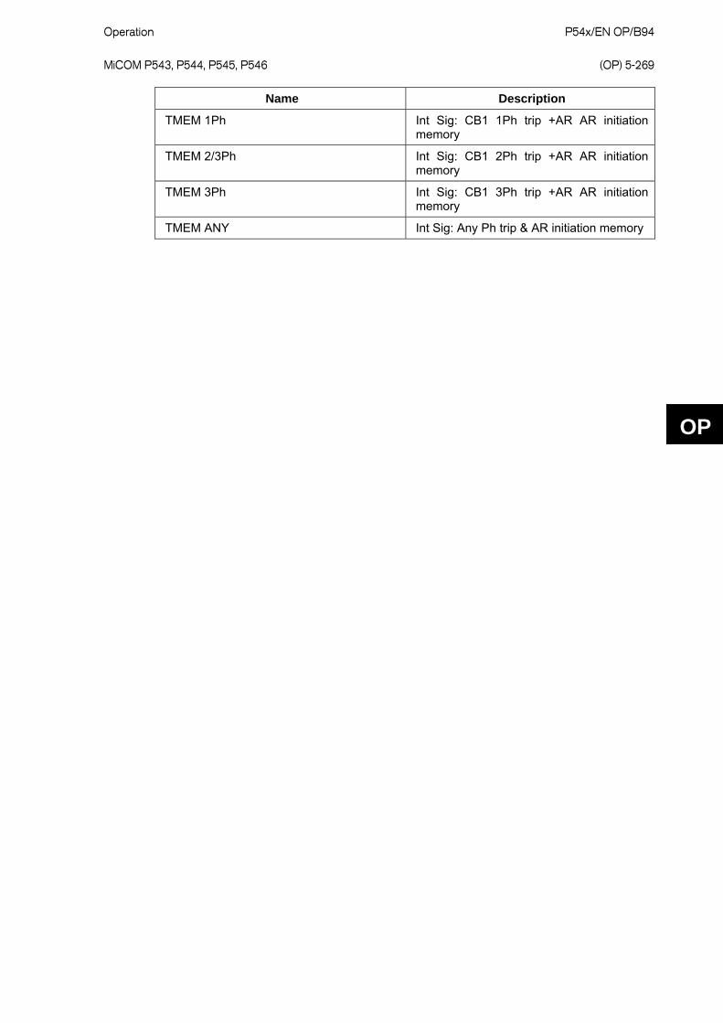
TMEM 1Ph Int Sig: CB1 1Ph trip +AR AR initiation memory
TMEM 2/3Ph Int Sig: CB1 2Ph trip +AR AR initiation memory
TMEM 3Ph Int Sig: CB1 3Ph trip +AR AR initiation memory
TMEM ANY Int Sig: Any Ph trip & AR initiation memory
P54x/EN OP/B94 Operation (OP) 5-270
MiCOM P543, P544, P545, P546
OP

Application Notes P54x/EN AP/Ja4 MiCOM P543, P544, P545 & P546
AP
APPLICATION NOTES
Date: 16th March 2009 Hardware suffix: K Software versions:
45 (P543/4/5/6 without Distance) 55 (P543/4/5/6 with Distance)
Connection diagrams:
10P54302 (SH 1 to 2) 10P54303 (SH 1 to 2)
10P54400 10P54404 (SH 1 to 2) 10P54405 (SH 1 to 2)
10P54502 (SH 1 to 2) 10P54503 (SH 1 to 2)
10P54600 10P54604 (SH 1 to 2) 10P54605 (SH 1 to 2) 10P54606 (SH 1 to 2)

P54x/EN AP/Ja4 Application Notes
MiCOM P543, P544, P545 & P546
AP

Application Notes P54x/EN AP/Ja4 MiCOM P543, P544, P545 & P546
(AP) 6-1
AP
CONTENTS
(AP) 6-
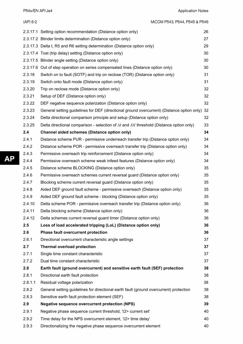
1. INTRODUCTION 7 1.1 Protection of overhead line, cable, and hybrid circuits 7
2. APPLICATION OF INDIVIDUAL PROTECTION FUNCTIONS 9 2.1 Differential protection 9 2.1.1 Setting of the phase differential characteristic 9 2.1.2 Relay sensitivity under heavy load conditions 10 2.1.3 CT ratio correction (all models) 11 2.1.4 Transformers in zone applications (P543 & P545 models) 11 2.1.4.1 CT ratio correction 12 2.1.4.2 Phase correction and zero sequence current filtering 12 2.1.4.3 High set differential setting 13 2.1.5 Mesh corner and 1½ breaker switched substations 13 2.1.6 Small tapped loads (tee feeds) 13 2.2 Optional distance protection 14 2.3 Distance protection and aided DEF (Distance option only) 14 2.3.1 Simple and advanced setting mode (Distance option only) 14 2.3.2 Line parameters settings (Distance option only) 14 2.3.3 Residual compensation for earth/ground faults (Distance option only) 14 2.3.4 Mutual compensation for parallel lines (Distance option only) 14 2.3.5 Selection of distance operating characteristic (Distance option only) 15 2.3.5.1 Phase characteristic (Distance option only) 15 2.3.5.2 Ground characteristic (Distance option only) 16 2.3.6 Zone reaches - recommended settings (Distance option only) 16 2.3.7 Quadrilateral phase resistive reaches (Distance option only) 17 2.3.8 Quadrilateral ground resistive reaches and tilting (Distance option only) 18 2.3.9 Phase fault zone settings (Distance option only) 20 2.3.10 Distance directional principle and setup (Distance option only) 20 2.3.11 Delta directional - selection of RCA (Distance option only) 20 2.3.12 Distance setup - filtering, load blinding and polarizing (Distance option only) 21 2.3.12.1 Digital filtering (Distance option only) 21 2.3.12.2 CVTs with passive suppression of ferroresonance (Distance option only) 21 2.3.12.3 CVTs with active suppression of ferroresonance (Distance option only) 21 2.3.13 Load blinding (load avoidance) (Distance option only) 21 2.3.13.1 Recommended polarizing settings (Distance option only) 22 2.3.14 Distance elements basic scheme setting (Distance option only) 22 2.3.15 Power swing alarming and blocking (Distance option only) 23 2.3.16 Out of step protection (Distance option only) 24 2.3.17 Critical stability angle (Distance option only) 24
P54x/EN AP/Ja4 Application Notes (AP) 6-2
MiCOM P543, P544, P545 & P546
AP
2.3.17.1 Setting option recommendation (Distance option only) 26 2.3.17.2 Blinder limits determination (Distance option only) 27 2.3.17.3 Delta t, R5 and R6 setting determination (Distance option only) 29 2.3.17.4 Tost (trip delay) setting (Distance option only) 30 2.3.17.5 Blinder angle setting (Distance option only) 30 2.3.17.6 Out of step operation on series compensated lines (Distance option only) 30 2.3.18 Switch on to fault (SOTF) and trip on reclose (TOR) (Distance option only) 31 2.3.19 Switch onto fault mode (Distance option only) 31 2.3.20 Trip on reclose mode (Distance option only) 32 2.3.21 Setup of DEF (Distance option only) 32 2.3.22 DEF negative sequence polarization (Distance option only) 32 2.3.23 General setting guidelines for DEF (directional ground overcurrent) (Distance option only) 32 2.3.24 Delta directional comparison principle and setup (Distance option only) 32 2.3.25 Delta directional comparison - selection of ΔI and ΔV threshold (Distance option only) 33 2.4 Channel aided schemes (Distance option only) 34 2.4.1 Distance scheme PUR - permissive underreach transfer trip (Distance option only) 34 2.4.2 Distance scheme POR - permissive overreach transfer trip (Distance option only) 34 2.4.3 Permissive overreach trip reinforcement (Distance option only) 34 2.4.4 Permissive overreach scheme weak infeed features (Distance option only) 34 2.4.5 Distance scheme BLOCKING (Distance option only) 35 2.4.6 Permissive overreach schemes current reversal guard (Distance option only) 35 2.4.7 Blocking scheme current reversal guard (Distance option only) 35 2.4.8 Aided DEF ground fault scheme - permissive overreach (Distance option only) 35 2.4.9 Aided DEF ground fault scheme - blocking (Distance option only) 35 2.4.10 Delta scheme POR - permissive overreach transfer trip (Distance option only) 36 2.4.11 Delta blocking scheme (Distance option only) 36 2.4.12 Delta schemes current reversal guard timer (Distance option only) 36 2.5 Loss of load accelerated tripping (LoL) (Distance option only) 36 2.6 Phase fault overcurrent protection 36 2.6.1 Directional overcurrent characteristic angle settings 37 2.7 Thermal overload protection 37 2.7.1 Single time constant characteristic 37 2.7.2 Dual time constant characteristic 37 2.8 Earth fault (ground overcurrent) and sensitive earth fault (SEF) protection 38 2.8.1 Directional earth fault protection 38 2.8.1.1 Residual voltage polarization 38 2.8.2 General setting guidelines for directional earth fault (ground overcurrent) protection 38 2.8.3 Sensitive earth fault protection element (SEF) 38 2.9 Negative sequence overcurrent protection (NPS) 39 2.9.1 Negative phase sequence current threshold, 'Ι2> current set' 40 2.9.2 Time delay for the NPS overcurrent element, ‘Ι2> time delay’ 40 2.9.3 Directionalizing the negative phase sequence overcurrent element 40

Application Notes P54x/EN AP/Ja4 MiCOM P543, P544, P545 & P546
(AP) 6-3
AP
2.10 Undervoltage protection 40 2.11 Overvoltage protection 41 2.12 Compensated overvoltage protection 41 2.13 Residual overvoltage (neutral displacement) protection 42 2.13.1 Setting guidelines 44 2.14 Circuit breaker fail protection (CBF) 44 2.14.1 Breaker fail timer settings 44 2.14.2 Breaker fail undercurrent settings 44 2.15 Broken conductor detection 45 2.15.1 Setting guidelines 45 2.16 Communication between relays 46 2.16.1 Optical budgets 46 2.16.2 Clock source setting 47 2.16.3 Data rate 47 2.17 InterMiCOM64 (“Fiber InterMiCOM”) 47 2.17.1 IMx command type 47 2.17.2 IMx fallback mode 48
3. WORKED PROTECTION EXAMPLE AND OTHER PROTECTION TIPS 49 3.1 Differential protection setting examples 49 3.1.1 Differential element 49 3.1.2 Transformer feeder examples 50 3.1.3 Teed feeder example 51 3.1.4 Three winding transformer in zone with different rated CTs example 53 3.2 Distance protection setting example 55 3.2.1 Objective 55 3.2.2 System data 56 3.2.3 Relay settings 56 3.2.4 Line impedance 56 3.2.5 Residual compensation for ground fault elements 56 3.2.6 Zone 1 phase and ground reach settings 57 3.2.7 Zone 2 phase and ground reach settings 57 3.2.8 Zone 3 phase and ground reach settings 57 3.2.9 Zone 3 reverse reach 57 3.2.10 Load avoidance 58 3.2.11 Additional settings for quadrilateral applications 58 3.2.11.1 Phase fault resistive reaches (Rph) 58 3.2.11.2 Ground fault resistive reaches (RGnd) 59 3.3 Teed feeder protection 59 3.3.1 The apparent impedance seen by the distance elements 59 3.3.2 Permissive overreach schemes 60 3.3.3 Permissive underreach schemes 60 3.3.4 Blocking schemes 61
P54x/EN AP/Ja4 Application Notes (AP) 6-4
MiCOM P543, P544, P545 & P546
AP
3.4 VT connections 62 3.4.1 Open delta (vee connected) VT's 62 3.4.2 VT single point earthing 62 3.5 Trip circuit supervision (TCS) 62 3.5.1 TCS scheme 1 63 3.5.1.1 Scheme description 63 3.5.1.2 Scheme 1 PSL 63 3.5.2 TCS scheme 2 64 3.5.2.1 Scheme description 64 3.5.2.2 Scheme 2 PSL 65 3.5.3 TCS scheme 3 65 3.5.3.1 Scheme description 65 3.5.3.2 Scheme 3 PSL 66 3.6 Intermicom64 application example 66 3.6.1 InterMiCOM64 mapping for three ended application – BLOCKING or PUR example 66 3.6.2 Intermicom64 application example general advice 68 3.6.3 Three-ended applications 68 3.6.4 Intermicom64 application example scheme description 69 3.6.5 Intermicom64 application example channel supervision 69 3.6.6 Intermicom64 application example transfer trip 70 3.6.7 InterMiCOM64 application example - mapping for two ended application 70 3.6.8 Intermicom64 application example - dual redundant communications channels 70 3.6.9 Intermicom64 application example - scheme co-ordination timers 70 3.6.9.1 InterMiCOM64 application example - distance PUR permissive underreach 70 3.6.9.2 InterMiCOM64 application example - distance POR permissive overreach 70 3.6.9.3 InterMiCOM64 application example - distance blocking 71 3.6.9.4 InterMiCOM64 application example - directional earth Fault (DEF) POR permissive overreach 71 3.6.9.5 InterMiCOM64 application example - directional earth fault (DEF) blocking 71 3.6.9.6 InterMiCOM64 application example - delta directional POR permissive overreach 71 3.6.9.7 InterMiCOM64 application example - delta directional blocking 71 3.6.10 Fallback mode for InterMiCOM64 bits 71
4. APPLICATION OF NON PROTECTION FUNCTIONS 72 4.1 Single and three phase auto-reclosing 72 4.1.1 Time delayed and high speed auto-reclosing 72 4.1.2 Auto-reclose logic operating sequence 72 4.1.3 Setting guidelines 72 4.1.3.1 Circuit breaker healthy 72 4.1.3.2 Number of shots 72 4.1.3.3 Dead timer setting 73 4.1.3.4 Follower time setting (P544 and P546 only) 73 4.1.3.5 De-ionizing time 74
Application Notes P54x/EN AP/Ja4 MiCOM P543, P544, P545 & P546
(AP) 6-5
AP
4.1.3.6 Example minimum dead time calculation 74 4.1.3.7 Reclaim timer setting 74 4.2 Current transformer supervision 75 4.2.1 Standard CTS 75 4.2.2 Differential CTS 75 4.3 Circuit breaker condition monitoring 76 4.3.1 Setting the Σ Ι^ thresholds 76 4.3.2 Setting the number of operations thresholds 76 4.3.3 Setting the operating time thresholds 76 4.3.4 Setting the excessive fault frequency thresholds 76
5. TWO CIRCUIT BREAKER CONTOL (P446) WORKED EXAMPLE 77 5.1 Introduction 77 5.2 Circuit breaker status 78 5.3 Voltage inputs 78 5.4 Application settings 78 5.4.1 CB CONTROL menu: 78 5.4.2 CONFIGURATION menu: 79 5.4.3 CT & VT RATIOS menu: 79 5.4.4 GROUP 1 LINE PARAMETERS menu: 79 5.4.5 GROUP 1 DISTANCE menu: 79 5.4.6 GROUP 1 PHASE DIFF menu: 79 5.4.7 GROUP 1 SYSTEM CHECKS menu: 80 5.4.8 GROUP 1 AUTORECLOSE menu: 81 5.5 PSL (Programmable Scheme Logic) MAPPING 82
6. CURRENT TRANSFORMER REQUIREMENTS 83 6.1 Recommended CT classes (British and IEC) 83 6.2 Current differential requirements 83 6.3 Zone 1 reach point accuracy (RPA) 84 6.4 Zone 1 close-up fault operation 84 6.5 Time delayed distance zones 84 6.6 Determining Vk for an IEEE “C" class CT 84 6.7 Worked example for CT requirements 85 6.7.1 Important notes to be considered 85 6.7.2 System data 85 6.7.3 Calculation of Primary X/R 85 6.7.4 Calculation of Source Impedance Zs 85 6.7.5 Calculation of full line impedance (full 100 kms) 86 6.7.6 Calculation of total impedance till remote bus bar 86 6.7.7 Calculation of through fault X/R 86 6.7.8 Calculation of through fault If 86 6.7.9 Calculation of line impedance till Zone1 reach point (80kms) 86

P54x/EN AP/Ja4 Application Notes (AP) 6-6
MiCOM P543, P544, P545 & P546
AP
6.7.10 Calculation of total impedance till Zone1 reach point 86 6.7.11 Calculation of X/R till Zone1 reach point 86 6.7.12 Calculation of fault current till Zone1 reach point 86 6.7.13 CT Vk for Current differential protection 87 6.7.14 CT Vk for distance Zone1 reach point 87 6.7.15 CT Vk for distance Zone1 close-up fault 87 6.7.16 CT Vk for distance time delayed zones 87 6.7.17 Vk to be considered 87
7. HIGH BREAK OUTPUT CONTACTS 88
8. AUXILIARY SUPPLY FUSE RATING 88
FIGURES Figure 1 Breaker and a half switched substation 13 Figure 2 Settings required to apply a Mho zone (Distance option only) 15 Figure 3 Settings required to apply a quadrilateral zone (Distance option only) 16 Figure 4 Example of high resistive zone 1 fault that falls outside zone 1 characteristic when the starting
tilt angle of -3° is set (over-tilting effect). (Distance option only) 18 Figure 5 Basic time stepped distance scheme (Distance option only) 23 Figure 6 Power transfer in relation to angle difference θ between 2 ends 25 Figure 7 Setting determination for the positive sequence resistive component R5 (Distance option only)27 Figure 8 R6MAX determination (Distance option only) 28 Figure 9 Example of timer reset due to MOV’s operation 31 Figure 10 Positioning of core balance current transformers 39 Figure 11 Calculated ferranti voltage rise on 345 kV and 765 kV lines 41 Figure 12 Residual voltage, solidly earthed system 42 Figure 13 Residual voltage, resistance earthed system 43 Figure 14 Typical plain feeder circuit 49 Figure 15 Typical transformer feeder circuit 50 Figure 16 Typical teed feeder application 51 Figure 17 Three winding transformer in zone application 53 Figure 18 System assumed for worked example 55 Figure 19 Teed feeder application - apparent impedances seen by RELAY 60 Figure 20 Teed feeder applications 61 Figure 21 TCS scheme 1 63 Figure 22 PSL for TCS schemes 1 and 3 64 Figure 23 TCS scheme 2 64 Figure 24 PSL for TCS scheme 2 65 Figure 25 TCS scheme 3 65 Figure 26 InterMiCOM64 mapping in a three ended application 67 Figure 27 Two circuit breaker auto-reclose application 77

Application Notes P54x/EN AP/Ja4 MiCOM P543, P544, P545 & P546
(AP) 6-7
AP
1. INTRODUCTION
1.1 Protection of overhead line, cable, and hybrid circuits
Overhead lines, typically ranging from 10 kV distribution lines to 800 kV transmission lines, are probably the most fault susceptible items of plant in a modern power system. It is therefore essential that the protection associated with them provides secure and reliable operation.
For distribution systems, continuity of supply is of paramount importance. The majority of faults on overhead lines are transient or semi-permanent in nature. Multi-shot auto-reclose cycles are therefore commonly used in conjunction with instantaneous tripping elements to increase system availability. For permanent faults it is essential that only the faulted section of plant is isolated. As such, high speed, discriminative fault clearance is often a fundamental requirement of any protection scheme on a distribution network.
The requirements for a transmission network must also take into account system stability. Where systems are not highly interconnected the use of single phase tripping and high speed auto-reclosure is often required. This in turn dictates the need for very high speed protection to reduce overall fault clearance times.
Many line configurations exist which need to be addressed. Transmission applications may typically consist of 2 or 3 terminal applications, possibly fed from breaker and a half or mesh arrangements. Lower voltage applications may again be 2 or 3 terminal configurations with the added complications of in zone transformers or small teed load transformers.
Charging current may also adversely affect protection. This is a problem particularly with cables and long transmission lines. Both the initial inrush and steady state charging current must not cause relay maloperation and preferably should not compromise protection performance.
Physical distance must be taken into account. Some EHV transmission lines can be up to several hundred kilometers in length. If high speed, discriminative protection is to be applied, it will be necessary to transfer information between line ends. This not only puts the onus on the security of signaling equipment but also on the protection in the event of loss of this signal.
Back-up protection is also an important feature of any protection scheme. In the event of equipment failure, such as signaling equipment or switchgear, for example, it is necessary to provide alternative forms of fault clearance. It is desirable to provide back-up protection which can operate with minimum time delay and yet discriminate with both the main protection and protection elsewhere on the system.
Transmission systems are essential to route power from the point of generation to the region of demand. The means of transport is generally via overhead lines, which must have maximum in-service availability. The exposed nature of overhead lines make them fault-prone, and protection devices must trip to initiate isolation of any faulted circuit. In addition to fast fault clearance to prevent plant damage, the requirements for a transmission network must also take into account system stability. Where systems are not highly interconnected the use of single phase tripping and high speed auto-reclosure is often required. This in turn dictates the need for very high speed protection to reduce overall fault clearance times.
The MiCOM P54x provides fast, highly selective protection, to trip for genuine line faults. The current differential principle easily detects intercircuit, evolving and cross country faults amongst others as the relay works on a per phase basis. It is also immune to voltage measurement problems such as CVT transients and power swings on the system and the most important benefit of all; differential principle offers the most selective line protection.
A combination with a full scheme distance protection and aided directional earth fault (DEF) makes the relay a complete and versatile solution for line protection. Differential and distance protection can be set to operate to work separately or simultaneously. Distance can also be set to work upon failure of the relay protection communications. These options allow the user to set different protection schemes such as Differential as main 1 and Distance as main 2 or vice versa, Differential as main 1 and Distance as backup, etc.
P54x/EN AP/Ja4 Application Notes (AP) 6-8
MiCOM P543, P544, P545 & P546
AP
Distance protection on MiCOM P54x offers advanced load blinding and disturbance detection techniques such as power swing blocking to ensure stability when no tripping is required. Selectable mho and quadrilateral (polygon) characteristics allow versatile deployment as main protection for all effectively-earthed transmission and distribution circuits, whether lines, cables or hybrid (a mix of part cable, part overhead line).
Back-up protection is also an important feature of any protection scheme. In the event of equipment failure, such as signaling equipment or switchgear, for example, it is necessary to provide alternative forms of fault clearance. It is desirable to provide back-up protection which can operate with minimum time delay and yet discriminate with both the main protection and protection elsewhere on the system.

Application Notes P54x/EN AP/Ja4 MiCOM P543, P544, P545 & P546
(AP) 6-9
AP
2. APPLICATION OF INDIVIDUAL PROTECTION FUNCTIONS The following sections detail the individual protection functions in addition to where and how they may be applied. Worked examples are provided, to show how the settings are applied to the relay.
2.1 Differential protection
2.1.1 Setting of the phase differential characteristic
The characteristic is determined by four protection settings. All of them are user adjustable. This flexibility in settings allows the relay characteristic to be tailored to suit particular sensitivity and CT requirements. To simplify the protection engineer’s task, we strongly recommend three of the settings be fixed to:
Ιs2 = 2.0 pu
k1 = 30% Provides stability for small CT mismatches, whilst ensuring good sensitivity to resistive faults under heavy load conditions
k2 = 150% (2 terminal applications) or 100% (3 terminal applications). Provides stability under heavy through fault current conditions
These settings will give a relay characteristic suitable for most applications leaving only Is1 setting to be decided by the user.
Ιs1 This is the basic differential current setting which determines the minimum pick-up level of the relay. The value of this setting should be in excess of any mismatch between line ends, if any, and should also account for line charging current, where necessary.
If voltage inputs are connected to the relay, there is a feature to extract the charging current from the measured current before the differential quantity is calculated. In this case, it is necessary to enter the line positive sequence susceptance value. If capacitive charging current is enable, Ιs1 may be set below the value of line charging current if required, however it is suggested that Is1 is chosen only sufficiently below the charging current to offer the required fault resistance coverage as described here after.
The table below shows some typical steady state charging currents for various lines and cables.
Voltage (kV) Core formation and spacing
Conductor size in mm2
Charging current A/km
11 kV Cable Three-core 120 1.2
33 kV Cable Three-core 120 1.8
33 kV Cable Close-trefoil 300 2.5
66 kV Cable Flat, 127 mm 630 10
132 kV Overhead Line 175 0.22
132 kV Overhead Line 400 0.44
132 kV Cable Three-core 500 10
132 kV Cable Flat, 520 mm 600 20
275 kV Overhead Line 2 x 175 0.58
275 kV Overhead Line 2 x 400 0.58
275 kV Cable Flat, 205 mm 1150 19
275 kV Cable Flat, 260 mm 2000 24
400 kV Overhead Line 2 x 400 0.85
400 kV Overhead Line 4 x 400 0.98

P54x/EN AP/Ja4 Application Notes (AP) 6-10
MiCOM P543, P544, P545 & P546
AP
Voltage (kV) Core formation and spacing
Conductor size in mm2
Charging current A/km
400 kV Cable Flat, 145 mm 2000 28
400 kV Cable Tref., 585 mm 3000 33
Table 1.
1.
2.
Typical cable/line charging currents (UK, 50 Hz)
If capacitive charging current is disable, the setting of Is1 must be set above 2.5 times the steady state charging current. Where charging current is low or negligible, the recommended factory default setting of 0.2 In should be applied.
The tripping criteria can be formulated as:
1. for |Ιbias| < Ιs2,
|Ιdiff| > k1.| Ιbias| + Ιs1
2. for |Ιbias| > Ιs2,
|Ιdiff| > k2.| Ιbias| - (k2 - k1). Ιs2 + Ιs1
2.1.2 Relay sensitivity under heavy load conditions
The sensitivity of the relay is governed by its settings and also the magnitude of load current in the system. For a three-ended system, with relays X, Y and Z, the following applies:
|Ιdiff| = |(ΙX + ΙY + ΙZ)|
|Ιbias| = 0.5 (|ΙX| + |ΙY| + |ΙZ|)
Assume a load current of ΙL flowing from end X to Y and Z. Assume also a high resistance fault of current ΙF being singly fed from end X. For worst case analysis, we can assume also ΙF to be in phase with ΙL:-
ΙX = ΙL + ΙF
ΙY = -yΙL where 0<y<1
ΙZ = - (1-y) ΙL
|Ιdiff| = |ΙF|
|Ιbias| = |ΙL| + 0.5 |ΙF|
Relay sensitivity when |Ιbias| < Ιs2:
For |Ιbias| < Ιs2, the relay would operate if |Ιdiff| > k1 |Ιbias| + Ιs1
or |ΙF| > k1 (|ΙL| + 0.5 |ΙF|) + Ιs1
or (1 - 0.5 k1) |ΙF| > (k1 |ΙL| + Ιs1)
or |ΙF| > (k1 |ΙL| + Ιs1) / (1 - 0.5 k1)
For Ιs1 = 0.2 pu, k1 = 30% and Ιs2 =2.0 pu, then
for |ΙL| = 1.0 pu, the relay would operate if |ΙF| > 0.59 pu
for |ΙL| = 1.59 pu, the relay would operate if |ΙF| > 0.80 pu
If |ΙF| = 0.80 pu and |Ι| = 1.59 pu, then |Ιbias| = 1.99 pu which reaches the limit of the low percentage bias curve.

Application Notes P54x/EN AP/Ja4 MiCOM P543, P544, P545 & P546
(AP) 6-11
AP
1.
2.
Relay sensitivity when |Ιbias| > Is2:
For |Ιbias| > Ιs2, the relay would operate if
|Ιdiff| > k2 |Ιbias| - (k2 - k1) Ιs2 + Ιs1
or |ΙF| > k2 (|ΙL| + 0.5 |ΙF|) - (k2 - k1) Ιs2 + Ιs1
or (1 - 0.5 k2) |ΙF| > (k2 |ΙL| - (k2 - k1) Ιs2 + Ιs1)
or |ΙF| > (k2 |ΙL| - (k2 - k1) Ιs2 + Ιs1) / (1 - 0.5 k2)
For Ιs1 = 0.2 pu, k1 = 30%, Ιs2 = 2.0 pu and k2 = 100%, then,
for |ΙL| = 2.0 pu, the relay would operate if |ΙF| > 1.6 pu
for |ΙL| = 2.5 pu, the relay would operate if |ΙF| > 2.6 pu
Fault resistance coverage:
Assuming the fault resistance, RF, is much higher than the line impedance and source impedance, then for a 33 kV system and 400/1 CT:-
|ΙF| = (Vph-n /RF) * (1/CT ratio) pu
= (33000 / 3 )/RF)/400 pu
= 47.63/RF pu
Based on the above analysis, the relay will detect a fault current in excess of 0.59 pu with a load current of 1 pu flowing. The fault resistance would have to be less than 47.63/0.59 = 81 Ω in this case.
With a short time overload current of 2.0 pu, the relay will be able to detect a fault resistance of 47.63/1.6 = 30 Ω or lower.
2.1.3 CT ratio correction (all models)
Ideally, the compensated current values should be arranged to be as close as possible to relay rated current to provide optimum relay sensitivity.
If there is not mismatch between the CTs, the CT correction factor should be set to 1:1.
2.1.4 Transformers in zone applications (P543 & P545 models)
In applying the well established principles of differential protection to transformers, a variety of considerations have to be taken into account. These include compensation for any phase shift across the transformer, possible unbalance of signals from current transformers either side of windings, and the effects of the variety of earthing and winding arrangements. In addition to these factors, which can be compensated for by correct application of the relay, the effects of normal system conditions on relay operation must also be considered. The differential element must restrain for system conditions which could result in maloperation of the relay, such as high levels of magnetizing current during inrush conditions.
In traditional transformer feeder differential schemes, the requirements for phase and ratio correction were met by correct selection of line current transformers. In the P543 and P545, software interposing CTs (ICTs) are provided which can give the required compensation. The advantage of having replica interposing CTs is that it gives the P54x relays the flexibility to cater for line CTs connected in either star or delta, as well as being able to compensate for a variety of system earthing arrangements. The P543 and P545 relays also include a magnetizing inrush restraint facility.
Note: The P544 and P546 relays do not include any of the above features, except CT ratio mismatch compensation, and as such would not be suitable for the protection of in-zone transformer feeders.
On P543 or P545 relays where capacitive charging current compensation is available, there is a setting to select if capacitive charging current compensation is used or if interposing CTs are used.
P54x/EN AP/Ja4 Application Notes (AP) 6-12
MiCOM P543, P544, P545 & P546
AP
2.1.4.1 CT ratio correction
In many cases the HV and LV current transformer primary ratings will not exactly match the transformer winding rated currents. The CT correction factor must be set to ensure that the signals to the differential algorithm are correct to guarantee current balance of the differential element under load and through fault conditions. To minimize unbalance due to tap changer operation, current inputs to the differential element should be matched for the mid-tap position. If there is not mismatch between the CTs, the CT correction factor should be set to 1:1.
The compensated current values should be arranged to be as close as possible to relay rated current to provide optimum relay sensitivity
When a Star/Delta software interposing CT is chosen, no additional account has to be taken for the 3 factor which would be introduced by the delta winding. This is accounted for by the relay.
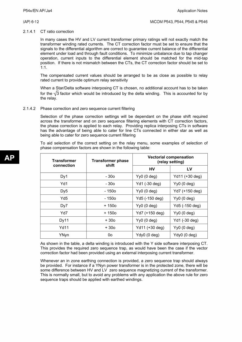
2.1.4.2 Phase correction and zero sequence current filtering
Selection of the phase correction settings will be dependant on the phase shift required across the transformer and on zero sequence filtering elements with CT correction factors, the phase correction is applied to each relay. Providing replica interposing CTs in software has the advantage of being able to cater for line CTs connected in either star as well as being able to cater for zero sequence current filtering
To aid selection of the correct setting on the relay menu, some examples of selection of phase compensation factors are shown in the following table:
Vectorial compensation (relay setting) Transformer
connection Transformer phase
shift HV LV
Dy1 - 30o Yy0 (0 deg) Yd11 (+30 deg)
Yd1 - 30o Yd1 (-30 deg) Yy0 (0 deg)
Dy5 - 150o Yy0 (0 deg) Yd7 (+150 deg)
Yd5 - 150o Yd5 (-150 deg) Yy0 (0 deg)
Dy7 + 150o Yy0 (0 deg) Yd5 (-150 deg)
Yd7 + 150o Yd7 (+150 deg) Yy0 (0 deg)
Dy11 + 30o Yy0 (0 deg) Yd1 (-30 deg)
Yd11 + 30o Yd11 (+30 deg) Yy0 (0 deg)
YNyn 0o Ydy0 (0 deg) Ydy0 (0 deg)
As shown in the table, a delta winding is introduced with the Y side software interposing CT. This provides the required zero sequence trap, as would have been the case if the vector correction factor had been provided using an external interposing current transformer.
Whenever an in zone earthing connection is provided, a zero sequence trap should always be provided. For instance if a YNyn power transformer is in the protected zone, there will be some difference between HV and LV zero sequence magnetizing current of the transformer. This is normally small, but to avoid any problems with any application the above rule for zero sequence traps should be applied with earthed windings.

Application Notes P54x/EN AP/Ja4 MiCOM P543, P544, P545 & P546
(AP) 6-13
2.1.4.3 High set differential setting
When inrush restrain is enabled, a high set differential protection becomes active. This is provided to ensure rapid clearance for heavy internal faults with saturated CTs. Because high set is not restrained by magnetizing inrush, hence the setting must be set such that it will not operate for the largest inrush currents expected. It is difficult to accurately predict the maximum anticipated level of inrush current. Typical waveforms peak values are of the order of 8-10x rated current. A worst case estimation of inrush could me made by dividing the transformer full load current by the per unit leakage reactance quoted by the transformer manufacturer.
2.1.5 Mesh corner and 1½ breaker switched substations
Where a line is fed from a mesh corner or 1½ breaker switched substation, as shown in Figure 1, then two options are available for CT connections to the relay. The first is by paralleling the two sets of line CTs into a common input, ‘A’. The second is by using two separate inputs for each set of line CTs, ‘B’. The P544 and P546 relays are designed with an additional set of input CTs specifically for this purpose.
In the case of a through fault as shown, the relay connected to circuit ‘A’ should see no current and as such, will remain stable. Under this condition, it should be noted that no bias is produced in the relay. To ensure relay stability, the two sets of line CTs should be as near as identical in all characteristics, and equally loaded, such that the relaying connection is at the equipotential point of the secondary leads.
In the case of circuit ‘B’ no differential current should result. A large bias current will however exist, providing a high degree of stability in the event of a through fault. This bias will also ensure stability where CTs are not closely matched. Therefore, circuit ‘B’ is the preferred connection for such applications and so the P544 and P546 relay models would normally be specified.
AP
� �
�
�� ��
�� ������ ���
��������
��������
��������
Figure 1 Breaker and a half switched substation
2.1.6 Small tapped loads (tee feeds)
Where transformer loads are tapped off the protected line it is not always necessary to install CTs at this location. Provided that the tee-off load is light, differential protection can be configured for the main line alone. The settings ‘Phase Char’, ‘Phase Time Delay’ and ‘TMS’ or ‘Time Dial’ in table 3 allow the differential element to time grade with IDMT overcurrent relays or fuses protecting the tap. This keeps stability of the differential protection for external faults on the tee circuit.

P54x/EN AP/Ja4 Application Notes (AP) 6-14
MiCOM P543, P544, P545 & P546
2.2 Optional distance protection
The MiCOM P54x has, by ordering option, a comprehensive integrated distance protection package. This comprises :-
• Phase fault distance protection
• Earth/ground fault distance protection
• Power sing detection, alarm, and blocking
• Out-of-step detection and tripping
• Switch on to fault (SOTF) and trip on reclose (TOR)
• Directional Schemes
• Aided schemes
These are described in the following sections and are marked as being applicable to the distance option only. If the distance option is not specified, these will not be applicable, and additional protection will be in the form of overcurrent etc., as described from section 2.6.
2.3 Distance protection and aided DEF (Distance option only)
2.3.1 Simple and advanced setting mode (Distance option only)
To the benefit of user, the MiCOM P54x offers two setting modes for distance protection: “Simple” and “Advanced”. In the majority of cases, “Simple” setting is recommended, and allows the user merely to enter the line parameters such as length, impedances and residual compensation. Then, instead of entering distance zone impedance reaches in ohms, zone settings are entered in terms of percentage of the protected line. This makes the relay particularly suited to use along with any installed LFZP Optimho relays, as the reduced number of settings mimics the Autocalc facility within Opticom software.
AP
The “Advanced” setting mode is recommended for the networks where the protected and adjacent lines are of dissimilar construction, requiring independent zone characteristic angles and residual compensation. In this setting mode all individual distance ohmic reach and residual compensation settings and operating current thresholds per each zone are accessible. This makes the relay adaptable to any specific application.
2.3.2 Line parameters settings (Distance option only)
It is essential (especially when using the “simple” setting mode) that the data relating to 100% of the protected line is entered here. Take care to input the Line Impedance that correctly corresponds to either Primary or Secondary, whichever has been chosen as the basis for Settings Values in the Configuration column.
2.3.3 Residual compensation for earth/ground faults (Distance option only)
For earth faults, residual current (derived as the vector sum of phase current inputs (Ia + Ib + Ic) is assumed to flow in the residual path of the earth loop circuit. Therefore, the earth loop reach of any zone must generally be extended by a multiplication factor of (1 + kZN) compared to the positive sequence reach for the corresponding phase fault element.
Caution: The kZN Angle is different than previous LFZP, SHNB, and LFZR relays: When importing settings from these older products, subtract. angle ∠ Z1.
2.3.4 Mutual compensation for parallel lines (Distance option only)
Typically a mutual cut off factor of 1.5 is chosen to give a good margin of safety between the requirements of correct mutual compensation for faults inside the protected line and eliminating misoperations for faults on the adjacent line.
Application Notes P54x/EN AP/Ja4-S MiCOM P543, P544, P545 & P546
(AP) 6-15
AP
2.3.5 Selection of distance operating characteristic (Distance option only)
In general, the following characteristics are recommended: Short line applications: Mho phase fault and quadrilateral earth fault zones.
Open delta (vee-connected) VT applications: Mho phase fault, with earth fault distance disabled, and directional earth fault only used for earth fault protection.
Series compensated lines: Recommend always to use mho characteristics for both phase and earth faults.
2.3.5.1 Phase characteristic (Distance option only)
This phase characteristic selection is common to all zones, allowing mho or quadrilateral selection. Generally, the characteristic chosen will match the utility practice. If applied for line protection similarly to LFZP Optimho, LFZR, SHNB Micromho or SHPM Quadramho models in the Schneider Electric range, a mho selection is recommended. For cable applications, or to set similarly to the MiCOM P441/442/444 models, a quadrilateral selection is recommended.
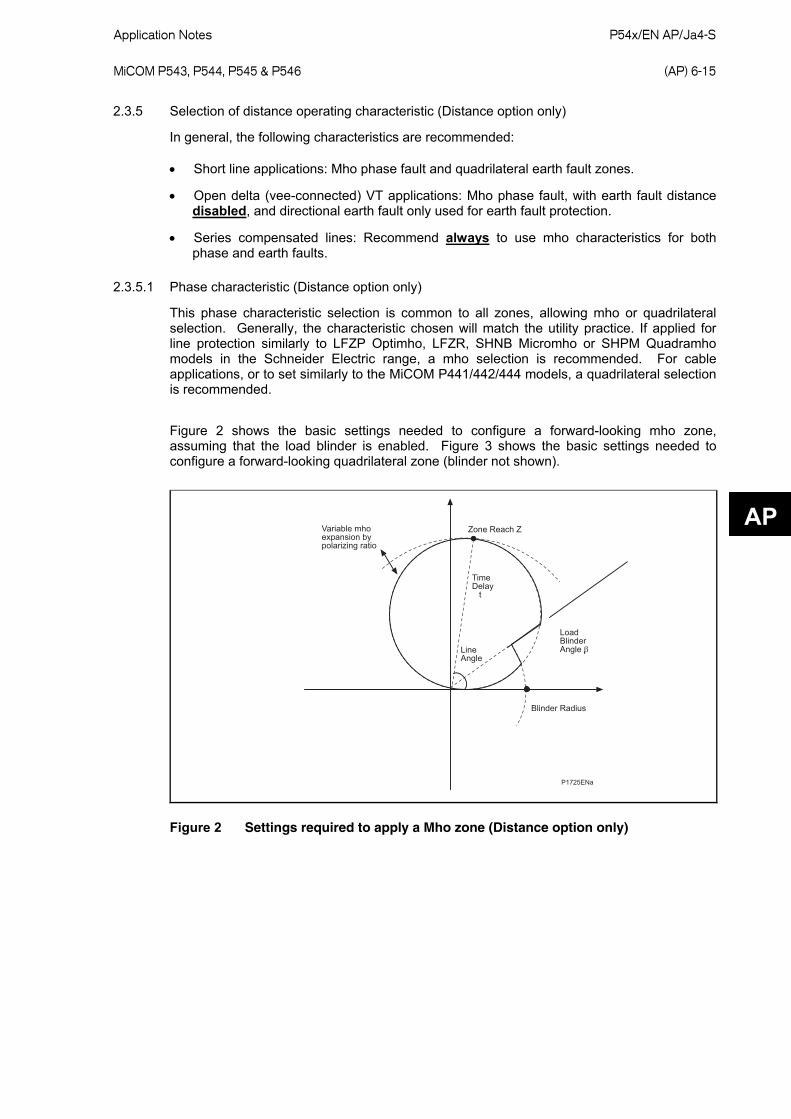
Figure 2 shows the basic settings needed to configure a forward-looking mho zone, assuming that the load blinder is enabled. Figure 3 shows the basic settings needed to configure a forward-looking quadrilateral zone (blinder not shown).
��������
�����������
�� �!��� ��
���������� ���
���������������������������� ������
�����������
��� �
Figure 2 Settings required to apply a Mho zone (Distance option only)

P54x/EN AP/Ja4-S Application Notes (AP) 6-16
MiCOM P543, P544, P545 & P546
AP
����"���
������������
�����������
�����������������
������ �
��� �
Figure 3 Settings required to apply a quadrilateral zone (Distance option only)
2.3.5.2 Ground characteristic (Distance option only)
In general, the same setting philosophy would be followed for ground distance protection as is used for the phase elements. This selection is common to all zones, allowing mho or quadrilateral selection and generally, the characteristic chosen will match the utility practice. If applied for long and medium length line protection similarly to LFZP Optimho, LFZR, SHNB Micromho or SHPM Quadramho models in the Schneider Electric range, a mho selection is recommended. For cable applications, or to set similarly to the MiCOM P441/442/444 models, a quadrilateral selection is recommended.
Quadrilateral ground characteristics are also recommended for all lines shorter than 10 miles (16 km). This is to ensure that the resistive fault arc coverage is not dependent on mho circle dynamic expansion, but will be a known set value.
2.3.6 Zone reaches - recommended settings (Distance option only)
The Zone 1 elements of a distance relay should be set to cover as much of the protected line as possible, allowing instantaneous tripping for as many faults as possible. In most applications the zone 1 reach (Z1) should not be able to respond to faults beyond the protected line. For an underreaching application the zone 1 reach must therefore be set to account for any possible overreaching errors. These errors come from the relay, the VTs and CTs and inaccurate line impedance data. It is therefore recommended that the reach of the zone 1 distance elements is restricted to 80% of the protected line impedance (positive phase sequence line impedance), with zone 2 elements set to cover the final 20% of the line.
The Zone 2 elements should be set to cover the 20% of the line not covered by zone 1. Allowing for underreaching errors, the zone 2 reach (Z2) should be set in excess of 120% of the protected line impedance for all fault conditions. Where aided tripping schemes are used; fast operation of the zone 2 elements is required. It is therefore beneficial to set zone 2 to reach as far as possible, such that faults on the protected line are well within reach. A constraining requirement is that, where possible, zone 2 does not reach beyond the zone 1 reach of adjacent line protection. For this reason the zone 2 reach should be set to cover 50% of the shortest adjacent line impedance, if possible.
The Zone 3 elements would usually be used to provide overall back-up protection for adjacent circuits. The zone 3 reach (Z3) is therefore set to approximately 120% of the combined impedance of the protected line plus the longest adjacent line. A higher apparent impedance of the adjacent line may need to be allowed where fault current can be fed from multiple sources or flow via parallel paths.

Application Notes P54x/EN AP/Ja4 MiCOM P543, P544, P545 & P546
(AP) 6-17
AP
Zone 3 may also be programmed with a slight reverse (“rev”) offset, in which case its reach in the reverse direction is set as a percentage of the protected line impedance too. This would typically provide back-up protection for the local busbar, where the offset reach is set to 20% for short lines (<30 km) or 10% for longer lines.
Zone P is a reversible directional zone. The setting chosen for Zone P, if used at all, will depend upon its application. Typical applications include its use as an additional time delayed zone or as a reverse back-up protection zone for busbars and transformers. Use of zone P as an additional forward zone of protection may be required by some users to line up with any existing practice of using more than three forward zones of distance protection.
The Zone 4 elements may also provide back-up protection for the local busbar. Where zone 4 is used to provide reverse directional decisions for Blocking or Permissive Overreach schemes, zone 4 must reach further behind the relay than zone 2 for the remote end relay. In such cases the reverse reach should be as below (depends on characteristic used):
Mho: Z4 ≥ ((Remote zone 2 reach) x 120%)
Quadrilateral: Z4 ≥ ((Remote zone 2 reach) x 120%) minus the protected line impedance
Note: In the case of the mho, the line impedance is not subtracted. This ensures that whatever the amount of dynamic expansion of the circle, the reverse looking zone will always detect all solid and resistive faults capable of detection by zone 2 at the remote line end.
2.3.7 Quadrilateral phase resistive reaches (Distance option only)
Two setting modes are possible for resistive reach coverage:
Common - In this mode, all zones share one common fault resistive reach setting
Proportional - With this mode, the aspect ratio of (zone reach): (resistive reach) is the same for all zones. The “Fault Resistance” defines a reference fault at the remote end of the line, and depending on the zone reach percentage setting, the resistive reach will be at that same percentage of the Fault Resistance set. For example, if the zone 1 reach is 80% of the protected line, its resistive reach will be 80% of the reference “Fault Resistance”.
Proportional setting is used to mimic Germanic protection practice, and to avoid zones being excessively broad (large resistive reach width compared to zone reach length). In general, for easiest injection testing, the aspect ratio of any zone is best within the 1 : 15 range:
1/15th ≤ Z reach / R reach setting ≤ 15
The resistive reach settings (RPh and RG) should be selected according to the utility practice. If no such guidance exists, a starting point for Zone 1 is:
Cables - Choose Resistive Reach = 3 x Zone 1 reach
Overhead lines - Choose Resistive Reach according to the following formula…
Resistive reach = [2.3 - 0.0045 x Line length (km)] x Zone 1 reach
Lines longer than 400 km - Choose: 0.5 x Zone 1 reach

P54x/EN AP/Ja4 Application Notes (AP) 6-18
MiCOM P543, P544, P545 & P546
2.3.8 Quadrilateral ground resistive reaches and tilting (Distance option only)
Note: Because the fault current for a ground fault may be limited by tower footing resistance, high soil resistivity, and weak infeeding; any arcing resistance is often higher than for a corresponding phase fault at the same location. It maybe necessary to set the RG ground resistive settings to be higher than the RPh phase setting (i.e. boosted higher than the rule of thumb in the last subsection). A setting of RG three times that of RPh is not uncommon.
The P54x allows two different methods of tilting the top reactance line:
• Automatic adjustment of the top reactance line angle
• Fix setting of the top line that will over-ride dynamic tilting
Both methods are detailed in the Operation chapter.
Dynamic tilting:
Medium/ Long lines:
In the case of medium and long line applications where Quad distance ground characteristic is used, the recommended setting is ‘Dynamic tilt’ enabled at starting tilt angle of -3° (as per default settings). The -3° is set to compensate for possible CT/VT and line data errors.
For high resistive faults during power exporting, the under-reaching zone 1 is only allowed to tilt down by the angle difference between the faulted phase and negative sequence current
(Iph-I2) starting from the –3° set angle. This ensures stability of zone 1 for high resistance faults beyond the zone 1 reach even during heavy load conditions (high load angle between two voltage sources) and sufficient sensitivity for high resistance internal faults. The tilt angle for all other zones (that are by nature over-reaching zones) will remain at -3 deg.
AP
In the case of power importing, zone 1 will remain at –3° whilst all other zones will be allowed to tilt up by the (Iph-I2) angle difference, starting from –3°. This will increase the zone 2 and zone 4 resistive reaches and secure correct operation in POR and blocking type schemes.
Short lines:
For very short lines, typically below 10 Miles (16 km), the ratio of resistive to reactance reach setting (R/X) could easily exceed 10. For such applications the geometrical shape of the Quad characteristic could be such that the top reactance line is close or even crosses the resistive axis as presented in Figure 4
Figure 4 Example of high resistive zone 1 fault that falls outside zone 1 characteristic when the starting tilt angle of -3° is set (over-tilting effect). (Distance option only)

Application Notes P54x/EN AP/Ja4 MiCOM P543, P544, P545 & P546
(AP) 6-19
In the case of high resistance external faults on a short line, particularly under heavy power exporting conditions, zone 1 will remain stable due to dynamic downwards tilting of the top line as explained earlier but the detection of high resistance internal faults especially towards the end of the line needs consideration. In such applications a user has a choice to either detect high resistance faults using highly sensitive Aided DEF or Delta Directional schemes or to clear the fault with distance ground protection. If distance is to operate, it is necessary to eliminate over-tilting for internal faults by reducing the initial -3° tilting angle to zero so that the overall top line tilt will equal to (Iph-I2) angle only.
As per Figure 4, the internal resistive fault will then fall in the zone 1 operating characteristic. However, it should be noted that for short lines the load angle is relatively low when compared to long transmission lines for the same transfer capacity and therefore the top line dynamic tilting may be moderate. Therefore it may be necessary to reduce the zone one reach to guarantee zone 1 stability. This is particularly recommended if distance is operating in an aided scheme. To summarize, for very short lines with large R/X setting ratios, it is recommended to set the initial tilt angle to zero and zone 1 reach to 70-75% of the line impedance.
Note: The above discussion assumes homogenous networks where the angle of the negative sequence current derived at relaying point is very close to the total fault current angle. If the network is non-homogenous, there will be a difference in angle that will cause inaccurate dynamic tilting, hence in such networks either quad with fixed tilt angle or even Mho characteristic should be considered in order to avoid zone 1 over-reach.
Fixed tilt angle: AP As an alternative to Dynamic tilting, a user can set a fixed tilt angle. This is applicable to
applications where the power flow direction is unidirectional.
Exporting end:
To secure stability, the tilt angle of zone 1 at exporting end has to be set negative and above the maximum angle difference between sources feeding the resistive faults. This data should be known from load flow study, but if unavailable, the minimum recommended setting would be the angle difference between voltage and current measured at local end during the heaviest load condition coupled with reduced zone 1 reach of 70-75% of the line impedance.
Note: Figure 4 shows that at sharp fixed tilt angle, the effective resistive coverage would be significantly reduced, and therefore for the short lines the dynamic tilting (with variable tilt angle depending on fault resistance and location) is preferred. For all other over-reaching zones set tilting angle to zero.
Importing end:
Set zone 1 tilt angle to zero and for all other zones the typical setting should be positive and between +(5-10)°.
Note: The setting accuracy for over-reaching zones is not crucial because it will not pose a risk for relay’s maloperation, the purpose is only to boost zone 2 and zone 4 reach and improve distance aided schemes.

P54x/EN AP/Ja4 Application Notes (AP) 6-20
MiCOM P543, P544, P545 & P546
AP
2.3.9 Phase fault zone settings (Distance option only)
Each zone has two additional settings that are not accessible in the Simple set mode. These settings are:
• A tilt angle on the top line of any quadrilateral set for phase faults;
• A minimum current sensitivity setting.
By factory defaults, the Top Line of quadrilateral characteristics is not fixed as a horizontal reactance line. To account for phase angle tolerances in the line CT, VT and relay itself, the line is tilted downwards, at a “droop” of –3o. This tilt down helps to prevent zone 1 overreach.
The fixed Tilt setting on the phase elements may also be used to compensate for overreach effects when prefault heavy load export was flowing. In such cases, fault arc resistance will be phase shifted on the impedance polar plot, tilting down towards the resistive axis (i.e. not appearing to be fully resistive in nature). For long lines with heavy power flow, the Zone 1 top line might be tilted downwards within the range –5 to –15o, mimicking the phase shift of the resistance.
Note: A minus angle is used to set a downwards tilt gradient, and a positive angle to tilt upwards.
Note: mho characteristics have an inherent tendency to avoid unwanted overreaching, making them very desirable for long line protection, and one of the reasons for their inclusion within the MiCOM P54x relay.
The current Sensitivity setting for each zone is used to set the minimum current that must be flowing in each of the faulted phases before a trip can occur. It is recommended to leave these settings at their default. The exception is where the relay is made more insensitive to match the lesser sensitivity of older relays existing on the power system, or to grade with the pickup setting of any ground overcurrent protection for tee-off circuits.
2.3.10 Distance directional principle and setup (Distance option only)
2.3.11 Delta directional - selection of RCA (Distance option only)
Distance zones are directionalized by the delta decision. For delta directional decisions, the RCA settings must be based on the average source + line impedance angle for a fault anywhere internal or external to the line. Typically, the Delta Char Angle is set to 60o, as it is not essential for this setting to be precise. When a fault occurs, the delta current will never be close to the characteristic boundary, so an approximate setting is good enough.
The 60° angle is associated with mainly inductive sources and will work perfectly well for most applications. However, in series compensated line applications where the capacitor is physically located behind the line VT the Delta directional characteristic angle needs adjusting. In such applications the capacitor is included in the equivalent source impedance and the overall source impedance as seen by the relay will become predominantly capacitive if the inductance of the source (normally strong source) is less than the capacitor value. In this case, the calculated operating angle during an internal fault may not fall within the default 60° delta directional line operating boundary and that could potentially lead to an incorrect (reverse) directional decision. A zero degree shift will be most suitable for such a fault, but the constraining factor is the case of external faults for which the source is always inductive regardless of the degree of compensation and for which the 60° shift is most appropriate. To ensure correct, reliable and fast operation for both fault locations in case of predominantly capacitive source, a Delta Char Angle setting of 30° is strongly recommended.

Application Notes P54x/EN AP/Ja4 MiCOM P543, P544, P545 & P546
(AP) 6-21
AP
2.3.12 Distance setup - filtering, load blinding and polarizing (Distance option only)
2.3.12.1 Digital filtering (Distance option only)
In most applications, it is recommended that Standard filtering is used. This will ensure that the relay offers fast, sub-cycle tripping. In certain rare cases, such as where lines are immediately adjacent to High Voltage DC (HVDC) transmission, the current and voltage inputs may be severely distorted under fault conditions. The resulting non-fundamental harmonics could affect the reach point accuracy of the relay. To prevent the relay being affected, a ‘Special’ set of filters are available.
Note: When using the long line filter the instantaneous operating time is increased by about a quarter of a power frequency cycle.
2.3.12.2 CVTs with passive suppression of ferroresonance (Distance option only)
Set a Passive CVT filter for any type 2 CVT (those with an anti-resonance design). An SIR cutoff setting needs to be applied, above which the relay operation is deliberately slowed by a quarter of a cycle. A typical setting is SIR = 30, below which the relay will trip sub-cycle, and if the infeed is weak the CVT filter adapts to slow the relay and prevent transient overreach.
2.3.12.3 CVTs with active suppression of ferroresonance (Distance option only)
Set an Active CVT filter for any type 1 CVT.
2.3.13 Load blinding (load avoidance) (Distance option only)
For security, it is highly recommended that the blinder is Enabled, especially for lines above 150 km (90 miles), to prevent non harmonic low frequency transients causing load encroachment problems, and for any networks where power swings might be experienced.
The impedance radius must be set lower than the worst-case loading, and this is often taken as 120% overloading in one line, multiplied by two to account for increased loading during outages or fault clearance in an adjacent parallel circuit. Then an additional allowance for measuring tolerances results in a recommended setting typically 1/3rd (or even 1/4th in some countries such as UK) of the rated full load current:
Z ≤ (Rated phase voltage Vn)/(IFLC x 3)
When the load is at the worst-case power factor, it should remain below the beta setting. So, if we assume a typical worst-case 0.85 power factor, then:
β ≥ Cos-1 (0.85) plus 15o margin ≥ 47o
− And, to ensure that line faults are detected, β ≤ (Line Angle -15o).
In practice, an angle half way between the worst-case leading load angle, and the protected line impedance angle, is often used.
The MiCOM P54x has a facility to allow the load blinder to be bypassed any time the measured voltage for the phase in question falls below an undervoltage V< setting. Under such circumstances, the low voltage could not be explained by normal voltage excursion tolerances on-load. A fault is definitely present on the phase in question, and it is acceptable to override the blinder action and allow the distance zones to trip according to the entire zone shape. The benefit is that the resistive coverage for faults near to the relay location can be higher.
The undervoltage setting must be lower than the lowest phase-neutral voltage under heavy load flow and depressed system voltage conditions. The typical maximum V< setting is 70% Vn.

P54x/EN AP/Ja4 Application Notes (AP) 6-22
MiCOM P543, P544, P545 & P546
AP
2.3.13.1 Recommended polarizing settings (Distance option only)
Cable applications - In line with LFZP123 or LFZR applications for cable feeders, use only minimum 20% (0.2) memory, which results in minimum mho expansion. This keeps the protected line section well within the expanded mho, thereby ensuring better accuracies and faster operating times for close-up faults.
Series compensated lines - Use a mho with maximum memory polarizing (setting = 5). The large memory content will ensure correct operation even with the negative reactance effects of the compensation capacitors seen either within Zs, or within the line impedance.
Short lines - For lines shorter than 10 miles (16 km), or with an SIR higher than 15, use maximum memory polarizing (setting = 5). This ensures sufficient characteristic expansion to cover fault arc resistance.
General line applications - Use any setting between 0.2 and 1.
2.3.14 Distance elements basic scheme setting (Distance option only)
The Zone 1 time delay (tZ1) is generally set to zero, giving instantaneous operation.
The Zone 2 time delay (tZ2) is set to co-ordinate with zone 1 fault clearance time for adjacent lines. The total fault clearance time will consist of the downstream zone 1 operating time plus the associated breaker operating time. Allowance must also be made for the zone 2 elements to reset following clearance of an adjacent line fault and also for a safety margin. A typical minimum zone 2 time delay is of the order of 200 ms.
The Zone 3 time delay (tZ3) is typically set with the same considerations made for the zone 2 time delay, except that the delay needs to co-ordinate with the downstream zone 2 fault clearance. A typical minimum zone 3 operating time would be in the region of 400 ms.
The Zone 4 time delay (tZ4) needs to co-ordinate with any protection for adjacent lines in the relay’s reverse direction.
Note (1): The MiCOM P54x allows separate time delays to be applied to both phase and ground fault zones, for example where ground fault delays are set longer to time grade with external ground/earth overcurrent protection.
Note (2): Any zone (“#”) which may reach through a power transformer reactance, and measure secondary side faults within that impedance zone should have a small time delay applied. This is to avoid tripping on the inrush current when energizing the transformer. As a general rule, if: Z# Reach setting > 50% XT transformer reactance, set: tZ# ≥ 100 ms. Alternatively, the 2nd harmonic detector that is available in the Programmable Scheme Logic may be used to block zones that may be at risk of tripping on inrush current. Settings for the inrush detector are found in the SUPERVISION menu column.

Application Notes P54x/EN AP/Ja4 MiCOM P543, P544, P545 & P546
(AP) 6-23
Figure 5 shows the typical application of the Basic scheme.
#$����������������
� �
�
�����
���������%
�����
���������%
#��
#��
#�%
#�&
��
��
��
�%
�&
����$��
�#!����
#��
#��
#�%
#�&
��
��
��
�%
�&
����$�
�#!���
����'�������(�! ������� ���� �������
#�� #��
���&&��� AP
Figure 5 Basic time stepped distance scheme (Distance option only)
2.3.15 Power swing alarming and blocking (Distance option only)
The PSB technique employed in the MiCOM P54x has the significant advantage that it is adaptive and requires no user-set thresholds in order to detect swings faster than 0.5 Hz. The PSB relies on the delta techniques internal to the relay, which automatically detect swings. During the power oscillations slower than 0.5 Hz the continuous ∆I phase current integral to the detection technique for swing conditions may fall below the sensitive threshold of ∆I=0.05 In therefore may not operate. These slow swings will usually occur following sudden load changes or single pole tripping on the weaker systems where the displacement of initial power transfer is not severe. The slow swings of up to 1 Hz are by its nature recoverable swings but the swing impedance may stay longer inside the distance characteristics until the oscillations are damped by the power system. Therefore, to guarantee system stability during very slow swings it is recommended to set a blinder to complement the automatic, setting free detection algorithm. Zone 5 is used as a blinder for slow swing detection as well as for the Out of Step (OST) protection described in the next section. Zone 5 settings are therefore visible even if OST protection is disabled. The slow swing condition will be declared if positive sequence impedance is detected inside zone 5 for more than a cycle without phase selection operation. The slow swing detection operates in parallel to automatic swing detection mechanism.
No system calculation is needed for zone 5 setting, it is only important to set zone 5 smaller than the minimum possible load impedance with a security margin:
P54x/EN AP/Ja4 Application Notes (AP) 6-24
MiCOM P543, P544, P545 & P546
AP
In case the OST is enabled the R5, R5’, Z5 and Z5’ settings will be adequate for very slow swing detection. If, however, the OST protection is disabled, set:
R5=R5’=0.85 x Z<
Z5=Z5’=2 x Zline
where Z< is load blinder radius determined in the 2.3.13 Section.
The user decides which zones are required to be blocked.
Two timers are available:
The PSB Reset Delay is used to maintain the PSB status when ΔI naturally is low during the swing cycle (near the current maxima and minima in the swing envelope). A typical setting of 0.2 s is used to seal-in the detection until ΔI has chance to appear again.
The PSB Unblock Dly is used to time the duration for which the swing is present. The intention is to allow the distinction between a stable and an unstable swing. If after the timeout period the swing has still not stabilized, the block for selected zones can be released (“unblocking”), giving the opportunity to split the system. If no unblocking is required at the location of this relay, set to maximum (10 s).
PSB can be disabled on distribution systems, where power swings would not normally be experienced.
2.3.16 Out of step protection (Distance option only)
P54x provides an integrated Out of Step protection, therefore avoiding a need for a separate stand alone Out of Step relays. Unlike the power swing detection, the Out of Step protection requires settings and is completely independent from the setting free Power swing detection.
This section provides a discussion and a guidance of how to set the Out of Step protection.
Settings based on system studies must be applied when ‘Predictive OST’ operation mode is selected as the high setting accuracy is needed to avoid premature system splitting in the case of severe power oscillations that do not lead to pole slip conditions. For the ‘OST’ setting the same method may be used but an exhaustive stability study may not be required as it will be shown later that the total system impedance ZT and system split points are adequate to set the relay for this scenario.
The MiCOM P54x Out of Step protection can operate as a stand alone protection, i.e. Distance protection may be completely disabled under Configuration column.
2.3.17 Critical stability angle (Distance option only)
What is the angle between two ends when a power system oscillation could be declared as a pole slip?
Consider the power angle curves as in Figure 6.
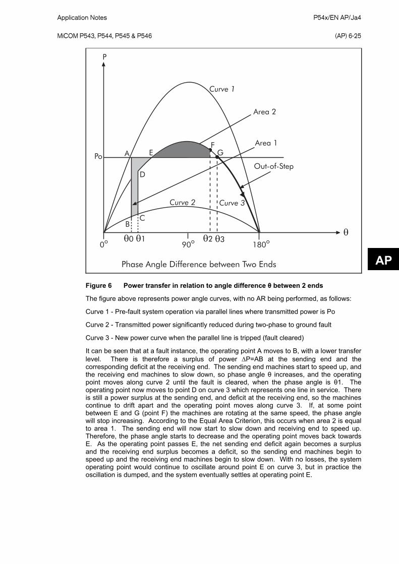
Application Notes P54x/EN AP/Ja4 MiCOM P543, P544, P545 & P546
(AP) 6-25
�� �� ��
������ �������������������
�
�� �
�������������
��
��
�
�
����
����
�
� �!��!"�#
$���� �%��
������
�&
AP
Figure 6 Power transfer in relation to angle difference θ between 2 ends
The figure above represents power angle curves, with no AR being performed, as follows:
Curve 1 - Pre-fault system operation via parallel lines where transmitted power is Po
Curve 2 - Transmitted power significantly reduced during two-phase to ground fault
Curve 3 - New power curve when the parallel line is tripped (fault cleared)
It can be seen that at a fault instance, the operating point A moves to B, with a lower transfer level. There is therefore a surplus of power ΔP=AB at the sending end and the corresponding deficit at the receiving end. The sending end machines start to speed up, and the receiving end machines to slow down, so phase angle θ increases, and the operating point moves along curve 2 until the fault is cleared, when the phase angle is θ1. The operating point now moves to point D on curve 3 which represents one line in service. There is still a power surplus at the sending end, and deficit at the receiving end, so the machines continue to drift apart and the operating point moves along curve 3. If, at some point between E and G (point F) the machines are rotating at the same speed, the phase angle will stop increasing. According to the Equal Area Criterion, this occurs when area 2 is equal to area 1. The sending end will now start to slow down and receiving end to speed up. Therefore, the phase angle starts to decrease and the operating point moves back towards E. As the operating point passes E, the net sending end deficit again becomes a surplus and the receiving end surplus becomes a deficit, so the sending end machines begin to speed up and the receiving end machines begin to slow down. With no losses, the system operating point would continue to oscillate around point E on curve 3, but in practice the oscillation is dumped, and the system eventually settles at operating point E.

P54x/EN AP/Ja4 Application Notes (AP) 6-26
MiCOM P543, P544, P545 & P546
AP
1.
2.
3. OST
4.
To resume, if area 1<area 2, the system will stay in synchronism. This swing is usually called a recoverable power swing. If, on contrary, the system passes point G with a further increase in angle difference between sending and receiving ends, the system drifts out of synchronism and becomes unstable. This will happen if the initial power transfer Po was set too high in Figure 6, so that the area 1 is greater than area 2. This power swing is not recoverable and is usually called out of step or out of synchronism or pole slip condition. After this, only system separation and re-synchronizing of the machines can restore normal system operation.
In Figure 6, the point G is shown at approximately 120° deg, but it is not true in all cases. If, for example the pre-fault transmitted power (Po) was too high and if the fault clearance was slow, the area 1 will be greater so for the system to recover the angle θ would be close to 90 deg. On contrarily, if the pre-fault transmitted power Po was low and fault clearance fast, the area 1 will be small, so that based on area comparison, the angle θ could go closer to 180 deg and the system will still remain stable.
The actual angle difference at which system will become unstable could only be determined by a particular system studies, but for the purpose of settings recommendation where ‘OST’ setting is selected, the typical angle beyond which system will not recover is assumed to be 120 deg.
2.3.17.1 Setting option recommendation (Distance option only)
The relay provides 4 different setting options:
Disabled
Predictive OST
Predictive OST or OST
Set Option 1 on all lines except the line where tripping due to unrecoverable power oscillations is required or for the system where power oscillations are not severe - mainly in well interconnected systems operating with 3 phase tripping.
Setting Option 2 (and 4) is the best setting option from the system point of view, perhaps not being widely used in the past. Some utilities prefer an early system split to minimize the angle shift between ends and maximize the chances for the remaining two halves to stabilize as quickly as possible. Special care must be taken when this method is applied to ensure that the actual circuit breaker opening does not occur when the internal voltages at two ends are in anti phase. This is due to the fact that most breakers are not designed to interrupt at double nominal voltage and any attempt to break at that point would lead to flash over and possible circuit breaker damage. The fact is that setting Option 2 (and 4) will be mainly applied do detect and trip fast power oscillations. When this is coupled with a typical 2 cycle circuit breaker operating time, the two voltages angles may rapidly move in opposite directions at the time of opening the circuit breaker. Therefore, if this setting option is chosen, the above facts must be taken into account so that the actual CB opening must occur well before the angle difference between two ends approaches 180 degrees. On that basis, accurate settings have to be determined based on exhaustive system studies.
Setting Option 3 is the most commonly used approach. Once the Out of Step conditions are detected, the OST command will split the system at pre-determined points. The slight disadvantages of this method in comparison to Option 2 (and 4) is that the power oscillation will escalate further, thus causing more difficulties for the split parts to remain stable but the advantage is that the timing of the circuit breaker operation (‘tripping angle’) is easily controlled and the decision to split the system will be correct even if errors were made in the system data and setting parameters. This extra security is achieved by measuring and confirming the change of polarity of the resistive part of positive sequence impedance on zone 5 exit (reset).
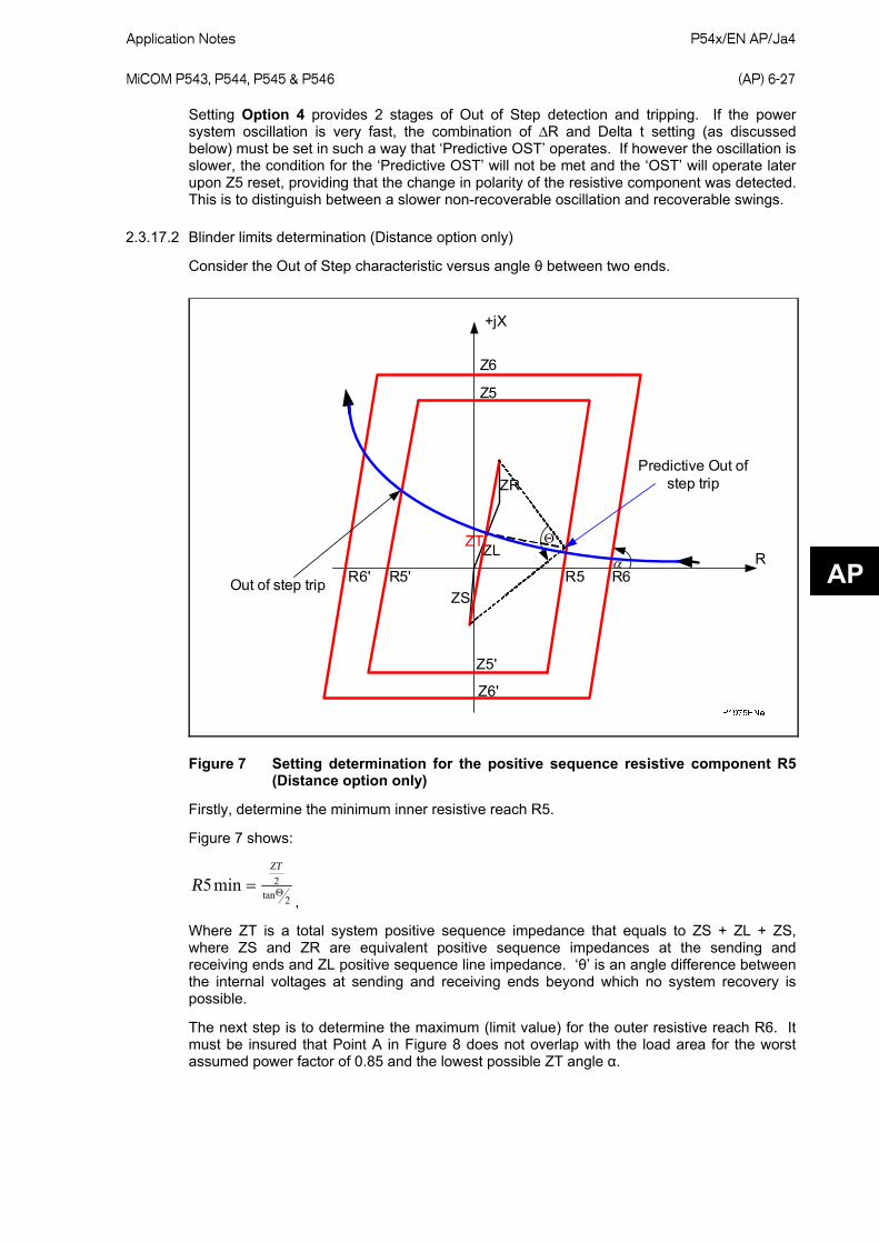
Application Notes P54x/EN AP/Ja4 MiCOM P543, P544, P545 & P546
(AP) 6-27
Setting Option 4 provides 2 stages of Out of Step detection and tripping. If the power system oscillation is very fast, the combination of ∆R and Delta t setting (as discussed below) must be set in such a way that ‘Predictive OST’ operates. If however the oscillation is slower, the condition for the ‘Predictive OST’ will not be met and the ‘OST’ will operate later upon Z5 reset, providing that the change in polarity of the resistive component was detected. This is to distinguish between a slower non-recoverable oscillation and recoverable swings.
2.3.17.2 Blinder limits determination (Distance option only)
Consider the Out of Step characteristic versus angle θ between two ends.
Out of step trip
R
Z5
+jX
AP ZL
Z6
Z5'
Z6'
R5 R6R5'R6'
Predictive Out of step trip
α
ZR
ZS
ΘZT
Figure 7 Setting determination for the positive sequence resistive component R5 (Distance option only)
Firstly, determine the minimum inner resistive reach R5.
Figure 7 shows:
2tan2min5 Θ=
ZT
R,
Where ZT is a total system positive sequence impedance that equals to ZS + ZL + ZS, where ZS and ZR are equivalent positive sequence impedances at the sending and receiving ends and ZL positive sequence line impedance. ‘θ’ is an angle difference between the internal voltages at sending and receiving ends beyond which no system recovery is possible.
The next step is to determine the maximum (limit value) for the outer resistive reach R6. It must be insured that Point A in Figure 8 does not overlap with the load area for the worst assumed power factor of 0.85 and the lowest possible ZT angle α.
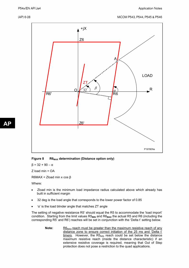
P54x/EN AP/Ja4 Application Notes (AP) 6-28
MiCOM P543, P544, P545 & P546
R
Z6
Z6'
R6R6'α
+jX
AP
ZT
A
LOAD
β°32O
P1976ENa
Figure 8 R6MAX determination (Distance option only)
β = 32 + 90 – α
Z load min = OA
R6MAX < Zload min x cos β
Where:
• Zload min is the minimum load impedance radius calculated above which already has built in sufficient margin
• 32 deg is the load angle that corresponds to the lower power factor of 0.85
• ‘α’ is the load blinder angle that matches ZT angle
The setting of negative resistance R5’ should equal the R5 to accommodate the ‘load import’ condition. Starting from the limit values R5MIN and R6MAX the actual R5 and R6 (including the corresponding R5’ and R6’) reaches will be set in conjunction with the ‘Delta t’ setting below.
Note: R6MAX reach must be greater than the maximum resistive reach of any distance zone to ensure correct initiation of the 25 ms and ‘Delta t’ timers. However, the R5MIN reach could be set below the distance maximum resistive reach (inside the distance characteristic) if an extensive resistive coverage is required, meaning that Out of Step protection does not pose a restriction to the quad applications.
Application Notes P54x/EN AP/Ja4 MiCOM P543, P544, P545 & P546
(AP) 6-29
AP
Setting of reactance lines Z5 and Z6 will depend on how far from the relay location the power oscillations are to be detected. Normally, there is only one point where the system is to be initially split and that point will be determined by system studies. For that reason, the Out of Step protection must be enabled at that location and disabled on all others. To detect the Out of step conditions, the Z5’-Z5 and Z6’-Z6 setting must be set to comfortably encompass the total system impedance ZT, as shown in Figure 7. Typical setting could be:
Z5 = Z5’ = 1/2 x 2 ZT = ZT
The Z6 and Z6’ setting is not of great importance and could be set to Z6 = Z6’ = 1.1 x Z5
2.3.17.3 Delta t, R5 and R6 setting determination (Distance option only)
The R5MIN and R6MAX settings determined above are only limit values, the actual R5 and R6 need to be determine in relation to the ‘Delta t’ timer.
Predictive OST setting:
For the ‘Predictive OST’ setting it is important to:
• Set R6 (and R6’) equal to R6MAX
• Set R5 as close as practical to R6MAX
The aim of pushing the R5 setting to the right is to detect the fast oscillation as soon as possible to gain sufficient time to operate the breaker before the two source voltages are in opposite direction. The only restriction would be the limitation of the ‘Delta t’ minimum time delay of 30 ms and the speed of oscillation. Set ‘Delta t’ so that the following condition is satisfied:
‘Delta t’ does not expire after positive sequence impedance has passed the R6-R5 region
For this setting, knowledge of the accurate rate of change of swing impedance when crossing the R6-R5 region is essential and therefore must be based on system studies.
Assumption that the rate of change of the positive sequence impedance during crossing the R6-R5 region is average rate of change for the whole swing cycle is wrong and could easily lead to incorrect ‘Predictive OST’ operation.
Note: For the fault, the R6-R5 region will be passed faster than 25 ms, therefore even very fast oscillations of 7 Hz will not be mistaken with the fault condition and ‘Predictive OST’ will not operate.
OST setting:
For the ‘OST’ setting option the precise setting of blinders and ‘Delta t’ is not necessary. This is based on the fact that:
The wider the ∆R region and the shorter the ∆t setting, any oscillation will be successfully detected. The only condition is that the fault impedance must pass through the ∆R region faster than ∆t setting.
Therefore, for the ‘OST’ setting assume that θ = 120° and set:
• R5 = R5’ = R5MIN = ZT/3.46
• R6 = R6’ = R6MAX
• Delta t = 30 ms
The point is that ‘Delta t’ always expires, therefore the above setting will secure the detection of a wide range of oscillations, starting from very slow oscillations caused by recoverable swings up to the fastest oscillation of 7 Hz. It should be noted that any fault impedance will pass the R6-R5 region faster than the minimum settable ‘Delta t’ time of 30 ms.
Predictive OST or OST setting:
As per ‘Predictive OST’ above.

P54x/EN AP/Ja4 Application Notes (AP) 6-30
MiCOM P543, P544, P545 & P546
AP
2.3.17.4 Tost (trip delay) setting (Distance option only)
Tost must be set zero for setting Option 2 and 4 above.
For setting Option 3, Tost should normally be set to zero. It is only the case if a user wants to operate breaker at the angle closer to 360 degrees (when voltages are in phase) when time delay could be applied.
2.3.17.5 Blinder angle setting (Distance option only)
Set blinders angle ‘α’ same as total system impedance ZT angle.
2.3.17.6 Out of step operation on series compensated lines (Distance option only)
The maximum phase currents during out of step condition rarely exceed 2xIn RMS, which corresponds to the minimum swing impedance passing through zone 1. Since the Metal-Oxide Varistors (MOV) bypass level is normally set between 2-3In, they will not operate during the power oscillations and therefore in majority of applications will not make any impact on Out of Step operation.
Consider a worst case scenario when the power oscillations are triggered upon fault clearance on the parallel line. In that case approximately twice the load current will start flowing through the remaining circuit, increase further and eventually exceed the MOV threshold. Since the R6-R5 region is usually set far from zone 1 the chances that the positive sequence impedance’s trajectory may traverse in and out of the set ∆R region due to MOV’s operation, are remote. If MOV’s do operate within the ∆R region (see Figure 9), a timer, that has been initiated, may reset and be re-initiated or the impedance may remain within ∆R region for a slightly longer duration. This is due to the fact that resistive and capacitive components will be added to the measured impedance during MOV operation as per Figure 9. This effect may have an impact on the ‘Delta t’ measurement if ‘Predictive OST’ setting is used. If the recommendation to set R5MIN as close as practically possible to the R6MAX is followed, the chances that the swing currents will exceed MOV threshold within the ∆R region is very remote. If a study shows that the MOV’s could operate within the ∆R region, it is recommended to set ‘Predictive OST and OST’ operating mode to cover all eventualities.

Application Notes P54x/EN AP/Ja4 MiCOM P543, P544, P545 & P546
(AP) 6-31
R
Z5
ZL
Z6
Z5'Z6'
R5 R6R5'R6'
+jX
MOV’s operation
∆R
AP
Figure 9 Example of timer reset due to MOV’s operation
Note: If ‘OST’ setting is chosen, the timer when triggered, will eventually expire as the power oscillations progress, therefore MOV operation will not have any impact on Out of Step operation.
2.3.18 Switch on to fault (SOTF) and trip on reclose (TOR) (Distance option only)
2.3.19 Switch onto fault mode (Distance option only)
To ensure fast isolation of faults (for example a closed three phase earth/grounding switch) upon energization, it is recommended this feature is enabled with appropriate zones and/or ‘Current No Volt’ (CNV) level detectors, depend on utility practices.
When busbar VTs are used, ‘Pole Dead’ signal will not be produced and a user has to connect circuit breaker auxiliary contacts for correct operation. This is not necessary if the SOTF is activated by an external pulse.
SOTF delay - The time chosen should be longer than the slowest delayed- auto-reclose dead time, but shorter than the time in which the system operator might re-energize a circuit once it had opened/tripped. 110 seconds is recommended as a typical setting.
SOTF pulse - Typically this could be set to at 500 ms. This time is enough to establish completely the voltage memory of distance protection.
TOC reset delay - 500 ms is recommended as a typical setting (chosen to be in excess of the 16 cycles length of memory polarizing, allowing full memory charging before normal protection resumes).
P54x/EN AP/Ja4 Application Notes (AP) 6-32
MiCOM P543, P544, P545 & P546
AP
2.3.20 Trip on reclose mode (Distance option only)
To ensure fast isolation of all persistent faults following the circuit breaker reclosure. It is recommended this feature is enabled with appropriate zones selected and/or ‘Current No Volt’ (CNV) level detectors.
TOC Delay the TOR is activated after ‘TOC Delay’ has expired. The setting must not exceed the minimum AR Dead Time setting to make sure that the TOR is active immediately upon reclose command.
TOC reset delay - 500 ms is recommended as a typical setting (as per SOTF).
2.3.21 Setup of DEF (Distance option only)
DEF zero sequence polarization
In practice, the typical zero sequence voltage on a healthy system can be as high as 1% (i.e.: 3% residual), and the VT error could be 1% per phase. A VNpol Set setting between 1% and 4%.Vn is typical, to avoid spurious detection on standing signals. The residual voltage measurement provided in the Measurements column of the menu may assist in determining the required threshold setting during commissioning, as this will indicate the level of standing residual voltage present. The Virtual Current Polarizing feature will create a VNpol which is always large, regardless of whether actual VN is present.
With DEF, the residual current under fault conditions lies at an angle lagging the polarizing voltage. Hence, negative characteristic angle settings are required for DEF applications. This is set in cell ‘DEF Char Angle' in the relevant earth fault menu.
The following angle settings are recommended for a residual voltage polarized relay:-
Distribution systems (solidly earthed) ⇒ -45°
Transmissions systems (solidly earthed) ⇒ -60°
2.3.22 DEF negative sequence polarization (Distance option only)
For negative sequence polarization, the RCA settings must be based on the angle of the upstream negative phase sequence source impedance. A typical setting is -60o.
2.3.23 General setting guidelines for DEF (directional ground overcurrent) (Distance option only)
DEF forward threshold - This setting determines the current sensitivity (trip sensitivity) of the DEF aided scheme. This setting must be set higher than any standing residual current unbalance. A typical setting will be between 10 and 20% In.
DEF reverse threshold - This setting determines the current sensitivity for the reverse ground fault. The setting must always be below the DEF forward threshold for correct operation of Blocking scheme and to provide stability for current reversal in parallel line applications. The recommended setting is 2/3 of DEF forward setting. Note that this setting has to be above the maximum steady state residual current unbalance.
2.3.24 Delta directional comparison principle and setup (Distance option only)
For delta directional decisions, the RCA settings must be based on the average source + line impedance angle for a fault anywhere internal or external to the line. Typically, the Delta Char Angle is set to 60o, as it is not essential for this setting to be precise. When a fault occurs, the delta current will never be close to the characteristic boundary, so an approximate setting is good enough.
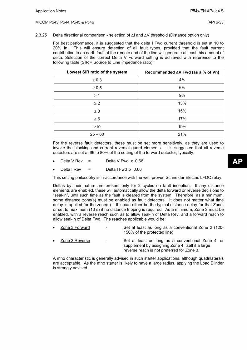
Application Notes P54x/EN AP/Ja4-S MiCOM P543, P544, P545 & P546
(AP) 6-33
AP
2.3.25 Delta directional comparison - selection of I and V threshold (Distance option only)
For best performance, it is suggested that the delta I Fwd current threshold is set at 10 to 20% In. This will ensure detection of all fault types, provided that the fault current contribution to an earth fault at the remote end of the line will generate at least this amount of delta. Selection of the correct Delta V Forward setting is achieved with reference to the following table (SIR = Source to Line impedance ratio):
Lowest SIR ratio of the system Recommended V Fwd (as a % of Vn)
0.3 4%
0.5 6%
1 9%
2 13%
3 15%
5 17%
10 19%
25 – 60 21%
For the reverse fault detectors, these must be set more sensitively, as they are used to invoke the blocking and current reversal guard elements. It is suggested that all reverse detectors are set at 66 to 80% of the setting of the forward detector, typically:
Delta V Rev = Delta V Fwd x 0.66
Delta I Rev = Delta I Fwd x 0.66
This setting philosophy is in-accordance with the well-proven Schneider Electric LFDC relay.
Deltas by their nature are present only for 2 cycles on fault inception. If any distance elements are enabled, these will automatically allow the delta forward or reverse decisions to “seal-in”, until such time as the fault is cleared from the system. Therefore, as a minimum, some distance zone(s) must be enabled as fault detectors. It does not matter what time delay is applied for the zone(s) – this can either be the typical distance delay for that Zone, or set to maximum (10 s) if no distance tripping is required. As a minimum, Zone 3 must be enabled, with a reverse reach such as to allow seal-in of Delta Rev, and a forward reach to allow seal-in of Delta Fwd. The reaches applicable would be:
Zone 3 Forward - Set at least as long as a conventional Zone 2 (120- 150% of the protected line)
Zone 3 Reverse - Set at least as long as a conventional Zone 4, or supplement by assigning Zone 4 itself if a large reverse reach is not preferred for Zone 3.
A mho characteristic is generally advised in such starter applications, although quadrilaterals are acceptable. As the mho starter is likely to have a large radius, applying the Load Blinder is strongly advised.
P54x/EN AP/Ja4 Application Notes (AP) 6-34
MiCOM P543, P544, P545 & P546
AP
2.4 Channel aided schemes (Distance option only)
The MiCOM P54x offers two sets of aided channel (“pilot”) schemes, which may be operated in parallel.
Aided Scheme 1 - May be keyed by distance and/or DEF and/ or delta directional comparison
Aided Scheme 2 - May be keyed by distance and/or DEF and/ or delta directional comparison
When schemes share the same channel, the same generic scheme type will be applied - i.e. ALL Permissive Overreach, or ALL Blocking.
2.4.1 Distance scheme PUR - permissive underreach transfer trip (Distance option only)
This scheme is similar to that used in the LFZP Optimho, SHNB Micromho, LFZR, and MiCOM P44x (note 1) distance relays. (Note 1: matches PUP Z2 mode in P441/442/444). It allows an instantaneous Z2 trip on receipt of the signal from the remote end protection.
Send logic: Zone 1
Permissive trip logic: Zone 2 plus Channel Received
The “Dist dly” trip time setting should be set to Zero, for fast fault clearance.
2.4.2 Distance scheme POR - permissive overreach transfer trip (Distance option only)
This scheme is similar to that used in the LFZP Optimho, SHNB Micromho, LFZR, and MiCOM P44x (note 2) distance relays. (Note 2: matches POP Z2 mode in P441/442/444, and POR2 scheme in LFZP/LFZR). Note that the POR scheme also uses the reverse looking zone 4 of the relay as a reverse fault detector. This is used in the current reversal logic and in the optional weak infeed echo feature.
Send logic: Zone 2
Permissive trip logic: Zone 2 plus Channel Received
The “Dist dly” trip time setting should be set to Zero, for fast fault clearance.
2.4.3 Permissive overreach trip reinforcement (Distance option only)
The send logic in the POR scheme is done in such a way that for any trip command at the local end, the relay sends a channel signal to the remote end(s) in order to maximize the chances for the fault to be isolated at all ends.
Note: The send signal is generated by the ‘Any trip’ command and is sent on both channels, Ch1 and Ch2, if more than one channel is in use. This feature is termed permissive trip reinforcement, and is a deliberate attempt to ensure that synchronous tripping occurs at all line ends.
2.4.4 Permissive overreach scheme weak infeed features (Distance option only)
Where weak infeed tripping is employed, a typical voltage setting is 70% of rated phase-neutral voltage. Weak infeed tripping is time delayed according to the WI Trip Delay value, usually set at 60 ms.

Application Notes P54x/EN AP/Ja4-S MiCOM P543, P544, P545 & P546
(AP) 6-35
AP
2.4.5 Distance scheme BLOCKING (Distance option only)
To allow time for a blocking signal to arrive, a short time delay on aided tripping, “Dist dly”, must be used, as follows:
Recommended Dly setting = Max. Signaling channel operating time + 1 power frequency cycle.
This scheme is similar to that used in the LFZP Optimho, SHNB Micromho, LFZR, and MiCOM P44x (note 3) distance relays. (Note 3: matches BOP Z2 mode in P441/442/444).
Send logic: Reverse Zone 4
Trip logic: Zone 2, plus Channel NOT Received, delayed by Tp
Note: Two variants of a Blocking scheme are provided, Blocking 1 and Blocking 2. Both schemes operate identically, except that the reversal guard timer location in the logic changes. Blocking 2 may sometimes allow faster unblocking when a fault evolves from external to internal, and hence a faster trip.
2.4.6 Permissive overreach schemes current reversal guard (Distance option only)
The recommended setting is:
tREVERSAL GUARD = Maximum signaling channel reset time + 35 ms.
2.4.7 Blocking scheme current reversal guard (Distance option only)
The recommended setting is:
Where Duplex signaling channels are used:
tREVERSAL GUARD = Maximum signaling channel operating time + 20 ms.
Where Simplex signaling channels are used:
tREVERSAL GUARD = Maximum signaling channel operating time - minimum signaling channel reset time + 20 ms.
2.4.8 Aided DEF ground fault scheme - permissive overreach (Distance option only)
This POR scheme is similar to that used in all other Schneider Electric relays.
Send logic: IN> Forward pickup
Permissive trip logic: IN> Forward plus Channel Received
Note: The Time Delay for a permissive scheme aided trip would normally be set to zero.
2.4.9 Aided DEF ground fault scheme - blocking (Distance option only)
This scheme is similar to that used in all other Schneider Electric relays.
Send logic: DEF Reverse
Trip logic: IN> Forward, plus Channel NOT Received, with a small set delay
To allow time for a blocking signal to arrive, a short time delay on aided tripping must be used. The recommended Time Delay setting = max. Signaling channel operating time + 20 ms.
P54x/EN AP/Ja4-S Application Notes (AP) 6-36
MiCOM P543, P544, P545 & P546
AP
2.4.10 Delta scheme POR - permissive overreach transfer trip (Distance option only)
This scheme is similar to that used in the LFDC relay.
Send logic: Fault Forward
Permissive trip logic: Fault Forward plus Channel Received.
The Delta Delay trip time setting should be set to zero, for fast fault clearance.
2.4.11 Delta blocking scheme (Distance option only)
This scheme is similar to that used in the LFDC relay.
Send logic: Fault Reverse
Trip logic: Fault Forward, plus Channel NOT Received, delayed by Tp.
Recommended Dly setting = Max. signaling channel operating time + 6 ms.
2.4.12 Delta schemes current reversal guard timer (Distance option only)
Similarly to the distance protection schemes, current reversals during fault clearance on an adjacent parallel line need to be treated with care. In order to prevent misoperation (mal-tripping) of the protection on the unfaulted line, a current reversal guard timer must be set. The recommended setting for both POR and BLOCKING schemes is:
tREVERSAL GUARD = Maximum signaling channel reset time + 35 ms
2.5 Loss of load accelerated tripping (LoL) (Distance option only)
For circuits with load tapped off the protected line, care must be taken in setting the loss of load feature to ensure that the I< level detector setting is above the tapped load current. When selected, the loss of load feature operates in conjunction with the main distance scheme that is selected. In this way it provides high speed clearance for end zone faults when the Basic scheme is selected or, with permissive signal aided tripping schemes, it provides high speed back-up clearance for end zone faults if the channel fails.
2.6 Phase fault overcurrent protection
Settings for the time delayed overcurrent element should be selected to ensure discrimination with surrounding protection. Setting examples for phase fault overcurrent protection can be found in the Network Protection and Automation Guide (NPAG), a comprehensive reference textbook available from Schneider Electric.
Caution: The IEEE C.37.112 standard for IDMT curves permits some freedom to manufacturers at which time dial (TD) value the reference curve applies. Rather than pick a mid-range value, for the MiCOM P54x the reference curve norm applies at a time dial of 1. The time dial is merely a multiplier on the reference curve, in order to achieve the desired tripping time. Take care when grading with other suppliers' relays which may take TD = 5, or TD = 7 as a mid-range value to define the IDMT curve. The equivalent MiCOM P54x setting to match those relays is achieved by dividing the imported setting by 5 or 7.

Application Notes P54x/EN AP/Ja4 MiCOM P543, P544, P545 & P546
(AP) 6-37
AP
2.6.1 Directional overcurrent characteristic angle settings
The relay uses a 90° connection angle for the directional overcurrent elements. The relay characteristic angles in this case are nominally set to:
• +30° Plain feeders, zero sequence source behind relay
• +45° Transformer feeder, zero sequence source in front of relay
Whilst it is possible to set the RCA to exactly match the system fault angle, it is recommended that the above figures are followed, as these settings have been shown to provide satisfactory performance and stability under a wide range of system conditions.
2.7 Thermal overload protection
Thermal overload protection can be used to prevent electrical plant from operating at temperatures in excess of the designed maximum withstand. Prolonged overloading causes excessive heating, which may result in premature ageing of the insulation, or in extreme cases, insulation failure.
2.7.1 Single time constant characteristic
The current setting is calculated as:
Thermal Trip = Permissible continuous loading of the plant item/CT ratio.
Typical time constant values are given in the following table. The relay setting, ‘Time Constant 1’, is in minutes.
Time constant τ (minutes) Limits
Air-core reactors 40
Capacitor banks 10
Overhead lines 10 Cross section ≥ 100 mm2 Cu or 150 mm2 Al
Cables 60 - 90 Typical, at 66 kV and above
Busbars 60
An alarm can be raised on reaching a thermal state corresponding to a percentage of the trip threshold. A typical setting might be ‘Thermal Alarm’ = 70% of thermal capacity.
2.7.2 Dual time constant characteristic
The current setting is calculated as:
Thermal Trip = Permissible continuous loading of the transformer / CT ratio.
Typical time constants:
τ1 (minutes) τ2 (minutes) Limits
Oil-filled transformer 5 120 Rating 400 - 1600 kVA
An alarm can be raised on reaching a thermal state corresponding to a percentage of the trip threshold. A typical setting might be ‘Thermal Alarm’ = 70% of thermal capacity.
Note: The thermal time constants given in the above tables are typical only. Reference should always be made to the plant manufacturer for accurate information.

P54x/EN AP/Ja4 Application Notes (AP) 6-38
MiCOM P543, P544, P545 & P546
2.8 Earth fault (ground overcurrent) and sensitive earth fault (SEF) protection
Caution: The IEEE C.37.112 standard for IDMT curves permits some freedom to manufacturers at which time dial (TD) value the reference curve applies. Rather than pick a mid-range value, for the MiCOM P54x the reference curve norm applies at a time dial of 1. The time dial is merely a multiplier on the reference curve, in order to achieve the desired tripping time. Take care when grading with other suppliers' relays which may take TD = 5,
or TD = 7 as a mid-range value to define the IDMT curve. The equivalent MiCOM P54x setting to match those relays is achieved by dividing the imported setting by 5 or 7.
2.8.1 Directional earth fault protection
2.8.1.1 Residual voltage polarization
It is possible that small levels of residual voltage will be present under normal system conditions due to system imbalances, VT inaccuracies, relay tolerances etc. Hence, the relay includes a user settable threshold (ΙN>VNPol Set) which must be exceeded in order for the DEF function to be operational. In practice, the typical zero sequence voltage on a healthy system can be as high as 1% (i.e.: 3% residual), and the VT error could be 1% per phase. A setting between 1% and 4% is typical. The residual voltage measurement provided in the Measurements column of the menu may assist in determining the required threshold setting during commissioning, as this will indicate the level of standing residual voltage present.
AP 2.8.2 General setting guidelines for directional earth fault (ground overcurrent) protection
When setting the relay characteristic angle (RCA) for the directional earth fault element, a positive angle setting was specified. This was due to the fact that the quadrature polarizing voltage lagged the nominal phase current by 90°; i.e. the position of the current under fault conditions was leading he polarizing voltage and hence a positive RCA was required. With directional earth fault DEF, the residual current under fault conditions lies at an angle lagging the polarizing voltage. Hence, negative RCA settings are required for DEF applications. This is set in cell 'I>N’ in the relevant earth fault menu.
The following angle settings are recommended for a residual voltage polarized relay:-
• Distribution systems (solidly earthed) -45°
• Transmissions systems (solidly earthed) -60°
For negative sequence polarization, the RCA settings must be based on the angle of the upstream negative phase sequence source impedance.
2.8.3 Sensitive earth fault protection element (SEF)
SEF would normally be fed from a core balance current transformer (CBCT) mounted around the three phases of the feeder cable. However, care must be taken in the positioning of the CT with respect to the earthing of the cable sheath. See Figure 10 below.

Application Notes P54x/EN AP/Ja4 MiCOM P543, P544, P545 & P546
(AP) 6-39
)����*�� �
)����*�� �+�������������� �����
)�����,
���
��������������
���
-�������
./ �������0
.)������0
������'�
AP
Figure 10 Positioning of core balance current transformers
As can be seen from the diagram, if the cable sheath is terminated at the cable gland and earthed directly at that point, a cable fault (from phase to sheath) will not result in any unbalance current in the core balance CT. Hence, prior to earthing, the connection must be brought back through the CBCT and earthed on the feeder side. This then ensures correct relay operation during earth fault conditions.
2.9 Negative sequence overcurrent protection (NPS)
The following section describes how negative phase sequence overcurrent protection may be applied in conjunction with standard overcurrent and earth fault protection in order to alleviate some less common application difficulties:
• Negative phase sequence overcurrent elements give greater sensitivity to resistive phase-to-phase faults, where phase overcurrent elements may not operate.
• In certain applications, residual current may not be detected by an earth fault relay due to the system configuration. For example, an earth fault relay applied on the delta side of a Dy (delta-wye) transformer is unable to detect earth faults on the star (wye) side. However, negative sequence current will be present on both sides of the transformer for any fault condition, irrespective of the transformer configuration. Therefore, a negative phase sequence overcurrent element may be employed to provide time-delayed back-up protection for any uncleared asymmetrical faults downstream.
• It may be required to simply alarm for the presence of negative phase sequence currents on the system. Operators may then investigate the cause of the unbalance.
P54x/EN AP/Ja4 Application Notes (AP) 6-40
MiCOM P543, P544, P545 & P546
AP
2.9.1 Negative phase sequence current threshold, 'Ι2> current set'
The current pick-up threshold must be set higher than the negative phase sequence current due to the maximum normal load unbalance on the system. This can be set practically at the commissioning stage, making use of the relay measurement function to display the standing negative phase sequence current, and setting at least 20% above this figure.
Where the negative phase sequence element is required to operate for specific uncleared asymmetric faults, a precise threshold setting would have to be based upon an individual fault analysis for that particular system due to the complexities involved. However, to ensure operation of the protection, the current pick-up setting must be set approximately 20% below the lowest calculated negative phase sequence fault current contribution to a specific remote fault condition.
2.9.2 Time delay for the NPS overcurrent element, ‘Ι2> time delay’
As stated above, correct setting of the time delay for this function is vital. It should also be noted that this element is applied primarily to provide back-up protection to other protective devices or to provide an alarm. Hence, in practice, it would be associated with a long time delay.
It must be ensured that the time delay is set greater than the operating time of any other protective device (at minimum fault level) on the system which may respond to unbalanced faults.
2.9.3 Directionalizing the negative phase sequence overcurrent element
Where negative phase sequence current may flow in either direction through a relay location, such as parallel lines, directional control of the element should be employed. Directionality is achieved by comparison of the angle between the negative phase sequence voltage and the negative phase sequence current and the element may be selected to operate in either the forward or reverse direction. A suitable relay characteristic angle setting (Ι2> Char Angle) is chosen to provide optimum performance. This setting should be set equal to the phase angle of the negative sequence current with respect to the inverted negative sequence voltage (– V2), in order to be at the center of the directional characteristic.
The angle that occurs between V2 and Ι2 under fault conditions is directly dependent upon the negative sequence source impedance of the system. However, typical settings for the element are as follows;
• For a transmission system the RCA should be set equal to -60°
• For a distribution system the RCA should be set equal to -45°
For the negative phase sequence directional elements to operate, the relay must detect a polarizing voltage above a minimum threshold, Ι2> V2pol Set. This must be set in excess of any steady state negative phase sequence voltage. This may be determined during the commissioning stage by viewing the negative phase sequence measurements in the relay.
2.10 Undervoltage protection
In the majority of applications, undervoltage protection is not required to operate during system earth (ground) fault conditions. If this is the case, the element should be selected in the menu to operate from a phase to phase voltage measurement, as this quantity is less affected by single phase voltage depressions due to earth faults. The measuring mode (ph-N or ph-ph) and operating mode (single phase or 3 phase) for both stages are independently settable.
The voltage threshold setting for the undervoltage protection should be set at some value below the voltage excursions which may be expected under normal system operating conditions. This threshold is dependent upon the system in question but typical healthy system voltage excursions may be in the order of -10% of nominal value.
Similar comments apply with regard to a time setting for this element, i.e. the required time delay is dependent upon the time for which the system is able to withstand a depressed voltage.
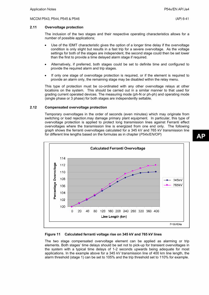
Application Notes P54x/EN AP/Ja4 MiCOM P543, P544, P545 & P546
(AP) 6-41
2.11 Overvoltage protection
The inclusion of the two stages and their respective operating characteristics allows for a number of possible applications;
• Use of the IDMT characteristic gives the option of a longer time delay if the overvoltage condition is only slight but results in a fast trip for a severe overvoltage. As the voltage settings for both of the stages are independent, the second stage could then be set lower than the first to provide a time delayed alarm stage if required.
• Alternatively, if preferred, both stages could be set to definite time and configured to provide the required alarm and trip stages.
• If only one stage of overvoltage protection is required, or if the element is required to provide an alarm only, the remaining stage may be disabled within the relay menu.
This type of protection must be co-ordinated with any other overvoltage relays at other locations on the system. This should be carried out in a similar manner to that used for grading current operated devices. The measuring mode (ph-N or ph-ph) and operating mode (single phase or 3 phase) for both stages are independently settable.
2.12 Compensated overvoltage protection
Temporary overvoltages in the order of seconds (even minutes) which may originate from switching or load rejection.may damage primary plant equipment. In particular, this type of overvoltage protection is applied to protect long transmission lines against Ferranti effect overvoltages where the transmission line is energized from one end only. The following graph shows the ferranti overvoltages calculated for a 345 kV and 765 kV transmission line for different line lengths based on the formulas as in chapter (P54x/EN/OP) AP
Figure 11 Calculated ferranti voltage rise on 345 kV and 765 kV lines
The two stage compensated overvoltage element can be applied as alarming or trip elements. Both stages’ time delays should be set not to pick-up for transient overvoltages in the system with a typical time delays of 1-2 seconds upwards being adequate for most applications. In the example above for a 345 kV transmission line of 400 km line length, the alarm threshold (stage 1) can be set to 105% and the trip threshold set to 110% for example.

P54x/EN AP/Ja4 Application Notes (AP) 6-42
MiCOM P543, P544, P545 & P546
2.13 Residual overvoltage (neutral displacement) protection
On a healthy three phase power system, the addition of each of the three phase to earth voltages is nominally zero, as it is the vector addition of three balanced vectors at 120° to one another. However, when an earth (ground) fault occurs on the primary system this balance is upset and a ‘residual’ voltage is produced.
Note: This condition causes a rise in the neutral voltage with respect to earth which is commonly referred to as neutral voltage displacement or NVD.
Figure 12 and Figure 13 show the residual voltages that are produced during earth fault conditions occurring on a solid and impedance earthed power system respectively.
� ��� �1
�
��2�3
4�
4�4)
4�
4�4) 4) 4�
4�
4)
4���
4���4�
4)
4�
4�
4�
4)
��������5����*�������6��������� �7�������� �� ���� �� +�1 �����8
4������� ��� ��1� � 1�9 9 9
: , ������
3
�
����(�'�
AP
�
Figure 12 Residual voltage, solidly earthed system
As shown in Figure 12 the residual voltage measured by a relay for an earth fault on a solidly earthed system is solely dependent upon the ratio of source impedance behind the relay to line impedance in front of the relay, up to the point of fault. For a remote fault, the Zs/Zl ratio will be small, resulting in a correspondingly small residual voltage. As such, depending upon the relay setting, such a relay would only operate for faults up to a certain distance along the system. The value of residual voltage generated for an earth fault condition is given by the general formula shown.

Application Notes P54x/EN AP/Ja4 MiCOM P543, P544, P545 & P546
(AP) 6-43
AP
��2�3
�
�
3
��
��� �1
� �
4��2�3�
3;�
4)�2�3 4��2�3
4)�2�34��2�3
�4��2�33;� 3;�
4��2�3
4)�2�3
4���
4��2�3
4)�2�3
4��2�3
4���
4��2�3
4)�2�3
4��2�3
4���
4)�2�3
4��2�3
4������� ��� ��1� � 1�9 9 9
: , ������
���9
���9
����%�'�
�
Figure 13 Residual voltage, resistance earthed system
Figure 13 shows that a resistance earthed system will always generate a relatively large degree of residual voltage, as the zero sequence source impedance now includes the earthing impedance. It follows then, that the residual voltage generated by an earth fault on an insulated system will be the highest possible value (3 x phase-neutral voltage), as the zero sequence source impedance is infinite.
The detection of a residual overvoltage condition is an alternative means of earth fault detection, which does not require any measurement of zero sequence current. This may be particularly advantageous at a tee terminal where the infeed is from a delta winding of a transformer (and the delta acts as a zero sequence current trap).
Note: Where residual overvoltage protection is applied, such a voltage will be generated for a fault occurring anywhere on that section of the system and hence the NVD protection must co-ordinate with other earth/ground fault protection.

P54x/EN AP/Ja4 Application Notes (AP) 6-44
MiCOM P543, P544, P545 & P546
AP
2.13.1 Setting guidelines
The voltage setting applied to the elements is dependent upon the magnitude of residual voltage that is expected to occur during the earth fault condition. This in turn is dependent upon the method of system earthing employed and may be calculated by using the formulae previously given in Figure 12 and Figure 13. It must also be ensured that the relay is set above any standing level of residual voltage that is present on the system.
Note: IDMT characteristics are selectable on the first stage of NVD in order that elements located at various points on the system may be time graded with one another.
2.14 Circuit breaker fail protection (CBF)
2.14.1 Breaker fail timer settings
Typical timer settings to use are as follows:
CB fail reset mechanism tBF time delay Typical delay for 2 ½
cycle circuit breaker
Initiating element reset CB interrupting time + element reset time (max.) + error in tBF timer + safety margin
50 + 45 + 10 + 50 = 155 ms
CB open
CB auxiliary contacts opening/closing time (max.) + error in tBF timer + safety margin
50 + 10 + 50 = 110 ms
Undercurrent elements
CB interrupting time + undercurrent element (max.) + safety margin
50 + 25 + 50 = 125 ms
Note: All CB Fail resetting involves the operation of the undercurrent elements. Where element reset or CB open resetting is used the undercurrent time setting should still be used if this proves to be the worst case.
The examples above consider direct tripping of a 2½ cycle circuit breaker.
Note: Where auxiliary tripping relays are used, an additional 10-15 ms must be added to allow for trip relay operation.
2.14.2 Breaker fail undercurrent settings
The phase undercurrent settings (I<) must be set less than load current, to ensure that I< operation indicates that the circuit breaker pole is open. A typical setting for overhead line or cable circuits is 20% In, reduced to 10% or 5% where the infeed has a high SIR ratio (e.g. at a spur terminal with embedded generation infeed).
The sensitive earth fault protection (SEF) undercurrent element must be set less than the respective trip setting, typically as follows:
ΙSEF< = (ΙSEF> trip) / 2

Application Notes P54x/EN AP/Ja4 MiCOM P543, P544, P545 & P546
(AP) 6-45
AP
2.15 Broken conductor detection
The majority of faults on a power system occur between one phase and ground or two phases and ground. These are known as shunt faults and arise from lightning discharges and other overvoltages which initiate flashovers. Alternatively, they may arise from other causes such as birds on overhead lines or mechanical damage to cables etc. Such faults result in an appreciable increase in current and hence in the majority of applications are easily detectable.
Another type of unbalanced fault that can occur on the system is the series or open circuit fault. These can arise from broken conductors, maloperation of single phase switchgear, or single-phasing of fuses. Series faults will not cause an increase in phase current on the system and hence are not readily detectable by standard protection. However, they will produce an unbalance and a resultant level of negative phase sequence current, which can be detected.
It is possible to apply a negative phase sequence overcurrent relay to detect the above condition. However, on a lightly loaded line, the negative sequence current resulting from a series fault condition may be very close to, or less than, the full load steady state unbalance arising from CT errors, load unbalance etc. A negative sequence element therefore would not operate at low load levels.
2.15.1 Setting guidelines
For a broken conductor affecting a single point earthed power system, there will be little zero sequence current flow and the ratio of Ι2/Ι1 that flows in the protected circuit will approach 100%. In the case of a multiple earthed power system (assuming equal impedance’s in each sequence network), the ratio Ι2/Ι1 will be 50%.
In practice, the levels of standing negative phase sequence current present on the system govern this minimum setting. This can be determined from a system study, or by making use of the relay measurement facilities at the commissioning stage. If the latter method is adopted, it is important to take the measurements during maximum system load conditions, to ensure that all single-phase loads are accounted for.
Note: A minimum value of 8% negative phase sequence current is required for successful relay operation.
Since sensitive settings have been employed, it can be expected that the element will operate for any unbalance condition occurring on the system (for example, during a single pole auto-reclose cycle). Hence, a long time delay is necessary to ensure co-ordination with other protective devices. A 60 second time delay setting may be typical.
The example following information was recorded by the relay during commissioning;
Ιfull load = 500 A
Ι2 = 50 A
therefore the quiescent Ι2/Ι1 ratio is given by;
Ι2/Ι1 = 50/500 = 0.1
To allow for tolerances and load variations a setting of 20% of this value may be typical: Therefore set Ι2/Ι1 = 0.2
In a double circuit (parallel line) application, using a 40% setting will ensure that the broken conductor protection will operate only for the circuit that is affected. Setting 0.4 results in no pick-up for the parallel healthy circuit.
Set Ι2/Ι1 Time Delay = 60 s to allow adequate time for short circuit fault clearance by time delayed protections.

P54x/EN AP/Ja4 Application Notes (AP) 6-46
MiCOM P543, P544, P545 & P546
AP
2.16 Communication between relays
2.16.1 Optical budgets
When applying any of the P54x range of current differential relays it is important to select the appropriate protection communications interface. This will depend on the fiber used and distance between devices. The following table shows the optical budgets of the available communications interfaces.
From April 2008 850 nm Multi mode
1300 nm Multi mode
1300 nm Single mode
1550 nm Single mode
Min. transmit output level (average power) -19.8 dBm -6 dBm -6 dBm -6 dBm
Receiver sensitivity (average power) -25.4 dBm -49 dBm -49 dBm -49 dBm
Optical budget 5.6 dB 43.0 dB 43.0 dB 43.0 dB
Less safety margin (3 dB) 2.6 dB 40.0 dB 40.0 dB 40.0 dB
Typical cable loss 2.6 dB/km 0.8 dB/km 0.4 dB/km 0.3 dB/km
Max. transmission distance 1 km 50.0 km 100.0 km 130 km
Note: From April 2008, the optical budgets and hence also the maximum transmission distances of the 1300 nm multi-mode, 1300 nm single-mode and 1550 nm single-mode fiber interfaces have been increased, to the values shown in the table above.
The new interface cards are identified by “43dB” marked in the centre of the backplate, visible from the rear of the relay. These new fiber interfaces are fully backward-compatible with the original equivalent interface. However, in order to achieve the increased distance, both/all ends of the P54x scheme would need to use the new interface.
Pre-April 2008 relays will have the original optical budgets and maximum transmission distances, as shown below.
Pre-April 2008 850 nm Multi mode
1300 nm Multi mode
1300 nm Single mode
1550 nm Single mode
Min. transmit output level (average power) -19.8 dBm -10 dBm -10 dBm -10 dBm
Receiver sensitivity (average power) -25.4 dBm -37 dBm -37 dBm -37 dBm
Optical budget 5.6 dB 27.0 dB 27.0 dB 27.0 dB
Less safety margin (3dB) 2.6 dB 24.0 dB 24.0 dB 24.0 dB
Typical cable loss 2.6 dB/km 0.8 dB/km 0.4 dB/km 0.3 dB/km
Max. transmission distance 1 km 30.0 km 60.0 km 80 km
The total optical budget is given by transmitter output level minus the receiver sensitivity and will indicate the total allowable losses that can be tolerated between devices. A safety margin of 3 dB is also included in the above table. This allows for degradation of the fiber as a result of ageing and any losses in cable joints. The remainder of the losses will come from the fiber itself. The figures given are typical only and should only be used as a guide.
In general, the 1300 nm and 1550 nm interfaces will be used for direct connections between relays. The 850 nm would be used where multiplexing equipment is employed.

Application Notes P54x/EN AP/Ja4 MiCOM P543, P544, P545 & P546
(AP) 6-47
AP
2.16.2 Clock source setting
The Clock Source should be set to “Internal” at all system ends, where they are connected by direct optical fiber, as the P54x at each end has to supply the clock.
The Clock Source should be set to External at all system ends, where the ends are connected by multiplexer equipment which is receiving a master clock signal from the multiplexer network. It is important that there is a single master clock source on the multiplexer network and that the multiplexer equipment at each end is synchronized to this clock.
Note: This setting is not applicable if IEEE C37.94 mode selected.
2.16.3 Data rate
The data rate for signaling between the two or three ends may be set to either 64 kbit/sec or 56 kbit/sec as appropriate.
If there is a direct fiber connection between the ends, the data rate would usually be set to 64 kbit/sec, as this gives a slightly faster trip time.
If there is a multiplexer network between the ends, then this will determine the data rate to be used by the P54x system. The electrical interface to the multiplexer (G.703 co-directional, V.35, or X.21) will be provided on either a 64 kbit/sec or 56 kbit/sec channel, and the P54x at each end must be set to match this data rate.
Generally, North American multiplexer networks are based on 56 kbit/sec (and multiples thereof) channels, whereas multiplexer networks in the rest of the world are based on 64 kbit/sec (and multiples thereof) channels.
This setting is not applicable if IEEE C37.94 mode selected.
2.17 InterMiCOM64 (“Fiber InterMiCOM”) The protection signaling channels of the P54x primarily intended to provide the capability for implementing current differential protection are also capable of supporting InterMiCOM64 teleprotection. If the P54x is configured to provide differential protection, then the InterMiCOM64 commands (IMx command) are transmitted together with the current differential signals. If the differential protection of the P54x is not being employed, then the communications messages are restructured to provide InterMiCOM64 signaling of the type supported by the MiCOMho P446, P443 and P445 relays. In either case, the fundamental operation of the InterMiCOM64 commands is the same.
2.17.1 IMx command type Due to the fast data rate, there is not so much difference in real performance between the three generic modes of teleprotection (Direct Intertrip, Permissive and Blocking), so only two are implemented for InterMiCOM64. Direct Intertripping is available, with the second mode a combined mode for Permissive/Blocking (the latter is named as ‘Permissive’ in the menu). To increase the security for Intertripping (Direct transfer tripping), the InterMiCOM64 Direct command is issued only when 2 valid consecutive messages are received. The recommended setting is:
• For Blocking schemes set ‘Permissive’
• For Permissive scheme set ‘Permissive’
• For Transfer (inter)tripping set ‘Direct’ The setting files provide independent setting for each of the first 8 commands. Due to the fast data rate, there will be minimal speed difference between the two mode options. Both will give a typical operating time (PSL trigger at the send relay, to PSL state change at the receive relay) as shown below:

P54x/EN AP/Ja4 Application Notes (AP) 6-48
MiCOM P543, P544, P545 & P546
AP
Channel mode
setting Application Typical delay
(ms) Maximum
(ms) Comments
Direct Fiber 3 to 7 9 Assuming no repeaters (no source of digital “noise”) Permissive
Multiplexed Link 5 to 8 + MUX 12 + MUX For channel bit error rate up to 1 x 10⁻³
Direct Fiber 4 to 8 10 Assuming no repeaters (no source of digital “noise”) Direct
Intertrip Multiplexed link 6 to 8 + MUX 13 + MUX For channel bit error
rate up to 1 x 10⁻³
These figures are for InterMiCOM64 used as a standalone feature. For use with differential message, add 2 ms for permissive mode and 4 ms for direct intertrip at 64 Kb/sec. When using InterMiCOM64 to implement Aided Scheme 1 or Aided Scheme 2, it is suggested to assume a conservative worst-case channel delay of 15 ms (pickup and reset delay), for the purposes of blocking and reversal guard calculations. The delay of the multiplexer should be added if applicable, taking into account longer standby path re-routings which might be experienced in the event of self-healing in a SONET/SDH telecomms network. When using InterMiCOM64 as a standalone feature in 3-terminal applications, where fallback to “chain” topology is possible in the event of failure of one communications leg in the triangle, longer times may be experienced. In fallback mode, retransmission of the messages occurs so the path length is doubled. Overall command times to the final end can be doubled.
2.17.2 IMx fallback mode
When the ‘Default’ setting is selected, the following ‘IMx Default Value’ settings are recommended: For Intertripping schemes set 0, for Blocking schemes set 1. In Permissive applications, the user may prefer to latch the last healthy received state for a period of time.

Application Notes P54x/EN AP/Ja4 MiCOM P543, P544, P545 & P546
(AP) 6-49
3. WORKED PROTECTION EXAMPLE AND OTHER PROTECTION TIPS
3.1 Differential protection setting examples
3.1.1 Differential element
All four settings are user adjustable. This flexibility in settings allows the relay characteristic to be tailored to suit particular sensitivity and CT requirements. To simplify the protection engineer’s task, we strongly recommend three of the settings be fixed to:
Ιs2 = 2.0 pu
k1 = 30%
k2 = 150% (2 terminal applications) or 100% (3 terminal applications)
These settings will give a relay characteristic suitable for most applications. It leaves only the Is1 setting to be decided by the user. The value of this setting should be in excess of any mismatch between line ends, if any, and should also account for line charging current, where necessary.
By considering the circuit shown in Figure 14, the settings for the phase current differential element can be established.
��<4 ��<����+� ���+�
��<4
=�*��������� ������ ���� <
�����������������*� *����� � :��8���+<��2�����:��8���+<��2��5��������� � ����������������
AP
Figure 14 Typical plain feeder circuit
The following settings should be set as follows:
Ιs2 = 2.0 pu
k1 = 30%
k2 = 150% (for a two terminal application)
This leaves the setting of Ιs1 to be established.
In the case that voltage inputs are not in place, no facility to account for line charging current is available. The setting of Ιs1 must therefore be set above 2.5 times the steady state charging current value. In this example, assume a cable is used and there are not VT inputs connected to the relay:
Ιs1 > 2.5 x Ιch
Ιs1 > 2.5 x (25km x 2.5 A/km)
Ιs1 > 156.25 A
The line CTs are rated at 400 amps primary. The setting of Ιs1 must therefore exceed 156.25/400 = 0.391 pu.
Therefore select:
Ιs1 = 0.4 pu
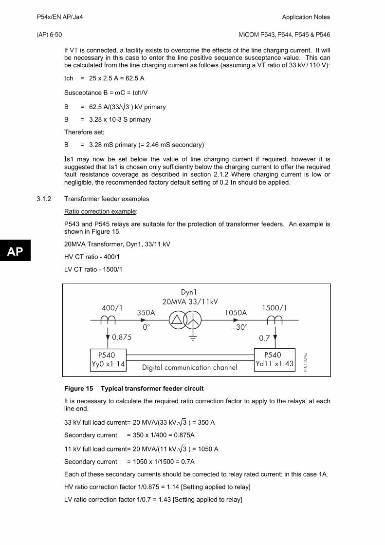
P54x/EN AP/Ja4 Application Notes (AP) 6-50
MiCOM P543, P544, P545 & P546
If VT is connected, a facility exists to overcome the effects of the line charging current. It will be necessary in this case to enter the line positive sequence susceptance value. This can be calculated from the line charging current as follows (assuming a VT ratio of 33 kV / 110 V):
Ιch = 25 x 2.5 A = 62.5 A
Susceptance B = ωC = Ιch/V
B = 62.5 A/(33/ 3 ) kV primary
B = 3.28 x 10⁻³ S primary
Therefore set:
B = 3.28 mS primary (= 2.46 mS secondary)
Ιs1 may now be set below the value of line charging current if required, however it is suggested that Is1 is chosen only sufficiently below the charging current to offer the required fault resistance coverage as described in section 2.1.2 Where charging current is low or negligible, the recommended factory default setting of 0.2 Ιn should be applied.
3.1.2 Transformer feeder examples
Ratio correction example:
P543 and P545 relays are suitable for the protection of transformer feeders. An example is shown in Figure 15.
20MVA Transformer, Dyn1, 33/11 kV AP HV CT ratio - 400/1
LV CT ratio - 1500/1
=�*��������� ������ ���� ��
���+����� �����
�8��� �8�
����+�
�> ?��>
=� ���@4����+��<4
�������
�
A���,�8�� A����,�8��
Figure 15 Typical transformer feeder circuit
It is necessary to calculate the required ratio correction factor to apply to the relays’ at each line end.
33 kV full load current = 20 MVA/(33 kV. 3 ) = 350 A
Secondary current = 350 x 1/400 = 0.875A
11 kV full load current = 20 MVA/(11 kV. 3 ) = 1050 A
Secondary current = 1050 x 1/1500 = 0.7A
Each of these secondary currents should be corrected to relay rated current; in this case 1A.
HV ratio correction factor 1/0.875 = 1.14 [Setting applied to relay]
LV ratio correction factor 1/0.7 = 1.43 [Setting applied to relay]

Application Notes P54x/EN AP/Ja4 MiCOM P543, P544, P545 & P546
(AP) 6-51
When a Star/Delta software interposing CT is chosen, no additional account has to be taken for the 3 factor which would be introduced by the delta winding. This is accounted for by the relay.
Phase Correction Example:
Using the same transformer as shown in Figure 15 it is now necessary to correct for the phase shift between the HV and LV windings.
The transformer connection shows that the delta connected high voltage line current leads the low voltage line current by 30°. To ensure that this phase shift does not create a differential current, the phase shift must be corrected in the LV secondary circuit. The LV relay software interposing CT is effectively a winding replica of the main power transformer. It not only provides a +30° phase shift, but also performs the necessary function of filtering out any LV zero sequence current component.
Hence, the HV relay setting requires no phase shift or zero sequence current filtering (as HV winding is delta connected). The LV relay setting requires phase shifting by +30° and also requires zero sequence current filtering (as LV winding is star connected).
Set: HV = Yy0
LV = Yd11 (+30°)
It is important when considering the software ICT connection, to account for both the phase shift and zero sequence current filtering. For example, with the transformer in Figure 15, it would have been possible to provide phase compensation by applying Yd1 and Yy0 settings to the HV and LV relays respectively. Although this provides correct phase shift compensation, no zero sequence current filtering exists on the LV side and hence relay maloperation could occur for an external earth fault. AP
3.1.3 Teed feeder example
������� ��
��
��� ���!
���
���!
���!
���
������
����������
���� ����
����������
����������
�����
�� ���������"���������#
�� ���������"���������#�� ���������"���������#
$�����$�������� � ��"����%�&'()��*+��,��������
�����
- (&!./�
Figure 16 Typical teed feeder application
If there are not VT inputs connected, P54x relays have not facilities to account for charging line current, therefore the setting Is1 must be 2.5 times the steady state charging current.
If VT inputs are connected, there is a facility to overcome the effect of charging current. As mentioned before, it is necessary to enter the positive sequence susceptance value.
P54x/EN AP/Ja4 Application Notes (AP) 6-52
MiCOM P543, P544, P545 & P546
AP
Considering the charging current on the circuit shown in Figure 16, the following calculation is done:
• Ich = 0.58 A ( 45 + 30 + 10 ) = 49.3 A
• Susceptance = ω C = Ich/V
• B = 49.3 A/( 275/ √3) kV primary
• B = 0.31 x 10⁻³ S primary.
As the CT ratio on the three ends are different, it is necessary to apply a correction factor in order to ensure secondary currents balance for all conditions:
To calculate the correction factor (CF), the same primary current must be used even this current is not the expected load transfer for every branch. This will ensure secondary current balance for all conditions.
A good approximation to calculate the correction factor, would be to use the primary rated current of the smallest CT ratio as a base current. In this case we will use the primary rated CT current at End C, in order to correct the secondary currents to the relay rated current:
For End A 1200 A
Secondary current =1200x 5/4000 = 1.5 A
CF = 5/1.5 = 3.33
For End B 1200 A
Secondary current =1200x 5/4000 = 1.5 A
CF = 5/1.5 = 3.33
For End C 1200 A prim = 5 A sec
Secondary current =1200x 5/1200 = 5 A
CF = 5/5 = 1
As mentioned on example 3.1.1, the following settings are recommended:
Is1 = 0.2 In
Is2 = 2 In
K1 = 30%
K2 = 100%
Therefore, settings in secondary values for each end are:
Is1 = 0.2In =1 A
Is2 = 2In =10 A
Note: Settings shown in primary values at ends A and B appear different compared with end C. This is not a problem as the currents at ends A and B will be multiplied by the Correction Factor, when the differential calculation is done. There would not be a requirement to alter settings by CF as the relay works in secondary values.

Application Notes P54x/EN AP/Ja4 MiCOM P543, P544, P545 & P546
(AP) 6-53
Susceptance settings:
For Ends A and B
With a VT ratio 275 kV/110 V and CT ratio 4000/5
RCT = 800
RVT = 2500
B = 310 μS
Secondary susceptance = 310 μS x RVT/ RCT = 968 μS
For End C
With a VT ratio 275 kV/110 V and CT ratio 1200/5
B = 310 μS
Secondary susceptance = 310 μS x RVT/ RCT = 3.22 mS sec.
3.1.4 Three winding transformer in zone with different rated CTs example
P543 and P545 relays are suitable for the protection of three winding transformers in zone. An example is shown in Figure 17.
100 MVA/100MVA/30MVA Transformer, Ynyn0d1, 400 kV/110 kV/30 kV
HV, 400 kV CT ratio - 600/1
AP MV, 110 kV CT ratio - 1200/1
LV, 30 kV CT ratio - 2000/5
�������������
�����������
��� ���!
���
���!���
���!
����������
����������������
�� ���������"���������#
�� ���������"���������#�� ���������"���������#
������
- (&0./�
�������������
�������������������������
Figure 17 Three winding transformer in zone application
These three relays must be rated differently, i.e. 1A for HV and MV side and 5 A for 30 kV side. This does not present a problem for P54x relays as the digital signals representing the currents are in pu.
P54x/EN AP/Ja4 Application Notes (AP) 6-54
MiCOM P543, P544, P545 & P546
AP
It is necessary to calculate the required ratio correction factor (CF) as well as the phase correction factor for each end. To choose the appropriate vector compensation, it is necessary to account for phase current and zero sequence current filtering as explained in example 3.1.2.
To calculate the correction factor range, it is necessary to use the same MVA base for the three sides of the transformer although the third winding actually has a lower rated MVA. This is to ensure secondary current balance for all conditions.
For HV side: 100 MVA/ (400 kV.√3) = 144.34 A.
Secondary current = 144.34 x 1/600 = 0.24 A
For MV side: 100 MVA/ (110 kV.√3) = 524.86 A.
Secondary current = 524.86 x 1/1200 = 0.44 A
For LV side: 100 MVA/ (30 kV.√3) = 1924.5 A.
Secondary current = 1924.5x 5/2000 = 4.81 A
Each secondary current should be corrected to relay rated current, in this case 1A for HV and MV side and 5 A for 30 kV side
HV ratio correction factor = 1/0.24 = 4.16
MV ratio correction factor = 1/0.44 = 2.29
LV ratio correction factor = 5/4.81 = 1.04
To choose the vector compensation connection, it should be noted that the Wye connected HV line is in phase with the MV line current and leads the LV line current by 30o. Therefore for LV side, the phase shift must be compensated.
To account for the zero sequence current filtering in the case of an external earth fault, it is necessary to connect the Wye connected power transformer windings to an interposing current transformer (internal relay ICT) to trap the zero sequence current (the secondary side being connected delta).
To account for both vector compensation and zero sequence current filtering, the following vectorial compensation setting is recommended:
• For HV side = Yd1 (-30 deg)
• For MV side = Yd1 (-30 deg)
• For LV side = Yy0 (0 deg)
Note: It is not necessary to include the √3 factor in the calculation as this is incorporated in the relay algorithm.
P543 and P545 relays are suitable for transformer applications, as such an inrush restrain is provided on these relay models. By enabling inrush restrain, an additional current differential high setting (Id High set) becomes enable.
When the inrush restrain feature is enabled, it is necessary that this function is enabled in the relay at each line end (3 ends).
For the differential calculation the same recommended settings for the previous examples are recommended:
• Is1 = 0.2 In
• Is2 = 2 In
• K1 = 30%
• K2 = 100%

Application Notes P54x/EN AP/Ja4 MiCOM P543, P544, P545 & P546
(AP) 6-55
Therefore, settings in secondary values are:
For relays rated to 1 A (HV and MV sides) Is1 = 200 mA and Is2 = 2 A
For relay rated to 5 A (LV side) Is1 = 1 A and Is2 = 10 A
For the current differential high setting (Id High set) the setting must be in excess of the anticipated inrush current after ratio correction. Assuming that maximum inrush is 12 times the nominal transformer current, it would be safe to set the relays at 15 times the nominal current, therefore the setting would be:
• Id high set : for HV side = 15 In = 15 A
for MV side = 15 In = 15 A
for LV side = 15 In = 75 A
3.2 Distance protection setting example
3.2.1 Objective
To protect the 100 km double circuit line between Green Valley and Blue River substations using a MiCOM P54x in distance POR Permissive Overreach mode and to set the relay at Green Valley substation, shown in Figure 18. It is assumed that mho characteristics will be used.
AP ��<� �<�
���<�
�� ��
!�*������ 3��� �4����� ������5�� ���<�����
�����������3��� �4������2�������5������ ������� ��� ��������5����*�����<5�������*�� �� *������)!�����������+�4!�������������+���1� ���� *������<�1� �������� �����:��8����9�B�8�� �-C@+<����:��8�� �9�B�8�� �-C@+<��������5����3��� �4������������� ��������,��������@4�;��� ��������@4�������5���������� ��������,��������@4�;��� ��������@4�)�������� �� ������� *� ����:����@4�D����2�������E���F�������F������:��8�� �������
��������
Figure 18 System assumed for worked example

P54x/EN AP/Ja4 Application Notes (AP) 6-56
MiCOM P543, P544, P545 & P546
3.2.2 System data
Line length: 100 km
= 0.089 + j0.476 = 0.484 ∠79.4° Ω/km Line impedances: Z1
Z = 0.426 + j1.576 = 1.632 ∠74.8° Ω/km 0
Z
AP
0/Z = 3.372 ∠-4.6° 1
CT ratio: 1 200/5
VT ratio: 230 000/115
3.2.3 Relay settings
It is assumed that Zone 1 Extension is not used and that only three forward zones are required. Settings on the relay can be performed in primary or secondary quantities and impedances can be expressed as either polar or rectangular quantities (menu selectable). For the purposes of this example, secondary quantities are used.
3.2.4 Line impedance
Ratio of secondary to primary impedance = 1200 / 5
230000 / 115 = 0.12
Line impedance secondary = ratio CT/VT x line impedance primary.
Line Impedance = 100 x 0.484 ∠79.4° (primary) x 0.124
= 5.81 ∠79.4° Ω secondary.
Select Line Angle = 80° for convenience.
Therefore set Line Impedance and Line Angle: = 5.81 ∠80° Ω secondary.
3.2.5 Residual compensation for ground fault elements
The residual compensation factor can be applied independently to certain zones if required. This feature is useful where line impedance characteristics change between sections or where hybrid circuits are used. In this example, the line impedance characteristics do not change and as such a common KZN factor can be applied to each zone. This is set as a ratio “kZN Res. Comp”, and an angle “kZN Angle”:
kZN Res. Comp, ⏐kZN⏐ = (Z0 - Z1) / 3Z1 i.e.: As a ratio
kZN Angle, ∠kZN = ∠ (Z0 - Z1) / 3Z1 Set in degrees
ZL0 - ZL1 = (0.426 + j1.576) - (0.089 + j0.476)
= 0.337 + j1.1
= 1.15 ∠72.9°
°∠×°∠4.79484.03
9.7215.1 = 0.79 ∠–6.5° kZN =
Therefore, select:
kZN Res. Comp = 0.7
kZN Angle = - 6.5°

Application Notes P54x/EN AP/Ja4 MiCOM P543, P544, P545 & P546
(AP) 6-57
AP
3.2.6 Zone 1 phase and ground reach settings
Required Zone 1 reach is to be 80% of the line impedance between Green Valley and Blue River substations.
Setting the Relay in the SIMPLE setting mode (recommended):
• Set Zone 1 Ph and Zone 1 Gnd reach = 80%
From this the relay will automatically calculate the required ohmic reaches, or they can be entered manually in the ADVANCED mode, as follows:
Required Zone 1 reach = 0.8 x 100 x 0.484 ∠79.4° x 0.12
Z1 = 4.64 ∠79.4° Ω secondary
The Line Angle = 80°
Therefore actual Zone 1 reach, Z1 = 4.64 ∠80° Ω secondary.
3.2.7 Zone 2 phase and ground reach settings
Required Zone 2 impedance = (Green Valley-Blue River) line impedance + 50% (Blue River-Rocky Bay) line impedance
Z2 = (100+30) x 0.484 ∠79.4° x 0.12 = 7.56 ∠79.4° Ω secondary.
The Line Angle = 80°
Actual Zone 2 reach setting = 7.56 ∠80° Ω secondary
Alternatively, in SIMPLE setting mode, this reach can be set as a percentage of the protected line. Typically a figure of at least 120% is used.
3.2.8 Zone 3 phase and ground reach settings
Required Zone 3 forward reach = (Green Valley-Blue River + Blue River-Rocky Bay) x 1.2
= (100+60) x 1.2 x 0.484 ∠79.4° x 0.12
Z3 = 11.15 ∠79.4° ohms secondary
Actual Zone 3 forward reach setting = 11.16 ∠80° ohms secondary
Alternatively, in SIMPLE setting mode, this reach can be set as a percentage of the protected line.
3.2.9 Zone 3 reverse reach
In the absence of other special requirements, Zone 3 can be given a small reverse reach setting, of Z3’ = 10%. This is acceptable because the protected line length is > 30km.
Zone 4 Reverse Settings with POR and BLOCKING schemes
Where zone 4 is used to provide reverse directional decisions for Blocking or Permissive Overreach schemes, zone 4 must reach further behind the relay than zone 2 for the remote relay. This can be achieved by setting: Z4 ≥ ((Remote zone 2 reach) x 120%), where mho characteristics are used.

P54x/EN AP/Ja4 Application Notes (AP) 6-58
MiCOM P543, P544, P545 & P546
AP
Remote Zone 2 reach = (Blue River-Green Valley) line impedance + 50%n (Green Valley-Tiger Bay) line impedance
= (100+40) x 0.484 ∠79.4° x 0.12
= 8.13 ∠79.4° Ω secondary
Z4 ≥ ((8.13 ∠79.4°) x 120%) - (5.81 ∠79.4°)
= 3.95 ∠79.4°
Minimum zone 4 reverse reach setting = 3.96 ∠80° ohms secondary
3.2.10 Load avoidance
The maximum full load current of the line can be determined from the calculation:
IFLC = [(Rated MVAFLC) / (√3 x Line kV)]
In practice, relay settings must allow for a level of overloading, typically a maximum current of 120% IFLC prevailing on the system transmission lines. Also, for a double circuit line, during the auto-reclose dead time of fault clearance on the adjacent circuit, twice this level of current may flow on the healthy line for a short period of time. Therefore the circuit current loading could be 2.4 x IFLC.
With such a heavy load flow, the system voltage may be depressed, typically with phase voltages down to 90% of Vn nominal.
Allowing for a tolerance in the measuring circuit inputs (line CT error, VT error, relay tolerance, and safety margin), this results in a load impedance which might be 3 times the expected “rating”.
To avoid the load, the blinder impedance needs to be set:
Z ≤ (Rated phase-ground voltage Vn) / (IFLC x 3)
= (115/√3) / (IFLC x 3)
Set the V< Blinder voltage threshold at the recommended 70% of Vn = 66.4 x 0.7 = 45 V.
3.2.11 Additional settings for quadrilateral applications
3.2.11.1 Phase fault resistive reaches (Rph)
In primary impedance terms, RPh reaches must be set to cover the maximum expected phase-to-phase fault resistance. Ideally, RPh must be set greater than the maximum fault arc resistance for a phase-phase fault, calculated as follows:
Ra = (28710 x L)/If 1.4
Where:
If = Minimum expected phase-phase fault current (A);
L = Maximum phase conductor separation (m);
Ra = Arc resistance, calculated from the van Warrington formula (Ω).
Typical figures for Ra (primary Ω) are given in the table below, for different values of minimum expected phase fault current.
Conductor spacing (m)
Typical system voltage (kV) If = 1 kA If = 2 kA If = 3 kA
4 110 - 132 7.2 Ω 2.8 Ω 1.6 Ω
8 220 - 275 14.5 Ω 5.5 Ω 3.1 Ω
11 380 - 400 19.9 Ω 7.6 Ω 4.3 Ω
Application Notes P54x/EN AP/Ja4 MiCOM P543, P544, P545 & P546
(AP) 6-59
AP
Note: Dual-end infeed effects will make a fault resistance appear higher, because each relay cannot measure the current contribution from the remote line end. The apparent fault resistance increase factor could be 2 to 8 times the calculated resistance. Therefore it is recommended that the Zone resistive reaches are set to say, 4 times the primary arc resistance calculation.
In the example, the minimum phase fault level is 1000 MVA. This is equivalent to an effective short-circuit fault feeding impedance of:
Z = kV 2/MVA = 2302/1000 = 53 Ω (primary)
The lowest phase fault current level is equivalent to:
Ifault = (MVA x 1000)/(√3 x kV)
= (1000 x 1000)/(√3 x 230)
= 2.5 kA
And this fault current in the van Warrington formula would give an arc resistance of:
Ra = 4 Ω
As this impedance is relatively small compared to the value “Z” calculated above, there is no need to perform an iterative equation to work out the actual expected Ifault (which would in reality be lower due to the added Ra arc resistance in the fault loop). It will suffice to increase the calculated Ra by the recommended factor of four, and a little extra to account for the fault current being lower than that calculated. So, in this case use a minimum setting of 5 x Ra, which is 20 Ω primary.
It is obvious that the setting could easily be set above 20 Ω on the primary system (perhaps following the rule of thumb formula in section 2.3.7). Typically, all zone resistive reaches would be set greater than this 20 Ω primary figure, and ideally less than the load impedance (see “load avoidance” section).
3.2.11.2 Ground fault resistive reaches (RGnd)
Fault resistance would comprise arc-resistance and tower footing resistance. A typical resistive reach coverage setting would be 40 Ω on the primary system.
For high resistance earth faults, the situation may arise where no distance elements could operate. In this case it will be necessary to provide supplementary earth fault protection, for example using the relay Channel Aided DEF protection. In such cases it is not essential to set large resistive reaches for ground distance, and then RGnd can be set according to the rule of thumb formula in section 2.3.8.
3.3 Teed feeder protection
The application of distance relays to three terminal lines is fairly common. However, several problems arise when applying distance protection to three terminal lines.
3.3.1 The apparent impedance seen by the distance elements
Figure 19 shows a typical three terminal line arrangement. For a fault at the busbars of terminal B the impedance seen by a relay at terminal A will be equal to:
Za = Zat + Zbt + [Zbt.(Ic/Ia)]
Relay A will underreach for faults beyond the tee-point with infeed from terminal C. When terminal C is a relatively strong source, the underreaching effect can be substantial. For a zone 2 element set to 120% of the protected line, this effect may result in non-operation of the element for internal faults. This not only effects time delayed zone 2 tripping but also channel-aided schemes. Where infeed is present, it will be necessary for Zone 2 elements at all line terminals to overreach both remote terminals with allowance for the effect of tee-point infeed. Zone 1 elements must be set to underreach the true impedance to the nearest terminal without infeed. Both these requirements can be met through use of the alternative setting groups.

P54x/EN AP/Ja4 Application Notes (AP) 6-60
MiCOM P543, P544, P545 & P546
�� �
��
� �
)
��� ��
���
4� : ����� 9� ��
� : ��9 ��
4���
�������
/����� ������ �����������:
��������
Figure 19 Teed feeder application - apparent impedances seen by RELAY
3.3.2 Permissive overreach schemes
To ensure operation for internal faults in a POR scheme, the relays at the three terminals should be able to see a fault at any point within the protected feeder. This may demand very large zone 2 reach settings to deal with the apparent impedances seen by the relays. AP A POR scheme requires the use of two signaling channels. A permissive trip can only be issued upon operation of zone 2 and receipt of a signal from both remote line ends. The requirement for an 'AND' function of received signals must be realized through use of contact logic external to the relay, or the internal Programmable Scheme Logic. Although a POR scheme can be applied to a three terminal line, the signaling requirements make its use unattractive.
3.3.3 Permissive underreach schemes
For a PUR scheme, the signaling channel is only keyed for internal faults. Permissive tripping is allowed for operation of zone 2 plus receipt of a signal from either remote line end. This makes the signaling channel requirements for a PUR scheme less demanding than for a POR scheme. A common power line carrier (PLC) signaling channel or a triangulated signaling arrangement can be used. This makes the use of a PUR scheme for a teed feeder a more attractive alternative than use of a POR scheme.
The channel is keyed from operation of zone 1 tripping elements. Provided at least one zone 1 element can see an internal fault then aided tripping will occur at the other terminals if the overreaching zone 2 setting requirement has been met. There are however two cases where this is not possible:
• Figure 20 (i) shows the case where a short tee is connected close to another terminal. In this case, zone 1 elements set to 80% of the shortest relative feeder length do not overlap. This leaves a section not covered by any zone 1 element. Any fault in this section would result in zone 2 time delayed tripping.
• Figure 20 (ii) shows an example where terminal 'C' has no infeed. Faults close to this terminal will not operate the relay at 'C' and hence the fault will be cleared by the zone 2 time-delayed elements of the relays at 'A' and 'B'.

Application Notes P54x/EN AP/Ja4 MiCOM P543, P544, P545 & P546
(AP) 6-61
�
���
�
)
��):������E����� ��G� �����5�������,����
����
�
���
�
)
���
���� F���
�������� �����H���� �G� ���
� �
)
���������)��������5�����F���� ��������� �
6�7
6��7
6���7
��� ���
��������
AP
Figure 20 Teed feeder applications
Figure 20 (iii) illustrates a further difficulty for a PUR scheme. In this example current is outfed from terminal 'C' for an internal fault. The relay at 'C' will therefore see the fault as reverse and not operate until the breaker at 'B' has opened; i.e. sequential tripping will occur.
3.3.4 Blocking schemes
Blocking schemes are particularly suited to the protection of teed feeders, since high speed operation can be achieved where there is no current infeed from one or more terminals. The scheme also has the advantage that only a common simplex channel or a triangulated simplex channel is required.
The major disadvantage of blocking schemes is highlighted in Figure 20 (iii) where fault current is outfed from a terminal for an internal fault condition. Relay 'C' sees a reverse fault condition. This results in a blocking signal being sent to the two remote line ends, preventing tripping until the normal zone 2 time delay has expired.
P54x/EN AP/Ja4 Application Notes (AP) 6-62
MiCOM P543, P544, P545 & P546
AP
3.4 VT connections
3.4.1 Open delta (vee connected) VT's
The MiCOM P54x relay can be used with vee connected VTs by connecting the VT secondary’s to:
C19, C20 and C21 input terminals, with the C22 input left unconnected for P543 and P544
D19, D20 and D21 input terminals, with the D22 input left unconnected for P545 and P546
This type of VT arrangement cannot pass zero-sequence (residual) voltage to the relay, or provide any phase to neutral voltage quantities. Therefore any protection that is dependent upon phase to neutral voltage measurements should be disabled.
The ground directional comparison elements, ground distance elements, neutral voltage displacement (residual overvoltage) and CT supervision all use phase-to-neutral voltage signals for their operation and should be disabled. The DEF elements should be selected for negative sequence polarization to avoid the use of phase-to-neutral voltages. Under and over voltage protection can be set as phase-to-phase measuring elements, whereas all other protection elements should remain operational.
The accuracy of the single phase voltage measurements can be impaired when using vee connected VT’s. The relay attempts to derive the phase to neutral voltages from the phase to phase voltage vectors. If the impedance of the voltage inputs were perfectly matched the phase to neutral voltage measurements would be correct, provided the phase to phase voltage vectors were balanced. However, in practice there are small differences in the impedance of the voltage inputs, which can cause small errors in the phase to neutral voltage measurements. This may give rise to an apparent residual voltage. This problem also extends to single phase power measurements that are also dependent upon their respective single phase voltages.
The phase to neutral voltage measurement accuracy can be improved by connecting 3, well matched, load resistors between the phase voltage inputs (C19, C20, C21 for P543 and P544 or D19, D20, D21 for P545 and P546) and neutral C22 for P543 and P544 or D22 for P545 and P546 thus creating a ‘virtual’ neutral point. The load resistor values must be chosen so that their power consumption is within the limits of the VT. It is recommended that 10 kΩ ±1% (6 W) resistors are used for the 110 V (Vn) rated relay, assuming the VT can supply this burden.
3.4.2 VT single point earthing
The MiCOM P54x will function correctly with conventional 3 phase VT’s earthed at any one point on the VT secondary circuit. Typical earthing examples being neutral earthing, or B-phase (UK: “yellow phase” earthing).
3.5 Trip circuit supervision (TCS)
The trip circuit, in most protective schemes, extends beyond the relay enclosure and passes through components such as fuses, links, relay contacts, auxiliary switches and other terminal boards. This complex arrangement, coupled with the importance of the trip circuit, has led to dedicated schemes for its supervision.
Several trip circuit supervision scheme variants are offered. Although there are no dedicated settings for TCS, in the MiCOM P54x the following schemes can be produced using the programmable scheme logic (PSL). A user alarm is used in the PSL to issue an alarm message on the relay front display. If necessary, the user alarm can be re-named using the menu text editor to indicate that there is a fault with the trip circuit.

Application Notes P54x/EN AP/Ja4 MiCOM P543, P544, P545 & P546
(AP) 6-63
3.5.1 TCS scheme 1
3.5.1.1 Scheme description
Figure 21 TCS scheme 1
This scheme provides supervision of the trip coil with the breaker open or closed, however, pre-closing supervision is not provided. This scheme is also incompatible with latched trip contacts, as a latched contact will short out the opto for greater than the recommended DDO timer setting of 400 ms. If breaker status monitoring is required a further 1 or 2 opto inputs must be used.
Note: A 52a CB auxiliary contact follows the CB position and a 52b contact is in the opposite state.
AP When the breaker is closed, supervision current passes through the opto input, blocking diode and trip coil. When the breaker is open current still flows through the opto input and into the trip coil via the 52b auxiliary contact. Hence, no supervision of the trip path is provided whilst the breaker is open. Any fault in the trip path will only be detected on CB closing, after a 400 ms delay.
Resistor R1 is an optional resistor that can be fitted to prevent mal-operation of the circuit breaker if the opto input is inadvertently shorted, by limiting the current to <60 mA. The resistor should not be fitted for auxiliary voltage ranges of 30/34 volts or less, as satisfactory operation can no longer be guaranteed. The table below shows the appropriate resistor value and voltage setting (OPTO CONFIG menu) for this scheme.
This TCS scheme will function correctly even without resistor R1, since the opto input automatically limits the supervision current to less that 10 mA. However, if the opto is accidentally shorted the circuit breaker may trip.
Auxiliary voltage (Vx) Resistor R1 (ohms) Opto voltage setting with R1 fitted
48/54 1.2 k 24/27
110/250 2.5 k 48/54
220/250 5.0 k 110/125
Note: When R1 is not fitted the opto voltage setting must be set equal to supply voltage of the supervision circuit.
3.5.1.2 Scheme 1 PSL
Figure 21 shows the scheme logic diagram for the TCS scheme 1. Any of the available opto inputs can be used to indicate whether or not the trip circuit is healthy. The delay on drop off timer operates as soon as the opto is energized, but will take 400 ms to drop off / reset in the event of a trip circuit failure. The 400 ms delay prevents a false alarm due to voltage dips caused by faults in other circuits or during normal tripping operation when the opto input is shorted by a self-reset trip contact. When the timer is operated the NC (normally closed) output relay opens and the LED and user alarms are reset.
The 50 ms delay on pick-up timer prevents false LED and user alarm indications during the relay power up time, following an auxiliary supply interruption.

P54x/EN AP/Ja4 Application Notes (AP) 6-64
MiCOM P543, P544, P545 & P546
����$�'�
�
)�����#!����#��*�# �
+,�
����-! #
'�� �# �.��/�
�"���� ��
0������1
2��2������
Figure 22 PSL for TCS schemes 1 and 3
3.5.2 TCS scheme 2
3.5.2.1 Scheme description
AP
Figure 23 TCS scheme 2
Much like scheme 1, this scheme provides supervision of the trip coil with the breaker open or closed and also does not provide pre-closing supervision. However, using two opto inputs allows the relay to correctly monitor the circuit breaker status since they are connected in series with the CB auxiliary contacts. This is achieved by assigning Opto A to the 52a contact and Opto B to the 52b contact. Provided the Circuit Breaker Status is set to 52a and 52b (CB CONTROL column) the relay will correctly monitor the status of the breaker. This scheme is also fully compatible with latched contacts as the supervision current will be maintained through the 52b contact when the trip contact is closed.
When the breaker is closed, supervision current passes through opto input A and the trip coil. When the breaker is open current flows through opto input B and the trip coil. As with scheme 1, no supervision of the trip path is provided whilst the breaker is open. Any fault in the trip path will only be detected on CB closing, after a 400 ms delay.
As with scheme 1, optional resistors R1 and R2 can be added to prevent tripping of the CB if either opto is shorted. The resistor values of R1 and R2 are equal and can be set the same as R1 in scheme 1.

Application Notes P54x/EN AP/Ja4 MiCOM P543, P544, P545 & P546
(AP) 6-65
3.5.2.2 Scheme 2 PSL
The PSL for this scheme (Figure 23) is practically the same as that of scheme 1. The main difference being that both opto inputs must be off before a trip circuit fail alarm is given.
����$�'�
�
)�����#!����#��*�# �
+,�
����-! #
'�� �# �.��/�
�"���� ��
0������1
2��2������
Figure 24 PSL for TCS scheme 2
3.5.3 TCS scheme 3
3.5.3.1 Scheme description
AP
Figure 25 TCS scheme 3
Scheme 3 is designed to provide supervision of the trip coil with the breaker open or closed, but unlike schemes 1 and 2, it also provides pre-closing supervision. Since only one opto input is used, this scheme is not compatible with latched trip contacts. If circuit breaker status monitoring is required a further 1 or 2 opto inputs must be used.
When the breaker is closed, supervision current passes through the opto input, resistor R2 and the trip coil. When the breaker is open current flows through the opto input, resistors R1 and R2 (in parallel), resistor R3 and the trip coil. Unlike schemes 1 and 2, supervision current is maintained through the trip path with the breaker in either state, therefore giving full pre-closing supervision.
As with schemes 1 and 2, resistors R1 and R2 are used to prevent false tripping, if the opto-input is accidentally shorted. However, unlike the other two schemes, this scheme is dependent upon the position and value of these resistors. Removing them would result in incomplete trip circuit monitoring. The table below shows the resistor values and voltage settings required for satisfactory operation.
Auxiliary voltage (Vx)
Resistor R1 & R2 (ohms)
Resistor R3 (ohms)
Opto voltage setting
48/54 1.2 k 0.6 k 24/27
110/250 2.5 k 1.2 k 48/54
220/250 5.0 k 2.5 k 110/125

P54x/EN AP/Ja4 Application Notes (AP) 6-66
MiCOM P543, P544, P545 & P546
AP
Note: Scheme 3 is not compatible with auxiliary supply voltages of 30/34 volts and below.
3.5.3.2 Scheme 3 PSL
The PSL for scheme 3 is identical to that of scheme 1 (see Figure 21).
3.6 Intermicom64 application example
The protection signaling channels of the P54x primarily intended to provide the capability for implementing current differential protection are also capable of supporting InterMiCOM64 teleprotection. If the P54x is configured to provide differential protection, then the InterMiCOM64 commands (IMx command) are transmitted together with the current differential signals. If the differential protection of the P54x is not being employed, then the communications messages are restructured to provide InterMiCOM64 signaling of the type supported by the MiCOMho P446, P443 and P445 relays. In either case, the fundamental operation of the InterMiCOM64 commands is the same, but the way in which communications failures are handled differs. In a differential scheme, failure or disturbance of communications could cause failure of the protection scheme and the alarming requirements are high. In a scheme where differential protection is not being employed, and InterMiCOM64 is being employed to transfer command status between the line ends, communications disturbances may be less critical and this is reflected in the InterMiCOM64 implementation of P446, P443 and P445.
An example of how to apply an InterMiCOM64 scheme is given below. This assumes that the P54x has been configured as a P443/5 (i.e. no differential protection) and takes account of different level of communication disturbance alarming provided in this configuration. It is also assumed that the optional distance protection is included. This example should be read in conjunction with the InterMiCOM64 section of the operation (OP) section of the MiCOMho P446, P443 or P445 Technical Manual.
3.6.1 InterMiCOM64 mapping for three ended application – BLOCKING or PUR example
The following figure shows a suggested InterMiCOM64 mapping:

Application Notes P54x/EN AP/Ja4 MiCOM P543, P544, P545 & P546
(AP) 6-67
AP
Figure 26 InterMiCOM64 mapping in a three ended application

P54x/EN AP/Ja4 Application Notes (AP) 6-68
MiCOM P543, P544, P545 & P546
AP
3.6.2 Intermicom64 application example general advice
MiCOM relays have standard, pre-configured aided scheme logic internal to each relay. Therefore, it is not necessary to draw the zone logic for Permissive Underreach, Permissive Overreach or Blocking schemes within the PSL. To gain the benefit of selecting a proven and tested scheme, the standard “Aided” scheme logic should be used.
When InterMiCOM64 is being used as the transmission medium for the aided channel signal(s), all that is required is to create one-to-one mapping between the Aided scheme logic, and the InterMiCOM64 (IM64) signals to be used. The PSL editor is used to perform the simple mapping required.
In order to configure the signal SEND logic:
• Route the required Aided send DDB signal to the IM64 Output to be used.
In order to configure the signal RECEIVE logic:
• Route the required IM64 Input signal to the Aided scheme Rx DDB input.
3.6.3 Three-ended applications
The example in the section 3.6.2 illustrates a three terminal application, in this case in a BLOCKING or PUR scheme mode. Note that this breaks with the rule of the one-to-one mapping as described in section 3.6.2. In three terminal schemes, the input to the Aided scheme is some kind of logic combination of the signals received from the two remote ends:
• BLOCKING schemes are recommended to take a logical OR of the incoming IM64 signals, before being mapped to Aided scheme Rx. This is to ensure that if the fault is declared as external at any line end, Zone 2 accelerated tripping at the local end is blocked.
• PERMISSIVE UNDERREACH schemes are recommended to take a logical OR of the incoming IM64 signals, before being mapped to Aided scheme Rx. Thus, if the fault is declared as internal at any remote line end, Zone 2 accelerated tripping at the local end is allowed. As Zone 1 is an underreaching element, it can only key the channel for an internal fault, so there is no need for AND logic.
• PERMISSIVE OVERREACH schemes are recommended to take a logical AND of the incoming IM64 signals, before being mapped to Aided scheme Rx. This is to ensure that the fault must be seen as forward from both remote ends before Zone 2 accelerated tripping at the local end is allowed. As Zone 2 keys the channel, confirmation of a forward decision at all three line ends must be confirmed before aided scheme tripping is permitted.
In all three terminal schemes, the send logic is a one-to-many mapping. The Aided send is mapped to the IM64 signals which transmit to both remote ends. The connection to Ch1 (channel 1), and Ch2 (channel 2) ensures communication to the two remote ends. In case of channel failure between any two relays, the ‘Aided 1 COS/LGS’ signal will become high in the relay that is not receiving and activate the FallBackMode. Therefore, to preserve the stability in 3-ended blocking scheme, the corresponding ‘IM_X DefaultValue’ in the setting file must be set high. It should be noted that in the PUR and POR schemes such a precaution is not necessary since the aided signal can not be sent via broken communications.

Application Notes P54x/EN AP/Ja4 MiCOM P543, P544, P545 & P546
(AP) 6-69
AP
3.6.4 Intermicom64 application example scheme description
The scheme in Figure 26 is assumed as a case study. The top half of the page shows the mapping of the send and receive logic as already described. It can be seen that the first InterMiCOM bit (Input 1) is being used for the purposes of Aided scheme 1.
Note:
• Two Aided schemes are available, Aided 1 and Aided 2. This allows for example an independent Distance aided scheme, and a DEF aided scheme to be configured. Whether Aided 1 is used alone, or Aided 2 is used too will depend on the utility preference. Further detail is available in the MiCOM Technical Manual.
• The InterMiCOM64 bits are duplex in nature, in other words InterMiCOM64 bit 1 between the relay at line end A and B is completely independent from the same bit traveling from end B to A.
• For simplicity, it is recommended that Aided scheme 1 is mapped to IM64 bit 1.
• Likewise, where Aided scheme 2 is applied, it is more logical to assign IM64 bit 2, providing that it is not already used in the PSL for some other function.
3.6.5 Intermicom64 application example channel supervision
For teleprotection schemes, it is commonplace to configure alarming in the event of channel failure. The third dotted box on the case study provides full monitoring of the scheme in three ended applications. Here, IM64 bit 2 is permanently energized when the channel is healthy. The OR gate shows how an opto input (L4) and a Control Input might be used as prerequisites for healthy signaling:
• The use of an opto input allows a check that correct DC battery voltages are present for local teleprotection purposes, or perhaps that a selector switch has not taken the scheme out of service.
• The use of a Control Input allows switching in or out of the teleprotection via menu commands on the relay concerned. This provides convenient in-out switching of the entire teleprotection scheme by visiting/addressing just one line end relay.
The exact logic condition to declare the local “signaling healthy” condition will be chosen such as to reflect the utility’s practices. In the example shown, this logical condition is then mapped to IM64 Output 2 (bit 2), for transmitting to the two remote line ends.
In order to declare that the signaling scheme is healthy, bit 2 (the assigned health-check bit) must be received from both remote ends. This can be combined with a general check on InterMiCOM64 messaging, DDB #314. The AND gate shows that signaling is only healthy if:
• The local DC battery voltage/control state is set to allow teleprotection operation,
• The remote end health-check bits are both received successfully,
• The scheme alarms have not detected messaging failures (IM64 Scheme Fail).
A logical AND combination is used, with the gate output inverted to feed into the aided scheme logic. This scheme failure output then feeds the standard Channel out of Service (COS) logic.
The fourth dotted box illustrates how the same scheme failure alarm (COS) can then be simply mapped to any LED indication, or output contact for alarming.
Note:
• If a simpler scheme is preferred, it is not necessary to assign a health-check bit. In such instances, the IM64 Scheme Fail alarm alone can be used to drive COS. However, if a test mode selection were to disable the aided scheme at one end, the other line ends would have no indication of the depleted operation.
• For this reason, the use of the health-check bit is recommended.

P54x/EN AP/Ja4 Application Notes (AP) 6-70
MiCOM P543, P544, P545 & P546
AP
3.6.6 Intermicom64 application example transfer trip
The case study scheme shows a suggested Transfer Trip (“Intertrip”) in the lower dotted box area. This is an optional addition (or alternative) with any aided scheme. The example shows an opto input (L5) which is being used to initiate the intertrip, mapped to send IM64 bit 5 to both remote ends. On receipt of the intertrip bit from any remote line end, the OR gate is used to map the received intertrip to whichever output relay trips the local breaker. In the diagram, relay 3 is shown as an example.
Again it can be seen that the PSL is the means by which the InterMiCOM64 signals are driven, and to where any received bits are routed too.
3.6.7 InterMiCOM64 application example - mapping for two ended application
The same scheme principle as shown in Figure 26 applies in a two-ended application. The scheme will be simplified, whereby Aided Send signals are mapped directly to IM64 bits, on a one-to-one mapping. The IM64 bit received from the remote end is also mapped directly to the Aided Scheme Rx signal, requiring no AND or OR logic combination.
3.6.8 Intermicom64 application example - dual redundant communications channels
In dual redundant operation, the user has the option to send end-end signals via two paths. The two paths (channels) are defined as Ch1 and Ch2. Several factors can be taken into account when using this mode:
• The assignment of IM64 bits is completely independent, per channel. For example if all 8 possible bits per channel are assigned to discrete functions, this allows a total of 16 end-end signals.
• The receive logic should employ AND (“both”) or OR (“any”) logic gate functions to combine the dual redundant signals, as appropriate to the desired operation.
3.6.9 Intermicom64 application example - scheme co-ordination timers
Distance and DEF and delta directional aided schemes use scheme co-ordination timers to ensure correct operation. The function of these is documented in the OP sections of the Technical Manual. However, when using InterMiCOM64 as the teleprotection channel, the time delays applied can be different to those used for traditional channels. This is due, mainly, to the fact that the response time of opto inputs and output contacts is bypassed. An output contact will take typically 3 to 5 ms to close, and an opto input will take 1 to 2 ms to recognise a change of state. Therefore, using InterMiCOM64 will save around 5-6 ms for I/O response time.
The new time delays appropriate for Dist Dly and Current Reversal Guard timers are as listed in the following sections. Where direct fiber connections are used for InterMiCOM64, ignore the + MUX addition. Where a multiplexed link is used, the + MUX figure should account for the multiplexer response time. If this is unknown, it can be obtained for the specific installation using the appropriate measurement in the MEASUREMENTS 4 menu column.
3.6.9.1 InterMiCOM64 application example - distance PUR permissive underreach
• Dist dly = zero
3.6.9.2 InterMiCOM64 application example - distance POR permissive overreach
• Dist dly = zero
• tREV. Guard = 40 ms + MUX

Application Notes P54x/EN AP/Ja4 MiCOM P543, P544, P545 & P546
(AP) 6-71
AP
3.6.9.3 InterMiCOM64 application example - distance blocking
• Dist dly (50Hz) = 25 ms + MUX
• Dist dly (60Hz) = 22 ms + MUX
• tREV. Guard = 25 ms + MUX
3.6.9.4 InterMiCOM64 application example - directional earth Fault (DEF) POR permissive overreach
• DEF dly = zero
• tREV. Guard = 50 ms + MUX
3.6.9.5 InterMiCOM64 application example - directional earth fault (DEF) blocking
• DEF dly = 25 ms + MUX
• tREV. Guard = 35 ms + MUX
3.6.9.6 InterMiCOM64 application example - delta directional POR permissive overreach
• Delta dly = zero
• tREVERSAL GUARD = 40 ms + MUX
3.6.9.7 InterMiCOM64 application example - delta directional blocking
• Delta dly = 14 ms + MUX
• tREVERSAL GUARD = 25 ms + MUX
Note: When adding any multiplexer delays, the maximum response time of the multiplexed link should be assumed. This should include any addition for rerouting in self-healing networks.
3.6.10 Fallback mode for InterMiCOM64 bits
On temporary loss of the InterMiCOM64 channel, the user may select to latch the last healthy signal for a period of time, or to fallback to a chosen default value.
For Intertripping schemes, reverting to a default state of 0 is recommended;
For Blocking schemes set, reverting to a default state of 1 is recommended;
For Permissive applications, latching the last healthy received state is recommended.

P54x/EN AP/Ja4 Application Notes (AP) 6-72
MiCOM P543, P544, P545 & P546
AP
4. APPLICATION OF NON PROTECTION FUNCTIONS
4.1 Single and three phase auto-reclosing
4.1.1 Time delayed and high speed auto-reclosing
An analysis of faults on any overhead line network has shown that 80-90% are transient in nature.
In the majority of fault incidents, if the faulty line is immediately tripped out, and time is allowed for the fault arc to de-ionize, reclosure of the circuit breakers will result in the line being successfully re-energized. Auto-reclose schemes are employed to automatically reclose a switching device a set time after it has been opened due to operation of protection, where transient and semi-permanent faults are prevalent.
The principal benefit gained by the application of auto-reclosing to overhead line feeders is improved supply continuity and possibly reduced costs since fewer personnel may be required. On some systems the application of high speed auto-reclose may permit a higher level of power transfer while retaining transient stability for most faults which are likely to occur. High speed single phase auto-reclosure can offer increased benefits over high speed three phase auto-reclosure in terms of a higher power transfer limit and reduced stress on reclosing.
4.1.2 Auto-reclose logic operating sequence
The MiCOM P543 and P545 have a standard auto-reclose scheme configured to permit control of one circuit breaker only.
The MiCOM P544 and P546 can be used in applications such as breaker-and-a-half, or ring bus topologies, where two circuit breakers feed each line and both need to be controlled by the auto-reclose logic.
For high speed auto-reclose only the instantaneous protection would normally be set to initiate auto-reclose. This is because for best results when applying high speed auto-reclose to improve a system stability limit, it is important that the fault should be cleared as quickly as possible from both line ends.
The auto-reclose scheme in the P544 and P546 provides auto-reclosing of a feeder terminal switched by two circuit breakers. The two circuit breakers are normally arranged to reclose sequentially with one designated leader circuit breaker reclosing after a set dead time followed, if the leader circuit breaker remains closed, by the second circuit breaker after a further delay, the follower time.
4.1.3 Setting guidelines
4.1.3.1 Circuit breaker healthy
The P54x monitors the state of the auxiliary contacts (52A, 52B) of the controlled circuit breaker(s) to determine healthy circuit breaker status before allowing auto-reclose. Monitoring of the auxiliary contacts is recommended, but this check can be disabled by not allocating opto inputs to this function, and deliberately applying logic 1 onto the corresponding DDB signals within the PSL.
4.1.3.2 Number of shots
An important consideration is the ability of the circuit breaker to perform several trip close operations in quick succession and the effect of these operations on the maintenance period.
The fact that 80 - 90% of faults are transient highlights the advantage of single shot schemes. If statistical information for the power system shows that a moderate percentage of faults are semi-permanent, further DAR shots may be used provided that system stability is not threatened.
Note: DAR shots will always be three pole.

Application Notes P54x/EN AP/Ja4 MiCOM P543, P544, P545 & P546
(AP) 6-73
AP
4.1.3.3 Dead timer setting
High speed auto-reclose may be required to maintain stability on a network with two or more power sources. For high speed auto-reclose the system disturbance time should be minimized by using fast protection, <30 ms, such as distance or feeder differential protection and fast circuit breakers <60 ms. For stability between two sources a system dead time of ≤300 ms may typically be required. The minimum system dead time considering just the CB is the trip mechanism reset time plus the CB closing time.
Minimum relay dead time settings are governed primarily by two factors:
• Time taken for de-ionization of the fault path
• Circuit breaker characteristics
Also it is essential that the protection fully resets during the dead time, so that correct time discrimination will be maintained after reclosure onto a fault. For high speed auto-reclose instantaneous reset of protection is required.
For highly interconnected systems synchronism is unlikely to be lost by the tripping out of a single line. Here the best policy may be to adopt longer dead times, to allow time for power swings on the system resulting from the fault to settle.
4.1.3.4 Follower time setting (P544 and P546 only)
In the application of auto-reclosing to a feeder terminal switched by two circuit breakers, the P544 and P546 provide the necessary control for both circuit breakers. The two circuit breakers are normally arranged to reclose sequentially with one designated leader circuit breaker reclosing after a set dead time followed, if the leader circuit breaker remains closed, by the second, follower, circuit breaker after a further delay, the follower time.
The follower time is provided to prevent un-necessary operation of the follower circuit breaker. The follower time should be set sufficiently long as to avoid an un-necessary closure of the follower circuit breaker where conditions are such that it would be required to trip again.
After expiry of the dead time, the leader circuit breaker will attempt a reclosure. The minimum value of the follower time should allow sufficient time for the auto-reclosure of the lead circuit breaker to be considered successful. Consider a worst case where the phase differential elements are unavailable and back-up protection is being provided by the distance elements. Take the case of reclosure onto a dead line with a persistent fault at the remote end of the line. Local end protection (Time delayed Back up protection, like distance Z2 element) may detect this fault after set time delay (typically > 200 ms), time must be allowed for the leader circuit breaker to re-trip (50 - 100 ms), and a safety margin needs to be added so that typically, the minimum follower time could be around 500 ms.
If the reclosure of the lead circuit breaker is successful, the follower circuit breaker can be allowed to reclose. Delaying the reclosure of the follower circuit breaker will allow any transients to decay before the switching and if the transient decay figure is known, can be used to determine a minimum follower time value. The larger of the two values can then be used as the minimum follower time.
Note: Since the follower circuit breaker should only be reclosed if the system is healthy, and, since in a dual circuit breaker scheme where the system is healthy the follower circuit breaker acts more like a bus coupler, there is no real requirement for fast switching and a time delay in excess of 1 s might be appropriate. Indeed, in the P544 and P546 and P546 default follower time is chosen as 5 s and this can comfortably be applied to most applications.
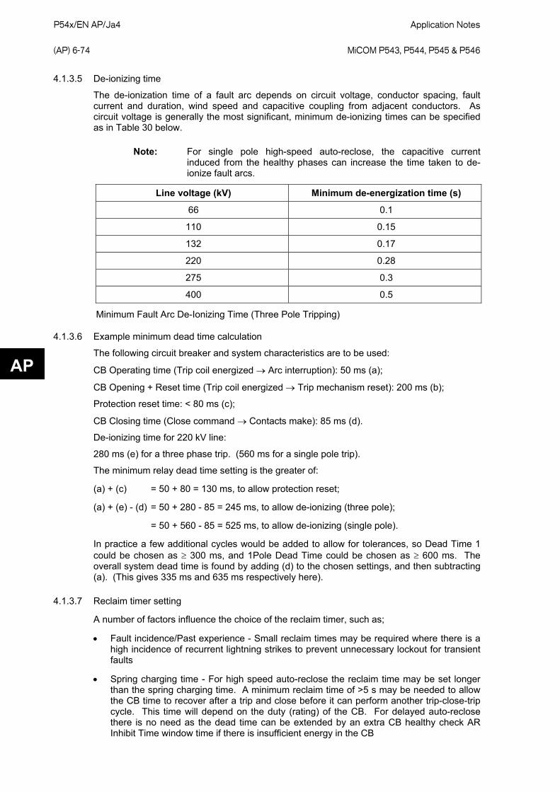
P54x/EN AP/Ja4 Application Notes (AP) 6-74
MiCOM P543, P544, P545 & P546
AP
4.1.3.5 De-ionizing time
The de-ionization time of a fault arc depends on circuit voltage, conductor spacing, fault current and duration, wind speed and capacitive coupling from adjacent conductors. As circuit voltage is generally the most significant, minimum de-ionizing times can be specified as in Table 30 below.
Note: For single pole high-speed auto-reclose, the capacitive current induced from the healthy phases can increase the time taken to de-ionize fault arcs.
Line voltage (kV) Minimum de-energization time (s)
66 0.1
110 0.15
132 0.17
220 0.28
275 0.3
400 0.5
Minimum Fault Arc De-Ionizing Time (Three Pole Tripping)
4.1.3.6 Example minimum dead time calculation
The following circuit breaker and system characteristics are to be used:
CB Operating time (Trip coil energized → Arc interruption): 50 ms (a);
CB Opening + Reset time (Trip coil energized → Trip mechanism reset): 200 ms (b);
Protection reset time: < 80 ms (c);
CB Closing time (Close command → Contacts make): 85 ms (d).
De-ionizing time for 220 kV line:
280 ms (e) for a three phase trip. (560 ms for a single pole trip).
The minimum relay dead time setting is the greater of:
(a) + (c) = 50 + 80 = 130 ms, to allow protection reset;
(a) + (e) - (d) = 50 + 280 - 85 = 245 ms, to allow de-ionizing (three pole);
= 50 + 560 - 85 = 525 ms, to allow de-ionizing (single pole).
In practice a few additional cycles would be added to allow for tolerances, so Dead Time 1 could be chosen as ≥ 300 ms, and 1Pole Dead Time could be chosen as ≥ 600 ms. The overall system dead time is found by adding (d) to the chosen settings, and then subtracting (a). (This gives 335 ms and 635 ms respectively here).
4.1.3.7 Reclaim timer setting
A number of factors influence the choice of the reclaim timer, such as;
• Fault incidence/Past experience - Small reclaim times may be required where there is a high incidence of recurrent lightning strikes to prevent unnecessary lockout for transient faults
• Spring charging time - For high speed auto-reclose the reclaim time may be set longer than the spring charging time. A minimum reclaim time of >5 s may be needed to allow the CB time to recover after a trip and close before it can perform another trip-close-trip cycle. This time will depend on the duty (rating) of the CB. For delayed auto-reclose there is no need as the dead time can be extended by an extra CB healthy check AR Inhibit Time window time if there is insufficient energy in the CB

Application Notes P54x/EN AP/Ja4 MiCOM P543, P544, P545 & P546
(AP) 6-75
AP
• Switchgear Maintenance - Excessive operation resulting from short reclaim times can mean shorter maintenance intervals
• The Reclaim Time setting is generally set greater than the tZ2 distance zone delay
4.2 Current transformer supervision
MiCOM P54x has two methods of detecting CT problems: Differential CTS and Standard CTS as detailed in the Operation Section. Both methods could be applied simultaneously and that is a significant advantage because all protection elements that would tend to operate upon CT failure will be successfully prevented from operating. The Differential CTS method should be used whenever differential protection is used, whilst the Standard CTS stabilizes all local ground protections. Therefore, to be on a safe side and cover all eventualities the recommended setting is ‘I diff + Standard CTS’ mode. Note that the ‘CTS Reset mode’ and ‘CTS Time delay’ are common for both techniques.
4.2.1 Standard CTS
The residual voltage setting, CTS Vn< Inhibit and the residual current setting, CTS Ιn> set, should be set to avoid unwanted operation during healthy system conditions. For example CTS Vn< Inhibit should be set to at least 120% of the maximum steady state residual voltage. The CTS Ιn> set will typically be set below minimum load current. The time-delayed alarm, CTS Time Delay, is generally set to 5 seconds.
Where the magnitude of residual voltage during a ground/earth fault is unpredictable, the element can be disabled to prevent protection elements being blocked during fault conditions.
Standard CTS must not be used to inhibit the operation of Current differential protection as this is a local supervision and therefore it will not be fast enough to inhibit the operation of the differential protection at the remote end.
4.2.2 Differential CTS
Phase Is1 CTS setting must be set above the phase current of the maximum load transfer expected, normally at 1.2 In. This setting defines the minimum pick-up level of the current differential protection once the current transformer supervision CTS is detected.
CTS i1> setting, once exceeded, indicates that the circuit is loaded. A default setting of 0.1 In is considered suitable for most applications, but could be lowered in case of oversized CTs.
CTS i2/i1> This setting should be in excess of the worst unbalanced load expected in the circuit under normal operation. It is recommended to read out the values of i2 and i1 in the MEASUREMENT 1 column and set the ratio above 5% of the actual ratio.
CTS i2/i1>> We strongly recommend to keep the default setting (40% In). If the ratio i2/i1 exceeds the value of this setting at only one end, the CT failure is declared.
Note: The minimum generated i2/i1 ratio will be 50% (case of one CT secondary phase lead being lost), and therefore setting of 40% is considered appropriate to guarantee sufficient operating speed.
Any of the previous methods will always block protection elements operating from derived quantities: Broken Conductor, Earth Fault and Neg Seq O/C. Other protections can be selectively blocked by customizing the PSL, gating DDB 928: CTS Block (originated by either method) or DDB 929 CTS Block Diff with the protection function logic.

P54x/EN AP/Ja4 Application Notes (AP) 6-76
MiCOM P543, P544, P545 & P546
AP
4.3 Circuit breaker condition monitoring
4.3.1 Setting the Σ Ι^ thresholds
Where overhead lines are prone to frequent faults and are protected by oil circuit breakers (OCB’s), oil changes account for a large proportion of the life cycle cost of the switchgear. Generally, oil changes are performed at a fixed interval of circuit breaker fault operations. However, this may result in premature maintenance where fault currents tend to be low, and hence oil degradation is slower than expected. The Σ Ι^ counter monitors the cumulative severity of the duty placed on the interrupter allowing a more accurate assessment of the circuit breaker condition to be made.
For OCB’s, the dielectric withstand of the oil generally decreases as a function of Σ Ι2t. This is where ‘Ι’ is the fault current broken, and ‘t’ is the arcing time within the interrupter tank (not the interrupting time). As the arcing time cannot be determined accurately, the relay would normally be set to monitor the sum of the broken current squared, by setting ‘Broken Ι^’ = 2.
For other types of circuit breaker, especially those operating on higher voltage systems, practical evidence suggests that the value of ‘Broken Ι^’ = 2 may be inappropriate. In such applications ‘Broken Ι^’ may be set lower, typically 1.4 or 1.5. An alarm in this instance may be indicative of the need for gas/vacuum interrupter HV pressure testing, for example. The setting range for ‘Broken Ι^’ is variable between 1.0 and 2.0 in 0.1 steps. It is imperative that any maintenance program must be fully compliant with the switchgear manufacturer’s instructions.
4.3.2 Setting the number of operations thresholds
Every operation of a circuit breaker results in some degree of wear for its components. Therefore, routine maintenance, such as oiling of mechanisms, may be based upon the number of operations. Suitable setting of the maintenance threshold will allow an alarm to be raised, indicating when preventative maintenance is due. Should maintenance not be carried out, the relay can be set to lockout the auto-reclose function on reaching a second operations threshold. This prevents further reclosure when the circuit breaker has not been maintained to the standard demanded by the switchgear manufacturer’s maintenance instructions.
Certain circuit breakers, such as oil circuit breakers (OCB’s) can only perform a certain number of fault interruptions before requiring maintenance attention. This is because each fault interruption causes carbonizing of the oil, degrading its dielectric properties. The maintenance alarm threshold No CB Ops. Maint. may be set to indicate the requirement for oil sampling for dielectric testing, or for more comprehensive maintenance. Again, the lockout threshold No CB Ops. Lock may be set to disable auto-reclosure when repeated further fault interruptions could not be guaranteed. This minimizes the risk of oil fires or explosion.
4.3.3 Setting the operating time thresholds
Slow CB operation is also indicative of the need for mechanism maintenance. Therefore, alarm and lockout thresholds (CB Time Maint./CB Time Lockout) are provided and are settable in the range of 5 to 500 ms. This time is set in relation to the specified interrupting time of the circuit breaker.
4.3.4 Setting the excessive fault frequency thresholds
Persistent faults will generally cause auto-reclose lockout, with subsequent maintenance attention. Intermittent faults such as clashing vegetation may repeat outside of any reclaim time, and the common cause might never be investigated. For this reason it is possible to set a frequent operations counter on the relay which allows the number of operations Fault Freq. Count over a set time period Fault Freq. Time to be monitored. A separate alarm and lockout threshold can be set.
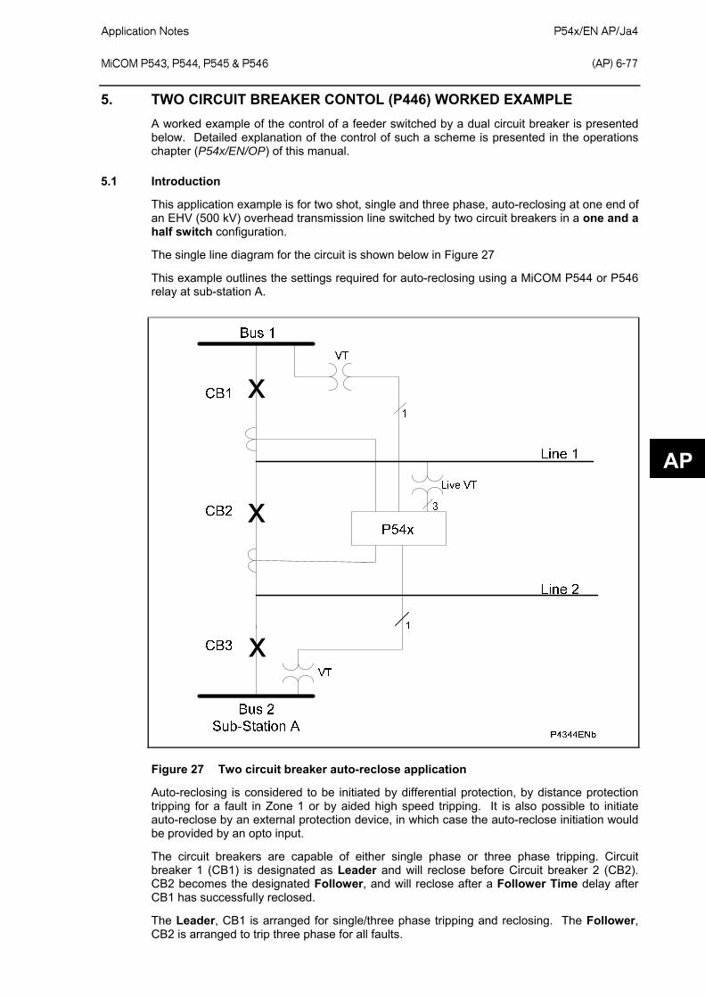
Application Notes P54x/EN AP/Ja4 MiCOM P543, P544, P545 & P546
(AP) 6-77
5. TWO CIRCUIT BREAKER CONTOL (P446) WORKED EXAMPLE A worked example of the control of a feeder switched by a dual circuit breaker is presented below. Detailed explanation of the control of such a scheme is presented in the operations chapter (P54x/EN/OP) of this manual.
5.1 Introduction
This application example is for two shot, single and three phase, auto-reclosing at one end of an EHV (500 kV) overhead transmission line switched by two circuit breakers in a one and a half switch configuration.
The single line diagram for the circuit is shown below in Figure 27
This example outlines the settings required for auto-reclosing using a MiCOM P544 or P546 relay at sub-station A.
AP
Figure 27 Two circuit breaker auto-reclose application
Auto-reclosing is considered to be initiated by differential protection, by distance protection tripping for a fault in Zone 1 or by aided high speed tripping. It is also possible to initiate auto-reclose by an external protection device, in which case the auto-reclose initiation would be provided by an opto input.
The circuit breakers are capable of either single phase or three phase tripping. Circuit breaker 1 (CB1) is designated as Leader and will reclose before Circuit breaker 2 (CB2). CB2 becomes the designated Follower, and will reclose after a Follower Time delay after CB1 has successfully reclosed.
The Leader, CB1 is arranged for single/three phase tripping and reclosing. The Follower, CB2 is arranged to trip three phase for all faults.
P54x/EN AP/Ja4 Application Notes (AP) 6-78
MiCOM P543, P544, P545 & P546
AP
For a single phase fault, CB1 will trip single phase and CB2 will trip three phase. When the fault has been cleared, CB1 will reclose single phase without any system voltage checks after the selected Single Phase AR dead time, then, after the follower time delay, CB2 will reclose three phase, subject to a synchronism check between the line and Bus 2.
For a two phase or three phase fault, both circuit breakers will trip three phase. When the fault has been cleared, CB1 will reclose three phase after the selected Three Phase AR dead time, with either live bus/dead line or live bus/live line check synchronism between the line and Bus 1. When CB1 has successfully reclosed, after the follower time delay, CB2 will reclose three phase, subject to a synchronism check between the line and Bus 2.
For live line/live bus three phase reclosing of either circuit breaker, acceptable conditions are typically:
• The phase angle difference is not greater than 20 degrees;
• The slip frequency is not greater than 0.05 Hz/s; and
• The magnitudes of both the applied line voltage and “compensated” Bus voltage are between 85% and 120% of nominal; and
• The magnitude of the difference between the applied line voltage and the “compensated” Bus voltage on either side of the circuit breaker is not greater than 10% of nominal.
It is assumed that reclosing at the remote line end will be either single phase with no system voltage checks, or three phase with live bus/live line synchronism check.
5.2 Circuit breaker status
The circuit breaker open/closed status is signalled to the auto-reclose scheme by separate type 52B auxiliary switch contacts on each circuit breaker pole (contact open when circuit breaker phase is closed, contact closed when the circuit breaker pole is open).
5.3 Voltage inputs
The voltage inputs to the auto-reclose equipment are:
• 3 phase input (3P + N, magnitude 110 V Ph-Ph, 63.5 V Ph-N) from a line VT, connected to the Line VT (main VT) input;
• 1 phase input (A-B, magnitude 110 V) from a Bus1 VT connected to the Bus1 VT (CB1 CS VT), input;
• 1 phase input (A-B, magnitude 110 V) from a Bus2 VT connected to the Bus2 VT (CB2 CS VT), input.
Under healthy system conditions each bus VT (check sync VT) input leads the A-phase to Neutral Line VT input (main VT) by 30 degrees and has voltage magnitude of 110 V (assumes settings in secondary values).
5.4 Application settings
Typical values for the principal settings and user commands related to the auto-reclosing and system voltage check functions are given below. They are presented in the order in which they appear in the menu. The hexadecimal numbers in brackets/parentheses represent the Courier cell location in the menu.
5.4.1 CB CONTROL menu:
In the CB CONTROL column, the Autoreclose Mode command (07 0B) should be activated by setting to In Service;
The data cell AR Status (07 0E) should display In Service.
The CB1 Status Input (07 11): should be set to 52B 1Pole;
The CB2 Status Input (07 80): should be set to 52B 1Pole.

Application Notes P54x/EN AP/Ja4 MiCOM P543, P544, P545 & P546
(AP) 6-79
AP
5.4.2 CONFIGURATION menu:
In the CONFIGURATION column, the following should all be set to Enabled :-
• Distance (09 0B)
• System Checks (09 23)
• Auto-Reclose (09 24)
5.4.3 CT & VT RATIOS menu:
In the CT & VT RATIOS column, the following should be set :-
• Main VT Primary (0A 01): set nominal system primary ph-ph voltage (500 kV);
• Main VT Sec’y (0A 02): set 110 V;
• CB1 CS VT Prim’y (0A 03): set nominal system primary ph-ph voltage (500 kV);
• CB1 CS VT Sec’y (0A 04): set 110 V;
• CB2 CS VT Prim’y (0A 05): set nominal system primary ph-ph voltage (500 kV);
• CB2 CS VT Sec’y (0A 06): set 110 V;
• CS Input (0A 0F): set A-N;
• CB1 CS VT PhShft (0A 21): set -30 degrees (this creates a “compensated” Bus1 phase angle normally in phase with the selected CS Input);
• CB1 CS VT Mag (0A 22): set 0.58 (this creates a “compensated” Bus1 voltage magnitude normally equal to that of the selected CS Input);
• CB2 CS VT PhShft (0A 23): set -30 degrees (this creates a “compensated” Bus2 phase angle normally in phase with the selected CS Input);
• CB2 CS VT Mag (0A 24): set 0.58 (creates a “compensated” Bus2 voltage magnitude normally equal to that of the selected CS Input);
Note: VT secondary voltage settings in this section of the menu are always set in terms of phase to phase values, even when the actual inputs are taken from phase to neutral VT terminals.
5.4.4 GROUP 1 LINE PARAMETERS menu:
In the GROUP 1 LINE PARAMETERS column, the following should be set :-
• CB1Tripping Mode (30 0C): set 1 and 3 Pole;
• CB2Tripping Mode (30 0E): set 3 Pole.
5.4.5 GROUP 1 DISTANCE menu:
• In the GROUP 1 DISTANCE column, appropriate settings should be applied and the elements enabled as per the operational requirements. Operation of the zone 1 tripping and/or the operation of the aided schemes will initiate auto-reclose.
5.4.6 GROUP 1 PHASE DIFF menu:
• In the GROUP 1 PHASE DIFF column, appropriate settings should be applied and the elements enabled as per the operational requirements. Operation of phase differential tripping will initiate auto-reclose.

P54x/EN AP/Ja4 Application Notes (AP) 6-80
MiCOM P543, P544, P545 & P546
AP
5.4.7 GROUP 1 SYSTEM CHECKS menu:
In the GROUP 1 SYSTEM CHECKS column, the following should be set :-
• Live Line (48 85): set 32 V (typical setting 50% of nominal applied voltage of selected CS Input (set to A-N in this example));
• Dead Line (48 86): set 13 V (typical setting 20% of nominal applied voltage of selected CS Input (set to A-N in this example));
• Live Bus 1 (48 87): set 32 V (typical setting 50% of “compensated” nominal applied voltage);
• Dead Bus 1 (48 88): set 13 V (typical setting 20% of “compensated” nominal applied voltage).
• Live Bus 2 (48 89): set 32 V (typical setting 50% of “compensated” nominal applied voltage);
• Dead Bus 2 (48 8 A): set 13 V (typical setting 20% of “compensated” nominal applied voltage);
• CS UV (48 8B): set 54 V (typical setting 85% of nominal applied voltage of selected CS Input (set to A-N in this example));
• CS OV (48 8C): set 76 V (typical setting 120% of nominal applied voltage of selected CS Input (set to A-N in this example));
• Sys Checks CB1 (48 8D): set Enabled;
• CB1 CS Volt. Blk (48 8E): set V< V> and Vdiff;
• CB1 CS1 Status (48 8F): set Enabled;
• CB1 CS1 Angle (48 90): set 20 degree;
• CB1 CS1 Vdiff (48 91): set 6.5 V (typical setting 10% of nominal applied voltage of selected CS Input (set to A-N in this example));
• CB1 CS1 SlipCtrl (48 92): set Enabled;
• CB1 CS1 SlipFreq (48 93): set 0.05Hz;
• CB1 CS2 Status (48 94): set Disabled;
• Sys Checks CB2 (48 9B): set Enabled;
• CB2 CS Volt. Blk (48 9C): set V< V> and Vdiff;
• CB2 CS1 Status (48 9D): set Enabled;
• CB2 CS1 Angle (48 9E): set 20 degrees;
• CB2 CS1 Vdiff (48 9F): set 6.5 V (typical setting 10% of nominal applied voltage of selected CS Input (set to A-N in this example));
• CB2 CS1 SlipCtrl (48 A0): set Enable;
• CB2 CS1 SlipFreq (48 A1): set 0.05Hz;
• CB2 CS2 Status (48 94): set Disabled;

Application Notes P54x/EN AP/Ja4 MiCOM P543, P544, P545 & P546
(AP) 6-81
AP
5.4.8 GROUP 1 AUTORECLOSE menu:
In the GROUP 1 AUTORECLOSE column, the following should be set :-
• Num CBs (49 50): set Both CB1&CB2;
• Lead/Foll ARMode (49 53): set L 1/3P, F 3P;
• Leader Select By (49 55): set Menu;
• Select Leader (49 56): set Sel Leader CB1;
• BF if LFail Cls (49 57): set Enabled;
• AR Shots (49 59): set 2;
• Multi Phase AR (49 5C): set Allow Autoclose;
• Discrim Time (49 5D): set 0.5 sec (set as per application requirements);
• CB IS Time (49 60): set 5 sec (this requires the circuit breaker to have been in the closed position for at least 5 seconds before fault occurrence will enable auto-reclose initiation. It is designed to prevent auto-reclosure for a fault immediately after manual circuit breaker closure (switch on to fault));
• CB IS Memory Time (49 61): set 0.5 sec;
• DT Start by Prot (49 62): set Protection Reset (measured dead time starts when protection resets);
• 3PDTStart WhenLD (49 63): set Disabled;
• DTStart by CB Op (49 64): set Disabled;
• SP AR Dead Time (49 67): set 0.5 sec (typical);
• 3P AR DT Shot 1 (49 68): set 0.3 sec (or as per application requirements and considerations at circuit breaker location);
• 3P AR DT Shot 2 (49 68): set 60 sec (or as per application requirements and considerations at the circuit breaker location);
• Follower Time (49 6C): set 5 se” (typical);
• SPAR ReclaimTime (49 6D): set 180 sec (or as required to suit circuit breaker duty cycle);
• 3P AR ReclaimTime (49 6E): set 180 sec (or as required to suit circuit breaker duty cycle);
• AR CBHealthyTime (49 6F): set 0.3 sec;
• AR CheckSyncTime (49 70): set 0.3 sec;
• Z1 AR (49 72): set Initiate AR;
• Diff AR (49 73): set Initiate AR;
• Dist Aided AR (49 74): set Initiate AR;
• All other protection inputs (Z2T AR (49 72) onwards) : set Block AR;
• CB1L SC all (49 A6): set Enabled;
• CB1L SC Shot 1 (49 A7): set Enabled;
• CB1L SC ClsNoDly (49 A8): set Disabled;
• CB1L SC CS1 (49 A9): set Enabled;
• CB1L SC CS2 (49 AA): set Disabled;

P54x/EN AP/Ja4 Application Notes (AP) 6-82
MiCOM P543, P544, P545 & P546
• CB1L SC DLLB (49 AB): set Enabled;
• CB1L SC LLDB (49 AC): set Disabled;
• CB1L SC DLDB (49 AD): set Disabled;
• CB2F SC all (49 BD): set Enabled;
• CB2F SC Shot 1 (49 BE): set Enabled;
• CB2F SC CS1 (49 BF): set Enabled;
• CB2F SC CS2 (49 C0): set Disabled;
• CB2F SC DLLB (49 C1): set Disabled;
• CB2F SC LLDB (49 C2): set Disabled;
• CB2F SC DLDB (49 C3): set Disabled.
5.5 PSL (Programmable Scheme Logic) MAPPING
The PSL mapping of some of the opto inputs and relay outputs for this application example are shown below for guidance.
AP
In order to test the application example, as well as applying appropriate current and voltage connections, the settings, and the PSL, it will be necessary to employ some secondary test equipment capable of mimicking the circuit breaker status.
For any specific application, the Application Engineer must analyze the particular power systems to determine the appropriate settings and PSL mappings.

Application Notes P54x/EN AP/Ja4 MiCOM P543, P544, P545 & P546
(AP) 6-83
AP
6. CURRENT TRANSFORMER REQUIREMENTS
6.1 Recommended CT classes (British and IEC)
Class X current transformers with a knee point voltage greater or equal than that calculated can be used.
Class 5P protection CTs can be used, noting that the knee point voltage equivalent these offer can be approximated from:
Vk = (VA x ALF)/In + (RCT x ALF x In)
Where:
VA = Voltampere burden rating
ALF = Accuracy limit factor
In = CT nominal secondary current
6.2 Current differential requirements
For accuracy, class X or class 5P current transformers (CTs) are strongly recommended. The knee point voltage of the CTs should comply with the minimum requirements of the formulae shown below.
Vk ≥ K. In (Rct + 2 RL)
Where:
Vk = Required IEC knee point voltage
K = Dimensioning factor
In = CT nominal secondary current
Rct = CT resistance
RL = One-way lead impedance from CT to relay
K is a constant depending on:
If = Maximum value of through fault current for stability (multiple of In)
X/R = Primary system X/R ratio
K is determined as follows:
For relays set at Is1 = 20%, Is2 = 2 In, k1 = 30%, k2 = 150%:
K must be the highest of:
K ≥ 40 + (0.07 x (If x X/R))
Or
K ≥ 65
This is valid for (If x X/R) ≤ 1000
For higher (If x X/R) up to 1600:
K = 107
For relays set at Is1 = 20%, Is2 = 2 In, k1 = 30%, k2 = 100%:
K must be the highest of:
K ≥ 40 + (0.35 x (If x X/R))

P54x/EN AP/Ja4 Application Notes (AP) 6-84
MiCOM P543, P544, P545 & P546
AP
Or
K ≥ 65
This is valid for (If x X/R) ≤ 600
For higher (If x X/R) up to 1600:
K = 256
6.3 Zone 1 reach point accuracy (RPA)
Vk ≥ KRPA x IF Z1 x (1+ X/R). (RCT + RL)
Where:
Vk = Required CT knee point voltage (volts)
KRPA = Fixed dimensioning factor = always 0.6
IF Z1 = Max. secondary phase fault current at Zone 1 reach point (A)
X/R = Primary system reactance/resistance ratio
RCT = CT secondary winding resistance (Ω)
RL = Single lead resistance from CT to relay (Ω)
6.4 Zone 1 close-up fault operation
An additional calculation must be performed for all cables, and any lines where the source impedance ratio might be less than SIR = 2.
Vk ≥ Kmax x IF max x (RCT + RL)
Where:
Kmax = Fixed dimensioning factor = always 1.4
IF max = Max. secondary phase fault current (A).
Then, the highest of the two calculated knee points must be used. Note that it is not necessary to repeat the calculation for earth faults, as the phase reach calculation (3ϕ) is the worst-case for CT dimensioning.
6.5 Time delayed distance zones
When a time delayed distance zone is being used, there is no need to calculate the required Vk separately. This is due to the employed time delay (usually more than 3 times the primary time constant for a fault at the remote bus of the protected feeder), which overrides the transient conditions. When it is insisted to do some calculations for the time delayed distance zone, then we should use the following equation
Vk > If (RCT + RL)
Where If is the current for a fault at the remote bus of the protected feeder (in other words, the through fault current for the current differential function)
6.6 Determining Vk for an IEEE “C" class CT
Where American/IEEE standards are used to specify CTs, the C class voltage rating can be checked to determine the equivalent Vk (knee point voltage according to IEC). The equivalence formula is:
Vk = [(C rating in volts) x 1.05] + [100 x RCT]

Application Notes P54x/EN AP/Ja4 MiCOM P543, P544, P545 & P546
(AP) 6-85
AP
6.7 Worked example for CT requirements
The Power system and the line parameters (Line length: 100 km) as given in section 3.2 is used here to calculate CT requirements.
6.7.1 Important notes to be considered
• Current differential – Both If and X/R are to be calculated for a through fault
• Distance Zone1 reach point case – Both If and X/R are to be calculated for a fault at Zone1 reach point
• For calculating the CT requirements, the bus bar short time symmetrical fault rating shall be considered as the bus fault level.
• When there are only indicative X/Rs available, then the circuit breaker’s dc breaking capacity shall be used to arrive at the primary time constant (and hence the primary system X/R). The derivation shall be obtained from the circuit breaker manufacturer; practical primary time constants arrived in such a way vary between 50 ms (applicable for 66 kV and 132 kV breakers) and 120 ms (applicable for 220 kV and 400 kV breakers). 150 ms is a practical figure for generator circuit breakers.
6.7.2 System data
In the following example, the following parameters have been considered for the CT calculations:
System voltage - 230 kV
System frequency - 50 Hz
System grounding - solid
Single circuit operation between Green Valley and Blue River
CT ratio - 1200/1
Line length - 100 kms
Line positive sequence impedance Z1 = 0.089 + j 0.476 ohm / km
Bus fault level - 40 kA
Primary time constant = 120 ms
6.7.3 Calculation of Primary X/R
Primary X/R till the Green Valley bus = 2 * pi * f * primary time constant in s
= 2 * pi * 50 * 0.12
Primary X/R till the bus = 37.7
6.7.4 Calculation of Source Impedance Zs
Source Impedance Zs = 230 kV / (1.732 * 40 kA) = 3.32 ohms
Source angle = tan-1 (X/R)
= tan-1 (37.7) = 88.48 deg
Hence, Zs = 0.088 + j 3.317 ohms

P54x/EN AP/Ja4 Application Notes (AP) 6-86
MiCOM P543, P544, P545 & P546
AP
6.7.5 Calculation of full line impedance (full 100 kms)
Z1 = 0.089 + j 0.476 ohm / km
ZL = 8.9 + j 47.6 ohms
ZL = 48.42 ohms with an angle 79.4 deg
6.7.6 Calculation of total impedance till remote bus bar
ZT = Zs + ZL = 8.988 + j 50.917 ohms
= 51.7 ohms with an angle of 80 deg
6.7.7 Calculation of through fault X/R
X/R thro = 50.917 / 8.988
= 5.66
6.7.8 Calculation of through fault If
If thro = 230kV / (1.732 * 51.7 )
= 2568.5 A primary
= 2.14 A (secondary)
6.7.9 Calculation of line impedance till Zone1 reach point (80kms)
Zzone1 = 0.8 * ZL = 7.12 + j 38.08 ohms
= 38.73 ohms with an angle of 79.4 deg
6.7.10 Calculation of total impedance till Zone1 reach point
ZTzone1 = Zs + Zzone1
= 7.208 + j 41.397 ohms
= 42.019 ohms with an angle of 80 deg
6.7.11 Calculation of X/R till Zone1 reach point
X/R zone1 = 41.397 / 7.208
= 5.74
6.7.12 Calculation of fault current till Zone1 reach point
If zone1 = 230 kV / (1.732 * 42.019)
= 3160.34 A (primary) = 2.63 A (secondary)

Application Notes P54x/EN AP/Ja4 MiCOM P543, P544, P545 & P546
(AP) 6-87
AP
6.7.13 CT Vk for Current differential protection
If thro * X/R thro = 2.14 * 5.66
= 12.11
The appropriate equation for K and Vk to be is used from section 6.2
K > 40 + (0.07 * 12.11) OR K > 65
K > 40.8 OR K > 65
Hence K = 65
Vk ≥ K. In (Rct + 2 RL)
Vk > 65 (RCT + 2 RL)
6.7.14 CT Vk for distance Zone1 reach point
Vk ≥ KRPA x IF z1 x (1+ X/R). (RCT + RL) -- From section 6.3
Vk > 0.6 * 2.63 * (1+5.74) * (RCT+RL)
Vk > 10.65 (RCT + RL)
6.7.15 CT Vk for distance Zone1 close-up fault
SIR = Zs / Zzone1 = 3.32 / 38.73 is less than 2; so we need to do this Vk calculation
Close-up fault current = 40kA (primary) = 33.33 A (secondary)
Vk ≥ Kmax x IF max x (RCT + RL) -- From section 6.4
Vk > 1.4 * 33.33 * ( RCT + RL)
Vk > 46.67 (RCT + RL)
6.7.16 CT Vk for distance time delayed zones
Vk > If (RCT + RL) -- From section 6.5
Vk > If thro * (RCT + RL)
Vk > 2.14 (RCT + RL)
6.7.17 Vk to be considered
Using the above sections, the different Vk requirements are to be calculated for all the functions that will be enabled, or that will be brought into operation. Then the highest Vk shall be considered for the CT design.

P54x/EN AP/Ja4 Application Notes (AP) 6-88
MiCOM P543, P544, P545 & P546
AP
7. HIGH BREAK OUTPUT CONTACTS The high break contacts allow the elimination of auxiliary relays. This in turn helps in the provision of cost effective solutions, minimizing space, wiring, commissioning time, etc..
According to the model selected, in addition to standard output relay boards, one or two ‘high break’ output relay boards can be fitted. Each houses four normally open output contacts suitable for breaking loads higher than can be broken with the standard contacts. The performance and possible application scenarios of these contacts are described in the Technical Data (TD) and Firmware Design (FD) chapters of this manual.
8. AUXILIARY SUPPLY FUSE RATING In the Safety section of this manual, the maximum allowable fuse rating of 16 A is quoted. To allow time grading with fuses upstream, a lower fuselink current rating is often preferable. Use of standard ratings of between 6 A and 16 A is recommended. Low voltage fuselinks, rated at 250 V minimum and compliant with IEC 60269-2 general application type gG are acceptable, with high rupturing capacity. This gives equivalent characteristics to HRC "red spot" fuses type NIT/TIA often specified historically.
The table below recommends advisory limits on relays connected per fused spur. This applies to MiCOM Px40 series devices with hardware suffix C and higher, as these have inrush current limitation on switch-on, to conserve the fuse-link.
Maximum number of MiCOM Px40 relays recommended per fuse
Battery nominal voltage 6 A 10 A fuse 15 or 16 A fuse Fuse rating > 16 A
24 to 54 V 2 4 6 Not permitted
60 to 125 V 4 8 12 Not permitted
138 to 250 V 6 10 16 Not permitted
Alternatively, miniature circuit breakers (MCB) may be used to protect the auxiliary supply circuits.

Programmable Logic P54x/EN PL/Ba4 MiCOM P543, P544, P545 & P546
PL PROGRAMMABLE LOGIC
Date: 16th March 2009 Hardware suffix: K Software version:
45 (P543/4/5/6 without Distance) 55 (P543/4/5/6 with Distance)
Connection diagrams:
10P54302 (SH 1 to 2) 10P54303 (SH 1 to 2)
10P54400 10P54404 (SH 1 to 2) 10P54405 (SH 1 to 2)
10P54502 (SH 1 to 2) 10P54503 (SH 1 to 2)
10P54600 10P54604 (SH 1 to 2) 10P54605 (SH 1 to 2) 10P54606 (SH 1 to 2)

P54x/EN PL/Ba4 Programmable Logic
MiCOM P543, P544, P545 & P546
PL

Programmable Logic P54x/EN PL/Ba4 MiCOM P543, P544, P545 & P546
(PL) 7-1
PL
CONTENTS
(PL) 7-
1. PROGRAMMABLE LOGIC 5 1.1 Overview 5 1.2 MiCOM S1 Studio Px40 PSL editor 5 1.3 How to use MiCOM Px40 PSL editor 6 1.4 Warnings 6 1.5 Toolbar and commands 7 1.5.1 Standard tools 7 1.5.2 Alignment tools 7 1.5.3 Drawing tools 7 1.5.4 Nudge tools 7 1.5.5 Rotation tools 7 1.5.6 Structure tools 7 1.5.7 Zoom and pan tools 7 1.5.8 Logic symbols 7 1.6 PSL logic signals properties 9 1.6.1 Link properties 9 1.6.2 Opto signal properties 10 1.6.3 Input signal properties 10 1.6.4 Output signal properties 10 1.6.5 GOOSE input signal properties 10 1.6.6 GOOSE output signal properties 11 1.6.7 Control in signal properties 11 1.6.8 InterMiCOM In commands properties 11 1.6.9 Function key properties 12 1.6.10 Fault recorder trigger properties 12 1.6.11 LED signal properties 12 1.6.12 Contact signal properties 12 1.6.13 LED conditioner properties 13 1.6.14 Contact conditioner properties 13 1.6.15 Timer properties 14 1.6.16 Gate properties 14 1.6.17 SR programmable gate properties 15 1.7 Description of logic nodes 16 1.8 Factory default programmable scheme logic 54 1.9 Logic input mappings 54 1.10 Standard relay output contact mappings 57 1.11 Optional high break relay output contact mappings 60
P54x/EN PL/Ba4 Programmable Logic
(PL) 7-2
MiCOM P543, P544, P545 & P546
PL
1.12 Programmable LED output mappings 63 1.13 Fault recorder start mappings 66 1.14 PSL DATA column 66
MICOM P543 WITH DISTANCE PROGRAMMABLE SCHEME LOGIC 67 Output Input Mappings 67 Output Contacts 68 Output Contacts 69 LEDs 70
MICOM P543 WITHOUT DISTANCE PROGRAMMABLE SCHEME LOGIC 80 Output Input Mappings 80 Output Contacts 81 Output Contacts 82 LEDs 83
MICOM P544 WITH DISTANCE PROGRAMMABLE SCHEME LOGIC 92 Output Input Mappings 92 Output Contacts 93 Output Contacts 94 Output Contacts 95
MICOM P544 WITHOUT DISTANCE PROGRAMMABLE SCHEME LOGIC 105 Output Input Mappings 105 Output Contacts 106 Output Contacts 107 Output Contacts 108 LEDs 109
MICOM P545 WITH DISTANCE PROGRAMMABLE SCHEME LOGIC 118 Output Input Mappings 118 Output Contacts 119 Output Contacts 120 Output Contacts 121 LEDs 122
MICOM P545 WITHOUT DISTANCE PROGRAMMABLE SCHEME LOGIC 132 Output Input Mappings 132 Output Contacts 133 Output Contacts 134 Output Contacts 135 LEDs 136
MICOM P546 WITH DISTANCE PROGRAMMABLE SCHEME LOGIC 145 Output Input Mappings 145 Output Contacts 146

Programmable Logic P54x/EN PL/Ba4 MiCOM P543, P544, P545 & P546
(PL) 7-3
PL
Output Contacts 147 Output Contacts 148 Output Contacts 149 LEDs 158
MICOM P546 WITHOUT DISTANCE PROGRAMMABLE SCHEME LOGIC 159 Output Input Mappings 159 Output Contacts 160 Output Contacts 161 Output Contacts 162 Output Contacts 163 LEDs 172

P54x/EN PL/Ba4 Programmable Logic
(PL) 7-4
MiCOM P543, P544, P545 & P546
PL

Programmable Logic P54x/EN PL/Ba4 MiCOM P543, P544, P545 & P546
(PL) 7-5
PL
1. PROGRAMMABLE LOGIC
1.1 Overview
The purpose of the programmable scheme logic (PSL) is to allow the relay user to configure an individual protection scheme to suit their own particular application. This is achieved through the use of programmable logic gates and delay timers.
The input to the PSL is any combination of the status of opto inputs. It is also used to assign the mapping of functions to the opto inputs and output contacts, the outputs of the protection elements, e.g. protection starts and trips, and the outputs of the fixed protection scheme logic. The fixed scheme logic provides the relay’s standard protection schemes. The PSL itself consists of software logic gates and timers. The logic gates can be programmed to perform a range of different logic functions and can accept any number of inputs. The timers are used either to create a programmable delay, and/or to condition the logic outputs, e.g. to create a pulse of fixed duration on the output regardless of the length of the pulse on the input. The outputs of the PSL are the LEDs on the front panel of the relay and the output contacts at the rear.
The execution of the PSL logic is event driven; the logic is processed whenever any of its inputs change, for example as a result of a change in one of the digital input signals or a trip output from a protection element. Also, only the part of the PSL logic that is affected by the particular input change that has occurred is processed. This reduces the amount of processing time that is used by the PSL; even with large, complex PSL schemes the relay trip time will not lengthen.
This system provides flexibility for the user to create their own scheme logic design. However, it also means that the PSL can be configured into a very complex system; hence setting of the PSL is implemented through the PC support package MiCOM S1 Studio.
1.2 MiCOM S1 Studio Px40 PSL editor
To access the Px40 PSL Editor menu click on
The PSL Editor module enables you to connect to any MiCOM device front port, retrieve and edit its Programmable Scheme Logic files and send the modified file back to a MiCOM Px40 device.
P54x/EN PL/Ba4 Programmable Logic
(PL) 7-6
MiCOM P543, P544, P545 & P546
PL
1.3 How to use MiCOM Px40 PSL editor
With the MiCOM Px40 PSL Module you can:
• Start a new PSL diagram
• Extract a PSL file from a MiCOM Px40 IED
• Open a diagram from a PSL file
• Add logic components to a PSL file
• Move components in a PSL file
• Edit link of a PSL file
• Add link to a PSL file
• Highlight path in a PSL file
• Use a conditioner output to control logic
• Download PSL file to a MiCOM Px40 IED
• Print PSL files
For a detailed discussion on how to use these functions, please refer to MiCOM S1 Studio Users Manual.
1.4 Warnings
Before the scheme is sent to the relay checks are done. Various warning messages may be displayed as a result of these checks.
The Editor first reads in the model number of the connected relay, and then compares it with the stored model number. A "wildcard" comparison is employed. If a model mismatch occurs then a warning will be generated before sending commences. Both the stored model number and that read-in from the relay are displayed along with the warning; the onus is on you to decide if the settings to be sent are compatible with the connected relay. Wrongly ignoring the warning could lead to undesired behavior in the relay.
If there are any potential problems of an obvious nature then a list will be generated. The types of potential problems that the program attempts to detect are:
• One or more gates, LED signals, contact signals, and/or timers have their outputs linked directly back to their inputs. An erroneous link of this sort could lock up the relay, or cause other more subtle problems to arise.
• Inputs to Trigger (ITT) exceeds the number of inputs. A programmable gate has its ITT value set to greater than the number of actual inputs; the gate can never activate. Note that there is no lower ITT value check. A 0-value does not generate a warning.
• Too many gates. There is a theoretical upper limit of 256 gates in a scheme, but the practical limit is determined by the complexity of the logic. In practice the scheme would have to be very complex, and this error is unlikely to occur.
• Too many links. There is no fixed upper limit to the number of links in a scheme. However, as with the maximum number of gates, the practical limit is determined by the complexity of the logic. In practice the scheme would have to be very complex, and this error is unlikely to occur.

Programmable Logic P54x/EN PL/Ba4 MiCOM P543, P544, P545 & P546
(PL) 7-7
PL
1.5 Toolbar and commands
There are a number of toolbars available for easy navigation and editing of PSL.
1.5.1 Standard tools
• For file management and printing.
1.5.2 Alignment tools
• To snap logic elements into horizontally or vertically aligned groupings.
1.5.3 Drawing tools
• To add text comments and other annotations, for easier reading of PSL schemes.
1.5.4 Nudge tools
• To move logic elements.
1.5.5 Rotation tools
• Tools to spin, mirror and flip.
1.5.6 Structure tools
• To change the stacking order of logic components.
1.5.7 Zoom and pan tools
• For scaling the displayed screen size, viewing the entire PSL, or zooming to a selection.
1.5.8 Logic symbols
This toolbar provides icons to place each type of logic element into the scheme diagram. Not all elements are available in all devices. Icons will only be displayed for those elements available in the selected device.
Link
Create a link between two logic symbols.

P54x/EN PL/Ba4 Programmable Logic
(PL) 7-8
MiCOM P543, P544, P545 & P546
PL
Opto Signal
Create an opto signal.
Input Signal
Create an input signal.
Output Signal
Create an output signal.
GOOSE In
Create an input signal to logic to receive a GOOSE message transmitted from another IED. Used in either UCA2.0 or IEC 61850 GOOSE applications only. GOOSE Out
Create an output signal from logic to transmit a GOOSE message to another IED. Used in either UCA2.0 or IEC 61850 GOOSE applications only. Control In
Create an input signal to logic that can be operated from an external command.
InterMiCOM In
Create an input signal to logic to receive an InterMiCOM command transmitted from another IED.
InterMiCOM Out
Create an output signal from logic to transmit an InterMiCOM command to another IED. Function Key
Create a function key input signal.
Trigger Signal
Create a fault record trigger.
LED Signal
Create an LED input signal that repeats the status of tri-color LED.
Contact Signal
Create a contact signal.
LED Conditioner
Create an LED conditioner.
Contact Conditioner
Create a contact conditioner.
Timer
Create a timer.
AND Gate

Programmable Logic P54x/EN PL/Ba4 MiCOM P543, P544, P545 & P546
(PL) 7-9
PL
Create an AND Gate.
OR Gate
Create an OR Gate.
Programmable Gate
Create a programmable gate.
1.6 PSL logic signals properties
The logic signal toolbar is used for the selection of logic signals.
Performing a right-mouse click on any logic signal will open a context sensitive menu and one of the options for certain logic elements is the Properties command. Selecting the Properties option will open a Component Properties window, the format of which will vary according to the logic signal selected.
Properties of each logic signal, including the Component Properties windows, are shown in the following sub-sections:
Signal Properties Menu
The Signals List tab is used for the selection of logic signals.
The signals listed will be appropriate to the type of logic symbol being added to the diagram. They will be of one of the following types:
1.6.1 Link properties
Links form the logical link between the output of a signal, gate or condition and the input to any element.
Any link that is connected to the input of a gate can be inverted via its properties window. An inverted link is indicated with a “bubble” on the input to the gate. It is not possible to invert a link that is not connected to the input of a gate.
Rules for Linking Symbols
Links can only be started from the output of a signal, gate, or conditioner, and can only be ended on an input to any element.
Since signals can only be either an input or an output then the concept is somewhat different. In order to follow the convention adopted for gates and conditioners, input signals are connected from the left and output signals to the right. The Editor will automatically enforce this convention.
A link attempt will be refused where one or more rules would otherwise be broken. A link will be refused for the following reasons:
• An attempt to connect to a signal that is already driven. The cause of the refusal may not be obvious, since the signal symbol may appear elsewhere in the diagram. Use “Highlight a Path” to find the other signal.
• An attempt is made to repeat a link between two symbols. The cause of the refusal may not be obvious, since the existing link may be represented elsewhere in the diagram.

P54x/EN PL/Ba4 Programmable Logic
(PL) 7-10
MiCOM P543, P544, P545 & P546
PL
1.6.2 Opto signal properties
Opto Signal
Each opto input can be selected and used for programming in PSL. Activation of the opto input will drive an associated DDB signal.
For example activating opto input L1 will assert DDB 032 in the PSL.
1.6.3 Input signal properties
Input Signal
Relay logic functions provide logic output signals that can be used for programming in PSL. Depending on the relay functionality, operation of an active relay function will drive an associated DDB signal in PSL.
For example DDB 671 will be asserted in the PSL should the active earth fault 1, stage 1 protection operate/trip.
1.6.4 Output signal properties
Output Signal
Relay logic functions provide logic input signals that can be used for programming in PSL. Depending on the relay functionality, activation of the output signal will drive an associated DDB signal in PSL and cause an associated response to the relay function
For example, if DDB 409 is asserted in the PSL, it will block the sensitive earth function stage 1 timer.
1.6.5 GOOSE input signal properties
GOOSE In
The Programmable Scheme Logic interfaces with the GOOSE Scheme Logic (see S1 users manual) by means of 32 Virtual inputs. The Virtual Inputs can be used in much the same way as the Opto Input signals.
The logic that drives each of the Virtual Inputs is contained within the relay’s GOOSE Scheme Logic file. It is possible to map any number of bit-pairs, from any subscribed device, using logic gates onto a Virtual Input (see S1 Users manual for more details).
For example DDB 224 will be asserted in PSL should virtual input 1 operate.

Programmable Logic P54x/EN PL/Ba4 MiCOM P543, P544, P545 & P546
(PL) 7-11
PL
1.6.6 GOOSE output signal properties
GOOSE Out
The Programmable Scheme Logic interfaces with the GOOSE Scheme Logic by means of 32 Virtual outputs.
It is possible to map virtual outputs to bit-pairs for transmitting to any subscribed devices (see S1 Users manual for more details).
For example if DDB 256 is asserted in PSL, Virtual Output 32 and its associated mappings will operate.
1.6.7 Control in signal properties
Control In
There are 32 control inputs which can be activated via the relay menu, ‘hotkeys’ or via rear communications. Depending on the programmed setting i.e. latched or pulsed, an associated DDB signal will be activated in PSL when a control input is operated.
For example operate control input 1 to assert DDB 192 in the PSL.
1.6.8 InterMiCOM In commands properties
InterMiCOM Out
There are 16 InterMiCOM outputs that could be selected and use for teleprotection, remote commands, etc. “InterMiCOM Out” is a send command to a remote end that could be mapped to any logic output or opto input. This will be transmitted to the remote end as corresponding “InterMiCOM In” command
InterMiCOM In
There are 16 InterMiCOM inputs that could be selected and use for teleprotection, remote commands, etc. “InterMiCOM In” is a received signal from remote end that could be mapped to a selected output relay or logic input.
Example
Relay End A
At end A, InterMiCOM Output 1 is mapped to the command indication “Clear Statistics” (issued at end A)
Relay End B
At end B, InterMiCOM Input 1 is mapped to the command “Clear Statistics”
Upon receive of IM64 1 from relay at end A, the relay at end B will reset its statistics.
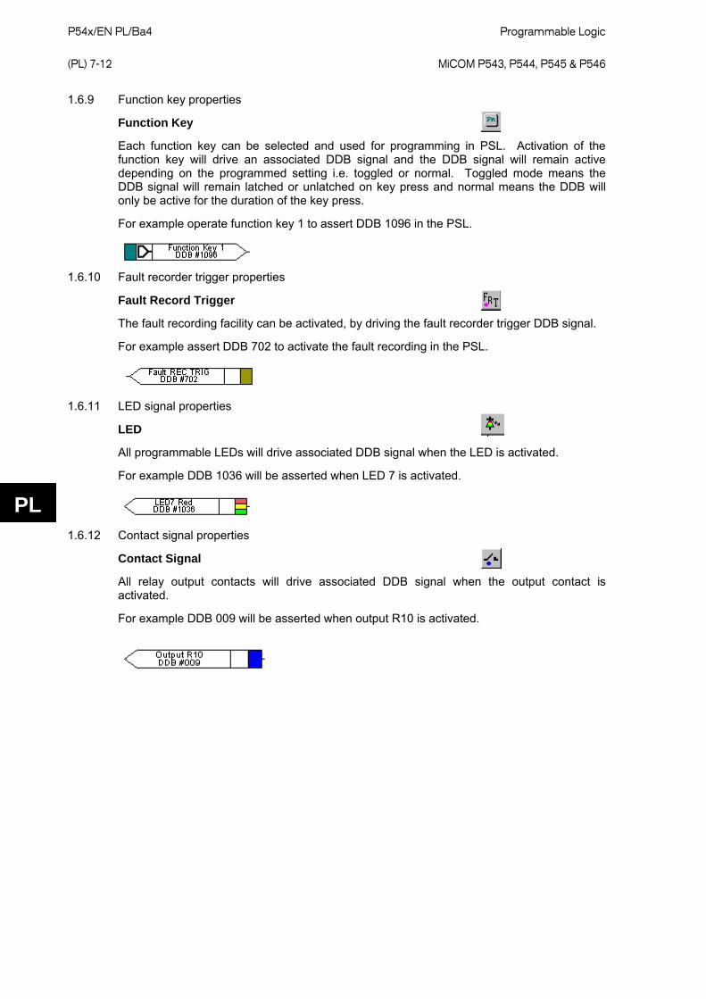
P54x/EN PL/Ba4 Programmable Logic
(PL) 7-12
MiCOM P543, P544, P545 & P546
PL
1.6.9 Function key properties
Function Key
Each function key can be selected and used for programming in PSL. Activation of the function key will drive an associated DDB signal and the DDB signal will remain active depending on the programmed setting i.e. toggled or normal. Toggled mode means the DDB signal will remain latched or unlatched on key press and normal means the DDB will only be active for the duration of the key press.
For example operate function key 1 to assert DDB 1096 in the PSL.
1.6.10 Fault recorder trigger properties
Fault Record Trigger
The fault recording facility can be activated, by driving the fault recorder trigger DDB signal.
For example assert DDB 702 to activate the fault recording in the PSL.
1.6.11 LED signal properties
LED
All programmable LEDs will drive associated DDB signal when the LED is activated.
For example DDB 1036 will be asserted when LED 7 is activated.
1.6.12 Contact signal properties
Contact Signal
All relay output contacts will drive associated DDB signal when the output contact is activated.
For example DDB 009 will be asserted when output R10 is activated.

Programmable Logic P54x/EN PL/Ba4 MiCOM P543, P544, P545 & P546
(PL) 7-13
PL
1.6.13 LED conditioner properties
LED Conditioner
1. Select the LED name from the list (only shown when inserting a new symbol).
2. Configure the LED output to be Red, Yellow or Green.
Configure a Green LED by driving the Green DDB input.
Configure a RED LED by driving the RED DDB input.
Configure a Yellow LED by driving the RED and GREEN DDB inputs simultaneously.
3. Configure the LED output to be latching or non-latching.
1.6.14 Contact conditioner properties
Each contact can be conditioned with an associated timer that can be selected for pick up, drop off, dwell, pulse, pick-up/drop-off, straight-through, or latching operation. “Straight-through” means it is not conditioned in any way whereas “latching” is used to create a sealed-in or lockout type function.
4. Select the contact name from the Contact Name list (only shown when inserting a new symbol).
5. Choose the conditioner type required in the Mode tick list.
6. Set the Pick-up Time (in milliseconds), if required.
7. Set the Drop-off Time (in milliseconds), if required.

P54x/EN PL/Ba4 Programmable Logic
(PL) 7-14
MiCOM P543, P544, P545 & P546
PL
1.6.15 Timer properties
Each timer can be selected for pick up, drop off, dwell, pulse or pick-up/drop-off operation.
1. Choose the operation mode from the Timer Mode tick list.
2. Set the Pick-up Time (in milliseconds), if required.
3. Set the Drop-off Time (in milliseconds), if required.
1.6.16 Gate properties or
A Gate may be an AND, OR, or programmable gate.
An AND gate requires that all inputs are TRUE for the output to be TRUE.
An OR gate requires that one or more input is TRUE for the output to be TRUE.
A Programmable gate requires that the number of inputs that are TRUE is equal to or
greater than its ‘Inputs to Trigger’ setting for the output to be TRUE.

Programmable Logic P54x/EN PL/Ba4 MiCOM P543, P544, P545 & P546
(PL) 7-15
PL
1. Select the Gate type AND, OR, or Programmable.
2. Set the number of inputs to trigger when Programmable is selected.
3. Select if the output of the gate should be inverted using the Invert Output check box. An inverted output is indicated with a "bubble" on the gate output.
1.6.17 SR programmable gate properties
A Programmable SR gate can be selected to operate with the following three latch properties:
S input R input O - Standard O – Set input dominant
O – Rest input dominant
0 0 0 0 0
0 1 0 0 0
1 0 1 1 1
1 1 0 1 1
Select if the output of the gate should be inverted using the Invert Output check box. An inverted output is indicated with a "bubble" on the gate output.
P54x/EN PL/Ba4 Programmable Logic
(PL) 7-16
MiCOM P543, P544, P545 & P546
PL
1.7 Description of logic nodes
Note: Where applicable. Not all nodes appear in every product variant.
DDB no. English text Source Description
0 Output R1 Output Conditioner Assignment of signal to drive output Relay 1
31 Output R32 Output Conditioner Assignment of signal to drive output Relay 32
32 Input L1 Opto Input From opto input 1 - when opto energized
55 Input L16 Opto Input From opto input 24 - when opto energized
63 Input L24 Opto Input From opto input 32 - when opto energized
64 to 95 Not used
96 IM64 Ch1 Input 1 IM64 IM64 Ch1 input 1 - is driven by a message from the remote line end
103 IM64 Ch1 Input 8 IM64 IM64 Ch1 input 8 - is driven by a message from the remote line end
104 IM64 Ch2 Input 1 IM64 IM64 Ch2 input 1 - is driven by a message from the remote line end
111 IM64 Ch2 Input 8 IM64 IM64 Ch2 input 8 - is driven by a message from the remote line end
112 IM64 Ch1 Output 1 PSL IM64 Ch1 output 1 - mapping what will be sent to the remote line end
119 IM64 Ch1 Output 8 PSL IM64 Ch1 output 8 - mapping what will be sent to the remote line end
120 IM64 Ch2 Output 1 PSL IM64 Ch2 output 1 - mapping what will be sent to the remote line end
127 IM64 Ch2 Output 8 PSL IM64 Ch2 output 8 - mapping what will be sent to the remote line end
128 Relay Cond 1 PSL Input to relay 1 output conditioner
159 Relay Cond 32 PSL Input to relay 32 output conditioner
160 Timer in 1 PSL Input to auxiliary timer 1
175 Timer in 16 PSL Input to auxiliary timer 16
176 Timer out 1 Auxiliary Timer Output from auxiliary timer 1
191 Timer out 16 Auxiliary Timer Output from auxiliary timer 16
192 Control Input 1 Control Input Command Control input 1 - for SCADA and menu commands into PSL
223 Control Input 32 Control Input Command Control input 32 - for SCADA and menu commands into PSL
256 Virtual Output 1 PSL Virtual output 1 - allows user to control a binary signal which can be mapped via SCADA protocol output to other devices
287 Virtual Output32 PSL Virtual output 32 - allows user to control a binary signal which can be mapped via SCADA protocol output to other devices
288 SG-opto Invalid Group Selection Setting group selection opto inputs have detected an invalid (disabled) settings group
289 Prot'n Disabled Commissioning Test Protection disabled - typically out of service due to test mode
290 Static Test Mode Commissioning Test
Static test mode option bypasses the delta phase selectors, power swing detection and reverts to conventional directional line and cross polarization to allow testing with test sets that can not simulate a real fault
291 Test Loopback C Diff Loopback test in service (external or internal)
292 Test IM64 C Diff Indication that relay is in test mode
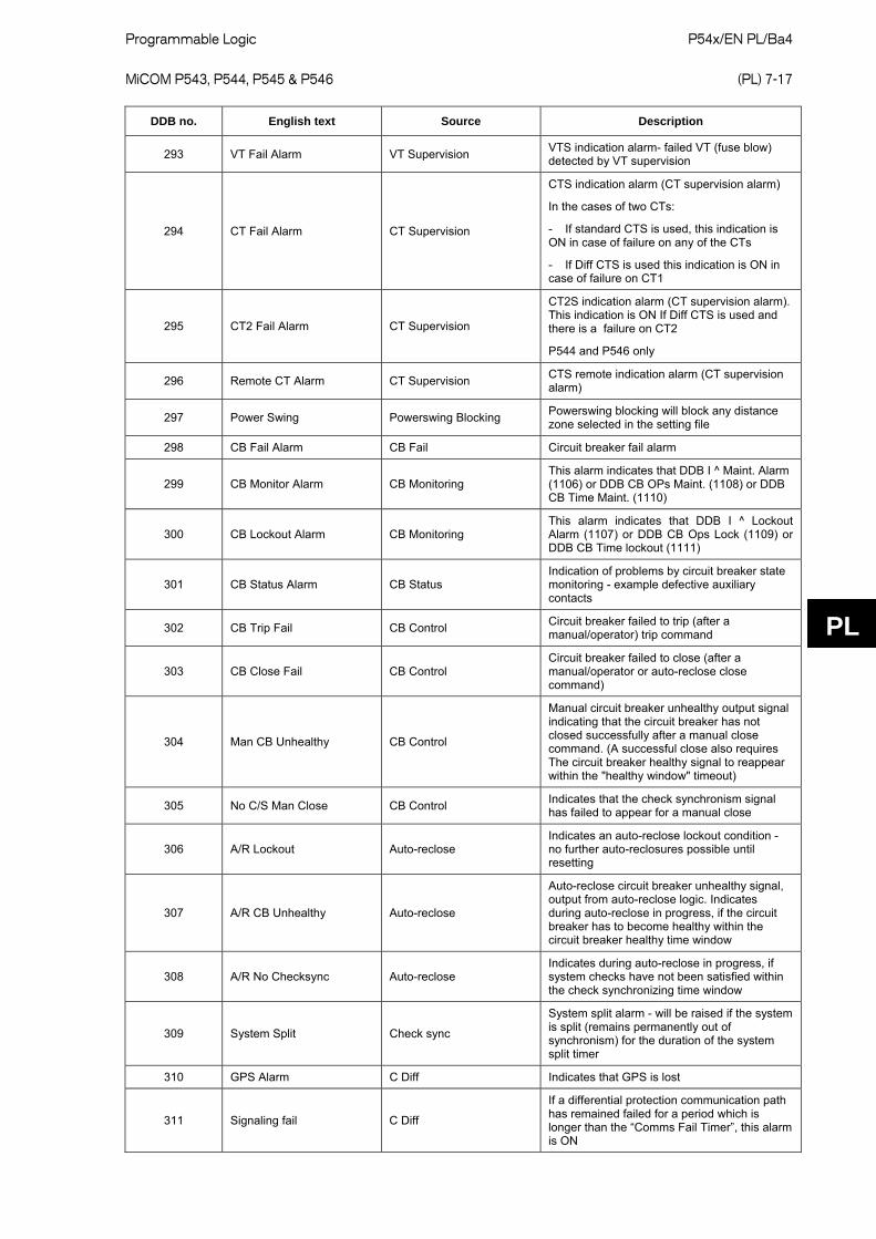
Programmable Logic P54x/EN PL/Ba4 MiCOM P543, P544, P545 & P546
(PL) 7-17
PL
DDB no. English text Source Description
293 VT Fail Alarm VT Supervision VTS indication alarm- failed VT (fuse blow) detected by VT supervision
294 CT Fail Alarm CT Supervision
CTS indication alarm (CT supervision alarm)
In the cases of two CTs:
- If standard CTS is used, this indication is ON in case of failure on any of the CTs
- If Diff CTS is used this indication is ON in case of failure on CT1
295 CT2 Fail Alarm CT Supervision
CT2S indication alarm (CT supervision alarm). This indication is ON If Diff CTS is used and there is a failure on CT2
P544 and P546 only
296 Remote CT Alarm CT Supervision CTS remote indication alarm (CT supervision alarm)
297 Power Swing Powerswing Blocking Powerswing blocking will block any distance zone selected in the setting file
298 CB Fail Alarm CB Fail Circuit breaker fail alarm
299 CB Monitor Alarm CB Monitoring This alarm indicates that DDB I ^ Maint. Alarm (1106) or DDB CB OPs Maint. (1108) or DDB CB Time Maint. (1110)
300 CB Lockout Alarm CB Monitoring This alarm indicates that DDB I ^ Lockout Alarm (1107) or DDB CB Ops Lock (1109) or DDB CB Time lockout (1111)
301 CB Status Alarm CB Status Indication of problems by circuit breaker state monitoring - example defective auxiliary contacts
302 CB Trip Fail CB Control Circuit breaker failed to trip (after a manual/operator) trip command
303 CB Close Fail CB Control Circuit breaker failed to close (after a manual/operator or auto-reclose close command)
304 Man CB Unhealthy CB Control
Manual circuit breaker unhealthy output signal indicating that the circuit breaker has not closed successfully after a manual close command. (A successful close also requires The circuit breaker healthy signal to reappear within the "healthy window" timeout)
305 No C/S Man Close CB Control Indicates that the check synchronism signal has failed to appear for a manual close
306 A/R Lockout Auto-reclose Indicates an auto-reclose lockout condition - no further auto-reclosures possible until resetting
307 A/R CB Unhealthy Auto-reclose
Auto-reclose circuit breaker unhealthy signal, output from auto-reclose logic. Indicates during auto-reclose in progress, if the circuit breaker has to become healthy within the circuit breaker healthy time window
308 A/R No Checksync Auto-reclose Indicates during auto-reclose in progress, if system checks have not been satisfied within the check synchronizing time window
309 System Split Check sync
System split alarm - will be raised if the system is split (remains permanently out of synchronism) for the duration of the system split timer
310 GPS Alarm C Diff Indicates that GPS is lost
311 Signaling fail C Diff
If a differential protection communication path has remained failed for a period which is longer than the “Comms Fail Timer”, this alarm is ON

P54x/EN PL/Ba4 Programmable Logic
(PL) 7-18
MiCOM P543, P544, P545 & P546
PL
DDB no. English text Source Description
312 Comm Delay Alarm C Diff If successive calculated propagation delay times exceed time delay setting “Comm Delay Tol”, this alarms is ON
313 C Diff Failure C Diff It indicates that differential protection communications are completely lost and therefore C diff does not work
314 IM64 SchemeFail It indicates that communications between relays are completely lost and therefore IM64 does not work
315 IEEE C37.94 Fail C Diff
It will appear in case of at least one of the following: CH1 (or CH2) loss of signal, CH1 (or CH2) PATH_YELLOW or CH1 (or CH2) BAD_RX_N
316 C Diff Inhibited C Diff Indicate that a differential protection has been inhibited
317 Aid 1 Chan Fail PSL Aided channel scheme 1 - channel out of service indication, indicating channel failure
318 Aid 2 Chan Fail PSL Aided channel scheme 2 - channel out of service indication, indicating channel failure
319 F out of Range Frequency Tracking Frequency out of range alarm
320 CB2 Fail Alarm CB2 Fail
Circuit breaker 2 fail alarm
P544 and P546 only
321 CB2 Monitor Alm CB2 Monitoring
This alarm indicates that DDB CB2 I ^ Maint. Alarm (1113) or DDB CB2 OPs Maint. (1115) or DDB CB2 Time Maint. (1117)
P544 and P546 only
322 CB2 Mon LO Alarm CB2 Monitoring
This alarm indicates that DDB CB2 I ^ Lockout Alarm (1114) or DDB CB Ops Lock (1116) or DDB CB Time lockout (1118)
P544 and P546 only
323 CB2 Status Alarm CB2 Status
Indication of problems by circuit breaker 2 state monitoring - example defective auxiliary contacts
P544 and P546 only
324 CB2 Trip Fail CB2 Control Circuit breaker 2 failed to trip (after a manual/operator) trip command
P544 and P546 only
325 CB2 Close Fail CB2 Control
Circuit breaker 2 failed to close (after a manual/operator or auto-reclose close command)
P544 and P546 only
326 Man CB2 Unhealthy CB2 Control
Manual circuit breaker unhealthy output signal indicating that the circuit breaker 2 has not closed successfully after a manual close command. (A successful close also requires The circuit breaker healthy signal to reappear within the "healthy window" timeout)
P544 and P546 only
327 NoCS CB2ManClose CB2 Control Indicates that the check synchronism signal has failed to appear for a manual close
P544 and P546 only
328 AR CB2 Lockout CB2 Auto-reclose
Indicates an auto-reclose lockout condition - no further auto-reclosures possible until resetting
P544 and P546 only

Programmable Logic P54x/EN PL/Ba4 MiCOM P543, P544, P545 & P546
(PL) 7-19
PL
DDB no. English text Source Description
329 AR CB2 Unhealthy CB2 Auto-reclose
Auto-reclose circuit breaker unhealthy signal, output from auto-reclose logic. Indicates during auto-reclose in progress, if the circuit breaker has to become healthy within the circuit breaker healthy time window
P544 and P546 only
330 AR CB2 No C/S CB2 Auto-reclose
Indicates during auto-reclose in progress, if system checks have not been satisfied within the check synchronizing time window
P544 and P546 only
331 Invalid AR Mode Auto-reclose AR Mode selected via optos is not supported
P544 and P546 only
332 to 333 Not used
334 Main Prot. Fail Co-processor Interface Indicates a failure in differential or distance or DEF
335 Config Error C Diff
In three ended schemes on power up, the relays check to see if one of them should be configured out. Under some circumstances it is possible for them to fail to resolve this in which case they produce the DDB_CONFIGURATION_ERROR alarm
336 Re-Config Error C Diff Indicates that RESTORE or RECONFIGURE or CONFIGURE operations have failed
335, 336 Not used
337 Comms Changed C Diff This is an alarm which indicates that C3794 comms have been changed to standard or vice versa and relay must be rebooted
338 to 343 Not used
344 SR User Alarm 1 PSL Triggers user alarm 1 message to be alarmed on LCD display (self-resetting)
347 SR User Alarm 4 PSL Triggers user alarm 4 message to be alarmed on LCD display (self-resetting)
348 MR User Alarm 5 PSL Triggers user alarm 5 message to be alarmed on LCD display (manual-resetting)
351 MR User Alarm 8 PSL Triggers user alarm 8 message to be alarmed on LCD display (manual-resetting)
352 Battery Fail Self Monitoring Front panel miniature battery failure - either battery removed from slot, or low voltage
353 Field Volts Fail Self Monitoring 48V field voltage failure
354 Rear Comm 2 Fail Self Monitoring Comm2 hardware failure - second rear communications board
355 GOOSE IED Absent The IED is not subscribed to a publishing IED in the current scheme
356 NIC Not Fitted Ethernet board not fitted
357 NIC No Response Ethernet board not responding
358 NIC Fatal Error Ethernet board unrecoverable error
359 NIC Soft. Reload Ethernet problem
360 Bad TCP/IP Cfg. Ethernet problem
361 Bad OSI Config. Ethernet problem
362 NIC Link Fail Ethernet link lost
363 NIC SW Mis-Match Ethernet board software not compatible with main CPU
364 IP Addr Conflict The IP address of the IED is already used by another IED
365 to 368 Not used

P54x/EN PL/Ba4 Programmable Logic
(PL) 7-20
MiCOM P543, P544, P545 & P546
PL
DDB no. English text Source Description
369 Backup setting Self Monitoring
This is an alarm that is ON if any setting fail during the setting changing process. If this happens, the relay will use the last known good setting
370 to 383 Not used
384 Block Zone 1 Gnd PSL Zone 1 ground basic scheme blocking
385 Block Zone 1 Phs PSL Zone 1 phase basic scheme blocking
386 Block Zone 2 Gnd PSL Zone 2 ground basic scheme blocking
387 Block Zone 2 Phs PSL Zone 2 phase basic scheme blocking
388 Block Zone 3 Gnd PSL Zone 3 ground basic scheme blocking
389 Block Zone 3 Phs PSL Zone 3 phase basic scheme blocking
390 Block Zone P Gnd PSL Zone P ground basic scheme blocking
391 Block Zone P Phs PSL Zone P phase basic scheme blocking
392 Block Zone 4 Gnd PSL Zone 4 ground basic scheme blocking
393 Block Zone 4 Phs PSL Zone 4 phase basic scheme blocking
394 Aid1 InhibitDist PSL Block distance aided scheme 1 tripping
395 Aid1 Inhibit DEF PSL Block DEF aided scheme 1 tripping
396 Aid1 Inhibit DIR PSL Block Delta directional aided scheme 1 tripping
397 Aid2 InhibitDist PSL Block distance aided scheme 2 tripping
398 Aid2 Inhibit DEF PSL Block DEF aided scheme 2 tripping
399 Aid2 Inhibit DIR PSL Block Delta directional aided scheme 2 tripping
400 Time Synch PSL Time synchronism by opto pulse
401 I>1 Timer Block PSL Block phase overcurrent stage 1 time delayed tripped trip
402 I>2 Timer Block PSL Block phase overcurrent stage 2 time delayed tripped trip
403 I>3 Timer Block PSL Block phase overcurrent stage 3 time delayed trip
404 I>4 Timer Block PSL Block phase overcurrent stage 4 time delayed trip
405 IN>1 Timer Block PSL Block standby earth fault stage 1 time delayed trip
406 IN>2 Timer Block PSL Block standby earth fault stage 2 time delayed trip
407 IN>3 Timer Block PSL Block standby earth fault stage 3 time delayed trip
408 IN>4 Timer Block PSL Block standby earth fault stage 4 time delayed trip
409 ISEF>1 Timer Blk PSL Block sensitive earth fault stage 1 time delayed trip
410 ISEF>2 Timer Blk PSL Block sensitive earth fault stage 2 time delayed trip
411 ISEF>3 Timer Blk PSL Block sensitive earth fault stage 3 time delayed trip
412 ISEF>4 Timer Blk PSL Block sensitive earth fault stage 4 time delayed trip
413 Not used
414 V<1 Timer Block PSL Block phase undervoltage stage 1 time delayed trip
415 V<2 Timer Block PSL Block phase undervoltage stage 2 time delayed trip
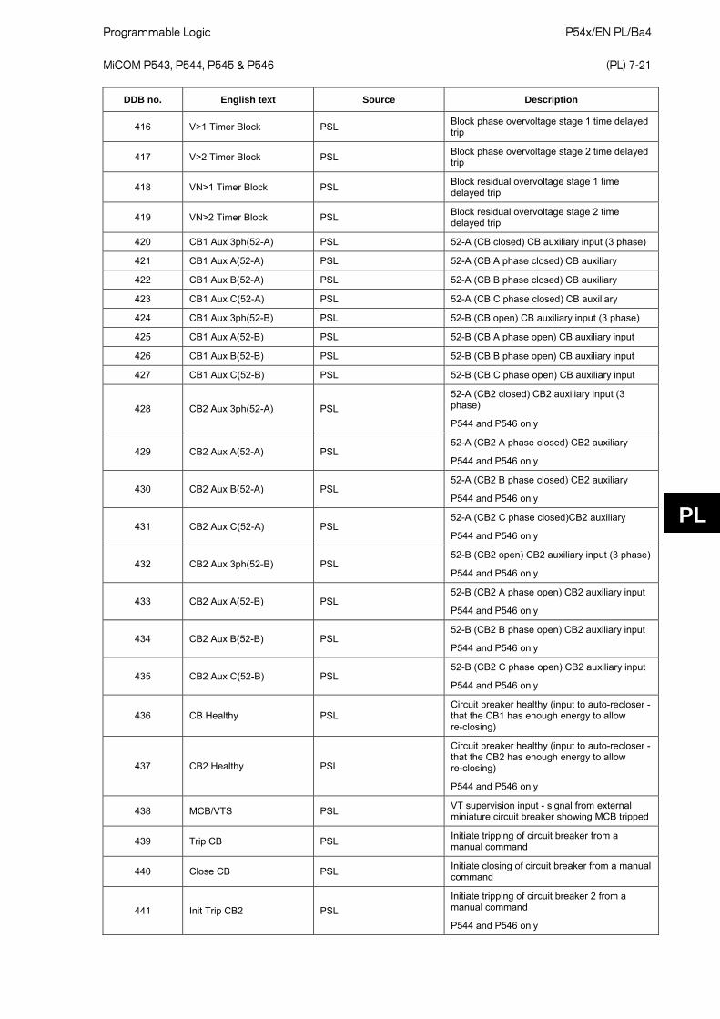
Programmable Logic P54x/EN PL/Ba4 MiCOM P543, P544, P545 & P546
(PL) 7-21
PL
DDB no. English text Source Description
416 V>1 Timer Block PSL Block phase overvoltage stage 1 time delayed trip
417 V>2 Timer Block PSL Block phase overvoltage stage 2 time delayed trip
418 VN>1 Timer Block PSL Block residual overvoltage stage 1 time delayed trip
419 VN>2 Timer Block PSL Block residual overvoltage stage 2 time delayed trip
420 CB1 Aux 3ph(52-A) PSL 52-A (CB closed) CB auxiliary input (3 phase)
421 CB1 Aux A(52-A) PSL 52-A (CB A phase closed) CB auxiliary
422 CB1 Aux B(52-A) PSL 52-A (CB B phase closed) CB auxiliary
423 CB1 Aux C(52-A) PSL 52-A (CB C phase closed) CB auxiliary
424 CB1 Aux 3ph(52-B) PSL 52-B (CB open) CB auxiliary input (3 phase)
425 CB1 Aux A(52-B) PSL 52-B (CB A phase open) CB auxiliary input
426 CB1 Aux B(52-B) PSL 52-B (CB B phase open) CB auxiliary input
427 CB1 Aux C(52-B) PSL 52-B (CB C phase open) CB auxiliary input
428 CB2 Aux 3ph(52-A) PSL 52-A (CB2 closed) CB2 auxiliary input (3 phase)
P544 and P546 only
429 CB2 Aux A(52-A) PSL 52-A (CB2 A phase closed) CB2 auxiliary
P544 and P546 only
430 CB2 Aux B(52-A) PSL 52-A (CB2 B phase closed) CB2 auxiliary
P544 and P546 only
431 CB2 Aux C(52-A) PSL 52-A (CB2 C phase closed)CB2 auxiliary
P544 and P546 only
432 CB2 Aux 3ph(52-B) PSL 52-B (CB2 open) CB2 auxiliary input (3 phase)
P544 and P546 only
433 CB2 Aux A(52-B) PSL 52-B (CB2 A phase open) CB2 auxiliary input
P544 and P546 only
434 CB2 Aux B(52-B) PSL 52-B (CB2 B phase open) CB2 auxiliary input
P544 and P546 only
435 CB2 Aux C(52-B) PSL 52-B (CB2 C phase open) CB2 auxiliary input
P544 and P546 only
436 CB Healthy PSL Circuit breaker healthy (input to auto-recloser - that the CB1 has enough energy to allow re-closing)
437 CB2 Healthy PSL
Circuit breaker healthy (input to auto-recloser - that the CB2 has enough energy to allow re-closing)
P544 and P546 only
438 MCB/VTS PSL VT supervision input - signal from external miniature circuit breaker showing MCB tripped
439 Trip CB PSL Initiate tripping of circuit breaker from a manual command
440 Close CB PSL Initiate closing of circuit breaker from a manual command
441 Init Trip CB2 PSL Initiate tripping of circuit breaker 2 from a manual command
P544 and P546 only

P54x/EN PL/Ba4 Programmable Logic
(PL) 7-22
MiCOM P543, P544, P545 & P546
PL
DDB no. English text Source Description
442 Init Close CB2 PSL Initiate closing of circuit breaker 2 from a manual command
P544 and P546 only
443 Reset Close Dly PSL Reset manual circuit breaker close time delay
444 Reset Relays/LED PSL Reset latched relays & LEDs (manual reset of any lockout trip contacts, auto-reclose lockout, and LEDs)
445 Reset Thermal PSL Reset thermal state to 0%
446 Reset (CB1) Lockout PSL Manual control to reset auto-recloser from lockout
447 Reset CB (1) Data PSL Reset circuit breaker maintenance values
448 BAR (P543 and P545)
Block CB1 AR (P544 and P546)
PSL Block the Auto-reclose function (CB1 only in P544 and P546) from an external input
449 En 1pole reclose PSL Enable 1 pole reclose from an external input
P543/P545 only
450 En 3pole reclose PSL Enable 3 pole reclose from an external input
P543/P545 only
451 Pole Discrepancy (CB1) PSL Pole discrepancy (from external detector) - input used to force a 2nd single pole trip to move to a 3 pole auto-reclose cycle
452 Loopback Mode PSL To enable loopback mode via opto input
453 Perm Intertrip Permissive intertrip mapping what will be sent to the remote line end
454 Stub Bus Enabled
To enable stub bus protection in relays with two CT inputs. When enabled, all current values transmitted to the remote relays, and all those received from remote relays, are set to zero. Differential intertrip signals are not sent The protection provides differential protection for the stub zone
455 Inhibit C Diff When linked to an opto input, inhibits differential relay at the local end and send an inhibit command to the remote end
456 Recon Interlock
This must be energized (along with DDB 455 - inhibit C Diff) at the time that a relay configuration is changed from 3 ended to 2 ended scheme. This usually should be driven from a 52-B contact of the CB connected to the line end that is taken out of service
457 Prop Delay Equal PSL
If a P54x relay working with GPS sample synchronization loses GPS and there is a further switch in the protection communications network, the relay becomes Inhibit. If GPS become active again, the relay will automatically reset. But if not, the user can remove the inhibited condition by energizing this DDB signal as long as it is ensured that propagation delay times are equal
458 Inhibit WI PSL Inhibit weak infeed aided scheme logic
459 Test Mode PSL Commissioning tests - automatically places relay in test mode
460 Command Blocking PSL For IEC-870-5-103 protocol only, used for "Command Blocking" (relay ignores SCADA commands)
461 Monitor Blocking PSL For IEC-870-5-103 protocol only, used for "Monitor Blocking" (relay is quiet - issues no messages via SCADA port)
462 Not used

Programmable Logic P54x/EN PL/Ba4 MiCOM P543, P544, P545 & P546
(PL) 7-23
PL
DDB no. English text Source Description
463 Inhibit I>1 PSL Inhibit stage 1 overcurrent protection
464 Inhibit I>2 PSL Inhibit stage 2 overcurrent protection
465 Inhibit I>3 PSL Inhibit stage 3 overcurrent protection
466 Inhibit I>4 PSL Inhibit stage 4 overcurrent protection
467 Inhibit IN>1 PSL Inhibit stage 1 earth fault protection
468 Inhibit IN>2 PSL Inhibit stage 2 earth fault protection
469 Inhibit IN>3 PSL Inhibit stage 3 earth fault protection
470 Inhibit IN>4 PSL Inhibit stage 4 earth fault protection
471 Inhibit V<1 PSL Inhibit stage 1 undervoltage protection
472 Inhibit V<2 PSL Inhibit stage 2 undervoltage protection
473 Inhibit V>1 PSL Inhibit stage 1 overvoltage protection
474 Inhibit V>2 PSL Inhibit stage 2 overvoltage protection
475 Inhibit VN>1 PSL Inhibit stage 1 residual overvoltage protection
476 Inhibit VN>2 PSL Inhibit stage 2 residual overvoltage protection
477 Not used
478 Inhibit Thermal PSL Inhibit thermal overload protection
479 Inhibit CB Status PSL Inhibit circuit breaker state monitoring (no alarm for defective/stuck auxiliary contact)
480 Inhibit CB Fail PSL Inhibit circuit breaker fail protection
481 Inhibit OpenLine PSL Broken conductor protection
482 Inhibit VTS PSL Inhibit VT supervision (including turn OF MCB’s) via PSL
483 Inhibit CTS PSL Inhibit CT supervision (both differential and standard CTS) via PSL
484 InhibitChecksync PSL Inhibit checksync
485 Inhibit TOR PSL Inhibit trip on reclose (TOR)
486 Inhibit SOTF PSL Inhibit switch onto fault (SOTF)
487 Disable Diff CTS PSL To disable differential CTS via PSL
488 Set SOTF PSL
To enable SOTF logic by an external pulse. When this input is energized by en external pulse, SOTF becomes enabled during “SOTF Pulse” time setting
489 AR Reset Z1 EXT Zone 1 Extension Scheme AR reset Z1X reach back to Z1 reach in Z1 extension scheme
490 Reset Zone 1 Ext PSL Reset zone Z1X back to Z1 reach using logic input (i.e. case when external AR and Z1 extension scheme are used)
491 Inhibit LoL PSL Inhibit Loss of Load scheme function
492 Aided 1 COS/LGS PSL
Aided 1 channel out of service signal (COS) or loss of guard signal (LGS) in distance unblocking schemes. This signal is normally driven from an opto input on conventional channels or from InterMiCOM
493 Aided1 Scheme Rx PSL Aided channel 1 - external signal received, for input to distance fixed scheme logic
494 Aided 1 Receive Aided Scheme Logic Aided channel 1 - internal signal received generated in the signal receive logic
495 Not used
496 Aid1 Block Send PSL Prevent sending by customized logic - aided scheme 1
497 Aid1 Custom Send PSL Programmable send logic for special customized scheme (aided channel 1)

P54x/EN PL/Ba4 Programmable Logic
(PL) 7-24
MiCOM P543, P544, P545 & P546
PL
DDB no. English text Source Description
498 Aided 1 Send Aided Scheme Logic Aided channel 1 send - internal send signal generated in signal send logic
499 Aid1 Custom T In PSL
When using a custom programmable aided scheme 1, the user is able to include a current reversal guard timer. Energizing this DDB will additionally start this timer, from PSL
500 Aid1 CustomT Out Aided Scheme Logic
When using customized aided scheme 1, this signal is used to indicate any additional condition that should be treated as permission for an aided trip (for example a permissive signal received could be connected, or a blocking signal could be inverted and then connected)
501 Aid1 Trip Enable Aided Scheme Logic
Aided scheme 1 trip enable - this is a permissive signal used to accelerate zone 2, or a blocking signal which has been inverted. It is a signal output, part-way through the internal fixed logic of aided schemes
502 Aid1 Custom Trip PSL Aid1 custom trip enable
503 Aid 1 Dist Trip Aided Scheme Logic Aided scheme 1 distance trip command (output from aided tripping logic)
504 Aid 1 Delta Trip Aided Scheme Logic Aided Scheme 1 Delta Directional Trip command (output from Aided tripping logic)
505 Aid 1 DEF Trip Aided Scheme Logic Aided scheme 1 DEF trip command (output from aided tripping logic)
506 Aided 2 COS/LGS PSL
Aided 2 channel out of service signal (COS) or loss of guard signal (LGS) in distance unblocking schemes. This signal is normally driven from an opto input on conventional channels or from InterMiCOM
507 Aided2 Scheme Rx PSL Aided channel 2 - external signal received, for input to distance fixed scheme logic
508 Aided 2 Receive Aided Scheme Logic Aided channel 2 - internal signal received generated in the signal receive logic
509 to 511 Not used
512 Aid2 Block Send PSL Prevent sending by customized logic - aided scheme 2
513 Aid2 Custom Send PSL Programmable send logic for special customized scheme (aided channel 2)
514 Aided 2 Send Aided Scheme Logic Aided channel 2 send - internal send signal generated in signal send logic
515 Aid2 Custom T In PSL
When using a custom programmable aided scheme 2, the user is able to include a current reversal guard timer. Energizing this DDB will additionally start this timer, from PSL
516 Aid2 CustomT Out Aided Scheme Logic
When using customized aided scheme 2, this signal is used to indicate any additional condition that should be treated as permission for an aided trip (for example a permissive signal received could be connected, or a blocking signal could be inverted and then connected)
517 Aid2 Trip Enable Aided Scheme Logic
Aided scheme 2 trip enable - this is a permissive signal used to accelerate zone 2, or a blocking signal which has been inverted. It is a signal output, part-way through the internal fixed logic of aided schemes
518 Aid2 Custom Trip PSL Aid2 custom trip enable
519 Aid 2 Dist Trip Aided Scheme Logic Aided scheme 2 distance trip command (output from aided tripping logic)
520 Aid 2 Delta Trip Aided Scheme Logic Aided Scheme 2 Delta Directional Trip command (output from Aided tripping logic)

Programmable Logic P54x/EN PL/Ba4 MiCOM P543, P544, P545 & P546
(PL) 7-25
PL
DDB no. English text Source Description
521 Aid 2 DEF Trip Aided Scheme Logic Aided scheme 2 DEF trip command (output from aided tripping logic)
522 Any Trip Trip Conversion Logic Any trip signal - can be used as the trip command in three-pole tripping applications
523 Trip Output A (CB1) Trip Conversion Logic Trip signal for phase A - used as a command to drive trip A output contact(s). Takes the output from the internal trip conversion logic
524 Trip Output B (CB1) Trip Conversion Logic Trip signal for phase B - used as a command to drive trip B output contact(s). Takes the output from the internal trip conversion logic
525 Trip Output C (CB1) Trip Conversion Logic Trip signal for phase C - used as a command to drive trip C output contact(s). Takes the output from the internal trip conversion logic
526 Trip 3ph (CB1) Trip Conversion Logic 3 phase trip command
527 2/3 Ph Fault Trip Conversion Logic
2 or 3 phase fault indication - used to flag whether the fault is polyphase. Typically used to control auto-reclose logic, where auto-reclosing is allowed only for single phase faults
528 3 Ph Fault Trip Conversion Logic
3 phase fault indication. Typically used to control auto-reclose logic, where auto-reclosing is blocked for faults affecting all three phases together
529 Trip Inputs 3Ph (CB1) PSL Trip 3 phase - input to trip latching logic
530 Trip Inputs A PSL
A phase trip - input to trip conversion logic. Essential to ensure correct single or three pole trip command results (e.g. converts a 2 pole trip to 3 phase)
531 Trip Inputs B PSL
B phase trip - input to trip conversion logic. Essential to ensure correct single or three pole trip command results (e.g. converts a 2 pole trip to 3 phase)
532 Trip Inputs C PSL
C phase trip - input to trip conversion logic. Essential to ensure correct single or three pole trip command results (e.g. converts a 2 pole trip to 3 phase)
533 Force 3Pole Trip (CB1) PSL
Force any trip which is issued to always be 3 pole (trip conversion - used in single pole trip applications, to signal when single pole tripping and re-closing is either unwanted, or impossible)
534 External Trip3ph (or CB1 Ext Trip3Ph) PSL
External trip 3 phase - allows external protection to initiate breaker fail, circuit breaker condition monitoring statistics, and internal auto-reclose (if enabled)
535 External Trip A (or CB1 Ext Trip A) PSL
External trip A phase - allows external protection to initiate breaker fail, circuit breaker condition monitoring statistics, and internal auto-reclose (if enabled)
536 External Trip B (or CB1 Ext Trip B) PSL
External trip B phase - allows external protection to initiate breaker fail, circuit breaker condition monitoring statistics, and internal auto-reclose (if enabled)
537 External Trip C (or CB1 Ext Trip C) PSL
External trip C phase - allows external protection to initiate breaker fail, circuit breaker condition monitoring statistics, and internal auto-reclose (if enabled)
538 CB2 Ext Trip3ph PSL External trip 3 phase - allows external protection to initiate breaker 2 fail
P544 and P546 only
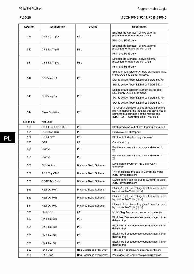
P54x/EN PL/Ba4 Programmable Logic
(PL) 7-26
MiCOM P543, P544, P545 & P546
PL
DDB no. English text Source Description
539 CB2 Ext Trip A PSL External trip A phase - allows external protection to initiate breaker 2 fail
P544 and P546 only
540 CB2 Ext Trip B PSL External trip B phase - allows external protection to initiate breaker 2 fail
P544 and P546 only
541 CB2 Ext Trip C PSL External trip C phase - allows external protection to initiate breaker 2 fail
P544 and P546 only
542 SG Select x1 PSL
Setting group selector X1 (low bit)-selects SG2 if only DDB 542 signal is active.
SG1 is active if both DDB 542 & DDB 543=0
SG4 is active if both DDB 542 & DDB 543=1
543 SG Select 1x PSL
Setting group selector 1X (high bit)-selects SG3 if only DDB 543 is active.
SG1 is active if both DDB 542 & DDB 543=0
SG4 is active if both DDB 542 & DDB 543=1
544 Clear Statistics PSL
To reset all statistics values cumulated on the relay. If mapped, the input for this signal could come from a command of the remote end (DDB 1020 - clear stats cmd -) via IM64
545 to 549 Not used
550 Inhibit Predictive OST PSL Block predictive out of step tripping command
551 Predictive OST PSL Predictive out of step trip
552 Inhibit OST PSL Block out of step tripping command
553 OST PSL Out of step trip
554 Start Z5 PSL Positive sequence impedance is detected in Z5
555 Start Z6 PSL Positive sequence impedance is detected in Z6
556 CNV Active Distance Basic Scheme Level detector Current No Volts (CNV) exceeded
557 TOR Trip CNV Distance Basic Scheme Trip on Reclose trip due to Current No Volts (CNV) level detectors
558 SOTF Trip CNV Distance Basic Scheme Switch on to Fault trip due to Current No Volts (CNV) level detectors
559 Fast OV PHA Distance Basic Scheme Phase A Fast Overvoltage level detector used by Current No Volts (CNV)
560 Fast OV PHB Distance Basic Scheme Phase B Fast Overvoltage level detector used by Current No Volts (CNV)
561 Fast OV PHC Distance Basic Scheme Phase C Fast Overvoltage level detector used by Current No Volts (CNV)
562 I2> Inhibit PSL Inhibit Neg Sequence overcurrent protection
563 I2>1 Tmr Blk PSL Block Neg Sequence overcurrent stage 1 time delayed trip
564 I2>2 Tmr Blk PSL Block Neg Sequence overcurrent stage 2 time delayed trip
565 I2>3 Tmr Blk PSL Block Neg Sequence overcurrent stage 3 time delayed trip
566 I2>4 Tmr Blk PSL Block Neg Sequence overcurrent stage 4 time delayed trip
567 I2>1 Start Neg Sequence overcurrent 1st stage Neg Sequence overcurrent start
568 I2>2 Start Neg Sequence overcurrent 2nd stage Neg Sequence overcurrent start

Programmable Logic P54x/EN PL/Ba4 MiCOM P543, P544, P545 & P546
(PL) 7-27
PL
DDB no. English text Source Description
569 I2>3 Start Neg Sequence overcurrent 3rd stage Neg Sequence overcurrent start
570 I2>4 Start Neg Sequence overcurrent 4th stage Neg Sequence overcurrent start
571 I2>1 Trip Neg Sequence overcurrent 1st stage Neg Sequence overcurrent trip
572 I2>2 Trip Neg Sequence overcurrent 2nd stage Neg Sequence overcurrent trip
573 I2>3 Trip Neg Sequence overcurrent 3rd stage Neg Sequence overcurrent trip
574 I2>4 Trip Neg Sequence overcurrent 4th stage Neg Sequence overcurrent trip
575 Not used
576 AR Trip Test Commissioning Test
Auto-reclose trip test cycle in progress. Indication that a manually-initiated test cycle is in progress
P543 and P545 only
577 AR Trip Test A Commissioning Test Auto-reclose trip test A phase. Indication that a manually-initiated test cycle is in progress
578 AR Trip Test B Commissioning Test Auto-reclose trip test B phase. Indication that a manually-initiated test cycle is in progress
579 AR Trip Test C Commissioning Test Auto-reclose trip test C phase. Indication that a manually-initiated test cycle is in progress
580 AR Init 3Ph Auto-Reclose Initiate 3 phase auto-reclose (signal to an external re-closer)
P543 and P545 only
581 Not used
582 Diff Trip C Diff Current differential trip
583 Diff Trip A C Diff Current differential A phase trip
584 Diff Trip B C Diff Current differential B phase trip
585 Diff Trip C C Diff Current differential C phase trip
586 Diff InterTrip C Diff Current differential intertrip
587 Diff InterTrip A C Diff Current differential A phase intertrip
588 Diff InterTrip B C Diff Current differential B phase intertrip
589 Diff InterTrip C C Diff Current differential C phase intertrip
590 Perm InterTrip C Diff Permissive intertrip
591 Stub Bus Trip C Diff Stub bus trip
592 df/dt> Inhibit PSL Inhibit df/dt protection
593 df/dt>1 Tmr Blk PSL Block df/dt Stage 1 Timer
594 df/dt>2 Tmr Blk PSL Block df/dt Stage 2 Timer
595 df/dt>3 Tmr Blk PSL Block df/dt Stage 3 Timer
596 df/dt>4 Tmr Blk PSL Block df/dt Stage 4 Timer
597 df/dt>1 Start df/dt protection df/dt Stage 1 Start
598 df/dt>2 Start df/dt protection df/dt Stage 2 Start
599 df/dt>3 Start df/dt protection df/dt Stage 3 Start
600 df/dt>4 Start df/dt protection df/dt Stage 4 Start
601 df/dt>1 Trip df/dt protection df/dt Stage 1 Trip
602 df/dt>2 Trip df/dt protection df/dt Stage 2 Trip
603 df/dt>3 Trip df/dt protection df/dt Stage 3 Trip
604 df/dt>4 Trip df/dt protection df/dt Stage 4 Trip
605 Not used
608 Zone 1 Trip Distance Basic Scheme Zone 1 trip
609 Zone 1 A Trip Distance Basic Scheme Zone 1 A phase trip
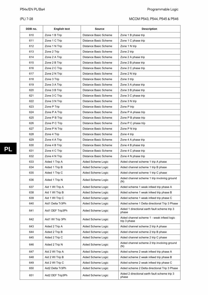
P54x/EN PL/Ba4 Programmable Logic
(PL) 7-28
MiCOM P543, P544, P545 & P546
PL
DDB no. English text Source Description
610 Zone 1 B Trip Distance Basic Scheme Zone 1 B phase trip
611 Zone 1 C Trip Distance Basic Scheme Zone 1 C phase trip
612 Zone 1 N Trip Distance Basic Scheme Zone 1 N trip
613 Zone 2 Trip Distance Basic Scheme Zone 2 trip
614 Zone 2 A Trip Distance Basic Scheme Zone 2 A phase trip
615 Zone 2 B Trip Distance Basic Scheme Zone 2 B phase trip
616 Zone 2 C Trip Distance Basic Scheme Zone 2 C phase trip
617 Zone 2 N Trip Distance Basic Scheme Zone 2 N trip
618 Zone 3 Trip Distance Basic Scheme Zone 3 trip
619 Zone 3 A Trip Distance Basic Scheme Zone 3 A phase trip
620 Zone 3 B Trip Distance Basic Scheme Zone 3 B phase trip
621 Zone 3 C Trip Distance Basic Scheme Zone 3 C phase trip
622 Zone 3 N Trip Distance Basic Scheme Zone 3 N trip
623 Zone P Trip Distance Basic Scheme Zone P trip
624 Zone P A Trip Distance Basic Scheme Zone P A phase trip
625 Zone P B Trip Distance Basic Scheme Zone P B phase trip
626 Zone P C Trip Distance Basic Scheme Zone P C phase trip
627 Zone P N Trip Distance Basic Scheme Zone P N trip
628 Zone 4 Trip Distance Basic Scheme Zone 4 trip
629 Zone 4 A Trip Distance Basic Scheme Zone 4 A phase trip
630 Zone 4 B Trip Distance Basic Scheme Zone 4 B phase trip
631 Zone 4 C Trip Distance Basic Scheme Zone 4 C phase trip
632 Zone 4 N Trip Distance Basic Scheme Zone 4 N phase trip
633 Aided 1 Trip A Aided Scheme Logic Aided channel scheme 1 trip A phase
634 Aided 1 Trip B Aided Scheme Logic Aided channel scheme 1 trip B phase
635 Aided 1 Trip C Aided Scheme Logic Aided channel scheme 1 trip C phase
636 Aided 1 Trip N Aided Scheme Logic Aided channel scheme 1 trip involving ground (N)
637 Aid 1 WI Trip A Aided Scheme Logic Aided scheme 1 weak infeed trip phase A
638 Aid 1 WI Trip B Aided Scheme Logic Aided scheme 1 weak infeed trip phase B
639 Aid 1 WI Trip C Aided Scheme Logic Aided scheme 1 weak infeed trip phase C
640 Aid1 Delta Tr3Ph Aided Scheme Logic Aided scheme 1 Delta directional Trip 3 Phase
641 Aid1 DEF Trip3Ph Aided Scheme Logic Aided 1 directional earth fault scheme trip 3 phase
642 Aid1 WI Trip 3Ph Aided Scheme Logic Aided channel scheme 1 - weak infeed logic trip 3 phase
643 Aided 2 Trip A Aided Scheme Logic Aided channel scheme 2 trip A phase
644 Aided 2 Trip B Aided Scheme Logic Aided channel scheme 2 trip B phase
645 Aided 2 Trip C Aided Scheme Logic Aided channel scheme 2 trip C phase
646 Aided 2 Trip N Aided Scheme Logic Aided channel scheme 2 trip involving ground (N)
647 Aid 2 WI Trip A Aided Scheme Logic Aided scheme 2 weak infeed trip phase A
648 Aid 2 WI Trip B Aided Scheme Logic Aided scheme 2 weak infeed trip phase B
649 Aid 2 WI Trip C Aided Scheme Logic Aided scheme 2 weak infeed trip phase C
650 Aid2 Delta Tr3Ph Aided Scheme Logic Aided scheme 2 Delta directional Trip 3 Phase
651 Aid2 DEF Trip3Ph Aided Scheme Logic Aided 2 directional earth fault scheme trip 3 phase

Programmable Logic P54x/EN PL/Ba4 MiCOM P543, P544, P545 & P546
(PL) 7-29
PL
DDB no. English text Source Description
652 Aid2 WI Trip 3Ph Aided Scheme Logic Aided channel scheme 2 - weak infeed logic trip 3 phase
653 Not used
654 Loss of Load Trip Loss of Load Logic Loss of load trip
655 I>1 Trip Overcurrent 1st stage phase overcurrent trip 3 phase
656 I>1 Trip A Overcurrent 1st stage phase overcurrent trip phase A
657 I>1 Trip B Overcurrent 1st stage phase overcurrent trip phase B
658 I>1 Trip C Overcurrent 1st stage phase overcurrent trip phase C
659 I>2 Trip Overcurrent 2nd stage phase overcurrent trip 3 phase
660 I>2 Trip A Overcurrent 2nd stage phase overcurrent trip phase A
661 I>2 Trip B Overcurrent 2nd stage phase overcurrent trip phase B
662 I>2 Trip C Overcurrent 2nd stage phase overcurrent trip phase C
663 I>3 Trip Overcurrent 3rd stage phase overcurrent trip 3 phase
664 I>3 Trip A Overcurrent 3rd stage phase overcurrent trip phase A
665 I>3 Trip B Overcurrent 3rd stage phase overcurrent trip phase B
666 I>3 Trip C Overcurrent 3rd stage phase overcurrent trip phase C
667 I>4 Trip Overcurrent 4th stage phase overcurrent trip 3 phase
668 I>4 Trip A Overcurrent 4th stage phase overcurrent trip phase A
669 I>4 Trip B Overcurrent 4th stage phase overcurrent trip phase B
670 I>4 Trip C Overcurrent 4th stage phase overcurrent trip phase C
671 IN>1 Trip Earth Fault 1st stage stand by earth fault (SBEF) protection trip
672 IN>2 Trip Earth Fault 2nd stage stand by earth fault (SBEF) protection trip
673 IN>3 Trip Earth Fault 3rd stage stand by earth fault (SBEF) protection trip
674 IN>4 Trip Earth Fault 4th stage stand by earth fault (SBEF) protection trip
675 ISEF>1 Trip Sensitive Earth Fault 1st stage sensitive earth fault (SEF) protection trip
676 ISEF>2 Trip Sensitive Earth Fault 2nd stage sensitive earth fault (SEF) protection trip
677 ISEF>3 Trip Sensitive Earth Fault 3rd stage sensitive earth fault (SEF) protection trip
678 ISEF>4 Trip Sensitive Earth Fault 4th stage sensitive earth fault (SEF) protection trip
679 Broken Wire Trip Broken Conductor Broken conductor trip
680 Thermal Trip Thermal Overload Thermal overload trip
683 V<1 Trip Undervoltage Undervoltage stage 1, three phase trip
684 V<1 Trip A/AB Undervoltage Undervoltage stage 1 A/AB phase trip
685 V<1 Trip B/BC Undervoltage Undervoltage stage 1 B/BC phase trip
686 V<1 Trip C/CA Undervoltage Undervoltage stage 1 C/CA phase trip
687 V<2 Trip Undervoltage Undervoltage stage 2, three phase trip
688 V<2 Trip A/AB Undervoltage Undervoltage stage 2 A/AB phase trip
689 V<2 Trip B/BC Undervoltage Undervoltage stage 2 B/BC phase trip
690 V<2 Trip C/CA Undervoltage Undervoltage stage 2 C/CA phase trip
691 V>1 Trip Overvoltage Overvoltage stage 1, three phase trip
692 V>1 Trip A/AB Overvoltage Overvoltage stage 1 A/AB phase trip
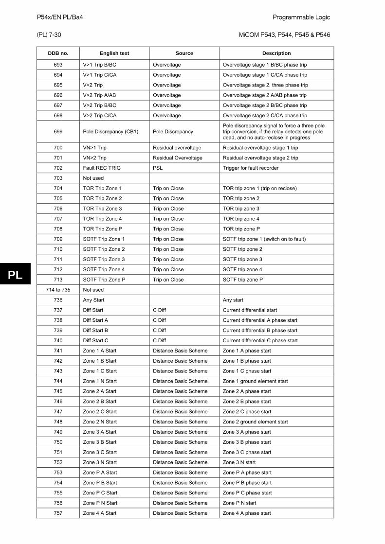
P54x/EN PL/Ba4 Programmable Logic
(PL) 7-30
MiCOM P543, P544, P545 & P546
PL
DDB no. English text Source Description
693 V>1 Trip B/BC Overvoltage Overvoltage stage 1 B/BC phase trip
694 V>1 Trip C/CA Overvoltage Overvoltage stage 1 C/CA phase trip
695 V>2 Trip Overvoltage Overvoltage stage 2, three phase trip
696 V>2 Trip A/AB Overvoltage Overvoltage stage 2 A/AB phase trip
697 V>2 Trip B/BC Overvoltage Overvoltage stage 2 B/BC phase trip
698 V>2 Trip C/CA Overvoltage Overvoltage stage 2 C/CA phase trip
699 Pole Discrepancy (CB1) Pole Discrepancy Pole discrepancy signal to force a three pole trip conversion, if the relay detects one pole dead, and no auto-reclose in progress
700 VN>1 Trip Residual overvoltage Residual overvoltage stage 1 trip
701 VN>2 Trip Residual Overvoltage Residual overvoltage stage 2 trip
702 Fault REC TRIG PSL Trigger for fault recorder
703 Not used
704 TOR Trip Zone 1 Trip on Close TOR trip zone 1 (trip on reclose)
705 TOR Trip Zone 2 Trip on Close TOR trip zone 2
706 TOR Trip Zone 3 Trip on Close TOR trip zone 3
707 TOR Trip Zone 4 Trip on Close TOR trip zone 4
708 TOR Trip Zone P Trip on Close TOR trip zone P
709 SOTF Trip Zone 1 Trip on Close SOTF trip zone 1 (switch on to fault)
710 SOTF Trip Zone 2 Trip on Close SOTF trip zone 2
711 SOTF Trip Zone 3 Trip on Close SOTF trip zone 3
712 SOTF Trip Zone 4 Trip on Close SOTF trip zone 4
713 SOTF Trip Zone P Trip on Close SOTF trip zone P
714 to 735 Not used
736 Any Start Any start
737 Diff Start C Diff Current differential start
738 Diff Start A C Diff Current differential A phase start
739 Diff Start B C Diff Current differential B phase start
740 Diff Start C C Diff Current differential C phase start
741 Zone 1 A Start Distance Basic Scheme Zone 1 A phase start
742 Zone 1 B Start Distance Basic Scheme Zone 1 B phase start
743 Zone 1 C Start Distance Basic Scheme Zone 1 C phase start
744 Zone 1 N Start Distance Basic Scheme Zone 1 ground element start
745 Zone 2 A Start Distance Basic Scheme Zone 2 A phase start
746 Zone 2 B Start Distance Basic Scheme Zone 2 B phase start
747 Zone 2 C Start Distance Basic Scheme Zone 2 C phase start
748 Zone 2 N Start Distance Basic Scheme Zone 2 ground element start
749 Zone 3 A Start Distance Basic Scheme Zone 3 A phase start
750 Zone 3 B Start Distance Basic Scheme Zone 3 B phase start
751 Zone 3 C Start Distance Basic Scheme Zone 3 C phase start
752 Zone 3 N Start Distance Basic Scheme Zone 3 N start
753 Zone P A Start Distance Basic Scheme Zone P A phase start
754 Zone P B Start Distance Basic Scheme Zone P B phase start
755 Zone P C Start Distance Basic Scheme Zone P C phase start
756 Zone P N Start Distance Basic Scheme Zone P N start
757 Zone 4 A Start Distance Basic Scheme Zone 4 A phase start

Programmable Logic P54x/EN PL/Ba4 MiCOM P543, P544, P545 & P546
(PL) 7-31
PL
DDB no. English text Source Description
758 Zone 4 B Start Distance Basic Scheme Zone 4 B phase start
759 Zone 4 C Start Distance Basic Scheme Zone 4 C phase start
760 Zone 4 N Start Distance Basic Scheme Zone 4 N start
761 I>1 Start Overcurrent 1st stage overcurrent start 3 phase
762 I>1 Start A Overcurrent 1st stage overcurrent start phase A
763 I>1 Start B Overcurrent 1st stage overcurrent start phase B
764 I>1 Start C Overcurrent 1st stage overcurrent start phase C
765 I>2 Start Overcurrent 2nd stage overcurrent start 3 phase
766 I>2 Start A Overcurrent 2nd stage overcurrent start phase A
767 I>2 Start B Overcurrent 2nd stage overcurrent start phase B
768 I>2 Start C Overcurrent 2nd stage overcurrent start phase C
769 I>3 Start Overcurrent 3rd stage overcurrent start 3 phase
770 I>3 Start A Overcurrent 3rd stage overcurrent start phase A
771 I>3 Start B Overcurrent 3rd stage overcurrent start phase B
772 I>3 Start C Overcurrent 3rd stage overcurrent start phase C
773 I>4 Start Overcurrent 4th stage overcurrent start 3 phase
774 I>4 Start A Overcurrent 4th stage overcurrent start phase A
775 I>4 Start B Overcurrent 4th stage overcurrent start phase B
776 I>4 Start C Overcurrent 4th Stage overcurrent start phase C
777 IN>1 Start Earth Fault 1st stage stand by earth fault (SBEF) overcurrent start
778 IN>2 Start Earth Fault 2nd stage stand by earth fault (SBEF) overcurrent start
779 IN>3 Start Earth Fault 3rd stage stand by earth fault (SBEF) overcurrent start
780 IN>4 Start Earth Fault 4th stage stand by earth fault (SBEF) overcurrent start
781 ISEF>1 Start Sensitive Earth Fault 1st stage sensitive earth fault (SEF) overcurrent start
782 ISEF>2 Start Sensitive Earth Fault 2nd stage sensitive earth fault (SEF) overcurrent start
783 ISEF>3 Start Sensitive Earth Fault 3rd stage sensitive earth fault (SEF) overcurrent start
784 ISEF>4 Start Sensitive Earth Fault 4th stage sensitive earth fault (SEF) overcurrent start
785 Thermal Alarm Thermal Overload Thermal overload alarm
786,787 Not used
788 V<1 Start Undervoltage Undervoltage stage 1, three phase start
789 V<1 Start A/AB Undervoltage Undervoltage stage 1, A phase start
790 V<1 Start B/BC Undervoltage Undervoltage stage 1, B phase start
791 V<1 Start C/CA Undervoltage Undervoltage stage 1, C phase start
792 V<2 Start Undervoltage Undervoltage stage 2, three phase start
793 V<2 Start A/AB Undervoltage Undervoltage stage 2, A phase start
794 V<2 Start B/BC Undervoltage Undervoltage stage 2, B phase start
795 V<2 Start C/CA Undervoltage Undervoltage stage 2, C phase start
796 V>1 Start Overvoltage Overvoltage stage 1, three phase start
797 V>1 Start A/AB Overvoltage Overvoltage stage 1, A phase start
798 V>1 Start B/BC Overvoltage Overvoltage stage 1, B phase start

P54x/EN PL/Ba4 Programmable Logic
(PL) 7-32
MiCOM P543, P544, P545 & P546
PL
DDB no. English text Source Description
799 V>1 Start C/CA Overvoltage Overvoltage stage 1, C phase start
800 V>2 Start Overvoltage Overvoltage stage 2, three phase start
801 V>2 Start A/AB Overvoltage Overvoltage stage 2, A phase start
802 V>2 Start B/BC Overvoltage Overvoltage stage 2, B phase start
803 V>2 Start C/CA Overvoltage Overvoltage stage 2, C phase start
804 VN>1 Start Residual Overvoltage Residual overvoltage stage 1 start
805 VN>2 Start Residual Overvoltage Residual overvoltage stage 2 start
806 to 828 Not used
829 VA< Start Poledead
Phase A undervoltage level detector used in the pole dead logic. Detectors have a fixed threshold: undervoltage pickup 38.1 V-drop off 43.8 V
830 VB< Start Poledead
Phase B undervoltage level detector used in the pole dead logic. Detectors have a fixed threshold: undervoltage pickup 38.1 V-drop off 43.8 V
831 VC< Start Poledead
Phase C undervoltage level detector used in the pole dead logic. Detectors have a fixed threshold: undervoltage pickup 38.1 V-drop off 43.8 V
832 VTS Fast Block VT Supervision VT supervision fast block - blocks elements which would otherwise maloperate immediately a fuse failure event occurs
833 VTS Slow Block VT Supervision VT supervision slow block - blocks elements which would otherwise maloperate some time after a fuse failure event occurs
834 Bfail1 Trip 3ph (CB1) CB Fail tBF1 trip 3Ph - three phase output from circuit breaker failure logic, stage 1
835 Bfail2 Trip 3ph (CB1) CB Fail tBF2 trip 3Ph - three phase output from circuit breaker failure logic, stage 2
836 CB2 Fail1 Trip CB Fail tBF1 trip 3Ph - three phase output from circuit breaker failure 2 logic, stage 1
P544 and P546 only
837 CB2 Fail2 Trip CB Fail tBF2 trip 3Ph - three phase output from circuit breaker failure 2 logic, stage 2
P544 and P546 only
838 Control Trip (CB1) CB Control Control trip - operator trip instruction to the circuit breaker, via menu, or SCADA. (Does not operate for protection element trips)
839 Control Close (CB1) CB Control
Control close command to the circuit breaker. Operates for a manual close command (menu, SCADA), and additionally is driven by the auto-reclose close command
840 Control Trip CB2 CB Control
Control trip - operator trip instruction to the circuit breaker 2, via menu, or SCADA. (Does not operate for protection element trips)
P544 and P546 only
841 Control Close CB2 CB Control
Control close command to the circuit breaker 2. Operates for a manual close command (menu, SCADA)
P544 and P546 only
842 Close in Prog (CB1) CB Control
Control close in progress - the relay has been given an instruction to close the circuit breaker, but the manual close timer delay has not yet finished timing out
843 Block Main Prot Auto-Reclose Auto-reclose block main protection

Programmable Logic P54x/EN PL/Ba4 MiCOM P543, P544, P545 & P546
(PL) 7-33
PL
DDB no. English text Source Description
844 AR 3pole in prog (CB1) Auto-Reclose Auto-reclose 3 pole in progress (dead time is running)
845 AR 1pole in prog (CB1) Auto-Reclose Single pole auto-reclose in progress (dead time is running)
846 Seq Counter = 0 Auto-Reclose
Auto-reclose sequence counter is at zero - no previous faults have been cleared within recent history. The sequence count is at zero because no reclaim times are timing out, and the auto-recloser is not locked out. The recloser is awaiting the first protection trip, and all programmed cycles are free to follow
847 Seq Counter = 1 Auto-Reclose The first fault trip has happened in a new auto-reclose sequence. Dead time 1, or reclaim time 1 are in the process of timing out
848 Seq Counter = 2 Auto-Reclose
Auto-reclose sequence counter is at 2. This means that the initial fault trip happened, and then another trip followed, moving the counter on to 2
849 Seq Counter = 3 Auto-Reclose
Auto-reclose sequence counter is at 3. This means that the initial fault trip happened, and then 2 trips followed, moving the counter on to 3
850 Seq Counter = 4 Auto-Reclose
Auto-reclose sequence counter is at 4. This means that the initial fault trip happened, and then 3 trips followed, moving the counter on to 4
851 Reserved
852 Successful Close (CB1) Auto-Reclose
Successful re-closure indication. The circuit breaker was re-closed by the AR function, and stayed closed. This indication is raised at the expiry of the reclaim time
853 3P Dead Time IP Auto-Reclose 3 pole Auto-reclose dead time in progress
P544 and P546 only
854 Auto Close (CB1) Auto-Reclose Auto-reclose command to the circuit breaker
855 CB2 AR 1p InProg Auto-reclose CB2 Single pole auto-reclose in progress (dead time is running) CB2
P544 and P546 only
856 A/R Status 3P Auto-Reclose
3 Pole auto-recloser in service - the auto-reclose function has been enabled either in the relay menu, or by an opto input
P544 and P546 only
857 AR Status 1P Auto-Reclose
Single pole auto-recloser in service - the auto-reclose function has been enabled either in the relay menu, or by an opto input
P544 and P546 only
858 Force 3 pole (CB1) Auto-Reclose
Due to the sequence count reached, lockout, or any outage of the internal auto-recloser - this signal instructs any other trips to be forced to three pole trips
859 AR Blocked Auto-Reclose It indicates that AR has been blocked (ex. from external input BAR)
860 Lockout Alarm (CB1) CB Control Composite lockout alarm - circuit breaker locked out due to auto-recloser, or condition monitoring reasons
861 GPSAlarm Instant C Diff Instantaneous GPS Alarm initiated immediately on loss of the GPS 1 pulse per second input signal
862 to 863 Not used

P54x/EN PL/Ba4 Programmable Logic
(PL) 7-34
MiCOM P543, P544, P545 & P546
PL
DDB no. English text Source Description
864 IA< Start Undercurrent
A phase undercurrent level detector pickup (detects low current). It is used for breaker failure in models with one CT input and also it is used for fault record reset (as the sum CTs in models with two CTs)
865 IB< Start Undercurrent
B phase undercurrent level detector pickup (detects low current). It is used for breaker failure in models with one CT input and also it is used for fault record reset (as the sum CTs in models with two CTs)
866 IC< Start Undercurrent
C phase undercurrent level detector pickup (detects low current). It is used for breaker failure in models with one CT input and also it is used for fault record reset (as the sum CTs in models with two CTs)
867 CB1 IA< Start Undercurrent
A phase undercurrent level detector pickup (detects low current in CT1). It is used for breaker failure in models with two CT inputs
P544 and P546 only
868 CB1 IB< Start Undercurrent
B phase undercurrent level detector pickup (detects low current in CT1). It is used for breaker failure in models with two CT inputs
P544 and P546 only
869 CB1 IC< Start Undercurrent
C phase undercurrent level detector pickup (detects low current in CT1). It is used for breaker failure in models with two CT inputs
P544 and P546 only
870 CB2 IA< Start Undercurrent
A phase undercurrent level detector pickup (detects low current in CT2). It is used for breaker failure in models with two CT inputs
P544 and P546 only
871 CB2 IB< Start Undercurrent
B phase undercurrent level detector pickup (detects low current in CT2). It is used for breaker failure in models with two CT inputs
P544 and P546 only
872 CB2 IC< Start Undercurrent
C phase undercurrent level detector pickup (detects low current in CT2). It is used for breaker failure in models with two CT inputs
P544 and P546 only
873 ISEF< Start Undercurrent SEF undercurrent level detector pickup (detects low current in CT SEF)
874 to 875 Not used
876 Z1X Active Zone 1 Extension Scheme Zone 1 extension active - zone 1 is operating in its reach extended mode
877 TOC Active Trip on Close Trip on close functions (either SOTF or TOR) active. These elements are in-service for a period of time following circuit breaker closure
878 TOR Active Trip on Close
Trip on re-close protection is active - indicated TOC delay timer has elapsed after circuit breaker opening, and remains in-service on auto-reclosure for the duration of the trip on close window
879 SOTF Active Trip on Close
Switch on to fault protection is active - in service on manual breaker closure, and then remains in-service for the duration of the trip on close window
880 SysChks Inactive (CB1) Check Sync System checks inactive (output from the check synchronism, and other voltage checks)
881 CS1 Enabled (CB1) PSL Check sync. stage 1 enabled
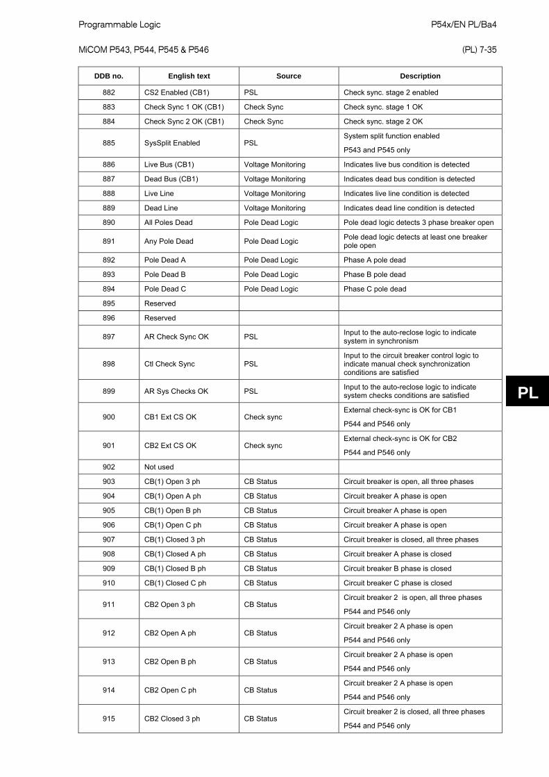
Programmable Logic P54x/EN PL/Ba4 MiCOM P543, P544, P545 & P546
(PL) 7-35
PL
DDB no. English text Source Description
882 CS2 Enabled (CB1) PSL Check sync. stage 2 enabled
883 Check Sync 1 OK (CB1) Check Sync Check sync. stage 1 OK
884 Check Sync 2 OK (CB1) Check Sync Check sync. stage 2 OK
885 SysSplit Enabled PSL System split function enabled
P543 and P545 only
886 Live Bus (CB1) Voltage Monitoring Indicates live bus condition is detected
887 Dead Bus (CB1) Voltage Monitoring Indicates dead bus condition is detected
888 Live Line Voltage Monitoring Indicates live line condition is detected
889 Dead Line Voltage Monitoring Indicates dead line condition is detected
890 All Poles Dead Pole Dead Logic Pole dead logic detects 3 phase breaker open
891 Any Pole Dead Pole Dead Logic Pole dead logic detects at least one breaker pole open
892 Pole Dead A Pole Dead Logic Phase A pole dead
893 Pole Dead B Pole Dead Logic Phase B pole dead
894 Pole Dead C Pole Dead Logic Phase C pole dead
895 Reserved
896 Reserved
897 AR Check Sync OK PSL Input to the auto-reclose logic to indicate system in synchronism
898 Ctl Check Sync PSL Input to the circuit breaker control logic to indicate manual check synchronization conditions are satisfied
899 AR Sys Checks OK PSL Input to the auto-reclose logic to indicate system checks conditions are satisfied
900 CB1 Ext CS OK Check sync External check-sync is OK for CB1
P544 and P546 only
901 CB2 Ext CS OK Check sync External check-sync is OK for CB2
P544 and P546 only
902 Not used
903 CB(1) Open 3 ph CB Status Circuit breaker is open, all three phases
904 CB(1) Open A ph CB Status Circuit breaker A phase is open
905 CB(1) Open B ph CB Status Circuit breaker A phase is open
906 CB(1) Open C ph CB Status Circuit breaker A phase is open
907 CB(1) Closed 3 ph CB Status Circuit breaker is closed, all three phases
908 CB(1) Closed A ph CB Status Circuit breaker A phase is closed
909 CB(1) Closed B ph CB Status Circuit breaker B phase is closed
910 CB(1) Closed C ph CB Status Circuit breaker C phase is closed
911 CB2 Open 3 ph CB Status Circuit breaker 2 is open, all three phases
P544 and P546 only
912 CB2 Open A ph CB Status Circuit breaker 2 A phase is open
P544 and P546 only
913 CB2 Open B ph CB Status Circuit breaker 2 A phase is open
P544 and P546 only
914 CB2 Open C ph CB Status Circuit breaker 2 A phase is open
P544 and P546 only
915 CB2 Closed 3 ph CB Status Circuit breaker 2 is closed, all three phases
P544 and P546 only
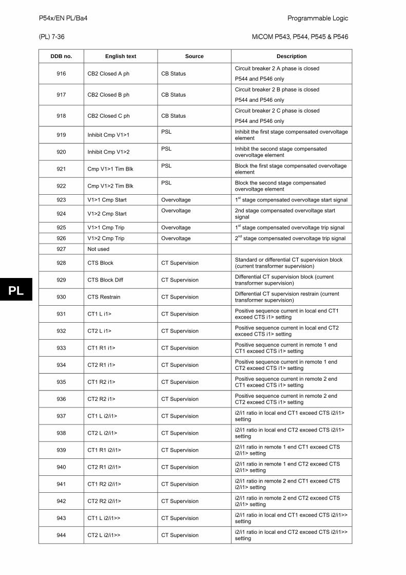
P54x/EN PL/Ba4 Programmable Logic
(PL) 7-36
MiCOM P543, P544, P545 & P546
PL
DDB no. English text Source Description
916 CB2 Closed A ph CB Status Circuit breaker 2 A phase is closed
P544 and P546 only
917 CB2 Closed B ph CB Status Circuit breaker 2 B phase is closed
P544 and P546 only
918 CB2 Closed C ph CB Status Circuit breaker 2 C phase is closed
P544 and P546 only
919 Inhibit Cmp V1>1 PSL Inhibit the first stage compensated overvoltage element
920 Inhibit Cmp V1>2 PSL Inhibit the second stage compensated overvoltage element
921 Cmp V1>1 Tim Blk PSL Block the first stage compensated overvoltage element
922 Cmp V1>2 Tim Blk PSL Block the second stage compensated overvoltage element
923 V1>1 Cmp Start Overvoltage 1st stage compensated overvoltage start signal
924 V1>2 Cmp Start Overvoltage 2nd stage compensated overvoltage start signal
925 V1>1 Cmp Trip Overvoltage 1st stage compensated overvoltage trip signal
926 V1>2 Cmp Trip Overvoltage 2nd stage compensated overvoltage trip signal
927 Not used
928 CTS Block CT Supervision Standard or differential CT supervision block (current transformer supervision)
929 CTS Block Diff CT Supervision Differential CT supervision block (current transformer supervision)
930 CTS Restrain CT Supervision Differential CT supervision restrain (current transformer supervision)
931 CT1 L i1> CT Supervision Positive sequence current in local end CT1 exceed CTS i1> setting
932 CT2 L i1> CT Supervision Positive sequence current in local end CT2 exceed CTS i1> setting
933 CT1 R1 i1> CT Supervision Positive sequence current in remote 1 end CT1 exceed CTS i1> setting
934 CT2 R1 i1> CT Supervision Positive sequence current in remote 1 end CT2 exceed CTS i1> setting
935 CT1 R2 i1> CT Supervision Positive sequence current in remote 2 end CT1 exceed CTS i1> setting
936 CT2 R2 i1> CT Supervision Positive sequence current in remote 2 end CT2 exceed CTS i1> setting
937 CT1 L i2/i1> CT Supervision i2/i1 ratio in local end CT1 exceed CTS i2/i1> setting
938 CT2 L i2/i1> CT Supervision i2/i1 ratio in local end CT2 exceed CTS i2/i1> setting
939 CT1 R1 i2/i1> CT Supervision i2/i1 ratio in remote 1 end CT1 exceed CTS i2/i1> setting
940 CT2 R1 i2/i1> CT Supervision i2/i1 ratio in remote 1 end CT2 exceed CTS i2/i1> setting
941 CT1 R2 i2/i1> CT Supervision i2/i1 ratio in remote 2 end CT1 exceed CTS i2/i1> setting
942 CT2 R2 i2/i1> CT Supervision i2/i1 ratio in remote 2 end CT2 exceed CTS i2/i1> setting
943 CT1 L i2/i1>> CT Supervision i2/i1 ratio in local end CT1 exceed CTS i2/i1>> setting
944 CT2 L i2/i1>> CT Supervision i2/i1 ratio in local end CT2 exceed CTS i2/i1>> setting
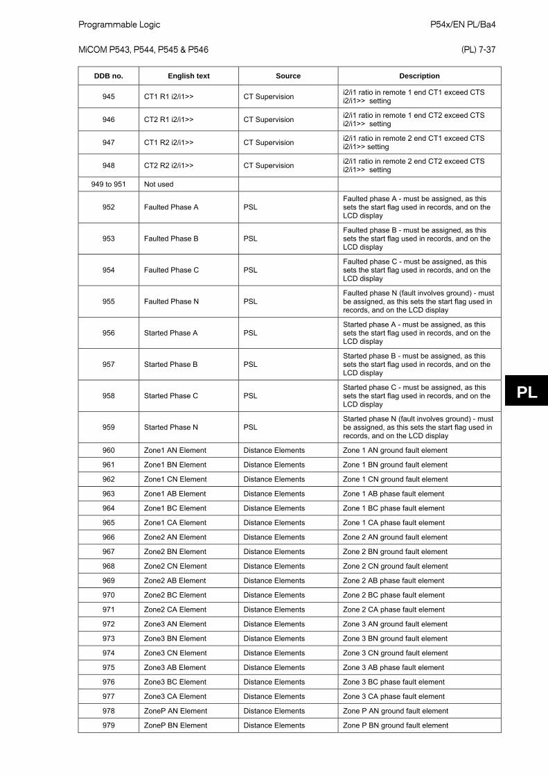
Programmable Logic P54x/EN PL/Ba4 MiCOM P543, P544, P545 & P546
(PL) 7-37
PL
DDB no. English text Source Description
945 CT1 R1 i2/i1>> CT Supervision i2/i1 ratio in remote 1 end CT1 exceed CTS i2/i1>> setting
946 CT2 R1 i2/i1>> CT Supervision i2/i1 ratio in remote 1 end CT2 exceed CTS i2/i1>> setting
947 CT1 R2 i2/i1>> CT Supervision i2/i1 ratio in remote 2 end CT1 exceed CTS i2/i1>> setting
948 CT2 R2 i2/i1>> CT Supervision i2/i1 ratio in remote 2 end CT2 exceed CTS i2/i1>> setting
949 to 951 Not used
952 Faulted Phase A PSL Faulted phase A - must be assigned, as this sets the start flag used in records, and on the LCD display
953 Faulted Phase B PSL Faulted phase B - must be assigned, as this sets the start flag used in records, and on the LCD display
954 Faulted Phase C PSL Faulted phase C - must be assigned, as this sets the start flag used in records, and on the LCD display
955 Faulted Phase N PSL Faulted phase N (fault involves ground) - must be assigned, as this sets the start flag used in records, and on the LCD display
956 Started Phase A PSL Started phase A - must be assigned, as this sets the start flag used in records, and on the LCD display
957 Started Phase B PSL Started phase B - must be assigned, as this sets the start flag used in records, and on the LCD display
958 Started Phase C PSL Started phase C - must be assigned, as this sets the start flag used in records, and on the LCD display
959 Started Phase N PSL Started phase N (fault involves ground) - must be assigned, as this sets the start flag used in records, and on the LCD display
960 Zone1 AN Element Distance Elements Zone 1 AN ground fault element
961 Zone1 BN Element Distance Elements Zone 1 BN ground fault element
962 Zone1 CN Element Distance Elements Zone 1 CN ground fault element
963 Zone1 AB Element Distance Elements Zone 1 AB phase fault element
964 Zone1 BC Element Distance Elements Zone 1 BC phase fault element
965 Zone1 CA Element Distance Elements Zone 1 CA phase fault element
966 Zone2 AN Element Distance Elements Zone 2 AN ground fault element
967 Zone2 BN Element Distance Elements Zone 2 BN ground fault element
968 Zone2 CN Element Distance Elements Zone 2 CN ground fault element
969 Zone2 AB Element Distance Elements Zone 2 AB phase fault element
970 Zone2 BC Element Distance Elements Zone 2 BC phase fault element
971 Zone2 CA Element Distance Elements Zone 2 CA phase fault element
972 Zone3 AN Element Distance Elements Zone 3 AN ground fault element
973 Zone3 BN Element Distance Elements Zone 3 BN ground fault element
974 Zone3 CN Element Distance Elements Zone 3 CN ground fault element
975 Zone3 AB Element Distance Elements Zone 3 AB phase fault element
976 Zone3 BC Element Distance Elements Zone 3 BC phase fault element
977 Zone3 CA Element Distance Elements Zone 3 CA phase fault element
978 ZoneP AN Element Distance Elements Zone P AN ground fault element
979 ZoneP BN Element Distance Elements Zone P BN ground fault element

P54x/EN PL/Ba4 Programmable Logic
(PL) 7-38
MiCOM P543, P544, P545 & P546
PL
DDB no. English text Source Description
980 ZoneP CN Element Distance Elements Zone P CN ground fault element
981 ZoneP AB Element Distance Elements Zone P AB phase fault element
982 ZoneP BC Element Distance Elements Zone P BC phase fault element
983 ZoneP CA Element Distance Elements Zone P CA phase fault element
984 Zone4 AN Element Distance Elements Zone 4 AN ground fault element
985 Zone4 BN Element Distance Elements Zone 4 BN ground fault element
986 Zone4 CN Element Distance Elements Zone 4 CN ground fault element
987 Zone4 AB Element Distance Elements Zone 4 AB phase fault element
988 Zone4 BC Element Distance Elements Zone 4 BC phase fault element
989 Zone4 CA Element Distance Elements Zone 4 CA phase fault element
990 to 995 Not used
996 DEF Forward Directional Earth Fault DEF forward (directional earth fault aided scheme detector)
997 DEF Reverse Directional Earth Fault DEF reverse (directional earth fault aided scheme detector)
998 Delta Dir FWD AN Delta Directional Element Delta directional scheme forward AN detection
999 Delta Dir FWD BN Delta Directional Element Delta directional scheme forward BN detection
1000 Delta Dir FWD CN Delta Directional Element Delta directional scheme forward CN detection
1001 Delta Dir FWD AB Delta Directional Element Delta directional scheme forward AB detection
1002 Delta Dir FWD BC Delta Directional Element Delta directional scheme forward BC detection
1003 Delta Dir FWD CA Delta Directional Element Delta directional scheme forward CA detection
1004 Delta Dir Rev AN Delta Directional Element Delta directional scheme reverse AN detection
1005 Delta Dir Rev BN Delta Directional Element Delta directional scheme reverse BN detection
1006 Delta Dir Rev CN Delta Directional Element Delta directional scheme reverse CN detection
1007 Delta Dir Rev AB Delta Directional Element Delta directional scheme reverse AB detection
1008 Delta Dir Rev BC Delta Directional Element Delta directional scheme reverse BC detection
1009 Delta Dir Rev CA Delta Directional Element Delta directional scheme reverse CA detection
1010 Phase Select A Phase Selector Phase selector - phase A pickup
1011 Phase Select B Phase Selector Phase selector - phase B pickup
1012 Phase Select C Phase Selector Phase selector - phase C pickup
1013 Phase Select N Phase Selector Phase selector - neutral indication
1014 P Swing Detector Powerswing Blocking Power swing detected
1015 PSB Fault Powerswing Blocking Power swing block fault
1016 I(2)/I(1)> A Inrush Detector
2nd harmonic current ratio exceeds threshold on phase A (may be used to block any instantaneous distance elements that reach through the reactance of a power transformer)
1017 I(2)/I(1)> B Inrush Detector
2nd harmonic current ratio exceeds threshold on phase B (may be used to block any instantaneous distance elements that reach through the reactance of a power transformer)
1018 I(2)/I(1)> C Inrush Detector
2nd harmonic current ratio exceeds threshold on phase C (may be used to block any instantaneous distance elements that reach through the reactance of a power transformer)
1019 I(2)/I(1)> N Inrush Detector
2nd harmonic current ratio exceeds threshold on neutral current measurement (may be used to block any instantaneous distance elements that reach through the reactance of a power transformer)

Programmable Logic P54x/EN PL/Ba4 MiCOM P543, P544, P545 & P546
(PL) 7-39
PL
DDB no. English text Source Description
1020 Clear Stats Cmd PSL
This is an indication of the command “Clear Statistics” available in the PSL. This DDB could be used to reset statistics at the remote end (via IM64) by linking it to DDB 544 - clear statistics - at the remote end
1021 to 1023 Not used
1024 LED1 Red Output Conditioner Programmable LED 1 red is energized
1025 LED1 Grn. Output Conditioner Programmable LED 1 green is energized
1038 LED8 Red Output Conditioner Programmable LED 8 red is energized
1039 LED8 Grn. Output Conditioner Programmable LED 8 green is energized
1040 FnKey LED1 Red Output Conditioner Programmable function key LED 1 red is energized
1041 FnKey LED1 Grn. Output Conditioner Programmable function key LED 1 green is energized
1058 FnKey LED10 Red Output Conditioner Programmable function key LED 10 red is energized
1059 FnKey LED10 Grn. Output Conditioner Programmable function key LED 10 green is energized
1060 LED1 Con R PSL Assignment of input signal to drive output LED 1 red
1061 LED1 Con G PSL Assignment of signal to drive output LED 1 green. To drive LED 1 yellow DDB 676 and DDB 677 must be driven at the same time
1074 LED8 Con R PSL Assignment of signal to drive output LED 8 red
1075 LED8 Con G PSL Assignment of signal to drive output LED 8 green. To drive LED 8 yellow DDB 690 and DDB 691 must be active at the same time
1076 FnKey LED1 ConR PSL Assignment of signal to drive output function key LED 1 red. This LED is associated with function key 1
1077 FnKey LED1 ConG PSL
Assignment of signal to drive output function key LED 1 green. This LED is associated with function key 1. To drive function key LED, yellow DDB 692 and DDB 693 must be active at the same time
1094 FnKey LED10 ConR PSL Assignment of signal to drive output function key LED 10 red. This LED is associated with function key 10
1095 FnKey LED10 ConG PSL
Assignment of signal to drive output function key LED 10 green. This LED is associated with function key 10. To drive function key LED1 yellow, DDB 710 and DDB 711 must be active at the same time
1096 Function Key 1 Function Key Function key 1 is activated. In ‘Normal’ mode it is high on keypress and in ‘Toggle’ mode remains high/low on single keypress
1105 Function Key 10 Function Key Function key 10 is activated. In ‘Normal’ mode it is high on keypress and in ‘Toggle’ mode remains high/low on single keypress
1106 I^ Maint. Alarm (CB1) CB Monitoring Broken current maintenance alarm - circuit breaker cumulative duty alarm set-point
1107 I^ Lockout Alarm (CB1) CB Monitoring Broken current lockout alarm - circuit breaker cumulative duty has been exceeded
1108 CB OPs Maint. (CB1) CB Monitoring No of circuit breaker operations maintenance alarm - indicated due to circuit breaker trip operations threshold
1109 CB OPs Lockout (CB1) CB Monitoring No of circuit breaker operations maintenance lockout - excessive number of circuit breaker trip operations, safety lockout
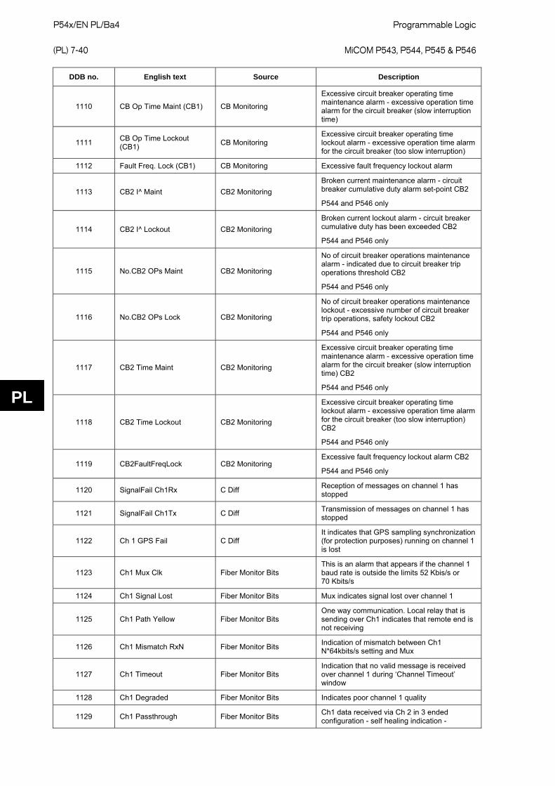
P54x/EN PL/Ba4 Programmable Logic
(PL) 7-40
MiCOM P543, P544, P545 & P546
PL
DDB no. English text Source Description
1110 CB Op Time Maint (CB1) CB Monitoring
Excessive circuit breaker operating time maintenance alarm - excessive operation time alarm for the circuit breaker (slow interruption time)
1111 CB Op Time Lockout (CB1) CB Monitoring
Excessive circuit breaker operating time lockout alarm - excessive operation time alarm for the circuit breaker (too slow interruption)
1112 Fault Freq. Lock (CB1) CB Monitoring Excessive fault frequency lockout alarm
1113 CB2 I^ Maint CB2 Monitoring Broken current maintenance alarm - circuit breaker cumulative duty alarm set-point CB2
P544 and P546 only
1114 CB2 I^ Lockout CB2 Monitoring Broken current lockout alarm - circuit breaker cumulative duty has been exceeded CB2
P544 and P546 only
1115 No.CB2 OPs Maint CB2 Monitoring
No of circuit breaker operations maintenance alarm - indicated due to circuit breaker trip operations threshold CB2
P544 and P546 only
1116 No.CB2 OPs Lock CB2 Monitoring
No of circuit breaker operations maintenance lockout - excessive number of circuit breaker trip operations, safety lockout CB2
P544 and P546 only
1117 CB2 Time Maint CB2 Monitoring
Excessive circuit breaker operating time maintenance alarm - excessive operation time alarm for the circuit breaker (slow interruption time) CB2
P544 and P546 only
1118 CB2 Time Lockout CB2 Monitoring
Excessive circuit breaker operating time lockout alarm - excessive operation time alarm for the circuit breaker (too slow interruption) CB2
P544 and P546 only
1119 CB2FaultFreqLock CB2 Monitoring Excessive fault frequency lockout alarm CB2
P544 and P546 only
1120 SignalFail Ch1Rx C Diff Reception of messages on channel 1 has stopped
1121 SignalFail Ch1Tx C Diff Transmission of messages on channel 1 has stopped
1122 Ch 1 GPS Fail C Diff It indicates that GPS sampling synchronization (for protection purposes) running on channel 1 is lost
1123 Ch1 Mux Clk Fiber Monitor Bits This is an alarm that appears if the channel 1 baud rate is outside the limits 52 Kbis/s or 70 Kbits/s
1124 Ch1 Signal Lost Fiber Monitor Bits Mux indicates signal lost over channel 1
1125 Ch1 Path Yellow Fiber Monitor Bits One way communication. Local relay that is sending over Ch1 indicates that remote end is not receiving
1126 Ch1 Mismatch RxN Fiber Monitor Bits Indication of mismatch between Ch1 N*64kbits/s setting and Mux
1127 Ch1 Timeout Fiber Monitor Bits Indication that no valid message is received over channel 1 during ‘Channel Timeout’ window
1128 Ch1 Degraded Fiber Monitor Bits Indicates poor channel 1 quality
1129 Ch1 Passthrough Fiber Monitor Bits Ch1 data received via Ch 2 in 3 ended configuration - self healing indication -

Programmable Logic P54x/EN PL/Ba4 MiCOM P543, P544, P545 & P546
(PL) 7-41
PL
DDB no. English text Source Description
1130 SignalFail Ch2Rx C Diff Reception of messages on channel 2 has stopped
1131 SignalFail Ch2Tx C Diff Transmission of messages on channel 1 has stopped
1132 Ch 2 GPS Fail C Diff It indicates that GPS sampling synchronization (for protection purposes) running on channel 2 is lost
1133 Ch2 Mux Clk Fiber Monitor Bits This is an alarm that appears if the channel 2 baud rate is outside the limits 52Kbis/s or 70 Kbits/s
1134 Ch2 Signal Lost Fiber Monitor Bits Mux indicates signal lost over channel 2
1135 Ch2 Path Yellow Fiber Monitor Bits One way communication. Local relay that is sending over Ch2 indicates that remote end is not receiving
1136 Ch2 Mismatch RxN Fiber Monitor Bits Indication of mismatch between InterMiCOM64 Ch 2 setting and Mux
1137 Ch2 Timeout Fiber Monitor Bits Indication that no valid message is received over channel 2 during ‘Channel Timeout’ window
1138 Ch2 Degraded Fiber Monitor Bits Indicates poor channel 2 quality
1139 Ch2 Passthrough Fiber Monitor Bits Ch2 data received via Ch 1 in 3 ended configuration - self healing indication -
1140 to 1148 Hidden
1149 F<1 Timer Block PSL Block Underfrequency Stage 1 Timer
1150 F<2 Timer Block PSL Block Underfrequency Stage 2 Timer
1151 F<3 Timer Block PSL Block Underfrequency Stage 3 Timer
1152 F<4 Timer Block PSL Block Underfrequency Stage 4 Timer
1153 F>1 Timer Block PSL Block Overfrequency Stage 1 Timer
1154 F>2 Timer Block PSL Block Overfrequency Stage 2 Timer
1155 F<1 Start Frequency Protection Under frequency Stage 1 Start
1156 F<2 Start Frequency Protection Under frequency Stage 2 Start
1157 F<3 Start Frequency Protection Under frequency Stage 3 Start
1158 F<4 Start Frequency Protection Under frequency Stage 4 Start
1159 F>1 Start Frequency Protection Over frequency Stage 1 Start
1160 F>2 Start Frequency Protection Over frequency Stage 2 Start
1161 F<1 Trip Frequency Protection Under frequency Stage 1 Trip
1162 F<2 Trip Frequency Protection Under frequency Stage 2 Trip
1163 F<3 Trip Frequency Protection Under frequency Stage 3 Trip
1164 F<4 Trip Frequency Protection Under frequency Stage 4 Trip
1165 F>1 Trip Frequency Protection Over frequency Stage 1 Trip
1166 F>2 Trip Frequency Protection Over frequency Stage 2 Trip
1167 Inhibit F<1 PSL Inhibit stage 1 Under frequency protection
1168 Inhibit F<2 PSL Inhibit stage 2 Under frequency protection
1169 Inhibit F<3 PSL Inhibit stage 3 Under frequency protection
1170 Inhibit F<4 PSL Inhibit stage 4 Under frequency protection
1171 Inhibit F>1 PSL Inhibit stage 1 Over frequency protection
1172 Inhibit F>2 PSL Inhibit stage 2 Over frequency protection
1173 to 1175 Not used

P54x/EN PL/Ba4 Programmable Logic
(PL) 7-42
MiCOM P543, P544, P545 & P546
PL
DDB no. English text Source Description
1176 HMI Access Lvl 1 It indicates that level access 1 for HMI interface is enabled
1177 HMI Access Lvl 2 It indicates that level access 2 for HMI interface is enabled
1178 FPort AccessLvl1 It indicates that level access 1 for the front port interface is enabled
1179 FPort AccessLvl2 It indicates that level access 2 for the front port interface is enabled
1180 RPrt1 AccessLvl1 It indicates that level access 1 for the rear port 1 interface is enabled
1181 RPrt1 AccessLvl2 It indicates that level access 2 for the rear port 1 interface is enabled
1182 RPrt2 AccessLvl1 It indicates that level access 1 for the rear port 2 interface is enabled
1183 RPrt2 AccessLvl2 It indicates that level access 2 for the rear port 2 interface is enabled
1184 Monitor Bit 1 Commissioning Test Monitor port signal 1 - allows mapped monitor signals to be mapped to disturbance recorder or contacts
1191 Monitor Bit 8 Commissioning Test Monitor port signal 8
1192 Hidden
1193 Not used
1194 PSL Int 1 PSL PSL internal node
1293 PSL Int 100 PSL PSL internal node
1294 VTS Ia> VT Supervision “VTS I> Inhibit “ setting has been exceeded in phase a
1295 VTS Ib> VT Supervision “VTS I> Inhibit “ setting has been exceeded in phase b
1296 VTS Ic> VT Supervision “VTS I> Inhibit “ setting has been exceeded in phase c
1297 VTS Va> VT Supervision Va has exceed 30 volts (drop off at 10 volts)
1298 VTS Vb> VT Supervision Vb has exceed 30 volts (drop off at 10 volts)
1299 VTS Vc> VT Supervision Vc has exceed 30 volts (drop off at 10 volts)
1300 VTS I2> VT Supervision “VTS I2> Inhibit “ setting has been exceeded
1301 VTS V2> VT Supervision V2 has exceed 10 volts
1302 VTS Ia delta> VT Supervision Superimposed phase a current has exceed 0.1In
1303 VTS Ib delta> VT Supervision Superimposed phase b current has exceed 0.1In
1304 VTS Ic delta> VT Supervision Superimposed phase c current has exceed 0.1In
1305 to 1363 Not used
1364 CB1 Pre-Lockout Output from CB1 monitoring logic
1363 to 1374 Not used
1375 Teleprotection Disturbed This is an output signal available in the PSL, that could be mapped to “C Diff Failure” for IEC870-5-103
1376 I>> Back Up Supervision
This applies only if distance primary FUN is selected (in IEC870-5-103)
This signal is ON if an overcurrent stage is selected to be enabled on VTS and distance is blocked by VTS

Programmable Logic P54x/EN PL/Ba4 MiCOM P543, P544, P545 & P546
(PL) 7-43
PL
DDB no. English text Source Description
1377 O/C Trip By VTS
This applies only if distance primary FUN is selected (in IEC870-5-103)
This signal is ON if DDB 1376 is ON and one of the overcurrent stages set to be enabled on VTS condition trips
1378 Teleprot Tx
This applies only if distance primary FUN is selected (in IEC870-5-103)
This is an output signal available in the PSL, which could be mapped to a signal send of one of the two teleprotection channels
1379 Teleprot Rx
This applies only if distance primary FUN is selected (in IEC870-5-103)
This is an output signal available in the PSL, which could be mapped to a signal receive of one of the two teleprotection channels
1380 Group Warning
This is an output signal available in the PSL, which can be mapped in IEC870-5-103 to a minor defect which does not shut down the main protection
1381 Group Alarm This is an output signal available in the PSL, which can be mapped in IEC870-5-103 to a major problem normally linked to the watchdog
1382 AR On Pulse This is an output signal available in the PSL, which can be mapped to enable AR via pulse
1383 AR OFF Pulse This is an output signal available in the PSL, which can be mapped to disable AR via pulse
1384 AR Enable This is an output signal available in the PSL, which can be mapped to enable AR
1385 AR In Service Auto-reclose in service
1386 MaxCh1 PropDelay Setting MaxCh 1 PropDelay has been exceeded
1387 MaxCh2 PropDelay Setting MaxCh 2 PropDelay has been exceeded
1388 MaxCh1 Tx-RxTime Setting MaxCh1 Tx-RxTime has been exceeded
1389 MaxCh2 Tx-RxTime Setting MaxCh2 Tx-RxTime has been exceeded
1390 to 1403 Not used
1404 VTS Blk Distance VTS Logic Signal from the VTS logic that can be used to block operation of the distance elements
1405 to 1407 Not used
1408 CB2 Lead Auto-reclose
If setting "Leader Select By:" = Opto, then preferred leader CB is CB1 if input DDB "CB2 LEAD" is low, or CB2 if DDB "CB2 LEAD" is high.
P544 and P546 only
1409 Follower AR 1P Auto-reclose
If setting "Foll AR Mode" = Opto, then if input DDB "FARSP" is high, the follower CB is enabled for single phase autoreclose, if "FARSP" is low, the follower CB is NOT enabled for single phase autoreclose.D2215
P544 and P546 only

P54x/EN PL/Ba4 Programmable Logic
(PL) 7-44
MiCOM P543, P544, P545 & P546
PL
DDB no. English text Source Description
1410 Follower AR 3P Auto-reclose
If setting "Foll AR Mode" = Opto, then if input DDB "FAR3P" is high, the follower CB is enabled for three phase autoreclose, if "FAR3P" is low, the follower CB is NOT enabled for three phase autoreclose.
P544 and P546 only
1411 CB2 AR 3p InProg Auto-reclose Autoreclose in progress CB2
P544 and P546 only
1412 En CB2 Independ Auto-reclose
DDB mapped in PSL from opto or comms input. A signal from an autoreclose scheme on an adjacent circuit having shared control of CB2, to allow the "Independent Follower time" to start. (see description for DDB "CB2 Indep Init A" or "CB2 Indep Init B" or "CB2 Indep Init C" ).
P544 and P546 only
1413 to 1416 Not used
1417 Ext Rst CB2 AROK PSL
DDB mapped in PSL from opto or comms input. This input DDB is used when required to reset any CB2 Successful Autoreclose" signal.
P544 and P546 only
1418 Ext Rst CB2Shots PSL
DDB mapped in PSL from opto or comms input. This input DDB is used when required to reset the CB2 cumulative "Shots" counters.
P544 and P546 only
1419 Rst CB2 CloseDly PSL
DDB mapped in PSL. Reset Manual CB2 Close Timer Delay (stop & reset Manual Close Delay time for closing CB2).
P544 and P546 only
1420 Inhibit AR PSL DDB mapped in PSL from opto or comms input. External signal to inhibit autoreclose.
P544 and P546 only
1421 Block CB2 AR PSL
DDB mapped in PSL from opto or comms input. External signal to force CB2 autoreclose to lockout.
P544 and P546 only
1422 Rst CB2 Lockout PSL
DDB mapped in PSL from opto or comms input. Reset Lockout Opto Input to reset CB2 Lockout state
P544 and P546 only
1423 MCB/VTS CS2 PSL
DDB mapped in PSL from opto input (Bus2 VT secondary MCB tripped or VT fail detected by external VTS scheme), or signal from host relay VTS scheme
P544 and P546 only
1424 Inhibit LB2 PSL DDB mapped in PSL from opto input (external signal to inhibit Live Bus 2 function)
P544 and P546 only
1425 Inhibit DB2 PSL DDB mapped in PSL from opto input (external signal to inhibit Dead Bus 2 function)
P544 and P546 only
1426 CB2 CS1 Enabled PSL
DDB mapped in PSL from opto input or logic DDBs (enable CS2-1 check synchronism function)
P544 and P546 only

Programmable Logic P54x/EN PL/Ba4 MiCOM P543, P544, P545 & P546
(PL) 7-45
PL
DDB no. English text Source Description
1427 CB2 CS2 Enabled PSL
DDB mapped in PSL from opto input or logic DDBs (enable CS2-2 check synchronism function)
P544 and P546 only
1428 CB2 In Service
Signal from CB In Service logic, indicating that CB2 is "In Service", i.e. can be initiated to autoreclose,
P544 and P546 only
1429 CB2 NoAR Autoreclose CB2 not available for autoreclose
P544 and P546 only
1430 Not used
1431 Leader CB2 Autoreclose CB2 set as leader
P544 and P546 only
1432 Follower CB1 Autoreclose CB1 set as follower
P544 and P546 only
1433 Follower CB2 Autoreclose CB2 set as follower
P544 and P546 only
1434 CB2 AR Init Autoreclose Indicates initiation of a CB2 autoreclose cycle
P544 and P546 only.
1435 CB2 ARIP Autoreclose CB2 autoreclose cycle in progress
P544 and P546 only
1436 Not used
1437 Test Trip CB2A Trip CB2 A Ph for test trip & AR
P544 and P546 only
1438 Test Trip CB2B Trip CB2 B Ph for test trip & AR
P544 and P546 only
1439 Test Trip CB2C Trip CB2 C Ph for test trip & AR
P544 and P546 only
1440 Not used
1441 CB2 Failed AR CB2 autoreclose failed due to persistent fault
P544 and P546 only
1442 DTOK CB2L 1P
Output DDB indicates conditions to enable CB2 lead single phase autoreclose dead time to run are satisfied
P544 and P546 only
1443 DTOK CB2L 3P
Output DDB indicates conditions to enable CB2 lead three phase autoreclose dead time to run are satisfied
P544 and P546 only
1444 CB2 3P DTime Indicates CB2 three phase autoreclose dead time running
P544 and P546 only
1445 En CB2 Follower Indicates conditions are satisfied to enable CB2 follower sequence
P544 and P546 only
1446 1P Follower Time Indicates a single pole autoreclose follower time is running (either CB)
P544 and P546 only

P54x/EN PL/Ba4 Programmable Logic
(PL) 7-46
MiCOM P543, P544, P545 & P546
PL
DDB no. English text Source Description
1447 3P Follower Time Indicates a three pole autoreclose follower time is running (either CB)
P544 and P546 only
1448 Auto Close CB2 Signal from autoreclose logic to initiate CB2 close via “CB2 CB Control”
P544 and P546 only
1449 Set CB2 Close Indicates a CB2 Auto Close signal has been issued
P544 and P546 only
1450 CB2 Control
Output DDB can be applied to inhibit CB2 reclose by adjacent scheme until local autoreclose scheme confirms it is OK to close CB2
P544 and P546 only
1451 CB2 Succ 1P AR CB2 successful single phase AR
P544 and P546 only
1452 CB2 Succ 3P AR CB2 successful three phase AR
P544 and P546 only
1453 CB2 Close inProg CB2 Manual Close initiated – awaiting Man Close Delay time
P544 and P546 only
1454 CB2 Fast SCOK OK to reclose CB2 with sync check without waiting for dead time to complete
P544 and P546 only
1455 CB2L SCOK System conditions OK to reclose CB2 as leader when dead time complete
P544 and P546 only
1456 CB2F SCOK System conditions OK to reclose CB2 when follower time complete
P544 and P546 only
1457 Not used
1458 CB2 Man SCOK System conditions OK to manually close CB2
P544 and P546 only
1459 CB2 Fail Pr Trip signal to force CB2 AR lockout if CB2 fails to trip when protection operates
P544 and P546 only
1460 Not used
1461 Live Bus 2 Indicates Bus 2 input is live, i.e. voltage >= setting "Live Bus 2"
P544 and P546 only
1462 Dead Bus 2 Indicates Bus 2 input is dead i.e. voltage < setting "Dead Bus 2"
P544 and P546 only
1463 CB2 CS2 OK
CB2 close with synchronism check type 2 is permitted (setting CS2-2 = Enabled), and Line and Bus 2 voltages satisfy relay settings for CB2 synchronism check type 2
P544 and P546 only

Programmable Logic P54x/EN PL/Ba4 MiCOM P543, P544, P545 & P546
(PL) 7-47
PL
DDB no. English text Source Description
1464 CB1 CS2 SlipF>
Line-Bus 1 slip freq > SlipFr 1-2 setting (frequency difference (slip) between line voltage and bus 1 voltage is greater than maximum slip permitted for CB1 synchronism check type 2)
P544 and P546 only
1465 CB1 CS2 SlipF<
Line-Bus 1 slip freq < SlipFr 1-2 setting (frequency difference (slip) between line voltage and bus 1 voltage is within the permitted range for CB1 synchronism check type 2)
P544 and P546 only
1466 CB2 CS1 SlipF>
Line-Bus 2 slip freq > SlipFr 2-1 setting (frequency difference (slip) between line voltage and bus 2 voltage is greater than maximum slip permitted for CB2 synchronism check type 1)
P544 and P546 only
1467 CB2 CS1 SlipF<
Line-Bus 2 slip freq < SlipFr 2-1 setting (frequency difference (slip) between line voltage and bus 2 voltage is within the permitted range for CB2 synchronism check type 1)
P544 and P546 only
1468 CB2 CS2 SlipF>
Line-Bus 2 slip freq > SlipFr 2-2 setting (frequency difference (slip) between line voltage and bus 2 voltage is greater than maximum slip permitted for CB2 synchronism check type 2)
P544 and P546 only
1469 CB2 CS2 SlipF<
Line-Bus 2 slip freq < SlipFr 2-2 setting (frequency difference (slip) between line voltage and bus 2 voltage is within the permitted range for CB2 synchronism check type 2)
P544 and P546 only
1470 CB2 CS1 VL>VB
Voltage magnitude difference between Line V and Bus2 V is greater than setting "VDiff2-1" (line V > Bus V)
P544 and P546 only
1471 CB2 CS2 VL>VB
Voltage magnitude difference between Line V and Bus2 V is greater than setting "VDiff2-1" (line V > Bus V)
P544 and P546 only
1472 CB2 CS1 VL<VB
Voltage magnitude difference between Line V and Bus2 V is greater than setting "VDiff2-1" (line V < Bus V)
P544 and P546 only
1473 CB2 CS2 VL<VB
Voltage magnitude difference between Line V and Bus2 V is greater than setting "VDiff2-1" (line V < Bus V)
P544 and P546 only
1474 CB2 CS1 FL>FB
Frequency difference between Line V and Bus2 V is greater than setting "SlipFr2-1" (line freq > Bus freq)
P544 and P546 only
1475 CB2 CS2 FL>FB Frequency difference between Line V and Bus2 V is greater than setting "SlipFr2-2" (line freq > Bus freq)+D2253

P54x/EN PL/Ba4 Programmable Logic
(PL) 7-48
MiCOM P543, P544, P545 & P546
PL
DDB no. English text Source Description
1476 CB2 CS1 FL<FB
Frequency difference between Line V and Bus2 V is greater than setting "SlipFr2-1" (line freq < Bus freq)
P544 and P546 only
1477 CB2 CS2 FL<FB
Frequency difference between Line V and Bus2 V is greater than setting "SlipFr2-2" (line freq < Bus freq)
P544 and P546 only
1478 CB2 CS1 AngHigh+ Line/Bus2 phase angle in range: +Angle 2-1 to +180deg (anticlockwise from Vbus)
P544 and P546 only
1479 CB2 CS1 AngHigh- Line/Bus2 phase angle in range: -Angle 2-1 to -180deg (clockwise from Vbus)
P544 and P546 only
1480 CB2 CS2 AngHigh+ Line/Bus2 phase angle in range: +Angle 2-2 to +180deg (anticlockwise from Vbus)
P544 and P546 only
1481 CB2 CS2 AngHigh- Line/Bus2 phase angle in range: -Angle 2-2 to -180deg (clockwise from Vbus)
P544 and P546 only
1482 CB2 CS AngRotACW
Line freq > (Bus2 freq + 0.001Hz) (Line voltage vector rotating anticlockwise relative to VBus2)
P544 and P546 only
1483 CB2 CS AngRotCW
Bus2 freq > (Line freq + 0.001Hz) (Line voltage vector rotating clockwise relative to VBus2)
P544 and P546 only
1484 SChksInactiveCB2
Output from CB2 system check logic: indicates system checks for CB2 are disabled (setting "System Checks CB2" = Disabled or global setting "System Checks" = Disabled)
P544 and P546 only
1485 AR Force CB2 3P Autoreclose
This DDB is set when the autoreclose logic has determined that single pole tripping/autoreclosing is not permitted for CB2. It can be applied in PSL when required to force trip conversion logic for internal and/or external protection to three phase trip mode for CB2.
P544 and P546 only
1486 Not used
1487 Not used
1488 En CB1 Follower Indicates conditions are satisfied to enable CB1 follower sequence
P544 and P546 only
1489 to 1492 Not used
1493 CB1 CS2 FL>FB
Frequency difference between Line V and Bus1 V is greater than setting "SlipFr1-2" (line freq > Bus freq)
P544 and P546 only
1494 CB1 CS2 FL<FB
Frequency difference between Line V and Bus1 V is greater than setting "SlipFr1-2" (line freq < Bus freq)
P544 and P546 only

Programmable Logic P54x/EN PL/Ba4 MiCOM P543, P544, P545 & P546
(PL) 7-49
PL
DDB no. English text Source Description
1495 CB1 CS2 AngHigh+ Line/Bus1 phase angle in range: +Angle 1-2 to +180deg (anticlockwise from Vbus)
P544 and P546 only
1496 CB1 CS2 AngHigh- Line/Bus1 phase angle in range: -Angle 1-2 to -180deg (clockwise from Vbus)
P544 and P546 only
1497 Lead AR 1P PSL
If setting "Lead AR Mode" = Opto, then if input DDB "LARSP" is high, the leader CB is enabled for single phase autoreclose, if "LARSP" is low, the leader CB is NOT enabled for single phase autoreclose.
P544 and P546 only
1498 Lead AR 3P PSL
If setting "Lead AR Mode" = Opto, then if input DDB "LAR3P" is high, the leader CB is enabled for three phase autoreclose, if "LAR3P" is low, the leader CB is NOT enabled for three phase autoreclose.
P544 and P546 only
1499 CB2 Trip AR MemA CB2 A Ph trip & AR initiation memory
P544 and P546 only
1500 CB2 Trip AR MemB CB2 B Ph trip & AR initiation memory
P544 and P546 only
1501 CB2 Trip AR MemC CB2 C Ph trip & AR initiation memory
P544 and P546 only
1502 to 1503 Not used
1504 Init APh AR Test PSL
DDB mapped in PSL from opto or comms input. Input high-low operation will initiate APh test trip & autoreclose cycle
P544 and P546 only
1505 Init BPh AR Test PSL
DDB mapped in PSL from opto or comms input. Input high-low operation will initiate BPh test trip & autoreclose cycle
P544 and P546 only
1506 Init CPh AR Test PSL
DDB mapped in PSL from opto or comms input. Input high-low operation will initiate CPh test trip & autoreclose cycle
P544 and P546 only
1507 Init 3P AR Test PSL
DDB mapped in PSL from opto or comms input. Input high-low operation will initiate 3Ph test trip & autoreclose cycle
P544 and P546 only
1508 Ext Fault APh PSL
DDB mapped in PSL from opto or comms input: indicates external protection operated for fault involving A phase
P544 and P546 only
1509 Ext Fault BPh PSL
DDB mapped in PSL from opto or comms input: indicates external protection operated for fault involving B phase
P544 and P546 only
1510 Ext Fault CPh PSL
DDB mapped in PSL from opto or comms input: indicates external protection operated for fault involving C phase
P544 and P546 only
1511 to 1516 Not used

P54x/EN PL/Ba4 Programmable Logic
(PL) 7-50
MiCOM P543, P544, P545 & P546
PL
DDB no. English text Source Description
1517 Ext Rst CB1 AROK PSL
DDB mapped in PSL from opto or comms input. This input DDB is used when required to reset any CB1 "Successful Autoreclose" signal.
P544 and P546 only
1518 Ext Rst CB1Shots PSL
DDB mapped in PSL from opto or comms input. This input DDB is used when required to reset the CB1 cumulative "Shots" counters.
P544 and P546 only
1519 to 1520 Not used
1521 MCB/VTS CS1 PSL
DDB mapped in PSL from opto input (Bus1 VT secondary MCB tripped or VT fail detected by external VTS scheme), or signal from host relay VTS scheme
P544 and P546 only
1522 Inhibit LL PSL DDB mapped in PSL from opto input (external signal to inhibit Live Line function)
P544 and P546 only
1523 Inhibit DL PSL DDB mapped in PSL from opto input (external signal to inhibit Dead Line function)
P544 and P546 only
1524 Inhibit LB1 PSL DDB mapped in PSL from opto input (external signal to inhibit Live Bus 1 function)
P544 and P546 only
1525 Inhibit DB1 PSL DDB mapped in PSL from opto input (external signal to inhibit Dead Bus 1 function)
P544 and P546 only
1526 CB1 In Service CB1 In Service (can be initiated for autoreclose)
P544 and P546 only
1527 Not used
1528 CB1 NoAR Autoreclose CB1 not available for autoreclose
P544 and P546 only
1529 Not used
1530 Leader CB1 Autoreclose CB1 set as leader
P544 and P546 only
1531 to 1534 Not used
1535 CB1 Trip AR MemA A Ph trip & AR initiation memory
P544 and P546 only
1536 CB1 Trip AR MemB B Ph trip & AR initiation memory
P544 and P546 only
1537 CB1 Trip AR MemC C Ph trip & AR initiation memory
P544 and P546 only
1538 to 1540 Not used
1541 AR Start Autoreclose Any AR initiation signal present
P544 and P546 only
1542 ARIP Autoreclose Any AR cycle in progress
P544 and P546 only
1543 CB1 AR Init Autoreclose CB1 AR cycle initiation
P544 and P546 only
Programmable Logic P54x/EN PL/Ba4 MiCOM P543, P544, P545 & P546
(PL) 7-51
PL
DDB no. English text Source Description
1544 CB1 ARIP Autoreclose CB1 AR cycle in progress
P544 and P546 only
1545 Not used
1546 SC Count>Shots Sequence counts greater than shots
P544 and P546 only
1547 Evolve 3Ph
Convert SPAR to 3PAR. DDB mapped to give 100ms pulse to CB1 Trip 3Ph and CB2 Trip 3Ph outputs
P544 and P546 only
1548 to 1549 Not used
1550 CB1 Failed AR CB1 AR failed due to persistent fault
P544 and P546 only
1551 DTOK All Enabling condition for any dead time
P544 and P546 only
1552 DTOK CB1L 1P required for CB1 lead SPAR D Time
P544 and P546 only
1553 DTOK CB1L 3P required for CB1 lead 3PAR D Time
P544 and P546 only
1554 1P DTime Single pole dead time in progress
P544 and P546 only
1555 OK Time 3P OK to start 3PAR dead time
P544 and P546 only
1556 3P DTime1 3Phase dead time 1 running
P544 and P546 only
1557 3P DTime2 3Phase dead time 2 running
P544 and P546 only
1558 3P DTime3 3Phase dead time 3 running
P544 and P546 only
1559 3P DTime4 3Phase dead time 4 running
P544 and P546 only
1560 CB1 3P DTime CB1 3PAR dead time running
P544 and P546 only
1561 1PF TComp Either CB SP follower time complete
P544 and P546 only
1562 3PF TComp Either CB 3P follower time complete
P544 and P546 only
1563 Indep 1PF TComp Either CB independent SP follower time complete
P544 and P546 only
1564 Indep 3PF TComp Either CB independent 3P follower time complete
P544 and P546 only
1565 Set CB1 Close DDB (Optional PSL mapping to indication)
P544 and P546 only
1566 CB1 Control Inhibits CB1 reclose by adjacent scheme
P544 and P546 only

P54x/EN PL/Ba4 Programmable Logic
(PL) 7-52
MiCOM P543, P544, P545 & P546
PL
DDB no. English text Source Description
1567 1P Reclaim Time Single Ph AR reclaim time running
P544 and P546 only
1568 1P Reclaim TComp Single Ph AR reclaim time complete
P544 and P546 only
1569 3P Reclaim Time Three Ph AR reclaim time running
P544 and P546 only
1570 3P Reclaim TComp Three Ph AR reclaim time complete
P544 and P546 only
1571 CB1 Succ 1P AR CB1 successful single phase AR
P544 and P546 only
1572 CB1 Fast SCOK OK to reclose CB1 with sync check without waiting for dead time to complete
P544 and P546 only
1573 CB1L SCOK System conditions OK to reclose CB1 when dead time complete
P544 and P546 only
1574 CB1 Man SCOK System conditions OK to manually close CB1
P544 and P546 only
1575 CB1 Fail Pr Trip signal to force CB1 AR lockout
P544 and P546 only
1576 Not used
1577 CB2 CS1 OK CS2-1 is enabled and Line and Bus 2 voltages meet CS2-1 settings
P544 and P546 only
1578 CB1 CS1 SlipF> Line-Bus 1 slip freq > SlipFr 1-1 setting
P544 and P546 only
1579 CB1 CS1 SlipF< Line-Bus 1 slip freq < SlipFr 1-1 setting
P544 and P546 only
1580 CS VLine< Line Volts < CS UV setting
P544 and P546 only
1581 CS VLine> Line Volts > CS OV setting
P544 and P546 only
1582 CS VBus1< Bus1 Volts < CS UV setting
P544 and P546 only
1583 CS VBus1> Bus1 Volts > CS OV setting
P544 and P546 only
1584 CS VBus2< Bus2 Volts < CS UV setting
P544 and P546 only
1585 CS VBus2> Bus2 Volts > CS OV setting
P544 and P546 only
1586 CB1 CS1 VL>VB Line V > (Bus1 V + [VDiff1-1])
P544 and P546 only
1587 CB1 CS2 VL>VB Line V > (Bus1 V + [VDiff1-2])
P544 and P546 only
1588 CB1 CS1 VL<VB Bus1 V > (Line V + [VDiff1-1])
P544 and P546 only
Programmable Logic P54x/EN PL/Ba4 MiCOM P543, P544, P545 & P546
(PL) 7-53
PL
DDB no. English text Source Description
1589 CB1 CS2 VL<VB Bus1 V > (Line V + [VDiff1-2])
P544 and P546 only
1590 CB1 CS1 FL>FB Line F > (Bus1 F + [SlipFr1-1])
P544 and P546 only
1591 CB1 CS1 FL<FB Bus1 F > (Line F + [SlipFr1-1])
P544 and P546 only
1592 CB1 CS1 AngHigh+ Line/Bus1 phase angle in range: +Angle 1-1 to +180deg
P544 and P546 only
1593 CB1 CS1 AngHigh- Line/Bus1 phase angle in range: -Angle 1-1 to -180deg
P544 and P546 only
1594 CB1 CS AngRotACW Line freq > (Bus1 freq + 0.001Hz) (CS1 Angle Rotating Anticlockwise)
P544 and P546 only
1595 CB1 CS AngRotCW Bus1 freq > (Line freq + 0.001Hz) (CS1 Angle Rotating Clockwise)
P544 and P546 only
1596 Not used
1597 Rst CB2 Data Rst CB2 All Val
P544 and P546 only
1598 CB2 Pre-Lockout Output from CB2 monitoring logic
1599 CB2 LO Alarm CB2 LO Alarm
P544 and P546 only
1600 CB2 Trip 3ph Trip Conversion Logic 3 Phase Trip 2
P544 and P546 only
1601 CB2 Trip OutputA Trip Conversion Logic A Phase Trip 2
P544 and P546 only
1602 CB2 Trip OutputB Trip Conversion Logic B Phase Trip 2
P544 and P546 only
1603 CB2 Trip OutputC Trip Conversion Logic C Phase Trip 2
P544 and P546 only
1604 Force 3PTrip CB2 PSL
External input via DDB to force host relay trip conversion logic to issue a three phase trip signal to CB2 for all faults
P544 and P546 only
1605 Enable AR CB2
External input via DDB to enable CB2, if "in service", to be initiated for autoreclosing by an AR initiation signal from protection. DDB input defaults to high if not mapped in PSL, so CB2 AR initiation is permitted.
P544 and P546 only
1606 Pole Discrep.CB2 PSL Pole Discrepancy
P544 and P546 only
1607 Pole Discrep.CB2 Pole discrepency Pole Discrepancy
P544 and P546 only
1608 CB2 Trip I/P 3Ph PSL Trip 3 Phase - Input to Trip Latching Logic
P544 and P546 only

P54x/EN PL/Ba4 Programmable Logic
(PL) 7-54
MiCOM P543, P544, P545 & P546
PL
DDB no. English text Source Description
1609 AR Enable CB1
External input via DDB mapped in PSL to enable CB1, if "in service", to be initiated for autoreclosing by an AR initiation signal from protection. DDB input defaults to high if not mapped in PSL, so CB1 AR initiation is permitted.
P544 and P546 only
1610 to 1791 Not used
1.8 Factory default programmable scheme logic
The following section details the default settings of the PSL.
The P54xmodel options are as follows:
Model Opto inputs Relay outputs
P543xxx?xxxxxxK 16 14
P543xxx#xxxxxxK 16 7 standard and 4 high break
P544xxx?xxxxxxK 16 14
P544xxx#xxxxxxK 16 7 standard and 4 high break
P545xxx?xxxxxxK 24 32
P545xxx#xxxxxxK 24 16 standard and 8 high break
P545xxx$xxxxxxK 32 32
P546xxx?xxxxxxK 24 32
P546xxx#xxxxxxK 24 16 standard and 8 high break
P546xxx£xxxxxxK 24 8 standard and 12 high break
Note: ? is for models with only standard output contacts = A, B, C, D, E, F, G, H, J, K, L, M or R.
# is for models with standard and high break contacts = S, T, U, V, W, X, Z, 0, 1, 2, 3, 4 or 5.
$ is for models with 32 opto inputs with standard and high break contacts = 8 or 9
£ is for models with standard and high break contacts = I, N, O, P, Q, 8, 9.
1.9 Logic input mappings
The default mappings for each of the opto-isolated inputs are as shown in the following table:
Opto-input number P543 relay text Function
1 Input L1 L1 Inhibit Diff
2 Input L2 L2 Interlock
3 Input L3 L3 Aid 1 Receive
4 Input L4 L4 Aid 1 COS/LGS
5 Input L5 L5 Reset LEDs
6 Input L6 L6 Ext Trip A
7 Input L7 L7 Ext Trip B

Programmable Logic P54x/EN PL/Ba4 MiCOM P543, P544, P545 & P546
(PL) 7-55
PL
Opto-input number P543 relay text Function
8 Input L8 L8 Ext Trip C
9 Input L9 L9 CB AuxA 52-B
10 Input L10 L10 CB AuxB 52-B
11 Input L11 L11 CB AuxC 52-B
12 Input L12 L12 MCB/VTS
13 Input L13 L13 CB Close Man
14 Input L14 L14 Reset Lckout
15 Input L15 L15 CB Healthy
16 Input L16 L16 BAR
Opto-input number P544 relay text Function
1 Input L1 L1 Inhibit Diff
2 Input L2 L2 Interlock
3 Input L3 L3 Aid 1 Receive
4 Input L4 L4 Aid 1 COS/LGS
5 Input L5 L5 Reset LEDs
6 Input L6 L6 CB2 AuxA 52-B
7 Input L7 L7 CB2 AuxB 52-B
8 Input L8 L8 CB2 AuxC 52-B
9 Input L9 L9 CB AuxA 52-B
10 Input L10 L10 CB AuxB 52-B
11 Input L11 L11 CB AuxC 52-B
12 Input L12 L12 MCB/VTS
13 Input L13 L13 CB1 CloseMan
14 Input L14 L14 CB2 CloseMan
15 Input L15 L15 Not Used
16 Input L16 L16 Stub Bus En
Opto-input number P545 relay text Function
1 Input L1 L1 Inhibit Diff
2 Input L2 L2 Interlock
3 Input L3 L3 Aid 1 Receive
4 Input L4 L4 Aid 1 COS/LGS
5 Input L5 L5 Reset LEDs
6 Input L6 L6 Ext Trip A
7 Input L7 L7 Ext Trip B
8 Input L8 L8 Ext Trip C

P54x/EN PL/Ba4 Programmable Logic
(PL) 7-56
MiCOM P543, P544, P545 & P546
PL
Opto-input number P545 relay text Function
9 Input L9 L9 CB AuxA 52-B
10 Input L10 L10 CB AuxB 52-B
11 Input L11 L11 CB AuxC 52-B
12 Input L12 L12 MCB/VTS
13 Input L13 L13 CB Close Man
14 Input L14 L14 Reset Lckout
15 Input L15 L15 CB Healthy
16 Input L16 L16 BAR
17 Input L17 L17 PIT
18 Input L18 L18 Prop Dly Eq
19 Input L19 L19 IM64 1
20 Input L20 L20 IM64 2
21 Input L21 L21 IM64 3
22 Input L22 L22 IM64 4
23 Input L23 L23 Not Used
24 Input L24 L24 Not Used
25 Input L25 L25 Not Used
26 Input L26 L26 Not Used
27 Input L27 L27 Not Used
28 Input L28 L28 Not Used
29 Input L29 L29 Not Used
30 Input L30 L30 Not Used
31 Input L31 L31 Not Used
32 Input L32 L32 Not Used
Opto-input number P546 relay text Function
1 Input L1 L1 Inhibit Diff
2 Input L2 L2 BAR
3 Input L3 L3 Aid 1 Receive
4 Input L4 L4 Aid 1 COS/LGS
5 Input L5 L5 Reset LEDs
6 Input L6 L6 CB2 AuxA 52-B
7 Input L7 L7 CB2 AuxB 52-B
8 Input L8 L8 CB2 AuxC 52-B
9 Input L9 L9 CB AuxA 52-B
10 Input L10 L10 CB AuxB 52-B
11 Input L11 L11 CB AuxC 52-B
12 Input L12 L12 MCB/VTS
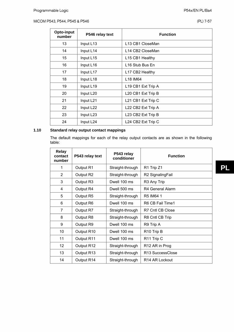
Programmable Logic P54x/EN PL/Ba4 MiCOM P543, P544, P545 & P546
(PL) 7-57
PL
Opto-input number P546 relay text Function
13 Input L13 L13 CB1 CloseMan
14 Input L14 L14 CB2 CloseMan
15 Input L15 L15 CB1 Healthy
16 Input L16 L16 Stub Bus En
17 Input L17 L17 CB2 Healthy
18 Input L18 L18 IM64
19 Input L19 L19 CB1 Ext Trip A
20 Input L20 L20 CB1 Ext Trip B
21 Input L21 L21 CB1 Ext Trip C
22 Input L22 L22 CB2 Ext Trip A
23 Input L23 L23 CB2 Ext Trip B
24 Input L24 L24 CB2 Ext Trip C
1.10 Standard relay output contact mappings
The default mappings for each of the relay output contacts are as shown in the following table:
Relay contact number
P543 relay text P543 relay conditioner Function
1 Output R1 Straight-through R1 Trip Z1
2 Output R2 Straight-through R2 SignalingFail
3 Output R3 Dwell 100 ms R3 Any Trip
4 Output R4 Dwell 500 ms R4 General Alarm
5 Output R5 Straight-through R5 IM64 1
6 Output R6 Dwell 100 ms R6 CB Fail Time1
7 Output R7 Straight-through R7 Cntl CB Close
8 Output R8 Straight-through R8 Cntl CB Trip
9 Output R9 Dwell 100 ms R9 Trip A
10 Output R10 Dwell 100 ms R10 Trip B
11 Output R11 Dwell 100 ms R11 Trip C
12 Output R12 Straight-through R12 AR in Prog
13 Output R13 Straight-through R13 SuccessClose
14 Output R14 Straight-through R14 AR Lockout

P54x/EN PL/Ba4 Programmable Logic
(PL) 7-58
MiCOM P543, P544, P545 & P546
PL
Relay contact number
P544 relay text P544 relay conditioner Function
1 Output R1 Straight-through R1 Trip Diff/Z1
2 Output R2 Straight-through R2 SignalingFail
3 Output R3 Dwell 100 ms R3 Any Trip
4 Output R4 Dwell 500 ms R4 General Alarm
5 Output R5 Straight-through R5 IM64 1
6 Output R6 Dwell 100 ms R6 CB1 Fail1Trip
7 Output R7 Straight-through R7 Cntl CB1 Close
8 Output R8 Straight-through R8 Cntl CB1 Trip
9 Output R9 Dwell 100 ms R9 Trip A
10 Output R10 Dwell 100 ms R10 Trip B
11 Output R11 Dwell 100 ms R11 Trip C
12 Output R12 Dwell 100 ms R12 CB2 Fail1Trip
13 Output R13 Straight-through R13 CntlCB2Close
14 Output R14 Straight-through R14 Cntl CB2Trip
Relay contact number
P545 relay text P545 relay conditioner Function
1 Output R1 Straight-through R1 Trip Z1
2 Output R2 Straight-through R2 SignalingFail
3 Output R3 Dwell 100 ms R3 Any Trip
4 Output R4 Dwell 500 ms R4 General Alarm
5 Output R5 Straight-through R5 IM64 1
6 Output R6 Dwell 100 ms R6 CB Fail Time1
7 Output R7 Straight-through R7 Cntl CB Close
8 Output R8 Straight-through R8 Cntl CB Trip
9 Output R9 Dwell 100 ms R9 Trip A
10 Output R10 Dwell 100 ms R10 Trip B
11 Output R11 Dwell 100 ms R11 Trip C
12 Output R12 Straight-through R12 AR in Prog
13 Output R13 Straight-through R13 SuccessClose
14 Output R14 Straight-through R14 AR Lockout
15 Output R15 Straight-through R15 AR InService
16 Output R16 Straight-through R16 BAR
17 Output R17 Dwell 100 ms R17 Trip A
18 Output R18 Dwell 100 ms R18 Trip B
19 Output R19 Dwell 100 ms R19 Trip C
20 Output R20 Straight-through R20 DistInst Trp

Programmable Logic P54x/EN PL/Ba4 MiCOM P543, P544, P545 & P546
(PL) 7-59
PL
Relay contact number
P545 relay text P545 relay conditioner Function
21 Output R21 Straight-through R21 Dist Dly Trp
22 Output R22 Straight-through R22 Aid DEF Trip
23 Output R23 Straight-through R23 Any Start
24 Output R24 Straight-through R24 Aid 1 Send
25 Output R25 Straight-through R25 GPS Fail
26 Output R26 Straight-through R26 Diff Trip
27 Output R27 Straight-through R27 VTS
28 Output R28 Straight-through R28 PSB
29 Output R29 Straight-through R29 IM64 2
30 Output R30 Straight-through R30 IM64 3
31 Output R31 Straight-through R31 IM64 4
32 Output R32 Straight-through R32 Not Used
Relay contact number
P546 relay text P546 relay conditioner Function
1 Output R1 Straight-through R1 Trip Z1
2 Output R2 Straight-through R2 SignalingFail
3 Output R3 Dwell 100 ms R3 Any Trip
4 Output R4 Dwell 500 ms R4 General Alarm
5 Output R5 Straight-through R5 IM64 1
6 Output R6 Dwell 100 ms R6 CB1 Fail1Trip
7 Output R7 Straight-through R7 Cntl CB1 Close
8 Output R8 Straight-through R8 Cntl CB1 Trip
9 Output R9 Dwell 100 ms R9 CB1 Trip A
10 Output R10 Dwell 100 ms R10 CB1 Trip B
11 Output R11 Dwell 100 ms R11 CB1 Trip C
12 Output R12 Dwell 100 ms R12 CB2 Fail1Trip
13 Output R13 Straight-through R13 CntlCB2Close
14 Output R14 Straight-through R14 Cntl CB2Trip
15 Output R15 Dwell 100 ms R15 CB1 Fail2Trip
16 Output R16 Dwell 100 ms R16 CB2 Fail2Trip
17 Output R17 Dwell 100 ms R17 CB2 Trip A
18 Output R18 Dwell 100 ms R18 CB2 Trip B
19 Output R19 Dwell 100 ms R19 CB2 Trip C
20 Output R20 Straight-through R20 DistInst Trp
21 Output R21 Straight-through R21 Dist Dly Trp
22 Output R22 Straight-through R22 Aid DEF Trip

P54x/EN PL/Ba4 Programmable Logic
(PL) 7-60
MiCOM P543, P544, P545 & P546
PL
Relay contact number
P546 relay text P546 relay conditioner Function
23 Output R23 Straight-through R23 Any Start
24 Output R24 Straight-through R24 Aid 1 Send
25 Output R25 Straight-through R25 GPS Fail
26 Output R26 Straight-through R26 Diff Trip
27 Output R27 Straight-through R27 VTS
28 Output R28 Straight-through R28 PSB
29 Output R29 Straight-through R29 AR CB1 Lockout
30 Output R30 Straight-through R30 AR CB2 Lockout
31 Output R31 Straight-through R31 ARIP
32 Output R32 Straight-through R32 SuccessClose
Note: A fault record can be generated by connecting one or a number of contacts to the Fault Record Trigger in PSL. It is recommended that the triggering contact be ‘self reset’ and not a latching. If a latching contact were chosen the fault record would not be generated until the contact had fully reset.
1.11 Optional high break relay output contact mappings
The default mappings for each of the standard and high break relay output contacts are as shown in the following table:
High break contacts are shown in grey shaded cells.
Relay contact number
P543 relay text P543 relay conditioner Function
1 Output R1 Straight-through R1 Trip Diff/Z1
2 Output R2 Straight-through R2 SignalingFail
3 Output R3 Dwell 100 ms R3 Any Trip
4 Output R4 Dwell 500 ms R4 General Alarm
5 Output R5 Straight-through R5 IM64 1
6 Output R6 Dwell 100 ms R6 CB Fail Time1
7 Output R7 Straight-through R7 Cntl CB Close
8 Output R8 Dwell 100 ms R8 Trip A
9 Output R9 Dwell 100 ms R9 Trip B
10 Output R10 Dwell 100 ms R10 Trip C
11 Output R11 Dwell 100 ms R11 Any Trip

Programmable Logic P54x/EN PL/Ba4 MiCOM P543, P544, P545 & P546
(PL) 7-61
PL
Relay contact number
P544 relay text P544 relay conditioner Function
1 Output R1 Straight-through R1 Trip Diff/Z1
2 Output R2 Straight-through R2 SignalingFail
3 Output R3 Dwell 100 ms R3 Any Trip
4 Output R4 Dwell 500 ms R4 General Alarm
5 Output R5 Straight-through R5 IM64 1
6 Output R6 Dwell 100 ms R6 CB1 Fail1Trip
7 Output R7 Straight-through R7 CB2 Fail1Trip
8 Output R8 Dwell 100 ms R8 Trip A
9 Output R9 Dwell 100 ms R9 Trip B
10 Output R10 Dwell 100 ms R10 Trip C
11 Output R11 Dwell 100 ms R11 Any Trip
Relay contact number
P545 relay text P545 relay conditioner Function
1 Output R1 Straight-through R1 Trip Z1 2 Output R2 Straight-through R2 SignalingFail 3 Output R3 Dwell 100 ms R3 Any Trip 4 Output R4 Dwell 500 ms R4 General Alarm 5 Output R5 Straight-through R5 IM64 1 6 Output R6 Dwell 100 ms R6 CB Fail Time1 7 Output R7 Straight-through R7 Cntl CB Close 8 Output R8 Straight-through R8 Cntl CB Trip 9 Output R9 Dwell 100 ms R9 Trip A 10 Output R10 Dwell 100 ms R10 Trip B 11 Output R11 Dwell 100 ms R11 Trip C 12 Output R12 Straight-through R12 AR in Prog 13 Output R13 Straight-through R13 SuccessClose 14 Output R14 Straight-through R14 AR Lockout 15 Output R15 Straight-through R15 AR InService 16 Output R16 Straight-through R16 Aid 1 Send 17 Output R17 Dwell 100 ms R17 Trip A 18 Output R18 Dwell 100 ms R18 Trip B 19 Output R19 Dwell 100 ms R19 Trip C 20 Output R20 Dwell 100 ms R20 Any Trip 21 Output R21 Dwell 100 ms R21 Trip A 22 Output R22 Dwell 100 ms R22 Trip B 23 Output R23 Dwell 100 ms R23 Trip C 24 Output R24 Dwell 100 ms R24 Any Trip

P54x/EN PL/Ba4 Programmable Logic
(PL) 7-62
MiCOM P543, P544, P545 & P546
PL
P546 with 16 standard outputs and 8 high break outputs (option S)
Relay contact number
P546 relay text P546 relay conditioner Function
1 Output R1 Straight-through R1 Trip Z1
2 Output R2 Straight-through R2 SignalingFail
3 Output R3 Dwell 100 ms R3 Any Trip
4 Output R4 Dwell 500 ms R4 General Alarm
5 Output R5 Straight-through R5 IM64 1
6 Output R6 Dwell 100 ms R6 CB1 Fail1Trip
7 Output R7 Straight-through R7 Cntl CB1 Close
8 Output R8 Straight-through R8 Cntl CB1 Trip
9 Output R9 Dwell 100 ms R9 CB1 Trip A
10 Output R10 Dwell 100 ms R10 CB1 Trip B
11 Output R11 Dwell 100 ms R11 CB1 Trip C
12 Output R12 Dwell 100 ms R12 Any Start
13 Output R13 Straight-through R13 CntlCB2Close
14 Output R14 Straight-through R14 Cntl CB2Trip
15 Output R15 Dwell 100 ms R15 CB2 Fail1Trip
16 Output R16 Dwell 100 ms R16 Aid 1 Send
17 Output R17 Dwell 100 ms R17 CB1 Trip A
18 Output R18 Dwell 100 ms R18 CB1 Trip B
19 Output R19 Dwell 100 ms R19 CB1 Trip C
20 Output R20 Dwell 100 ms R20 CB1 Trip 3ph
21 Output R21 Dwell 100 ms R21 CB2 Trip A
22 Output R22 Dwell 100 ms R22 CB2 Trip B
23 Output R23 Dwell 100 ms R23 CB2 Trip C
24 Output R24 Dwell 100 ms R24 CB2 Trip 3ph P546 with 8 standard outputs and 12 high break outputs
Relay contact number
P546 relay text P546 relay conditioner Function
1 Output R1 Straight-through R1 Trip Z1
2 Output R2 Straight-through R2 SignalingFail
3 Output R3 Dwell 100 ms R3 Any Trip
4 Output R4 Dwell 500 ms R4 General Alarm
5 Output R5 Straight-through R5 IM64 1
6 Output R6 Dwell 100 ms R6 CB1 Fail1Trip
7 Output R7 Straight-through R7 Cntl CB1 Close
8 Output R8 Straight-through R8 Cntl CB1 Trip

Programmable Logic P54x/EN PL/Ba4 MiCOM P543, P544, P545 & P546
(PL) 7-63
PL
Relay contact number
P546 relay text P546 relay conditioner Function
9 Output R9 Dwell 100 ms R9 CB1 Trip A
10 Output R10 Dwell 100 ms R10 CB1 Trip B
11 Output R11 Dwell 100 ms R11 CB1 Trip C
12 Output R12 Dwell 100 ms R12 CB2 Fail1Trip
13 Output R13 Dwell 100 ms R13 CntlCB2Close
14 Output R14 Dwell 100 ms R14 Cntl CB2Trip
15 Output R15 Dwell 100 ms R15 CB1 Fail2Trip
16 Output R16 Dwell 100 ms R16 CB2 Fail2Trip
17 Output R17 Dwell 100 ms R17 CB2 Trip A
18 Output R18 Dwell 100 ms R18 CB2 Trip B
19 Output R19 Dwell 100 ms R19 CB2 Trip C
20 Output R20 Dwell 100 ms R20 DistInst Trp
Note: A fault record can be generated by connecting one or a number of contacts to the “Fault Record Trigger” in PSL. It is recommended that the triggering contact be ‘self reset’ and not a latching. If a latching contact were chosen the fault record would not be generated until the contact had fully reset.
1.12 Programmable LED output mappings
The default mappings for each of the programmable LEDs are as shown in the following table:
LED number LED Input connection/text Latched P543 LED function indication
1 LED 1 Red Yes Diff Trip 2 LED 2 Red Yes Dist Inst Trip 3 LED 3 Red Yes Dist Delay Trip 4 LED 4 Red No Signaling Fail 5 LED 5 Red No Any Start 6 LED 6 Red No AR in Progress 7 LED 7 Red No AR Lockout 8 LED 8 Red No Test Loopback 9 FnKey LED1 Red No Not Mapped 10 FnKey LED2 Red No Not Mapped 11 FnKey LED3 Red No Not Mapped 12 FnKey LED4 Red No Not Mapped 13 FnKey LED5 Red No Not Mapped 14 FnKey LED6 Red No Not Mapped 15 FnKey LED7 Red No Not Mapped 16 FnKey LED8 Red No Not Mapped 17 FnKey LED9 Red No Not Mapped 18 FnKey LED10 Red No Not Mapped
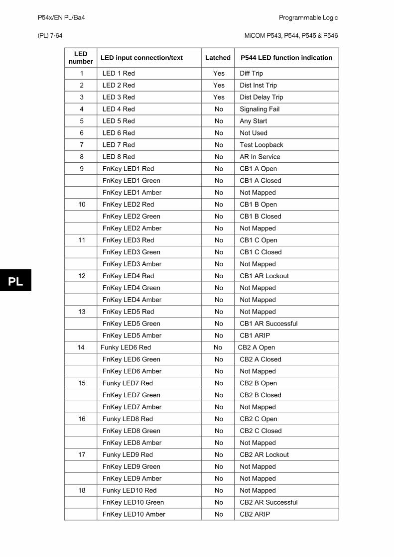
P54x/EN PL/Ba4 Programmable Logic
(PL) 7-64
MiCOM P543, P544, P545 & P546
PL
LED number LED input connection/text Latched P544 LED function indication
1 LED 1 Red Yes Diff Trip
2 LED 2 Red Yes Dist Inst Trip
3 LED 3 Red Yes Dist Delay Trip
4 LED 4 Red No Signaling Fail
5 LED 5 Red No Any Start
6 LED 6 Red No Not Used
7 LED 7 Red No Test Loopback
8 LED 8 Red No AR In Service
9 FnKey LED1 Red No CB1 A Open
FnKey LED1 Green No CB1 A Closed
FnKey LED1 Amber No Not Mapped
10 FnKey LED2 Red No CB1 B Open
FnKey LED2 Green No CB1 B Closed
FnKey LED2 Amber No Not Mapped
11 FnKey LED3 Red No CB1 C Open
FnKey LED3 Green No CB1 C Closed
FnKey LED3 Amber No Not Mapped
12 FnKey LED4 Red No CB1 AR Lockout
FnKey LED4 Green No Not Mapped
FnKey LED4 Amber No Not Mapped
13 FnKey LED5 Red No Not Mapped
FnKey LED5 Green No CB1 AR Successful
FnKey LED5 Amber No CB1 ARIP
14 Funky LED6 Red No CB2 A Open
FnKey LED6 Green No CB2 A Closed
FnKey LED6 Amber No Not Mapped
15 Funky LED7 Red No CB2 B Open
FnKey LED7 Green No CB2 B Closed
FnKey LED7 Amber No Not Mapped
16 Funky LED8 Red No CB2 C Open
FnKey LED8 Green No CB2 C Closed
FnKey LED8 Amber No Not Mapped
17 Funky LED9 Red No CB2 AR Lockout
FnKey LED9 Green No Not Mapped
FnKey LED9 Amber No Not Mapped
18 Funky LED10 Red No Not Mapped
FnKey LED10 Green No CB2 AR Successful
FnKey LED10 Amber No CB2 ARIP

Programmable Logic P54x/EN PL/Ba4 MiCOM P543, P544, P545 & P546
(PL) 7-65
PL
LED number LED input connection/text Latched P545 LED function indication
1 LED 1 Red Yes Diff Trip
2 LED 2 Red Yes Dist Inst Trip
3 LED 3 Red Yes Dist Delay Trip
4 LED 4 Red No Signaling Fail
5 LED 5 Red No Any Start
6 LED 6 Red No AR in Progress
7 LED 7 Red No AR Lockout
8 LED 8 Red No Test Loopback
9 Funky LED1 Red No Not Mapped
10 Funky LED2 Red No Not Mapped
11 Funky LED3 Red No Not Mapped
12 Funky LED4 Red No Not Mapped
13 Funky LED5 Red No Not Mapped
14 Funky LED6 Red No Not Mapped
15 Funky LED7 Red No Not Mapped
16 Funky LED8 Red No Not Mapped
17 Funky LED9 Red No Not Mapped
18 Funky LED10 Red No Not Mapped
1 LED 1 Red Yes Diff Trip
2 LED 2 Red Yes Dist Inst Trip
3 LED 3 Red Yes Dist Delay Trip
4 LED 4 Red No Signaling Fail
5 LED 5 Red No Any Start
6 LED 6 Red No Not Used
7 LED 7 Red No Test Loopback
8 LED 8 Red No AR In Service
9 Funky LED1 Red No CB1 A Open
FnKey LED1 Green No CB1 A Closed
FnKey LED1 Amber No Not Mapped
10 Funky LED2 Red No CB1 B Open
FnKey LED2 Green No CB1 B Closed
FnKey LED2 Amber No Not Mapped
11 Funky LED3 Red No CB1 C Open
FnKey LED3 Green No CB1 C Closed
FnKey LED3 Amber No Not Mapped
12 Funky LED4 Red No CB1 AR Lockout
FnKey LED4 Green No Not Mapped
FnKey LED4 Amber No Not Mapped

P54x/EN PL/Ba4 Programmable Logic
(PL) 7-66
MiCOM P543, P544, P545 & P546
PL
LED number LED input connection/text Latched P545 LED function indication
13 Funky LED5 Red No Not Mapped
FnKey LED5 Green No CB1 AR Successful
FnKey LED5 Amber No CB1 ARIP
14 Funky LED6 Red No CB2 A Open
FnKey LED6 Green No CB2 A Closed
FnKey LED6 Amber No Not Mapped
15 Funky LED7 Red No CB2 B Open
FnKey LED7 Green No CB2 B Closed
FnKey LED7 Amber No Not Mapped
16 Funky LED8 Red No CB2 C Open
FnKey LED8 Green No CB2 C Closed
FnKey LED8 Amber No Not Mapped
17 Funky LED9 Red No CB2 AR Lockout
FnKey LED9 Green No Not Mapped
FnKey LED9 Amber No Not Mapped
18 Funky LED10 Red No Not Mapped
FnKey LED10 Green No CB2 AR Successful
FnKey LED10 Amber No CB2 ARIP
1.13 Fault recorder start mappings
The default mappings for the signal which initiates a fault record is as shown in the following table:
Initiating Signal Fault Trigger
DDB Any Trip (522) Initiate fault recording from main protection trip
1.14 PSL DATA column
The MiCOM P54x relay contains a PSL DATA column that can be used to track PSL modifications. A total of 12 cells are contained in the PSL DATA column, 3 for each setting group. The function for each cell is shown below:
Grp. PSL Ref.
When downloading a PSL to the relay, the user will be prompted to enter which group the PSL is for and a reference identifier. The first 32 characters of the reference ID will be displayed in this cell. The and keys can be used to scroll through 32 characters as only 16 can be displayed at any one time.
18 Nov 2002
08:59:32.047
This cell displays the date and time when the PSL was down loaded to the relay.
Grp. 1 PSL
ID - 2062813232
This is a unique number for the PSL that has been entered. Any change in the PSL will result in a different number being displayed.
Note: The above cells are repeated for each setting group.
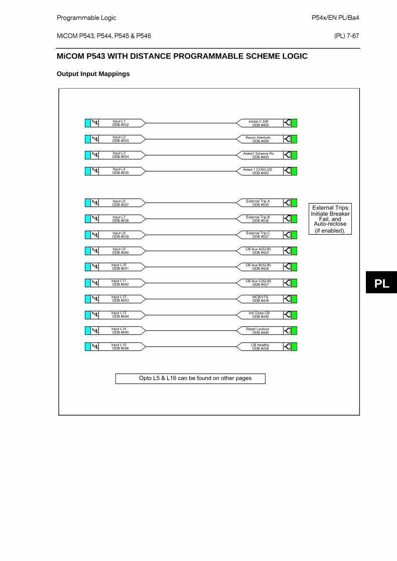
Programmable Logic P54x/EN PL/Ba4 MiCOM P543, P544, P545 & P546
(PL) 7-67
PL
MiCOM P543 WITH DISTANCE PROGRAMMABLE SCHEME LOGIC
Output Input Mappings
DDB #032Input L1
DDB #033Input L2
DDB #034Input L3
DDB #035Input L4
DDB #037Input L6
DDB #038Input L7
DDB #039Input L8
DDB #040Input L9
DDB #041Input L10
DDB #042Input L11
DDB #043Input L12
DDB #044Input L13
DDB #045Input L14
DDB #046Input L15
DDB #455Inhibit C Diff
DDB #456Recon Interlock
DDB #493Aided1 Scheme Rx
DDB #492Aided 1 COS/LGS
DDB #535External Trip A
DDB #536External Trip B
DDB #537External Trip C
DDB #425CB Aux A(52-B)
DDB #426CB Aux B(52-B)
DDB #427CB Aux C(52-B)
DDB #438MCB/VTS
DDB #440Init Close CB
DDB #446Reset Lockout
DDB #436CB Healthy
External Trips: Initiate Breaker
Fail, and Auto-reclose (if enabled).
Opto L5 & L16 can be found on other pages
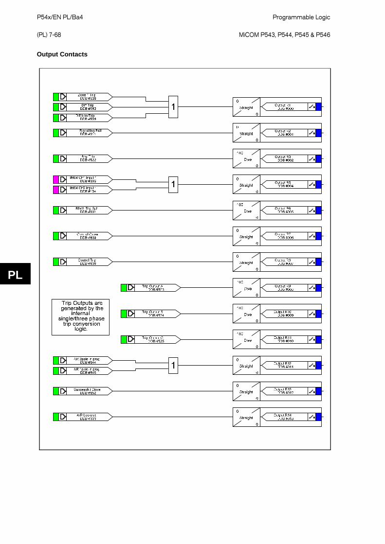
P54x/EN PL/Ba4 Programmable Logic
(PL) 7-68
MiCOM P543, P544, P545 & P546
PL
Output Contacts

Programmable Logic P54x/EN PL/Ba4 MiCOM P543, P544, P545 & P546
(PL) 7-69
PL
Output Contacts

P54x/EN PL/Ba4 Programmable Logic
(PL) 7-70
MiCOM P543, P544, P545 & P546
PL
LEDs
DDB #522Any Trip
DDB #702Fault REC TRIG
DDB #582Diff Trip
DDB #291Test Loopback
DDB #306A/R Lockout
DDB #844AR 3pole in prog
DDB #845AR 1pole in prog 1
1
1
DDB #608Zone 1 Trip
DDB #503Aid 1 Dist Trip
DDB #519Aid 2 Dist Trip
DDB #613Zone 2 Trip
DDB #618Zone 3 Trip
DDB #623Zone P Trip
DDB #628Zone 4 Trip
DDB #311Signalling Fail
DDB #1024LatchingLED1 Red
DDB #1025LED1 Grn
DDB #1026LatchingLED2 Red
DDB #1027LED2 Grn
DDB #1028LatchingLED3 Red
DDB #1029LED3 Grn
DDB #1030Non -Latching
LED4 Red
DDB #1031LED4 Grn
DDB #1034Non -Latching
LED6 Red
DDB #1035LED6 Grn
DDB #1036Non -Latching
LED7 Red
DDB #1037LED7 Grn
DDB #1038Non -Latching
LED8 Red
DDB #1039LED8 Grn
1DDB #586
Diff InterTrip
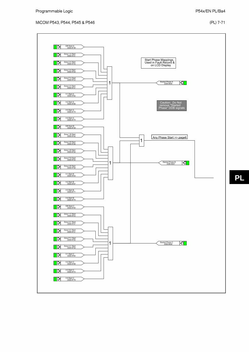
Programmable Logic P54x/EN PL/Ba4 MiCOM P543, P544, P545 & P546
(PL) 7-71
PL
DDB #741Zone 1 A Start
DDB #745Zone 2 A Start
DDB #749Zone 3 A Start
DDB #753Zone P A Start
DDB #757Zone 4 A Start
DDB #762I>1 Start A
DDB #766I>2 Start A
1
DDB #770I>3 Start A
DDB #774I>4 Start A
DDB #742Zone 1 B Start
DDB #746Zone 2 B Start
DDB #750Zone 3 B Start
DDB #754Zone P B Start
DDB #758Zone 4 B Start
DDB #763I>1 Start B
DDB #767I>2 Start B
DDB #771I>3 Start B
DDB #775I>4 Start B
1
DDB #743Zone 1 C Start
DDB #747Zone 2 C Start
DDB #751Zone 3 C Start
DDB #755Zone P C Start
DDB #759Zone 4 C Start
DDB #764I>1 Start C
DDB #768I>2 Start C
DDB #772I>3 Start C
DDB #776I>4 Start C
1
DDB #956Started Phase A
1Any Phase Start >> page6
DDB #957Started Phase B
DDB #958Started Phase C
DDB #738Diff Start A
DDB #739Diff Start B
DDB #740Diff Start C
Any Phase Start >> page6Any Phase Start >> page6
Start Phase Mappings. Used in Fault Record &
on LCD Display
Caution: Do Not remove "Started
Phase" DDB signals

P54x/EN PL/Ba4 Programmable Logic
(PL) 7-72
MiCOM P543, P544, P545 & P546
PL
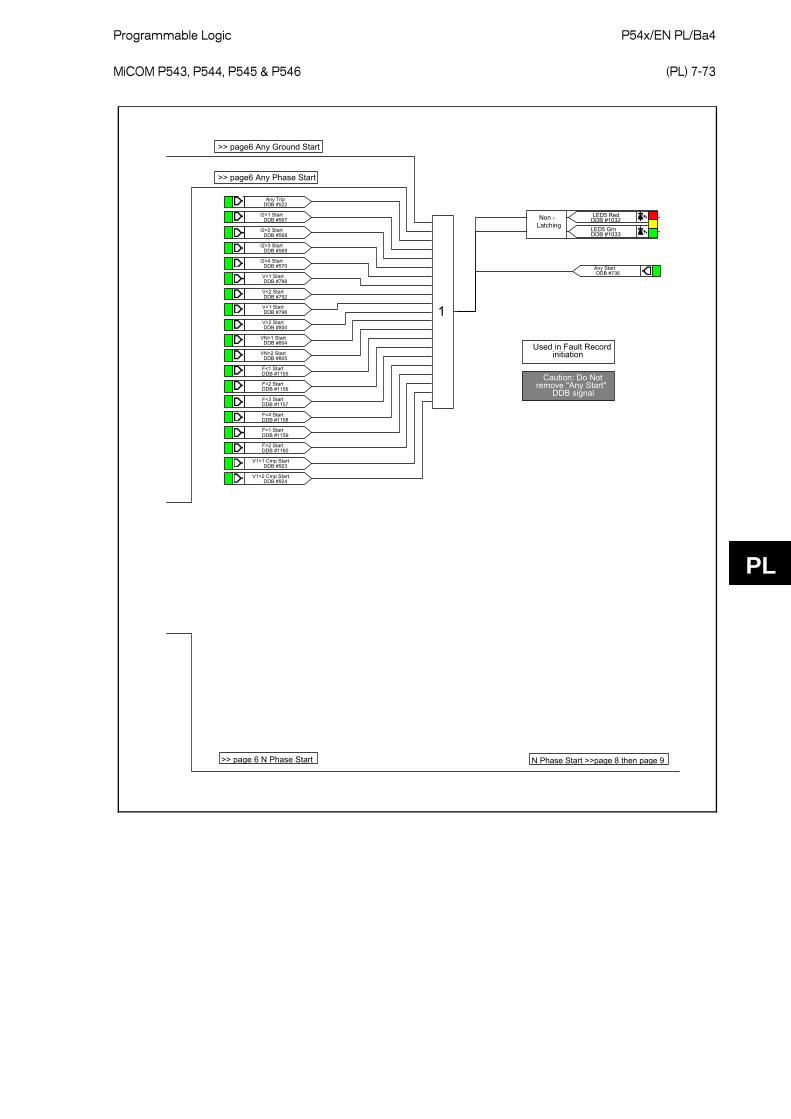
Programmable Logic P54x/EN PL/Ba4 MiCOM P543, P544, P545 & P546
(PL) 7-73
PL
DDB #788V<1 Start
DDB #792V<2 Start
DDB #796V>1 Start
DDB #800V>2 Start
DDB #804VN>1 Start
DDB #805VN>2 Start
DDB #736Any Start
1
Used in Fault Record initiation
Caution: Do Not remove "Any Start"
DDB signal
>> page6 Any Phase Start
DDB #1032Non -Latching
LED5 Red
DDB #1033LED5 Grn
>> page6 Any Ground Start
DDB #522Any Trip
DDB #567I2>1 Start
DDB #568I2>2 Start
DDB #569I2>3 Start
DDB #570I2>4 Start
DDB #1155F<1 Start
DDB #1156F<2 Start
DDB #1157F<3 Start
DDB #1158F<4 Start
DDB #1159F>1 Start
DDB #1160F>2 Start
>> page 6 N Phase Start
DDB #923V1>1 Cmp Start
DDB #924V1>2 Cmp Start
N Phase Start >>page 8 then page 9

P54x/EN PL/Ba4 Programmable Logic
(PL) 7-74
MiCOM P543, P544, P545 & P546
PL
DDB #609Zone 1 A Trip
1 DDB #952Faulted Phase A
DDB #614Zone 2 A Trip
DDB #619Zone 3 A Trip
DDB #624Zone P A Trip
DDB #629Zone 4 A Trip
DDB #633Aided 1 Trip A
DDB #643Aided 2 Trip A
DDB #647Aid 2 WI Trip A
DDB #637Aid 1 WI Trip A
DDB #656I>1 Trip A
DDB #660I>2 Trip A
DDB #664I>3 Trip A
DDB #668I>4 Trip A
DDB #577AR Trip Test A
DDB #610Zone 1 B Trip
DDB #615Zone 2 B Trip
DDB #620Zone 3 B Trip
DDB #630Zone 4 B Trip
DDB #625Zone P B Trip
DDB #634Aided 1 Trip B
DDB #644Aided 2 Trip B
DDB #638Aid 1 WI Trip B
DDB #648Aid 2 WI Trip B
DDB #657I>1 Trip B
DDB #661I>2 Trip B
DDB #665I>3 Trip B
DDB #669I>4 Trip B
DDB #578AR Trip Test B
1 DDB #953Faulted Phase B
DDB #583Diff Trip A
DDB #588Diff InterTrip B
DDB #584Diff Trip B
DDB #587Diff InterTrip A
Faulted Phase Flag, Used in Fault record and on LCD display.
Caution: Do Not remove "Faulted Phase" DDB
signals
>> page 6 then page 7 N Phase Start N Phase Start >> page 9
DDB #576AR Trip Test
DDB #576AR Trip Test

Programmable Logic P54x/EN PL/Ba4 MiCOM P543, P544, P545 & P546
(PL) 7-75
PL 1 DDB #955
Faulted Phase N
DDB #612Zone 1 N Trip
DDB #617Zone 2 N Trip
DDB #622Zone 3 N Trip
DDB #627Zone P N Trip
DDB #632Zone 4 N Trip
DDB #636Aided 1 Trip N
DDB #646Aided 2 Trip N
DDB #671IN>1 Trip
DDB #672IN>2 Trip
DDB #673IN>3 Trip
DDB #674IN>4 Trip
DDB #700VN>1 Trip
DDB #701VN>2 Trip
DDB #611Zone 1 C Trip
DDB #621Zone 3 C Trip
DDB #626Zone P C Trip
DDB #631Zone 4 C Trip
DDB #635Aided 1 Trip C
DDB #639Aid 1 WI Trip C
DDB #645Aided 2 Trip C
DDB #649Aid 2 WI Trip C
DDB #658I>1 Trip C
DDB #662I>2 Trip C
DDB #666I>3 Trip C
DDB #670I>4 Trip C
DDB #579AR Trip Test C
1 DDB #954Faulted Phase C
DDB #675ISEF>1 Trip
DDB #676ISEF>2 Trip
DDB #677ISEF>3 Trip
DDB #678ISEF>4 Trip
DDB #589Diff InterTrip C
DDB #585Diff Trip C
DDB #616Zone 2 C Trip
Faulted Phase Flag, Used in Fault record and on LCD display.
Caution: Do Not remove "Faulted Phase" DDB
signals
>> page 6 then page 7 the page 8 N Phase Start
DDB #576AR Trip Test
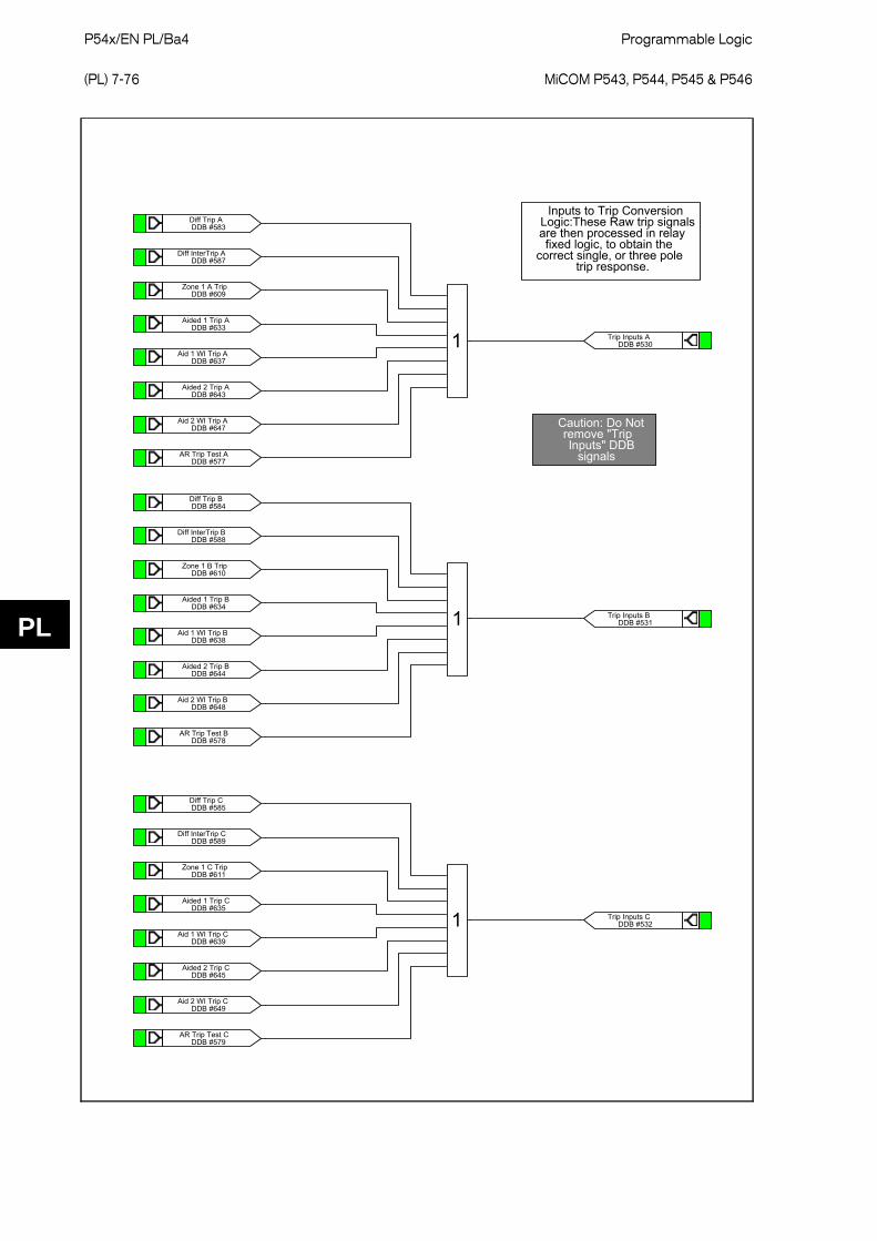
P54x/EN PL/Ba4 Programmable Logic
(PL) 7-76
MiCOM P543, P544, P545 & P546
PL
DDB #609Zone 1 A Trip
DDB #633Aided 1 Trip A
DDB #637Aid 1 WI Trip A
DDB #643Aided 2 Trip A
DDB #647Aid 2 WI Trip A
DDB #577AR Trip Test A
1 DDB #530Trip Inputs A
DDB #610Zone 1 B Trip
DDB #634Aided 1 Trip B
DDB #638Aid 1 WI Trip B
DDB #644Aided 2 Trip B
DDB #648Aid 2 WI Trip B
DDB #578AR Trip Test B
1 DDB #531Trip Inputs B
DDB #611Zone 1 C Trip
DDB #635Aided 1 Trip C
DDB #639Aid 1 WI Trip C
DDB #645Aided 2 Trip C
DDB #649Aid 2 WI Trip C
DDB #579AR Trip Test C
1 DDB #532Trip Inputs C
DDB #583Diff Trip A
DDB #587Diff InterTrip A
DDB #585Diff Trip C
DDB #589Diff InterTrip C
Inputs to Trip Conversion Logic:These Raw trip signals are then processed in relay fixed logic, to obtain the
correct single, or three pole trip response.
Caution: Do Not remove "Trip Inputs" DDB
signals
DDB #588Diff InterTrip B
DDB #584Diff Trip B
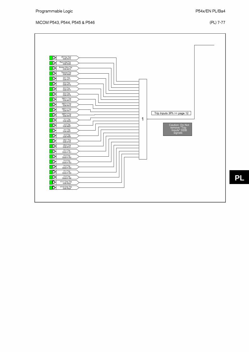
Programmable Logic P54x/EN PL/Ba4 MiCOM P543, P544, P545 & P546
(PL) 7-77
PL
DDB #576AR Trip Test
DDB #679Broken Wire Trip
DDB #680Thermal Trip
DDB #700VN>1 Trip
DDB #701VN>2 Trip
DDB #683V<1 Trip
DDB #687V<2 Trip
DDB #691V>1 Trip
DDB #695V>2 Trip
DDB #590Perm InterTrip
DDB #675ISEF>1 Trip
DDB #676ISEF>2 Trip
DDB #677ISEF>3 Trip
DDB #678ISEF>4 Trip
DDB #571I2>1 Trip
DDB #572I2>2 Trip
DDB #573I2>3 Trip
DDB #574I2>4 Trip
DDB #1161F<1 Trip
DDB #1162F<2 Trip
DDB #1163F<3 Trip
DDB #1164F<4 Trip
DDB #1165F>1 Trip
DDB #1166F>2 Trip
1Caution: Do Not remove "Trip Inputs" DDB
signals
Trip Inputs 3Ph >> page 12
DDB #925V1>1 Cmp Trip
DDB #926V1>2 Cmp Trip

P54x/EN PL/Ba4 Programmable Logic
(PL) 7-78
MiCOM P543, P544, P545 & P546
PL
DDB #613Zone 2 Trip
DDB #618Zone 3 Trip
DDB #623Zone P Trip
DDB #628Zone 4 Trip
DDB #655I>1 Trip
DDB #659I>2 Trip
DDB #663I>3 Trip
DDB #667I>4 Trip
DDB #671IN>1 Trip
DDB #672IN>2 Trip
DDB #673IN>3 Trip
DDB #674IN>4 Trip
DDB #641Aid1 DEF Trip3Ph
DDB #642Aid1 WI Trip 3Ph
DDB #651Aid2 DEF Trip3Ph
DDB #652Aid2 WI Trip 3Ph
DDB #654Loss ofLoad Trip
DDB #699Pole Discrepancy
DDB #704TOR Trip Zone 1
DDB #705TOR Trip Zone 2
DDB #706TOR Trip Zone 3
DDB #708TOR Trip Zone P
DDB #707TOR Trip Zone 4
DDB #709SOTF Trip Zone 1
DDB #710SOTF Trip Zone 2
DDB #711SOTF Trip Zone 3
DDB #713SOTF Trip Zone P
DDB #529Trip Inputs 3Ph
DDB #712SOTF Trip Zone 4
DDB #591Stub Bus Trip
Caution: Do Not remove "Trip Inputs" DDB
signals
DDB #553OST
DDB #551Pred. OST
DDB #557TOR Trip CNV
DDB #558SOTF Trip CNV
1
page 11 >> Trip Inputs 3Ph
DDB #640Aid1 Delta Tr3Ph
DDB #650Aid2 Delta Tr3Ph
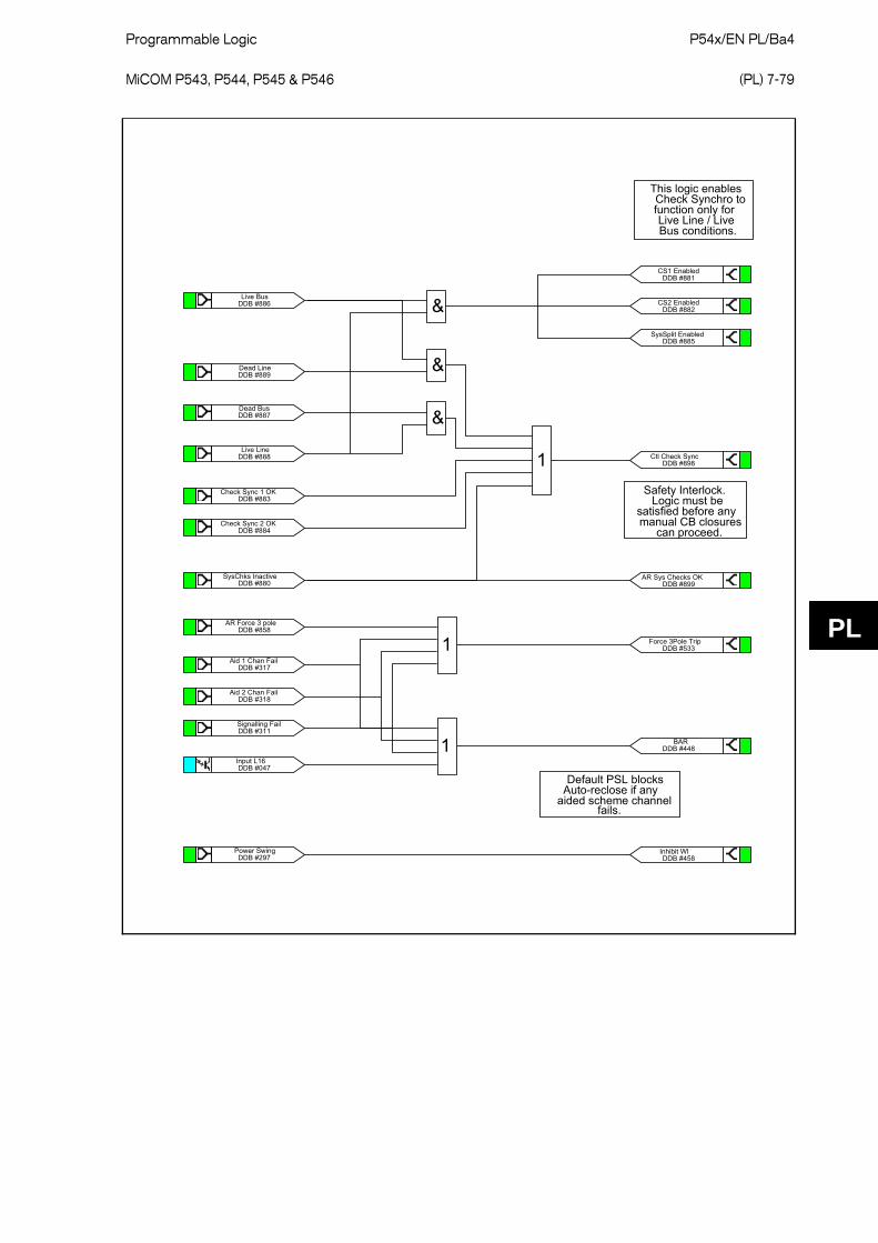
Programmable Logic P54x/EN PL/Ba4 MiCOM P543, P544, P545 & P546
(PL) 7-79
PL
DDB #886Live Bus
&
&
&
1
1
1
DDB #889Dead Line
DDB #887Dead Bus
DDB #888Live Line
DDB #881CS1 Enabled
DDB #882CS2 Enabled
DDB #885SysSplit Enabled
This logic enables Check Synchro to function only for Live Line / Live Bus conditions.
DDB #883Check Sync 1 OK
DDB #884Check Sync 2 OK
DDB #880SysChks Inactive
DDB #898Ctl Check Sync
DDB #899AR Sys Checks OK
Safety Interlock. Logic must be
satisfied before any manual CB closures
can proceed.
DDB #317Aid 1 Chan Fail
DDB #318Aid 2 Chan Fail
DDB #047Input L16
DDB #297Power Swing
DDB #533Force 3Pole Trip
DDB #858AR Force 3 pole
DDB #448BAR
Default PSL blocks Auto-reclose if any
aided scheme channel fails.
DDB #458Inhibit WI
DDB #311Signalling Fail

P54x/EN PL/Ba4 Programmable Logic
(PL) 7-80
MiCOM P543, P544, P545 & P546
PL
MiCOM P543 WITHOUT DISTANCE PROGRAMMABLE SCHEME LOGIC
Output Input Mappings
DDB #032Input L1
DDB #033Input L2
DDB #037Input L6
DDB #038Input L7
DDB #039Input L8
DDB #040Input L9
DDB #041Input L10
DDB #042Input L11
DDB #043Input L12
DDB #044Input L13
DDB #045Input L14
DDB #046Input L15
DDB #455Inhibit C Diff
DDB #456Recon Interlock
DDB #535External Trip A
DDB #536External Trip B
DDB #537External Trip C
DDB #425CB Aux A(52-B)
DDB #426CB Aux B(52-B)
DDB #427CB Aux C(52-B)
DDB #438MCB/VTS
DDB #440Init Close CB
DDB #446Reset Lockout
DDB #436CB Healthy
External Trips: Initiate Breaker
Fail, and Auto-reclose (if enabled).
DDB #047Input L16
DDB #448BAR
Opto L5 can be found on other pages

Programmable Logic P54x/EN PL/Ba4 MiCOM P543, P544, P545 & P546
(PL) 7-81
PL
Output Contacts
DDB #523Trip Output A
DDB #524Trip Output B
DDB #525Trip Output C
Dwell
100
0
Output R9DDB #008
Dwell
100
0
Output R10DDB #009
Dwell
100
0
Output R11DDB #010
Straight
0
0
Output R2DDB #001
Dwell
100
0
Output R3DDB #002
Straight
0
0
Output R5DDB #004
Dwell
100
0
Output R6DDB #005
Straight
0
0
Output R7DDB #006
Straight
0
0
Output R8DDB #007
DDB #311Signalling Fail
DDB #522Any Trip
DDB #096IM64 Ch1 Input 1
DDB #104IM64 Ch2 Input 1 1
DDB #834Bfail1 Trip 3ph
DDB #839Control Close
DDB #838Control Trip
Trip Outputs are generated by the
internal single/three phase
trip conversion logic.
Straight
0
0
Output R12DDB #0111DDB #844
AR 3pole in prog
DDB #845AR 1pole in prog
Straight
0
0
Output R13DDB #012DDB #852
Successful Close
Straight
0
0
Output R14DDB #013DDB #306
A/R Lockout
Straight
0
0
Output R1DDB #000
DDB #582Diff Trip
DDB #586Diff InterTrip 1

P54x/EN PL/Ba4 Programmable Logic
(PL) 7-82
MiCOM P543, P544, P545 & P546
PL
Output Contacts

Programmable Logic P54x/EN PL/Ba4 MiCOM P543, P544, P545 & P546
(PL) 7-83
PL
LEDs
DDB #522Any Trip
DDB #702Fault REC TRIG
DDB #582Diff Trip
DDB #291Test Loopback
DDB #306A/R Lockout
DDB #844AR 3pole in prog
DDB #845AR 1pole in prog
DDB #311Signalling Fail
DDB #1024LatchingLED1 Red
DDB #1025LED1 Grn
DDB #1030Non -Latching
LED4 Red
DDB #1031LED4 Grn
DDB #1034Non -Latching
LED6 Red
DDB #1035LED6 Grn
DDB #1036Non -Latching
LED7 Red
DDB #1037LED7 Grn
DDB #1038Non -Latching
LED8 Red
DDB #1039LED8 Grn
1DDB #586
Diff InterTrip
1
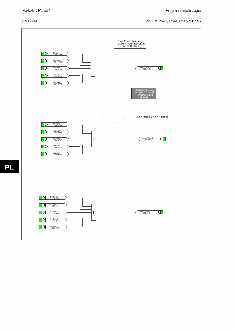
P54x/EN PL/Ba4 Programmable Logic
(PL) 7-84
MiCOM P543, P544, P545 & P546
PL
DDB #762I>1 Start A
DDB #766I>2 Start A 1
DDB #770I>3 Start A
DDB #774I>4 Start A
DDB #763I>1 Start B
DDB #767I>2 Start B
DDB #771I>3 Start B
DDB #775I>4 Start B
1
DDB #764I>1 Start C
DDB #768I>2 Start C
DDB #772I>3 Start C
DDB #776I>4 Start C
1
DDB #956Started Phase A
1Any Phase Start >> page6
DDB #957Started Phase B
DDB #958Started Phase C
DDB #738Diff Start A
DDB #739Diff Start B
DDB #740Diff Start C
Any Phase Start >> page6Any Phase Start >> page6
Start Phase Mappings. Used in Fault Record &
on LCD Display
Caution: Do Not remove "Started
Phase" DDB signals

Programmable Logic P54x/EN PL/Ba4 MiCOM P543, P544, P545 & P546
(PL) 7-85
PL

P54x/EN PL/Ba4 Programmable Logic
(PL) 7-86
MiCOM P543, P544, P545 & P546
PL

Programmable Logic P54x/EN PL/Ba4 MiCOM P543, P544, P545 & P546
(PL) 7-87
PL

P54x/EN PL/Ba4 Programmable Logic
(PL) 7-88
MiCOM P543, P544, P545 & P546
PL
1 DDB #955Faulted Phase N
DDB #671IN>1 Trip
DDB #672IN>2 Trip
DDB #673IN>3 Trip
DDB #674IN>4 Trip
DDB #700VN>1 Trip
DDB #701VN>2 Trip
DDB #658I>1 Trip C
DDB #662I>2 Trip C
DDB #666I>3 Trip C
DDB #670I>4 Trip C
DDB #579AR Trip Test C
1 DDB #954Faulted Phase C
DDB #675ISEF>1 Trip
DDB #676ISEF>2 Trip
DDB #677ISEF>3 Trip
DDB #678ISEF>4 Trip
Faulted Phase Flag, Used in Fault record and on LCD display.
Caution: Do Not remove "Faulted Phase" DDB
signals
DDB #589Diff InterTrip C
DDB #585Diff Trip C
DDB #576AR Trip Test

Programmable Logic P54x/EN PL/Ba4 MiCOM P543, P544, P545 & P546
(PL) 7-89
PL
DDB #577AR Trip Test A
1 DDB #530Trip Inputs A
DDB #578AR Trip Test B
1 DDB #531Trip Inputs B
DDB #579AR Trip Test C
1 DDB #532Trip Inputs C
DDB #583Diff Trip A
DDB #587Diff InterTrip A
DDB #585Diff Trip C
DDB #589Diff InterTrip C
Inputs to Trip Conversion Logic:These Raw trip signals are then processed in relay fixed logic, to obtain the
correct single, or three pole trip response.
Caution: Do Not remove "Trip Inputs" DDB
signals
DDB #588Diff InterTrip B
DDB #584Diff Trip B

P54x/EN PL/Ba4 Programmable Logic
(PL) 7-90
MiCOM P543, P544, P545 & P546
PL

Programmable Logic P54x/EN PL/Ba4 MiCOM P543, P544, P545 & P546
(PL) 7-91
PL
DDB #886Live Bus
&
&
&
1
DDB #889Dead Line
DDB #887Dead Bus
DDB #888Live Line
DDB #881CS1 Enabled
DDB #882CS2 Enabled
DDB #885SysSplit Enabled
This logic enables Check Synchro to function only for Live Line / Live Bus conditions.
DDB #883Check Sync 1 OK
DDB #884Check Sync 2 OK
DDB #880SysChks Inactive
DDB #898Ctl Check Sync
DDB #899AR Sys Checks OK
Safety Interlock. Logic must be
satisfied before any manual CB closures
can proceed.
DDB #533Force 3Pole Trip
DDB #858AR Force 3 pole

P54x/EN PL/Ba4 Programmable Logic
(PL) 7-92
MiCOM P543, P544, P545 & P546
PL
MiCOM P544 WITH DISTANCE PROGRAMMABLE SCHEME LOGIC Output Input Mappings

Programmable Logic P54x/EN PL/Ba4 MiCOM P543, P544, P545 & P546
(PL) 7-93
PL
Output Contacts
DDB #523CB1 Trip OutputA
DDB #524CB1 Trip OutputB
DDB #525CB1 Trip OutputC
Dwell
100
0
Output R9DDB #008
Dwell
100
0
Output R10DDB #009
Dwell100
0
Output R11DDB #010
Straight
0
0
Output R1DDB #000
Straight
0
0
Output R2DDB #001
Dwell100
0
Output R3DDB #002
Straight
0
0
Output R5DDB #004
Dwell
100
0
Output R6DDB #005
Straight
0
0
Output R7DDB #006
Straight
0
0
Output R8DDB #007
DDB #608Zone 1 Trip
DDB #311Signalling Fail
DDB #522Any Trip
DDB #096IM64 Ch1 Input 1
DDB #104IM64 Ch2 Input 1 1
DDB #834CB1 Fail1 Trip
DDB #839Control CloseCB1
DDB #838Control TripCB1
Dwell
100
0
Output R12DDB #011
Straight
0
0
Output R13DDB #012
Straight0
0
Output R14DDB #013
DDB #841Control CloseCB2
DDB #840Control TripCB2
DDB #582Diff Trip
DDB #586Diff InterTrip
1
DDB #836CB2 Fail1 Trip
Trip Outputs are
generated by the internal single/three phase trip conversion
logic.
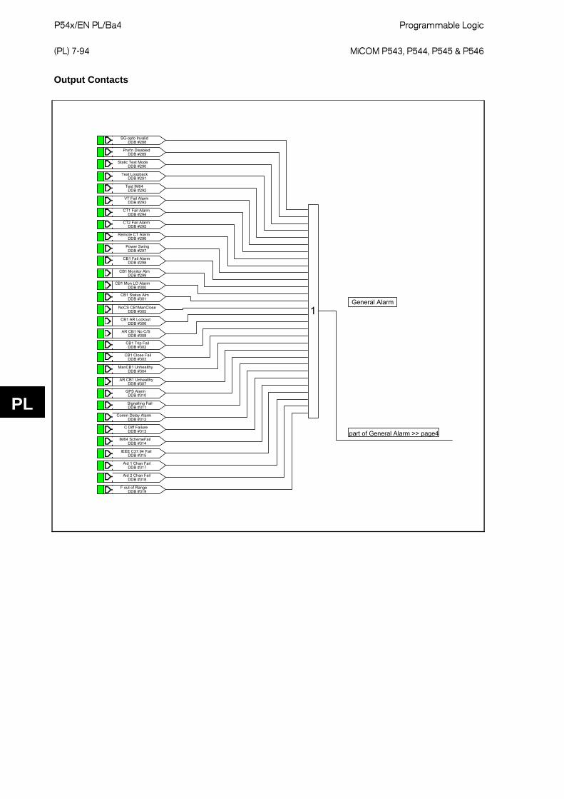
P54x/EN PL/Ba4 Programmable Logic
(PL) 7-94
MiCOM P543, P544, P545 & P546
PL
Output Contacts
DDB #288SG-opto Invalid
DDB #289Prot'n Disabled
DDB #293VT Fail Alarm
DDB #294CT1 Fail Alarm
DDB #297Power Swing
DDB #298CB1 Fail Alarm
DDB #301CB1 Status Alm
DDB #290Static Test Mode
DDB #291Test Loopback
DDB #292Test IM64
DDB #302CB1 Trip Fail
DDB #303CB1 Close Fail
DDB #304ManCB1 Unhealthy
DDB #310GPS Alarm
DDB #311Signalling Fail
DDB #312Comm Delay Alarm
DDB #313C Diff Failure
DDB #314IM64 SchemeFail
DDB #315IEEE C37.94 Fail
DDB #317Aid 1 Chan Fail
DDB #318Aid 2 Chan Fail
DDB #319F out of Range
1
DDB #295CT2 Fail Alarm
DDB #296Remote CT Alarm
General Alarm
DDB #299CB1 Monitor Alm
DDB #300CB1 Mon LO Alarm
DDB #305NoCS CB1ManClose
DDB #306CB1 AR Lockout
DDB #308AR CB1 No C/S
part of General Alarm >> page4
DDB #307AR CB1 Unhealthy
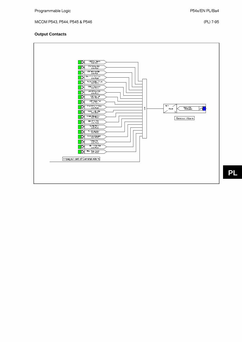
Programmable Logic P54x/EN PL/Ba4 MiCOM P543, P544, P545 & P546
(PL) 7-95
PL
Output Contacts

P54x/EN PL/Ba4 Programmable Logic
(PL) 7-96
MiCOM P543, P544, P545 & P546
PL
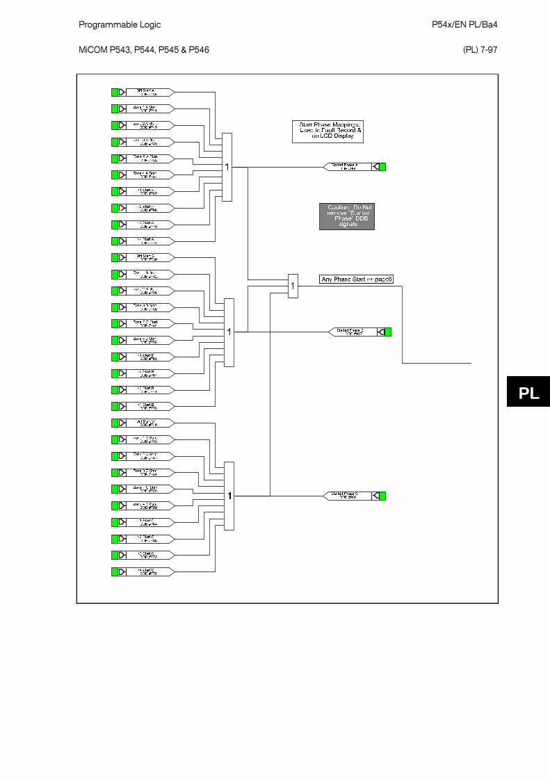
Programmable Logic P54x/EN PL/Ba4 MiCOM P543, P544, P545 & P546
(PL) 7-97
PL

P54x/EN PL/Ba4 Programmable Logic
(PL) 7-98
MiCOM P543, P544, P545 & P546
PL
DDB #744Zone 1 N Start
DDB #748Zone 2 N Start
DDB #752Zone 3 N Start
DDB #760Zone 4 N Start
DDB #777IN>1 Start
DDB #778IN>2 Start
DDB #779IN>3 Start
DDB #780IN>4 Start
1
Any Ground Start >> page 7
DDB #1013Phase Select N
DDB #522Any Trip
&
DDB #036Input L5
DDB #1013Phase Select N
DDB #522Any Trip
Pulse10
0
&
1
DDB #959Started Phase N
DDB #444Reset Relays/LED
DDB #781ISEF>1 Start
DDB #782ISEF>2 Start
DDB #783ISEF>3 Start
DDB #784ISEF>4 Start
Any Ground Start >> page 7Any Ground Start >> page 7
Any Phase Start >> page 7
DDB #756Zone P N Start
>> page5 Any Phase Start
N Phase Start >> page 7 then page 8 then page 9
This logic ensures correct N indications for faults involving ground. The pulse prevents pole
scatter affecting the N indication.
This logic clears all latched indications at the start of Any Trip
This reset controls: Reset latched relays, Reset latched
LEDs.
&DDB #1385
AR In Service

Programmable Logic P54x/EN PL/Ba4 MiCOM P543, P544, P545 & P546
(PL) 7-99
PL

P54x/EN PL/Ba4 Programmable Logic
(PL) 7-100
MiCOM P543, P544, P545 & P546
PL
DDB #609Zone 1 A Trip
1 DDB #952Faulted Phase A
DDB #614Zone 2 A Trip
DDB #619Zone 3 A Trip
DDB #624Zone P A Trip
DDB #629Zone 4 A Trip
DDB #633Aided 1 Trip A
DDB #643Aided 2 Trip A
DDB #647Aid 2 WI Trip A
DDB #637Aid 1 WI Trip A
DDB #656I>1 Trip A
DDB #660I>2 Trip A
DDB #664I>3 Trip A
DDB #668I>4 Trip A
DDB #610Zone 1 B Trip
DDB #615Zone 2 B Trip
DDB #620Zone 3 B Trip
DDB #630Zone 4 B Trip
DDB #625Zone P B Trip
DDB #634Aided 1 Trip B
DDB #644Aided 2 Trip B
DDB #638Aid 1 WI Trip B
DDB #648Aid 2 WI Trip B
DDB #657I>1 Trip B
DDB #661I>2 Trip B
DDB #665I>3 Trip B
DDB #669I>4 Trip B
1 DDB #953Faulted Phase B
DDB #583Diff Trip A
DDB #588Diff InterTrip B
DDB #584Diff Trip B
DDB #587Diff InterTrip A
>> page 6 then page 7 N Phase Start N Phase Start >> page 9
Faulted Phase Flag, Used in Fault record and on LCD display.
Caution: Do Not remove "Faulted
Phase" DDB signals
DDB #577AR Trip Test A
DDB #578AR Trip Test B

Programmable Logic P54x/EN PL/Ba4 MiCOM P543, P544, P545 & P546
(PL) 7-101
PL 1 DDB #955
Faulted Phase N
DDB #612Zone 1 N Trip
DDB #617Zone 2 N Trip
DDB #622Zone 3 N Trip
DDB #627Zone P N Trip
DDB #632Zone 4 N Trip
DDB #636Aided 1 Trip N
DDB #646Aided 2 Trip N
DDB #671IN>1 Trip
DDB #672IN>2 Trip
DDB #673IN>3 Trip
DDB #674IN>4 Trip
DDB #700VN>1 Trip
DDB #701VN>2 Trip
DDB #611Zone 1 C Trip
DDB #621Zone 3 C Trip
DDB #626Zone P C Trip
DDB #631Zone 4 C Trip
DDB #635Aided 1 Trip C
DDB #639Aid 1 WI Trip C
DDB #645Aided 2 Trip C
DDB #649Aid 2 WI Trip C
DDB #658I>1 Trip C
DDB #662I>2 Trip C
DDB #666I>3 Trip C
DDB #670I>4 Trip C
1 DDB #954Faulted Phase C
DDB #675ISEF>1 Trip
DDB #676ISEF>2 Trip
DDB #677ISEF>3 Trip
DDB #678ISEF>4 Trip
DDB #589Diff InterTrip C
DDB #585Diff Trip C
DDB #616Zone 2 C Trip
>> page 6 then page 7 then page 8 N Phase Start
Faulted Phase Flag, Used in Fault record and on LCD display.
Caution: Do Not remove "Faulted
Phase" DDB signals
DDB #579AR Trip Test C

P54x/EN PL/Ba4 Programmable Logic
(PL) 7-102
MiCOM P543, P544, P545 & P546
PL
DDB #609Zone 1 A Trip
DDB #633Aided 1 Trip A
DDB #637Aid 1 WI Trip A
DDB #643Aided 2 Trip A
DDB #647Aid 2 WI Trip A
1 DDB #530Trip Inputs A
DDB #610Zone 1 B Trip
DDB #634Aided 1 Trip B
DDB #638Aid 1 WI Trip B
DDB #644Aided 2 Trip B
DDB #648Aid 2 WI Trip B
1 DDB #531Trip Inputs B
DDB #611Zone 1 C Trip
DDB #635Aided 1 Trip C
DDB #639Aid 1 WI Trip C
DDB #645Aided 2 Trip C
DDB #649Aid 2 WI Trip C
1 DDB #532Trip Inputs C
DDB #583Diff Trip A
DDB #587Diff InterTrip A
DDB #585Diff Trip C
DDB #589Diff InterTrip C
DDB #584Diff Trip B
DDB #588Diff InterTrip B
Inputs to Trip Conversion Logic:These Raw trip signals are then processed in relay fixed logic, to obtain the
correct single, or three pole trip response.
Caution: Do Not remove "Trip Inputs" DDB
signalsDDB #577
AR Trip Test A
DDB #578AR Trip Test B
DDB #579AR Trip Test C

Programmable Logic P54x/EN PL/Ba4 MiCOM P543, P544, P545 & P546
(PL) 7-103
PL
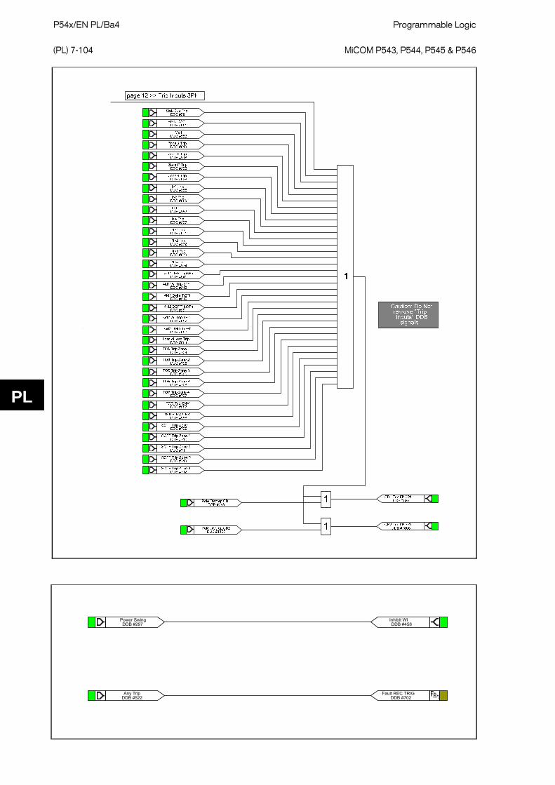
P54x/EN PL/Ba4 Programmable Logic
(PL) 7-104
MiCOM P543, P544, P545 & P546
PL
DDB #522Any Trip
DDB #702Fault REC TRIG
DDB #297Power Swing
DDB #458Inhibit WI
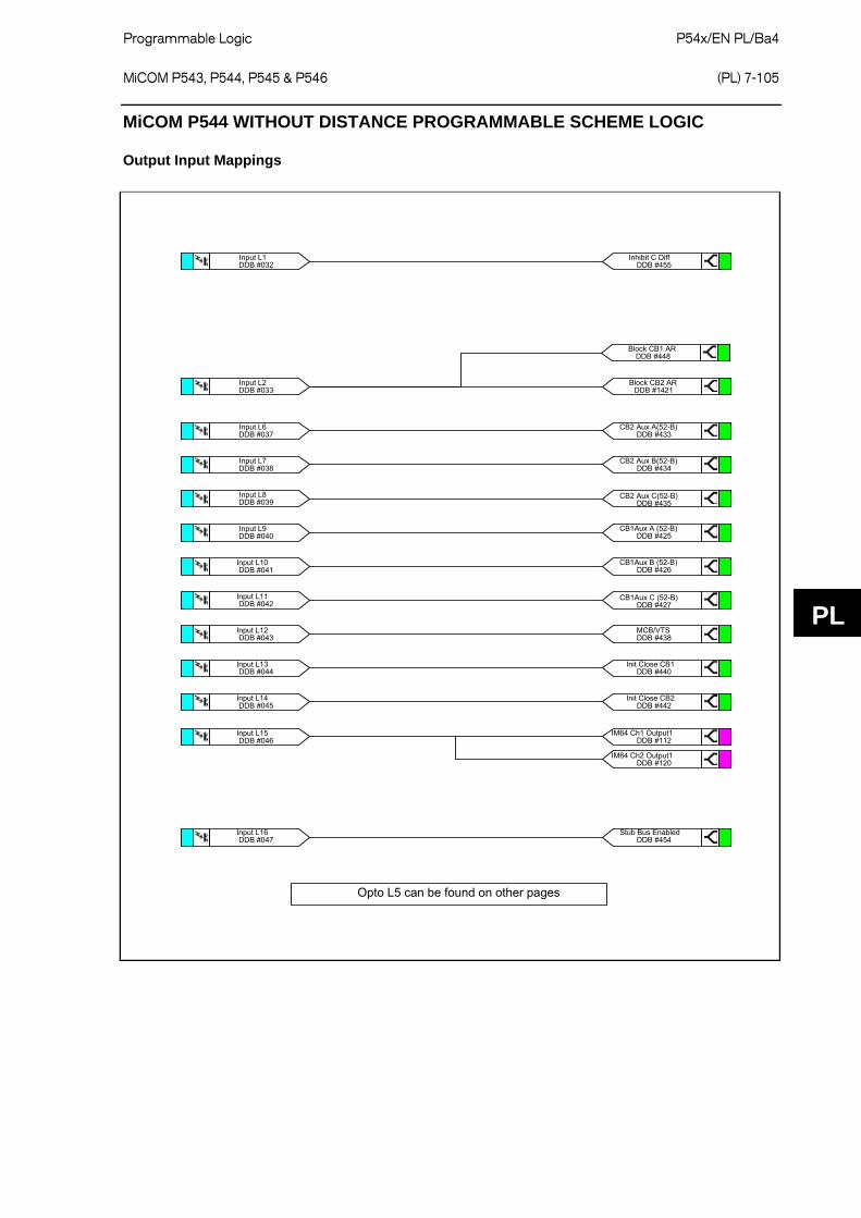
Programmable Logic P54x/EN PL/Ba4 MiCOM P543, P544, P545 & P546
(PL) 7-105
PL
MiCOM P544 WITHOUT DISTANCE PROGRAMMABLE SCHEME LOGIC
Output Input Mappings
DDB #032Input L1
DDB #037Input L6
DDB #038Input L7
DDB #039Input L8
DDB #040Input L9
DDB #041Input L10
DDB #042Input L11
DDB #043Input L12
DDB #044Input L13
DDB #045Input L14
DDB #455Inhibit C Diff
DDB #425CB1Aux A (52-B)
DDB #426CB1Aux B (52-B)
DDB #427CB1Aux C (52-B)
DDB #438MCB/VTS
DDB #440Init Close CB1
DDB #433CB2 Aux A(52-B)
DDB #434CB2 Aux B(52-B)
DDB #435CB2 Aux C(52-B)
DDB #047Input L16
DDB #454Stub Bus Enabled
DDB #442Init Close CB2
Opto L5 can be found on other pages
DDB #046Input L15
DDB #112IM64 Ch1 Output1
DDB #120IM64 Ch2 Output1
DDB #033Input L2
DDB #1421Block CB2 AR
DDB #448Block CB1 AR

P54x/EN PL/Ba4 Programmable Logic
(PL) 7-106
MiCOM P543, P544, P545 & P546
PL
Output Contacts
DDB #523CB1 Trip OutputA
DDB #524CB1 Trip OutputB
DDB #525CB1 Trip OutputC
Dwell
100
0
Output R9DDB #008
Dwell100
0
Output R10DDB #009
Dwell
100
0
Output R11DDB #010
Straight
0
0
Output R1DDB #000
Straight0
0
Output R2DDB #001
Dwell
100
0
Output R3DDB #002
Straight
0
0
Output R5DDB #004
Dwell
100
0
Output R6DDB #005
Straight
0
0
Output R7DDB #006
Straight0
0
Output R8DDB #007
DDB #311Signalling Fail
DDB #522Any Trip
DDB #096IM64 Ch1 Input 1
DDB #104IM64 Ch2 Input 1 1
DDB #834CB1 Fail1 Trip
DDB #839Control CloseCB1
DDB #838Control TripCB1
Dwell100
0
Output R12DDB #011
Straight
0
0
Output R13DDB #012
Straight0
0
Output R14DDB #013
DDB #841Control CloseCB2
DDB #840Control TripCB2
DDB #582Diff Trip
DDB #586Diff InterTrip 1
DDB #836CB2 Fail1 Trip
Trip Outputs are
generated by the internal single/three phase trip conversion
logic.

Programmable Logic P54x/EN PL/Ba4 MiCOM P543, P544, P545 & P546
(PL) 7-107
PL
Output Contacts

P54x/EN PL/Ba4 Programmable Logic
(PL) 7-108
MiCOM P543, P544, P545 & P546
PL
Output Contacts

Programmable Logic P54x/EN PL/Ba4 MiCOM P543, P544, P545 & P546
(PL) 7-109
PL
LEDs
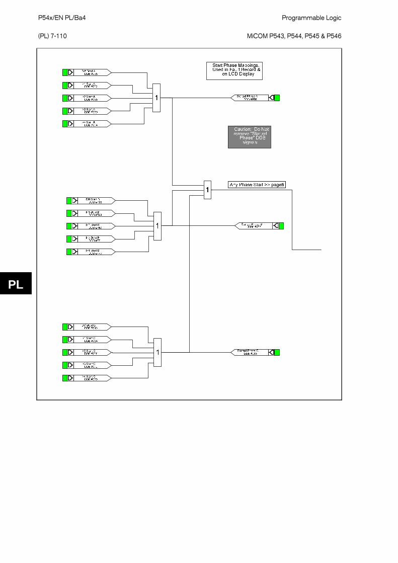
P54x/EN PL/Ba4 Programmable Logic
(PL) 7-110
MiCOM P543, P544, P545 & P546
PL

Programmable Logic P54x/EN PL/Ba4 MiCOM P543, P544, P545 & P546
(PL) 7-111
PL

P54x/EN PL/Ba4 Programmable Logic
(PL) 7-112
MiCOM P543, P544, P545 & P546
PL
DDB #788V<1 Start
DDB #792V<2 Start
DDB #796V>1 Start
DDB #800V>2 Start
DDB #804VN>1 Start
DDB #805VN>2 Start
DDB #736Any Start1
DDB #1032Non -Latching
LED5 Red
DDB #1033LED5 Grn
>> page 6 Any Ground Start
DDB #522Any Trip
>> page 6 Any Phase Start
DDB #567I2>1 Start
DDB #568I2>2 Start
DDB #569I2>3 Start
DDB #570I2>4 Start
DDB #1155F<1 Start
DDB #1156F<2 Start
DDB #1157F<3 Start
DDB #1158F<4 Start
DDB #1159F>1 Start
DDB #1160F>2 Start
Used in Fault Record initiation
Caution: Do Not remove "Any Start" DDB
signal
DDB #923V1>1 Cmp Start
DDB #924V1>2 Cmp Start
DDB #597df/dt>1 Start
DDB #598df/dt>2 Start
DDB #599df/dt>3 Start
DDB #600df/dt>4 Start

Programmable Logic P54x/EN PL/Ba4 MiCOM P543, P544, P545 & P546
(PL) 7-113
PL

P54x/EN PL/Ba4 Programmable Logic
(PL) 7-114
MiCOM P543, P544, P545 & P546
PL 1 DDB #955
Faulted Phase N
DDB #671IN>1 Trip
DDB #672IN>2 Trip
DDB #673IN>3 Trip
DDB #674IN>4 Trip
DDB #700VN>1 Trip
DDB #701VN>2 Trip
DDB #658I>1 Trip C
DDB #662I>2 Trip C
DDB #666I>3 Trip C
DDB #670I>4 Trip C
1 DDB #954Faulted Phase C
DDB #675ISEF>1 Trip
DDB #676ISEF>2 Trip
DDB #677ISEF>3 Trip
DDB #678ISEF>4 Trip
DDB #589Diff InterTrip C
DDB #585Diff Trip C
Faulted Phase Flag, Used in Fault record and on LCD display.
Caution: Do Not remove "Faulted
Phase" DDB signals
DDB #579AR Trip Test C

Programmable Logic P54x/EN PL/Ba4 MiCOM P543, P544, P545 & P546
(PL) 7-115
PL
1 DDB #530Trip Inputs A
1 DDB #531Trip Inputs B
1 DDB #532Trip Inputs C
DDB #583Diff Trip A
DDB #587Diff InterTrip A
DDB #585Diff Trip C
DDB #589Diff InterTrip C
DDB #584Diff Trip B
DDB #588Diff InterTrip B
Inputs to Trip Conversion Logic:These Raw trip signals are then processed in relay fixed logic, to obtain the
correct single, or three pole trip response.
Caution: Do Not remove "Trip Inputs" DDB
signals
DDB #577AR Trip Test A
DDB #578AR Trip Test B
DDB #579AR Trip Test C

P54x/EN PL/Ba4 Programmable Logic
(PL) 7-116
MiCOM P543, P544, P545 & P546
PL
DDB #679Broken Wire Trip
DDB #680Thermal Trip
DDB #700VN>1 Trip
DDB #701VN>2 Trip
DDB #683V<1 Trip
DDB #687V<2 Trip
DDB #691V>1 Trip
DDB #695V>2 Trip
DDB #590Perm InterTrip
DDB #675ISEF>1 Trip
DDB #676ISEF>2 Trip
DDB #677ISEF>3 Trip
DDB #678ISEF>4 Trip
DDB #571I2>1 Trip
DDB #572I2>2 Trip
DDB #573I2>3 Trip
DDB #574I2>4 Trip
DDB #1161F<1 Trip
DDB #1162F<2 Trip
DDB #1163F<3 Trip
DDB #1164F<4 Trip
DDB #1165F>1 Trip
DDB #1166F>2 Trip
1
Trip Inputs 3Ph >> page 12
Caution: Do Not remove "Trip Inputs" DDB
signals
DDB #925V1>1 Cmp Trip
DDB #926V1>2 Cmp Trip
DDB #601df/dt>1 Trip
DDB #602df/dt>2 Trip
DDB #603df/dt>3 Trip
DDB #604df/dt>4 Trip
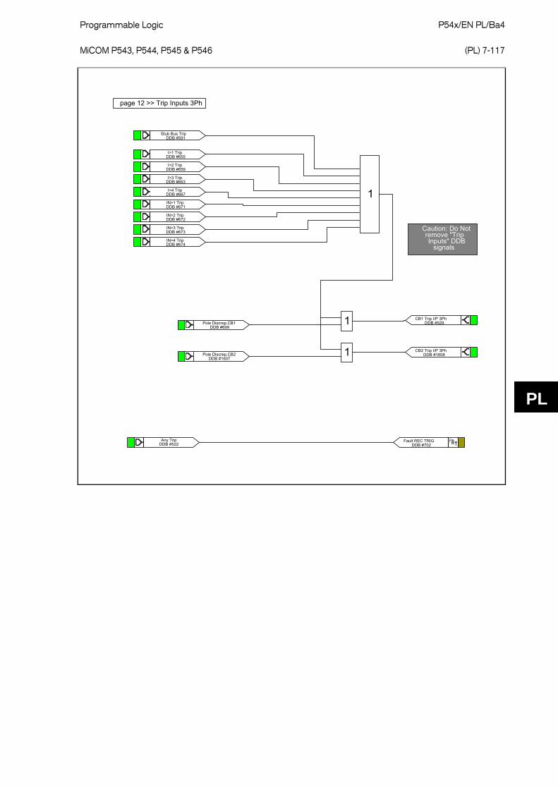
Programmable Logic P54x/EN PL/Ba4 MiCOM P543, P544, P545 & P546
(PL) 7-117
PL
DDB #522Any Trip
DDB #702Fault REC TRIG
DDB #655I>1 Trip
DDB #659I>2 Trip
DDB #663I>3 Trip
DDB #667I>4 Trip
DDB #671IN>1 Trip
DDB #672IN>2 Trip
DDB #673IN>3 Trip
DDB #674IN>4 Trip
DDB #529CB1 Trip I/P 3Ph
1
DDB #591Stub Bus Trip
page 12 >> Trip Inputs 3Ph
Caution: Do Not remove "Trip Inputs" DDB
signals
DDB #1608CB2 Trip I/P 3Ph
DDB #699Pole Discrep.CB1
DDB #1607Pole Discrep.CB2
1
1

P54x/EN PL/Ba4 Programmable Logic
(PL) 7-118
MiCOM P543, P544, P545 & P546
PL
MiCOM P545 WITH DISTANCE PROGRAMMABLE SCHEME LOGIC
Output Input Mappings

Programmable Logic P54x/EN PL/Ba4 MiCOM P543, P544, P545 & P546
(PL) 7-119
PL
Output Contacts

P54x/EN PL/Ba4 Programmable Logic
(PL) 7-120
MiCOM P543, P544, P545 & P546
PL
Output Contacts
DDB #288SG-opto Invalid
DDB #289Prot'n Disabled
DDB #293VT Fail Alarm
DDB #294CT Fail Alarm
DDB #297Power Swing
DDB #298CB Fail Alarm
DDB #299CB Monitor Alarm
DDB #300CB Lockout Alarm
DDB #301CB Status Alarm
DDB #290Static Test Mode
DDB #291Test Loopback
DDB #292Test IM64
DDB #302CB Trip Fail
DDB #303CB Close Fail
DDB #304Man CB Unhealthy
DDB #305No C/S Man Close
DDB #306A/R Lockout
DDB #307A/R CB Unhealthy
DDB #308A/R No Checksync
DDB #309System Split
DDB #310GPS Alarm
DDB #311Signalling Fail
DDB #312Comm Delay Alarm
DDB #313C Diff Failure
DDB #314IM64 SchemeFail
DDB #315IEEE C37.94 Fail
DDB #317Aid 1 Chan Fail
DDB #318Aid 2 Chan Fail
DDB #319F out of Range
DDB #332Incompatible Rly
DDB #333InValid Mesg Fmt
DDB #334Main Prot. Fail
DDB #335Config Error
DDB #336Re-Config Error
DDB #337Comms Changed
DDB #352Battery Fail
DDB #353Field Volts Fail
1 Dwell500
0
Output R4DDB #003
General Alarm
DDB #296Remote CT Alarm
Output Contacts
DDB #338Max Prop. Alarm
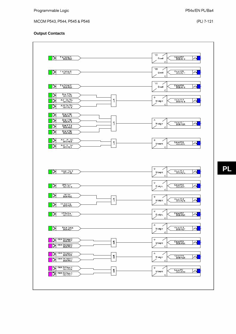
Programmable Logic P54x/EN PL/Ba4 MiCOM P543, P544, P545 & P546
(PL) 7-121
PL
Output Contacts

P54x/EN PL/Ba4 Programmable Logic
(PL) 7-122
MiCOM P543, P544, P545 & P546
PL
LEDs

Programmable Logic P54x/EN PL/Ba4 MiCOM P543, P544, P545 & P546
(PL) 7-123
PL
DDB #741Zone 1 A Start
DDB #745Zone 2 A Start
DDB #749Zone 3 A Start
DDB #753Zone P A Start
DDB #757Zone 4 A Start
DDB #762I>1 Start A
DDB #766I>2 Start A
1
DDB #770I>3 Start A
DDB #774I>4 Start A
DDB #742Zone 1 B Start
DDB #746Zone 2 B Start
DDB #750Zone 3 B Start
DDB #754Zone P B Start
DDB #758Zone 4 B Start
DDB #763I>1 Start B
DDB #767I>2 Start B
DDB #771I>3 Start B
DDB #775I>4 Start B
1
DDB #743Zone 1 C Start
DDB #747Zone 2 C Start
DDB #751Zone 3 C Start
DDB #755Zone P C Start
DDB #759Zone 4 C Start
DDB #764I>1 Start C
DDB #768I>2 Start C
DDB #772I>3 Start C
DDB #776I>4 Start C
1
DDB #956Started Phase A
1Any Phase Start >>page 7
DDB #957Started Phase B
DDB #958Started Phase C
DDB #738Diff Start A
DDB #739Diff Start B
DDB #740Diff Start C
Any Phase Start >>page 7Any Phase Start >>page 7
Start Phase Mappings. Used in Fault Record &
on LCD Display
Caution: Do Not remove "Started
Phase" DDB signals

P54x/EN PL/Ba4 Programmable Logic
(PL) 7-124
MiCOM P543, P544, P545 & P546
PL
DDB #744Zone 1 N Start
DDB #748Zone 2 N Start
DDB #752Zone 3 N Start
DDB #760Zone 4 N Start
DDB #777IN>1 Start
DDB #778IN>2 Start
DDB #779IN>3 Start
DDB #780IN>4 Start
1
DDB #1013Phase Select N
DDB #522Any Trip
&
DDB #036Input L5
DDB #856A/R Status 3P
DDB #857A/R Status 1P
DDB #1013Phase Select N
DDB #522Any Trip
Pulse
10
0
&
&
1
DDB #959Started Phase N
DDB #444Reset Relays/LED
DDB #781ISEF>1 Start
DDB #782ISEF>2 Start
DDB #783ISEF>3 Start
DDB #784ISEF>4 Start
This reset controls: Reset latched relays, Reset latched LEDs, Reset A/R
Lockout.This logic clears all latched indications at the start of Any Trip
This logic ensures correct N indications for faults involving ground. The pulse prevents pole
scatter affecting the N indication.
Any Phase Start >>page8
DDB #756Zone P N Start
>>page6 Any Phase Start
N Phase Start >> page8 then page 9 then page 10
Any Ground Start >> page8
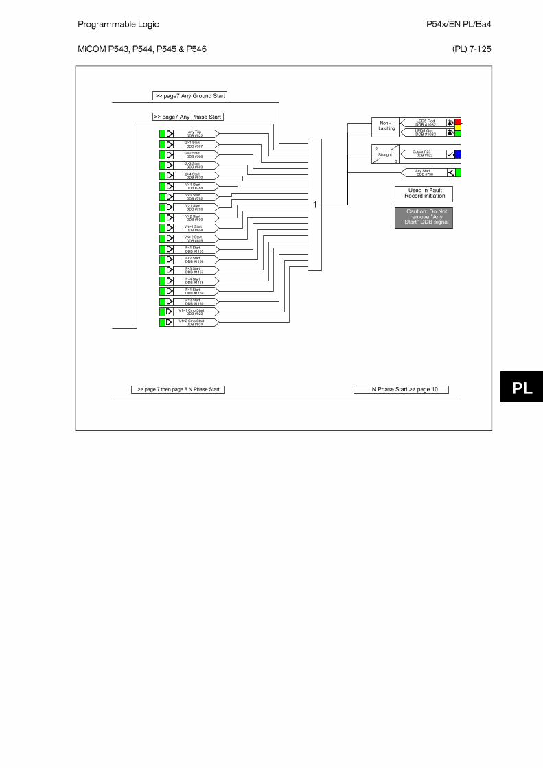
Programmable Logic P54x/EN PL/Ba4 MiCOM P543, P544, P545 & P546
(PL) 7-125
PL
DDB #788V<1 Start
DDB #792V<2 Start
DDB #796V>1 Start
DDB #800V>2 Start
DDB #804VN>1 Start
DDB #805VN>2 Start
DDB #736Any Start
1
Used in Fault Record initiation
Caution: Do Not remove "Any
Start" DDB signal
DDB #1032Non -Latching
LED5 Red
DDB #1033LED5 Grn
>> page7 Any Ground Start
>> page7 Any Phase Start
DDB #522Any Trip
Straight0
0
Output R23DDB #022
DDB #567I2>1 Start
DDB #568I2>2 Start
DDB #569I2>3 Start
DDB #570I2>4 Start
DDB #1155F<1 Start
DDB #1156F<2 Start
DDB #1157F<3 Start
DDB #1158F<4 Start
DDB #1159F>1 Start
DDB #1160F>2 Start
DDB #923V1>1 Cmp Start
DDB #924V1>2 Cmp Start
>> page 7 then page 8 N Phase Start N Phase Start >> page 10

P54x/EN PL/Ba4 Programmable Logic
(PL) 7-126
MiCOM P543, P544, P545 & P546
PL
DDB #609Zone 1 A Trip
1 DDB #952Faulted Phase A
DDB #614Zone 2 A Trip
DDB #619Zone 3 A Trip
DDB #624Zone P A Trip
DDB #629Zone 4 A Trip
DDB #633Aided 1 Trip A
DDB #643Aided 2 Trip A
DDB #647Aid 2 WI Trip A
DDB #637Aid 1 WI Trip A
DDB #656I>1 Trip A
DDB #660I>2 Trip A
DDB #664I>3 Trip A
DDB #668I>4 Trip A
DDB #577AR Trip Test A
DDB #610Zone 1 B Trip
DDB #615Zone 2 B Trip
DDB #620Zone 3 B Trip
DDB #630Zone 4 B Trip
DDB #625Zone P B Trip
DDB #634Aided 1 Trip B
DDB #644Aided 2 Trip B
DDB #638Aid 1 WI Trip B
DDB #648Aid 2 WI Trip B
DDB #657I>1 Trip B
DDB #661I>2 Trip B
DDB #665I>3 Trip B
DDB #669I>4 Trip B
DDB #578AR Trip Test B
1 DDB #953Faulted Phase B
DDB #583Diff Trip A
DDB #588Diff InterTrip B
DDB #584Diff Trip B
DDB #587Diff InterTrip A
>> page 7 then page 8 N Phase Start N Phase Start >> page 10
Faulted Phase Flag, Used in Fault record and on LCD display.
Caution: Do Not remove "Faulted
Phase" DDB signals
DDB #576AR Trip Test
DDB #576AR Trip Test

Programmable Logic P54x/EN PL/Ba4 MiCOM P543, P544, P545 & P546
(PL) 7-127
PL 1 DDB #955Faulted Phase N
DDB #612Zone 1 N Trip
DDB #617Zone 2 N Trip
DDB #622Zone 3 N Trip
DDB #627Zone P N Trip
DDB #632Zone 4 N Trip
DDB #636Aided 1 Trip N
DDB #646Aided 2 Trip N
DDB #671IN>1 Trip
DDB #672IN>2 Trip
DDB #673IN>3 Trip
DDB #674IN>4 Trip
DDB #700VN>1 Trip
DDB #701VN>2 Trip
DDB #611Zone 1 C Trip
DDB #621Zone 3 C Trip
DDB #626Zone P C Trip
DDB #631Zone 4 C Trip
DDB #635Aided 1 Trip C
DDB #639Aid 1 WI Trip C
DDB #645Aided 2 Trip C
DDB #649Aid 2 WI Trip C
DDB #658I>1 Trip C
DDB #662I>2 Trip C
DDB #666I>3 Trip C
DDB #670I>4 Trip C
DDB #579AR Trip Test C
1 DDB #954Faulted Phase C
DDB #675ISEF>1 Trip
DDB #676ISEF>2 Trip
DDB #677ISEF>3 Trip
DDB #678ISEF>4 Trip
DDB #589Diff InterTrip C
DDB #585Diff Trip C
DDB #616Zone 2 C Trip
Faulted Phase Flag, Used in Fault record and on LCD display.
Caution: Do Not remove "Faulted
Phase" DDB signals
>> page 7 then page 8 the page 9 N Phase Start
DDB #576AR Trip Test

P54x/EN PL/Ba4 Programmable Logic
(PL) 7-128
MiCOM P543, P544, P545 & P546
PL
DDB #609Zone 1 A Trip
DDB #633Aided 1 Trip A
DDB #637Aid 1 WI Trip A
DDB #643Aided 2 Trip A
DDB #647Aid 2 WI Trip A
DDB #577AR Trip Test A
1 DDB #530Trip Inputs A
DDB #610Zone 1 B Trip
DDB #634Aided 1 Trip B
DDB #638Aid 1 WI Trip B
DDB #644Aided 2 Trip B
DDB #648Aid 2 WI Trip B
DDB #578AR Trip Test B
1 DDB #531Trip Inputs B
DDB #611Zone 1 C Trip
DDB #635Aided 1 Trip C
DDB #639Aid 1 WI Trip C
DDB #645Aided 2 Trip C
DDB #649Aid 2 WI Trip C
DDB #579AR Trip Test C
1 DDB #532Trip Inputs C
DDB #583Diff Trip A
DDB #587Diff InterTrip A
DDB #585Diff Trip C
DDB #589Diff InterTrip C
Inputs to Trip Conversion Logic:These Raw trip signals are then processed in relay fixed logic, to obtain the
correct single, or three pole trip response.
Caution: Do Not remove "Trip Inputs" DDB
signals
DDB #584Diff Trip B
DDB #588Diff InterTrip B
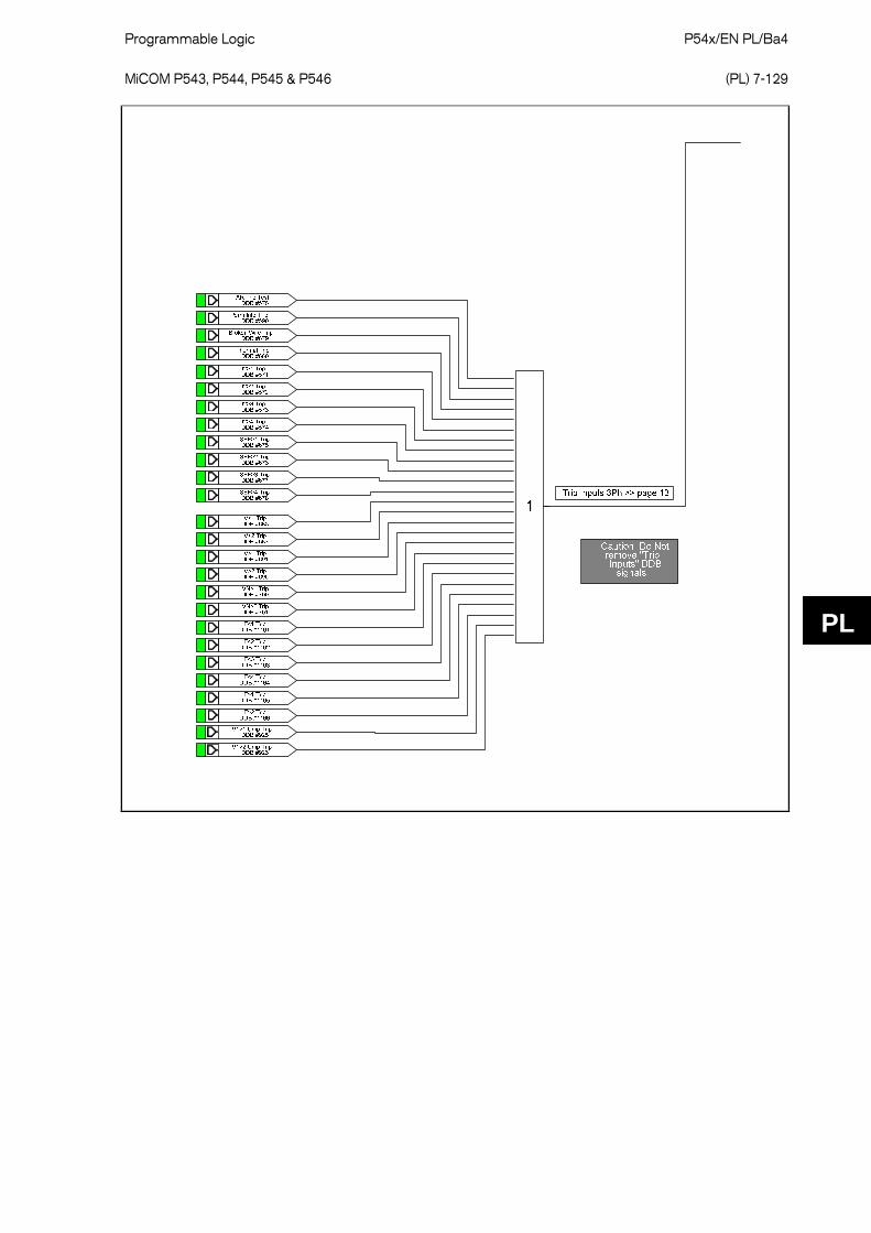
Programmable Logic P54x/EN PL/Ba4 MiCOM P543, P544, P545 & P546
(PL) 7-129
PL

P54x/EN PL/Ba4 Programmable Logic
(PL) 7-130
MiCOM P543, P544, P545 & P546
PL
DDB #613Zone 2 Trip
DDB #618Zone 3 Trip
DDB #623Zone P Trip
DDB #628Zone 4 Trip
DDB #655I>1 Trip
DDB #659I>2 Trip
DDB #663I>3 Trip
DDB #667I>4 Trip
DDB #671IN>1 Trip
DDB #672IN>2 Trip
DDB #673IN>3 Trip
DDB #674IN>4 Trip
DDB #641Aid1 DEF Trip3Ph
DDB #642Aid1 WI Trip 3Ph
DDB #651Aid2 DEF Trip3Ph
DDB #652Aid2 WI Trip 3Ph
DDB #654Loss ofLoad Trip
DDB #699Pole Discrepancy
DDB #704TOR Trip Zone 1
DDB #705TOR Trip Zone 2
DDB #706TOR Trip Zone 3
DDB #708TOR Trip Zone P
DDB #707TOR Trip Zone 4
DDB #709SOTF Trip Zone 1
DDB #710SOTF Trip Zone 2
DDB #711SOTF Trip Zone 3
DDB #713SOTF Trip Zone P
DDB #529Trip Inputs 3Ph1
DDB #712SOTF Trip Zone 4
DDB #591Stub Bus Trip
Caution: Do Not remove "Trip Inputs" DDB
signals
DDB #553OST
DDB #551Pred. OST
DDB #557TOR Trip CNV
DDB #558SOTF Trip CNV
page 12 >> Trip Inputs 3Ph
DDB #640Aid1 Delta Tr3Ph
DDB #650Aid2 Delta Tr3Ph

Programmable Logic P54x/EN PL/Ba4 MiCOM P543, P544, P545 & P546
(PL) 7-131
PL
DDB #886Live Bus &
&
&
1
1
1
DDB #889Dead Line
DDB #887Dead Bus
DDB #888Live Line
DDB #881CS1 Enabled
DDB #882CS2 Enabled
DDB #885SysSplit Enabled
This logic enables Check Synchro to function only for Live Line / Live Bus conditions.
DDB #883Check Sync 1 OK
DDB #884Check Sync 2 OK
DDB #880SysChks Inactive
DDB #898Ctl Check Sync
DDB #899AR Sys Checks OK
Safety Interlock. Logic must be
satisfied before any manual CB closures
can proceed.
DDB #317Aid 1 Chan Fail
DDB #318Aid 2 Chan Fail
DDB #047Input L16
DDB #297Power Swing
DDB #533Force 3Pole Trip
DDB #858AR Force 3 pole
DDB #448BAR
Default PSL blocks Auto-reclose if any
aided scheme channel fails.
DDB #458Inhibit WI
DDB #311Signalling Fail

P54x/EN PL/Ba4 Programmable Logic
(PL) 7-132
MiCOM P543, P544, P545 & P546
PL
MiCOM P545 WITHOUT DISTANCE PROGRAMMABLE SCHEME LOGIC
Output Input Mappings
DDB #032Input L1
DDB #033Input L2
DDB #037Input L6
DDB #038Input L7
DDB #039Input L8
DDB #040Input L9
DDB #041Input L10
DDB #042Input L11
DDB #043Input L12
DDB #044Input L13
DDB #045Input L14
DDB #046Input L15
DDB #049Input L18
DDB #050Input L19
DDB #051Input L20
DDB #052Input L21
DDB #053Input L22
DDB #455Inhibit C Diff
DDB #456Recon Interlock
DDB #535External Trip A
DDB #536External Trip B
DDB #537External Trip C
DDB #425CB Aux A(52-B)
DDB #426CB Aux B(52-B)
DDB #427CB Aux C(52-B)
DDB #438MCB/VTS
DDB #440Init Close CB
DDB #446Reset Lockout
DDB #436CB Healthy
DDB #048Input L17
DDB #453Perm Intertrip
DDB #457Prop Delay Equal
DDB #112IM64 Ch1 Output1
DDB #113IM64 Ch1 Output2
DDB #114IM64 Ch1 Output3
DDB #115IM64 Ch1 Output4
DDB #120IM64 Ch2 Output1
DDB #121IM64 Ch2 Output2
DDB #122IM64 Ch2 Output3
DDB #123IM64 Ch2 Output4
External Trips: Initiate Breaker
Fail, and Auto-reclose (if enabled).
DDB #047Input L16
DDB #448BAR
Opto L5 can be found on other pages

Programmable Logic P54x/EN PL/Ba4 MiCOM P543, P544, P545 & P546
(PL) 7-133
PL
Output Contacts

P54x/EN PL/Ba4 Programmable Logic
(PL) 7-134
MiCOM P543, P544, P545 & P546
PL
Output Contacts
DDB #288SG-opto Invalid
DDB #289Prot'n Disabled
DDB #293VT Fail Alarm
DDB #294CT Fail Alarm
DDB #298CB Fail Alarm
DDB #299CB Monitor Alarm
DDB #300CB Lockout Alarm
DDB #301CB Status Alarm
DDB #291Test Loopback
DDB #292Test IM64
DDB #302CB Trip Fail
DDB #303CB Close Fail
DDB #304Man CB Unhealthy
DDB #305No C/S Man Close
DDB #306A/R Lockout
DDB #307A/R CB Unhealthy
DDB #308A/R No Checksync
DDB #309System Split
DDB #310GPS Alarm
DDB #311Signalling Fail
DDB #312Comm Delay Alarm
DDB #313C Diff Failure
DDB #314IM64 SchemeFail
DDB #315IEEE C37.94 Fail
DDB #319F out of Range
DDB #332Incompatible Rly
DDB #333InValid Mesg Fmt
DDB #334Main Prot. Fail
DDB #335Config Error
DDB #336Re-Config Error
DDB #337Comms Changed
DDB #352Battery Fail
DDB #353Field Volts Fail
1 Dwell
500
0
Output R4DDB #003
General Alarm
DDB #296Remote CT Alarm
DDB #338Max Prop. Alarm

Programmable Logic P54x/EN PL/Ba4 MiCOM P543, P544, P545 & P546
(PL) 7-135
PL
Output Contacts

P54x/EN PL/Ba4 Programmable Logic
(PL) 7-136
MiCOM P543, P544, P545 & P546
PL
LEDs
DDB #522Any Trip
DDB #702Fault REC TRIG
DDB #582Diff Trip
DDB #291Test Loopback
DDB #306A/R Lockout
DDB #844AR 3pole in prog
DDB #845AR 1pole in prog
1
DDB #311Signalling Fail
DDB #1024LatchingLED1 Red
DDB #1025LED1 Grn
DDB #1030Non -Latching
LED4 Red
DDB #1031LED4 Grn
DDB #1034Non -Latching
LED6 Red
DDB #1035LED6 Grn
DDB #1036Non -Latching
LED7 Red
DDB #1037LED7 Grn
DDB #1038Non -Latching
LED8 Red
DDB #1039LED8 Grn
1DDB #586
Diff InterTrip

Programmable Logic P54x/EN PL/Ba4 MiCOM P543, P544, P545 & P546
(PL) 7-137
PL
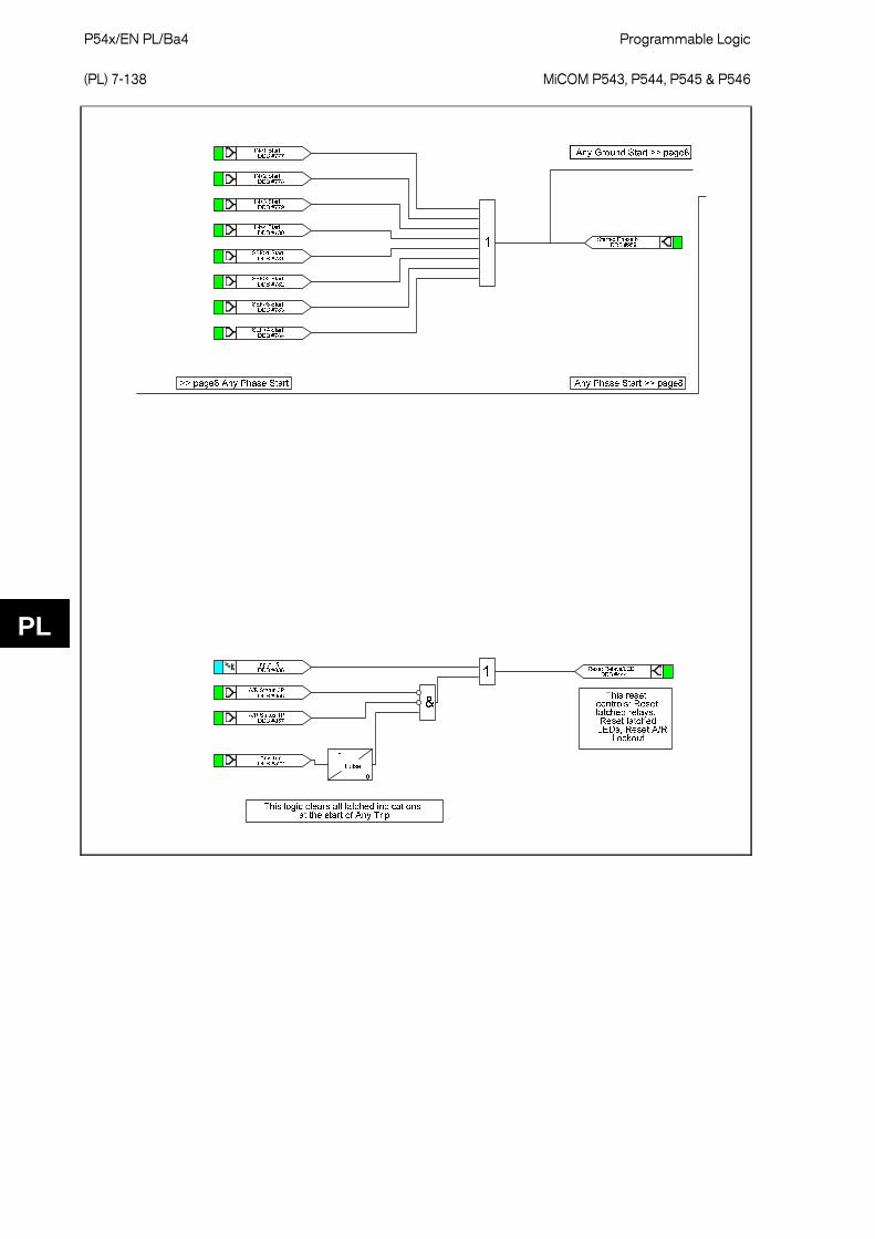
P54x/EN PL/Ba4 Programmable Logic
(PL) 7-138
MiCOM P543, P544, P545 & P546
PL
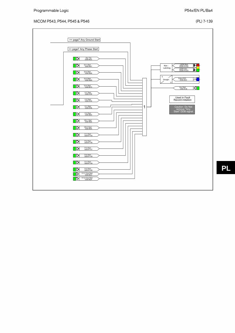
Programmable Logic P54x/EN PL/Ba4 MiCOM P543, P544, P545 & P546
(PL) 7-139
PL
DDB #788V<1 Start
DDB #792V<2 Start
DDB #796V>1 Start
DDB #800V>2 Start
DDB #804VN>1 Start
DDB #805VN>2 Start
DDB #736Any Start
1
>> page7 Any Phase Start
DDB #1032Non -Latching
LED5 Red
DDB #1033LED5 Grn
>> page7 Any Ground Start
DDB #522Any Trip
Straight0
0
Output R23DDB #022
DDB #567I2>1 Start
DDB #568I2>2 Start
DDB #569I2>3 Start
DDB #570I2>4 Start
DDB #1155F<1 Start
DDB #1156F<2 Start
DDB #1157F<3 Start
DDB #1158F<4 Start
DDB #1159F>1 Start
DDB #1160F>2 Start
Used in Fault Record initiation
Caution: Do Not remove "Any
Start" DDB signal
DDB #923V1>1 Cmp Start
DDB #924V1>2 Cmp Start

P54x/EN PL/Ba4 Programmable Logic
(PL) 7-140
MiCOM P543, P544, P545 & P546
PL
1 DDB #952Faulted Phase A
DDB #656I>1 Trip A
DDB #660I>2 Trip A
DDB #664I>3 Trip A
DDB #668I>4 Trip A
DDB #577AR Trip Test A
DDB #657I>1 Trip B
DDB #661I>2 Trip B
DDB #665I>3 Trip B
DDB #669I>4 Trip B
DDB #578AR Trip Test B
1 DDB #953Faulted Phase B
DDB #583Diff Trip A
DDB #588Diff InterTrip B
DDB #584Diff Trip B
DDB #587Diff InterTrip A
Caution: Do Not remove "Faulted Phase" DDB
signals
Faulted Phase Flag, Used in Fault record and on LCD display.
DDB #576AR Trip Test
DDB #576AR Trip Test

Programmable Logic P54x/EN PL/Ba4 MiCOM P543, P544, P545 & P546
(PL) 7-141
PL 1 DDB #955Faulted Phase N
DDB #671IN>1 Trip
DDB #672IN>2 Trip
DDB #673IN>3 Trip
DDB #674IN>4 Trip
DDB #700VN>1 Trip
DDB #701VN>2 Trip
DDB #658I>1 Trip C
DDB #662I>2 Trip C
DDB #666I>3 Trip C
DDB #670I>4 Trip C
DDB #579AR Trip Test C
1 DDB #954Faulted Phase C
DDB #675ISEF>1 Trip
DDB #676ISEF>2 Trip
DDB #677ISEF>3 Trip
DDB #678ISEF>4 Trip
Caution: Do Not remove "Faulted Phase" DDB
signals
DDB #589Diff InterTrip C
DDB #585Diff Trip C
Faulted Phase Flag, Used in Fault record and on LCD display.
DDB #576AR Trip Test

P54x/EN PL/Ba4 Programmable Logic
(PL) 7-142
MiCOM P543, P544, P545 & P546
PL

Programmable Logic P54x/EN PL/Ba4 MiCOM P543, P544, P545 & P546
(PL) 7-143
PL
DDB #576AR Trip Test
DDB #655I>1 Trip
DDB #659I>2 Trip
DDB #663I>3 Trip
DDB #667I>4 Trip
DDB #671IN>1 Trip
DDB #672IN>2 Trip
DDB #673IN>3 Trip
DDB #674IN>4 Trip
DDB #679Broken Wire Trip
DDB #680Thermal Trip
DDB #700VN>1 Trip
DDB #701VN>2 Trip
DDB #699Pole Discrepancy
DDB #683V<1 Trip
DDB #687V<2 Trip
DDB #691V>1 Trip
DDB #695V>2 Trip
DDB #529Trip Inputs 3Ph1
DDB #590Perm InterTrip
DDB #675ISEF>1 Trip
DDB #676ISEF>2 Trip
DDB #677ISEF>3 Trip
DDB #678ISEF>4 Trip
DDB #591Stub Bus Trip
Caution: Do Not remove "Trip Inputs" DDB
signals
DDB #571I2>1 Trip
DDB #572I2>2 Trip
DDB #573I2>3 Trip
DDB #574I2>4 Trip
DDB #1161F<1 Trip
DDB #1162F<2 Trip
DDB #1163F<3 Trip
DDB #1164F<4 Trip
DDB #1165F>1 Trip
DDB #1166F>2 Trip
DDB #925V1>1 Cmp Trip
DDB #926V1>2 Cmp Trip
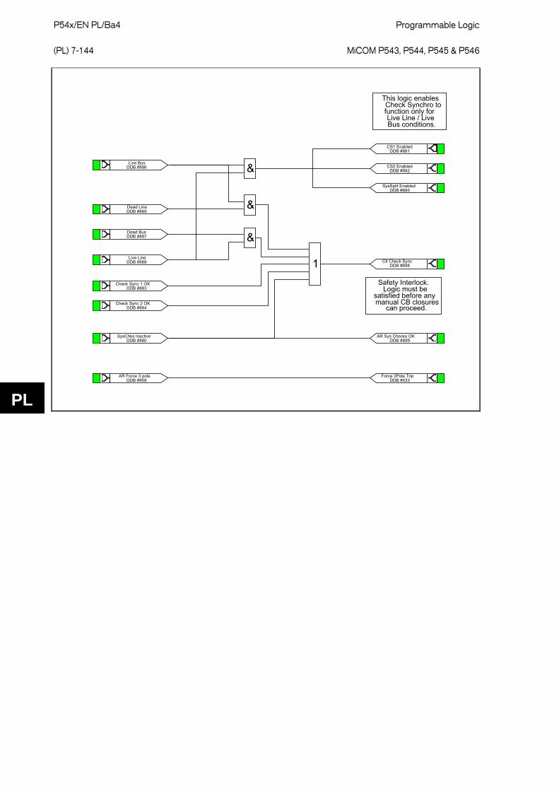
P54x/EN PL/Ba4 Programmable Logic
(PL) 7-144
MiCOM P543, P544, P545 & P546
PL
DDB #886Live Bus
&
&
&
1
DDB #889Dead Line
DDB #887Dead Bus
DDB #888Live Line
DDB #881CS1 Enabled
DDB #882CS2 Enabled
DDB #885SysSplit Enabled
This logic enables Check Synchro to function only for Live Line / Live Bus conditions.
DDB #883Check Sync 1 OK
DDB #884Check Sync 2 OK
DDB #880SysChks Inactive
DDB #898Ctl Check Sync
DDB #899AR Sys Checks OK
Safety Interlock. Logic must be
satisfied before any manual CB closures
can proceed.
DDB #533Force 3Pole Trip
DDB #858AR Force 3 pole

Programmable Logic P54x/EN PL/Ba4 MiCOM P543, P544, P545 & P546
(PL) 7-145
PL
MiCOM P546 WITH DISTANCE PROGRAMMABLE SCHEME LOGIC
Output Input Mappings
DDB #032Input L1
DDB #034Input L3
DDB #035Input L4
DDB #037Input L6
DDB #038Input L7
DDB #039Input L8
DDB #040Input L9
DDB #041Input L10
DDB #042Input L11
DDB #043Input L12
DDB #044Input L13
DDB #045Input L14
DDB #049Input L18
DDB #050Input L19
DDB #051Input L20
DDB #052Input L21
DDB #053Input L22
DDB #455Inhibit C Diff
DDB #493Aided1 Scheme Rx
DDB #492Aided 1 COS/LGS
DDB #425CB1Aux A (52-B)
DDB #426CB1Aux B (52-B)
DDB #427CB1Aux C (52-B)
DDB #438MCB/VTS
DDB #440Init Close CB1
DDB #048Input L17
DDB #112IM64 Ch1 Output1
DDB #120IM64 Ch2 Output1
DDB #433CB2 Aux A(52-B)
DDB #434CB2 Aux B(52-B)
DDB #435CB2 Aux C(52-B)
DDB #047Input L16
DDB #454Stub Bus Enabled
DDB #442Init Close CB2
DDB #046Input L15
DDB #436CB1 Healthy
DDB #437CB2 Healthy
DDB #054Input L23
DDB #055Input L24
DDB #535CB1 Ext Trip A
DDB #536CB1 Ext Trip B
DDB #537CB1 Ext Trip C
DDB #539CB2 Ext Trip A
DDB #540CB2 Ext Trip B
DDB #541CB2 Ext Trip C
DDB #033Input L2
DDB #1421Block CB2 AR
DDB #448Block CB1 AR

P54x/EN PL/Ba4 Programmable Logic
(PL) 7-146
MiCOM P543, P544, P545 & P546
PL
Output Contacts
DDB #523CB1 Trip OutputA
DDB #524CB1 Trip OutputB
DDB #525CB1 Trip OutputC
Dwell
100
0
Output R9DDB #008
Dwell
100
0
Output R10DDB #009
Dwell
100
0
Output R11DDB #010
Straight0
0
Output R1DDB #000
Straight
0
0
Output R2DDB #001
Dwell
100
0
Output R3DDB #002
Straight
0
0
Output R5DDB #004
Dwell100
0
Output R6DDB #005
Straight0
0
Output R7DDB #006
Straight0
0
Output R8DDB #007
DDB #608Zone 1 Trip
DDB #311Signalling Fail
DDB #522Any Trip
DDB #096IM64 Ch1 Input 1
DDB #104IM64 Ch2 Input 1
1
DDB #834CB1 Fail1 Trip
DDB #839Control CloseCB1
DDB #838Control TripCB1
Dwell100
0
Output R12DDB #011
Straight
0
0
Output R13DDB #012
Straight
0
0
Output R14DDB #013
Dwell
100
0
Output R15DDB #014
Dwell
100
0
Output R16DDB #015
DDB #840Control TripCB2
DDB #836CB2 Fail1 Trip
DDB #837CB2 Fail2 Trip
DDB #841Control CloseCB2
DDB #835CB1 Fail2 Trip
Output Contacts
Trip Outputs are
generated by the internal single/three phase trip conversion
logic.

Programmable Logic P54x/EN PL/Ba4 MiCOM P543, P544, P545 & P546
(PL) 7-147
PL
Output Contacts
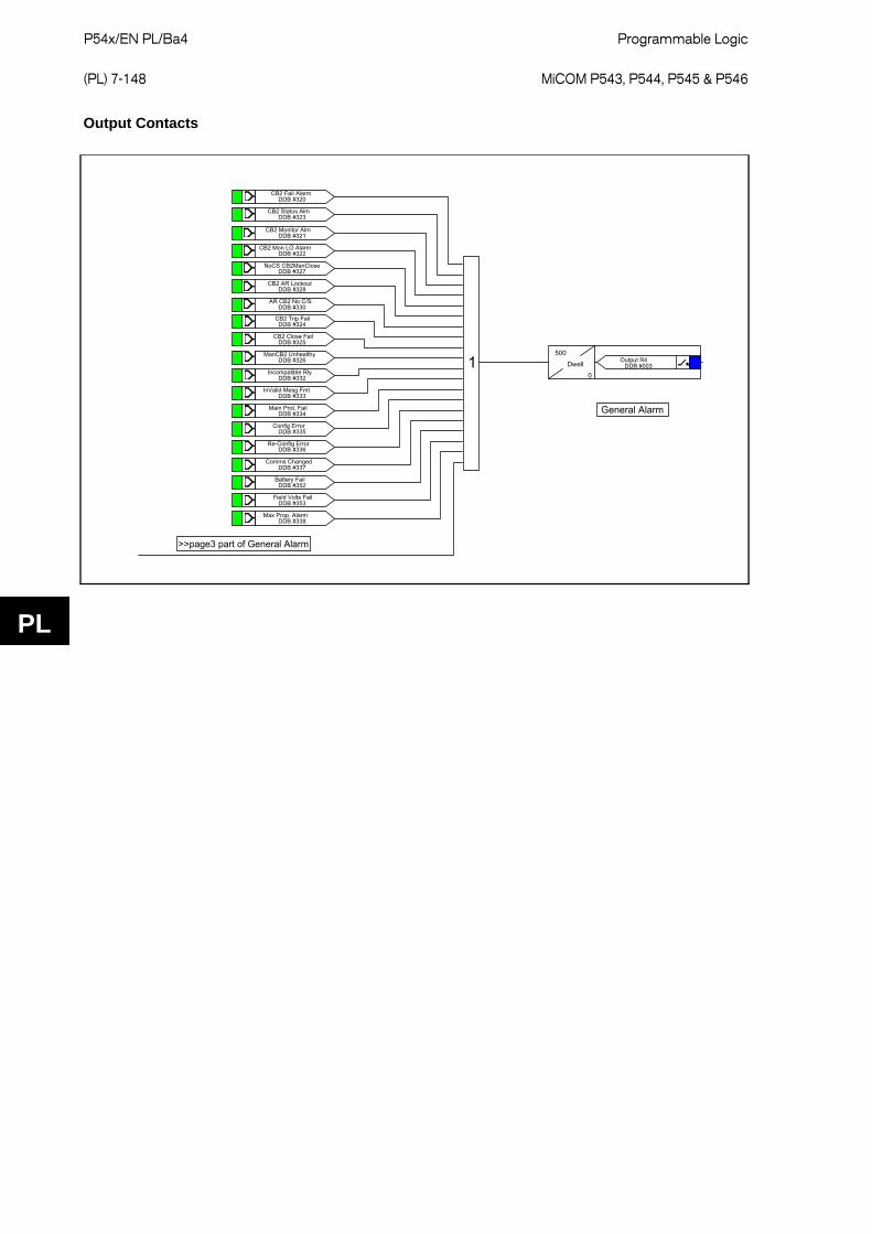
P54x/EN PL/Ba4 Programmable Logic
(PL) 7-148
MiCOM P543, P544, P545 & P546
PL
Output Contacts
DDB #332Incompatible Rly
DDB #333InValid Mesg Fmt
DDB #334Main Prot. Fail
DDB #335Config Error
DDB #336Re-Config Error
DDB #337Comms Changed
DDB #352Battery Fail
DDB #353Field Volts Fail
Dwell
500
0
Output R4DDB #003
DDB #320CB2 Fail Alarm
DDB #323CB2 Status Alm
DDB #324CB2 Trip Fail
DDB #325CB2 Close Fail
DDB #326ManCB2 Unhealthy
DDB #338Max Prop. Alarm
DDB #321CB2 Monitor Alm
DDB #322CB2 Mon LO Alarm
DDB #327NoCS CB2ManClose
DDB #328CB2 AR Lockout
DDB #330AR CB2 No C/S
1
General Alarm
>>page3 part of General Alarm

Programmable Logic P54x/EN PL/Ba4 MiCOM P543, P544, P545 & P546
(PL) 7-149
PL
Output Contacts
DDB #505Aid 1 DEF Trip
DDB #521Aid 2 DEF Trip 1 Straight
0
0
Output R22DDB #021
DDB #498Aided 1 Send
Straight
0
0
Output R24DDB #023
Dwell
100
0
Output R17DDB #016
Dwell
100
0
Output R18DDB #017
Dwell
100
0
Output R19DDB #018
Straight
0
0
Output R20DDB #019
Straight
0
0
Output R21DDB #020
Straight
0
0
Output R25DDB #024
Straight
0
0
Output R26DDB #025
Straight
0
0
Output R27DDB #026
Straight
0
0
Output R28DDB #027
Straight
0
0
Output R29DDB #028
Straight
0
0
Output R30DDB #029
Straight
0
0
Output R31DDB #030
DDB #582Diff Trip
DDB #608Zone 1 Trip
DDB #503Aid 1 Dist Trip
DDB #519Aid 2 Dist Trip
1
DDB #613Zone 2 Trip
DDB #618Zone 3 Trip
DDB #623Zone P Trip
DDB #628Zone 4 Trip
1
1
DDB #293VT Fail Alarm
DDB #297Power Swing
DDB #310GPS Alarm
DDB #586Diff InterTrip
DDB #1601CB2 Trip OutputA
DDB #1602CB2 Trip OutputB
DDB #1603CB2 Trip OutputC
DDB #306CB1 AR Lockout
DDB #328CB2 AR Lockout
DDB #1542ARIP
DDB #852CB1 Succ 3P AR
DDB #1451CB2 Succ 1P AR
DDB #1571CB1 Succ 1P AR
DDB #1452CB2 Succ 3P AR
Straight
0
0
Output R32DDB #0311
Trip Outputs are
generated by the internal single/three phase trip conversion
logic.

P54x/EN PL/Ba4 Programmable Logic
(PL) 7-150
MiCOM P543, P544, P545 & P546
PL
DDB #741Zone 1 A Start
DDB #745Zone 2 A Start
DDB #749Zone 3 A Start
DDB #753Zone P A Start
DDB #757Zone 4 A Start
DDB #762I>1 Start A
DDB #766I>2 Start A
1
DDB #770I>3 Start A
DDB #774I>4 Start A
DDB #742Zone 1 B Start
DDB #746Zone 2 B Start
DDB #750Zone 3 B Start
DDB #754Zone P B Start
DDB #758Zone 4 B Start
DDB #763I>1 Start B
DDB #767I>2 Start B
DDB #771I>3 Start B
DDB #775I>4 Start B
1
DDB #743Zone 1 C Start
DDB #747Zone 2 C Start
DDB #751Zone 3 C Start
DDB #755Zone P C Start
DDB #759Zone 4 C Start
DDB #764I>1 Start C
DDB #768I>2 Start C
DDB #772I>3 Start C
DDB #776I>4 Start C
1
DDB #956Started Phase A
1Any Phase Start >>page7
DDB #957Started Phase B
DDB #958Started Phase C
DDB #738Diff Start A
DDB #739Diff Start B
DDB #740Diff Start C
Any Phase Start >>page7Any Phase Start >>page7
Start Phase Mappings. Used in Fault Record &
on LCD Display
Caution: Do Not remove "Started
Phase" DDB signals

Programmable Logic P54x/EN PL/Ba4 MiCOM P543, P544, P545 & P546
(PL) 7-151
PL
DDB #744Zone 1 N Start
DDB #748Zone 2 N Start
DDB #752Zone 3 N Start
DDB #760Zone 4 N Start
DDB #777IN>1 Start
DDB #778IN>2 Start
DDB #780IN>4 Start
1
Any Ground Start >> page8
DDB #1013Phase Select N
DDB #522Any Trip
&
DDB #036Input L5
DDB #1013Phase Select N
DDB #522Any Trip
Pulse
10
0
&
1
DDB #959Started Phase N
DDB #444Reset Relays/LED
DDB #781ISEF>1 Start
DDB #782ISEF>2 Start
DDB #783ISEF>3 Start
DDB #784ISEF>4 Start
Any Ground Start >> page8Any Ground Start >> page8
DDB #756Zone P N Start
Any Phase Start >> page8>>page6 Any Phase Start
N Phase Start >> page8 then page 9 then page 10
This logic ensures correct N indications for faults involving ground. The pulse prevents pole
scatter affecting the N indication.
This logic clears all latched indications at the start of Any Trip
This reset controls: Reset latched relays, Reset latched
LEDs.
DDB #1385AR In Service &
DDB #779IN>3 Start
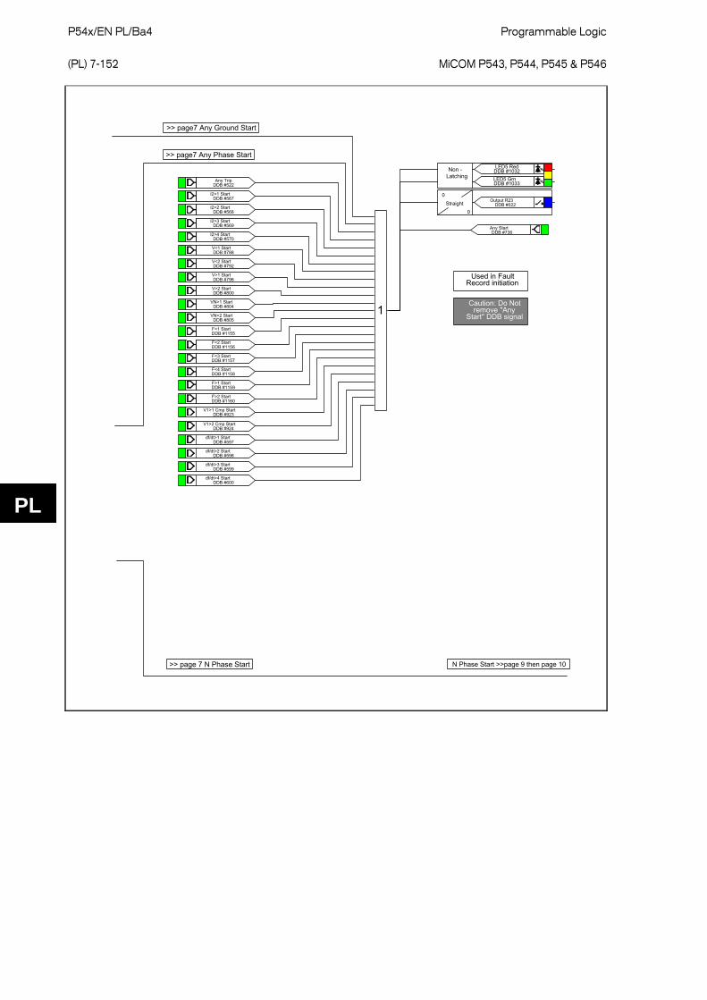
P54x/EN PL/Ba4 Programmable Logic
(PL) 7-152
MiCOM P543, P544, P545 & P546
PL
DDB #788V<1 Start
DDB #792V<2 Start
DDB #796V>1 Start
DDB #800V>2 Start
DDB #804VN>1 Start
DDB #805VN>2 Start
DDB #736Any Start
1
>> page7 Any Phase Start
DDB #1032Non -Latching
LED5 Red
DDB #1033LED5 Grn
DDB #522Any Trip
>> page7 Any Ground Start
Straight
0
0
Output R23DDB #022
DDB #567I2>1 Start
DDB #568I2>2 Start
DDB #569I2>3 Start
DDB #570I2>4 Start
DDB #1155F<1 Start
DDB #1156F<2 Start
DDB #1157F<3 Start
DDB #1158F<4 Start
DDB #1159F>1 Start
DDB #1160F>2 Start
>> page 7 N Phase Start
Caution: Do Not remove "Any
Start" DDB signal
Used in Fault Record initiation
DDB #923V1>1 Cmp Start
DDB #924V1>2 Cmp Start
DDB #597df/dt>1 Start
DDB #598df/dt>2 Start
DDB #599df/dt>3 Start
DDB #600df/dt>4 Start
N Phase Start >>page 9 then page 10

Programmable Logic P54x/EN PL/Ba4 MiCOM P543, P544, P545 & P546
(PL) 7-153
PL
DDB #609Zone 1 A Trip
1 DDB #952Faulted Phase A
DDB #614Zone 2 A Trip
DDB #619Zone 3 A Trip
DDB #624Zone P A Trip
DDB #629Zone 4 A Trip
DDB #633Aided 1 Trip A
DDB #643Aided 2 Trip A
DDB #647Aid 2 WI Trip A
DDB #637Aid 1 WI Trip A
DDB #656I>1 Trip A
DDB #660I>2 Trip A
DDB #664I>3 Trip A
DDB #668I>4 Trip A
DDB #610Zone 1 B Trip
DDB #615Zone 2 B Trip
DDB #620Zone 3 B Trip
DDB #630Zone 4 B Trip
DDB #625Zone P B Trip
DDB #634Aided 1 Trip B
DDB #644Aided 2 Trip B
DDB #638Aid 1 WI Trip B
DDB #648Aid 2 WI Trip B
DDB #657I>1 Trip B
DDB #661I>2 Trip B
DDB #665I>3 Trip B
DDB #669I>4 Trip B
1 DDB #953Faulted Phase B
DDB #583Diff Trip A
DDB #588Diff InterTrip B
DDB #584Diff Trip B
DDB #587Diff InterTrip A
>> page 7 then page 8 N Phase Start N Phase Start >> page 10
Faulted Phase Flag, Used in Fault record and on LCD display.
Caution: Do Not remove "Faulted
Phase" DDB signals
DDB #577AR Trip Test A
DDB #578AR Trip Test B

P54x/EN PL/Ba4 Programmable Logic
(PL) 7-154
MiCOM P543, P544, P545 & P546
PL
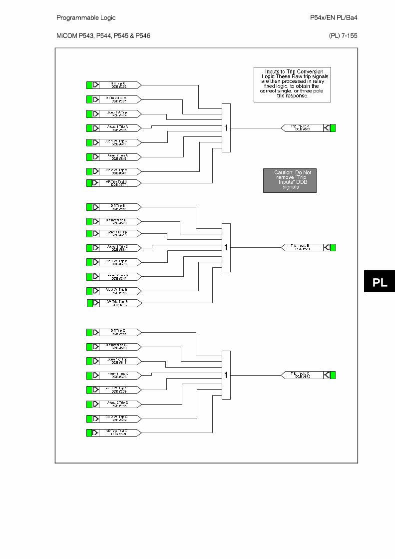
Programmable Logic P54x/EN PL/Ba4 MiCOM P543, P544, P545 & P546
(PL) 7-155
PL

P54x/EN PL/Ba4 Programmable Logic
(PL) 7-156
MiCOM P543, P544, P545 & P546
PL
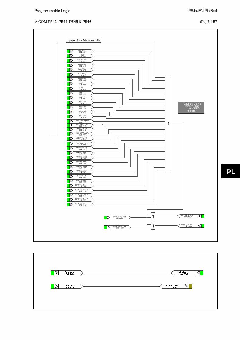
Programmable Logic P54x/EN PL/Ba4 MiCOM P543, P544, P545 & P546
(PL) 7-157
PL
DDB #613Zone 2 Trip
DDB #618Zone 3 Trip
DDB #623Zone P Trip
DDB #628Zone 4 Trip
DDB #655I>1 Trip
DDB #659I>2 Trip
DDB #663I>3 Trip
DDB #667I>4 Trip
DDB #671IN>1 Trip
DDB #672IN>2 Trip
DDB #673IN>3 Trip
DDB #674IN>4 Trip
DDB #641Aid1 DEF Trip3Ph
DDB #642Aid1 WI Trip 3Ph
DDB #651Aid2 DEF Trip3Ph
DDB #652Aid2 WI Trip 3Ph
DDB #654Loss ofLoad Trip
DDB #704TOR Trip Zone 1
DDB #705TOR Trip Zone 2
DDB #706TOR Trip Zone 3
DDB #708TOR Trip Zone P
DDB #707TOR Trip Zone 4
DDB #709SOTF Trip Zone 1
DDB #710SOTF Trip Zone 2
DDB #711SOTF Trip Zone 3
DDB #713SOTF Trip Zone P
DDB #529CB1 Trip I/P 3Ph
1
DDB #712SOTF Trip Zone 4
DDB #591Stub Bus Trip
DDB #553OST
DDB #551Pred. OST
DDB #557TOR Trip CNV
DDB #558SOTF Trip CNV
page 12 >> Trip Inputs 3Ph
Caution: Do Not remove "Trip Inputs" DDB
signals
DDB #1608CB2 Trip I/P 3Ph
1
1
DDB #699Pole Discrep.CB1
DDB #1607Pole Discrep.CB2
DDB #640Aid1 Delta Tr3Ph
DDB #650Aid2 Delta Tr3Ph

P54x/EN PL/Ba4 Programmable Logic
(PL) 7-158
MiCOM P543, P544, P545 & P546
PL
LEDs
DDB #582Diff Trip
DDB #291Test Loopback
1
1
DDB #608Zone 1 Trip
DDB #503Aid 1 Dist Trip
DDB #519Aid 2 Dist Trip
DDB #613Zone 2 Trip
DDB #618Zone 3 Trip
DDB #623Zone P Trip
DDB #628Zone 4 Trip
DDB #311Signalling Fail
DDB #1024LatchingLED1 Red
DDB #1025LED1 Grn
DDB #1026LatchingLED2 Red
DDB #1027LED2 Grn
DDB #1028Latching
LED3 Red
DDB #1029LED3 Grn
DDB #1030Non -Latching
LED4 Red
DDB #1038Non -Latching
LED8 Red
DDB #1039LED8 Grn
1DDB #586
Diff InterTrip
LEDs
DDB #1036Non -Latching
LED7 Red
DDB #1037LED7 Grn
DDB #1385AR In Service
DDB #1040Non -Latching
FnKey LED1 Red
DDB #1041FnKey LED1 Grn
DDB #1042Non -Latching
FnKey LED2 Red
DDB #1043FnKey LED2 Grn
DDB #1044Non -Latching
FnKey LED3 Red
DDB #1045FnKey LED3 Grn
DDB #1046Non -Latching
FnKey LED4 Red
DDB #1047FnKey LED4 Grn
DDB #1048Non -Latching
FnKey LED5 Red
DDB #1049FnKey LED5 Grn
DDB #1050Non -Latching
FnKey LED6 Red
DDB #1051FnKey LED6 Grn
DDB #1052Non -Latching
FnKey LED7 Red
DDB #1053FnKey LED7 Grn
DDB #1054Non -Latching
FnKey LED8 Red
DDB #1055FnKey LED8 Grn
DDB #1056Non -Latching
FnKey LED9 Red
DDB #1057FnKey LED9 Grn
DDB #1058Non -Latching
FnKey LED10 Red
DDB #1059FnKey LED10 Grn
DDB #904CB1 Open A ph
DDB #905CB1 Open B ph
DDB #906CB1 Open C ph
DDB #908CB1 Closed A ph
DDB #909CB1 Closed B ph
DDB #910CB1 Closed C ph
DDB #306CB1 AR Lockout
DDB #328CB2 AR Lockout
DDB #912CB2 Open A ph
DDB #916CB2 Closed A ph
DDB #913CB2 Open B ph
DDB #917CB2 Closed B ph
DDB #914CB2 Open C ph
DDB #918CB2 Closed C ph
DDB #852CB1 Succ 3P AR
DDB #1571CB1 Succ 1P AR 1
DDB #1544CB1 ARIP
DDB #1435CB2 ARIP
1DDB #1452
CB2 Succ 3P AR
DDB #1451CB2 Succ 1P AR
LED4 GrnDDB #1031

Programmable Logic P54x/EN PL/Ba4 MiCOM P543, P544, P545 & P546
(PL) 7-159
PL
MiCOM P546 WITHOUT DISTANCE PROGRAMMABLE SCHEME LOGIC
Output Input Mappings

P54x/EN PL/Ba4 Programmable Logic
(PL) 7-160
MiCOM P543, P544, P545 & P546
PL
Output Contacts
DDB #523CB1 Trip OutputA
DDB #524CB1 Trip OutputB
DDB #525CB1 Trip OutputC
Dwell100
0
Output R9DDB #008
Dwell100
0
Output R10DDB #009
Dwell100
0
Output R11DDB #010
Straight0
0
Output R2DDB #001
Dwell100
0
Output R3DDB #002
Straight0
0
Output R5DDB #004
Dwell100
0
Output R6DDB #005
Straight0
0
Output R7DDB #006
Straight0
0
Output R8DDB #007
DDB #311Signalling Fail
DDB #522Any Trip
DDB #096IM64 Ch1 Input 1
DDB #104IM64 Ch2 Input 1
1
DDB #834CB1 Fail1 Trip
DDB #839Control CloseCB1
DDB #838Control TripCB1
Dwell100
0
Output R12DDB #011
Straight0
0
Output R13DDB #012
Straight0
0
Output R14DDB #013
Dwell100
0
Output R15DDB #014
Dwell100
0
Output R16DDB #015
DDB #840Control TripCB2
DDB #836CB2 Fail1 Trip
DDB #837CB2 Fail2 Trip
DDB #841Control CloseCB2
DDB #835CB1 Fail2 Trip
Trip Outputs are
generated by the internal single/three phase trip conversion
logic.

Programmable Logic P54x/EN PL/Ba4 MiCOM P543, P544, P545 & P546
(PL) 7-161
PL
Output Contacts
DDB #288SG-opto Invalid
DDB #289Prot'n Disabled
DDB #293VT Fail Alarm
DDB #294CT1 Fail Alarm
DDB #298CB1 Fail Alarm
DDB #301CB1 Status Alm
DDB #291Test Loopback
DDB #292Test IM64
DDB #302CB1 Trip Fail
DDB #303CB1 Close Fail
DDB #304ManCB1 Unhealthy
DDB #310GPS Alarm
DDB #311Signalling Fail
DDB #312Comm Delay Alarm
DDB #313C Diff Failure
DDB #314IM64 SchemeFail
DDB #315IEEE C37.94 Fail
DDB #319F out of Range
1
DDB #295CT2 Fail Alarm
DDB #296Remote CT Alarm
General Alarm
DDB #299CB1 Monitor Alm
DDB #300CB1 Mon LO Alarm
DDB #305NoCS CB1ManClose
DDB #306CB1 AR Lockout
DDB #308AR CB1 No C/S
part of General Alarm >> page4DDB #307AR CB1 Unhealthy

P54x/EN PL/Ba4 Programmable Logic
(PL) 7-162
MiCOM P543, P544, P545 & P546
PL
Output Contacts

Programmable Logic P54x/EN PL/Ba4 MiCOM P543, P544, P545 & P546
(PL) 7-163
PL
Output Contacts
Dwell
100
0
Output R17DDB #016
Dwell
100
0
Output R18DDB #017
Dwell
100
0
Output R19DDB #018
Straight
0
0
Output R25DDB #024
Straight
0
0
Output R26DDB #025
Straight
0
0
Output R27DDB #026
Straight
0
0
Output R29DDB #028
Straight
0
0
Output R30DDB #029
Straight
0
0
Output R31DDB #030
DDB #582Diff Trip
1
DDB #293VT Fail Alarm
DDB #310GPS Alarm
DDB #586Diff InterTrip
DDB #1601CB2 Trip OutputA
DDB #1602CB2 Trip OutputB
DDB #1603CB2 Trip OutputC
DDB #306CB1 AR Lockout
DDB #328CB2 AR Lockout
DDB #1542ARIP
DDB #852CB1 Succ 3P AR
DDB #1451CB2 Succ 1P AR
DDB #1571CB1 Succ 1P AR
DDB #1452CB2 Succ 3P AR
Straight
0
0
Output R32DDB #0311
Trip Outputs are
generated by the internal single/three phase trip conversion
logic.

P54x/EN PL/Ba4 Programmable Logic
(PL) 7-164
MiCOM P543, P544, P545 & P546
PL
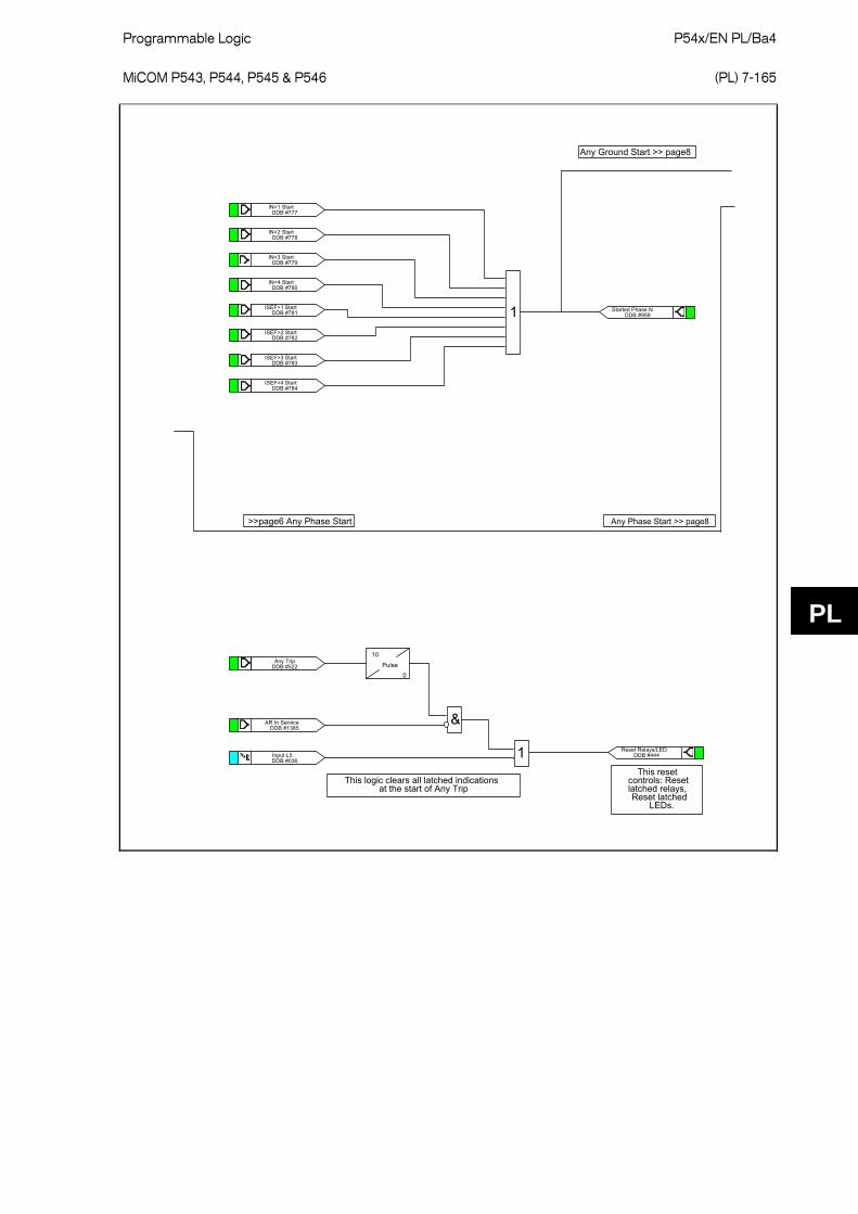
Programmable Logic P54x/EN PL/Ba4 MiCOM P543, P544, P545 & P546
(PL) 7-165
PL
DDB #777IN>1 Start
DDB #778IN>2 Start
DDB #780IN>4 Start
1
DDB #036Input L5
DDB #522Any Trip
Pulse
10
0
1
DDB #959Started Phase N
DDB #444Reset Relays/LED
DDB #781ISEF>1 Start
DDB #782ISEF>2 Start
DDB #783ISEF>3 Start
DDB #784ISEF>4 Start
Any Phase Start >> page8>>page6 Any Phase Start
This logic clears all latched indications at the start of Any Trip
This reset controls: Reset latched relays, Reset latched
LEDs.
DDB #779IN>3 Start
DDB #1385AR In Service &
Any Ground Start >> page8

P54x/EN PL/Ba4 Programmable Logic
(PL) 7-166
MiCOM P543, P544, P545 & P546
PL
DDB #788V<1 Start
DDB #792V<2 Start
DDB #796V>1 Start
DDB #800V>2 Start
DDB #804VN>1 Start
DDB #805VN>2 Start
DDB #736Any Start
1
>> page7 Any Phase Start
DDB #1032Non -Latching
LED5 Red
DDB #1033LED5 Grn
DDB #522Any Trip
>> page7 Any Ground Start
Straight0
0
Output R23DDB #022
DDB #567I2>1 Start
DDB #568I2>2 Start
DDB #569I2>3 Start
DDB #570I2>4 Start
DDB #1155F<1 Start
DDB #1156F<2 Start
DDB #1157F<3 Start
DDB #1158F<4 Start
DDB #1159F>1 Start
DDB #1160F>2 Start
Caution: Do Not remove "Any
Start" DDB signal
Used in Fault Record initiation
DDB #923V1>1 Cmp Start
DDB #924V1>2 Cmp Start
DDB #597df/dt>1 Start
DDB #598df/dt>2 Start
DDB #599df/dt>3 Start
DDB #600df/dt>4 Start

Programmable Logic P54x/EN PL/Ba4 MiCOM P543, P544, P545 & P546
(PL) 7-167
PL

P54x/EN PL/Ba4 Programmable Logic
(PL) 7-168
MiCOM P543, P544, P545 & P546
PL 1 DDB #955
Faulted Phase N
DDB #671IN>1 Trip
DDB #672IN>2 Trip
DDB #673IN>3 Trip
DDB #674IN>4 Trip
DDB #700VN>1 Trip
DDB #701VN>2 Trip
DDB #658I>1 Trip C
DDB #662I>2 Trip C
DDB #666I>3 Trip C
DDB #670I>4 Trip C
1 DDB #954Faulted Phase C
DDB #675ISEF>1 Trip
DDB #676ISEF>2 Trip
DDB #677ISEF>3 Trip
DDB #678ISEF>4 Trip
DDB #589Diff InterTrip C
DDB #585Diff Trip C
Faulted Phase Flag, Used in Fault record and on LCD display.
Caution: Do Not remove "Faulted
Phase" DDB signals
DDB #579AR Trip Test C

Programmable Logic P54x/EN PL/Ba4 MiCOM P543, P544, P545 & P546
(PL) 7-169
PL

P54x/EN PL/Ba4 Programmable Logic
(PL) 7-170
MiCOM P543, P544, P545 & P546
PL

Programmable Logic P54x/EN PL/Ba4 MiCOM P543, P544, P545 & P546
(PL) 7-171
PL

P54x/EN PL/Ba4 Programmable Logic
(PL) 7-172
MiCOM P543, P544, P545 & P546
PL
LEDs

Measurements and Recording P54x/EN MR/Ba4 MiCOM P543, P544, P545 & P546
MR
MEASUREMENTS AND RECORDING
Date: 16th March 2009 Hardware suffix: K Software version:
45 (P543/4/5/6 without Distance) 55 (P543/4/5/6 with Distance)
Connection diagrams: 10P54302 (SH 1 to 2) 10P54303 (SH 1 to 2)
10P54400 10P54404 (SH 1 to 2) 10P54405 (SH 1 to 2)
10P54502 (SH 1 to 2) 10P54503 (SH 1 to 2)
10P54600 10P54604 (SH 1 to 2) 10P54605 (SH 1 to 2) 10P54606 (SH 1 to 2)

P54x/EN MR/Ba4 Measurements and Recording
MiCOM P543, P544, P545 & P546
MR

Measurements and Recording P54x/EN MR/Ba4 MiCOM P543, P544, P545 & P546
(MR) 8-1
MR
CONTENTS
(MR) 8-
1. MEASUREMENTS AND RECORDING 3 1.1 Introduction 3 1.2 Event & fault records 3 1.2.1 Types of event 4 1.2.1.1 Change of state of opto-isolated inputs 4 1.2.1.2 Change of state of one or more output relay contacts 4 1.2.1.3 Relay alarm conditions 4 1.2.1.4 Protection element starts and trips 5 1.2.1.5 General events 5 1.2.1.6 Fault records 5 1.2.1.7 Maintenance reports 5 1.2.1.8 Setting changes 6 1.2.2 Resetting of event/fault records 6 1.2.3 Viewing event records via MiCOM S1 Studio support software 6 1.2.4 Event filtering 7 1.3 Disturbance recorder 8 1.4 Measurements 10 1.4.1 Measured voltages and currents 11 1.4.2 Sequence voltages and currents 11 1.4.3 Slip frequency 11 1.4.4 Power and energy quantities 11 1.4.5 Rms. voltages and currents 12 1.4.6 Demand values 12 1.4.7 Settings 12 1.4.8 Measurement display quantities 13

P54x/EN MR/Ba4 Measurements and Recording
(MR) 8-2
MiCOM P543, P544, P545 & P546
MR

Measurements and Recording P54x/EN MR/Ba4 MiCOM P543, P544, P545 & P546
(MR) 8-3
MR
1. MEASUREMENTS AND RECORDING
1.1 Introduction
The P54x is equipped with integral measurements, event, fault and disturbance recording facilities suitable for analysis of complex system disturbances.
The relay is flexible enough to allow for the programming of these facilities to specific user application requirements and are discussed below.
1.2 Event & fault records
The relay records and time tags up to 512 events and stores them in non-volatile (battery backed up) memory. This enables the system operator to establish the sequence of events that occurred within the relay following a particular power system condition, switching sequence etc. When the available space is exhausted, the oldest event is automatically overwritten by the new one.
The real time clock within the relay provides the time tag to each event, to a resolution of 1ms.
The event records are available for viewing either via the frontplate LCD or remotely, via the communications ports (courier versions only).
Local viewing on the LCD is achieved in the menu column entitled VIEW RECORDS. This column allows viewing of event, fault and maintenance records and is shown in the following table:
VIEW RECORDS
LCD reference Description
Select Event Setting range from 0 to 511. This selects the required event record from the possible 512 that may be stored. A value of 0 corresponds to the latest event and so on.
Time & Date Time & Date Stamp for the event given by the internal Real Time Clock.
Event Text Up to 32 Character description of the Event refer to following sections).
Event Value Up to 32 Bit Binary Flag or integer representative of the Event (refer to following sections).
Select Fault Setting range from 0 to 14. This selects the required fault record from the possible 15 that may be stored. A value of 0 corresponds to the latest fault and so on.
The following cells show all the fault flags, protection starts, protection trips, fault location, measurements etc. associated with the fault, i.e. the complete fault record.
Select Maint. Setting range from 0 to 4. This selects the required maintenance report from the possible 5 that may be stored. A value of 0 corresponds to the latest report and so on.
Maint. Text Up to 16 Character description of the occurrence (refer to following sections).
Maint. Type/Main Data These cells are numbers representative of the occurrence. They form a specific error code which should be quoted in any related correspondence to Report Data.
Reset Indication Either Yes or No. This serves to reset the trip LED indications provided that the relevant protection element has reset.

P54x/EN MR/Ba4 Measurements and Recording
(MR) 8-4
MiCOM P543, P544, P545 & P546
MR
For extraction from a remote source via communications, refer to the SCADA Communications chapter (P54x/EN SC), where the procedure is fully explained.
1.2.1 Types of event
An event may be a change of state of a control input or output relay, an alarm condition, setting change etc. The following sections show the various items that constitute an event:
1.2.1.1 Change of state of opto-isolated inputs
If one or more of the opto (logic) inputs has changed state since the last time that the protection algorithm ran, the new status is logged as an event. When this event is selected to be viewed on the LCD, three applicable cells will become visible as shown below:
Time & date of event
“LOGIC INPUTS 1”
“Event Value 0101010101010101”
The Event Value is an 8, 12, 16 or 24-bit word showing the status of the opto inputs, where the least significant bit (extreme right) corresponds to opto input 1 etc. The same information is present if the event is extracted and viewed via PC.
1.2.1.2 Change of state of one or more output relay contacts
If one or more of the output relay contacts have changed state since the last time that the protection algorithm ran, then the new status is logged as an event. When this event is selected to be viewed on the LCD, three applicable cells will become visible as shown below:
Time & date of event
“OUTPUT CONTACTS 1”
“Event Value 010101010101010101010”
The Event Value is an 8, 12, 16, 24 or 32 bit word showing the status of the output contacts, where the least significant bit (extreme right) corresponds to output contact 1 etc. The same information is present if the event is extracted and viewed via PC.
1.2.1.3 Relay alarm conditions
Any alarm conditions generated by the relays will also be logged as individual events. The following table shows examples of some of the alarm conditions and how they appear in the event list:
Alarm condition Event text Event value
Battery Fail Battery Fail ON/OFF Bit position 0 in 32 bit field
Field Voltage Fail Field Volt Fail ON/OFF Bit position 1 in 32 bit field
Setting Group via Opto Invalid Setting Grp. Invalid ON/OFF Bit position 2 in 32 bit field
Protection Disabled Prot’n. Disabled ON/OFF Bit position 3 in 32 bit field
Frequency out of Range Freq. out of Range ON/OFF Bit position 4 in 32 bit field
VTS Alarm VT Fail Alarm ON/OFF Bit position 5 in 32 bit field
CB Trip Fail Protection CB Fail ON/OFF Bit position 7 in 32 bit field
The previous table shows the abbreviated description that is given to the various alarm conditions and also a corresponding value between 0 and 31. This value is appended to each alarm event in a similar way as for the input and output events previously described. It is used by the event extraction software, such as MiCOM S1, to identify the alarm and is therefore invisible if the event is viewed on the LCD. Either ON or OFF is shown after the description to signify whether the particular condition has become operated or has reset.

Measurements and Recording P54x/EN MR/Ba4 MiCOM P543, P544, P545 & P546
(MR) 8-5
MR
1.2.1.4 Protection element starts and trips
Any operation of protection elements, (either a start or a trip condition) will be logged as an event record, consisting of a text string indicating the operated element and an event value. Again, this value is intended for use by the event extraction software, such as MiCOM S1 Studio, rather than for the user, and is therefore invisible when the event is viewed on the LCD.
1.2.1.5 General events
A number of events come under the heading of ‘General Events’ - an example is shown below:
Nature of event Displayed text in event record Displayed value
Level 1 password modified, either from user interface, front or rear port.
PW1 modified UI, F, R or R2 0 UI=6, F=11, R=16, R2=38
A complete list of the ‘General Events’ is given in the Relay Menu Database (P54x/EN MD), which is a separate document, available for downloading from our website.
1.2.1.6 Fault records
Each time a fault record is generated, an event is also created. The event simply states that a fault record was generated, with a corresponding time stamp.
Note 1: Viewing of the actual fault record is carried out in the Select Fault cell further down the VIEW RECORDS column, which is selectable from up to 15 records. These records consist of fault flags, fault location, fault measurements etc.
Note 2: The time stamp given in the fault record itself will be more accurate than the corresponding stamp given in the event record as the event is logged some time after the actual fault record is generated.
The fault record is triggered from the ‘Fault REC. TRIG.’ signal assigned in the default programmable scheme logic to relay 3, protection trip.
Note: The fault measurements in the fault record are given at the time of the protection start. Also, the fault recorder does not stop recording until any start or relay 3 (protection trip) resets in order to record all the protection flags during the fault.
It is recommended that the triggering contact (relay 3 for example) be ‘self reset’ and not latching. If a latching contact were chosen the fault record would not be generated until the contact had fully reset.
1.2.1.7 Maintenance reports
Internal failures detected by the self-monitoring circuitry, such as watchdog failure, field voltage failure etc. are logged into a maintenance report. The maintenance report holds up to 5 such ‘events’ and is accessed from the Select Report cell at the bottom of the VIEW RECORDS column.
Each entry consists of a self explanatory text string and a ‘Type’ and ‘Data’ cell, which are explained in the menu extract at the beginning of this section.
Each time a Maintenance Report is generated, an event is also created. The event simply states that a report was generated, with a corresponding time stamp.

P54x/EN MR/Ba4 Measurements and Recording
(MR) 8-6
MiCOM P543, P544, P545 & P546
MR
1.2.1.8 Setting changes
Changes to any setting within the relay are logged as an event. Two examples are shown in the following table:
Type of setting change Displayed text in event record Displayed value
Control/Support Setting C & S Changed 22
Group # Change Group # Changed #
Where # = 1 to 4
Note: Control/Support settings are communications, measurement, CT/VT ratio settings etc, which are not duplicated within the four setting groups. When any of these settings are changed, the event record is created simultaneously. However, changes to protection or disturbance recorder settings will only generate an event once the settings have been confirmed at the ‘setting trap’.
1.2.2 Resetting of event/fault records
If it is required to delete either the event, fault or maintenance reports, this may be done from within the RECORD CONTROL column.
1.2.3 Viewing event records via MiCOM S1 Studio support software
When the event records are extracted and viewed on a PC they look slightly different than when viewed on the LCD. The following shows an example of how various events appear when displayed using MiCOM S1 Studio:
- Monday 27 October 2008 15:32:49 GMT Ι>1 Start ON
MiCOM : MiCOM P54x
Model Number: P543218A1M054/50K
Address: 001 Column: 00 Row: 23
Event Type: Protection operation
- Monday 27 October 2008 15:32:52 GMT Fault Recorded
MiCOM : MiCOM P54x
Model Number: P543218A1M054/50K
Address: 001 Column: 01 Row: 00
Event Type: Fault record
- Monday 27 October 2008 15:33:11 GMT Logic Inputs
MiCOM : MiCOM P54x
Model Number: P543218A1M054/50K
Address: 001 Column: 00 Row: 20
Event Type: Logic input changed state
- Monday 27 October 2008 15:34:54 GMT Output Contacts
MiCOM : MiCOM P54x
Model Number: P543218A1M054/50K
Address: 001 Column: 00 Row: 21
Event Type: Relay output changed state

Measurements and Recording P54x/EN MR/Ba4 MiCOM P543, P544, P545 & P546
(MR) 8-7
MR
- Monday 27 October 2008 15:35:55 GMT A/R Lockout ON
MiCOM : MiCOM P54x
Model Number: P543218A1M054/50K
Address: 001 Column: 00 Row: 22
Event Type: Alarm event
- Tuesday 28 October 2008 20:18:22.988 GMT Zone 1 Trip ON
MiCOM : MiCOM P54x
Model Number: P543218A1M054/50K
Address: 001 Column: 0F Row: 30
Event Type: Setting event
As can be seen, the first line gives the description and time stamp for the event, whilst the additional information that is displayed below may be collapsed via the +/– symbol.
For further information regarding events and their specific meaning, refer to Relay Menu Database (P54x/EN MD). This is a standalone document not included in this manual.
1.2.4 Event filtering
It is possible to disable the reporting of events from all interfaces that supports setting changes. The settings that control the various types of events are in the record control column. The effect of setting each to disabled is as follows:
Menu text Default setting Available settings
Clear Event No No or Yes
Selecting “Yes” will cause the existing event log to be cleared and an event will be generated indicating that the events have been erased.
Clear Faults No No or Yes
Selecting “Yes” will cause the existing fault records to be erased from the relay.
Clear Maint. No No or Yes
Selecting “Yes” will cause the existing maintenance records to be erased from the relay.
Alarm Event Enabled Enabled or Disabled
Disabling this setting means that all the occurrences that produce an alarm will result in no event being generated.
Relay O/P Event Enabled Enabled or Disabled
Disabling this setting means that no event will be generated for any change in logic input state.
Opto Input Event Enabled Enabled or Disabled
Disabling this setting means that no event will be generated for any change in logic input state.
General Event Enabled Enabled or Disabled
Disabling this setting means that no General Events will be generated.
Fault Rec. Event Enabled Enabled or Disabled
Disabling this setting means that no event will be generated for any fault that produces a fault record.

P54x/EN MR/Ba4 Measurements and Recording
(MR) 8-8
MiCOM P543, P544, P545 & P546
MR
Menu text Default setting Available settings
Maint. Rec. Event Enabled Enabled or Disabled
Disabling this setting means that no event will be generated for any occurrence that produces a maintenance record.
Protection Event Enabled Enabled or Disabled
Disabling this setting means that any operation of protection elements will not be logged as an event.
Flt Rec Extended Enabled Enabled or Disabled
When this setting is disabled, the fault record contains a snap shot of the local, remote, differential and bias currents taken 1 cycle after the trip.
With this setting enabled an additional snap shot of local, remote, differential and bias currents taken at the time the differential trips is included in the fault record.
DDB 31 - 0 11111111111111111111111111111111
Displays the status of DDB signals 0 - 31.
DDB 1791 - 1760 11111111111111111111111111111111
Displays the status of DDB signals 1791 - 1760
Note: Some occurrences will result in more than one type of event, e.g. a battery failure will produce an alarm event and a maintenance record event.
If the Protection Event setting is Enabled a further set of settings is revealed which allow the event generation by individual DDB signals to be enabled or disabled.
For further information regarding events and their specific meaning, refer to Relay Menu Database document (P54x/EN MD).
1.3 Disturbance recorder
The integral disturbance recorder has an area of memory specifically set aside for record storage. The number of records that may be stored by the relay is dependent upon the selected recording duration. The relay can typically store a minimum of 20 records, each of 1.5 seconds duration. Relays for use with IEC 60870-5 CS 103 communication, however, have the same total record length but the IEC 60870-5 CS 103 communication protocol dictates that only 8 records (of 3 seconds duration) can be extracted via the rear port. Disturbance records continue to be recorded until the available memory is exhausted, at which time the oldest record(s) are overwritten to make space for the newest one.
The recorder stores actual samples that are taken at a rate of 48 samples per cycle.
Each disturbance record consists of twelve analog data channels and thirty-two digital data channels. The relevant CT and VT ratios for the analog channels are also extracted to enable scaling to primary quantities. Note that if a CT ratio is set less than unity, the relay will choose a scaling factor of zero for the appropriate channel.
The DISTURBANCE RECORDER menu column is shown in the following table:

Measurements and Recording P54x/EN MR/Ba4 MiCOM P543, P544, P545 & P546
(MR) 8-9
MR
Setting range Menu text Default setting
Min. Max. Step size
DISTURB. RECORDER
Duration 1.5 s 0.1 s 10.5 s 0.01 s
This sets the overall recording time.
Trigger Position 33.3% 0 100% 0.1%
This sets the trigger point as a percentage of the duration. For example, the default settings show that the overall recording time is set to 1.5 s with the trigger point being at 33.3% of this, giving 0.5 s pre-fault and 1 s post fault recording times.
Trigger Mode Single Single or Extended
If set to single mode, if a further trigger occurs whilst a recording is taking place, the recorder will ignore the trigger. However, if this has been set to Extended, the post trigger timer will be reset to zero, thereby extending the recording time.
Analog. Channel 1 VA
IA, IB, IC, IN, IN Sensitive, VA, VB, VC, IM, V Checksync (for all P54x) and IA2, IB2, IC2, VChecksync2 (only for P544 and P546)
Selects any available analog input to be assigned to this channel (including derived IN residual current).
Analog. Channel 2 VB As above
Analog. Channel 3 VC As above
Analog. Channel 4 ΙA As above
Analog. Channel 5 ΙB As above
Analog. Channel 6 ΙC As above
Analog. Channel 7 ΙN As above
Analog. Channel 8 IN Sensitive As above
Analog. Channel 9 V Checksync As above
Analog. Channel 10 ΙN As above
Analog. Channel 11 ΙN As above
Analog. Channel 12 ΙN As above
Digital Inputs 1 to 32 Relays 1 to 14(32) and Opto’s 1 to 16 (24, or 32)
Any O/P Contact, Any Opto Inputs, or Internal Digital Signals
The digital channels may monitor any of the opto isolated inputs or output contacts, in addition to a number of internal relay digital signals, such as protection starts, LEDs etc.
Inputs 1 to 32 Trigger
No Trigger except Dedicated Trip Relay 3 operation which are set to Trigger L/H
No Trigger, Trigger L/H, Trigger H/L
Any of the digital channels may be selected to trigger the disturbance recorder on either a low to high or a high to low transition.
Analog. Channel 9 V Checksync As above
Analog. Channel 10 ΙM (P543/5)
IA2 (P544/6) As above

P54x/EN MR/Ba4 Measurements and Recording
(MR) 8-10
MiCOM P543, P544, P545 & P546
MR
Setting range Menu text Default setting
Min. Max. Step size
Analog. Channel 11 ΙN (P543/5)
IB2 (P544/6) As above
Analog. Channel 12 ΙN (P543/5)
IC2 (P544/6) As above
The pre and post fault recording times are set by a combination of the Duration and Trigger Position cells. "Duration" sets the overall recording time and the "Trigger Position" sets the trigger point as a percentage of the duration. For example, the default settings show that the overall recording time is set to 1.5 s with the trigger point being at 33.3% of this, giving 0.5 s pre-fault and 1s post fault recording times.
If a further trigger occurs while a recording is taking place, the recorder will ignore the trigger if the Trigger Mode has been set to Single. However, if this has been set to Extended, the post trigger timer will be reset to zero, thereby extending the recording time.
As can be seen from the menu, each of the analog channels is selectable from the available analog inputs to the relay. The digital channels may be mapped to any of the opto isolated inputs or output contacts, in addition to a number of internal relay digital signals, such as protection starts, LEDs etc. The complete list of these signals may be found by viewing the available settings in the relay menu or via a setting file in MiCOM S1 Studio. Any of the digital channels may be selected to trigger the disturbance recorder on either a low to high or a high to low transition, via the Input Trigger cell. The default trigger settings are that any dedicated trip output contacts (e.g. relay 3) will trigger the recorder.
It is not possible to view the disturbance records locally via the LCD; they must be extracted using suitable software such as MiCOM S1 Studio. This process is fully explained in the SCADA Communications chapter (P54x/EN SC).
1.4 Measurements
The relay produces a variety of both directly measured and calculated power system quantities. These measurement values are updated on a per second basis and can be viewed in the Measurements columns (up to three) of the relay or via MiCOM S1 Studio Measurement viewer. The P54x relay is able to measure and display the following quantities as summarized.
• Phase Voltages
• Local and Remote Currents
• Differential and Bias Currents on a Per Phase Basis
• Sequence Voltages and Currents
• Slip Frequency
• Power and Energy Quantities
• Rms. Voltages and Currents
• Peak, Fixed and Rolling Demand Values
There are also measured values from the protection functions, which are also displayed under the measurement columns of the menu; these are described in the section on the relevant protection function.

Measurements and Recording P54x/EN MR/Ba4 MiCOM P543, P544, P545 & P546
(MR) 8-11
MR
1.4.1 Measured voltages and currents
The relay produces both phase to ground and phase to phase voltage and current values. They are produced directly from the DFT (Discrete Fourier Transform) used by the relay protection functions and present both magnitude and phase angle measurement.
Currents mentioned above can be seen on the Measurement 1 column. P54x also shows local and remote currents in Measurement 3 column. These currents have the same treatment as the currents used for differential protection purposes.
1.4.2 Sequence voltages and currents
Sequence quantities are produced by the relay from the measured Fourier values; these are displayed as magnitude and phase angle values.
1.4.3 Slip frequency
The relay produces a slip frequency measurement by measuring the rate of change of phase angle, between the bus and line voltages, over a one-cycle period. The slip frequency measurement assumes the bus voltage to be the reference phasor.
1.4.4 Power and energy quantities
Using the measured voltages and currents the relay calculates the apparent, real and reactive power quantities. These are produced on a phase by phase basis together with three-phase values based on the sum of the three individual phase values. The signing of the real and reactive power measurements can be controlled using the measurement mode setting. The four options are defined in the table below:
Measurement mode Parameter Signing
0
(Default)
Export Power
Import Power
Lagging Vars
Leading VArs
+
–
+
–
1
Export Power
Import Power
Lagging Vars
Leading VArs
–
+
+
–
2
Export Power
Import Power
Lagging Vars
Leading VArs
+
–
–
+
3
Export Power
Import Power
Lagging Vars
Leading VArs
–
+
–
+
In addition to the measured power quantities the relay calculates the power factor on a phase by phase basis in addition to a three-phase power factor.
These power values are also used to increment the total real and reactive energy measurements. Separate energy measurements are maintained for the total exported and imported energy. The energy measurements are incremented up to maximum values of 1000 GWhr or 1000 GVARhr at which point they will reset to zero, it is also possible to reset these values using the menu or remote interfaces using the reset demand cell.
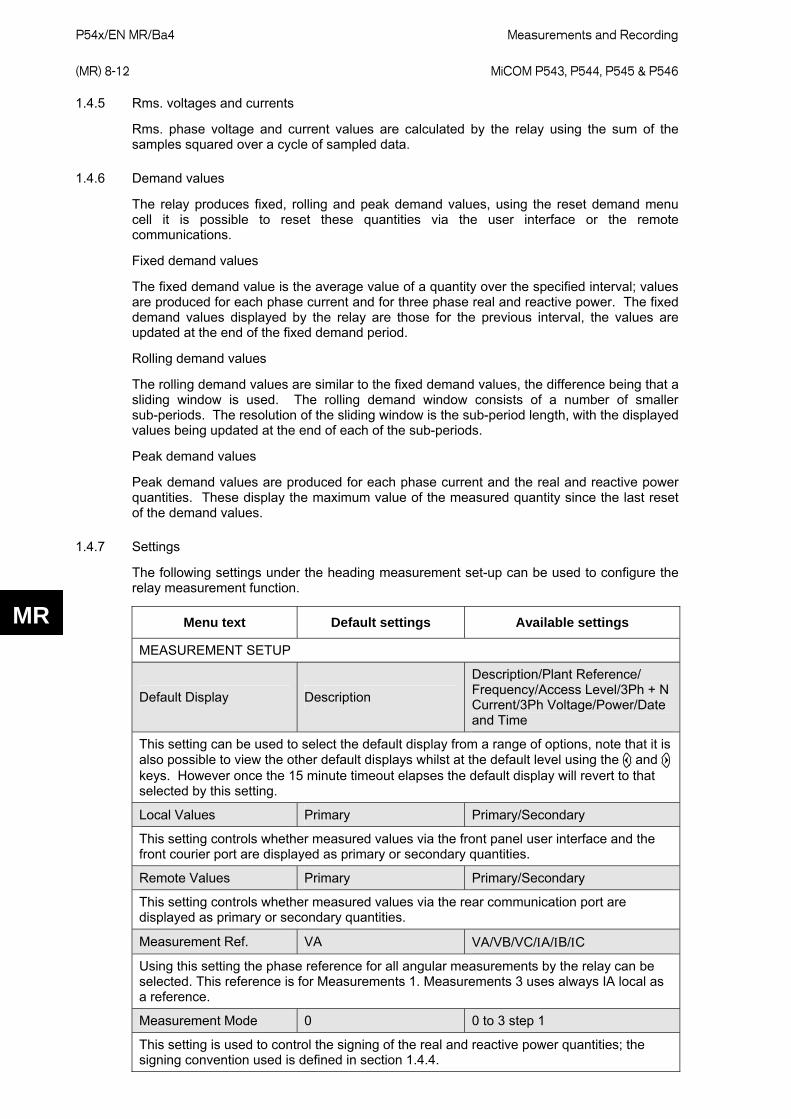
P54x/EN MR/Ba4 Measurements and Recording
(MR) 8-12
MiCOM P543, P544, P545 & P546
MR
1.4.5 Rms. voltages and currents
Rms. phase voltage and current values are calculated by the relay using the sum of the samples squared over a cycle of sampled data.
1.4.6 Demand values
The relay produces fixed, rolling and peak demand values, using the reset demand menu cell it is possible to reset these quantities via the user interface or the remote communications.
Fixed demand values
The fixed demand value is the average value of a quantity over the specified interval; values are produced for each phase current and for three phase real and reactive power. The fixed demand values displayed by the relay are those for the previous interval, the values are updated at the end of the fixed demand period.
Rolling demand values
The rolling demand values are similar to the fixed demand values, the difference being that a sliding window is used. The rolling demand window consists of a number of smaller sub-periods. The resolution of the sliding window is the sub-period length, with the displayed values being updated at the end of each of the sub-periods.
Peak demand values
Peak demand values are produced for each phase current and the real and reactive power quantities. These display the maximum value of the measured quantity since the last reset of the demand values.
1.4.7 Settings
The following settings under the heading measurement set-up can be used to configure the relay measurement function.
Menu text Default settings Available settings
MEASUREMENT SETUP
Default Display Description
Description/Plant Reference/ Frequency/Access Level/3Ph + N Current/3Ph Voltage/Power/Date and Time
This setting can be used to select the default display from a range of options, note that it is also possible to view the other default displays whilst at the default level using the and keys. However once the 15 minute timeout elapses the default display will revert to that selected by this setting.
Local Values Primary Primary/Secondary
This setting controls whether measured values via the front panel user interface and the front courier port are displayed as primary or secondary quantities.
Remote Values Primary Primary/Secondary
This setting controls whether measured values via the rear communication port are displayed as primary or secondary quantities.
Measurement Ref. VA VA/VB/VC/ΙA/ΙB/ΙC
Using this setting the phase reference for all angular measurements by the relay can be selected. This reference is for Measurements 1. Measurements 3 uses always IA local as a reference.
Measurement Mode 0 0 to 3 step 1
This setting is used to control the signing of the real and reactive power quantities; the signing convention used is defined in section 1.4.4.
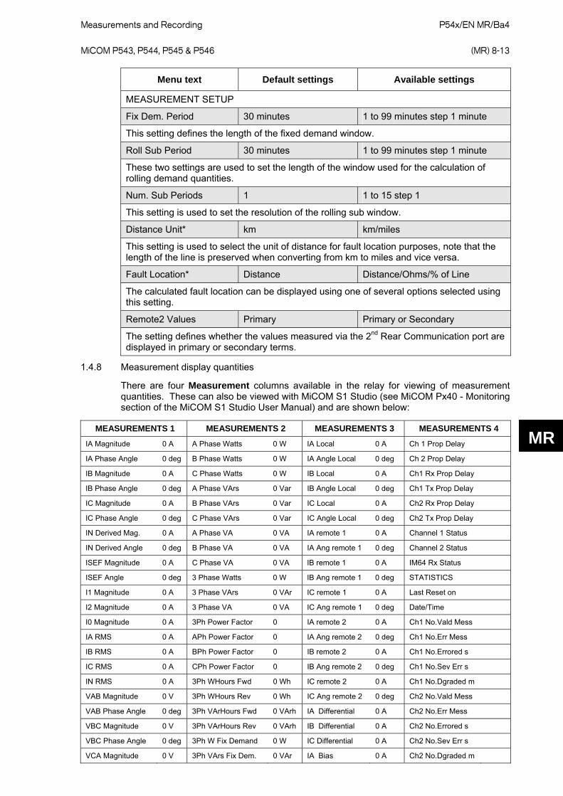
Measurements and Recording P54x/EN MR/Ba4 MiCOM P543, P544, P545 & P546
(MR) 8-13
MR
Menu text Default settings Available settings
MEASUREMENT SETUP
Fix Dem. Period 30 minutes 1 to 99 minutes step 1 minute
This setting defines the length of the fixed demand window.
Roll Sub Period 30 minutes 1 to 99 minutes step 1 minute
These two settings are used to set the length of the window used for the calculation of rolling demand quantities.
Num. Sub Periods 1 1 to 15 step 1
This setting is used to set the resolution of the rolling sub window.
Distance Unit* km km/miles
This setting is used to select the unit of distance for fault location purposes, note that the length of the line is preserved when converting from km to miles and vice versa.
Fault Location* Distance Distance/Ohms/% of Line
The calculated fault location can be displayed using one of several options selected using this setting.
Remote2 Values Primary Primary or Secondary
The setting defines whether the values measured via the 2nd Rear Communication port are displayed in primary or secondary terms.
1.4.8 Measurement display quantities
There are four Measurement columns available in the relay for viewing of measurement quantities. These can also be viewed with MiCOM S1 Studio (see MiCOM Px40 - Monitoring section of the MiCOM S1 Studio User Manual) and are shown below:
MEASUREMENTS 1 MEASUREMENTS 2 MEASUREMENTS 3 MEASUREMENTS 4
IA Magnitude 0 A A Phase Watts 0 W IA Local 0 A Ch 1 Prop Delay
IA Phase Angle 0 deg B Phase Watts 0 W IA Angle Local 0 deg Ch 2 Prop Delay
IB Magnitude 0 A C Phase Watts 0 W IB Local 0 A Ch1 Rx Prop Delay
IB Phase Angle 0 deg A Phase VArs 0 Var IB Angle Local 0 deg Ch1 Tx Prop Delay
IC Magnitude 0 A B Phase VArs 0 Var IC Local 0 A Ch2 Rx Prop Delay
IC Phase Angle 0 deg C Phase VArs 0 Var IC Angle Local 0 deg Ch2 Tx Prop Delay
IN Derived Mag. 0 A A Phase VA 0 VA IA remote 1 0 A Channel 1 Status
IN Derived Angle 0 deg B Phase VA 0 VA IA Ang remote 1 0 deg Channel 2 Status
ISEF Magnitude 0 A C Phase VA 0 VA IB remote 1 0 A IM64 Rx Status
ISEF Angle 0 deg 3 Phase Watts 0 W IB Ang remote 1 0 deg STATISTICS
I1 Magnitude 0 A 3 Phase VArs 0 VAr IC remote 1 0 A Last Reset on
I2 Magnitude 0 A 3 Phase VA 0 VA IC Ang remote 1 0 deg Date/Time
I0 Magnitude 0 A 3Ph Power Factor 0 IA remote 2 0 A Ch1 No.Vald Mess
IA RMS 0 A APh Power Factor 0 IA Ang remote 2 0 deg Ch1 No.Err Mess
IB RMS 0 A BPh Power Factor 0 IB remote 2 0 A Ch1 No.Errored s
IC RMS 0 A CPh Power Factor 0 IB Ang remote 2 0 deg Ch1 No.Sev Err s
IN RMS 0 A 3Ph WHours Fwd 0 Wh IC remote 2 0 A Ch1 No.Dgraded m
VAB Magnitude 0 V 3Ph WHours Rev 0 Wh IC Ang remote 2 0 deg Ch2 No.Vald Mess
VAB Phase Angle 0 deg 3Ph VArHours Fwd 0 VArh IA Differential 0 A Ch2 No.Err Mess
VBC Magnitude 0 V 3Ph VArHours Rev 0 VArh IB Differential 0 A Ch2 No.Errored s
VBC Phase Angle 0 deg 3Ph W Fix Demand 0 W IC Differential 0 A Ch2 No.Sev Err s
VCA Magnitude 0 V 3Ph VArs Fix Dem. 0 VAr IA Bias 0 A Ch2 No.Dgraded m

P54x/EN MR/Ba4 Measurements and Recording
(MR) 8-14
MiCOM P543, P544, P545 & P546
MR
MEASUREMENTS 1 MEASUREMENTS 2 MEASUREMENTS 3 MEASUREMENTS 4
VCA Phase Angle 0 deg IA Fixed Demand 0 A IB Bias 0 A Max Ch 1 Prop Delay
VAN Magnitude 0 V IB Fixed Demand 0 A IC Bias 0 A Max Ch 2 Prop Delay
VAN Phase Angle 0 deg IC Fixed Demand 0 A Max Ch1 TxRx Time
VBN Magnitude 0 V 3 Ph W Roll Dem. 0 W Max Ch2 TxRx Time
VBN Phase Angle 0 deg 3Ph VArs Roll Dem. 0 VAr Clear Statistics
VCN Magnitude 0 V IA Roll Demand 0 A
VCN Phase Angle 0 deg IB Roll Demand 0 A
IC Roll Demand 0 A
3Ph W Peak Dem. 0 W
V1 Magnitude 0 V 3Ph VAr Peak Dem. 0 VAr
V2 Magnitude 0 V IA Peak Demand 0 A
V0 Magnitude 0 V IB Peak Demand 0 A
VAN RMS 0 V IC Peak Demand 0 A
VBN RMS 0 V Reset Demand No
VCN RMS 0 V
VAB RMS 0 V
VBC RMS 0 V
VCA RMS 0 V
Frequency
CB1 CS Volt Mag 0 V
CB1 CS Volt Ang 0 deg
CB1 Bus-Line Ang 0 deg
CB1 CS Slip Freq
IM Magnitude 0 A
IM Phase Angle 0 deg
I1 Magnitude 0 A
I1 Phase Angle 0 deg
I2 Magnitude 0 A
I2 Phase Angle 0 deg
I0 Magnitude 0 A
I0 Phase Angle 0 deg
V1 Magnitude 0 V
V1 Phase Angle 0 deg
V2 Magnitude 0 V
V2 Phase Angle 0 deg
V0 Magnitude 0 V
V0 Phase Angle 0 deg
CB2 CS Volt Mag 0 V
CB2 CS Volt Ang 0 deg
CB2 Bus-Line Ang 0 deg
CB2 CS Slip Freq
VRem Magnitude 0 V
VRem Phase Ang 0 deg

Measurements and Recording P54x/EN MR/Ba4 MiCOM P543, P544, P545 & P546
(MR) 8-15
MR
MEASUREMENTS 4 Column:
Channel 1 and Channel 2 propagation times are displayed in seconds. These times are the ones calculated with asynchronous sampling (some times called “ping pong” method).
Ch1/Ch2 Rx Prop Delay Ch1 and Ch1/Ch2 Tx Prop Delay are displayed in seconds. These times are the ones calculated with synchronous sampling (by using GPS), therefore they are displayed only when GPS method is active (setting PROT COMMS - IM64/GPS Sync/Enabled)
‘Channel Status 1’ is a diagnostics flag associated with Channel 1 condition (Channel 2 is the same).
• Bit “Max Tx-Rx Time” If the GPS Synch is enabled and the TxRx Time Stats is enabled, this bit indicates that the delay time between message transmission and reception is above the setting.
• Bit “Max Prop Delay” If the Prop Delay Stats is enabled, this bit indicates that the propagation delay time is above the setting.
• Bit “H/W B to J mode” If a relay suffix K (or higher) is communicating with a relay suffix B, G or J, this bit is 1
• Bit “Passthrough” This indicates that, in a three-terminal configuration, Ch1 data has been received on Ch2 via the self healing ring mechanism.
• Bit “Message Level” Is indicative of the quality of the signal on Channel 1
• Bit “Timeout” Indication that no valid messages are received over Channel 1 during the ‘Channel Timeout’ window
• Bit “Mismatch Rxn” Indication of mismatch between the InterMiCOM64 Ch1 setting and that of the associated multiplexer
• Bit “Path Yellow” An indication of one way communication. The local relay is being informed by the remote connected relay that the remote connected relay is not receiving messages from the local one.
• Bit “Signal Lost” An indication from the associated multiplexer that Channel1 signals are being lost.
• Bit “Mux Clk F Error” This is an alarm that appears if the Channel 1 baud rate is outside the limits 52 Kbis/s or 70 Kbits/s
• Bit “Remote GPS” Indicates the status of the remote GPS on Channel 1
• Bit “Local GPS” Indicates the status of the local GPS on Channel 1
• Bit “Tx” Indication of transmission on Channel 1
• Bit “Rx” Indication of reception on Channel 1
‘IM64 Rx Status’ is a 16 bit word that displays the status of received commands as 1 or 0.
‘Last Reset on’ displays the time and date of last statistics reset.
‘Ch1/Ch2 No. of valid messages’ displays the number of received valid messages over channel 1/2 since last statistics reset.
‘Ch1/Ch2 No. of Errored messages’ displays the number of invalid messages over channel 1/Ch 2 since last statistics reset.
The number of errored messages complies with ITU- G8.21 and is as follows:

P54x/EN MR/Ba4 Measurements and Recording
(MR) 8-16
MiCOM P543, P544, P545 & P546
MR
‘Ch1/Ch2 No. Errored seconds’ displays the number of seconds containing 1 or more errored or lost messages
‘Ch1/Ch2 No. Severely Errored sconds‘ displays the number of seconds containing 31 or more errored or lost messages (1).
Note1: Any severely errored seconds are ignored when working out the minutes intervals
‘Ch1/Ch2 No. Degraded minutes’ displays the number of minutes containing 2 or more errored or lost messages.
The number of lost messages recorded is intended as an indicator for noises under normal communication conditions and not for recording long communication breaks. The lost message count is accumulated by incrementing a counter when a message is rejected by the Error code check, message length check and the sequential time tag check.
‘Max Ch 1/2 Prop Delay’ displays the maximum value of the overall propagation delay divided by 2 when the protection communications are enabled.
‘Max Ch1/2 TxRx Time’ displays the maximum value of the absolute difference between the Transmission and Reception propagation delay when protection communications and GPS Sync are enabled.
The error statistics are automatically cleared on power-up. They can also be cleared using the Clear Statistics setting in Measurements column of the menu.