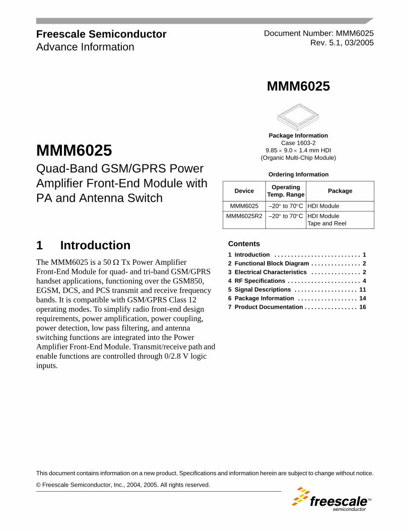
package information mmm6025 -...
TRANSCRIPT
© Freescale Semiconductor, Inc., 2004, 2005. All rights reserved.
Freescale SemiconductorAdvance Information
This document contains information on a new product. Specifications and information herein are subject to change without notice.
Document Number: MMM6025Rev. 5.1, 03/2005
MMM6025
Package InformationCase 1603-2
9.85 × 9.0 × 1.4 mm HDI(Organic Multi-Chip Module)
Ordering Information
Device Operating Temp. Range Package
MMM6025 –20° to 70°C HDI Module
MMM6025R2 –20° to 70°C HDI Module Tape and Reel
1 IntroductionThe MMM6025 is a 50 Ω Tx Power Amplifier Front-End Module for quad- and tri-band GSM/GPRS handset applications, functioning over the GSM850, EGSM, DCS, and PCS transmit and receive frequency bands. It is compatible with GSM/GPRS Class 12 operating modes. To simplify radio front-end design requirements, power amplification, power coupling, power detection, low pass filtering, and antenna switching functions are integrated into the Power Amplifier Front-End Module. Transmit/receive path and enable functions are controlled through 0/2.8 V logic inputs.
MMM6025Quad-Band GSM/GPRS Power Amplifier Front-End Module with PA and Antenna Switch
Contents1 Introduction . . . . . . . . . . . . . . . . . . . . . . . . . . 12 Functional Block Diagram . . . . . . . . . . . . . . . 23 Electrical Characteristics . . . . . . . . . . . . . . . 24 RF Specifications . . . . . . . . . . . . . . . . . . . . . . 45 Signal Descriptions . . . . . . . . . . . . . . . . . . . 116 Package Information . . . . . . . . . . . . . . . . . . 147 Product Documentation . . . . . . . . . . . . . . . . 16
MMM6025 Advance Information, Rev. 5.1
2 Freescale Semiconductor
Functional Block Diagram
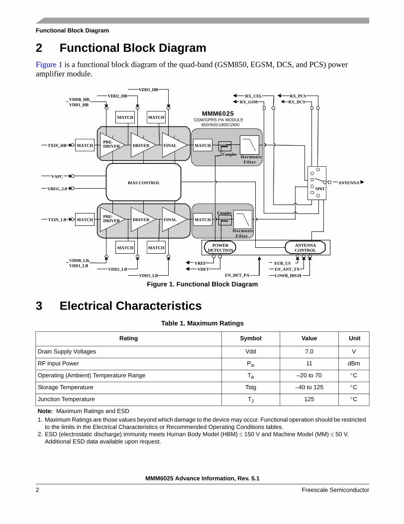
2 Functional Block DiagramFigure 1 is a functional block diagram of the quad-band (GSM850, EGSM, DCS, and PCS) power amplifier module.
Figure 1. Functional Block Diagram
3 Electrical CharacteristicsTable 1. Maximum Ratings
Rating Symbol Value Unit
Drain Supply Voltages Vdd 7.0 V
RF Input Power Pin 11 dBm
Operating (Ambient) Temperature Range TA –20 to 70 °C
Storage Temperature Tstg –40 to 125 °C
Junction Temperature TJ 125 °C
Note: Maximum Ratings and ESD1. Maximum Ratings are those values beyond which damage to the device may occur. Functional operation should be restricted
to the limits in the Electrical Characteristics or Recommended Operating Conditions tables.2. ESD (electrostatic discharge) immunity meets Human Body Model (HBM) ≤ 150 V and Machine Model (MM) ≤ 50 V.
Additional ESD data available upon request.
BIAS CONTROL
MATCH
MATCHMATCH
PRE-DRIVER DRIVER FINAL
MATCH
MATCHMATCH
PRE-DRIVER DRIVER FINAL
VDETVREF
POWERDETECTION
EN_DET
VDDB_HB,VDD1_HB
VDD3_HB
VDDB_LB,VDD1_LB
VDD3_LB
TXIN_HB
TXIN_LB
ANTENNA
MMM6025GSM/GPRS PA MODULE
850/900/1800/1900
VAPC
VREG_2.8EN_TX
VDD2_HB
VDD2_LB
RX_CELRX_GSM
RX_PCSRX_DCS
ANTENNACONTROL
EUB_US
LOWB_HIGHEN_ANT_TX
SP6T
MATCH
HarmonicFilter
Coupler
MATCHCoupler
BIAS CONTROL
MATCH
MATCHMATCH
PRE-DRIVER DRIVER FINAL
MATCH
MATCHMATCH
PRE-DRIVER DRIVER FINAL
VDETVREF
POWERDETECTION
EN_DETVDET
VREF
POWERDETECTION
EN_DET_PA
VDDB_HB,VDD1_HB
VDD3_HB
VDDB_LB,VDD1_LB
VDD3_LB
TXIN_HB
TXIN_LB
ANTENNAANTENNAVAPC
VREG_2.8
VDD2_HB
VDD2_LB
RX_CELRX_GSM
RX_CELRX_CELRX_GSMRX_GSM
RX_PCSRX_DCS
ANTENNACONTROL
EUB_US
LOWB_HIGHEN_ANT_TX
ANTENNACONTROL
EUB_US
LOWB_HIGHEN_ANT_TX
SP6TSP6T
MATCHMATCH
MATCHMATCH
HarmonicFilter

Electrical Characteristics
MMM6025 Advance Information, Rev. 5.1
Freescale Semiconductor 3
Table 2. Recommended Operating Conditions
Characteristic Symbol Min Typ Max Unit
Drain Supply Voltage Vdd 2.8 3.2 4.5 V
Power Control Ramp Voltage VRAMP 0.1 - 2.2 V
RF Input Power Pin 5 - 11 dBm
Table 3. DC Specifications
Characteristic Symbol Min Typ Max Unit
Voltage PA I (Drain Supplies)Transmitter OffTransmitter On
Vdd(TX_off)Vdd(TX_on)
-2.8
3.63.2
7.04.5
Vdc
PA Output Control Voltage VAPC 0.1 0.2 to 2.1 2.2 V
PA Output Control Current IAPC -3.0 - 3.5 mA
Detector PA Enable Voltage1
HighLow
VEN_DET_PA(H)VEN_DET_PA(L)
2.50
--
2.90.3
Vdc
Detector PA Enable Current1SourceSink
IEN_DET_PA(H)IEN_DET_PA(L)
--
--
2.010
mAµA
Mode Select VoltageUS (selects GSM850 or PCS)EU (selects EGSM or DCS)
VEUB_US(H)VEUB_US(L)
2.50
--
2.90.3
Vdc
RX Band Select CurrentSourceSink
IEUB_US(H)IEUB_US(L)
--
--
0.110
mAµA
TX Antenna Enable VoltageHighLow
VEN_ANT_TX(H)VEN_ANT_TX(L) 2.5
0--
2.90.3
Vdc
TX Antenna Enable CurrentSourceSink
IEN_ANT_TX(H)IEN_ANT_TX(L)
--
--
0.110
mAµA
Voltage PA 2 (Regulated Supply) VREG28 2.65 - 2.9 V
Current Draw IREG28 - - 18 mA
BAND SELECTHigh (DCS/PCS Bands Selected)Low (GSM850/EGSM Bands Selected)
VLOWB_HIGH(H)VLOWB_HIGH(L)
2.50
--
2.90.3
V

MMM6025 Advance Information, Rev. 5.1
4 Freescale Semiconductor
RF Specifications
The following table provides additional details on MMM6025 orderable parts.
4 RF SpecificationsThis section details specifications for the EGSM, DCS, GSM850, and PCS bands.
BAND SELECT Current LevelHighLow
ILOWB_HIGH(H)ILOWB_HIGH(L)
--
--
1010
µA
Total module leakage current (Standby condition)EN_DET_PA = 0.3 VEUB_US = EN_ANT_TX = +0.3 VLOWB_HIGH = 0.3 VVAPC = 0.1 VVREG_IN = 0 V or 2.775 V
Temp = 23 to 27°CVdd = 3.8 V
IVdd(off) - 5.0 7.0 µA
1 The MMM6025 pinout is compatible with that of MMM6022, except pin 8. MMM6025 signal EN_DET_PA (pin 16) is equivalent to a combination of both MMM6022 signals EN_TX and EN_DET.
Table 4. Orderable Parts Details
Device Operating
Temp. Range (TA)
Package RoHS Compliant Pb-Free MSLLevel SolderTemp.
MMM6025 –20° to 70°C HDI Module Yes Yes 3 250 °C
MMM6025R2 –20° to 70°C HDI Module Tape and Reel
Yes Yes 3 250 °C
Table 5. EGSM Band Specifications
Characteristic Symbol Min Typ Max Unit
EGSM BAND (Pin = 5.0 to 11 dBm, Vdd = 3.2 Vdc, VAPC = 0.1 to 2.2 V pulsed, 25% duty cycle, LOWB_HIGH = Low, EUB_US = Low, TC = 25°C ±5°C, unless otherwise noted.)
Operating FrequencyTransmitReceive
f880925
--
915960
MHz
Power Out Po(max) 33 - - dBm
Power Out Low Voltage (Vdd = 2.8 V) Po(min) 32 - - dBm
Power Added Efficiency (Saturated Pout) PAE 40 44 - %
Power Control Range1 Po(range) 35 - - dB
Power Control Slope2 ∆Vdet/∆VAPC - - 3.0 V/V
Table 3. DC Specifications (continued)
Characteristic Symbol Min Typ Max Unit
RF Specifications
MMM6025 Advance Information, Rev. 5.1
Freescale Semiconductor 5
Power Control Frequency 3.0 dB BW PC3dB 1.0 - - MHz
Power Control Response Time3 tPC - - 1.5 µs
Forward Isolation4 ISO1ISO2
--
--
-41-22
dBm
Power Detector Voltage1
Low PowerHigh Power
VDET(low)VDET(high)
401.0
--
1502.05
mVV
Harmonics5
(Pout Max = 33 dBm)2f0 – 15f0 - - -33 dBm
GSM RX Band Noise5
(Vdd = 4.2 V, Saturated Pout)(Pout = 33 dBm)
nRX(925 to 935 MHz)
- - -73 dBm/100 kHz
nRX(935 to 960 MHz)
- - -84 dBm/100 kHz
Pout over Temp (Vdd = 2.8 V, TA = -20 to 70°C) Po_ot(min) 31.5 - - dBm
Insertion Loss from Antenna to RX_GSM5 IL_RX - - 1.4 dB
Tx - Rx Isolation5
ANTENNA to RX_CELANTENNA to RX_GSMANTENNA to RX_DCSANTENNA to RX_PCS
ISO_ANT_RX_CELISO_ANT_RX_GSMISO_ANT_RX_DCSISO_ANT_RX_PCS
27272727
----
----
dB
Input VSWR VSWR - - 2:1
Power Out Change due to Coupling Variations(VSWR = 3:1 @ ANT Port)6
CPLV -1.5 - 1.5 dB
Load Mismatch Stress (Ruggedness)7 Rugg No performance degradation and no module damage
Stability - Spurious Output8 Stab - - -36 dBm
Closed Loop Power Variation over Temperature9 Pout_Temp Ambient 1(Pout = 6 dBm)
Pout_Temp Ambient 2(Pout = 20 dBm)
Pout_Temp Ambient 3(Pout = 33 dBm)
-1.5
1.0
-0.5
-
-
-
1.5
1.0
0.5
dB
dB
dB
1 Power output must be monotonic with power detector voltage. (Vdd = 2.8V to 4.5V and Temperature = -20 to +70°C)2 Vdd = 2.8V to 4.5V and Temperature = -20 to +70°C3 Measurement made from 50% of VAPC to 10%/90% of VDET_OUT final value, with pulsed VAPC with a peak voltage in the range
of 0.1 to 2.2 V and both rise and fall edges.4 Measured at antenna port, ISO1: Pin = -10 dBm, EN_ANT_TX = 0 V, VAPC = 0.1 V;
ISO2: Pin = 11 dBm, EN_ANT_TX = 2.723 V, VAPC = 0.1 V. (Vdd = 2.8V to 4.5V and Temperature = -20 to +70°C)5 Vdd = 2.8V to 4.5V and Temperature = -20 to +70°C6 Maintaining constant Vdet-Vref at all mismatch phase angles. Measured at antenna port: Pout = 33 dBm7 Output VSWR = 20:1 all phase angles, Vdd = 2.8V to 4.5V, Pin = 5dBm to 11dBm, Temperature = -20 to +70°C, Power less
than or equal to 33dBm.
Table 5. EGSM Band Specifications (continued)
Characteristic Symbol Min Typ Max Unit
MMM6025 Advance Information, Rev. 5.1
6 Freescale Semiconductor
RF Specifications
8 Output VSWR = 10:1 all phase angles, Vdd = 2.8V to 4.5V, Pin = 5dBm to 11dBm, Temperature = -20 to +70°C, Power less than or equal to 33dBm.
9 Vdiff_var = 20*LOG(Delta(T)/Delta(25°C)), where T is -20 to 65°C, Delta(T)= [Vdiff(T) with RF] - [Vdiff(T) without RF], and Delta(25°C)= [Vdiff(25°C) with RF] - [Vdiff(25°C) without RF]
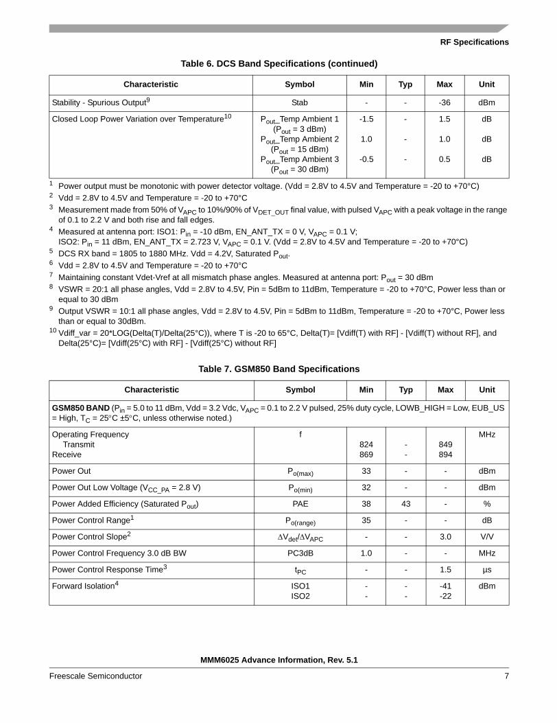
Table 6. DCS Band Specifications
Characteristic Symbol Min Typ Max Unit
DCS BAND (Pin = 5.0 to 11 dBm, Vdd = 3.2 Vdc, VAPC = 0.1 to 2.2 V pulsed, 25% duty cycle, LOWB_HIGH = High, EUB_US = Low, TC = 25°C ±5°C, unless otherwise noted.)
Operating FrequencyTransmitReceive
f17101805
--
17851880
MHz
Power Out Po(max) 30 - - dBm
Power Out Low Voltage (Vdd = 2.8 V) Po(min) 29 - - dBm
Power Added Efficiency (Saturated Pout) PAE 28 33 - %
Power Control Range1 Po(range) 35 - - dB
Power Control Slope2 ∆Vdet/∆VAPC - - 3.5 V/V
Power Control Frequency 3.0 dB BW PC3dB 1.0 - - MHz
Power Control Response Time3 tPC - - 1.5 µs
Forward Isolation4 ISO1ISO2
--
--
-53-25
dBm
Power Detector Voltage1
Low PowerHigh Power
VDET(low)VDET(high)
401.0
--
1502.05
mVV
Harmonics6
(Pout Max = 30 dBm)2f0 – 15f0 - - -33 dBm
RX Band Noise5,6
(Pout = 30 dBm)nRX - - -77 dBm/
100 kHz
Pout over Temp (Vdd = 2.8 V, TA = –20 to 70°C) Po_ot(min) 28.5 - - dBm
Insertion Loss from Antenna to RX_DCS6 IL_RX - - 1.7 dB
Tx - Rx Isolation6
ANTENNA to RX_CELANTENNA to RX_GSMANTENNA to RX_DCSANTENNA to RX_PCS
ISO_ANT_RX_CELISO_ANT_RX_GSMISO_ANT_RX_DCSISO_ANT_RX_PCS
27272727
----
----
dB
Input VSWR VSWR - - 2:1
Power Out Change due to Coupling Variations (VSWR = 3:1 @ ANT Port)7
CPLV -1.5 - 1.5 dB
Load Mismatch Stress (Ruggedness)8 Rugg No performance degradation and no module damage
RF Specifications
MMM6025 Advance Information, Rev. 5.1
Freescale Semiconductor 7
Stability - Spurious Output9 Stab - - -36 dBm
Closed Loop Power Variation over Temperature10 Pout_Temp Ambient 1 (Pout = 3 dBm)
Pout_Temp Ambient 2 (Pout = 15 dBm)
Pout_Temp Ambient 3(Pout = 30 dBm)
-1.5
1.0
-0.5
-
-
-
1.5
1.0
0.5
dB
dB
dB
1 Power output must be monotonic with power detector voltage. (Vdd = 2.8V to 4.5V and Temperature = -20 to +70°C)2 Vdd = 2.8V to 4.5V and Temperature = -20 to +70°C3 Measurement made from 50% of VAPC to 10%/90% of VDET_OUT final value, with pulsed VAPC with a peak voltage in the range
of 0.1 to 2.2 V and both rise and fall edges.4 Measured at antenna port: ISO1: Pin = -10 dBm, EN_ANT_TX = 0 V, VAPC = 0.1 V;
ISO2: Pin = 11 dBm, EN_ANT_TX = 2.723 V, VAPC = 0.1 V. (Vdd = 2.8V to 4.5V and Temperature = -20 to +70°C)5 DCS RX band = 1805 to 1880 MHz. Vdd = 4.2V, Saturated Pout.6 Vdd = 2.8V to 4.5V and Temperature = -20 to +70°C7 Maintaining constant Vdet-Vref at all mismatch phase angles. Measured at antenna port: Pout = 30 dBm8 VSWR = 20:1 all phase angles, Vdd = 2.8V to 4.5V, Pin = 5dBm to 11dBm, Temperature = -20 to +70°C, Power less than or
equal to 30 dBm 9 Output VSWR = 10:1 all phase angles, Vdd = 2.8V to 4.5V, Pin = 5dBm to 11dBm, Temperature = -20 to +70°C, Power less
than or equal to 30dBm.10 Vdiff_var = 20*LOG(Delta(T)/Delta(25°C)), where T is -20 to 65°C, Delta(T)= [Vdiff(T) with RF] - [Vdiff(T) without RF], and
Delta(25°C)= [Vdiff(25°C) with RF] - [Vdiff(25°C) without RF]
Table 7. GSM850 Band Specifications
Characteristic Symbol Min Typ Max Unit
GSM850 BAND (Pin = 5.0 to 11 dBm, Vdd = 3.2 Vdc, VAPC = 0.1 to 2.2 V pulsed, 25% duty cycle, LOWB_HIGH = Low, EUB_US = High, TC = 25°C ±5°C, unless otherwise noted.)
Operating FrequencyTransmit
Receive
f824869
--
849894
MHz
Power Out Po(max) 33 - - dBm
Power Out Low Voltage (VCC_PA = 2.8 V) Po(min) 32 - - dBm
Power Added Efficiency (Saturated Pout) PAE 38 43 - %
Power Control Range1 Po(range) 35 - - dB
Power Control Slope2 ∆Vdet/∆VAPC - - 3.0 V/V
Power Control Frequency 3.0 dB BW PC3dB 1.0 - - MHz
Power Control Response Time3 tPC - - 1.5 µs
Forward Isolation4 ISO1ISO2
--
--
-41-22
dBm
Table 6. DCS Band Specifications (continued)
Characteristic Symbol Min Typ Max Unit
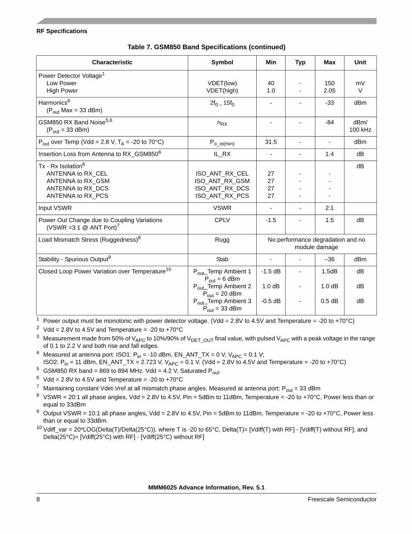
MMM6025 Advance Information, Rev. 5.1
8 Freescale Semiconductor
RF Specifications
Power Detector Voltage1
Low PowerHigh Power
VDET(low)VDET(high)
401.0
--
1502.05
mVV
Harmonics6
(Pout Max = 33 dBm)2f0 – 15f0 - - -33 dBm
GSM850 RX Band Noise5,6
(Pout = 33 dBm)nRX - - -84 dBm/
100 kHz
Pout over Temp (Vdd = 2.8 V, TA = -20 to 70°C) Po_ot(min) 31.5 - - dBm
Insertion Loss from Antenna to RX_GSM8506 IL_RX - - 1.4 dB
Tx - Rx Isolation6
ANTENNA to RX_CELANTENNA to RX_GSMANTENNA to RX_DCSANTENNA to RX_PCS
ISO_ANT_RX_CELISO_ANT_RX_GSMISO_ANT_RX_DCSISO_ANT_RX_PCS
27272727
----
----
dB
Input VSWR VSWR - - 2:1
Power Out Change due to Coupling Variations (VSWR =3:1 @ ANT Port)7
CPLV -1.5 - 1.5 dB
Load Mismatch Stress (Ruggedness)8 Rugg No performance degradation and no module damage
Stability - Spurious Output9 Stab - - –36 dBm
Closed Loop Power Variation over Temperature10 Pout_Temp Ambient 1 Pout = 6 dBm
Pout_Temp Ambient 2 Pout = 20 dBm
Pout_Temp Ambient 3 Pout = 33 dBm
-1.5 dB
1.0 dB
-0.5 dB
-
-
-
1.5dB
1.0 dB
0.5 dB
dB
dB
dB
1 Power output must be monotonic with power detector voltage. (Vdd = 2.8V to 4.5V and Temperature = -20 to +70°C)2 Vdd = 2.8V to 4.5V and Temperature = -20 to +70°C3 Measurement made from 50% of VAPC to 10%/90% of VDET_OUT final value, with pulsed VAPC with a peak voltage in the range
of 0.1 to 2.2 V and both rise and fall edges.4 Measured at antenna port: ISO1: Pin = -10 dBm, EN_ANT_TX = 0 V, VAPC = 0.1 V;
ISO2: Pin = 11 dBm, EN_ANT_TX = 2.723 V, VAPC = 0.1 V. (Vdd = 2.8V to 4.5V and Temperature = -20 to +70°C)5 GSM850 RX band = 869 to 894 MHz. Vdd = 4.2 V, Saturated Pout.6 Vdd = 2.8V to 4.5V and Temperature = -20 to +70°C7 Maintaining constant Vdet-Vref at all mismatch phase angles. Measured at antenna port: Pout = 33 dBm8 VSWR = 20:1 all phase angles, Vdd = 2.8V to 4.5V, Pin = 5dBm to 11dBm, Temperature = -20 to +70°C, Power less than or
equal to 33dBm 9 Output VSWR = 10:1 all phase angles, Vdd = 2.8V to 4.5V, Pin = 5dBm to 11dBm, Temperature = -20 to +70°C, Power less
than or equal to 33dBm.10 Vdiff_var = 20*LOG(Delta(T)/Delta(25°C)), where T is -20 to 65°C, Delta(T)= [Vdiff(T) with RF] - [Vdiff(T) without RF], and
Delta(25°C)= [Vdiff(25°C) with RF] - [Vdiff(25°C) without RF]
Table 7. GSM850 Band Specifications (continued)
Characteristic Symbol Min Typ Max Unit
RF Specifications
MMM6025 Advance Information, Rev. 5.1
Freescale Semiconductor 9
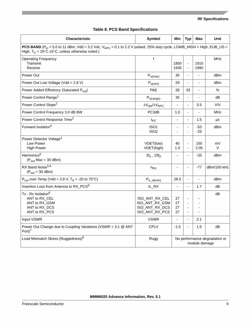
Table 8. PCS Band Specifications
Characteristic Symbol Min Typ Max Unit
PCS BAND (Pin = 5.0 to 11 dBm, Vdd = 3.2 Vdc, VAPC = 0.1 to 2.2 V pulsed, 25% duty cycle, LOWB_HIGH = High, EUB_US = High, TC = 25°C ±5°C, unless otherwise noted.)
Operating FrequencyTransmitReceive
f18501930
--
19101990
MHz
Power Out Po(max) 30 - - dBm
Power Out Low Voltage (Vdd = 2.8 V) Po(min) 29 - - dBm
Power Added Efficiency (Saturated Pout) PAE 28 33 - %
Power Control Range1 Po(range) 35 - - dB
Power Control Slope2 ∆Vdet/∆VAPC - - 3.5 V/V
Power Control Frequency 3.0 dB BW PC3dB 1.0 - - MHz
Power Control Response Time3 tPC - - 1.5 µs
Forward Isolation4 ISO1ISO2
--
--
-53-25
dBm
Power Detector Voltage1
Low PowerHigh Power
VDET(low)VDET(high)
401.0
--
1502.05
mVV
Harmonics6
(Pout Max = 30 dBm)2f0 – 15f0 - - -33 dBm
RX Band Noise5,6
(Pout = 30 dBm)nRX - - -77 dBm/100 kHz
Pout over Temp (Vdd = 2.8 V, TA = -20 to 70°C) Po_ot(min) 28.5 - - dBm
Insertion Loss from Antenna to RX_PCS6 IL_RX - - 1.7 dB
Tx - Rx Isolation6
ANT to RX_CELANT to RX_GSMANT to RX_DCSANT to RX_PCS
ISO_ANT_RX_CELISO_ANT_RX_GSMISO_ANT_RX_DCSISO_ANT_RX_PCS
27272727
----
----
dB
Input VSWR VSWR - - 2:1
Power Out Change due to Coupling Variations (VSWR = 3:1 @ ANT Port)7
CPLV -1.5 - 1.5 dB
Load Mismatch Stress (Ruggedness)8 Rugg No performance degradation or module damage
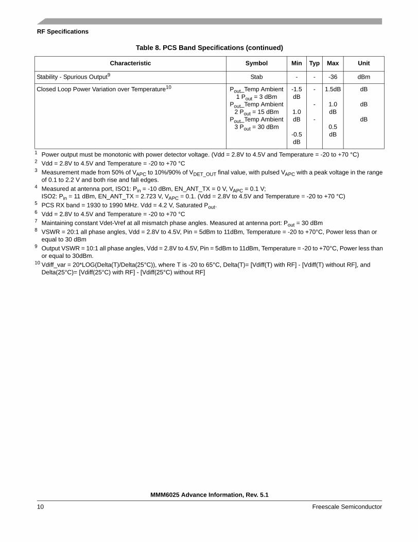
MMM6025 Advance Information, Rev. 5.1
10 Freescale Semiconductor
RF Specifications
Stability - Spurious Output9 Stab - - -36 dBm
Closed Loop Power Variation over Temperature10 Pout_Temp Ambient 1 Pout = 3 dBm
Pout_Temp Ambient 2 Pout = 15 dBm
Pout_Temp Ambient 3 Pout = 30 dBm
-1.5 dB
1.0 dB
-0.5 dB
-
-
-
1.5dB
1.0 dB
0.5 dB
dB
dB
dB
1 Power output must be monotonic with power detector voltage. (Vdd = 2.8V to 4.5V and Temperature = -20 to +70 °C)2 Vdd = 2.8V to 4.5V and Temperature = -20 to +70 °C3 Measurement made from 50% of VAPC to 10%/90% of VDET_OUT final value, with pulsed VAPC with a peak voltage in the range
of 0.1 to 2.2 V and both rise and fall edges.4 Measured at antenna port, ISO1: Pin = -10 dBm, EN_ANT_TX = 0 V, VAPC = 0.1 V;
ISO2: Pin = 11 dBm, EN_ANT_TX = 2.723 V, VAPC = 0.1. (Vdd = 2.8V to 4.5V and Temperature = -20 to +70 °C)5 PCS RX band = 1930 to 1990 MHz. Vdd = 4.2 V, Saturated Pout.6 Vdd = 2.8V to 4.5V and Temperature = -20 to +70 °C7 Maintaining constant Vdet-Vref at all mismatch phase angles. Measured at antenna port: Pout = 30 dBm8 VSWR = 20:1 all phase angles, Vdd = 2.8V to 4.5V, Pin = 5dBm to 11dBm, Temperature = -20 to +70°C, Power less than or
equal to 30 dBm 9 Output VSWR = 10:1 all phase angles, Vdd = 2.8V to 4.5V, Pin = 5dBm to 11dBm, Temperature = -20 to +70°C, Power less than
or equal to 30dBm.10 Vdiff_var = 20*LOG(Delta(T)/Delta(25°C)), where T is -20 to 65°C, Delta(T)= [Vdiff(T) with RF] - [Vdiff(T) without RF], and
Delta(25°C)= [Vdiff(25°C) with RF] - [Vdiff(25°C) without RF]
Table 8. PCS Band Specifications (continued)
Characteristic Symbol Min Typ Max Unit

Signal Descriptions
MMM6025 Advance Information, Rev. 5.1
Freescale Semiconductor 11
5 Signal Descriptions
Figure 2. Pin Out
Table 9. Contact Connections
Section Signal Description Pin(s)
RF TXIN_LB TX Input (Low Bands), DC Blocked 6
TXIN_HB TX Input (High Bands), DC Blocked 4
ANT Antenna 21
RX_GSM RX Output (GSM Band) 23
RX_DCS RX Output (DCS Band) 27
RX_CEL RX Output (CEL Band) 25
RX_PCS RX Output (PCS Band) 29
VD
D3_
HB
VAPC
TXIN_HB
TXIN_LB
VR
EG
28
ANT
Gnd
EN
_DE
T_PA
VR
EF
VD
ET
Gnd
EN_ANT_TX
Gnd
LO
WB
_HIG
H
Gnd
NC
Gnd
Gnd
EUB_US
GndG
nd
VD
D3_
LB
RX
_DC
S
RX
_PC
S
RX_GSM
RX_CEL
Gnd
VD
DB_
HB
+V
DD
1_H
B
1613 151410 11 12 17
25
21
19
23
18
26293034 33 32 27
2
6
8
4
9
1
MMM6025(Top View Through Package)
9.85 mm × 9.0 mm(± 0.1 mm)
3
7
5
31 28
24
20
22
VD
D2_
HB
VD
D2_
LB
VD
DB
_LB
+ V
DD
1_L
B
Gnd
Gnd
Gnd
MMM6025 Advance Information, Rev. 5.1
12 Freescale Semiconductor
Signal Descriptions
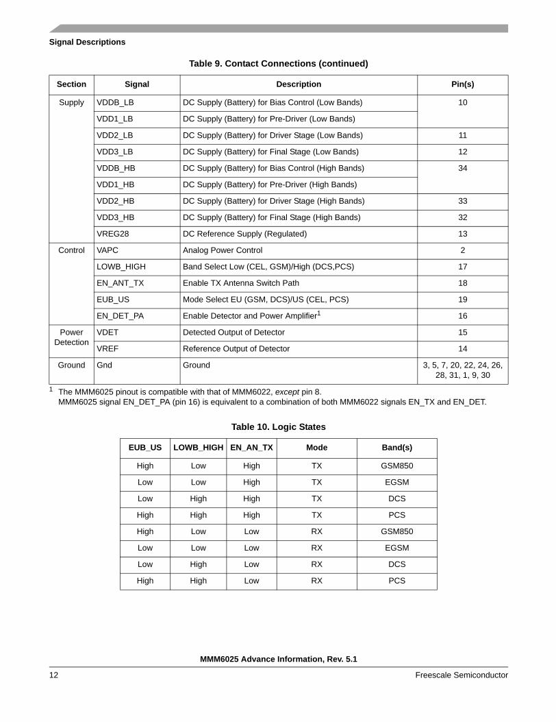
Supply VDDB_LB DC Supply (Battery) for Bias Control (Low Bands) 10
VDD1_LB DC Supply (Battery) for Pre-Driver (Low Bands)
VDD2_LB DC Supply (Battery) for Driver Stage (Low Bands) 11
VDD3_LB DC Supply (Battery) for Final Stage (Low Bands) 12
VDDB_HB DC Supply (Battery) for Bias Control (High Bands) 34
VDD1_HB DC Supply (Battery) for Pre-Driver (High Bands)
VDD2_HB DC Supply (Battery) for Driver Stage (High Bands) 33
VDD3_HB DC Supply (Battery) for Final Stage (High Bands) 32
VREG28 DC Reference Supply (Regulated) 13
Control VAPC Analog Power Control 2
LOWB_HIGH Band Select Low (CEL, GSM)/High (DCS,PCS) 17
EN_ANT_TX Enable TX Antenna Switch Path 18
EUB_US Mode Select EU (GSM, DCS)/US (CEL, PCS) 19
EN_DET_PA Enable Detector and Power Amplifier1 16
Power Detection
VDET Detected Output of Detector 15
VREF Reference Output of Detector 14
Ground Gnd Ground 3, 5, 7, 20, 22, 24, 26, 28, 31, 1, 9, 30
1 The MMM6025 pinout is compatible with that of MMM6022, except pin 8.MMM6025 signal EN_DET_PA (pin 16) is equivalent to a combination of both MMM6022 signals EN_TX and EN_DET.
Table 10. Logic States
EUB_US LOWB_HIGH EN_AN_TX Mode Band(s)
High Low High TX GSM850
Low Low High TX EGSM
Low High High TX DCS
High High High TX PCS
High Low Low RX GSM850
Low Low Low RX EGSM
Low High Low RX DCS
High High Low RX PCS
Table 9. Contact Connections (continued)
Section Signal Description Pin(s)
Signal Descriptions
MMM6025 Advance Information, Rev. 5.1
Freescale Semiconductor 13
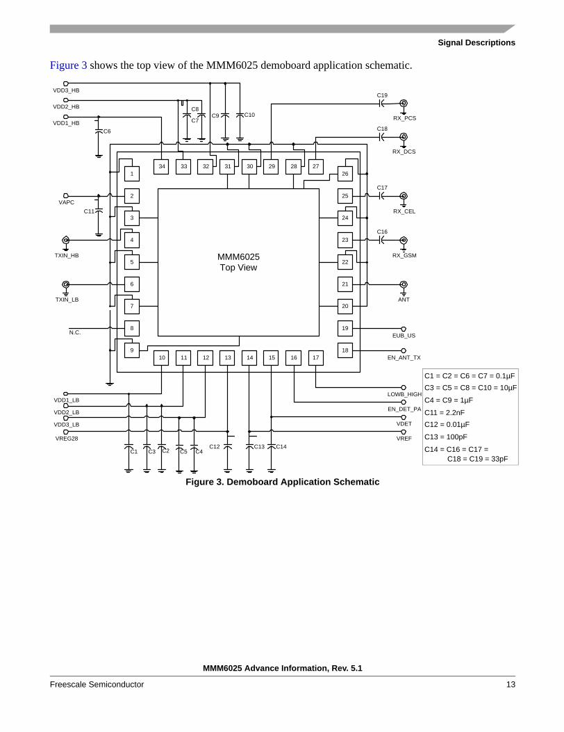
Figure 3 shows the top view of the MMM6025 demoboard application schematic.
Figure 3. Demoboard Application Schematic
1
2
3
4
5
6
7
8
9
26
25
24
23
22
21
20
19
18
2728293031323334
1716151413121110
C16
C17
C18
C19
ANT
EUB_US
EN_ANT_TX
LOWB_HIGH
EN_DET_PA
VDET
VREFC14C13
TXIN_LB
TXIN_HB
VDD2_LB
VREG28C12
C2C3
N.C.
C11VAPC
VDD1_HBC6
MMM6025Top View
VDD2_HB
VDD3_HB
C10C9C8
C7
C4C5
VDD3_LB
VDD1_LB
C1
RX_GSM
RX_DCS
RX_PCS
RX_CEL
C1 = C2 = C6 = C7 = 0.1µFC3 = C5 = C8 = C10 = 10µF
C4 = C9 = 1µF
C11 = 2.2nFC12 = 0.01µF
C13 = 100pF
C14 = C16 = C17 =C18 = C19 = 33pF
MMM6025 Advance Information, Rev. 5.1
14 Freescale Semiconductor
Package Information
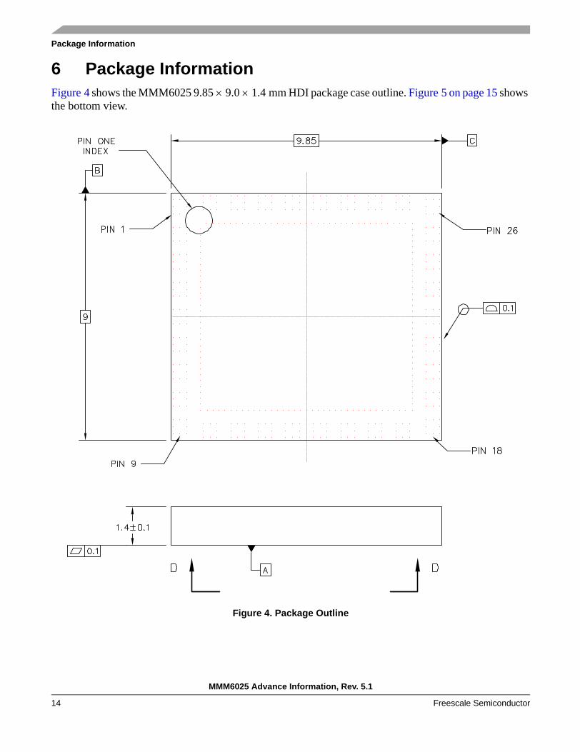
6 Package InformationFigure 4 shows the MMM6025 9.85 × 9.0 × 1.4 mm HDI package case outline. Figure 5 on page 15 shows the bottom view.
Figure 4. Package Outline

Package Information
MMM6025 Advance Information, Rev. 5.1
Freescale Semiconductor 15
Figure 5. Package Outline—Bottom View
Document Number: MMM6025Rev. 5.103/2005
How to Reach Us:
Home Page:www.freescale.com
E-mail:[email protected]
USA/Europe or Locations Not Listed:Freescale SemiconductorTechnical Information Center, CH3701300 N. Alma School RoadChandler, Arizona 85224+1-800-521-6274 or [email protected]
Europe, Middle East, and Africa:Freescale Halbleiter Deutschland GmbHTechnical Information CenterSchatzbogen 781829 Muenchen, Germany+44 1296 380 456 (English)+46 8 52200080 (English)+49 89 92103 559 (German)+33 1 69 35 48 48 (French)[email protected]
Japan:Freescale Semiconductor Japan Ltd.HeadquartersARCO Tower 15F1-8-1, Shimo-Meguro, Meguro-ku,Tokyo 153-0064, Japan0120 191014 or +81 3 5437 [email protected]
Asia/Pacific:Freescale Semiconductor Hong Kong Ltd.Technical Information Center2 Dai King StreetTai Po Industrial EstateTai Po, N.T., Hong Kong+800 2666 [email protected]
For Literature Requests Only:Freescale Semiconductor Literature Distribution CenterP.O. Box 5405Denver, Colorado 802171-800-521-6274 or 303-675-2140Fax: [email protected]
Information in this document is provided solely to enable system and software implementers to use Freescale Semiconductor products. There are no express or implied copyright licenses granted hereunder to design or fabricate any integrated circuits or integrated circuits based on the information in this document.Freescale Semiconductor reserves the right to make changes without further notice to any products herein. Freescale Semiconductor makes no warranty, representation or guarantee regarding the suitability of its products for any particular purpose, nor does Freescale Semiconductor assume any liability arising out of the application or use of any product or circuit, and specifically disclaims any and all liability, including without limitation consequential or incidental damages. “Typical” parameters that may be provided in Freescale Semiconductor data sheets and/or specifications can and do vary in different applications and actual performance may vary over time. All operating parameters, including “Typicals”, must be validated for each customer application by customer’s technical experts. Freescale Semiconductor does not convey any license under its patent rights nor the rights of others. Freescale Semiconductor products are not designed, intended, or authorized for use as components in systems intended for surgical implant into the body, or other applications intended to support or sustain life, or for any other application in which the failure of the Freescale Semiconductor product could create a situation where personal injury or death may occur. Should Buyer purchase or use Freescale Semiconductor products for any such unintended or unauthorized application, Buyer shall indemnify and hold Freescale Semiconductor and its officers, employees, subsidiaries, affiliates, and distributors harmless against all claims, costs, damages, and expenses, and reasonable attorney fees arising out of, directly or indirectly, any claim of personal injury or death associated with such unintended or unauthorized use, even if such claim alleges that Freescale Semiconductor was negligent regarding the design or manufacture of the part.
Freescale™ and the Freescale logo are trademarks of Freescale Semiconductor, Inc. All other product or service names are the property of their respective owners.
© Freescale Semiconductor, Inc. 2004, 2005. All rights reserved.
7 Product DocumentationThis data sheet is labeled as a particular type: Product Preview, Advance Information, or Technical Data. Definitions of these types are available at: http://www.freescale.com on the documentation page.
Table 11 summarizes revisions to this document since the previous release (Rev. 5).Table 11. Revision History
Location Revision
Mulitple locations Changed Case Temp to Ambient Temp. Added Tape and Reel and Lead Free information.