paper special section on heterostructure … special section on heterostructure microelectronics...
TRANSCRIPT

1238IEICE TRANS. ELECTRON., VOL.E93–C, NO.8 AUGUST 2010
PAPER Special Section on Heterostructure Microelectronics with TWHM 2009
Efficient AlGaN/GaN Linear and Digital-Switch-Mode PowerAmplifiers for Operation at 2 GHz∗
Stephan MAROLDT†, Dirk WIEGNER††, Stanislav VITANOV†††, Vassil PALANKOVSKI†††, Nonmembers,Rüdiger QUAY†a), Member, and Oliver AMBACHER†, Nonmember
SUMMARY This work addresses the enormous efficiency and linear-ity potential of optimized AlGaN/GaN high-electron mobility transistors(HEMT) in conventional Doherty linear base-station amplifiers at 2.7 GHz.Supported by physical device simulation, the work further elaborates onthe use of AlGaN/GaN HEMTs in high-speed current-switch-mode class-D (CMCD)/class-S MMICs for data rates of up to 8 Gbit/s equivalent to2 GHz RF-operation. The device needs for switch-mode operation are de-rived and verified by MMIC results in class-S and class-D operation. To theauthors’ knowledge, this is the first time 2 GHz-equivalent digital-switch-mode RF-operation is demonstrated with GaN HEMTs with high efficiency.key words: Gallium Nitride, power amplifier, switch-mode, efficiency
1. Introduction
Energy harvesting is a key issue in the development of greeninformation and communication technology. Energy effi-ciency is further a vital prerequisite in order to make useof the astounding electrical RF-power potential of groupIII-Nitride semiconductor devices in real communicationsystems [1]. III-Nitride high-electron mobility transistors(HEMTs) enable new amplifier concepts at RF-frequenciesbased on their increased device speed and ruggedness andthe unique combination of speed and high breakdown volt-age. Very high efficiency values can be achieved with con-ventional linearized Doherty amplifiers, as shown in thiswork. In addition, new III-N amplifier can be part of moreadvanced transceiver concepts, as depicted in Fig. 1. Theaim of this work is to harvest efficiency and to reduce com-ponent usage in the chain from the digital output-I/Q of anycommunication system. The schematic of the transceiverchain in a base station is given in Fig. 1. The potential ad-vantage of using switch-mode amplifiers is a more efficientorganization from the I/Q-output of the digital signal pro-cessing (DSP) to the analog antenna output. The early D/A-conversion can be avoided and the digital signal is main-tained up to the power amplifier potentially allowing for in-creased efficiency.
Manuscript received November 21, 2009.Manuscript revised March 31, 2010.†The authors are with the Fraunhofer Institute Applied Solid-
State Physics, Tullastr. 72, D-79108 Freiburg, Germany.††The author is with Alcatel-Lucent Bell Labs Germany Radio
Communications-Dept. ZFZ/RA4, Germany.†††The authors are with the Advanced Materials and De-
vice Analysis Group, Inst. for Microelectronics, TU Wien,Gusshausstr. 27–29, 1040 Wien, Austria.
∗This paper was partially presented at the TWHM 2009.a) E-mail: [email protected]
DOI: 10.1587/transele.E93.C.1238
Fig. 1 Concepts of transceiver chains.
2. Device Technology and Simulation
Gallium Nitride HEMTs provide the outstanding propertiesof high-breakdown voltage in combination with the capabil-ity of very fast switching. Derived from an optimized analogpower bar process, three process variants were used for theinvestigation of advanced broadband switching with the aimto reach 2 GHz operation.
2.1 Epitaxy and Technology
The epitaxial structures used in this work were grown bymetal-organic chemical vapor deposition (MOCVD) on 3-inch semi-insulating SiC substrates. The layers consistof a highly-resistive c-plane GaN buffer, followed by anAl0.22Ga0.78N barrier and finally a thin GaN cap layer. Roomtemperature Hall measurements on the two-dimensionalelectron gas (2DEG) formed at the buffer to barrier inter-face resulted in a sheet resistance, a sheet carrier concen-tration, and a mobility of 500Ω/sq, 8 × 1012 cm−2, and1600 cm2/(Vs), respectively. After epitaxial growth, ohmiccontacts were formed, showing a low contact resistance of0.2Ωmm [3]. The nitride-assisted T-gate was used withthree different gate lengths of 0.5 µm, 0.25 µm, and 0.15 µm,and was defined by e-beam lithography and trench etchinginto the SiN passivation [2]. Table 1 gives an overviewon performance parameters of the three process variants in-vestigated in this paper. The comparison is performed onthe same epitaxy, while contact spacings and pitches arematched to the needs of the individual process nodes. Re-sults on the powerbar capabilities of the process with a gate
Copyright c© 2010 The Institute of Electronics, Information and Communication Engineers
MAROLDT et al.: EFFICIENT ALGAN/GAN LINEAR AND DIGITAL-SWITCH-MODE POWER AMPLIFIERS FOR OPERATION AT 2 GHZ1239
Table 1 Some analog features of the AlGaN/GaN device technologiesapplied.
Gate length [µm] 0.5 0.25 0.15Operation bias [V] 50 28 20
BVGD [V] 160 100 20fT [GHz] 15 32 50
PAE % 65 55 29@ frequency [GHz] 2 10 27
length of 0.5µm have been reported elsewhere, e.g., [2]. Inanalog class-A-B operation, the process yields a very highPAE of up to 65%, as given in Table 1. Reasonably-highanalog efficiency figures are given for two other gate lengthsfor higher frequencies of 10 GHz and 27 GHz for reference.
Furthermore the coplanar MMIC-process includesNiCr based 50Ω/sq thin film resistors, metal-insulator-metal(MIM) capacitors as well as a thick plated Au-based airbridge technology.
2.2 Device Simulation of Switch-Mode HEMTs
To clarify the needs for switch-mode operation, theAlGaN/GaN devices are analyzed by means of two-dimensional hydrodynamic simulations using Minimos-NT,which was successfully employed for the development ofAlGaN/GaN HEMTs [4], [5]. Material properties, such asband energies, carrier mobilities, and carrier energy relax-ation times are properly modeled. The densities of the po-larization charges at the channel/barrier interface and at thebarrier/cap interface are determined by calibration againstthe experimental data to be 9×1012 cm−2 and −2×1012 cm−2,respectively. Self-heating effects are accounted for by usingsubstrate thermal contact in the simulation.
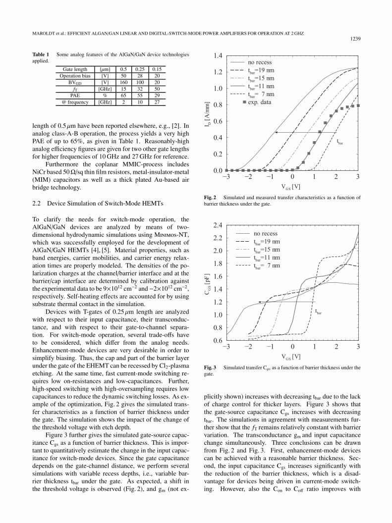
Devices with T-gates of 0.25 µm length are analyzedwith respect to their input capacitance, their transconduc-tance, and with respect to their gate-to-channel separa-tion. For switch-mode operation, several trade-offs haveto be considered, which differ from the analog needs.Enhancement-mode devices are very desirable in order tosimplify biasing. Thus, the cap and part of the barrier layerunder the gate of the EHEMT can be recessed by Cl2-plasmaetching. At the same time, fast current-mode switching re-quires low on-resistances and low-capacitances. Further,high-speed switching with high-oversampling requires lowcapacitances to reduce the dynamic switching losses. As ex-ample of the optimization, Fig. 2 gives the simulated trans-fer characteristics as a function of barrier thickness underthe gate. The simulation shows the impact of the change ofthe threshold voltage with etch depth.
Figure 3 further gives the simulated gate-source capac-itance Cgs as a function of barrier thickness. This is impor-tant to quantitatively estimate the change in the input capac-itance for switch-mode devices. Since the gate capacitancedepends on the gate-channel distance, we perform severalsimulations with variable recess depths, i.e., variable bar-rier thickness tbar under the gate. As expected, a shift inthe threshold voltage is observed (Fig. 2), and gm (not ex-
Fig. 2 Simulated and measured transfer characteristics as a function ofbarrier thickness under the gate.
Fig. 3 Simulated transfer Cgs as a function of barrier thickness under thegate.
plicitly shown) increases with decreasing tbar due to the lackof charge control for thicker layers. Figure 3 shows thatthe gate-source capacitance Cgs increases with decreasingtbar. The simulations in agreement with measurements fur-ther show that the fT remains relatively constant with barriervariation. The transconductance gm and input capacitancechange simultaneously. Three conclusions can be drawnfrom Fig. 2 and Fig. 3. First, enhancement-mode devicescan be achieved with a reasonable barrier thickness. Sec-ond, the input capacitance Cgs increases significantly withthe reduction of the barrier thickness, which is a disad-vantage for devices being driven in current-mode switch-ing. However, also the Con to Coff ratio improves with

1240IEICE TRANS. ELECTRON., VOL.E93–C, NO.8 AUGUST 2010
reduced barrier thickness. Third, as the transconductancealso increase accordingly, the current-drive capability of theswitch-mode FETs improves. Overall, moving the thresh-old voltage closer to 0 V improves the switching capabili-ties even without actually reaching enhancement-mode op-eration. For a given cut-off frequency, it is further desirableto have a high transconductance in order to improve the ca-pability to drive parasitic lines in a current-mode amplifier.Last, reduction of the on-resistance Ron is key to minimizeohmic switching losses while maintaining reasonable de-vice pinch-off at high-bias. In this study this is achieved byproper scaling of the contact separations for reduced gate-lengths accordingly.
3. GaN Doherty Amplifiers
Still based on silicon LDMOS and conventional GaNdepletion-mode HEMTs, Doherty amplifiers are theworkhorse of ourdays base-station replacing more conven-tional class-A-B amplifiers for linear efficiency reasons [6].To that end a symmetric Doherty amplifier based on GaNHEMTs was realized and was linearized under realistic basestation conditions. The fundamental gate periphery of theamplifier is Wg = 2 × 32 mm. The AlGaN/GaN HEMTs isbased on a gate length of 0.5 µm in this case with a thresh-old voltage of −3 V. The baseline technology refers to thenon-recessed version in Fig. 2. The powerbar devices arepackaged in conventional ceramic packages. The image ofthe complete amplifier is given in Fig. 4. The devices are bi-ased at VDS = 30 V. The peak amplifier was biased in class-CVGS = −4 V, while the carrier amplifier was biased in class-A-B equivalent to a quiescent current of ID,q = 100 mA/mm.At a high frequency of 2.7 GHz a small-signal gain of 9 dBis obtained.
One-carrier W-CDMA performance with digital pre-distorsion (DPD) and clipping reaches an average outputpower of 44.9 dBm (30.9 W) and a peak power of 50.5 dBm(112 W) at 2.7 GHz. The linearized spectrum at 2.7 GHz is
Fig. 4 Image of the symmetric GaN Doherty amplifier.
given in Fig. 5. The markers for the 5 MHz and 10 MHz off-set from the carrier are indicated. The measured associateddrain efficiency (DE) of the linearized operation is >45%at 2.7 GHz and the 3GPP-ACLR specifications are met with−47 dB at 5 MHz and with −55 dB at 10 MHz offset. Thisexample shows the excellent potential of conventional GaNFETs under realistic operating conditions up to a high fre-quency of 2.7 GHz with excellent linear PAE.
4. Switch-Mode Core MMICs
More advanced amplifier concepts such as class-S ampli-fiers have been suggested, e.g., in [7], however, operatingat 450 MHz only. It is the aim of this work to demonstrateswitch-mode core chips for data rates of >5 Gbits/s equiva-lent to 2.14 GHz operation, i.e., realistic mobile communi-cation frequencies. Some aspects of circuit design of corechips based on a gate length of 0.25 µm were reported in[8]. For reference, the schematic is given in Fig. 6. The in-
Fig. 5 Output power spectrum of the GaN Doherty amplifier at 2.7 GHz.
Fig. 6 Schematic of the dual-stage source follower core chip.

MAROLDT et al.: EFFICIENT ALGAN/GAN LINEAR AND DIGITAL-SWITCH-MODE POWER AMPLIFIERS FOR OPERATION AT 2 GHZ1241
Fig. 7 Micrograph of a CMCD MMIC, chip size 2 mm × 2 mm.
put stage of the driver is biased externally. The output stageis biased with the DC-VDS. The major application of suchan MMIC PA is either a current-mode class-S operation ora current-mode class-D operation. In the experiment for es-timating the class-D or class-S operation a square wave in-put signal (class-D) or a BPDS modulated signal (class-S)were applied to a dual-stage common source amplificationcircuit. The gate of the driver is biased at a typical DC-biasin class-A (VGS = −1.3 V), which is adjusted via an externalbias-Tee and the the two bias VTpos and VTneg .
Figure 7 gives the micrograph of a broadband ampli-fier core chip in differential configuration investigated forvarious gate technologies in the following. For class-S op-eration band pass delta-sigma (BPDS) modulated signals re-quest a very high signal bandwidth, which is the reason forapplying a technology with a gate length as low as 0.15 µm.The frequency spectrum of the BPDS signal is defined fromnearly DC to at least 4th harmonic due to a four times sig-nal oversampling in generating the BPDS signal. A typicalspectrum in class-S operation is given in Fig. 8 for a datarate of 5.2 Gbit/s. The main areas of interest include the lossmechanisms at high-data rates and the dependence of PAEand output power as a function of bias.
4.1 MMIC Circuit Design and Broadband Measurements
Circuit simulation and design were carried out using Agi-lent’s ADS simulation environment including our in-housedeveloped GaN HEMT large signal model. Because of thevery high signal bandwidth of the modulated input signal,no conventional matching circuit can be applied to the in-put/output of the MMIC. Thus, the particular amplifiers canbe operated at any bitrate within their particular bandwidth
Fig. 8 Output spectrum under class-S operation for 5.2 Gbit/s.
determined mainly by the active device technology. Circuitdesign consist of waveform shaping for the particular maxi-mum bitrate of the individual MMIC.
Broadband measurements were performed on a high-bandwidth (50 kHz to 40 GHz) measurement setup. Theinput signal source consists of an Anritsu MP1758A pat-tern generator with a series-connected preamplifier. Ahigh power attenuator was used as broadband 50Ω out-put load. The input and output bias networks were chosenvery carefully to preserve the minimum and maximum avail-able frequency of the measurement setup. A 50 GHz Ag-ilent sampling scope (86100 with 83484A) combined witha software-based spectral S-parameter correction was uti-lized for broadband measurements of the waveforms. Alldata given in the following refer to measured broadband sig-nals without any filtering, which, however, has to be appliedfor proper class-D/S operation in the final amplifier mod-ule. The measurements were taken for one amplifier of thedifferential amplifier pair shown in Fig. 7. For a full differ-ential amplifier including a filter, a doubling in output powerwith nearly no decrease in efficiency is expected, as evalu-ated by circuit simulations. As an example for the signals,Fig. 9 gives the time-domain measurements at 0.9 Gbit/s,and 4 Gbit/s, respectively, for a core chip with a gate lengthof 0.15 µm.
4.2 Core Chip Realization
Power amplifier core-chip CMCD-MMICs based on GaNHEMTs with gate lengths of 0.5 µm, 0.25 µm, and 0.15 µmusing advanced III-N MMIC processes are compared in thiswork. The CMCD-MMICs are designed in a dual-stageconfiguration with a gate width of 2 × 1.2 mm (for all gatelengths). The stages are mirrored for differential operation,as shown in Fig. 7.
4.3 Digital Class-D Operation
The class-D operation is induced by a periodic square waveinput signal. The measured output bit-sequence at a data rateof 0.9 and 4 Gbit/s in square-wave operation was already

1242IEICE TRANS. ELECTRON., VOL.E93–C, NO.8 AUGUST 2010
Fig. 9 Time domain measurements in current-mode class-D operation at0.9 Gbit/s and 4 Gbit/s at an operation bias VDS = 15 V.
Fig. 10 Output and PAE power vs. bitrate in class-D operation.
given in Fig. 9 for a device with a gate length of 0.15 µm. Weobserve a voltage swing of 28 V at a DC-bias of VDS = 15 V.The dependence of the switch-mode output power, broad-band drain efficiency (DE), and broadband power-added ef-ficiency (PAE) on bit rate in square-wave class-D operationis given in Fig. 10 for half of the circuit shown in Fig. 7.We use a calibrated and frequency corrected spectrum ana-lyzer as a receiver for the broadband signal between near DCand 18 GHz. The passive losses in the set-up are accountedfor likewise. The efficiency quantities drain efficiency (DE)and power-added efficiency (PAE) are calculated from thetotal broadband output and input power and the DC-power.The figure yields a maximum PAE of 74% at 0.9 Gbit/s and53% at 4 Gbit/s. The output power level reaches 3–3.5 Wfor a gate width of 1.2 mm, which is equivalent to an out-put power density of up to 2.9 W/mm at VDS = 15 V. For agiven bias, the impact of the dynamic switching losses forthis high-bit rate operation can be deduced from this figure.
Figure 11 gives the dependence of output power andPAE as a function of operation bias at 900 MHz in class-Doperation, again for a gate length of 0.15 µm. An increaseof the output power to 5 W is observed when increasing theoperation bias, and likewise, the maximum voltage swingof the switch. The efficiency drops for two reasons: first,
Fig. 11 Output power and PAE vs. DC-voltage VDSat 900 MHz(1.8 Gbit/s) in class-D operation.
Fig. 12 Output and PAE power vs. bitrate in class-S operation for VDS =
15 V.
the design is optimized with respect to the reduction of theswitching losses at a particular operation bias; second, and abit more subtle: although the broadband device is not reallymatched to 50Ω load in an analog microwave sense, how-ever, when increasing the operation bias, the average mis-match of the HEMT impedance over frequency moves awayfrom the 50Ω load offered by the output line, which reducesPAE.
4.4 Digital Class-S Operation
For class-S operation a numerical generated 128k BPDS bitstream related to a 1-tone carrier at the specific fundamentalfrequency is used for the input signal. Figure 12 gives outputpower and PAE vs. bitrate for a MMIC, again with a gatelength of 0.15 µm, measured up to 8 Gbit/s.
In this case for the same bit rate the PAE values arehigher than in class-D and reach 63% at 5 Gbit/s. This canexplained by the pulse-length modulation of the class-S sig-nal, which has lower and higher frequency contributions, sothat the devices are not always operated at the critical maxi-mum of the frequency range.

MAROLDT et al.: EFFICIENT ALGAN/GAN LINEAR AND DIGITAL-SWITCH-MODE POWER AMPLIFIERS FOR OPERATION AT 2 GHZ1243
Table 2 MMIC comparison in class-D operation at 900 MHz(1.8 Gbit/s).
lg [µm] 0.5 0.25 0.15
Wg [mm] 1.2 1.2 1.2
VDS
20 V PAE (DE) 59% (67%) 62% (69%) 68% (74%)20 V Pout 4.0 W 4.3 W 5.1 W15 V PAE (DE) 59% (71%) 62% (73%) 67% (77%)15 V Pout 2.7 W 2.8 W 3.2 W
Table 3 MMIC comparison in class-D operation at 450 MHz(0.9 Gbit/s).
lg 0.5 µm 0.5 µm
Wg 2 mm 1.2 mm
VDS
20 V PAE (DE) 70% (79%) 69% (76%)20 V Pout 6.0 W 4.9 W15 V PAE (DE) 66% (80%) 67% (80%)15 V Pout 3.6 W 3.1 W
5. MMIC Technology Comparison at 900 MHz(1.8 Gbit/s)
Among the MMICs discussed in the last section, a system-atic comparison is performed including all three gate pro-cesses. Table 2 compares CMCD-MMICs in class-D oper-ation for a data rate of 900 MHz. Several trends typical forswitch-mode operation are observed: for a given bias anddata rate the efficiency and output power increase with re-duced gate lengths due to the improvement of the switchinglosses and the reduction of of the on-resistance. In this com-parison, 900 MHz is the highest frequency for which mea-surements for all three gate lengths can be taken, particu-larly with respect to the gate lengths of 0.5 µm. One gen-eral limitation of the power measurements is the voltage andpower limitation of the broadband bias-tees (up to 40 GHz),which are limited to 5 W and 20 V, thus measurements be-yond these values are not taken.
Larger gate widths allow switching of higher currentsand thus increased output power levels. However, largergate widths also mean a reduction in speed and thus effi-ciency for a given data rate. Table 3 gives the comparison oftwo MMICs with the same gate length of 0.5 µm in class-Doperation at 450 MHz. In this case the speed of the deviceis sufficient and only then the output power increases withgate width for nearly identical PAE and DE values.
6. Conclusions
In summary, this works demonstrates the enormous poten-tial in efficiency and linearity potential of optimized Al-GaN/GaN HEMTs in both conventional linear and switch-mode applications. Based on device simulations, the dif-ferent requirements of AlGaN/GaN HEMTs for the switch-mode operation become visible, where threshold voltage,R on-reduction, and capacitance reduction are dominant and
have a direct impact on PAE and DE of the RF-power ampli-fier. Further, GaN Doherty base-station amplifiers demon-strate the enormous linearity potential at high operation fre-quencies of 2.7 GHz.
The use of AlGaN/GaN HEMTs in high-speed current-mode class-D/class-S MMICs for data rates of up to 8 Gbit/sin switch-mode operation equivalent to 2 GHz RF-operationshows the potential of GaN processes scaled to gate lengthof 0.15 µm for current-mode switching and the related effi-ciency vs. bitrate trade-offs. Very high switching efficien-cies are reached for data rates as high as 8 Gbit/s, whilethe relative drop in PAE and DE suggests further reductionof the on-resistance and the parasitic capacitances for high-efficiency operation
Acknowledgments
The authors acknowledge the support of the German min-istry of education and research in the project class-S andELBA. The authors further acknowledge support from theAustrian Science Fund (FWF) and BMWF, Project STARTY247-N13.
References
[1] R. Quay, F. van Raay, J. Kühn, R. Kiefer, P. Waltereit, M. Zorcic,M. Musser, W. Bronner, M. Dammann, M. Seelmann-Eggebert, M.Schlechtweg, M. Mikulla, O. Ambacher, J. Thorpe, K. Riepe, F.van Rijs, M. Saad, L. Harm, and T. Rödle, “Efficient AlGaN/GaNHEMT power amplifiers,” Proc. European Microwave Integrated Cir-cuits Conference (EUMIC) 2008, pp.87–90, Amsterdam, 2008.
[2] P. Waltereit, W. Bronner, R. Quay, M. Dammann, S. Müller, R.Kiefer, B. Raynor, M. Mikulla, and G. Weimann, “High-efficiencyGaN HEMTs on 3-inch semi-insulating SiC substrates,” Physica Sta-tus Solidi A, vol.205, pp.1078–1080, May 2008.
[3] S. Maroldt, C. Haupt, W. Pletschen, S. Mueller, R. Quay, O.Ambacher, C. Schippel, and F. Schwierz, “Gate-Recessed Al-GaN/GaN based enhancement-mode high electron mobility transis-tors for high frequency operation,” Jpn. J. Appl. Phys., vol.48, no.4,04C083(3), 2009.
[4] S. Vitanov, V. Palankovski, S. Murad, T. Roedle, R. Quay, and S.Selberherr, “Predictive simulation of AlGaN/GaN HEMTs,” Tech.Dig. IEEE CSIC Symp., pp.131–134, 2007.
[5] S. Vitanov, V. Palankovski, S. Murad, T. Roedle, R. Quay, andS. Selberherr, “Hydrodynamic modeling of AlGaN/GaN HEMTs,”Simulation of Semiconductor Processes and Devices, pp.273–276,Springer, Wien, New York, 2007.
[6] C. Cassan, J. Jones, and O. Lembeye, “A 2-stage 150 W 2.2 GHz dualpath LDMOS RF power amplifier for high efficiency applications,”Internaiotnal Microwave Symp. (IMS), pp.655–658, Atlanta, 2008.
[7] C. Meliani, J. Flucke, A. Wentzel, J. Würfl, W. Heinrich, and G.Tränkle, “Switch-mode amplifier ICs with over 90% efficiency forclass-S PAs using GaAs-HBTs and GaN-HEMTs,” International Mi-crowave Symp. (IMS), pp.751–754, Atlanta, 2008.
[8] S. Maroldt, C. Haupt, R. Kiefer, W. Bronner, S. Müller, W. Benz,R. Quay, and O. Ambacher, “High efficiency digital GaN MMICpower amplifiers for future switch-mode based mobile communica-tion systems,” Compound Semiconductor Integrated Circuit Sympo-sium, pp.73–76, 2009.

1244IEICE TRANS. ELECTRON., VOL.E93–C, NO.8 AUGUST 2010
Stephan Maroldt received the Dipl.-Ing.degree in electrical engineering, with emphasison microelectronics, from Technical UniversityIlmenau, Germany, in 2006. After graduationhe has began working on his Ph.D. degree inthe nanotechnology group at the Technical Uni-versity Ilmenau in the field of GaN HFET tech-nology. Since 2008 he is with Fraunhofer In-stitute of Applied Solid-State Physics where hehas continued working towards the Ph.D. de-gree. His mayor field of research is the design
and technology for GaN HFET devices and GaN-based microwave switch-mode amplifiers circuits.
Dirk Wiegner is a member of technical staffin the Bell Labs Department Narrow/BroadbandRF Transceivers/Amplifiers of the Wireless Ac-cess Research Domain in Stuttgart, Germany.He received the Dipl.-Ing. degree in electri-cal engineering in 2001 at the University ofStuttgart, Germany. At Alcatel-Lucent he firstwas engaged in characterization and modellingof SiGe and BiCMOS devices as well as in in-vestigation of AlGaN/GaN HEMT technologyfor multiband power amplifiers, within the mi-
croelectronics research department. In 2006 he changed to the Nar-row/Broadband RF Transceivers/Amplifiers Department where he is cur-rently working on base stations for mobile telecommunication focusing onhighly efficient power amplifier concepts and technologies as well as onmultiband and multi-standard capable amplifier solutions.
Stanislav Vitanov received the Dipl.-Ing.degree in electrical engineering from the Tech-nical University Munich, Germany, in 2005.He joined the Advanced Materials and DeviceAnalysis group at the Institute for Microelec-tronics, the Technische Universität Wien, Vi-enna, Austria in 2006, where he is currentlyworking on his doctoral degree. His scientificinterests include modeling and the simulation ofGaN-based devices.
Vassil Palankovski received the Dipl.-Ing.degree in electronics from the Technical Uni-versity Sofia, Bulgaria, in 1993. Afterwardshe worked for three years in the telecommuni-cations field. In 1997, he joined the Institutefor Microelectronics at the Technische Univer-sität Wien, Vienna, Austria, where he receivedhis doctoral degree in technical sciences in 2000and continued as a post-doctoral researcher. Insummer 2000, he held a visiting research posi-tion at LSI Logic Corporation, Milpitas, Cali-
fornia. In 2004, he joined Infineon Technologies, Villach, Austria, for halfa year as a technology development engineer. Having received the high-est Austrian award for young scientists (START-Prize), Dr. Palankovskireturned to the Technical University Vienna in 2005 to establish the Ad-vanced Materials and Device Analysis group. In 2008, he was elected amember of the young curia of the Austrian Academy of Sciences. He hasauthored and coauthored over 100 refereed publications and a monographin the field of modeling and simulation of advanced semiconductor devices.
Rüdiger Quay received the Diplom degreein physics from Rheinisch-Westfälische Tech-nische Hochschule (RWTH), Aachen, Germany,in 1997, and a second Diplom in economics in2003. He received his doctoral degree in techni-cal sciences (with honors) from the TechnischeUniversität Wien, Vienna, Austria. In 2009 hereceived the venia legendi in microelectronics,again from the Technische Universität Wien. Heis currently a research engineer with the Fraun-hofer Institute of Applied Solid-State Physics,
Freiburg, Germany, heading the RF-devices and characterization group.He has authored and coauthored over 100 refereed publications and threemonographs. He is a member of IEEE, MTT, and chairman of MTT-6.
Oliver Ambacher received his Dipl.-Phys.and Dr. degrees with honors from the Ludwig-Maximilians and Technical University Munich,in 1989 and 1993, respectively, where he wasinvolved in the deposition and characterizationof amorphous silicon for solar cells. In 1992 hereceived a German Science Foundation Gradu-ate Research Fellowship. In 1993, he joined theWalter Schottky Institute of the TU-Munich toinvestigate the epitaxial growth of group-III ni-trides based heterostructures. Since 1995 the re-
search of his group is focused on fabrication of GaN based devices like UVdetectors, surface acoustic wave devices or microwave amplifiers as wellas on the understanding of polarization induced effects in group-III nitrideheterostructures and quantum wells. 1998/99, he spent one year at Cor-nell University, Ithaca, NY, as an Alexander von Humboldt fellow, wherehe was involved in the optimization of polarization induced AlGaN/GaNHEMTs for high frequency and high power applications. He became aProfessor of Nanotechnology and head of the Institute for Solid State Elec-tronics located at the Technical University of Ilmenau in 2002. In 2004 hewas elected as head of the new Center of Micro- and Nanotechnologies.Since 2007 he is the head of the Fraunhofer Institute of Applied Solid StatePhysics and Professor for Compound Microsystems in Freiburg, Germany.