parallel adder - concordia universityusers.encs.concordia.ca/~asim/coen_6501/lecture_notes/l2... ·...
TRANSCRIPT
Parallel Adders
1. IntroductionThe saying goes that if you can count, you can control. Addition is a fundamental
operation for any digital system, digital signal processing or control system. A fast and
accurate operation of a digital system is greatly influenced by the performance of the
resident adders. Adders are also very important component in digital systems because of
their extensive use in other basic digital operations such as subtraction, multiplication and
division. Hence, improving performance of the digital adder would greatly advance the
execution of binary operations inside a circuit compromised of such blocks. The
performance of a digital circuit block is gauged by analyzing its power dissipation, layout
area and its operating speed.
2. Types of Adders
In this lecture we will review the implementation technique of several types of
adders and study their characteristics and performance. These are
Ripple carry adder, or carry propagate adder,
Carry look-ahead adder
Carry skip adder,
Manchester chain adder,
Page 1 of 53 COEN 6501 A.J. Al-Khalili
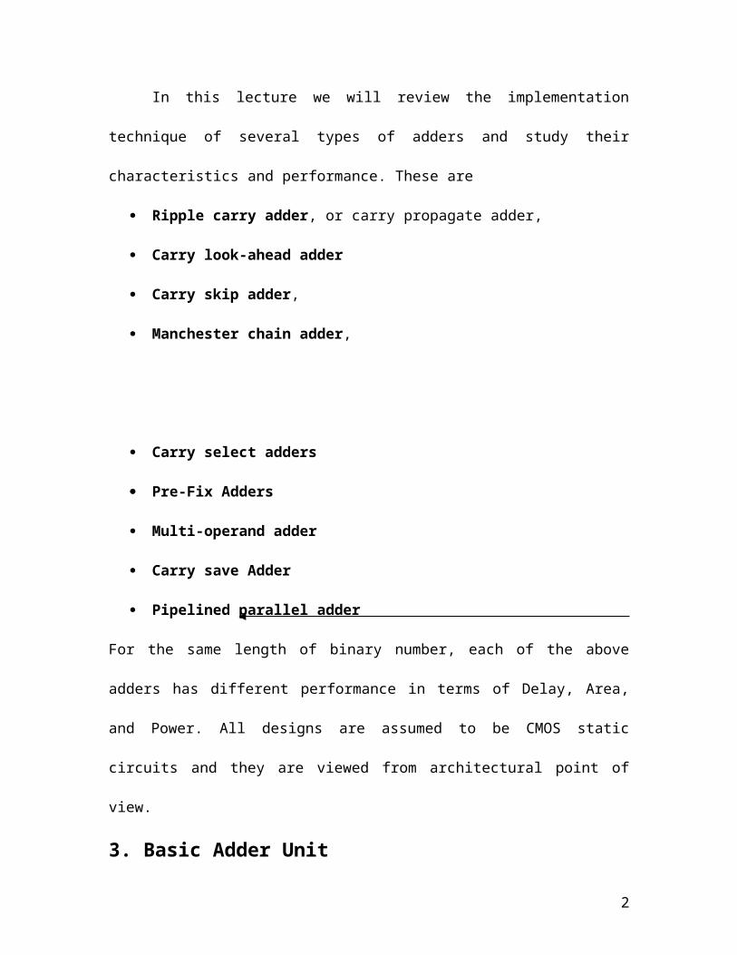
Carry select adders
Pre-Fix Adders
Multi-operand adder
Carry save Adder
Pipelined parallel adder
For the same length of binary number, each of the above adders has different
performance in terms of Delay, Area, and Power. All designs are assumed to be CMOS
static circuits and they are viewed from architectural point of view.
3. Basic Adder UnitThe most basic arithmetic operation is the addition of two binary digits, i.e. bits.
A combinational circuit that adds two bits, according the scheme outlined below, is called
a half adder. A full adder is one that adds three bits, the third produced from a previous
addition operation. One way of implementing a full adder is to utilizes two half adders in
its implementation. The full adder is the basic unit of addition employed in all the adders
studied here
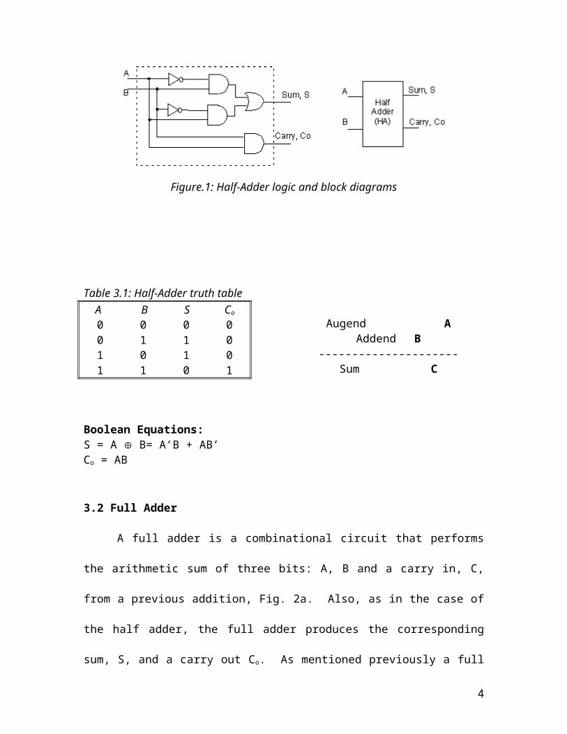
3.1 Half Adder
A half adder is used to add two binary digits together, A and B. It produces S, the
sum of A and B, and the corresponding carry out Co. Although by itself, a half adder is
not extremely useful, it can be used as a building block for larger adding circuits (FA).
One possible implementation is using two AND gates, two inverters, and an OR gate
instead of a XOR gate as shown in Fig. 1.
2

Figure.1: Half-Adder logic and block diagrams
Table 3.1: Half-Adder truth table Augend
AAddend B
---------------------Sum C
Boolean Equations:S = A B= A’B + AB’Co = AB
3.2 Full Adder
A full adder is a combinational circuit that performs the arithmetic sum of three
bits: A, B and a carry in, C, from a previous addition, Fig. 2a. Also, as in the case of the
half adder, the full adder produces the corresponding sum, S, and a carry out Co. As
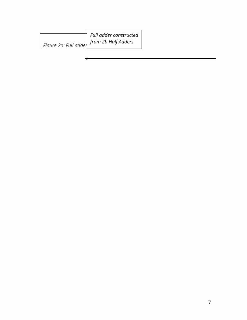
mentioned previously a full adder maybe designed by two half adders in series as shown
below in Figure 2b.
A B S Co
0 0 0 00 1 1 01 0 1 01 1 0 1
3
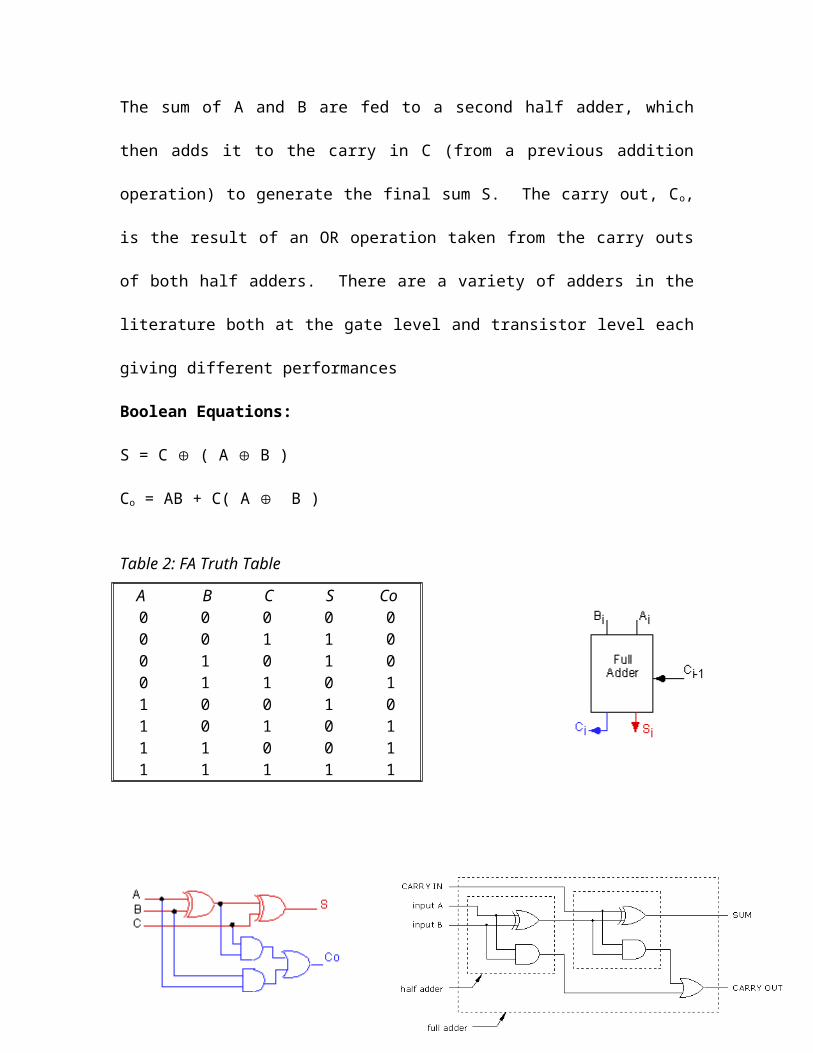
The sum of A and B are fed to a second half adder, which then adds it to the carry in C
(from a previous addition operation) to generate the final sum S. The carry out, C o, is the
result of an OR operation taken from the carry outs of both half adders. There are a
variety of adders in the literature both at the gate level and transistor level each giving
different performances
Boolean Equations:
S = C ( A B )
Co = AB + C( A B )
Table 2: FA Truth Table
A B C S Co0 0 0 0 00 0 1 1 00 1 0 1 00 1 1 0 11 0 0 1 01 0 1 0 11 1 0 0 11 1 1 1 1
4
Figure 2a: Full adder
Full adder constructed from 2b Half Adders
5
4. Parallel AddersParallel adders are digital circuits that compute the addition of variable binary
strings of equivalent or different size in parallel. The schematic diagram of a parallel
adder is shown below in Fig. 3.
Cout
A nbits
nbits S
B nbits
Cin
Fig. 3 Parallel Adder
4.1 Ripple-Carry adderThe ripple carry adder is constructed by cascading full adders (FA) blocks in
series. One full adder is responsible for the addition of two binary digits at any stage of
the ripple carry. The carryout of one stage is fed directly to the carry-in of the next stage.
A number of full adders may be added to the ripple carry adder or ripple carry adders of
different sizes may be cascaded in order to accommodate binary vector strings of larger
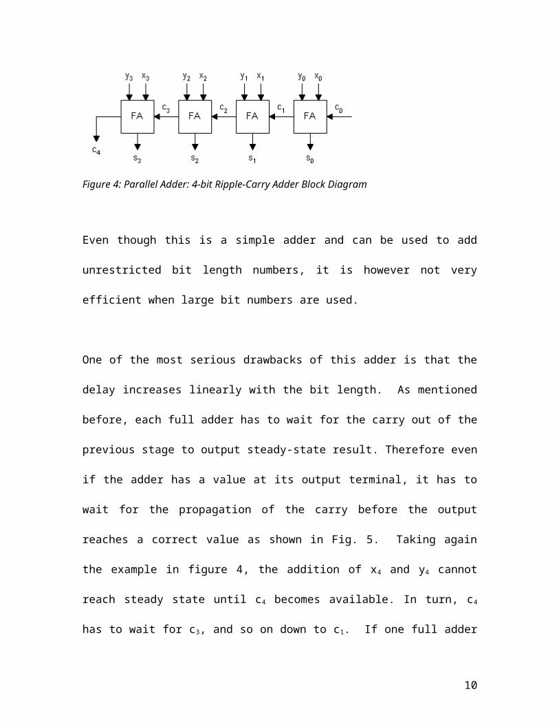
sizes. For an n-bit parallel adder, it requires n computational elements (FA). Figure 4
shows an example of a parallel adder: a 4-bit ripple-carry adder. It is composed of four
full adders. The augend’s bits of x are added to the addend bits of y respectfully of their
binary position. Each bit addition creates a sum and a carry out. The carry out is then
6
transmitted to the carry in of the next higher-order bit. The final result creates a sum of
four bits plus a carry out (c4).
Figure 4: Parallel Adder: 4-bit Ripple-Carry Adder Block Diagram
Even though this is a simple adder and can be used to add unrestricted bit length
numbers, it is however not very efficient when large bit numbers are used.
One of the most serious drawbacks of this adder is that the delay increases linearly with
the bit length. As mentioned before, each full adder has to wait for the carry out of the
previous stage to output steady-state result. Therefore even if the adder has a value at its
output terminal, it has to wait for the propagation of the carry before the output reaches a
correct value as shown in Fig. 5. Taking again the example in figure 4, the addition of x 4
and y4 cannot reach steady state until c4 becomes available. In turn, c4 has to wait for c3,
and so on down to c1. If one full adder takes Tfa seconds to complete its operation, the
final result will reach its steady-state value only after 4.Tfa seconds. Its area is n Afa
A (very) small improvement in area consumption can be achieved if it is known in
advance that the first carry in (c0) will always be zero. (If so, the first full adder can be
replace by a half adder). In general, assuming all gates have the same delay and area of
NAND-2 denoted by Tgate and Agate then this circuit has 3n Tgate delay and 5nAgate. n is
7

the number of full adders. (One must be aware that in Static CMOs, this assumption is
not true). Gate delays depend on intrinsic delay + fanin delay+fanout delay
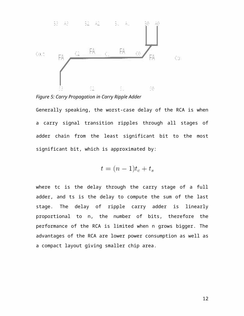
Figure 5: Carry Propagation in Carry Ripple Adder
Generally speaking, the worst-case delay of the RCA is when a carry signal transition
ripples through all stages of adder chain from the least significant bit to the most
significant bit, which is approximated by:
where tc is the delay through the carry stage of a full adder, and ts is the delay to compute
the sum of the last stage. The delay of ripple carry adder is linearly proportional to n, the
number of bits, therefore the performance of the RCA is limited when n grows bigger.
The advantages of the RCA are lower power consumption as well as a compact layout
giving smaller chip area.
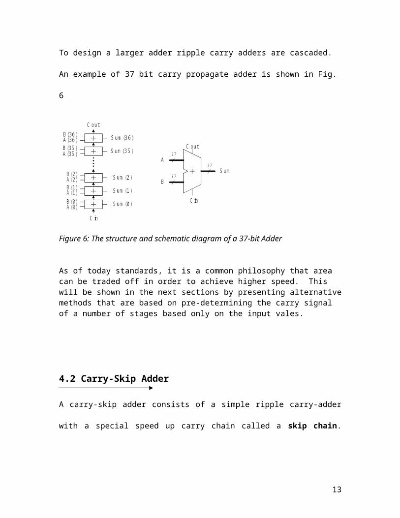
To design a larger adder ripple carry adders are cascaded. An example of 37 bit carry
propagate adder is shown in Fig. 6
8

Figure 6: The structure and schematic diagram of a 37-bit Adder
As of today standards, it is a common philosophy that area can be traded off in order to achieve higher speed. This will be shown in the next sections by presenting alternative methods that are based on pre-determining the carry signal of a number of stages based only on the input vales.
4.2 Carry-Skip Adder
A carry-skip adder consists of a simple ripple carry-adder with a special speed up carry
chain called a skip chain. This chain defines the distribution of ripple carry blocks,
which compose the skip adder.
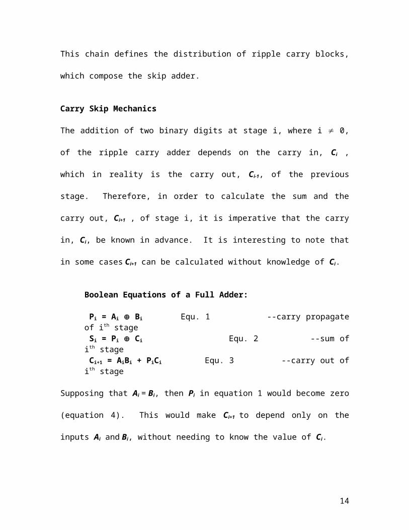
Carry Skip Mechanics
The addition of two binary digits at stage i, where i 0, of the ripple carry adder depends
on the carry in, Ci , which in reality is the carry out, Ci-1, of the previous stage. Therefore,
in order to calculate the sum and the carry out, Ci+1 , of stage i, it is imperative that the
carry in, Ci, be known in advance. It is interesting to note that in some cases Ci+1 can be
calculated without knowledge of Ci.
9
Boolean Equations of a Full Adder:
Pi = Ai Bi Equ. 1 --carry propagate of ith stage Si = Pi Ci Equ. 2 --sum of ith stage Ci+1 = AiBi + PiCi Equ. 3 --carry out of ith stage
Supposing that Ai = Bi, then Pi in equation 1 would become zero (equation 4). This
would make Ci+1 to depend only on the inputs Ai and Bi, without needing to know the
value of Ci.
Ai = Bi Pi = 0 Equ. 4 --from #Equation 1
If Ai = Bi = 0 Ci+1 = AiBi = 0 --from equation 3If Ai = Bi = 1 Ci+1 = AiBi = 1 --from equation 3
Therefore, if Equation 4 is true then the carry out, Ci+1, will be one if Ai = Bi = 1 or zero if
Ai = Bi = 0. Hence we can compute the carry out at any stage of the addition provided
equation 4 holds. These findings would enable us to build an adder whose average time
of computation would be proportional to the longest chains of zeros and of different
digits of A and B.
Alternatively, given two binary strings of numbers, such as the example below, it is very
likely that we may encounter large chains of consecutive bits (block 2) where Ai Bi. In
order to deal with this scenario we must reanalyze equation 3 carefully.
Ai Bi Pi = 1 Equ. 5 --from Equation 1 If Ai Bi Ci+1 = Ci --from Equation 3
In the case of comparing two bits of opposite value, the carry out at that particular stage,
will simply be equivalent to the carry in. Hence we can simply propagate the carry to the
next stage without having to wait for the sum to be calculated.
Two Random Bit Strings:
10

A 10100 01011 10100 01011B 01101 10100 01010 01100 block 3 block 2 block 1 block 0
In order to take advantage of the last property, we can design an adder that is divided into
blocks, as shown in Fig. 7, where a special purpose circuit can compare the two binary
strings inside each block and determine if they are equal or not. In the latter case the
carry entering the block will simply be propagated to the next block and if this is the case
all the carry inputs to the bit positions in that block are all either 0’s or 1’s depending on
the carry in into the block. Should only one pair of bits (Ai and Bi) inside a block be
equal then the carry skip mechanism would be unable to skip the block. In the extreme
case, although still likely, that there exist one such case, where Ai = Bi, in each block,
then no block is skipped but a carry would be generated in each block instead.
Carry Skip Chain
In summary the carry skip chain mechanism (Figure 7) works as follows:
Figure 7: Carry skip chain mechanism
11
Two strings of binary numbers to be added are divided into blocks of equal length. In
each cell within a block both bits are compared for un-equivalence. This is done by
Exclusive ORing each individual cell (parallel operation and already present in the full
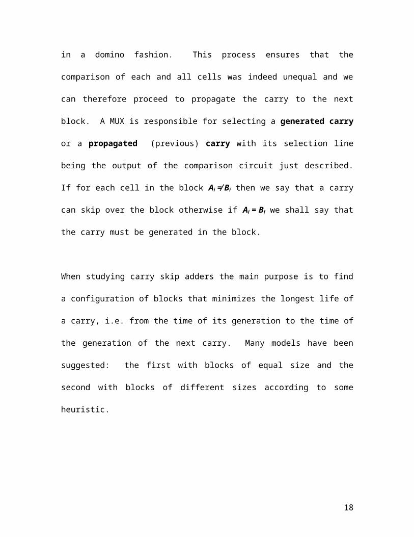
adder) producing a comparison string. Next the comparison string is ANDed within itself
in a domino fashion. This process ensures that the comparison of each and all cells was
indeed unequal and we can therefore proceed to propagate the carry to the next block. A
MUX is responsible for selecting a generated carry or a propagated (previous) carry
with its selection line being the output of the comparison circuit just described. If for
each cell in the block Ai ≠ Bi then we say that a carry can skip over the block otherwise if
Ai = Bi we shall say that the carry must be generated in the block.
When studying carry skip adders the main purpose is to find a configuration of blocks
that minimizes the longest life of a carry, i.e. from the time of its generation to the time of
the generation of the next carry. Many models have been suggested: the first with blocks
of equal size and the second with blocks of different sizes according to some heuristic.
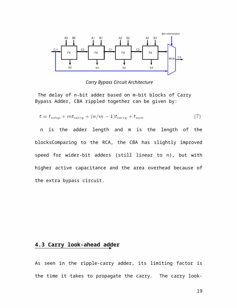
Carry Bypass Circuit Architecture
The delay of n-bit adder based on m-bit blocks of Carry Bypass Adder, CBA rippled together can be given by:
12
n is the adder length and m is the length of the blocksComparing to the RCA, the CBA
has slightly improved speed for wider-bit adders (still linear to n), but with higher active
capacitance and the area overhead because of the extra bypass circuit.
4.3 Carry look-ahead adder
As seen in the ripple-carry adder, its limiting factor is the time it takes to propagate the
carry. The carry look-ahead adder solves this problem by calculating the carry signals in
advance, based on the input signals. The result is a reduced carry propagation time.
To be able to understand how the carry look-ahead adder works, we have to manipulate
the Boolean expression dealing with the full adder. The Propagate P and generate G in a
full-adder, is given as:
Pi = Ai Bi Carry propagateGi = AiBi Carry generate
Notice that both propagate and generate signals depend only on the input bits and thus
will be valid after one gate delay.
The new expressions for the output sum and the carryout are given by:
Si = Pi Ci-1
13
Ci+1= Gi + PiCi
These equations show that a carry signal will be generated in two cases:
1) if both bits Ai and Bi are 1
2) if either Ai or Bi is 1 and the carry-in Ci is 1.
Let's apply these equations for a 4-bit adder:
C1 = G0 + P0C0
C2 = G1 + P1C1 = G1 + P1(G0 + P0C0) = G1 + P1G0 + P1P0C0
C3 = G2 + P2C2 = G2 + P2G1 + P2P1G0 + P2P1P0C0
C4 = G3 + P3C3 = G3 + P3G2 + P3P2G1 + P3P2P1G0 + P3P2P1P0C0
These expressions show that C2, C3 and C4 do not depend on its previous carry-in.
Therefore C4 does not need to wait for C3 to propagate. As soon as C0 is computed, C4
can reach steady state. The same is also true for C2 and C3
The general expression is
Ci+1= Gi + PiGi-1 + PiPi-1Gi-2 + ……. PiPi-1….P2P1G0 + PiPi-1 ….P1P0C0.
This is a two level Circuit. In CMOS however the delay of the function is nonlinerly
dependent on its fan in. Therefore large fanin gates are not practical.
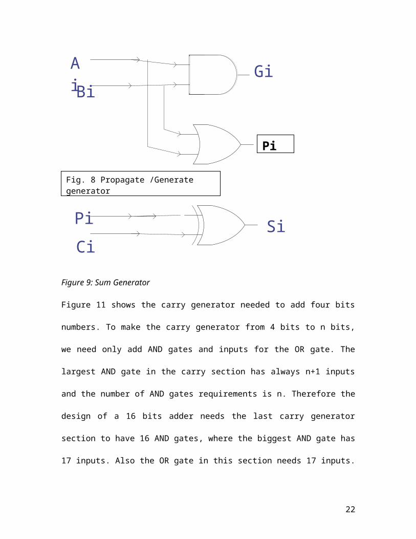
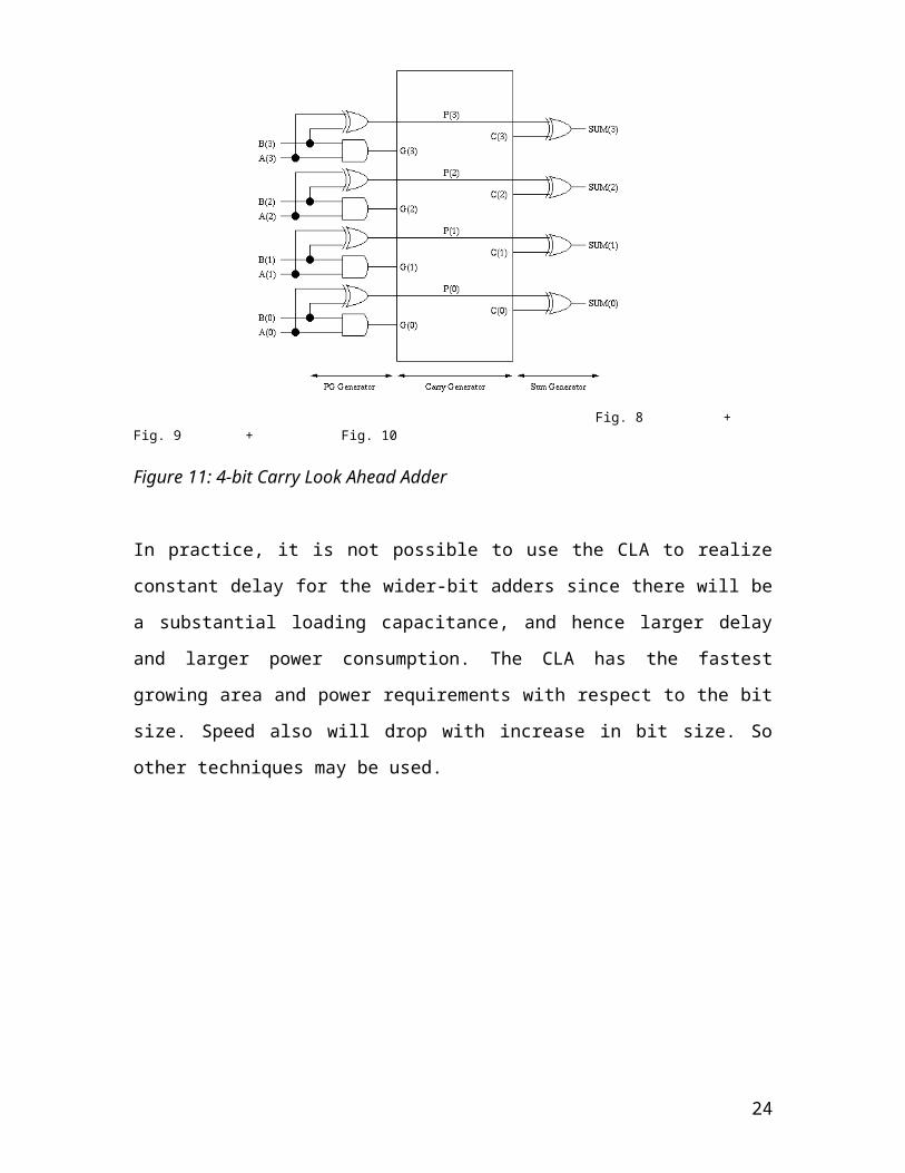
Carry look-ahead adder’s structure can be divided into three parts: the
propagate/generate generator Fig.8, the sum generator Fig. 9 and the carry generator Fig.
10.
14
Figure 9: Sum Generator
Figure 11 shows the carry generator needed to add four bits numbers. To make the carry
generator from 4 bits to n bits, we need only add AND gates and inputs for the OR gate.
The largest AND gate in the carry section has always n+1 inputs and the number of AND
gates requirements is n. Therefore the design of a 16 bits adder needs the last carry
generator section to have 16 AND gates, where the biggest AND gate has 17 inputs. Also
the OR gate in this section needs 17 inputs.
Pi
Fig. 8 Propagate /Generate generator
Ai Bi
Gi
Pi Ci
Si
15

Fig. 10 Look-Ahead Carry generator
The size and fan-in of the gates needed to implement the Carry-Look-ahead adder is usually limited to four, so 4-bit Carry-Look ahead adder is designed as a block. The 4-bit Carry Look Ahead adder block diagram is shown in Fig. 11. The delay of such circuit is 4 levels of logic.
16
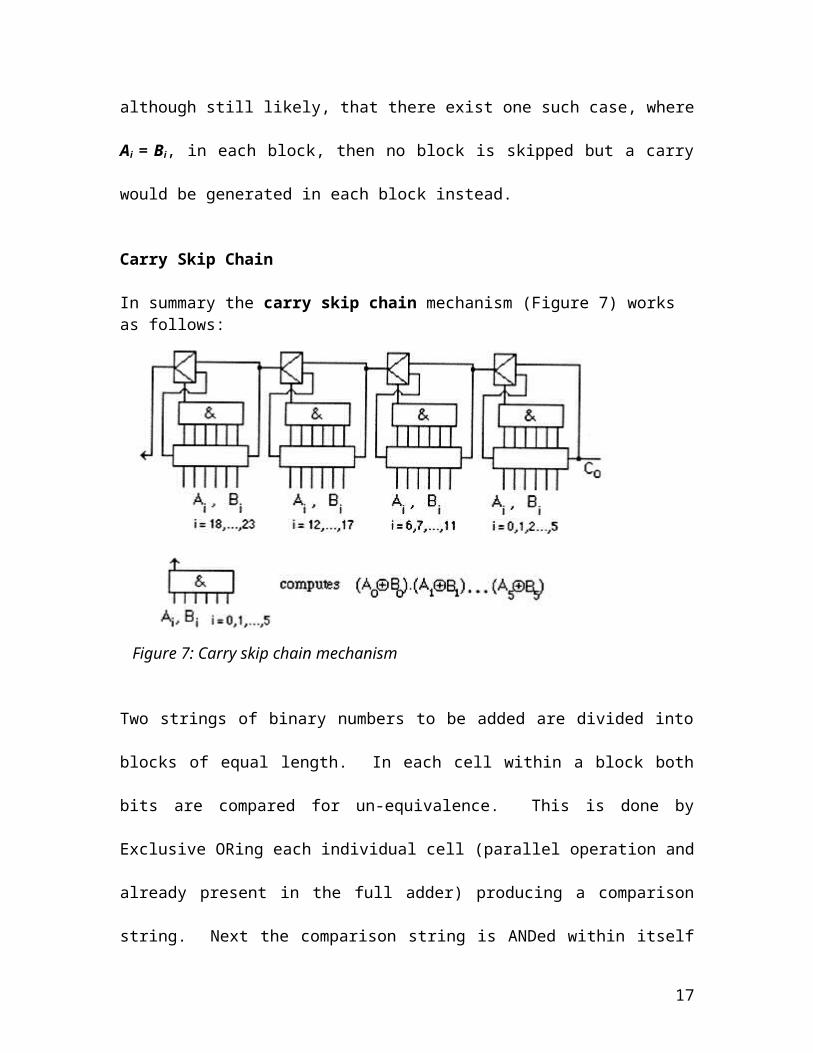
Fig. 8 + Fig. 9 + Fig. 10 Figure 11: 4-bit Carry Look Ahead Adder
In practice, it is not possible to use the CLA to realize constant delay for the wider-bit
adders since there will be a substantial loading capacitance, and hence larger delay and
larger power consumption. The CLA has the fastest growing area and power
requirements with respect to the bit size. Speed also will drop with increase in bit size. So
other techniques may be used.
CLA architecture
17
For example a 32-bit Carry-Look ahead adder can be built by using 8 cascaded 4-bit
Carry-Look ahead adders (Ripple through between the blocks).
Hierarchical Look Ahead Adder
As n increases, the block size has to be limited as well as ripple through delay
accumulates. It is no longer practical to use standard look-ahead method. Instead a two
level carry look-ahead adder is used. In this design, the first level of CLAs generates the
sums as well as second level generate and propagate signals. These signals then are fed to
the 2nd level CLA with carryout of each level to produce the carryout signal. Fig. 26
shows an example of such an adder
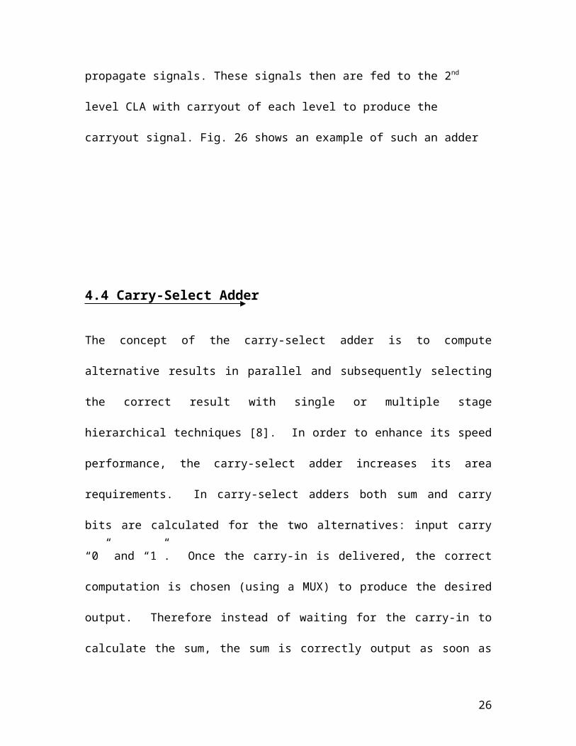
4.4 Carry-Select Adder
The concept of the carry-select adder is to compute alternative results in parallel and
subsequently selecting the correct result with single or multiple stage hierarchical
techniques [8]. In order to enhance its speed performance, the carry-select adder
increases its area requirements. In carry-select adders both sum and carry bits are
calculated for the two alternatives: input carry “0” and “1”. Once the carry-in is
18
delivered, the correct computation is chosen (using a MUX) to produce the desired
output. Therefore instead of waiting for the carry-in to calculate the sum, the sum is
correctly output as soon as the carry-in gets there. The time taken to compute the sum is
then avoided which results in a good improvement in speed. This concept is illustrated in
Fig. 12.
Figure 12: 4-bit carry-select
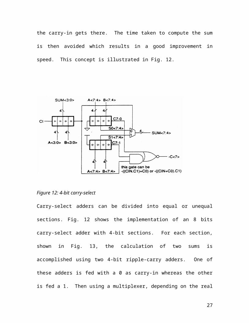
Carry-select adders can be divided into equal or unequal sections. Fig. 12 shows the
implementation of an 8 bits carry-select adder with 4-bit sections. For each section,
shown in Fig. 13, the calculation of two sums is accomplished using two 4-bit ripple-
carry adders. One of these adders is fed with a 0 as carry-in whereas the other is fed a 1.
Then using a multiplexer, depending on the real carryout of the previous section, the
correct sum is chosen. Similarly, the carryout of the section is computed twice and
chosen depending of the carryout of the previous section. The concept can be expanded
19
to any length for example a 16-bits carry-select adder can be composed of four sections
each section is shown in Fig. 13. Each of these sections is composed of two 4-bits ripple-
carry adders. This is referred as linear expansion.
The delay of n-bit carry select adder based on an m-bit CLA blocks can be given by the
following equation when using constant carry number blocks
T=tseup + m tcarry + (n/m) t tmux + t sum
And by the following equation when using successively incremented carry number
blocks respectively.
T=tseup + m tcarry + (2n)1/2 t tmux + t sum
20
Figure 13: One section of a larger Carry Select Adder
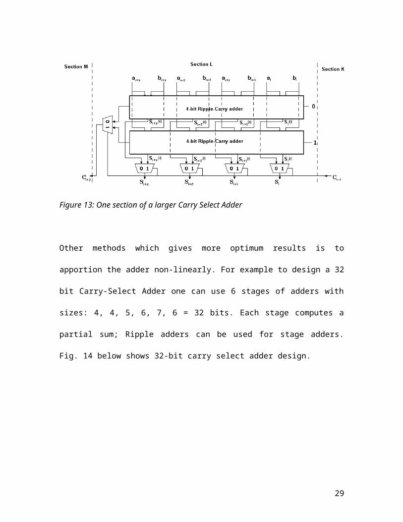
Other methods which gives more optimum results is to apportion the adder non-linearly.
For example to design a 32 bit Carry-Select Adder one can use 6 stages of adders with
sizes: 4, 4, 5, 6, 7, 6 = 32 bits. Each stage computes a partial sum; Ripple adders can be
used for stage adders. Fig. 14 below shows 32-bit carry select adder design.
Figure 14: A 32 bit non-linear Carry Select adder
21
5. Enhancements
In this section we present two kinds of enhancements that can be applied to adders. The
first one is called pipelining and is presented here giving an example. The second
method of enhancement is the use of the Manchester carry chain adder which is based on
the notion that calculates the carryout with as little knowledge of the carry in. The ripple-
carry adder introduced in section 4.1 will be implemented again using these techniques.
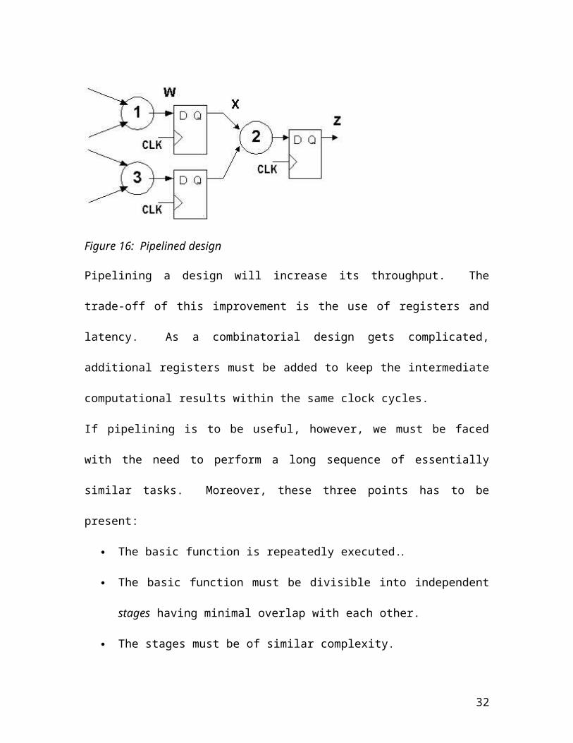
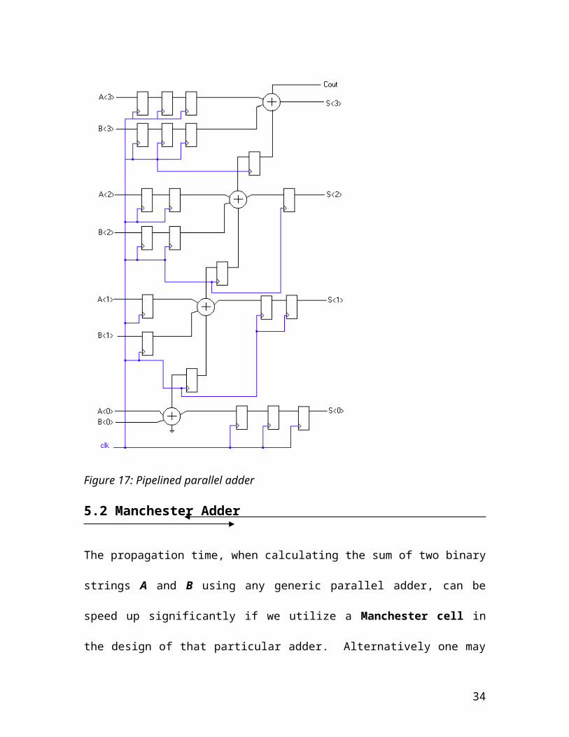
5.1 Pipelined parallel adderPipelining a design means to insert registers into each stage of the design.
Therefore, if a design has K-stages, K registers have to be inserted from an input to an
output. One register will be added for each stage of the circuit.
First, let see how to go from a combinatorial design into a pipelined design. Figure 15
shows a combinatorial circuit composed of three nodes. By inserting a register for each
stage from an input to an output, the pipelined design of Figure 16 is obtained.
22
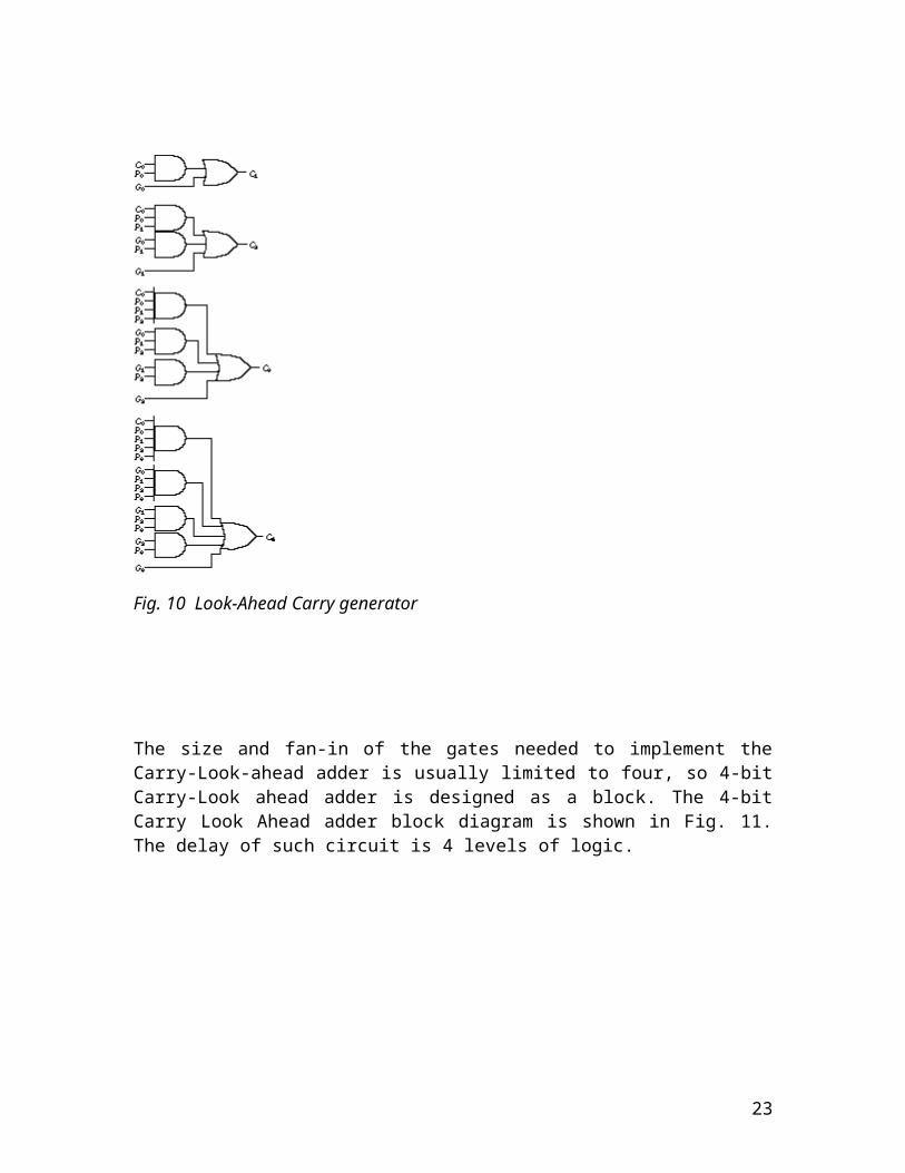
Figure 15: Combinatorial design
Figure 16: Pipelined design
Pipelining a design will increase its throughput. The trade-off of this improvement is the
use of registers and latency. As a combinatorial design gets complicated, additional
registers must be added to keep the intermediate computational results within the same
clock cycles.
If pipelining is to be useful, however, we must be faced with the need to perform a long
sequence of essentially similar tasks. Moreover, these three points has to be present:
The basic function is repeatedly executed..
The basic function must be divisible into independent stages having minimal
overlap with each other.
23
The stages must be of similar complexity.
Parallel adders respect these notions. Therefore let's convert a parallel adder into a
pipelined parallel adder. Recall the 4-bit parallel adder. Figure 17 shows its 4-bit
pipelined parallel adder counterpart.
This adder works as follows: At each clock cycle a new input is applied to the circuit.
Therefore, because of the registers, it takes three clock cycles to get the first result. The
waiting between the first input and the first output is called the latency of the circuit.
This circuit has a latency of three clock cycles. Then, after each clock cycle, a new result
is obtained at the output. This is called the throughput. The throughput of this circuit is
one clock cycle plus Tco (the time from one clock cycle to the output of a register).
The added complexity of such a pipelined adder pays off if long sequences of numbers
are being added.
24
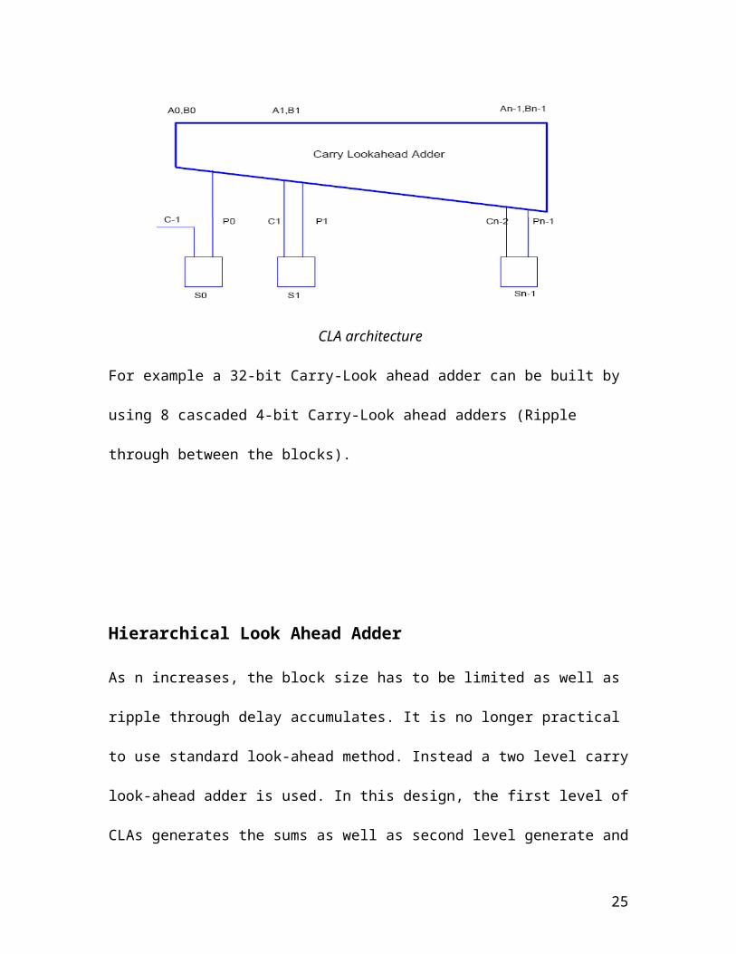
Figure 17: Pipelined parallel adder
5.2 Manchester Adder
The propagation time, when calculating the sum of two binary strings A and B using any
generic parallel adder, can be speed up significantly if we utilize a Manchester cell in the
design of that particular adder. Alternatively one may choose to perform the addition
using any of the two flavours of Manchester adders described later in this section.
25
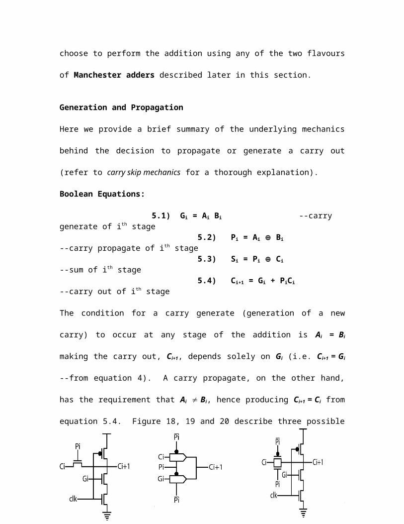
Generation and Propagation
Here we provide a brief summary of the underlying mechanics behind the decision to
propagate or generate a carry out (refer to carry skip mechanics for a thorough
explanation).
Boolean Equations:
5.1) Gi = Ai Bi --carry generate of ith stage 5.2) Pi = Ai Bi --carry propagate of ith stage 5.3) Si = Pi Ci --sum of ith stage 5.4) Ci+1 = Gi + PiCi --carry out of ith stage
The condition for a carry generate (generation of a new carry) to occur at any stage of the
addition is Ai = Bi making the carry out, Ci+1, depends solely on Gi (i.e. Ci+1 = Gi --from
equation 4). A carry propagate, on the other hand, has the requirement that Ai Bi,
hence producing Ci+1 = Ci from equation 5.4. Figure 18, 19 and 20 describe three
possible transistor level implementations for a single carry propagate cell as known as a
Manchester cell (all of these versions implement equation 4 listed above with as little
transistors as possible without compromising speed and performance).
Figure 18: Dynamic Stage Figure 19: Static Stage Figure 20: MUX Stage
26
The Adder
A Manchester carry adder consists of cascaded stages of Manchester propagation cells,
shown above. The optimum amount of cascaded stages may be calculated for a
technology by simulation. For a 16 bit adder example a 4-bit adder made up of four static
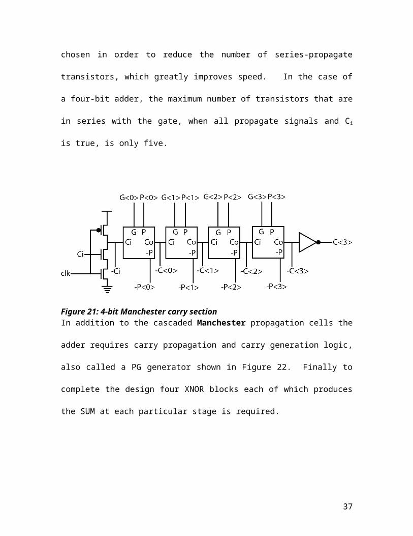
stage cells, shown in figure 21, is chosen in order to reduce the number of series-
propagate transistors, which greatly improves speed. In the case of a four-bit adder, the
maximum number of transistors that are in series with the gate, when all propagate
signals and Ci is true, is only five.
Figure 21: 4-bit Manchester carry sectionIn addition to the cascaded Manchester propagation cells the adder requires carry
propagation and carry generation logic, also called a PG generator shown in Figure 22.
Finally to complete the design four XNOR blocks each of which produces the SUM at
each particular stage is required.
27
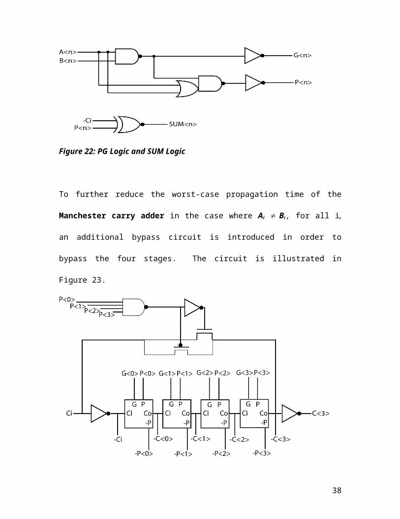
Figure 22: PG Logic and SUM Logic
To further reduce the worst-case propagation time of the Manchester carry adder in the
case where Ai Bi, for all i, an additional bypass circuit is introduced in order to bypass
the four stages. The circuit is illustrated in Figure 23.
Figure 23: Manchester Carry adder with Carry bypass
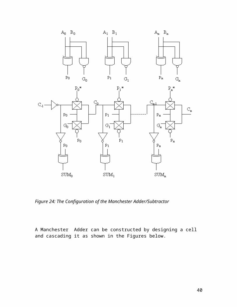
Other Manchester adders’ implementations are possible. One such adder is based on
MUXes called a conflict free Manchester Adder. Although this version reduces even
28
further the propagation time of the adder, it still embodies the core of a Manchester adder
whose ultimate goal is to achieve the reduction of the worst-case time propagation by
employing a Manchester cell.
Figure 24: The Configuration of the Manchester Adder/Subtractor
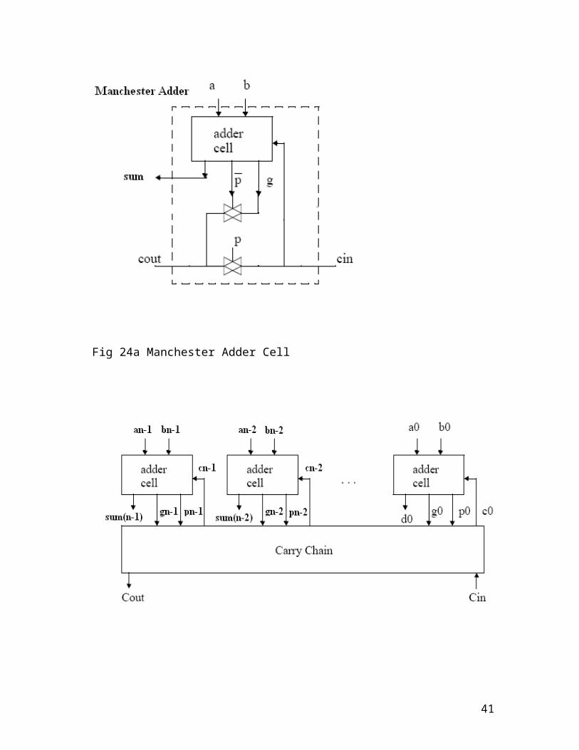
A Manchester Adder can be constructed by designing a cell and cascading it as shown in the Figures below.
29
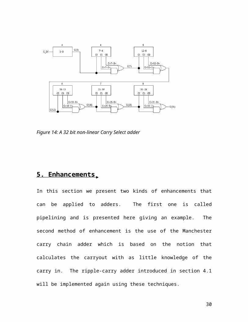
Fig 24a Manchester Adder Cell
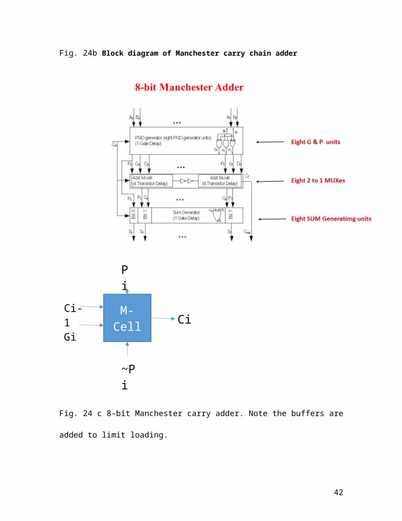
Fig. 24b Block diagram of Manchester carry chain adder
30
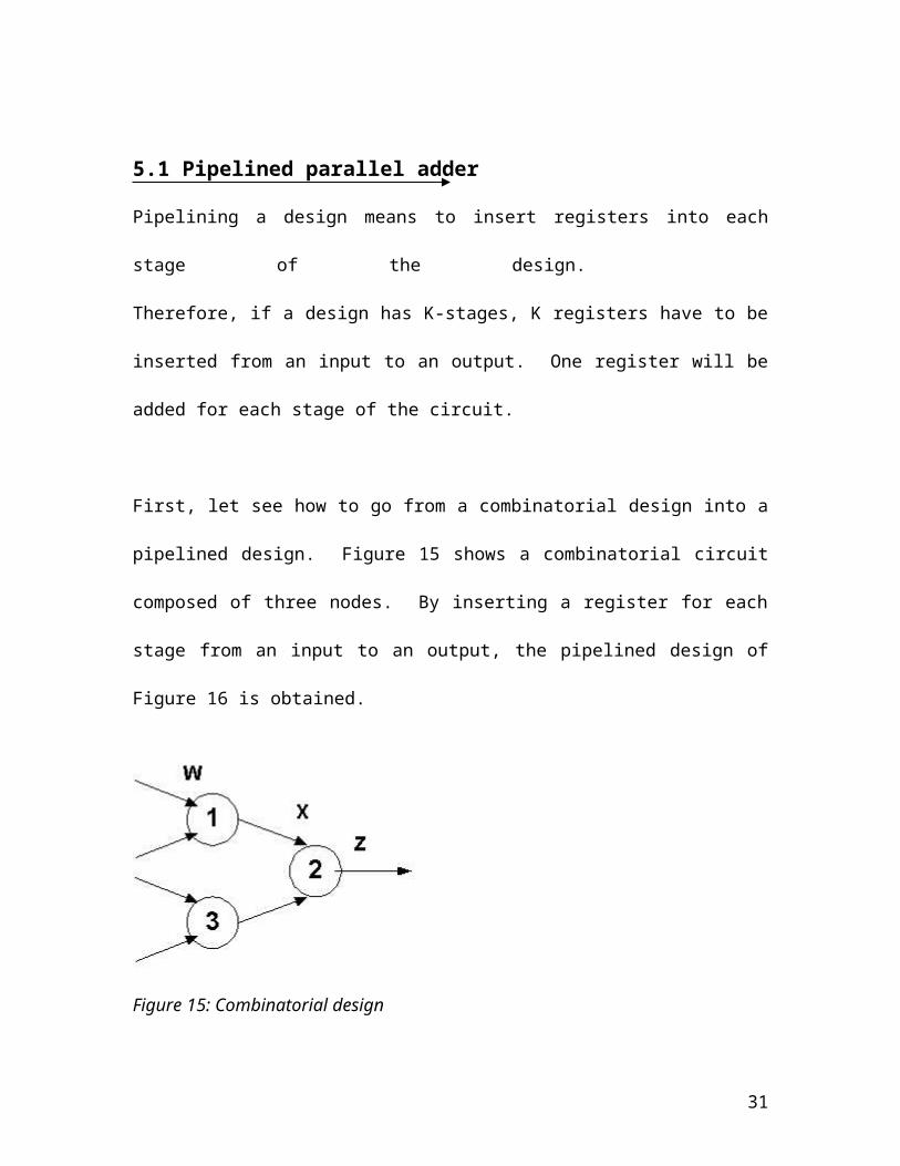
Fig. 24 c 8-bit Manchester carry adder. Note the buffers are added to limit
loading.
31
M-CellCi-1Gi Ci
Pi
~Pi
6. Experiments
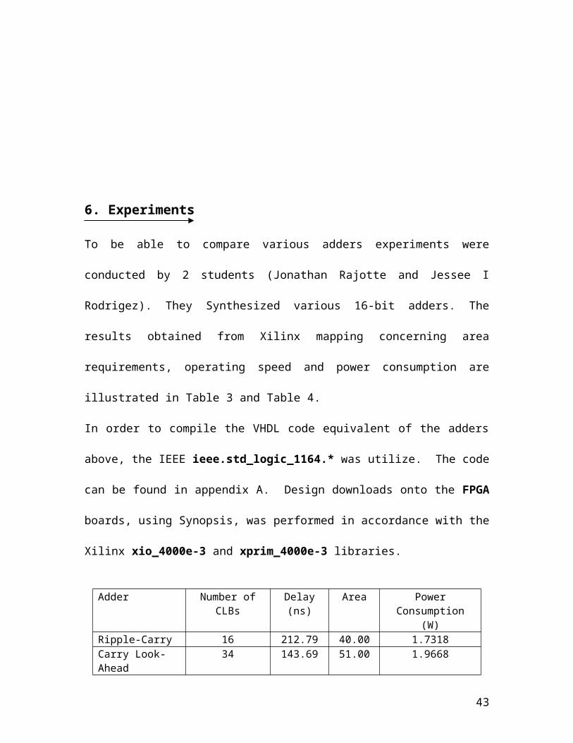
To be able to compare various adders experiments were conducted by 2 students
(Jonathan Rajotte and Jessee I Rodrigez). They Synthesized various 16-bit adders. The
results obtained from Xilinx mapping concerning area requirements, operating speed and
power consumption are illustrated in Table 3 and Table 4.
In order to compile the VHDL code equivalent of the adders above, the IEEE
ieee.std_logic_1164.* was utilize. The code can be found in appendix A. Design
downloads onto the FPGA boards, using Synopsis, was performed in accordance with the
Xilinx xio_4000e-3 and xprim_4000e-3 libraries.
Adder Number of CLBs Delay (ns) Area Power Consumption (W)
Ripple-Carry 16 212.79 40.00 1.7318Carry Look-Ahead 34 143.69 51.00 1.9668Carry-Select 44 102.74 108.00 3.3595
Table 3: Results
From Table.3 we can see that the Carry-Select Adder has the best value for the
parameters: Delay, Power and their AD, ADP. Especially, the delay is 81.86%
less than the Ripple Carry Adder and Carry Look-ahead Adder,
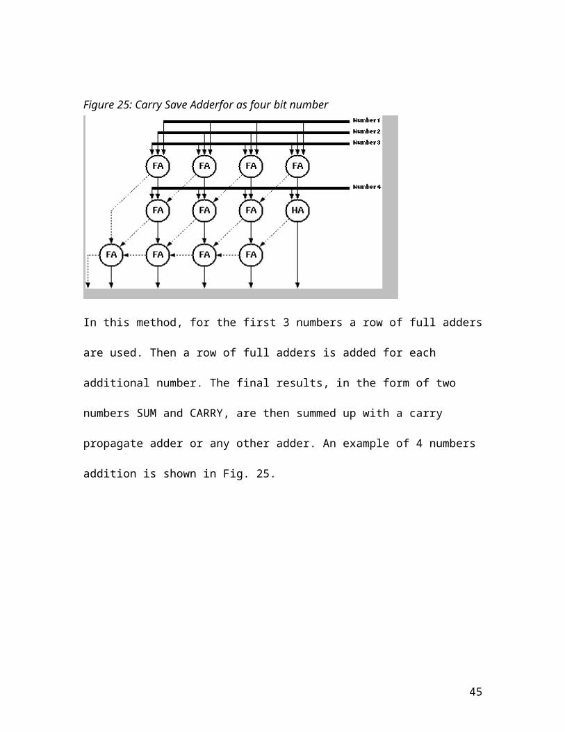
7. Carry Save Adder:
In many cases we need to add several operands together, carry save adders are ideal for
this type of addition
32
A carry save adder consists of a ladder of stand alone full adders, and carries out a
number of partial additions. The principal idea is that the carry has a higher power of 2
and thus is routed to the next column. Doing additions with Carry save adder saves time
and logic.
Figure 25: Carry Save Adderfor as four bit number
In this method, for the first 3 numbers a row of full adders are used. Then a row of full
adders is added for each additional number. The final results, in the form of two numbers
SUM and CARRY, are then summed up with a carry propagate adder or any other adder.
An example of 4 numbers addition is shown in Fig. 25.
33
Large adders design
Large adders require a special design. Most standard adders are modified in a way or
other to be able to use them for larger designs. For example Carry Look Ahead adders are
modified as hierarchical 2 level circuits. This is because as n increases, the block size has
to be limited as well as ripple through delay accumulates. It is no longer practical to use
standard look-ahead method. The hierarchical CLA has two levels. In this design, the first
level of CLAs generates the sums as well as the second level ‘generate and propagate
signals. These signals then are fed to the 2nd level CLA with carryout of each level to
produce the carryout signal. Each Block CLA has a special design. For more details one
can refer to:
“Principles of CMOS VLSI Design” by: N. Weste and K. Eshraghian or
“Fundamentals of Digital Logic with VHDL” by: Brown and Verasenic. (see references).
These references have a section on large adder designs.
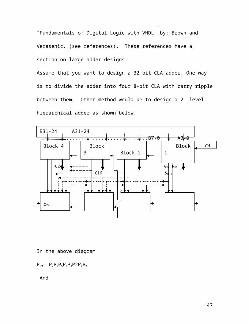
Assume that you want to design a 32 bit CLA adder. One way is to divide the adder into
four 8-bit CLA with carry ripple between them. Other method would be to design a 2-
level hierarchical adder as shown below.
34
In the above diagram
PB0= P7P6P5P4P3P2P1P0
And
GBo= g7 +p7g6 + p7P6G5+ ………………..P7P6P5P4P3P2P1G0
Other carrys then can be obtained using CLA methodology as
c8 = GB0 + PB0 cin
c16 =GB1 + PB1 c8
c24= GB2 + PB2 c16
c32 = GB3 + PB3 c24
Another method is to use a Block CLA, without going into details an example a large 53
bit CLA is shown in Fig 26.
B31-24 A31-24 ………………………............................B7-0 A7-0
Block 4
C24
Block 2 C8
c24
Block 1
GB0 PB0 S0-7
Block 3
C16
35
Cin
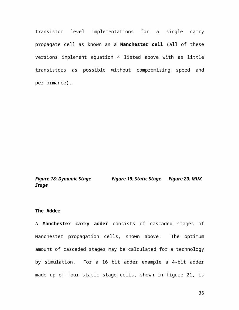
Fig. 26, A 53 bit Carry Look Ahead adder
8. What type of adder is to be used?
Comparing the performance metrics for the 16-bit adders implemented on Xilinx FPGA
board, using Synopsys synthesis tools, the trade offs becomes apparent. As can be seen
there exist an inverse relationship between time delays, operating speed, and circuit area,
in this case the number of CLBs ( measure of the area). The ripple carry adder, the most
basic of flavours, is at the one extreme of this spectrum with the least amount of CLBs
but the highest delay. The carry select adder on the other hand, is at the opposite corner
since it has the lowest delay (half that of the ripple carry’s) but with a larger area required
to compensate for this time gain. Finally, the carry look-ahead is middle ground. Power
dissipation, for this case study, is in direct proportion to the number of CLBs.
For more information on different adders, please see Appendix 3.
36
Carry Propagate/Generate unit
8-Bit BCLA8-Bit BCLA8-Bit BCLA8-Bit BCLA8-Bit BCLA8-Bit BCLA6-Bit BCLA
A53-----------------------------A0 B53-----------------------------B0
P53-----------------------------P0 G53-----------------------------G0
7-Bit BCLA
P53-P48 G53-G48
P47-P40 G47-G40
P39-P32 G39-G32
P31-P24 G31-G24
P23-P16 G23-G16
P15-P8 G15-G8
P7-P0 G7-G0
C53-C48 C47-C40 C39-C32 C31-C24 C23-C16 C15-C8 C7-C0
P0*-G0* P1*-G1* P2*-G2* P3*-G3*P4*G4*
P5*G5*P6*G6*
C7C15C23C31C39C47
C53
54-Bit Summation Unit
P53-----------------------------P0 C53-----------------------------C0
Appendix 3 Some Comparisons of 64 bit adders
For this comparison Synopsys tools were used to perform logic synthesis.
The implemented VHDL codes for all the 64-bit adders are translated into net list files.
The virtex2 series library, XC2V250-4_avg, is used in those 64-bit adders synthesis and targeting because the area and the propagation delay are suitable for these adders.
After synthesizing, the related power consumption, area, and propagation delay are reported.
Synthesis result parameter comparison listings:
Primitive ComponentDelay (ns) Area Power (W) AT PD
4-bit carry ripple adder 72.1 160 0.875 11536 831745 63.058 8-bit carry ripple adder 72.1 160 0.875 11536 831745 63.058 16-bit carry ripple adder 72.1 160 0.875 11536 831745 63.058
4-bit carry look-ahead adder 93.54 288 1.049 26939 2519922 98.123
8-bit carry look-ahead adder 118.9 302 1.163 35908 4269437 138.25
16-bit carry look-ahead adder 124.3 310 1.176 38533 4789651 146.14
two-level 8-bit carry look-ahead adder 31.57 434 1.348 13701 432552 42.56
4-bit carry select adder 24.72 422.5 1.635 10444 258180 40.42 8-bit carry select adder 20.48 394.5 1.575 8079 165465 32.27 16-bit carry select adder 26 356.5 1.479 9269 240994 38.459 Nonlinear Carry select
adder 17.94 412 1.626 7391 132599 29.183 4-bit Manchester adder 27.58 256 1.086 7060 194728 29.9438-bit Manchester adder 27.58 256 1.086 7060 194728 29.943
16-bit Manchester adder 27.58 256 1.086 7060 194728 29.94316-bit Ladner-Fischer
prefix adder 24.79 326 1.23 8081 200341 30.49116-bit Brent-Kung prefix
adder 26.94 290 1.15 7812 210471 30.98116-bit Han-Carlson prefix
adder 25.43 326 1.276 8290 210819 32.44316-bit Kogge-Stone prefix
adder 25.59 428 1.555 10952 280274 39.7864-bit Kogge-Stone adder 11.97 611 1.919 7313 87544 22.97
By, Chen,Kungching—M. Eng. Project_ 2005
37
References
[1] Stefan Sjoholm and Lennart Lind, VHDL for designers, Prentice Hall, 1997
[2] Vitit Kantabutra, “Designing optimum One-Level Carry-Skip Adders” IEEE Transactions on Computers, Vol.42, No.6, June 1993
[3] Luigi Dadda and Vincenzo Piuri, “Pipelined adders” IEEE Transactions on Computers, Vol.45, No.3, March 1996
[4] M. Morris Mano, Digital Design second edition, Prentice Hall, 1991
[5] Carver Mead and Lynn Conway, Introduction to VLSI design, Addison-Wesley Company, 1980
[6] Jien-Chung Lo, “A fast binary adder with conditional carry generation” IEEE Transactions on Computers, Vol.46, No.2, February 1997
[7] N.H.E. Weste and K. Eshraghian, Principle of CMOS VLSI Design, Addison-Wesley Company, 1992
[8] Peter Pirsch, Architectures for digital signal processing, John Wiley & Sons, 1998
[9] A. Guyot, B. Hochet and J.M. Muller, “A way to build efficient Carry-Skip adders”, IEEE Transactions on Computers, pp.1144-1152, October 1987
[10] S. Brown, Z. Verasenic, “Fundamentals of Digital Logic with VHDL,” Mc. Graw Hill, 2nd edition, 2004.
38

Appendix A: VHDL Code of various adders
A.1 Ripple-Carry Adder
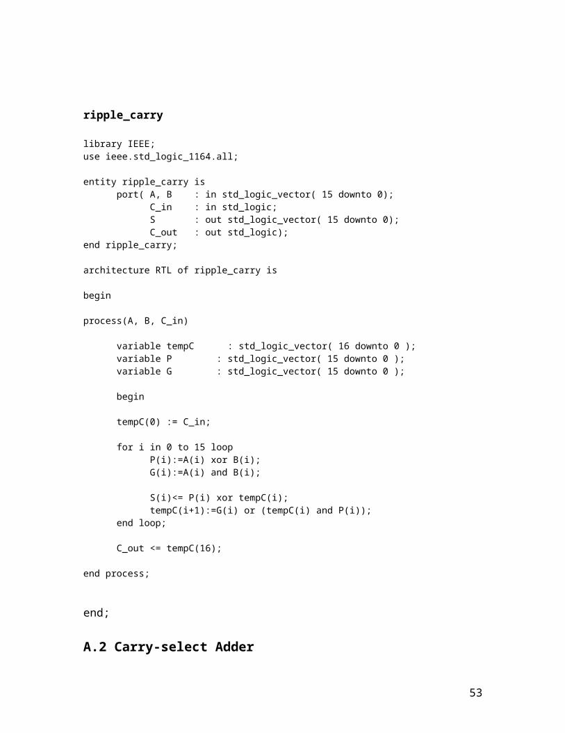
The ripple carry adder is made of only one entity called ripple_carry.
ripple_carry
library IEEE;use ieee.std_logic_1164.all;
entity ripple_carry is port( A, B : in std_logic_vector( 15 downto 0); C_in : in std_logic; S : out std_logic_vector( 15 downto 0); C_out : out std_logic);
end ripple_carry;
architecture RTL of ripple_carry is
begin
process(A, B, C_in)
variable tempC : std_logic_vector( 16 downto 0 );variable P : std_logic_vector( 15 downto 0 );variable G : std_logic_vector( 15 downto 0 );
begin
tempC(0) := C_in;
for i in 0 to 15 loopP(i):=A(i) xor B(i);G(i):=A(i) and B(i);
S(i)<= P(i) xor tempC(i);tempC(i+1):=G(i) or (tempC(i) and P(i));
end loop;
C_out <= tempC(16);
39
end process;
end;
A.2 Carry-select Adder
The carry-select has been implemented using structural VHDL. It uses 4 components carry_select4 which in turn each of them use two components ripple_carry4.
ripple_carry4
library IEEE;use ieee.std_logic_1164.all;
entity ripple_carry4 is port( e, f : in std_logic_vector( 3 downto 0); carry_in : in std_logic; S : out std_logic_vector( 3 downto 0); carry_out : out std_logic);
end ripple_carry4;
architecture RTL of ripple_carry4 is
begin
process(e, f, carry_in)
variable tempC : std_logic_vector( 4 downto 0 );variable P : std_logic_vector( 3 downto 0 );variable G : std_logic_vector( 3 downto 0 );
begin
tempC(0) := carry_in;
for i in 0 to 3 loopP(i):=e(i) xor f(i);G(i):=e(i) and f(i);
S(i)<= P(i) xor tempC(i);tempC(i+1):=G(i) or (tempC(i) and P(i));
end loop;carry_out <= tempC(4);
end process;end;
40
carry_select4
library IEEE;use ieee.std_logic_1164.all;
entity carry_select4 isport( c, d : in std_logic_vector( 3 downto 0); C_input : in std_logic; Result : out std_logic_vector( 3 downto 0); C_output : out std_logic);
end carry_select4;
architecture RTL of carry_select4 is
component ripple_carry4
port( e, f : in std_logic_vector( 3 downto 0); carry_in : in std_logic; S : out std_logic_vector( 3 downto 0); carry_out : out std_logic);
end component;
For S0: ripple_carry4 Use entity work.ripple_carry4(RTL);For S1: ripple_carry4 Use entity work.ripple_carry4(RTL);
signal SUM0, SUM1 : std_logic_vector( 3 downto 0 );signal carry0, carry1 : std_logic;signal zero, one : std_logic;
begin
zero<='0';one<='1';
S0: ripple_carry4 port map( e=>c, f=>d, carry_in=>zero, S=>SUM0, carry_out=>carry0 );S1: ripple_carry4 port map( e=>c, f=>d, carry_in=>one, S=>SUM1, carry_out=>carry1 );
Result<=SUM0 when C_input='0' else SUM1 when C_input='1' else "ZZZZ"; C_output<= (C_input and carry1) or carry0;
end;
carry_select16
library IEEE;use ieee.std_logic_1164.all;
entity carry_select16 is port( A, B : in std_logic_vector( 15 downto 0);
41
C_in : in std_logic; SUM : out std_logic_vector( 15 downto 0); C_out : out std_logic);end carry_select16;
architecture RTL of carry_select16 is
component carry_select4
port( c, d : in std_logic_vector( 3 downto 0); C_input : in std_logic; Result : out std_logic_vector( 3 downto 0); C_output : out std_logic);
end component;
For S0: carry_select4 Use entity work.carry_select4(RTL);For S1: carry_select4 Use entity work.carry_select4(RTL);For S2: carry_select4 Use entity work.carry_select4(RTL);For S3: carry_select4 Use entity work.carry_select4(RTL);
signal tempc1, tempc2, tempc3 : std_logic;
begin
S0: carry_select4 port map( c=>A ( 3 downto 0 ), d =>B ( 3 downto 0 ), C_input=>C_in, Result=>SUM ( 3 downto 0 ), C_output=>tempc1 );S1: carry_select4 port map( c=>A ( 7 downto 4 ), d =>B ( 7 downto 4 ), C_input=>tempc1, Result=>SUM ( 7 downto 4 ), C_output=>tempc2 );S2: carry_select4 port map( c=>A ( 11 downto 8 ), d =>B ( 11 downto 8 ), C_input=>tempc2, Result=>SUM ( 11 downto 8 ), C_output=>tempc3 );S3: carry_select4 port map( c=>A ( 15 downto 12 ), d =>B ( 15 downto 12 ), C_input=>tempc3, Result=>SUM ( 15 downto 12 ), C_output=>C_out );
end;
42
A.3 Carry Look-Ahead Adder
The carry look-ahead adder has been implemented using structural VHDL. It uses two components: half_adder and carry_generator.
half_adder
library IEEE;use ieee.std_logic_1164.all;
entity half_adder isport( A, B : in std_logic_vector( 16 downto 1 );
P, G : out std_logic_vector( 16 downto 1 ) );end half_adder;
architecture RTL of half_adder is
begin
P <= A xor B;G <= A and B;
end;
carry_generator
library IEEE;use ieee.std_logic_1164.all;
entity carry_generator isport( P , G : in std_logic_vector(16 downto 1);
C1 : in std_logic;C : out std_logic_vector(17 downto 1));
end carry_generator;
architecture RTL of carry_generator isbegin
process(P, G, C1)
variable tempC : std_logic_vector(17 downto 1);
begintempC(1) := C1;for i in 1 to 16 loop
tempC(i+1) := G(i) or (P(i) and tempC(i));end loop;
C <= tempC;end process;
end;
43
Look_Ahead_Adder
library IEEE;use ieee.std_logic_1164.all;
entity Look_Ahead_Adder is
port( A, B : in std_logic_vector( 16 downto 1 ); carry_in : in std_logic; carry_out : out std_logic; S : out std_logic_vector( 16 downto 1 ) );
end Look_Ahead_Adder;
architecture RTL of Look_Ahead_Adder is
component carry_generator
port( P , G : in std_logic_vector(16 downto 1); C1 : in std_logic; C : out std_logic_vector(17 downto 1));end component;
component half_adder
port( A, B : in std_logic_vector( 16 downto 1 ); P, G : out std_logic_vector( 16 downto 1) );
end component;
For CG: carry_generator Use entity work.carry_generator(RTL);For HA: half_adder Use entity work.half_adder(RTL);
signal tempG, tempP : std_logic_vector( 16 downto 1 );signal tempC : std_logic_vector( 17 downto 1 );
begin
HA: half_adder port map( A=>A, B=>B, P =>tempP, G=>tempG );CG: carry_generator port map( P=>tempP, G=>tempG, C1=>carry_in, C=>tempC );S <= tempC( 16 downto 1 ) xor tempP;carry_out <= tempC(17);
end;
44
APPENDIX 2 (prepared by Bin Fan & Zuoying Wu)
1. About CarriesThe production of the bit in the addition can be
decomposed into the following two steps, as illustrated in Figure 1.
Figure 1 Steps in addition
The carry ci represents the influence of bits xj and yj for j<i on si. That is
Consequently, the main objective of all methods for reducing the time of addition for conventional representation is to speed up the process for obtaining all carries.
At position i of the addition, consider the relation between the carry-out (ci+1) and the carry-in (ci). The determination of the particular case depends only on the local variables xi and yi and can be performed in parallel (for all i) by the following switching expressions:Case Propagate: Case Generate: Case Kill: Consequently, the carry-out of position i can be expressed in terms of the carry-in to that position as
(1)From the identity and naming , we get an alternative expression for the carry-out (2)
45
Considering a group of bits, expression (1) and (2) can be generalized by replacing the bit-generate gi, the bit-propagate pi, and the bit-alive ai with the corresponding group variables. That is,
(3)By making i=0 in the expression (3), we obtain That is, to compute cj+1 it is sufficient to compute the pair or the pair
.
Figure 2 Computing (g(f,d),a(f,d))
Moreover, as shown in Figure 2, the computation of the variables for the range of bits (f,d) can use the values of these variables for the sub-ranges (f,e) and (e-1,d), with d<e<f. Specifically, from the definitions we obtain the following switching expressions:
2. Prefix AdderThe prefix adder is a structure that is based on considering the carry computation
as a prefix computation. In general, a prefix combinational network of n inputs x0,x1,x2,…,xn-1 uses the associative (arbitrary) operator • to produce the vector of outputs described by
As indicated above, for the carry computation we have
and the operator (implemented by a cell, shown in Figure 3) has as input two pairs of bits and and as output one pair . It is described by the switching
expressions
where as before, and correspond to generate and to alive signals, respectively.
46
With this cell, a variety of networks are used to produce the carries. They are all based on the fact that carry ci corresponds to the generate signal spanning the bit positions (-1) to i-1. We call this generate signal so that where
. A prefix adder is then an interconnection of the above-mentioned cells to produce
for all i. These carries are then used to obtain the sum bits as .To obtain the carries the cells are connected in a recursive manner to produce the
g signals that span an increasing number of bits. That is, beginning with the variables g and a of each bit, the first level of modules produces g and a for groups of two bits, the second level for groups of four bits, and so on. In general, if the right input spans the bits [right2,right1] and the left input spans the bits [left2,left1] with then the output spans the bits [left2,right1] as illustrated in Figure 3. For instance, for right=[5,2] and left=[8,4], the output spans the bits [8,2].
Figure 3 Composition of spans in computing (g,a) signals
An array of cells for an 8-bit adder is shown in Figure 4. The outputs of the cells are labeled with a pair of integers corresponding to the initial and the final bit that is spanned by the output. Because each level produces a doubling of bits spanned, for n power-of-two, the number of the levels is where the additional level is due to the carry-in c0. In the figure for eight bits there are four levels. Although c0 causes the additional level it does not increase the overall delay because the computation of c8 is in parallel to the calculation of the sum bits. The expression for the delay is
Since each level (except the last) has n/2 cells, the number of cells is
(not including the gates to produce gi and ai nor the XOR gates).Since the cells are simple, their delay and area are small, resulting in an effective
implementation. The main disadvantage of this implementation is the large fan-out of some cells as well as the long interconnection wires. For example, in the 8-bit adder there is a cell with internal fan-out of four, so that in general for an adder of n bits that maximum fan-out is n/2+1 where n/2 is the fan-out of the carry tree and the additional 1goes to XOR gate. The large fan-out and long inter-connections produce an increase in the delay, which can be reduced by including buffers. However, the delay of these buffers
47

might still be significant. In such a case, the large fan-out can be eliminated by two approaches, or a combination of both: 1. Increasing the number of levels2. Increasing the number of cells
Figure 4 8-bit prefix adder (Modules to obtain pi,gi and ai signals not shown.)
2.1 Increasing the Number of LevelsThe fan-out can be reduced by increasing the number of levels, as shown in
Figure 5. This is achieved by reducing the parallelism in the determination of the carries. The resulting number of levels in the limit (carry tree fan-out=2) is where the last 1 corresponds again to the stage with one cell, due to c0. The number of cells is the same as for the basic scheme.
48
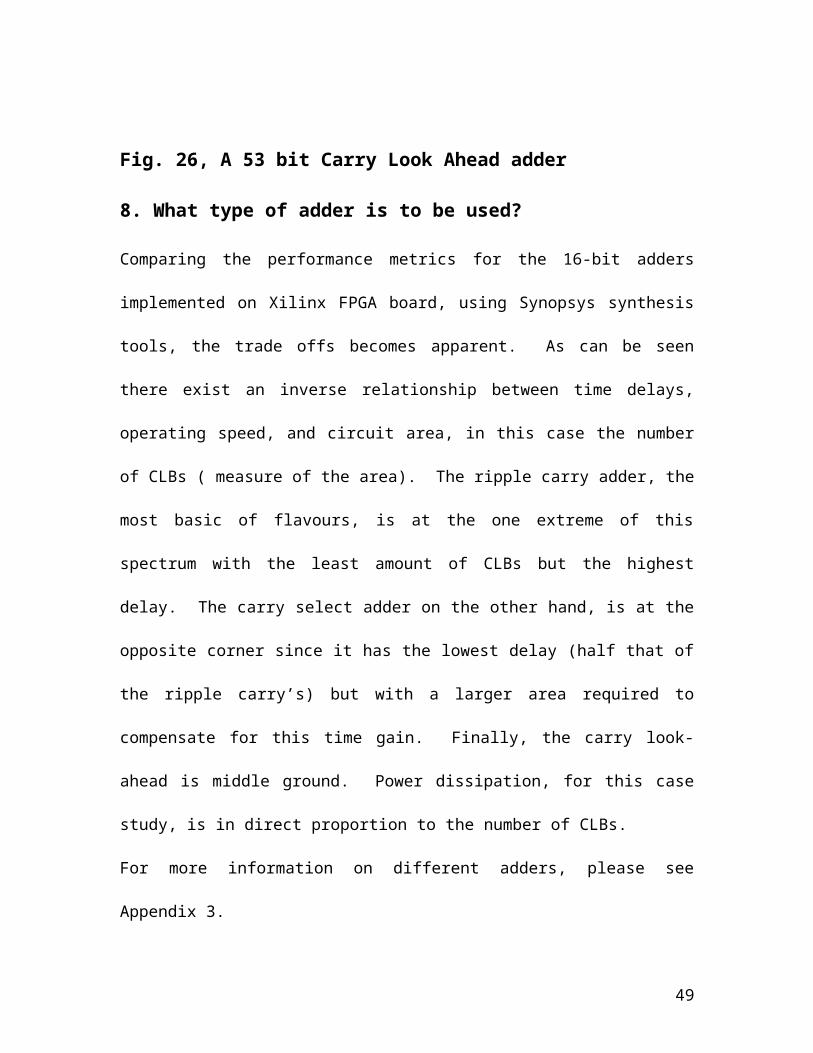
Figure 5 8-bit prefix adder with maximum fan-out of three and five levels
2.2 Increasing the Number of CellsThe maximum fan-out is reduced to two (without increasing the number of levels)
by the structure shown in Figure 6. This structure is constructed as follows:
Level 1 is formed of cells having as inputs neighboring bits. So, groups are formed with bits c0 and 0, with bits 0 and 1, with bits 1 and 2, and so on. Consequently, for n bits there are n cells.
Level 2 combines outputs of cells of level 1 whose indexes differ by 2. That is, c0 and 1, 0 and 2, and so on. There are n-1 cells at this level.
Level 3 combines outputs of cells of level 2 whose indexes differ by 4. That is, c0 and 3, 0 and 4, and so on. There are n-3 cells.
In general, level k combines outputs of level (k-1) whose indexes differ by 2k-1. It has cells.
As in the basic scheme there are levels. As can be seen, the fan-out of all cells is two and the connections are regular. The number of cells is
The number of cells of this scheme is about twice that of the basic scheme. If the number of cells is too high, it is possible to use an intermediate scheme, which has an intermediate maximum fan-out as well as an intermediate number of cells.
49
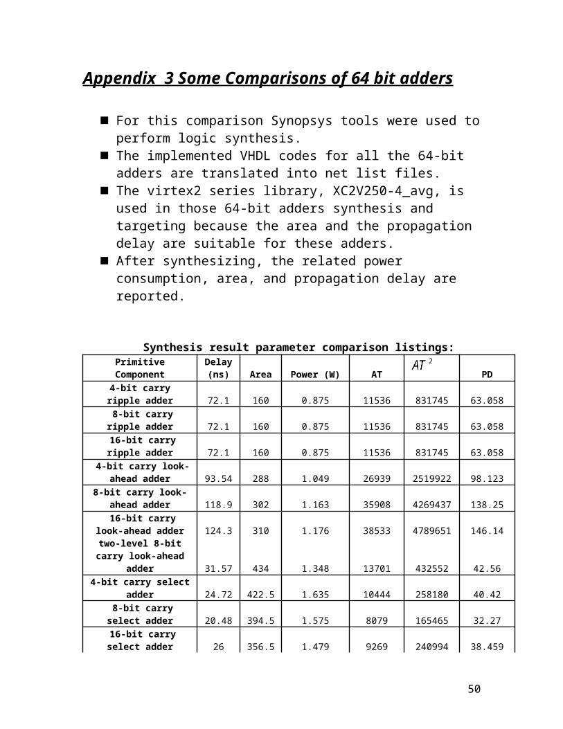
Figure 6 8-bit prefix adder with minimum number of levels and fan-out of two
2.3 Some Parallel Prefix Adder Carry Tree StructuresAs discussed above, the production of the carries in the prefix adder can be
designed in many different ways. Some general graphs are list below.
(1) Ladner-Fischer Parallel Prefix Graph
Figure 7 The Ladner-Fischer parallel prefix graph
Carry stages: ; The number of cells: ; Maximum fan-out: (large fan-out, long wiring)
50
(2) The Kogge-Stone parallel prefix graph
Figure 8 The Kogge-Stone parallel prefix graph
Carry stages: ; The number of cells: ; Maximum fan-out: 2 (extra wiring)
(3) The Brent-Kung parallel prefix graph
Figure 9 The Brent-Kung parallel prefix graph
Carry stages: ; The number of cells: ; Maximum fan-out: 2
51
(4) The Han-Carlson parallel prefix graph
Figure 10 The Han-Carlson parallel prefix graph
Carry stages: ; Maximum fan-out: 2The Han-Carlson structure is a hybrid design combining stages from the Brent-
Kung and Kogge-Stone structures. The middle stages resemble the Kogge-Stone structure and the first and the final stages use the Brent-Kung structure. Comparing to the KS structure, it reduces the wiring and gates but has one more stage.
3. References[1] M.D. Ercegovac and T. Lang, “Digital Arithmetic.” San Francisco: Morgan Daufmann, 2004. ISBN 1-55860-798-6[2] Israel Koren, “Computer Arithmetic Algorithms.” Pub A K Peters, 2002. ISBN 1-56881-160-8
52
Appendix 3 Some Comparisons
Synopsys tools are used to perform logic synthesis. the implemented VHDL codes for all the 64-bit adders are translated
into net list files. The virtex2 series library, XC2V250-4_avg, is used in those 64-bit
adders synthesis and targeting because the area and the propagation delay is suitable for these adders.
After synthesizing, the related power consumption, area, and propagation delay are reported.
From the synthesis, the related FPGA layout schematic is reported.
Synthesis result parameter comparison listings:
Primitive ComponentDelay (ns) Area Power (W) AT PD
4-bit carry ripple adder 72.1 160 0.8745784 11536 831745.6 63.058 8-bit carry ripple adder 72.1 160 0.8745784 11536 831745.6 63.058 16-bit carry ripple adder 72.1 160 0.8745784 11536 831745.6 63.058
4-bit carry look-ahead adder 93.54 288 1.049 26939.52 2519922 98.12346
8-bit carry look-ahead adder 118.9 302 1.1627 35907.8 4269437 138.25
16-bit carry look-ahead adder 124.3 310 1.1757 38533 4789651 146.14
two-level 8-bit carry look-ahead adder 31.57 434 1.348 13701.38 432552 42.56
4-bit carry select adder 24.72 422.5 1.6351 10444.2 258180 40.42 8-bit carry select adder 20.48 394.5 1.5757 8079.36 165465 32.27 16-bit carry select adder 26 356.5 1.4792 9269 240994 38.4592 Nonlinear Carry select
adder 17.94 412 1.6267 7391.28 132599 29.183 4-bit Manchester adder 27.58 256 1.0857 7060.48 194728 29.94368-bit Manchester adder 27.58 256 1.0857 7060.48 194728 29.9436
16-bit Manchester adder 27.58 256 1.0857 7060.48 194728 29.943616-bit Ladner-Fischer
prefix adder 24.79 326 1.23 8081.54 200341 30.491716-bit Brent-Kung prefix
adder 26.94 290 1.15 7812.6 210471 30.98116-bit Han-Carlson prefix
adder 25.43 326 1.2758 8290.18 210819 32.443616-bit Kogge-Stone prefix
adder 25.59 428 1.5546 10952.52 280274 39.7864-bit Kogge-Stone adder 11.97 611 1.919 7313.67 87544 22.97
By, Chen,Kungching—M. Eng. Project_ 2005
53